Embed Size (px)
Citation preview

Bipolar transistors, diodes, ESD protection, filtering and signal conditioning, MOSFETs, and thyristors
Discrete semiconductorsselection guide 2015
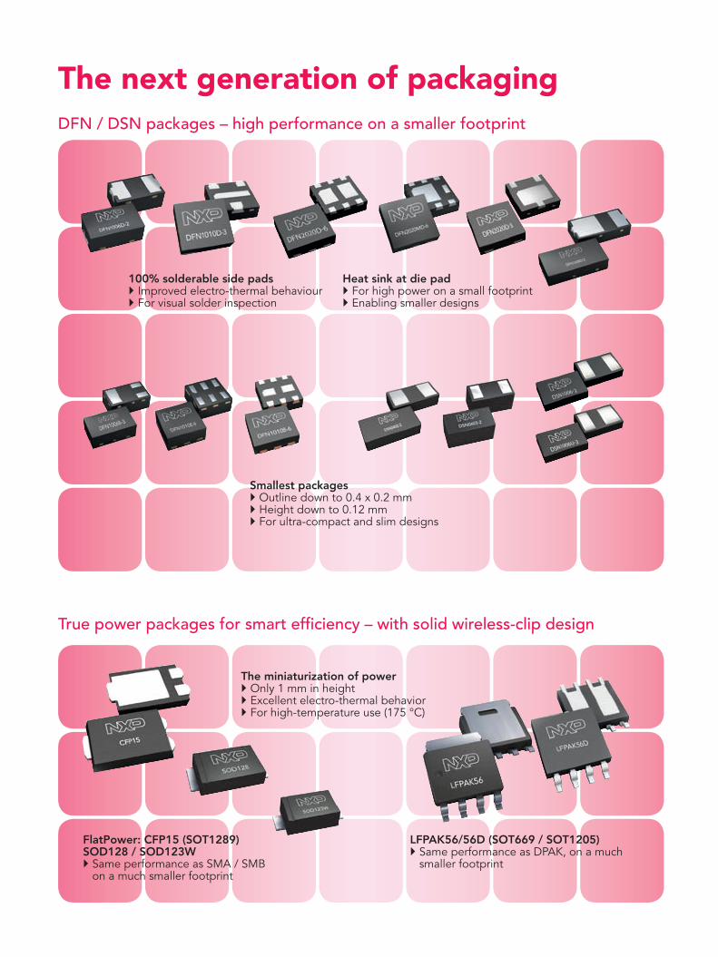
DFN / DSN packages – high performance on a smaller footprint
True power packages for smart efficiency – with solid wireless-clip design
The next generation of packaging
100% solderable side pads Improved electro-thermal behaviour For visual solder inspection
FlatPower: CFP15 (SOT1289)SOD128 / SOD123W Same performance as SMA / SMB
on a much smaller footprint
The miniaturization of power Only 1 mm in height Excellent electro-thermal behavior For high-temperature use (175 °C)
LFPAK56/56D (SOT669 / SOT1205) Same performance as DPAK, on a much
smaller footprint
Heat sink at die pad For high power on a small footprint Enabling smaller designs
Smallest packages Outline down to 0.4 x 0.2 mm Height down to 0.12 mm For ultra-compact and slim designs
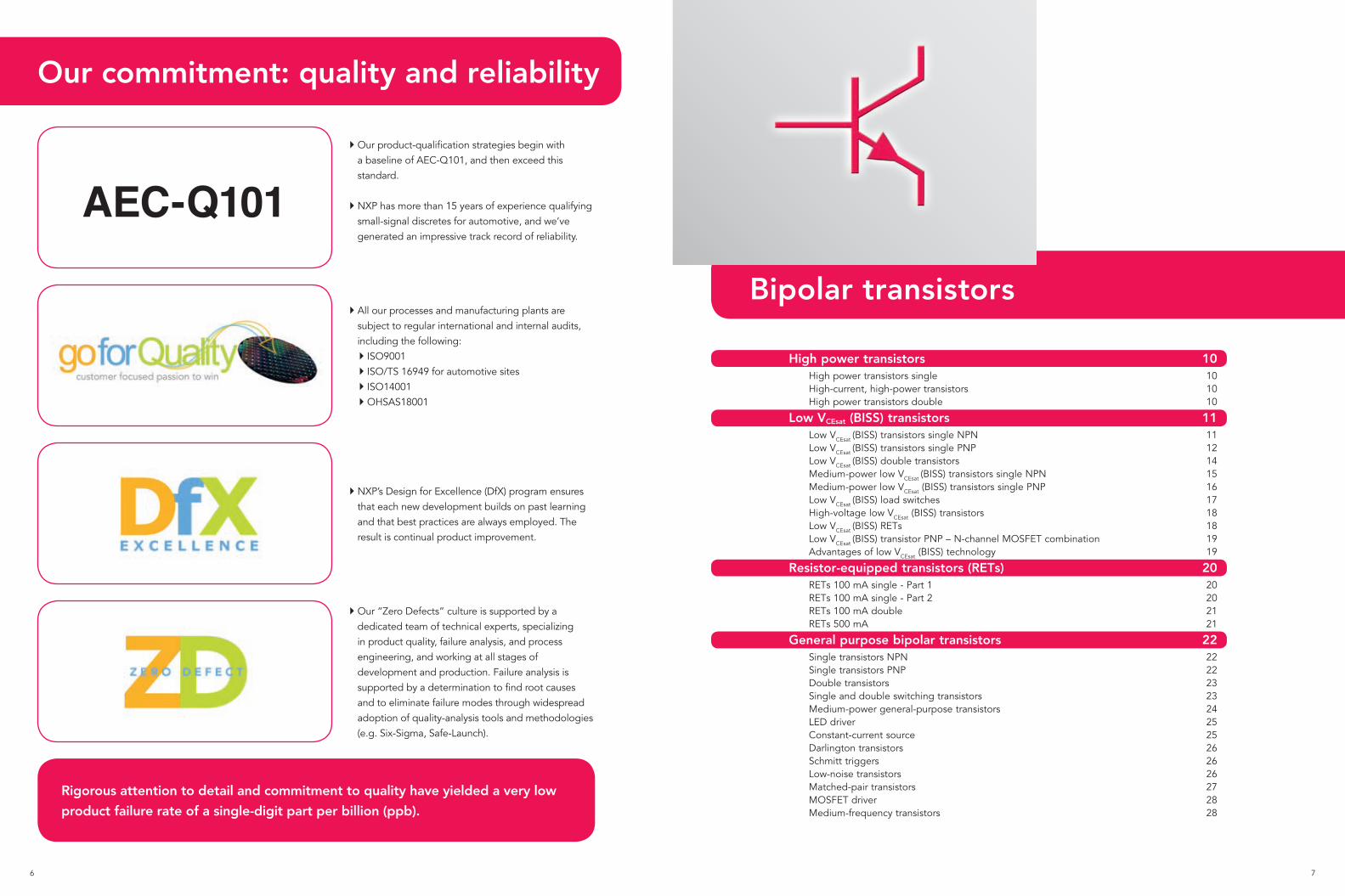
Bipolar transistors
Page 7
ESD protection, filtering and signal
conditioningPage 47
MOSFETsPage 83
ThyristorsPage 141
PackagesPage 147
DiodesPage 29Discretes semiconductors
selection guide 2015
Benefit from interactive features in the online edition of this selection guide: A click on a product type takes you to the corresponding product information page on the NXP website. There you’ll find data sheets and other design-support documents. To access the online selection guide, go to www.nxp.com/discrete_selection_guide
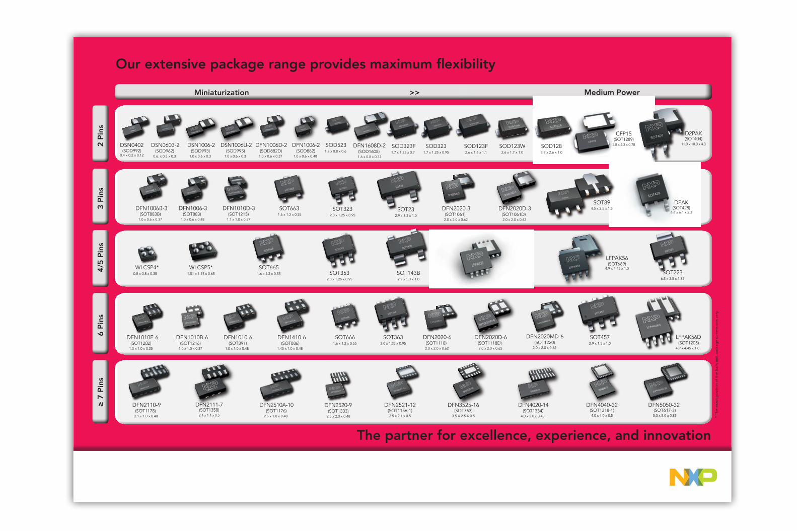
Miniaturization >> Medium Power
SOD5231.2 x 0.8 x 0.6
DFN1006D-2(SOD882D)
1.0 x 0.6 x 0.37
DFN1006-2(SOD882)
1.0 x 0.6 x 0.48
CFP15(SOT1289)
5.8 x 4.3 x 0.78
D2PAK(SOT404)
11.0 x 10.0 x 4.3
DFN2111-7(SOT1358)2.1 x 1.1 x 0.5
LFPAK33(SOT1210)
3.3 x 3.3 x 0.85
DPAK(SOT428)
6.6 x 6.1 x 2.3
DFN1608D-2(SOD1608)1.6 x 0.8 x 0.37
DSN0603-2(SOD962)
0.6. x 0.3 x 0.3
DSN0402(SOD992)
0.4 x 0.2 x 0.12
SOT6631.6 x 1.2 x 0.55
DFN1006-3(SOT883)
1.0 x 0.6 x 0.48
DFN1010D-3(SOT1215)
1.1 x 1.0 x 0.37
DFN1006B-3(SOT883B)
1.0 x 0.6 x 0.37
WLCSP4*0.8 x 0.8 x 0.35
WLCSP5*1.51 x 1.14 x 0.65
SOT6651.6 x 1.2 x 0.55
DFN1410-6(SOT886)
1.45 x 1.0 x 0.48
DFN1010-6(SOT891)
1.0 x 1.0 x 0.48
DFN1010B-6(SOT1216)
1.0 x 1.0 x 0.37
DFN1010E-6(SOT1202)
1.0 x 1.0 x 0.35
SOT6661.6 x 1.2 x 0.55
DFN2020-6(SOT1118)2.0 x 2.0 x 0.62
SOT143B2.9 x 1.3 x 1.0
SOD123W2.6 x 1.7 x 1.0
DFN2020-3(SOT1061)2.0 x 2.0 x 0.62
DFN2020D-3(SOT1061D)2.0 x 2.0 x 0.62
SOT3232.0 x 1.25 x 0.95
SOT3532.0 x 1.25 x 0.95
DFN2020MD-6(SOT1220)
2.0 x 2.0 x 0.62
SOT3632.0 x 1.25 x 0.95
SOD1283.8 x 2.6 x 1.0
SOT894.5 x 2.5 x 1.5
SOT2236.5 x 3.5 x 1.65
SOT232.9 x 1.3 x 1.0
SOT4572.9 x 1.5 x 1.0
DFN2110-9(SOT1178)2.1 x 1.0 x 0.48
DFN2521-12(SOT1156-1)2.5 x 2.1 x 0.5
DFN4040-32(SOT1318-1)4.0 x 4.0 x 0.5
DFN5050-32 (SOT617-3)5.0 x 5.0 x 0.85
DFN2510A-10(SOT1176)
2.5 x 1.0 x 0.48
LFPAK56D (SOT1205)
4.9 x 4.45 x 1.0
DFN2520-9(SOT1333)
2.5 x 2.0 x 0.48
2 Pi
ns3
Pins
4/5
Pins
6 Pi
ns≥
7 Pi
ns
SOD123F2.6 x 1.6 x 1.1
SOD3231.7 x 1.25 x 0.95
SOD323F1.7 x 1.25 x 0.7
LFPAK56(SOT669)
4.9 x 4.45 x 1.0
DFN4020-14(SOT1334)
4.0 x 2.0 x 0.48
DFN3525-16(SOT763)
3.5 X 2.5 X 0.5
DFN2020D-6(SOT1118D)2.0 x 2.0 x 0.62
DSN1006-2(SOD993)
1.0 x 0.6 x 0.3
DSN1006U-2(SOD995)
1.0 x 0.6 x 0.3
Our extensive package range provides maximum flexibility
The partner for excellence, experience, and innovation
* Th
e ex
act
pos
ition
of t
he b
alls
and
pac
kag
e d
imen
sion
s va
ry.
4 5
Bip
ola
r tr
ansi
sto
rs
5
Table of Contents
4
Bipolar transistors 7High power transistors 10
High power transistors single 10High-current, high-power transistors 10High power transistors double 10
Low VCEsat (BISS) transistors 11Low VCEsat (BISS) transistors single NPN 11Low VCEsat (BISS) transistors single PNP 12Low VCEsat (BISS) double transistors 14Medium-power low VCEsat (BISS) transistors single NPN 15Medium-power low VCEsat (BISS) transistors single PNP 16Low VCEsat (BISS) load switches 17High-voltage low VCEsat (BISS) transistors 18Low VCEsat (BISS) RETs 18Low VCEsat (BISS) transistor PNP – N-channel MOSFET combination 19Advantages of low VCEsat (BISS) technology 19
Resistor-equipped transistors (RETs) 20RETs 100 mA single - Part 1 20RETs 100 mA single - Part 2 20RETs 100 mA double 21RETs 500 mA 21
General purpose bipolar transistors 22Single transistors NPN 22Single transistors PNP 22Double transistors 23Single and double switching transistors 23Medium-power general-purpose transistors 24LED driver 25Constant-current source 25Darlington transistors 26Schmitt triggers 26Low-noise transistors 26Matched-pair transistors 27MOSFET driver 28Medium-frequency transistors 28
Diodes 29Schottky barrier diodes and rectifiers 31
Medium-power low VF Schottky rectifiers single ≥1 A - Flatpower packages 31Medium-power low VF Schottky rectifiers single ≥100 mA - DSN packages 32Medium-power low VF Schottky rectifiers single ≥200 mA - leadless (DFN) packages 33Medium-power low VF Schottky rectifiers single ≥200 mA - leaded packages 34Medium-power low VF Schottky rectifiers dual ≥200 mA 35General-purpose Schottky diodes ≤250 mA 36Low-capacitance Schottky diodes 37
Zener diodes 38General-purpose Zener diodes 38Zener diodes specifications 39
Switching diodes 40General-purpose, high-speed switching diodes < 90 V 40General-purpose, high-speed switching diodes 100 V 40General-purpose, switching diodes ≥100 V 41PN-rectifier 41Controlled-avalanche switching diodes 42Low-leakage current-switching diodes 42
Power diodes 43Hyperfast power diodes 43Power Schottky diodes 43Casco diodes 43Ultrafast power diodes 44
ESD protection, filtering and signal conditioning 47Ultra low-capacitance ESD protection devices 53Low-capacitance ESD protection devices 57Standard ESD protection devices 61Application-specific ESD and ESD/EMI solutions 63
USB 2.0 protection and filtering 63Common Mode Filter for USB 2.0 63
USB 3.x and eSATA protection and filtering 64Common Mode Filter for USB 3.x 65Common Mode Filter for video interfaces 66Ethernet protection 66HDMI and memory-card signal conditioning 67Video interface protection 68NFC antenna protection 69LCD and camera protection and filtering 70Audio interface protection and filtering 71Memory- and SIM-card protection and filtering 71Battery and charger protection 71Automotive high-speed network protection 72Automotive in-vehicle network bus line protection 72
Transient voltage suppressor (TVS) diodes 74TVS diodes, 24 / 40 W 74TVS diodes for mobile applications 74TVS diodes, 400 W 75TVS diodes, 600 W 76
MOSFETs 83Small-signal MOSFETs 87
Small-signal MOSFETs in ultra-small DFN1006 and DFN1006B packages 87Small-signal MOSFETs in DFN1010D-3 single and DFN1010B-3 dual package 89Small-signal MOSFETs in DFN2020MD-6 single and DFN2020-6 dual packages 91Small-signal MOSFETs in WLCSP4 and WLCSP6 packages 92 Automotive-compliant small-signal MOSFETs 94Small-signal MOSFETs single (N-channel) 96Small-signal MOSFETs single (P-channel) 98Small-signal MOSFET – Schottky combination 98Small-signal MOSFETs dual 100Small-signal MOSFETs complementary 100
Power MOSFETs 102Power MOSFETs 20 - 25 V 111Power MOSFETs 30 V 112Power MOSFETs 40 V 114Power MOSFETs 55 - 60 V 115Power MOSFETs 75 - 80 V 116Power MOSFETs 100 V 117Power MOSFETs 105 - 150 V 118P channel 118Multi-chip 118Power MOSFETs 200 V 119
Automotive MOSFETs 121Automotive-compliant small-signal MOSFETS 12230 V N-channel automotive TrenchMOS 12840 V N-channel automotive TrenchMOS 12955 - 60 V N-channel automotive TrenchMOS 13175 - 80 V N-channel automotive TrenchMOS 134100 V N-channel automotive TrenchMOS 136TrenchPLUS MOSFETs 138
Thyristors 141AC Thyristor Triacs / AC Thyristors / TOPTriacs 142
AC Thyristors Triacs 142AC Thyristors 142Temperature and Overload Protected Triacs (TOPTriacs) 142
3-quadrant Hi-Com 1434-quadrant triacs 144Silicon Controlled Rectifiers 145
Packages 147Package details and packing methods 148
Package details and packing methods SMD 148Package details and packing methods WLCSP 151Packing details glass diodes, single ended and through hole packages 153
Package cross reference 154Package cross reference list 154Package cross reference matrix 157
Product orientation (tape and reel pack) 160Packing methods 161
Tape and reel pack for SMD and WLCSP packages 159Reel pack axial tape for glass diodes 161Ammo pack axial tape for glass diodes 162Tube pack for through hole packages 163
Minimized outline drawings and reflow soldering footprint 164
6 7
Bipolar transistors
High power transistors 10High power transistors single 10High-current, high-power transistors 10High power transistors double 10
Low VCEsat (BISS) transistors 11Low VCEsat (BISS) transistors single NPN 11Low VCEsat (BISS) transistors single PNP 12Low VCEsat (BISS) double transistors 14Medium-power low VCEsat (BISS) transistors single NPN 15Medium-power low VCEsat (BISS) transistors single PNP 16Low VCEsat (BISS) load switches 17High-voltage low VCEsat (BISS) transistors 18Low VCEsat (BISS) RETs 18Low VCEsat (BISS) transistor PNP – N-channel MOSFET combination 19Advantages of low VCEsat (BISS) technology 19
Resistor-equipped transistors (RETs) 20RETs 100 mA single - Part 1 20RETs 100 mA single - Part 2 20RETs 100 mA double 21RETs 500 mA 21
General purpose bipolar transistors 22Single transistors NPN 22Single transistors PNP 22Double transistors 23Single and double switching transistors 23Medium-power general-purpose transistors 24LED driver 25Constant-current source 25Darlington transistors 26Schmitt triggers 26Low-noise transistors 26Matched-pair transistors 27MOSFET driver 28 Medium-frequency transistors 28
Our product-qualification strategies begin with a baseline of AEC-Q101, and then exceed this standard.
NXP has more than 15 years of experience qualifying small-signal discretes for automotive, and we’ve generated an impressive track record of reliability.
All our processes and manufacturing plants are subject to regular international and internal audits, including the following: ISO9001 ISO/TS 16949 for automotive sites ISO14001 OHSAS18001
NXP’s Design for Excellence (DfX) program ensures that each new development builds on past learning and that best practices are always employed. The result is continual product improvement.
Our “Zero Defects” culture is supported by a dedicated team of technical experts, specializing in product quality, failure analysis, and process engineering, and working at all stages of development and production. Failure analysis is supported by a determination to find root causes and to eliminate failure modes through widespread adoption of quality-analysis tools and methodologies (e.g. Six-Sigma, Safe-Launch).
Our commitment: quality and reliability
Rigorous attention to detail and commitment to quality have yielded a very low
product failure rate of a single-digit part per billion (ppb).
8 9
Bip
ola
r tr
ansi
sto
rs
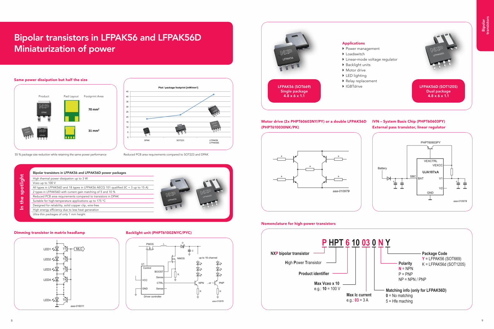
Bipolar transistors in LFPAK56 and LFPAK56D Miniaturization of power
Backlight unit (PHPT61002NYC/PYC)
0
5
10
15
20
25
30
35
40
45
DPAK SOT223 LFPAK56LFPAK56D
Ptot / package footprint [mW/mm ]
Reduced PCB area requirements compared to SOT223 and DPAK
Applications Power management Loadswitch Linear-mode voltage regulator Backlight units Motor drive LED lighting Relay replacement IGBTdrive
Same power dissipation but half the size
55 % package size reduction while retaining the same power performance
Product Pad Layout Footprint Area
Bipolar transistors in LFPAK56 and LFPAK56D power packages
High thermal power dissipation up to 3 W
Vceo up to 100 V
All types in LFPAK56D and 18 types in LFPAK56 AECQ 101 qualified (IC = 3 up to 15 A)
2 types in LFPAK56D with current gain matching of 5 and 10 %
Reduced PCB area requirements compared to transistors in DPAK
Suitable for high-temperature applications up to 175 °C
Designed for reliability, solid copper clip, wire-free
High energy efficiency due to less heat generation
Ultra-thin packages of only 1 mm height
In t
he s
po
tlig
ht
LFPAK56 (SOT669)Single package
4.8 x 6 x 1.1
LFPAK56D (SOT1205)Dual package4.8 x 6 x 1.1
Motor drive (2x PHPT60603NY/PY) or a double LFPAK56D
(PHPT610030NK/PK)
Dimming transistor in matrix headlamp
Nomenclature for high-power transistors
P HPT 6 10 03 0 N Y NXP bipolar transistor
High Power Transistor
Product identifier
Max Vceo x 10 e.g.: 10 = 100 V
Max Ic current e.g.: 03 = 3 A
Matching info (only for LFPAK56D) 0 = No matching 5 = Hfe maching
Package Code Y = LFPAK56 (SOT669) K = LFPAK56d (SOT1205) Polarity
N = NPN P = PNP NP = NPN / PNP
IVN – System Basis Chip (PHPT60603PY)
External pass transistor, linear regulator
10 11
Bip
ola
r tr
ansi
sto
rs
High-power transistors (double)
Package
LFPAK56D (SOT1205)
Size (mm) 4.8 x 6 x 1.1
VCEO
(V)IC
(A)ICM (A)
hFE
typ@ IC(A)
@ VCE
(V)RCEsat typ. @ IC/IB=10
VCEsat typ (mV);
IC = 0.5 A;IB = 0.05 A
VCEsat
max (mV)
@ IC(A)
@ IB(A)
PolarityhFE1/
hFE2
100 3 6 150 0.5 10
80 50 300 3 0.2 2XNPN - PHPT610030NK
125 70 400 3 0.2 2XPNP - PHPT610030PK
80 / 125 50 / 70 300 / 400 3 0.2 NPN/PNP - PHPT61003NPK
80 50 300 3 0.2 2XNPN 0.95 PHPT610035NK
125 70 400 3 0.2 2XPNP 0.9 PHPT610035PK
High-power transistors (single)
Package
LFPAK56(SOT669)
Size (mm) 4.8 x 6 x 1.1
VCEO
(V)IC
(A)ICM (A)
hFE
typ@ IC(A)
@ VCE
(V)RCEsat typ. @ IC/IB=10
VCEsat typ (mV);IC = 0.5 A;IB = 0.05 A
VCEsat
max (mV)
@ IC(A)
@ IB(A)
Polarity
60 3
8
200 / 400 0.5 2 60 50 270 3 0.3 NPN PHPT60603NY
200 / 400 0.5 2 80 70 360 3 0.3 PNP PHPT60603PY
100
3150 / 250 0.5 10 75 50 330 3 0.3 NPN PHPT61003NY
150 / 220 0.5 10 110 70 360 2 0.2 PNP PHPT61003PY
2 6150 / 250 0.5 10 80 50 300 2 0.2 NPN PHPT61002NYC
150 / 220 0.5 10 125 70 400 2 0.2 PNP PHPT61002PYC
High-current, high-power transistors
Package
LFPAK56(SOT669)
Size (mm) 4.8 x 6 x 1.1
VCEO (V)
IC (A)
hFE typ
@ IC(A)
@ VCE
(V)Polarity
40 6 200/400 0.5 2 NPN PHPT60406NY
40 6 200/400 0.5 2 PNP PHPT60406PY
40 10 200/400 0.5 2 NPN PHPT60410NY
40 10 200/400 0.5 2 PNP PHPT60410PY
40 15 200/400 0.5 2 NPN PHPT60415NY
40 15 200/400 0.5 2 PNP PHPT60415PY
60 6 200/400 0.5 2 NPN PHPT60606NY
60 6 150/250 0.5 2 PNP PHPT60606PY
60 10 200/400 0.5 2 NPN PHPT60610NY
60 10 150/250 0.5 2 PNP PHPT60610PY
100 6 150/250 0.5 10 NPN PHPT61006NY
100 6 150/220 0.5 10 PNP PHPT61006PY
100 10 150/250 0.5 10 NPN PHPT61010NY
100 10 150/220 0.5 10 PNP PHPT61010PY
High-power transistors Low VCEsat (BISS) transistors
Low VCEsat (BISS) transistors single NPN
Package
SOT23SOT323 (SC-70)
SOT363 (SC-88)
DFN1006-3 (SOT883)
DFN1006B-3 (SOT883B)
DFN1010D-3(SOT1215)
Size (mm) 2.9 x 1.3 x 1.0
2.0 x 1.25 x 0.95
2.0 x 1.25 x 0.95
1.0 x 0.6 x 0.48
1.0 x 0.6 x 0.37
1.1 x 1.0 x 0.37
Ptot (mW) 480 350 430 250 250 750
VCEO
(V)IC
(A)ICM
(A)hFE
min/typ@ IC(A)
@ VCE
(V)
RCEsat typ (mΩ);IC/IB =
10
VCEsat typ (mV);
IC = 0.5 A;
IB = 0.05 A
VCEsat
max (mV)
@ IC(A)
@ IB(A)
15 0.5 1200 / 325 0.01 2 360 - 250 0.5 0.05 PBSS2515M PBSS2515MB
200 / 425 0.01 2 300 200 250 0.5 0.05
20
1 3 350 / 470 0.1 2 220 110 2) 250 1 0.05 PBSS4120T
2 5 220 / 330 0.1 2 80 45 310 3 0.3 PBSS4320T
4.3 8 300 / 550 0.5 2 36 21 220 4 0.2 PBSS4021NT
30
11.5 230 / 380 0.5 2 175 90 235 1 0.1 PBSS4130QA
3 300 / 450 0.5 2 240 120 2) 270 1 0.05 PBSS4130T
2 3300 / 450 0.5 2 120 70 320 2 0.2 PBSS4230T
230 / 380 0.5 2 135 75 350 2 0.2 PBSS4230QA
2.6 5 300 / 500 0.5 2 76 80 320 3 0.3 PBSS4032NT 3)
40
0.5 1200 / 550 0.01 2 380 200 2) 250 0.5 0.05 PBSS2540M PBSS2540MB
200 / 350 0.01 2 380 190 250 0.5 0.05
2.0
300 / 440 0.5 5 240 130 500 1 0.1 PBSS4140U
300 / 510 0.5 5 230 120 500 1 0.1 PMMT491A
300 / 420 0.5 5 150 130 500 1 0.1 PBSS4140T
3.0
300 / - 0.5 5 280 140 510 2 0.2
350 / 470 0.1 2 120 70 320 2 0.2 PBSS4240Y
300 / 450 0.5 2 120 70 320 2 0.2 PBSS4240T
50 2 5 300 / 495 0.5 2 100 60 260 2 0.2 PBSS4350T
60
1.0
1.5 150 / 240 0.5 2 170 90 235 1 0.1 PBSS4160QA
200 / 420 0.5 5 230 120 280 1 0.1 PBSS4160U
200 / 350 0.5 5 200 110 250 1 0.1 PBSS4160T
2 3 150 / 240 0.5 2 125 75 350 2 0.2 PBSS4260QA
3.8 8 300 / 500 0.5 2 46 29 200 3 0.3 PBSS4041NT
100 1.0 3.0150 / 400 0.25 10 160 80 200 1 0.1 PBSS8110Y
150 / 300 0.25 10 165 70 200 1 0.1 PBSS8110T
1) IC / IB = 20 2) VCEsat (max) 3) Optimized for high-speed switching
M3D088
types in bold represent new products
New low VCEsat transistors up to 2 A in DFN1010D-3: 2 A on 1.1 mm2 footprint
High IC performance on ultra-small footprint
VCE 30 and 60 V
Leadless DFN1010D-3 (SOT1215) SMD package with solderable sidepads (1.1 x 1.0 x 0.37)
AEC-Q101 qualifiedIn t
he s
po
tlig
ht
12 13
Bip
ola
r tr
ansi
sto
rs
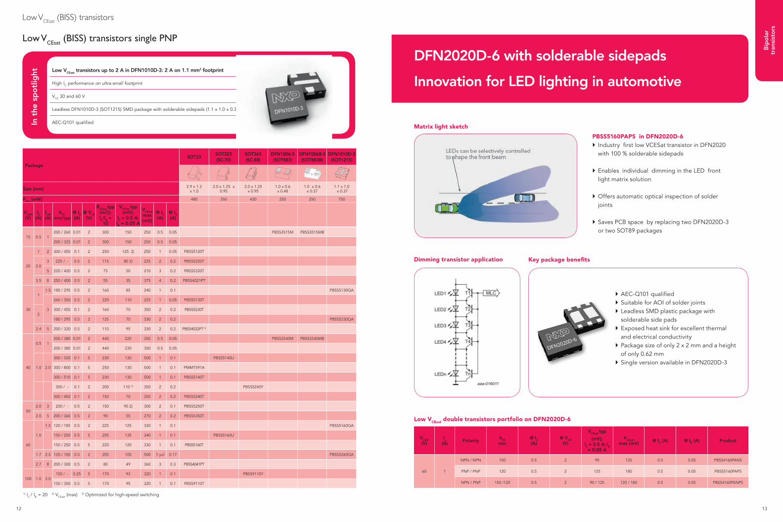
DFN2020D-6 with solderable sidepads
Innovation for LED lighting in automotive
Key package benefits
Matrix light sketch
Dimming transistor application
Low VCEsat double transistors portfolio on DFN2020D-6
Low VCEsat (BISS) transistors
Low VCEsat transistors up to 2 A in DFN1010D-3: 2 A on 1.1 mm2 footprint
High IC performance on ultra-small footprint
VCE 30 and 60 V
Leadless DFN1010D-3 (SOT1215) SMD package with solderable sidepads (1.1 x 1.0 x 0.37)
AEC-Q101 qualifiedIn t
he s
po
tlig
htLow VCEsat (BISS) transistors single PNP
Package
SOT23SOT323 (SC-70)
SOT363 (SC-88)
DFN1006-3 (SOT883)
DFN1006B-3 (SOT883B)
DFN1010D-3(SOT1215)
Size (mm) 2.9 x 1.3 x 1.0
2.0 x 1.25 x 0.95
2.0 x 1.25 x 0.95
1.0 x 0.6 x 0.48
1.0 x 0.6 x 0.37
1.1 x 1.0 x 0.37
Ptot (mW) 480 350 430 250 250 750
VCEO
(V)IC
(A)ICM
(A)hFE
min/typ@ IC(A)
@ VCE
(V)
RCEsat typ (mΩ);IC/IB =
10
VCEsat typ (mV);
IC = 0.5 A;
IB = 0.05 A
VCEsat
max (mV)
@ IC(A)
@ IB(A)
15 0.5 1200 / 260 0.01 2 300 150 250 0.5 0.05 PBSS3515M PBSS3515MB
200 / 325 0.01 2 300 150 250 0.5 0.05
20
1 2 300 / 450 0.1 2 250 125 2) 250 1 0.05 PBSS5120T
2.03 225 / - 0.5 2 115 80 2) 225 2 0.2 PBSS5220T
5 220 / 420 0.5 2 75 50 210 3 0.2 PBSS5320T
3.5 8 250 / 400 0.5 2 55 35 375 4 0.2 PBSS4021PT
30
11.5 180 / 295 0.5 2 160 85 240 1 0.1 PBSS5130QA
3
260 / 350 0.5 2 220 110 225 1 0.05 PBSS5130T
2300 / 450 0.1 2 160 70 350 2 0.2 PBSS5230T
180 / 295 0.5 2 125 70 330 2 0.2 PBSS5230QA
2.4 5 200 / 320 0.5 2 110 95 330 2 0.2 PBSS4032PT 3)
40
0.5 1200 / 380 0.01 2 440 220 350 0.5 0.05 PBSS3540M PBSS3540MB
200 / 380 0.01 2 440 230 350 0.5 0.05
1.0 2.0
300 / 520 0.1 5 230 130 500 1 0.1 PBSS5140U
300 / 800 0.1 5 250 130 500 1 0.1 PMMT591A
300 / 510 0.1 5 230 130 500 1 0.1 PBSS5140T
300 / - 0.1 2 200 110 2) 350 2 0.2 PBSS5240Y
300 / 450 0.1 2 150 70 350 2 0.2 PBSS5240T
502.0 3 200 / - 0.5 2 150 90 2) 300 2 0.1 PBSS5250T
2.0 5 200 / 360 0.5 2 90 55 270 2 0.2 PBSS5350T
60
1.0
1.5 120 / 185 0.5 2 225 125 330 1 0.1 PBSS5160QA
150 / 250 0.5 5 255 135 340 1 0.1 PBSS5160U
150 / 250 0.5 5 220 120 330 1 0.1 PBSS5160T
1.7 2.5 120 / 185 0.5 2 205 105 500 1-juil 0.17 PBSS5260QA
2.7 8 200 / 300 0.5 2 80 49 360 3 0.3 PBSS4041PT
100 1.0 3.0150 / - 0.25 5 170 93 320 1 0.1 PBSS9110Y
150 / 350 0.5 5 170 95 320 1 0.1 PBSS9110T
1) IC / IB = 20 2) VCEsat (max) 3) Optimized for high-speed switching
M3D088
PBSS5160PAPS in DFN2020D-6 Industry first low VCESat transistor in DFN2020 with 100 % solderable sidepads
Enables individual dimming in the LED front light matrix solution
Offers automatic optical inspection of solder joints
Saves PCB space by replacing two DFN2020D-3 or two SOT89 packages
AEC-Q101 qualified Suitable for AOI of solder joints Leadless SMD plastic package with solderable side pads
Exposed heat sink for excellent thermal and electrical conductivity
Package size of only 2 x 2 mm and a height of only 0.62 mm
Single version available in DFN2020D-3
VCEO (V)
IC (A)
Polarity hFE min
@ IC (A)
@ VCE
(V)
VCEsat typ
(mV);IC = 0.5 A; IB
= 0.05 A
VCEsat
max (mV)@ IC (A) @ IB (A) Product
60 1
NPN / NPN 150 0.5 2 90 120 0.5 0.05 PBSS4160PANS
PNP / PNP 120 0.5 2 125 180 0.5 0.05 PBSS5160PAPS
NPN / PNP 150 /120 0.5 2 90 / 125 120 / 180 0.5 0.05 PBSS4160PANPS
14 15
Bip
ola
r tr
ansi
sto
rs
Medium-power low VCEsat (BISS) transistors single NPN
Low VCEsat (BISS) transistors
Package
SOT223 (SC-73)
SOT89 (SC-62)
SOT457 (SC-74)
DFN2020-3 (SOT1061)
DFN2020D-3(SOT1061D)
Size (mm) 6.5 x 3.5 x 1.65 4.5 x 2.5 x 1.5 2.9 x 1.5 x 1.0 2.0 x 2.0 x 0.62 2.0 x 2.0 x 0.62
Ptot (mW) 1700 1650 750 1300 1300
VCEO
(V)IC
(A)ICM
(A)hFE
min/typ@ IC(A)
@ VCE
(V)
RCEsat typ (mΩ);
IC/IB = 10
VCEsat typ (mV);
IC = 0.5 A;
IB = 0.05 A
VCEsat
max (mV)
@ IC(A)
@ IB(A)
12
5.3 10.6 300 / 530 0.5 2 27 1) 18 200 5.3 0.265 PBSS301NX
5.8 11.6 300 / 530 0.5 2 29 1) 18 235 5.8 0.29 PBSS301NZ
6 7 280 / 440 0.5 2 33 1) 20 275 6 0.3 PBSS4612PA PBSS4612PAS
20
3 5 220 / 390 0.5 2 85 40 310 3 0.3 PBSS4320X
4 15 300 / 450 0.5 2 50 30 280 4 0.4 PBSS301ND
5 10 300 / 450 0.5 2 32 35 220 5 0.5 PBSS4520X
5.3 10.6 300 / 570 0.5 2 27 1) 20 200 5.3 0.265 PBSS302NX
5.8 10.2 300 / 570 0.5 2 30 1) 20 250 5.8 0.29 PBSS302NZ
6 7 280 / 440 0.5 2 33 1) 20 275 6 0.3 PBSS4620PA PBSS4620PAS
7 15 300 / 550 0.5 2 19 12 210 7 0.35 PBSS4021NX
8 20 300 / 550 0.5 2 14 9 170 8 0.4 PBSS4021NZ
30
3 5 300 / 490 0.5 2 80 45 300 3 0.3 PBSS4330X
3 5 300 / 465 0.5 2 75 40 300 3 0.3 PBSS4330PA PBSS4330PAS
3.5 6 300 / 500 0.5 2 50 70 300 4 0.4 PBSS4032ND 3)
4.7 10 300 / 500 0.5 2 45 57 250 4 0.4 PBSS4032NX 3)
5.1 10.2 300 / 480 0.5 2 30 1) 20 220 5.1 0.255 PBSS303NX
5.4 10 300 / 500 0.5 2 45 57 340 4.9 0.27 PBSS4032NZ 3)
5.5 11 300 / 480 0.5 2 31 1) 20 240 5.5 0.275 PBSS303NZ
6 7 280 / 450 0.5 2 35 1) 21 275 6 0.3 PBSS4630PA PBSS4630PAS
40
2.0 3.0 300 / - 0.5 5 280 140 510 2 0.2 PBSS4240X
415 300 / 520 0.5 2 55 35 300 4 0.4 PBSS302ND
10 300 / 500 0.5 2 40 21 355 5 0.5 PBSS4540X
5 10 300 / 500 0.5 2 42 25 355 5 0.5 PBSS4540Z
50
2 5 300 / - 0.5 2 160 90 2) 320 2 0.2 PBSS4250X
3.0 5.0
200 / 280 0.5 2 110 65 290 2 0.2 PBSS4350D
300 / 460 0.5 2 75 50 370 3 0.3 PBSS4350X
200 / 280 0.5 2 110 60 1) 290 2 0.2 PBSS4350Z
60
3 6 345 / 570 0.5 2 65 40 260 3 0.3 PBSS303ND
4.7 9.4 300 / 520 0.5 2 37 1) 25 245 4.7 0.235 PBSS304NX
5.2 10.4 300 / 520 0.5 2 39 1) 25 280 5.2 0.26 PBSS304NZ
6 7 280 / 440 0.5 2 34 1) 22 290 6 0.3 PBSS4560PA PBSS4560PAS
6.2 15 300 / 500 0.5 2 25 17 230 6 0.3 PBSS4041NX
7 15 300 / 500 0.5 2 17.5 13 195 7 0.35 PBSS4041NZ
80
3 6 240 / 360 0.5 2 67 40 255 3 0.3 PBSS304ND
4 10 250 / 400 0.5 2 43 1) 25 230 4 0.2 PBSS4480X
4.6 9.2 300 / 470 0.5 2 37 1) 25 240 4.6 0.23 PBSS305NX
5.1 10.2 300 / 470 0.5 2 38 1) 25 270 5.1 0.255 PBSS305NZ
5.6 7 270 / 425 0.5 2 40 1) 25 320 5.6 0.28 PBSS4580PA PBSS4580PAS
100
150 / 290 0.25 10 160 75 200 1 0.1 PBSS8110D
150 / 290 0.25 10 165 73 200 1 0.1 PBSS8110X
150 / 290 0.25 10 160 73 200 1 0.1 PBSS8110Z
3 4 170 / 275 0.5 2 72 45 360 4 0.4 PBSS305ND
4.5 9 200 / 330 0.5 2 38 1) 27 245 4.5 0.225 PBSS306NX
5.1 10.2 200 / 330 0.5 2 43 1) 27 300 5.1 0.255 PBSS306NZ
5.2 6 180 / 285 0.5 2 48 1) 30 340 5.2 0.26 PBSS8510PA PBSS8510PAS
M3D109
types in bold represent new products
1) IC / IB = 20 2) VCEsat (max) 3) Optimized for high-speed switching
types in bold represent new products
Low VCEsat (BISS) transistors
Package
SOT96(SO8)
SOT457(SC-74)
SOT666 DFN2020-6(SOT1118)
DFN2020D-6(SOT1118D)
Size (mm) 4.9 x 3.9 x 1.75
2.9 x 1.5 x 1.0
1.6 x 1.2 x 0.55
2.0 x 2.0x 0.62
2.0 x 2.0 x 0.62
Ptot (mW) 2000 2) 750 500 1300 1300
VCEO
(V)IC
(A)Polarity hFE
min@ IC(A)
@ VCE
(V)
VCEsat typ (mV);
IC = 0.5 A;IB = 0.05 A
VCEsat
max (mV)
@ IC(A)
@ IB(A)
15 0.5
2 x NPN 200 0.01 2 170 1) 250 0.5 0.05 PBSS2515VS
2 x PNP 200 0.01 2 170 1) 250 0.5 0.05 PBSS3515VS
NPN / PNP 200 0.01 2 170 1) 250 0.5 0.05 PBSS2515VPN
NPN / PNP 200 0.01 2 170 1) 250 0.5 0.05
20
7.5 NPN / NPN 300 0.5 2 15 150 4 0.2 PBSS4021SN
6.3 PNP / PNP 250 0.5 2 24 225 4 0.2 PBSS4021SP
7.5 / 6.3 NPN / PNP 300 / 250 0.5 2 15 / 24 150 / 225 4 0.2 PBSS4021SPN
30
1
NPN / NPN 210 0.5 2 75 100 0.5 0.05 PBSS4130PAN
PNP / PNP 170 0.5 2 85 140 0.5 0.05 PBSS5130PAP
NPN / PNP 210 / 170 0.5 2 75 / 85 100 / 140 0.5 0.05 PBSS4130PANP
2
NPN / NPN 230 0.5 2 60 80 0.5 0.05 PBSS4230PAN
PNP / PNP 210 0.5 2 75 110 0.5 0.05 PBSS5230PAP
NPN / PNP 230 / 210 0.5 2 60 / 75 80 / 100 0.5 0.05 PBSS4230PANP
5.7 NPN / NPN 300 0.5 2 57 250 4 0.4 PBSS4032SN 3)
4.8 PNP / PNP 200 0.5 2 70 390 4 0.4 PBSS4032SP 3)
5.7 / 4.8 NPN / PNP 300 / 200 0.5 2 57 / 70 250 / 390 4 0.4 PBSS4032SPN 3)
401.0 NPN / PNP 300 / 250 0.5 5 130 / 150 500 1 0.1 PBSS4140DPN
2.0 NPN / PNP 300 / 250 0.5 5 80 / 100 400 / 530 2 0.2 PBSS4240DPN
50 2.7
2 x NPN 300 0.5 2 50 340 2.7 0.27 PBSS4350SS
2 x PNP 200 0.5 2 60 370 2.7 0.27 PBSS5350SS
NPN / PNP 300 / 200 0.5 2 50 / 60 340 / 370 2.7 0.27 PBSS4350SPN
60
1.0
2 x NPN 200 0.5 5 115 250 1 0.1 PBSS4160DS
2 x PNP 150 0.5 5 120 330 1 0.1 PBSS5160DS
NPN / PNP 200 / 150 0.5 5 115 / 120 250 / 330 1 0.1 PBSS4160DPN
1
NPN / NPN 150 0.5 2 90 120 0.5 0.05 PBSS4160PAN PBSS4160PANS
PNP / PNP 120 0.5 2 125 180 0.5 0.05 PBSS5160PAP PBSS5160PAPS
NPN / PNP 150 / 120 0.5 2 90 / 125 120 / 180 0.5 0.05 PBSS4160PANP PBSS4160PANPS
2
NPN / NPN 210 0.5 2 70 90 0.5 0.05 PBSS4260PAN
PNP / PNP 140 0.5 2 100 140 0.5 0.05 PBSS5260PAP
NPN / PNP 210 / 140 0.5 2 70 / 100 90 / 140 0.5 0.05 PBSS4260PANP
6.7 NPN / NPN 300 0.5 2 20 190 4 0.2 PBSS4041SN
5.9 PNP / PNP 200 0.5 2 35 330 4 0.2 PBSS4041SP
6.7 / 5.9 NPN / PNP 300 / 200 0.5 2 20 / 35 190 / 330 4 0.2 PBSS4041SPN
120 1
NPN / NPN 240 0.1 2 90 120 0.5 0.05 PBSS4112PAN
PNP / PNP 190 0.1 2 150 220 0.5 0.05 PBSS5112PAP
NPN / PNP 240 / 190 0.1 2 90 / 150 120 / 220 0.5 0.05 PBSS4112PANP
Low VCEsat (BISS) double transistors
1) Ic / Ib=20 2) Device mounted on a ceramic PCB, AI2O3, standard footprint 3) Optimized for high-speed switching
In t
he s
po
tlig
ht
Low VCEsat (BISS) transistors
Industry‘s first combination of reduced switching times (down to 125 ns) with minimized saturation voltage (below 50 mV)
Voltage range from 12 to 120 V
Flexible package options, from standard SMD to brand-new, ultra-small leadless package DFN1010B-3 (SOT883B) (1.0 x 0.6 x 0.37 mm)
Provides benchmark reduced on-state resistance
New double BISS transistors in LFPAK56D (SOT1205), DFN2020-6 (SOT1118), and DFN2020D-6 (SOT1118D) with solderable sidepads
New 2 A BISS transistors in SOT89 and SOT223 available: PBSS4240X, PBSS5240X, PBSS4240Z, and PBSS5240Z
16 17
Bip
ola
r tr
ansi
sto
rs
Package
SOT457 (SC-74)
SOT363 (SC-88)
Size (mm) 2.9 x 1.5 x 1.0 2.0 x 1.25 x 0.95
Ptot (mW) 750 1) 600 1) 300 2)
VCEO
(V)IC
(A)VCEsat max (mV); IC = 0.5 A;
IB = 0.05 AR1, R2 (kΩ)
15 0.5 250
2.2 PBLS1501Y
4.7 PBLS1502Y
10 PBLS1503Y
22 PBLS1504Y
20
1 150
2.2 PBLS2001D
4.7 PBLS2002D
10 PBLS2003D
22 PBLS2004D
1.8 70
2.2 PBLS2021D
4.7 PBLS2022D
10 PBLS2023D
22 PBLS2024D
40
0.5 350
2.2 PBLS4001Y
4.7 PBLS4002Y
10 PBLS4003Y
22 PBLS4004Y
47 PBLS4005Y
1 170
2.2 PBLS4001D
4.7 PBLS4002D
10 PBLS4003D
22 PBLS4004D
47 PBLS4005D
60
1 180
2.2 PBLS6001D
4.7 PBLS6002D
10 PBLS6003D
22 PBLS6004D
47 PBLS6005D
1.5 100
2.2 PBLS6021D
4.7 PBLS6022D
10 PBLS6023D
22 PBLS6024D
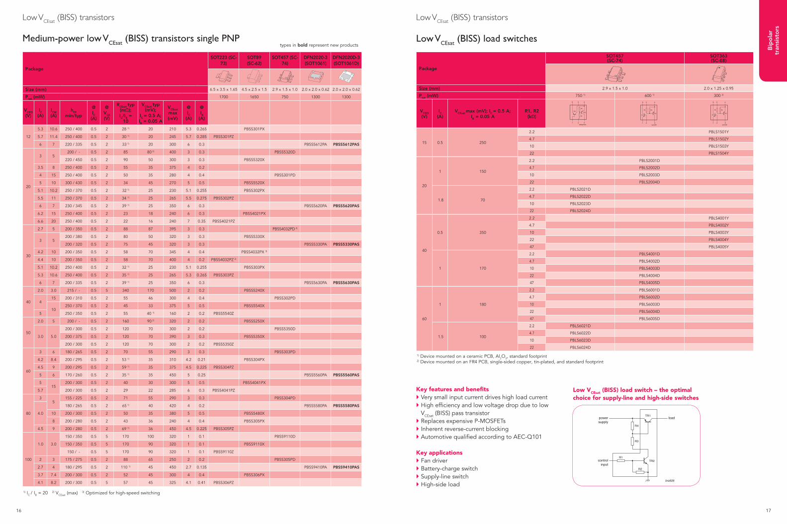
Low VCEsat (BISS) load switch – the optimal choice for supply-line and high-side switches
Low VCEsat (BISS) load switches
6 5 4
1 2 3
R2
TR1TR2
R1
sym036
6 5 4
1 2 3
R2
TR1TR2
R1
sym036
6 5 4
1 2 3
R2
TR1TR2
R1
006aab506
1) Device mounted on a ceramic PCB, Al2O3, standard footprint2) Device mounted on an FR4 PCB, single-sided copper, tin-plated, and standard footprint
Low VCEsat (BISS) transistors
Key features and benefits Very small input current drives high load current High efficiency and low voltage drop due to low
VCEsat (BISS) pass transistor Replaces expensive P-MOSFETs Inherent reverse-current blocking Automotive qualified according to AEC-Q101
Key applications Fan driver Battery-charge switch Supply-line switch High-side load
Medium-power low VCEsat (BISS) transistors single PNP
Low VCEsat (BISS) transistors
1) IC / IB = 20 2) VCEsat (max) 3) Optimized for high-speed switching
types in bold represent new products
Package
SOT223 (SC-73)
SOT89 (SC-62)
SOT457 (SC-74)
DFN2020-3 (SOT1061)
DFN2020D-3(SOT1061D)
Size (mm) 6.5 x 3.5 x 1.65 4.5 x 2.5 x 1.5 2.9 x 1.5 x 1.0 2.0 x 2.0 x 0.62 2.0 x 2.0 x 0.62
Ptot (mW) 1700 1650 750 1300 1300
VCEO
(V)IC
(A)ICM
(A)hFE
min/typ
@ IC
(A)
@ VCE
(V)
RCEsat typ (mΩ);IC/IB =
10
VCEsat typ (mV);
IC = 0.5 A;
IB = 0.05 A
VCEsat
max (mV)
@ IC
(A)
@ IB
(A)
12
5.3 10.6 250 / 400 0.5 2 28 1) 20 210 5.3 0.265 PBSS301PX
5.7 11.4 250 / 400 0.5 2 30 1) 20 245 5.7 0.285 PBSS301PZ
6 7 220 / 335 0.5 2 33 1) 20 300 6 0.3 PBSS5612PA PBSS5612PAS
20
3 5200 / - 0.5 2 85 80 2) 400 3 0.3 PBSS5320D
220 / 450 0.5 2 90 50 300 3 0.3 PBSS5320X
3.5 8 250 / 400 0.5 2 55 35 375 4 0.2
4 15 250 / 400 0.5 2 50 35 280 4 0.4 PBSS301PD
5 10 300 / 430 0.5 2 34 45 270 5 0.5 PBSS5520X
5.1 10.2 250 / 370 0.5 2 32 1) 25 230 5.1 0.255 PBSS302PX
5.5 11 250 / 370 0.5 2 34 1) 25 265 5.5 0.275 PBSS302PZ
6 7 230 / 345 0.5 2 39 1) 25 350 6 0.3 PBSS5620PA PBSS5620PAS
6.2 15 250 / 400 0.5 2 23 18 240 6 0.3 PBSS4021PX
6.6 20 250 / 400 0.5 2 22 16 240 7 0.35 PBSS4021PZ
30
2.7 5 200 / 350 0.5 2 88 87 395 3 0.3 PBSS4032PD 3)
3 5200 / 380 0.5 2 80 50 320 3 0.3 PBSS5330X
200 / 320 0.5 2 75 45 320 3 0.3 PBSS5330PA PBSS5330PAS
4.2 10 200 / 350 0.5 2 58 70 345 4 0.4 PBSS4032PX 3)
4.4 10 200 / 350 0.5 2 58 70 400 4 0.2 PBSS4032PZ 3)
5.1 10.2 250 / 400 0.5 2 32 1) 25 230 5.1 0.255 PBSS303PX
5.3 10.6 250 / 400 0.5 2 35 1) 25 265 5.3 0.265 PBSS303PZ
6 7 200 / 335 0.5 2 39 1) 25 350 6 0.3 PBSS5630PA PBSS5630PAS
40
2.0 3.0 215 / - 0.5 5 340 170 500 2 0.2 PBSS5240X
415 200 / 310 0.5 2 55 46 300 4 0.4 PBSS302PD
10250 / 370 0.5 2 45 33 375 5 0.5 PBSS5540X
5 250 / 350 0.5 2 55 40 1) 160 2 0.2 PBSS5540Z
50
2.0 5 200 / - 0.5 2 160 90 2) 320 2 0.2 PBSS5250X
3.0 5.0
200 / 300 0.5 2 120 70 300 2 0.2 PBSS5350D
200 / 375 0.5 2 120 70 390 3 0.3 PBSS5350X
200 / 300 0.5 2 120 70 300 2 0.2 PBSS5350Z
60
3 6 180 / 265 0.5 2 70 55 290 3 0.3 PBSS303PD
4.2 8.4 200 / 295 0.5 2 53 1) 35 310 4.2 0.21 PBSS304PX
4.5 9 200 / 295 0.5 2 59 1) 35 375 4.5 0.225 PBSS304PZ
5 6 170 / 260 0.5 2 35 1) 35 450 5 0.25 PBSS5560PA PBSS5560PAS
515
200 / 300 0.5 2 40 30 300 5 0.5 PBSS4041PX
5.7 200 / 300 0.5 2 29 22 285 6 0.3 PBSS4041PZ
80
35
155 / 225 0.5 2 71 55 290 3 0.3 PBSS304PD
4.0
180 / 265 0.5 2 65 1) 40 420 4 0.2 PBSS5580PA PBSS5580PAS
10 200 / 300 0.5 2 50 35 380 5 0.5 PBSS5480X
8 200 / 280 0.5 2 43 36 240 4 0.4 PBSS305PX
4.5 9 200 / 280 0.5 2 69 1) 36 450 4.5 0.225 PBSS305PZ
100
1.0 3.0
150 / 350 0.5 5 170 100 320 1 0.1 PBSS9110D
150 / 350 0.5 5 170 90 320 1 0.1 PBSS9110X
150 / - 0.5 5 170 90 320 1 0.1 PBSS9110Z
2 3 175 / 275 0.5 2 88 65 250 2 0.2 PBSS305PD
2.7 4 180 / 295 0.5 2 110 1) 45 450 2.7 0.135 PBSS9410PA PBSS9410PAS
3.7 7.4 200 / 300 0.5 2 52 45 300 4 0.4 PBSS306PX
4.1 8.2 200 / 300 0.5 5 57 45 325 4.1 0.41 PBSS306PZ
M3D109
18 19
Bip
ola
r tr
ansi
sto
rs
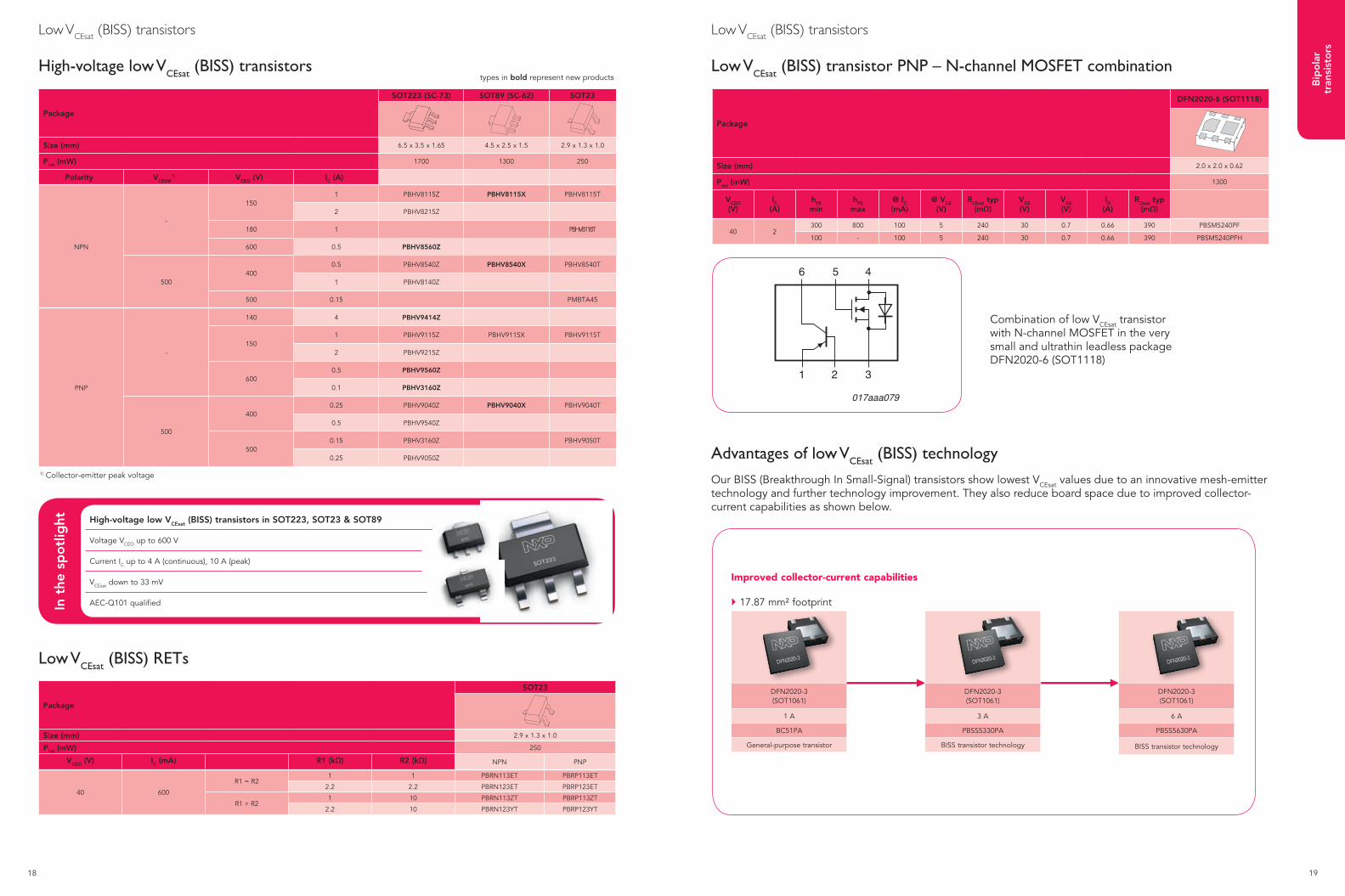
Our BISS (Breakthrough In Small-Signal) transistors show lowest VCEsat values due to an innovative mesh-emitter technology and further technology improvement. They also reduce board space due to improved collector- current capabilities as shown below.
Combination of low VCEsat transistor with N-channel MOSFET in the very small and ultrathin leadless package DFN2020-6 (SOT1118)
Advantages of low VCEsat (BISS) technology
Low VCEsat (BISS) transistors
Package
DFN2020-6 (SOT1118)
Size (mm) 2.0 x 2.0 x 0.62
Ptot (mW) 1300
VCEO
(V)IC
(A)hFE
minhFE
max@ IC(mA)
@ VCE
(V)RCEsat typ
(mΩ)VDS
(V)VGS
(V)ID
(A)RDson typ
(mΩ)
40 2300 800 100 5 240 30 0.7 0.66 390 PBSM5240PF
100 - 100 5 240 30 0.7 0.66 390 PBSM5240PFH
Low VCEsat (BISS) transistor PNP – N-channel MOSFET combination
017aaa079
6 5 4
1 2 3
DFN2020-3(SOT1061)
1 A
BC51PA
General-purpose transistor
Improved collector-current capabilities
17.87 mm² footprint
DFN2020-3 (SOT1061)
3 A
PBSS5330PA
BISS transistor technology
DFN2020-3 (SOT1061)
6 A
PBSS5630PA
BISS transistor technology
Package
SOT223 (SC-73) SOT89 (SC-62) SOT23
Size (mm) 6.5 x 3.5 x 1.65 4.5 x 2.5 x 1.5 2.9 x 1.3 x 1.0
Ptot (mW) 1700 1300 250
Polarity VCESM1) VCEO (V) IC (A)
NPN
-
1501 PBHV8115Z PBHV8115X PBHV8115T
2 PBHV8215Z
180 1 PBHV8118T
600 0.5 PBHV8560Z
500400
0.5 PBHV8540Z PBHV8540X PBHV8540T
1 PBHV8140Z
500 0.15 PMBTA45
PNP
-
140 4 PBHV9414Z
1501 PBHV9115Z PBHV9115X PBHV9115T
2 PBHV9215Z
6000.5 PBHV9560Z
0.1 PBHV3160Z
500
4000.25 PBHV9040Z PBHV9040X PBHV9040T
0.5 PBHV9540Z
5000.15 PBHV3160Z PBHV9050T
0.25 PBHV9050Z
Low VCEsat (BISS) transistors
1) Collector-emitter peak voltage
High-voltage low VCEsat (BISS) transistors
Low VCEsat (BISS) RETs
Package
SOT23
Size (mm) 2.9 x 1.3 x 1.0
Ptot (mW) 250
VCEO (V) IC (mA) R1 (kΩ) R2 (kΩ) NPN PNP
40 600
R1 = R21 1 PBRN113ET PBRP113ET
2.2 2.2 PBRN123ET PBRP123ET
R1 ≠ R21 10 PBRN113ZT PBRP113ZT
2.2 10 PBRN123YT PBRP123YT
M3D088
M3D088M3D109
types in bold represent new products
High-voltage low VCEsat (BISS) transistors in SOT223, SOT23 & SOT89
Voltage VCEO up to 600 V
Current IC up to 4 A (continuous), 10 A (peak)
VCEsat down to 33 mV
AEC-Q101 qualifiedIn t
he s
po
tlig
ht
20 21
Bip
ola
r tr
ansi
sto
rs
RETs 100 mA double
Resistor-equipped transistors (RETs)
Package
DFN1010B-6 (SOT1216)
SOT363(SC-88)
SOT666
Size (mm) 1.1 x 1.0 x 0.37 2.0 x 1.25 x 0.95 1.6 x 1.2 x 0.55
Ptot (mW) 350 300 300
VCEO (V) IC (mA) Configuration R1 (kΩ)
R2 (kΩ) NPN / PNP NPN / NPN NPN / PNP PNP / PNP NPN / NPN NPN / PNP PNP / PNP
50 100
R1 = R2
2.2 2.2 PUMH20 PUMD20 PUMB20 PEMH20 PEMD20 PEMB20
4.7 4.7 PUMH15 PUMD15 PUMB15 PEMH15 PEMD15 PEMB15
10 10 PUMH11 PUMD3 PUMB11 PEMH11 PEMD3 PEMB11
22 22 PUMH1 PUMD2 PUMB1 PEMH1 PEMD2 PEMB1
47 47 PQMD12 PUMH2 PUMD12 PUMB2 PEMH2 PEMD12 PEMB2
100 100 PUMH24 PUMD24 PUMB24 PEMH24 PEMD24 PEMB24
R1 ≠ R2
2.2 47 PUMH10 PUMD10 PUMB10 PEMH10 PEMD10 PEMB10
4.7 10 PUMH18 PUMD18 PUMB18 PEMH18 PEMD18 PEMB18
4.7 47 PUMH13 PUMD13 PUMB13 PEMH13 PEMD13 PEMB13
10 47 PUMH9 PUMD9 PUMB9 PEMH9 PEMD9 PEMB9
22 47 PUMH16 PUMD16 PUMB16 PEMH16 PEMD16 PEMB16
47 22 PUMH17 PUMD17 PUMB17 PEMH17 PEMD17 PEMB17
47 / 2.2 47 / 47 PUMD48 PEMD48
Only R1
2.2 - PUMH30 PUMD30 PUMB30 PEMH30 PEMD30 PEMB30
4.7 - PUMH7 PUMD6 PUMB3 PEMH7 PEMD6 PEMB3
10 - PUMH4 PUMD4 PUMB4 PEMH4 PEMD4 PEMB4
22 - PUMH19 PUMD19 PUMB19 PEMH19 PEMD19 PEMB19
47 - PUMH14 PUMD14 PUMB14 PEMH14 PEMD14 PEMB14
Package
SOT457 (SC-74) SOT23 SOT323 (SC-70)
Size (mm) 2.9 x 1.5 x 1.0 2.9 x 1.3 x 1.0 2.0 x 1.25 x 0.95
Ptot (mW) 750 250 200
VCEO (V) IC (mA) R1 (kΩ) R2 (kΩ) NPN / NPN
NPN /PNP NPN PNP NPN PNP
50 500
R1 = R2
1 1 PDTD113ET PDTB113ET PDTD113EU PDTB113EU
2.2 2.2 PDTD123ET PDTB123ET PDTD123EU PDTB123EU
4.7 4.7 PDTD143ET PDTB143ET PDTD143EU PDTB143EU
10 10 PDTD114ET PDTB114ET PDTD114EU PDTB114EU
R1 ≠ R2
1 10 PIMN31 PIMC31 PDTD113ZT PDTB113ZT PDTD113ZU PDTB113ZU
2.2 10 PDTD123YT PDTB123YT PDTD123YU PDTB123YU
4.7 10 PDTD143XT PDTB143XT PDTD143XU PDTB143XU
Only R1 2.2 - PDTD123TT PDTB123TT
RETs 500 mA
M3D088
types in bold represent new products
Resistor-equipped transistors (RETs)
RETs 100 mA single - Part 1
RETs 100 mA single - Part 2
Package
SOT23 SOT323 (SC-70)
Size (mm) 2.9 x 1.3 x 1.0 2.0 x 1.25 x 0.95
Ptot (mW) 250 200
VCEO (V) IC (mA) Configuration R1 (kΩ) R2 (kΩ) NPN PNP NPN PNP
50 100
1 1 PDTA113ET PDTA113EU
2.2 2.2 PDTC123ET PDTA123ET PDTC123EU PDTA123EU
4.7 4.7 PDTC143ET PDTA143ET PDTC143EU PDTA143EU
10 10 PDTC114ET PDTA114ET PDTC114EU PDTA114EU
22 22 PDTC124ET PDTA124ET PDTC124EU PDTA124EU
47 47 PDTC144ET PDTA144ET PDTC144EU PDTA144EU
100 100 PDTC115ET PDTA115ET PDTC115EU PDTA115EU
1 10 PDTA113ZT PDTA113ZU
2.2 10 PDTC123YT PDTA123YT PDTC123YU PDTA123YU
2.2 47 PDTC123JT PDTA123JT PDTC123JU PDTA123JU
4.7 10 PDTC143XT PDTA143XT PDTC143XU PDTA143XU
4.7 47 PDTC143ZT PDTA143ZT PDTC143ZU PDTA143ZU
10 47 PDTC114YT PDTA114YT PDTC114YU PDTA114YU
22 47 PDTC124XT PDTA124XT PDTC124XU PDTA124XU
47 10 PDTC144VT PDTA144VT PDTC144VU PDTA144VU
47 22 PDTC144WT PDTA144WT PDTC144WU PDTA144WU
2.2 - PDTC123TT PDTA123TT PDTC123TU PDTA123TU
4.7 - PDTC143TT PDTA143TT PDTC143TU PDTA143TU
10 - PDTC114TT PDTA114TT PDTC114TU PDTA114TU
22 - PDTC124TT PDTA124TT PDTC124TU PDTA124TU
47 - PDTC144TT PDTA144TT PDTC144TU PDTA144TU
100 - PDTC115TT PDTA115TT PDTC115TU PDTA115TU
Package
DFN1006-3 (SOT883) DFN1006B-3 (SOT883B)
Size (mm) 1.0 x 0.6 x 0.48 1.0 x 0.6 x 0.37
Ptot (mW) 250 250
VCEO (V) IC (mA) Configuration R1 (kΩ) R2 (kΩ) NPN PNP NPN PNP
50 100
1 1 PDTA113EM PDTA113EMB
2.2 2.2 PDTC123EM PDTA123EM PDTC123EMB PDTA123EMB
4.7 4.7 PDTC143EM PDTA143EM PDTC143EMB PDTA143EMB
10 10 PDTC114EM PDTA114EM PDTC114EMB PDTA114EMB
22 22 PDTC124EM PDTA124EM PDTC124EMB PDTA124EMB
47 47 PDTC144EM PDTA144EM PDTC144EMB PDTA144EMB
100 100 PDTC115EM PDTA115EM PDTC115EMB PDTA115EMB
1 10 PDTA113ZM PDTA113ZMB
2.2 10 PDTC123YM PDTA123YM PDTC123YMB PDTA123YMB
2.2 47 PDTC123JM PDTA123JM PDTC123JMB PDTA123JMB
4.7 10 PDTC143XM PDTA143XM PDTC143XMB PDTA143XMB
4.7 47 PDTC143ZM PDTA143ZM PDTC143ZMB PDTA143ZMB
10 47 PDTC114YM PDTA114YM PDTC114YMB PDTA114YMB
22 47 PDTC124XM PDTA124XM PDTC124XMB PDTA124XMB
47 10 PDTC144VM PDTA144VM PDTC144VMB PDTA144VMB
47 22 PDTC144WM PDTA144WM PDTC144WMB PDTA144WMB
2.2 - PDTC123TM PDTA123TM PDTC123TMB PDTA123TMB
4.7 - PDTC143TM PDTA143TM PDTC143TMB PDTA143TMB
10 - PDTC114TM PDTA114TM PDTC114TMB PDTA114TMB
22 - PDTC124TM PDTA124TM PDTC124TMB PDTA124TMB
47 - PDTC144TM PDTA144TM PDTC144TMB PDTA144TMB
100 - PDTC115TM PDTA115TM PDTC115TMB PDTA115TMB
M3D088
MSE187
R1
MSE187
R1
22 23
Bip
ola
r tr
ansi
sto
rs
Package
SOT457(SC-74)
SOT363(SC-88)
SOT666 DFN1010B-6(SOT1216)
Size (mm) 2.9 x 1.5 x 1.0 2.0 x 1.25 x 0.95 1.6 x 1.2 x 0.55 1.0 x 1.0 x 0.37
Ptot (mW) 750 300 300 350
Polarity VCEO (V) IC (mA) hFE min hFE max fT min (MHz)
NPN
40 100 120 450 100 PUMX1 PEMX1
45 100 200 450 100 BC847DS BC847BS BC847BV BC847QAS
65 100110 - 100 BC846S
200 450 100 BC846DS BC846BS
50 150 120 560 100 PUMX2
45 500 160 400 80 BC817DS
PNP
40 100 120 450 100 PIMT1 PUMT1 PEMT1
45 100 200 450 100 BC857BS BCC857BV BC857QAS
65 100110 - 100 BC856S
200 450 100 BC856BS
45 500 160 400 80 BC807DS
NPN / PNP
40 100 120 450 100 PUMZ1 PEMZ1
45 100 200 450 100 BC847BPN BC847BVN BC847QAPN
50 100 120 560 100 PIMZ2 PUMZ2
65 100 200 450 100 BC846BPN
12 500 200 - 250 / 100 PEMZ7
45 500 160 160 100 / 800 BC817DPN
Double transistors
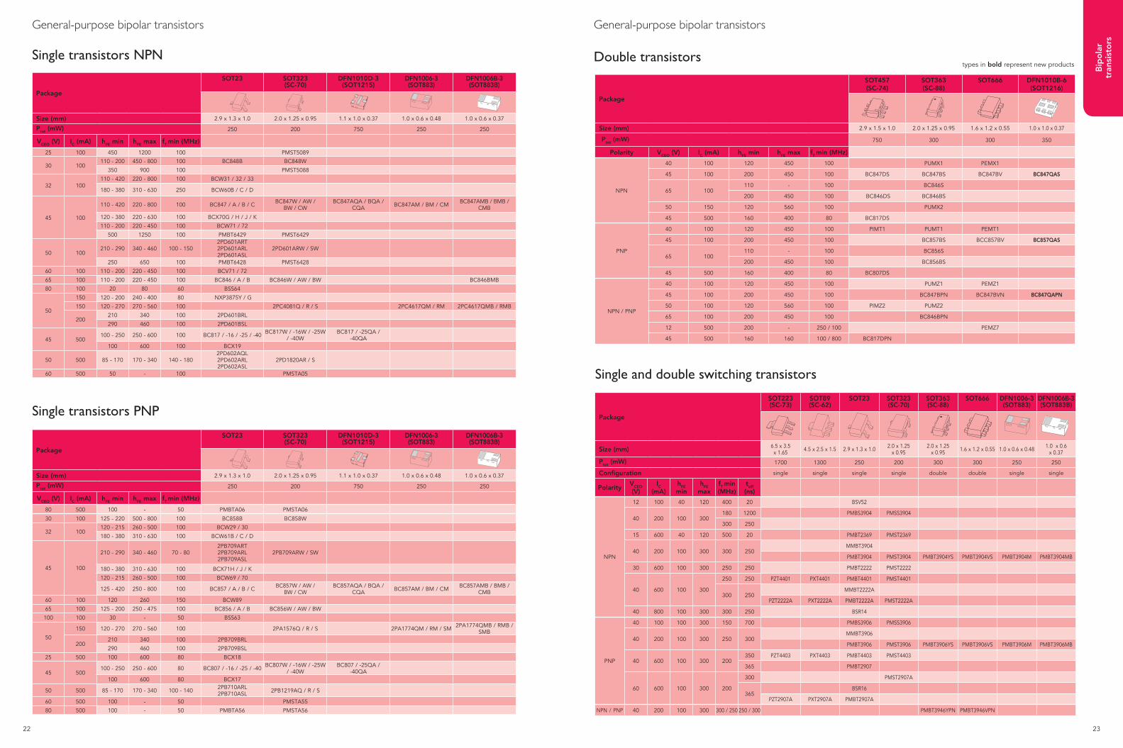
General-purpose bipolar transistors
Single and double switching transistors
Package
SOT223 (SC-73)
SOT89 (SC-62)
SOT23 SOT323 (SC-70)
SOT363 (SC-88)
SOT666 DFN1006-3 (SOT883)
DFN1006B-3 (SOT883B)
Size (mm) 6.5 x 3.5x 1.65 4.5 x 2.5 x 1.5 2.9 x 1.3 x 1.0 2.0 x 1.25
x 0.952.0 x 1.25
x 0.95 1.6 x 1.2 x 0.55 1.0 x 0.6 x 0.48 1.0 x 0.6 x 0.37
Ptot (mW) 1700 1300 250 200 300 300 250 250
Configuration single single single single double double single single
PolarityVCEO (V)
IC (mA)
hFE min
hFE max
fT min(MHz)
toff (ns)
NPN
12 100 40 120 400 20 BSV52
40 200 100 300180 1200 PMBS3904 PMSS3904
300 250
15 600 40 120 500 20 PMBT2369 PMST2369
40 200 100 300 300 250MMBT3904
PMBT3904 PMST3904 PMBT3904YS PMBT3904VS PMBT3904M PMBT3904MB
30 600 100 300 250 250 PMBT2222 PMST2222
40 600 100 300
250 250 PZT4401 PXT4401 PMBT4401 PMST4401
300 250MMBT2222A
PZT2222A PXT2222A PMBT2222A PMST2222A
40 800 100 300 300 250 BSR14
PNP
40 100 100 300 150 700 PMBS3906 PMSS3906
40 200 100 300 250 300MMBT3906
PMBT3906 PMST3906 PMBT3906YS PMBT3906VS PMBT3906M PMBT3906MB
40 600 100 300 200350 PZT4403 PXT4403 PMBT4403 PMST4403
365 PMBT2907
60 600 100 300 200
300 PMST2907A
365BSR16
PZT2907A PXT2907A PMBT2907A
NPN / PNP 40 200 100 300 300 / 250 250 / 300 PMBT3946YPN PMBT3946VPN
M3D109M3D088
types in bold represent new productsSingle transistors NPN
Single transistors PNP
General-purpose bipolar transistors
Package
SOT23 SOT323 (SC-70)
DFN1010D-3 (SOT1215)
DFN1006-3 (SOT883)
DFN1006B-3 (SOT883B)
Size (mm) 2.9 x 1.3 x 1.0 2.0 x 1.25 x 0.95 1.1 x 1.0 x 0.37 1.0 x 0.6 x 0.48 1.0 x 0.6 x 0.37
Ptot (mW) 250 200 750 250 250
VCEO (V) IC (mA) hFE min hFE max fT min (MHz)
25 100 450 1200 100 PMST5089
30 100110 - 200 450 - 800 100 BC848B BC848W
350 900 100 PMST5088
32 100110 - 420 220 - 800 100 BCW31 / 32 / 33
180 - 380 310 - 630 250 BCW60B / C / D
45 100
110 - 420 220 - 800 100 BC847 / A / B / C BC847W / AW / BW / CW
BC847AQA / BQA / CQA BC847AM / BM / CM BC847AMB / BMB /
CMB
120 - 380 220 - 630 100 BCX70G / H / J / K
110 - 200 220 - 450 100 BCW71 / 72
500 1250 100 PMBT6429 PMST6429
50 100210 - 290 340 - 460 100 - 150
2PD601ART2PD601ARL2PD601ASL
2PD601ARW / SW
250 650 100 PMBT6428 PMST6428
60 100 110 - 200 220 - 450 100 BCV71 / 72
65 100 110 - 200 220 - 450 100 BC846 / A / B BC846W / AW / BW BC846BMB
80 100 20 80 60 BSS64
50
150 120 - 200 240 - 400 80 NXP3875Y / G
150 120 - 270 270 - 560 100 2PC4081Q / R / S 2PC4617QM / RM 2PC4617QMB / RMB
200210 340 100 2PD601BRL
290 460 100 2PD601BSL
45 500100 - 250 250 - 600 100 BC817 / -16 / -25 / -40 BC817W / -16W / -25W
/ -40WBC817 / -25QA /
-40QA100 600 100 BCX19
50 500 85 - 170 170 - 340 140 - 1802PD602AQL2PD602ARL2PD602ASL
2PD1820AR / S
60 500 50 - 100 PMSTA05
Package
SOT23 SOT323 (SC-70)
DFN1010D-3 (SOT1215)
DFN1006-3 (SOT883)
DFN1006B-3 (SOT883B)
Size (mm) 2.9 x 1.3 x 1.0 2.0 x 1.25 x 0.95 1.1 x 1.0 x 0.37 1.0 x 0.6 x 0.48 1.0 x 0.6 x 0.37
Ptot (mW) 250 200 750 250 250
VCEO (V) IC (mA) hFE min hFE max fT min (MHz)
80 500 100 - 50 PMBTA06 PMSTA06
30 100 125 - 220 500 - 800 100 BC858B BC858W
32 100120 - 215 260 - 500 100 BCW29 / 30
180 - 380 310 - 630 100 BCW61B / C / D
45 100
210 - 290 340 - 460 70 - 802PB709ART2PB709ARL2PB709ASL
2PB709ARW / SW
180 - 380 310 - 630 100 BCX71H / J / K
120 - 215 260 - 500 100 BCW69 / 70
125 - 420 250 - 800 100 BC857 / A / B / C BC857W / AW / BW / CW
BC857AQA / BQA / CQA BC857AM / BM / CM BC857AMB / BMB /
CMB60 100 120 260 150 BCW89
65 100 125 - 200 250 - 475 100 BC856 / A / B BC856W / AW / BW
100 100 30 - 50 BSS63
50
150 120 - 270 270 - 560 100 2PA1576Q / R / S 2PA1774QM / RM / SM 2PA1774QMB / RMB /SMB
200210 340 100 2PB709BRL
290 460 100 2PB709BSL
25 500 100 600 80 BCX18
45 500100 - 250 250 - 600 80 BC807 / -16 / -25 / -40 BC807W / -16W / -25W
/ -40WBC807 / -25QA /
-40QA100 600 80 BCX17
50 500 85 - 170 170 - 340 100 - 140 2PB710ARL2PB710ASL 2PB1219AQ / R / S
60 500 100 - 50 PMSTA55
80 500 100 - 50 PMBTA56 PMSTA56
M3D088
M3D088
24 25
Bip
ola
r tr
ansi
sto
rs
LED driver
General-purpose bipolar transistors
Package
SOT457
Size (mm) 2.9 x 1.5 x 1.0
Ptot (mW) 750
Vs supply voltage [V] LED drive current [mA] @ Vs=10V
40
10 NCR401U
20 NCR402U
50 NCR405U
Key features and benefits Single-chip constant-current source with reduced
component count Output current set by an external resistor Very small footprint for smaller designs
Key applications Constant-current LED driver Generic constant-current source Active bias control for audio amplifiers
Key features and benefits Single-chip constant-current source with reduced
component count Very small footprint for smaller designs
Key applications Constant-current LED driver Generic constant-current source Active bias control for audio amplifiers
Voltage reference
Voltage reference
Constant-current source
Package
SOT353 (SC-88A)
Size (mm) 2.0 x 1.25 x 0.95
Ptot (mW) 335
Type PSSI2021SAY
Description maximum supply voltage
maximum supply current
typical stabilized output current
minimum stabilized output current
maximum stabilized output current
typical load stability of stabilized output
current
typical output current change over ambient
temperature
Parameter VS max (V) IS max (mA) Iout typ (µA) Iout min (mA) Iout max (mA) ∆Iout/Iout typ (%) ∆Iout/(Iout*∆Tamb
)
typ (%/K)
Value 75 2.2 15 0.015 50 0.5 0.15
General-purpose bipolar transistors
Medium-power general-purpose transistors
1) Typical value
High voltage transistors
For high-voltage transistors with increased performance please refer to our high-voltage low VCEsat (BISS) transistor portfolio on page 18.
Package
SOT223 (SC-73) SOT89 (SC-62) SOT457 (SC-74) SOT23 SOT323 (SC-70)
Size (mm) 6.5 x 3.5 x 1.65 4.5 x 2.5 x 1.5 2.9 x 1.5 x 1.0 2.9 x 1.3 x 1.0 2.0 x 1.25 x 0.95
Ptot (mW) 1700 1300 750 250 200
Polarity VCEO (V) IC (mA) hFE min hFE max fT min (MHz)
NPN
80 100 20 - 60 BSS64
140 300 60 250 100 PMBT5550 PMST5550
160 300 80 250 100 PMBT5551/BSR19A PMST5551
250 100 50 - 60 BF722 BF622 BF822
300 10050 - 60 BF720 BF620 BF820 BF820W
40 - 50 PZTA42 PXTA42 PMBTA42 PMSTA42
350 100 40 - 70 BSP19 BST39
400 300 50 200 20 PZTA44 PMBTA44
PNP
100 100 30 - 50 BSS63
250 10050 - 60 BF723
50 - 60 BF623 BF823
300 10050 - 60 BF621 BF821
40 - 50 PZTA92 PXTA92 PMBTA92 PMSTA92
2 x NPN 300 100 40 - 50 PMBTA42DS
M3D109 M3D088
In t
he S
po
tlig
ht Medium-power transistors in DFN2020-3 and DFN2020D-3 (with solderable sidepads)
Excellent electrical perfomance on a small 2 x 2 mm footprint
80% board space reduction (DFN2020 vs. SOT89)
100% solderable sidepads (DFN2020D-3)
VCEO ranging from 20 to 80 V
High collector-current capability IC up to 2 A
AEC-Q101 qualifiedIn t
he s
po
tlig
httypes in bold represent new products
Package
SOT223 (SC-73) SOT89 (SC-62) DFN2020-3 (SOT1061) DFN2020D-3 (SOT1061D)
Size (mm) 6.5 x 3.5 x 1.65 4.5 x 2.5 x 1.5 2.0 x 2.0 x 0.62 2.0 x 2.0 x 0.62
Ptot (mW) 1700 1300 1300 1300
Polarity VCEO (V) IC (A) hFE min hFE max fT min (MHz)
NPN
20 2 85 - 160 375 40 BCP68 / -25 BC868 / -25 BC68PA / BC68-25PA BC68PAS / BC68-25PAS
45 1 63 - 100 160 - 250 100 BCP54 / -10 / -16 BCX54 / -10 / -16 BC54PA / BC54-10PA / BC54-16PA
BC54PAS / BC54-10PAS / BC54-16PAS
60 163 - 100 160 - 250 100 BCP55 / -10 / -16 BCX55 / -10 / -16 BC55PA / BC55-10PA /
BC55-16PABC55PAS / BC55-10PAS /
BC55-16PAS
100 300 100 BSP41 BSR41
80 163 - 100 160 - 250 100 BCP56 / -10 / -16 BCX56 / -10 / -16 BC56PA / BC56-10PA /
BC56-16PABC56PAS / BC56-10PAS /
BC56-16PAS
40 - 100 120 - 300 100 BSP43 BSR43
PNP
20 2 85 - 160 250 - 375 40 BCP69 / -16 / -25 BC869 / -16 / -25 BC69PA / BC69-16PA / BC69-25PA
BC69PAS / BC569-16PAS / BC69-25PAS
45 1 63 - 100 160 - 250 115 1) - 145 1) BCP51 / -10 / -16 BCX51 / -10 / -16 BC51PA / BC51-10PA / BC51-16PA
BC51PAS / BC51-10PAS / BC51-16PAS
60 163 - 100 160 - 250 100 BCP52 / -10 / -16 BCX52 / -10 / -16 BC52PA / BC52-10PA /
BC52-16PABC52PAS / BC52-10PAS /
BC52-16PAS
40 - 100 120 - 300 100 BSP31 BSR30 / 31
80 163 - 100 160 - 250 115 1) - 145 1) BCP53 / -10 / -16 BCX53 / -10 / -16 BC53PA / BC53-10PA /
BC53-16PABC53PAS / BC53-10PAS /
BC53-16PAS
40 - 100 120 - 300 100 BSP32 / 33 BSR33
M3D109
26 27
Bip
ola
r tr
ansi
sto
rs
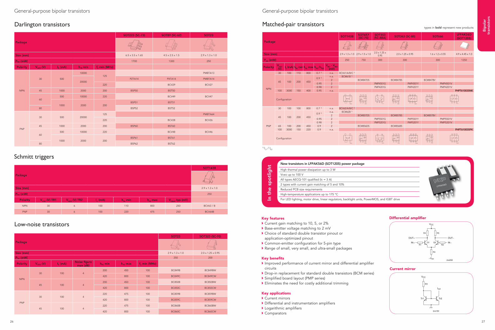
General-purpose bipolar transistors
Key features Current gain matching to 10, 5, or 2% Base-emitter voltage matching to 2 mV Choice of standard double transistor pinout or
application-optimized pinout Common-emitter configuration for 5-pin type Range of small, very small, and ultra-small packages
Key benefits Improved performance of current mirror and differential amplifier
circuits Drop-in replacement for standard double transistors (BCM series) Simplified board layout (PMP series) Eliminates the need for costly additional trimming
Key applications Current mirrors Differential and instrumentation amplifiers Logarithmic amplifiers Comparators
Differential amplifier
Current mirror
Package
SOT143B SOT457 (SC-74)
SOT353 (SC-88A) SOT363 (SC-88) SOT666
LFPAK56D (SOT1205)
Size (mm) 2.9 x 1.3 x 1.0 2.9 x 1.5 x 1.0 2.0 x 1.25 x 0.95 2.0 x 1.25 x 0.95 1.6 x 1.2 x 0.55 4.9 x 4.45 x 1.0
Ptot (mW) 250 750 300 300 300 1250
PolarityVCEO (V)
IC (mA) hFE min hFE max hFE1/hFE2
VBE1 - VBE2 (mV)
NPN
30 100 110 800 0.7 1) n.a. BCV61/A/B/C 1)
45 100 200 4500.9 1)
n.a. BCM61B 1)
2 BCM847DS BCM847BS BCM847BV0.95 2 PMP4501G PMP4501Y PMP4501V0.98 2 PMP4201G PMP4201Y PMP4201V
100 3000 150 400 0.95 n.a. PHPT610035NK
Configuration
PNP
30 100 100 800 0.7 1) n.a. BCV62/A/B/C 1)
45 100 200 4500.9 1)
n.a. BCM62B 1)
2 BCM857DS BCM857BS BCM857BV0.95 2 PMP5501G PMP5501Y PMP5501V0.98 2 PMP5201G PMP5201Y PMP5201V
65 100 200 450 0.9 2 BCM856DS BCM856BS100 3000 150 220 0.9 n.a. PHPT610035PK
Configuration
Matched-pair transistors
1) IC1 / IE2
New transistors in LFPAK56D (SOT1205) power package
High thermal power dissipation up to 3 W
Vceo up to 100 V
All types AECQ-101 qualified (Ic = 3 A)
2 types with current gain matching of 5 and 10%
Reduced PCB size requirements
High-temperature applications up to 175 °C
For LED lighting, motor drive, linear regulators, backlight units, PowerMOS, and IGBT driveIn t
he s
po
tlig
ht
types in bold represent new products
Package
SOT223 (SC-73) SOT89 (SC-62) SOT23
Size (mm) 6.5 x 3.5 x 1.65 4.5 x 2.5 x 1.5 2.9 x 1.3 x 1.0
Ptot (mW) 1700 1300 250
Polarity VCEO (V) IC (mA) hFE min fT min (MHz)
NPN
30 500
10000125
PMBTA13
20000PZTA14 PXTA14 PMBTA14
220 BCV29 BCV27
45 1000 2000 200 BSP50 BST50
60500 10000 220 BCV49 BCV47
1000 2000 200BSP51 BST51
80 BSP52 BST52
PNP
30 500 20000125 PMBTA64
220 BCV28 BCV26
45 1000 2000 200 BSP60 BST60
60500 10000 220 BCV48 BCV46
1000 2000 200BSP61 BST61
80 BSP62 BST62
General-purpose bipolar transistors
Package
SOT143B
Size (mm) 2.9 x 1.3 x 1.0
Ptot (mW) 250
Polarity VCEO (V) TR1 VCEO (V) TR2 IC (mA) hFE min hFE max VCEsat typ (mV)
NPN 30 6 100 110 800 250 BCV63 / B
PNP 30 6 100 220 475 250 BCV64B
Schmitt triggers
Darlington transistors
M3D109 M3D088
Low-noise transistors
Package
SOT23 SOT323 (SC-70)
Size (mm) 2.9 x 1.3 x 1.0 2.0 x 1.25 x 0.95
Ptot (mW) 250 200
Polarity VCEO (V) IC (mA)Noise figure
max (dB)hFE min hFE max fT min (MHz)
NPN
30 100 4200 450 100 BC849B BC849BW
420 800 100 BC849C BC849CW
45 100 4200 450 100 BC850B BC850BW
420 800 100 BC850C BC850CW
PNP
30 100 4220 475 100 BC859B BC859BW
420 800 100 BC859C BC859CW
45 100 4220 475 100 BC860B BC860BW
420 800 100 BC860C BC860CW
M3D088
28 29
Medium-frequency transistors
Package
SOT23 SOT323 (SC-70)
Size (mm) 2.9 x 1.3 x 1.0 2.0 x 1.25 x 0.95
Ptot (mW) 250 200
Polarity VCEO (V) IC (mA) hFE min hFE max fT typ (MHz)
NPN
15 100
40
- 500 BF570
20
25 85 >275 BFS20 BFS20W
30 65 225 260 BFS19
40 25 67 220 380 BF840
PNP
30
25
25 50 250 BF824 BF824W
40 50 - >325 BF550
M3D088
General-purpose bipolar transistors
MOSFET driver
Key features and benefits Three different configurations Types available with standard, switching, and low
VCEsat (BISS) transistors Small footprint
Key applications Power management
- (Half) bridge push-pull driver- Isolated DC/DC converters- Secondary synchronous rectification
Peripheral driver- (Half) bridge push-pull driver- Motor driver- Brushless DC motor driver- Op-amp output current booster
Op-amp boosterMOSFET driver for faster switching, lower losses
VCEO (V)
IC (mA)
Icm [A]
Type Package Remark Configuration
30 0.1 0.2 BCV65
SOT143B
General-purpose transistors
40
0.6 1 PMD2001DSOT457 Switching transistors with
reduced storage time
1 2 PMD3001D Low VCEsat
Diodes
Schottky barrier diodes and rectifiers 31Medium-power low VF Schottky rectifiers single ≥1 A - Flatpower packages 31Medium-power low VF Schottky rectifiers single ≥100 mA - DSN packages 32Medium-power low VF Schottky rectifiers single ≥200 mA - leadless (DFN) packages 33Medium-power low VF Schottky rectifiers single ≥200 mA - leaded packages 34Medium-power low VF Schottky rectifiers dual ≥200 mA 35General-purpose Schottky diodes ≤250 mA 36Low-capacitance Schottky diodes 37
Zener diodes 38General-purpose Zener diodes 38Zener diodes specifications 39
Switching diodes 40General-purpose, high-speed switching diodes < 90 V 40General-purpose, high-speed switching diodes 100 V 40General-purpose, switching diodes ≥100 V 41PN-rectifier 41Controlled-avalanche switching diodes 42Low-leakage current-switching diodes 42
Power diodes 43Hyperfast power diodes 43Power Schottky diodes 43Casco diodes 43Ultrafast power diodes 44
30 31
Dio
des
types in bold represent new products
Schottky barrier diodes and rectifiers
I F m
ax (A
)
VR
max
(V)
VF
max
(mV
)
@ I F
max
I R m
ax (m
A)
@ V
R m
ax
Package
CFP15 (SOT1289)
CFP5 (SOD128)
CFP3 (SOD123W)
Size (mm) 5.8 x 4.3 x 0.78 3.8 x 2.5 x 1.0 2.6 x 1.7 x 1.0
Ptot (mW) @ 1 cm² 2150 1050 950
Optimization
1
20340 1 Low VF PMEG2010ER
450 0.05 Low IR PMEG2010BER
30360 1.5 Low VF PMEG3010EP PMEG3010ER
450
0.05
Low IR PMEG3010BEP PMEG3010BER
40 490Low VF PMEG4010EP PMEG4010ER
Low VF PMEG4010ETP PMEG4010ETR
60
5300.06
Low VF PMEG6010EP PMEG6010ER
530 Low VF PMEG6010ETR
660 0.0003 Low IR PMEG6010ELR
100 770 0.00015 Low IR PMEG10010ELR
2
30
360 3 Low VF PMEG3020EP
420 1.5 Low VF PMEG3020CEP PMEG3020ER
450 0.1 Low IR PMEG3020BEP
520 0.05 Low IR PMEG3020DEP PMEG3020BER
40 490 0.1Low VF PMEG4020EP PMEG4020ER
Low VF PMEG4020ETP PMEG4020ETR
60
530 0.2Low VF PMEG6020EP PMEG6020ER
Low VF PMEG6020ETP PMEG6020ETR
680 0.0007 Low IR PMEG6020AELP PMEG6020AELR
7600.0003
Low IR PMEG6020ELR
100770 Low IR PMEG10020AELP PMEG10020AELR
830 0.00015 Low IR PMEG10020ELR
3
30360 5 Low VF PMEG3030EP
450 0.15 Low IR PMEG3030BEP
40490 0.2
Low VF PMEG4030EP
Low VF PMEG4030ETP
540 0.1 Low IR PMEG4030ER
60
530 0.2 Low VF PMEG6030EP
475 0.4 Low VF PMEG6030EVP
530 0.2 Low VF PMEG6030ETP
690 0.001 LLow IR PMEG6030ELP
100 770 0.00045 Low IR PMEG10030ELP
4.5 60 530 0.4 Low VF PMEG6045ETP
5
30360 8 Low VF PMEG3050EP
450 0.25 Low IR PMEG3050BEP
40490 0.3
Low VF PMEG4050EP
Low VF PMEG4050ETP
45 Low VF PMEG045V050EPD
60 560 0.4 Low VF PMEG060V050EPD
1045
490 0.6Low VF PMEG045V1000EPD
Low VF PMEG45U10EPD
540 0.5 Low IR PMEG45A10EPD
60 560 0.7 Low VF PMEG060V100EPD
1545 490
0.03 Low IR PMEG045T150EPD
1Low VF PMEG045V150EPD
50 500 Low VF PMEG050V150EPD
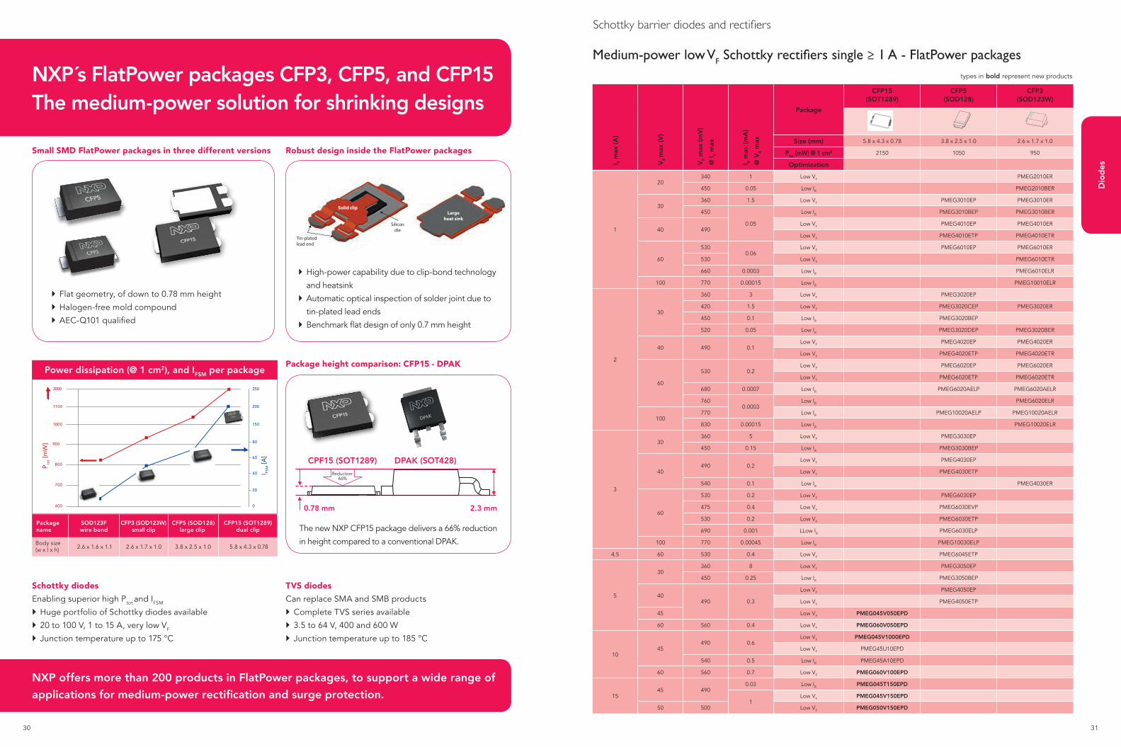
Medium-power low VF Schottky rectifiers single ≥ 1 A - FlatPower packages
NXP´s FlatPower packages CFP3, CFP5, and CFP15The medium-power solution for shrinking designs
Schottky diodes
Enabling superior high Ptot and IFSM
Huge portfolio of Schottky diodes available
20 to 100 V, 1 to 15 A, very low VF
Junction temperature up to 175 °C
TVS diodes
Can replace SMA and SMB products
Complete TVS series available
3.5 to 64 V, 400 and 600 W
Junction temperature up to 185 °C
The new NXP CFP15 package delivers a 66% reduction
in height compared to a conventional DPAK.
High-power capability due to clip-bond technology
and heatsink
Automatic optical inspection of solder joint due to
tin-plated lead ends
Benchmark flat design of only 0.7 mm height
NXP offers more than 200 products in FlatPower packages, to support a wide range of
applications for medium-power rectification and surge protection.
Flat geometry, of down to 0.78 mm height
Halogen-free mold compound
AEC-Q101 qualified
Small SMD FlatPower packages in three different versions
Package height comparison: CFP15 - DPAK
Robust design inside the FlatPower packages
Power dissipation (@ 1 cm2), and IFSM per package
Package name
SOD123Fwire bond
CFP3 (SOD123W)small clip
CFP5 (SOD128)large clip
Body size (w x l x h) 2.6 x 1.6 x 1.1 2.6 x 1.7 x 1.0 3.8 x 2.5 x 1.0
CFP15 (SOT1289)dual clip
5.8 x 4.3 x 0.78
600
700
800
900
1000 150
1100
2000
200
250
80
60
40
20
0
I FSM [A
]
Pto
t [m
W]
Reduction:66%
CPF15 (SOT1289)
0.78 mm 2.3 mm
DPAK (SOT428)
Tin-platedlead end
Silicondie
Solid clip
Large heat sink
Tin-platedlead end
Silicondie
Solid clip
Large heat sink
32 33
Dio
des
Schottky barrier diodes and rectifiers
types in bold represent new products
types in bold represent new products
I F m
ax (A
)
VR
max
(V)
VF
max
(mV
)
@ I F
max
I R m
ax (m
A)
@ V
R m
ax
Package
DSN0603-2(SOD962)
DSN1006-2(SOD993)
DSN1006U-2(SOD995)
Size (mm) 0.6 x 0.3 x 0.3 1.0 x 0.6 x 0.28 1.0 x 0.6 x 0.28
Ptot (mW) @ 1 cm² 525 tbd tbd
Optimization
0.1 12 250 2 Low VF PMEG1201AESF
0.2
20420 0.045 Low VF PMEG2002AESF
490 0.0035 Low IR PMEG2002ESF
30470 0.08 Low VF PMEG3002AESF
535 0.009 Low IR PMEG3002ESF
40525 0.08 Low VF PMEG4002AESF
600 0.0065 Low IR PMEG4002ESF
0.5
20550 0.045 Low VF PMEG2005AESF
620 0.0035 Low IR PMEG2005ESF
30630 0.08 Low VF PMEG3005AESF
720 0.009 Low IR PMEG3005ESF
40820 0.08 Low VF PMEG4005AESF
880 0.0065 Low IR PMEG4005ESF
130 typ. 415 typ. 0.3 Low VF PMEG3010AESB PMEG3010AESA
40 typ. 435 typ. 0.325 Low VF PMEG4010AESB
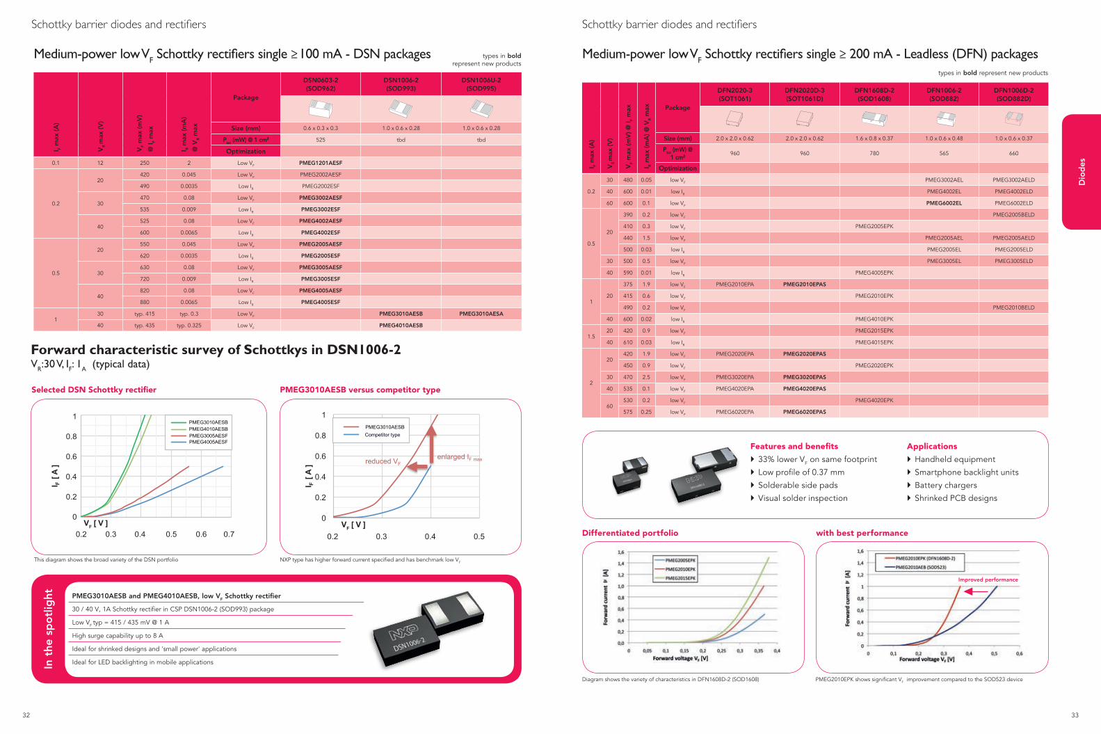
Medium-power low VF Schottky rectifiers single ≥ 100 mA - DSN packages
Schottky barrier diodes and rectifiers
Medium-power low VF Schottky rectifiers single ≥ 200 mA - Leadless (DFN) packages
I F m
ax (A
)
VR
max
(V)
VF
max
(mV
) @ I F
max
I R m
ax (m
A) @
VR m
ax Package
DFN2020-3(SOT1061)
DFN2020D-3(SOT1061D)
DFN1608D-2(SOD1608)
DFN1006-2(SOD882)
DFN1006D-2(SOD882D)
Size (mm) 2.0 x 2.0 x 0.62 2.0 x 2.0 x 0.62 1.6 x 0.8 x 0.37 1.0 x 0.6 x 0.48 1.0 x 0.6 x 0.37
Ptot (mW) @ 1 cm²
960 960 780 565 660
Optimization
0.2
30 480 0.05 low VF PMEG3002AEL PMEG3002AELD
40 600 0.01 low IR PMEG4002EL PMEG4002ELD
60 600 0.1 low VF PMEG6002EL PMEG6002ELD
0.5
20
390 0.2 low VF PMEG2005BELD
410 0.3 low VF PMEG2005EPK
440 1.5 low VF PMEG2005AEL PMEG2005AELD
500 0.03 low IR PMEG2005EL PMEG2005ELD
30 500 0.5 low VF PMEG3005EL PMEG3005ELD
40 590 0.01 low IR PMEG4005EPK
120
375 1.9 low VF PMEG2010EPA PMEG2010EPAS
415 0.6 low VF PMEG2010EPK
490 0.2 low VF PMEG2010BELD
40 600 0.02 low IR PMEG4010EPK
1.520 420 0.9 low VF PMEG2015EPK
40 610 0.03 low IR PMEG4015EPK
2
20420 1.9 low VF PMEG2020EPA PMEG2020EPAS
450 0.9 low VF PMEG2020EPK
30 470 2.5 low VF PMEG3020EPA PMEG3020EPAS
40 535 0.1 low VF PMEG4020EPA PMEG4020EPAS
60530 0.2 low VF PMEG4020EPK
575 0.25 low VF PMEG6020EPA PMEG6020EPAS
PMEG3010AESB and PMEG4010AESB, low VF Schottky rectifier
30 / 40 V, 1A Schottky rectifier in CSP DSN1006-2 (SOD993) package
Low VF typ = 415 / 435 mV @ 1 A
High surge capability up to 8 A
Ideal for shrinked designs and 'small power' applications
Ideal for LED backlighting in mobile applicationsIn t
he s
po
tlig
ht
Features and benefits
33% lower VF on same footprint
Low profile of 0.37 mm
Solderable side pads
Visual solder inspection
Applications
Handheld equipment
Smartphone backlight units
Battery chargers
Shrinked PCB designs
Improved performance
Differentiated portfolio with best performance
Diagram shows the variety of characteristics in DFN1608D-2 (SOD1608) PMEG2010EPK shows significant VF improvement compared to the SOD523 device
Forward characteristic survey of Schottkys in DSN1006-2VR:30 V, IF: 1A (typical data)
0
0.2
0.4
0.6
0.8
1
0.2 0.3 0.4 0.5
PMEG3010AESB PMEG4010AESB PMEG3005AESF PMEG4005AESF
PMEG3010AESB Competitor type
enlarged IF max reduced VF
I F [
A ]
I F [
A ]
VF [ V ] VF [ V ] 0
0.2
0.2 0.3 0.4 0.5 0.6 0.7
0.4
0.6
0.8
1
0
0.2
0.4
0.6
0.8
1
0.2 0.3 0.4 0.5
PMEG3010AESB PMEG4010AESB PMEG3005AESF PMEG4005AESF
PMEG3010AESB Competitor type
enlarged IF max reduced VF
I F [
A ]
I F [
A ]
VF [ V ] VF [ V ] 0
0.2
0.2 0.3 0.4 0.5 0.6 0.7
0.4
0.6
0.8
1
Selected DSN Schottky rectifier PMEG3010AESB versus competitor type
This diagram shows the broad variety of the DSN portfolio NXP type has higher forward current specified and has benchmark low VF
34 35
Dio
des
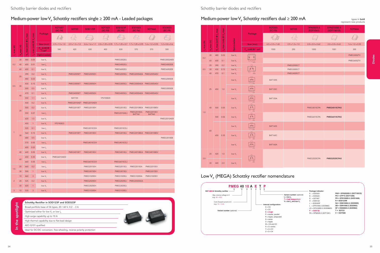
Low VF (MEGA) Schottky rectifier nomenclature
PAS = DFN2020D-3 (SOT1061D)PD = CFP15 (SOT1289)PK = DFN1608D-2 (SOD1608)R = SOD123WSA = DSN1006U-2 (SOD995)SB = DSN1006-2 (SOD993)SF = DSN0603-2 (SOD962)T = SOT23V = SOT666
Schottky barrier diodes and rectifiers
Medium-power low VF Schottky rectifiers dual ≥ 200 mA types in bold represent new products
I F m
ax (A
)
VR
max
(V)
VF
max
(mV
) @ I F
max
I R m
ax (m
A) @
VR m
ax
Op
tim
izat
ion
Package
SOT223(SC-73)
SOT23DFN2020-3 (SOT1061)
DFN2020D-3(SOT1061D)
SOT666
Size (mm) 6.5 x 3.5 x 1.65 2.9 x 1.3 x 1.0 2.0 x 2.0 x 0.62 2.0 x 2.0 x 0.63 1.6 x 1.2 x 0.55
Ptot (mW) @ 1 cm² 1500 250 1000 1001 300
0.230 480 0.03 low VF PMEG3002TV
60 600 0.1 low VF PMEG6002TV
0.5
20 390 0.2 low VF PMEG2005CT
30 430 0.15 low VF PMEG3005CT
40 470 0.1 low VF PMEG4005CT
1.0
25 450 1.0
low VF BAT120S
low VF BAT120C
low VF BAT120A
40 500 0.05 low VF PMEG4010CPA PMEG4010CPAS
60
540 0.06 low VF PMEG6010CPA PMEG6010CPAS
650 0.35
low VF BAT160S
low VF BAT160C
low VF BAT160A
2.0
20 420 1.0 low VF
PMEG2020CPA PMEG2020CPAS
30 440 2.0 low VF
M3D088
brb127
brb125
brb148
brb148
brb149
brb150
brb150
brb125
brb125
brb125
brb125
Schottky barrier diodes and rectifiers
Medium-power low VF Schottky rectifiers single ≥ 200 mA - Leaded packagesI F
max
(A)
VR
max
(V)
VF
max
(mV
) @ I F
max
I R m
ax (m
A) @
VR m
ax Package
SOT457(SC-74)
SOT23 SOD123FSOT323(SC-70)
SOD323F(SC-90)
SOD323(SC-76)
SOT666SOD523(SC-79)
Size (mm) 2.9 x 1.5 x 1.0 2.9 x 1.3 x 1.0 2.6 x 1.6 x 1.1 2.0 x 1.25 x 0.95 1.7 x 1.25 x 0.7 1.7 x 1.25 x 0.95 1.6 x 1.2 x 0.55 1.2 x 0.8 x 0.6
Ptot (mW) @ 1 cm²
540 420 830 400 830 570 570 500
Optimization
0.2
30 480 0.05 low VF PMEG3002EJ PMEG3002AEB
40 600 0.01 low IR PMEG4002EJ PMEG4002EB
60 600 0.1 low VF PMEG6002EJ PMEG6002EB
0.5
20390 0.2 low VF PMEG2005ET PMEG2005EH PMEG2005EJ PMEG2005AEA PMEG2005AEV
480 0.03 low IR PMEG2005EB
30430 0.15 low VF PMEG3005ET PMEG3005EH PMEG3005EJ PMEG3005AEA PMEG3005AEV
500 0.5 low VF PMEG3005EB
40470 0.1 low VF PMEG4005ET PMEG4005EH PMEG4005EJ PMEG4005AEA PMEG4005AEV
550 1.1 low VF BAT720 1PS70SB20
1
20
430 0.2 low VF PMEG2010AET PMEG2010AEH
500 0.2 low VF PMEG2010ET PMEG2010EH PMEG2010EJ PMEG2010BEA PMEG2010BEV
550 0.07 low IR PMEG2010AEJ PMEG2010EA BAT760
PMEG2010EV BAT960
620 1.5 low VF PMEG2010AEB
30
450 1 low VF 1PS74SB23
520 0.1 low IR PMEG3010CEH PMEG3010CEJ
560 0.15 low VF PMEG3010ET PMEG3010EH PMEG3010EJ PMEG3010BEA PMEG3010BEV
680 0.5 low VF PMEG3010EB
570 0.05 low IR PMEG4010CEH PMEG4010CEJ
600 0.02 low IR
40 640 0.05 low VF PMEG4010ET PMEG4010EH PMEG4010EJ PMEG4010BEA PMEG4010BEV
60650 0.35 low VF PMEG6010AED
660 0.05 low IR PMEG6010CEH PMEG6010CEJ
1.520 660 0.2 low IR PMEG2015EH PMEG2015EJ PMEG2015EA PMEG2015EV
30 500 1 low VF PMEG3015EH PMEG3015EJ PMEG3015EV
2
10 460 3 low VF PMEG1020EH PMEG1020EJ PMEG1020EA PMEG1020EV
20 525 0.2 low VF PMEG2020EH PMEG2020EJ PMEG2020AEA
30 620 1 low VF PMEG3020EH PMEG3020EJ
3 10 530 3 low VF PMEG1030EH PMEG1030EJ
M3D088
Schottky Rectifier in SOD123F and SOD323F
Broad portfolio base of 36 types, 20 / 60 V, 0.2 - 3 A
Optimized either for low VF or low IR
High surge capability up to 10 A
High thermal capability due to flat-lead design
AEC-Q101 qualified
Ideal for DC/DC conversion, free-wheeling, reverse polarity protectionIn t
he s
po
tlig
ht
36 37
Dio
des
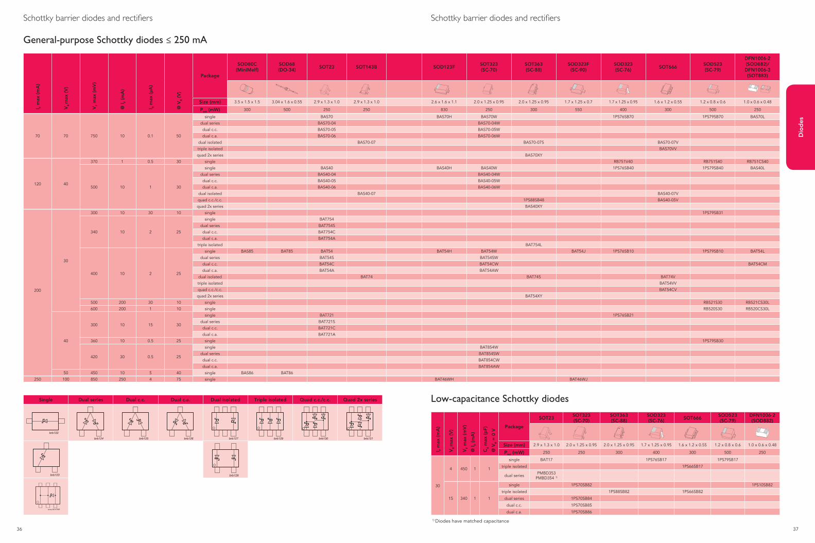
Schottky barrier diodes and rectifiers Schottky barrier diodes and rectifiers
General-purpose Schottky diodes ≤ 250 mAI F
max
(mA
)
VR
max
(V)
VF
max
(mV
)
@ I F
(mA
)
I R m
ax (μ
A)
@ V
R (V
)
Package
SOD80C(MiniMelf)
SOD68(DO-34)
SOT23 SOT143B SOD123FSOT323(SC-70)
SOT363(SC-88)
SOD323F(SC-90)
SOD323(SC-76)
SOT666SOD523(SC-79)
DFN1006-2 (SOD882)/ DFN1006-3 (SOT883)
Size (mm) 3.5 x 1.5 x 1.5 3.04 x 1.6 x 0.55 2.9 x 1.3 x 1.0 2.9 x 1.3 x 1.0 2.6 x 1.6 x 1.1 2.0 x 1.25 x 0.95 2.0 x 1.25 x 0.95 1.7 x 1.25 x 0.7 1.7 x 1.25 x 0.95 1.6 x 1.2 x 0.55 1.2 x 0.8 x 0.6 1.0 x 0.6 x 0.48
Ptot (mW) 300 500 250 250 830 250 300 550 400 300 500 250
70 70 750 10 0.1 50
single BAS70 BAS70H BAS70W 1PS76SB70 1PS79SB70 BAS70L
dual series BAS70-04 BAS70-04W
dual c.c. BAS70-05 BAS70-05W
dual c.a. BAS70-06 BAS70-06W
dual isolated BAS70-07 BAS70-07S BAS70-07V
triple isolated BAS70VV
quad 2x series BAS70XY
120 40
370 1 0.5 30 single RB751V40 RB751S40 RB751CS40
500 10 1 30
single BAS40 BAS40H BAS40W 1PS76SB40 1PS79SB40 BAS40L
dual series BAS40-04 BAS40-04W
dual c.c. BAS40-05 BAS40-05W
dual c.a. BAS40-06 BAS40-06W
dual isolated BAS40-07 BAS40-07V
quad c.c./c.c. 1PS88SB48 BAS40-05V
quad 2x series BAS40XY
200
30
300 10 30 10 single 1PS79SB31
340 10 2 25
single BAT754
dual series BAT754S
dual c.c. BAT754C
dual c.a. BAT754A
triple isolated BAT754L
400 10 2 25
single BAS85 BAT85 BAT54 BAT54H BAT54W BAT54J 1PS76SB10 1PS79SB10 BAT54L
dual series BAT54S BAT54SW
dual c.c. BAT54C BAT54CW BAT54CM
dual c.a. BAT54A BAT54AW
dual isolated BAT74 BAT74S BAT74V
triple isolated BAT54VV
quad c.c./c.c. BAT54CV
quad 2x series BAT54XY
500 200 30 10 single RB521S30 RB521CS30L
600 200 1 10 single RB520S30 RB520CS30L
40
300 10 15 30
single BAT721 1PS76SB21
dual series BAT721S
dual c.c. BAT721C
dual c.a. BAT721A
360 10 0.5 25 single 1PS79SB30
420 30 0.5 25
single BAT854W
dual series BAT854SW
dual c.c. BAT854CW
dual c.a. BAT854AW
50 450 10 5 40 single BAS86 BAT86
250 100 850 250 4 75 single BAT46WH BAT46WJ
M3D
050
M3D088
Single Dual series Dual c.c. Dual c.a. Dual isolated Triple isolated Quad c.c./c.c. Quad 2x series
brb122
brb124 brb125 brb126 brb127 brb129 brb130 brb131
brb123 brb128
Low-capacitance Schottky diodes
I F m
ax (m
A)
VR
max
(V)
VF
max
(mV
)
@ I F
(mA
)
Cd m
ax (p
F)
@ V
R =
0 V
Package
SOT23 SOT323(SC-70)
SOT363(SC-88)
SOD323(SC-76) SOT666 SOD523
(SC-79)DFN1006-2 (SOD882)
Size (mm) 2.9 x 1.3 x 1.0 2.0 x 1.25 x 0.95 2.0 x 1.25 x 0.95 1.7 x 1.25 x 0.95 1.6 x 1.2 x 0.55 1.2 x 0.8 x 0.6 1.0 x 0.6 x 0.48
Ptot (mW) 250 250 300 400 300 500 250
30
4 450 1 1
single BAT17 1PS76SB17 1PS79SB17
triple isolated 1PS66SB17
dual series PMBD353 PMBD354 1)
15 340 1 1
single 1PS70SB82 1PS10SB82
triple isolated 1PS88SB82 1PS66SB82
dual series 1PS70SB84
dual c.c. 1PS70SB85
dual c.a. 1PS70SB86
M3D088
1) Diodes have matched capacitance
38 39
Dio
des
Zener diodesZener diodes
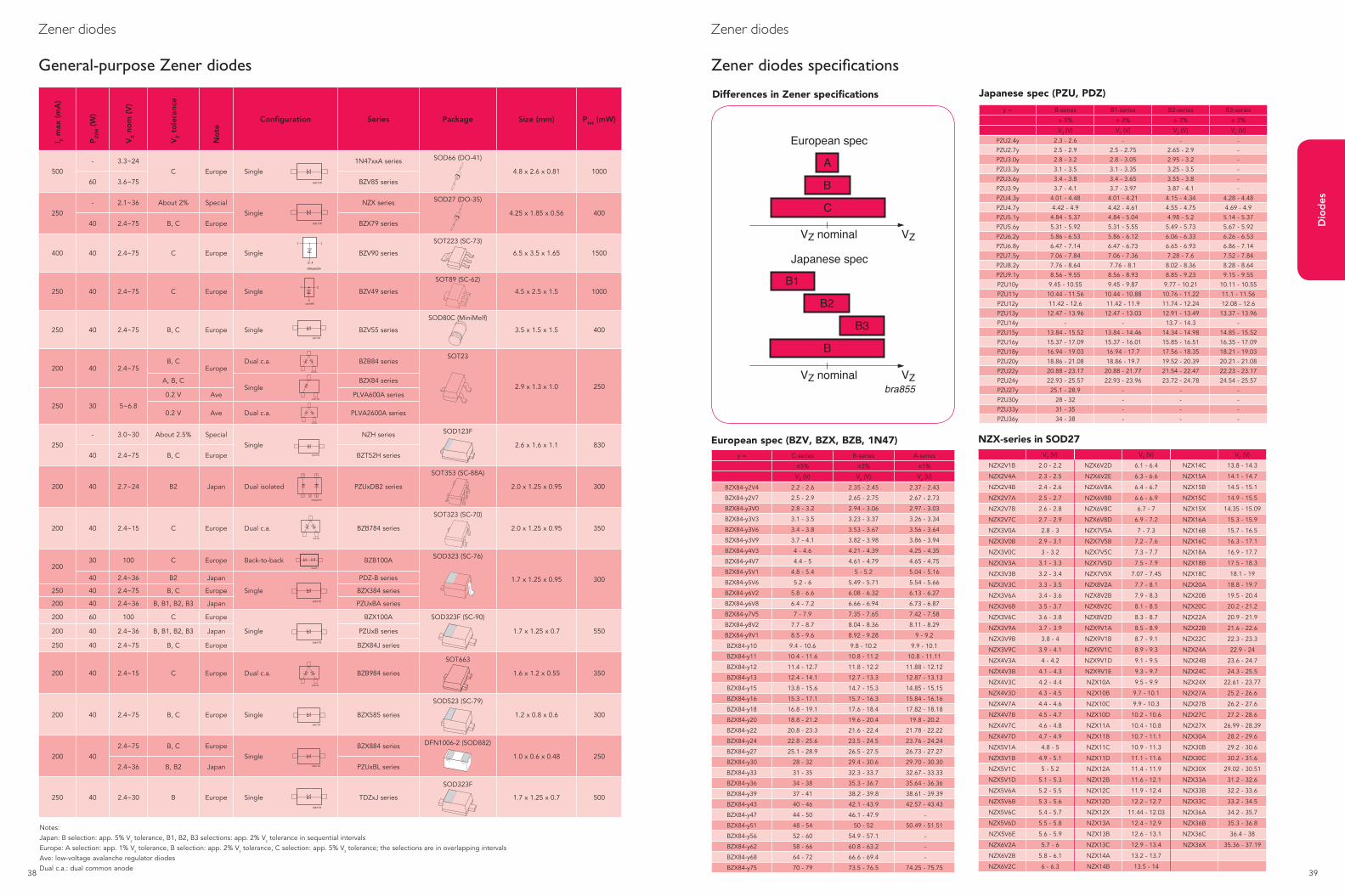
General-purpose Zener diodes Zener diodes specifications
Notes:Japan: B selection: app. 5% Vz tolerance, B1, B2, B3 selections: app. 2% Vz tolerance in sequential intervalsEurope: A selection: app. 1% Vz tolerance, B selection: app. 2% Vz tolerance, C selection: app. 5% Vz tolerance; the selections are in overlapping intervalsAve: low-voltage avalanche regulator diodesDual c.a.: dual common anode
I F m
ax (
mA
)
PZ
SM (
W)
VZ n
om
(V
)
VZ t
ole
ranc
e
No
te
Configuration Series Package Size (mm) Ptot (mW)
500
- 3.3~24
C Europe Single
1N47xxA series SOD66 (DO-41)
4.8 x 2.6 x 0.81 1000
60 3.6~75 BZV85 series
250
- 2.1~36 About 2% Special
Single
NZX series SOD27 (DO-35)
4.25 x 1.85 x 0.56 400
40 2.4~75 B, C Europe BZX79 series
400 40 2.4~75 C Europe Single BZV90 series
SOT223 (SC-73)
6.5 x 3.5 x 1.65 1500
250 40 2.4~75 C Europe Single BZV49 series
SOT89 (SC-62)
4.5 x 2.5 x 1.5 1000
250 40 2.4~75 B, C Europe Single BZV55 series
SOD80C (MiniMelf)
3.5 x 1.5 x 1.5 400
200 40 2.4~75B, C
EuropeDual c.a. BZB84 series
SOT23
2.9 x 1.3 x 1.0 250A, B, C
SingleBZX84 series
250 30 5~6.8
0.2 V Ave PLVA600A series
0.2 V Ave Dual c.a. PLVA2600A series
250
- 3.0~30 About 2.5% Special
Single
NZH series SOD123F
2.6 x 1.6 x 1.1 830
40 2.4~75 B, C Europe BZT52H series
200 40 2.7~24 B2 Japan Dual isolated PZUxDB2 series
SOT353 (SC-88A)
2.0 x 1.25 x 0.95 300
200 40 2.4~15 C Europe Dual c.a. BZB784 series
SOT323 (SC-70)
2.0 x 1.25 x 0.95 350
20030 100 C Europe Back-to-back BZB100A
SOD323 (SC-76)
1.7 x 1.25 x 0.95 30040 2.4~36 B2 Japan
Single
PDZ-B series
250 40 2.4~75 B, C Europe BZX384 series
200 40 2.4~36 B, B1, B2, B3 Japan PZUxBA series
200 60 100 C Europe
Single
BZX100A SOD323F (SC-90)
1.7 x 1.25 x 0.7 550200 40 2.4~36 B, B1, B2, B3 Japan PZUxB series
250 40 2.4~75 B, C Europe BZX84J series
200 40 2.4~15 C Europe Dual c.a. BZB984 series
SOT663
1.6 x 1.2 x 0.55 350
200 40 2.4~75 B, C Europe Single BZX585 series
SOD523 (SC-79)
1.2 x 0.8 x 0.6 300
200 40
2.4~75 B, C Europe
Single
BZX884 series DFN1006-2 (SOD882)
1.0 x 0.6 x 0.48 250
2.4~36 B, B2 Japan PZUxBL series
250 40 2.4~30 B Europe Single TDZxJ series
SOD323F
1.7 x 1.25 x 0.7 500
006aab234
2, 4
1 3
006aab219
1 3
5 4
2
brb118
brb118
brb118
brb118
brb118
brb118
brb118
brb118
brb118
sym0962
31
brb119
brb120
brb120
brb120
brb120
mse211
M3D130
M3D176
M3D109
M3D088
Differences in Zener specifications
y = C-series B-series A-series
±5% ±2% ±1%
VZ (V) VZ (V) VZ (V)
BZX84-y2V4 2.2 - 2.6 2.35 - 2.45 2.37 - 2.43
BZX84-y2V7 2.5 - 2.9 2.65 - 2.75 2.67 - 2.73
BZX84-y3V0 2.8 - 3.2 2.94 - 3.06 2.97 - 3.03
BZX84-y3V3 3.1 - 3.5 3.23 - 3.37 3.26 - 3.34
BZX84-y3V6 3.4 - 3.8 3.53 - 3.67 3.56 - 3.64
BZX84-y3V9 3.7 - 4.1 3.82 - 3.98 3.86 - 3.94
BZX84-y4V3 4 - 4.6 4.21 - 4.39 4.25 - 4.35
BZX84-y4V7 4.4 - 5 4.61 - 4.79 4.65 - 4.75
BZX84-y5V1 4.8 - 5.4 5 - 5.2 5.04 - 5.16
BZX84-y5V6 5.2 - 6 5.49 - 5.71 5.54 - 5.66
BZX84-y6V2 5.8 - 6.6 6.08 - 6.32 6.13 - 6.27
BZX84-y6V8 6.4 - 7.2 6.66 - 6.94 6.73 - 6.87
BZX84-y7V5 7 - 7.9 7.35 - 7.65 7.42 - 7.58
BZX84-y8V2 7.7 - 8.7 8.04 - 8.36 8.11 - 8.29
BZX84-y9V1 8.5 - 9.6 8.92 - 9.28 9 - 9.2
BZX84-y10 9.4 - 10.6 9.8 - 10.2 9.9 - 10.1
BZX84-y11 10.4 - 11.6 10.8 - 11.2 10.8 - 11.11
BZX84-y12 11.4 - 12.7 11.8 - 12.2 11.88 - 12.12
BZX84-y13 12.4 - 14.1 12.7 - 13.3 12.87 - 13.13
BZX84-y15 13.8 - 15.6 14.7 - 15.3 14.85 - 15.15
BZX84-y16 15.3 - 17.1 15.7 - 16.3 15.84 - 16.16
BZX84-y18 16.8 - 19.1 17.6 - 18.4 17.82 - 18.18
BZX84-y20 18.8 - 21.2 19.6 - 20.4 19.8 - 20.2
BZX84-y22 20.8 - 23.3 21.6 - 22.4 21.78 - 22.22
BZX84-y24 22.8 - 25.6 23.5 - 24.5 23.76 - 24.24
BZX84-y27 25.1 - 28.9 26.5 - 27.5 26.73 - 27.27
BZX84-y30 28 - 32 29.4 - 30.6 29.70 - 30.30
BZX84-y33 31 - 35 32.3 - 33.7 32.67 - 33.33
BZX84-y36 34 - 38 35.3 - 36.7 35.64 - 36.36
BZX84-y39 37 - 41 38.2 - 39.8 38.61 - 39.39
BZX84-y43 40 - 46 42.1 - 43.9 42.57 - 43.43
BZX84-y47 44 - 50 46.1 - 47.9 -
BZX84-y51 48 - 54 50 - 52 50.49 - 51.51
BZX84-y56 52 - 60 54.9 - 57.1 -
BZX84-y62 58 - 66 60.8 - 63.2 -
BZX84-y68 64 - 72 66.6 - 69.4 -
BZX84-y75 70 - 79 73.5 - 76.5 74.25 - 75.75
y = B-series B1-series B2-series B3-series
± 5% ± 2% ± 2% ± 2%
VZ (V) VZ (V) VZ (V) VZ (V)
PZU2.4y 2.3 - 2.6 - - -
PZU2.7y 2.5 - 2.9 2.5 - 2.75 2.65 - 2.9 -
PZU3.0y 2.8 - 3.2 2.8 - 3.05 2.95 - 3.2 -
PZU3.3y 3.1 - 3.5 3.1 - 3.35 3.25 - 3.5 -
PZU3.6y 3.4 - 3.8 3.4 - 3.65 3.55 - 3.8 -
PZU3.9y 3.7 - 4.1 3.7 - 3.97 3.87 - 4.1 -
PZU4.3y 4.01 - 4.48 4.01 - 4.21 4.15 - 4.34 4.28 - 4.48
PZU4.7y 4.42 - 4.9 4.42 - 4.61 4.55 - 4.75 4.69 - 4.9
PZU5.1y 4.84 - 5.37 4.84 - 5.04 4.98 - 5.2 5.14 - 5.37
PZU5.6y 5.31 - 5.92 5.31 - 5.55 5.49 - 5.73 5.67 - 5.92
PZU6.2y 5.86 - 6.53 5.86 - 6.12 6.06 - 6.33 6.26 - 6.53
PZU6.8y 6.47 - 7.14 6.47 - 6.73 6.65 - 6.93 6.86 - 7.14
PZU7.5y 7.06 - 7.84 7.06 - 7.36 7.28 - 7.6 7.52 - 7.84
PZU8.2y 7.76 - 8.64 7.76 - 8.1 8.02 - 8.36 8.28 - 8.64
PZU9.1y 8.56 - 9.55 8.56 - 8.93 8.85 - 9.23 9.15 - 9.55
PZU10y 9.45 - 10.55 9.45 - 9.87 9.77 - 10.21 10.11 - 10.55
PZU11y 10.44 - 11.56 10.44 - 10.88 10.76 - 11.22 11.1 - 11.56
PZU12y 11.42 - 12.6 11.42 - 11.9 11.74 - 12.24 12.08 - 12.6
PZU13y 12.47 - 13.96 12.47 - 13.03 12.91 - 13.49 13.37 - 13.96
PZU14y - - 13.7 - 14.3 -
PZU15y 13.84 - 15.52 13.84 - 14.46 14.34 - 14.98 14.85 - 15.52
PZU16y 15.37 - 17.09 15.37 - 16.01 15.85 - 16.51 16.35 - 17.09
PZU18y 16.94 - 19.03 16.94 - 17.7 17.56 - 18.35 18.21 - 19.03
PZU20y 18.86 - 21.08 18.86 - 19.7 19.52 - 20.39 20.21 - 21.08
PZU22y 20.88 - 23.17 20.88 - 21.77 21.54 - 22.47 22.23 - 23.17
PZU24y 22.93 - 25.57 22.93 - 23.96 23.72 - 24.78 24.54 - 25.57
PZU27y 25.1 - 28.9 - - -
PZU30y 28 - 32 - - -
PZU33y 31 - 35 - - -
PZU36y 34 - 38 - - -
European spec (BZV, BZX, BZB, 1N47)
Japanese spec (PZU, PDZ)
VZ (V) VZ (V) VZ (V)
NZX2V1B 2.0 - 2.2 NZX6V2D 6.1 - 6.4 NZX14C 13.8 - 14.3
NZX2V4A 2.3 - 2.5 NZX6V2E 6.3 - 6.6 NZX15A 14.1 - 14.7
NZX2V4B 2.4 - 2.6 NZX6V8A 6.4 - 6.7 NZX15B 14.5 - 15.1
NZX2V7A 2.5 - 2.7 NZX6V8B 6.6 - 6.9 NZX15C 14.9 - 15.5
NZX2V7B 2.6 - 2.8 NZX6V8C 6.7 - 7 NZX15X 14.35 - 15.09
NZX2V7C 2.7 - 2.9 NZX6V8D 6.9 - 7.2 NZX16A 15.3 - 15.9
NZX3V0A 2.8 - 3 NZX7V5A 7 - 7.3 NZX16B 15.7 - 16.5
NZX3V0B 2.9 - 3.1 NZX7V5B 7.2 - 7.6 NZX16C 16.3 - 17.1
NZX3V0C 3 - 3.2 NZX7V5C 7.3 - 7.7 NZX18A 16.9 - 17.7
NZX3V3A 3.1 - 3.3 NZX7V5D 7.5 - 7.9 NZX18B 17.5 - 18.3
NZX3V3B 3.2 - 3.4 NZX7V5X 7.07 - 7.45 NZX18C 18.1 - 19
NZX3V3C 3.3 - 3.5 NZX8V2A 7.7 - 8.1 NZX20A 18.8 - 19.7
NZX3V6A 3.4 - 3.6 NZX8V2B 7.9 - 8.3 NZX20B 19.5 - 20.4
NZX3V6B 3.5 - 3.7 NZX8V2C 8.1 - 8.5 NZX20C 20.2 - 21.2
NZX3V6C 3.6 - 3.8 NZX8V2D 8.3 - 8.7 NZX22A 20.9 - 21.9
NZX3V9A 3.7 - 3.9 NZX9V1A 8.5 - 8.9 NZX22B 21.6 - 22.6
NZX3V9B 3.8 - 4 NZX9V1B 8.7 - 9.1 NZX22C 22.3 - 23.3
NZX3V9C 3.9 - 4.1 NZX9V1C 8.9 - 9.3 NZX24A 22.9 - 24
NZX4V3A 4 - 4.2 NZX9V1D 9.1 - 9.5 NZX24B 23.6 - 24.7
NZX4V3B 4.1 - 4.3 NZX9V1E 9.3 - 9.7 NZX24C 24.3 - 25.5
NZX4V3C 4.2 - 4.4 NZX10A 9.5 - 9.9 NZX24X 22.61 - 23.77
NZX4V3D 4.3 - 4.5 NZX10B 9.7 - 10.1 NZX27A 25.2 - 26.6
NZX4V7A 4.4 - 4.6 NZX10C 9.9 - 10.3 NZX27B 26.2 - 27.6
NZX4V7B 4.5 - 4.7 NZX10D 10.2 - 10.6 NZX27C 27.2 - 28.6
NZX4V7C 4.6 - 4.8 NZX11A 10.4 - 10.8 NZX27X 26.99 - 28.39
NZX4V7D 4.7 - 4.9 NZX11B 10.7 - 11.1 NZX30A 28.2 - 29.6
NZX5V1A 4.8 - 5 NZX11C 10.9 - 11.3 NZX30B 29.2 - 30.6
NZX5V1B 4.9 - 5.1 NZX11D 11.1 - 11.6 NZX30C 30.2 - 31.6
NZX5V1C 5 - 5.2 NZX12A 11.4 - 11.9 NZX30X 29.02 - 30.51
NZX5V1D 5.1 - 5.3 NZX12B 11.6 - 12.1 NZX33A 31.2 - 32.6
NZX5V6A 5.2 - 5.5 NZX12C 11.9 - 12.4 NZX33B 32.2 - 33.6
NZX5V6B 5.3 - 5.6 NZX12D 12.2 - 12.7 NZX33C 33.2 - 34.5
NZX5V6C 5.4 - 5.7 NZX12X 11.44 - 12.03 NZX36A 34.2 - 35.7
NZX5V6D 5.5 - 5.8 NZX13A 12.4 - 12.9 NZX36B 35.3 - 36.8
NZX5V6E 5.6 - 5.9 NZX13B 12.6 - 13.1 NZX36C 36.4 - 38
NZX6V2A 5.7 - 6 NZX13C 12.9 - 13.4 NZX36X 35.36 - 37.19
NZX6V2B 5.8 - 6.1 NZX14A 13.2 - 13.7
NZX6V2C 6 - 6.3 NZX14B 13.5 - 14
NZX-series in SOD27
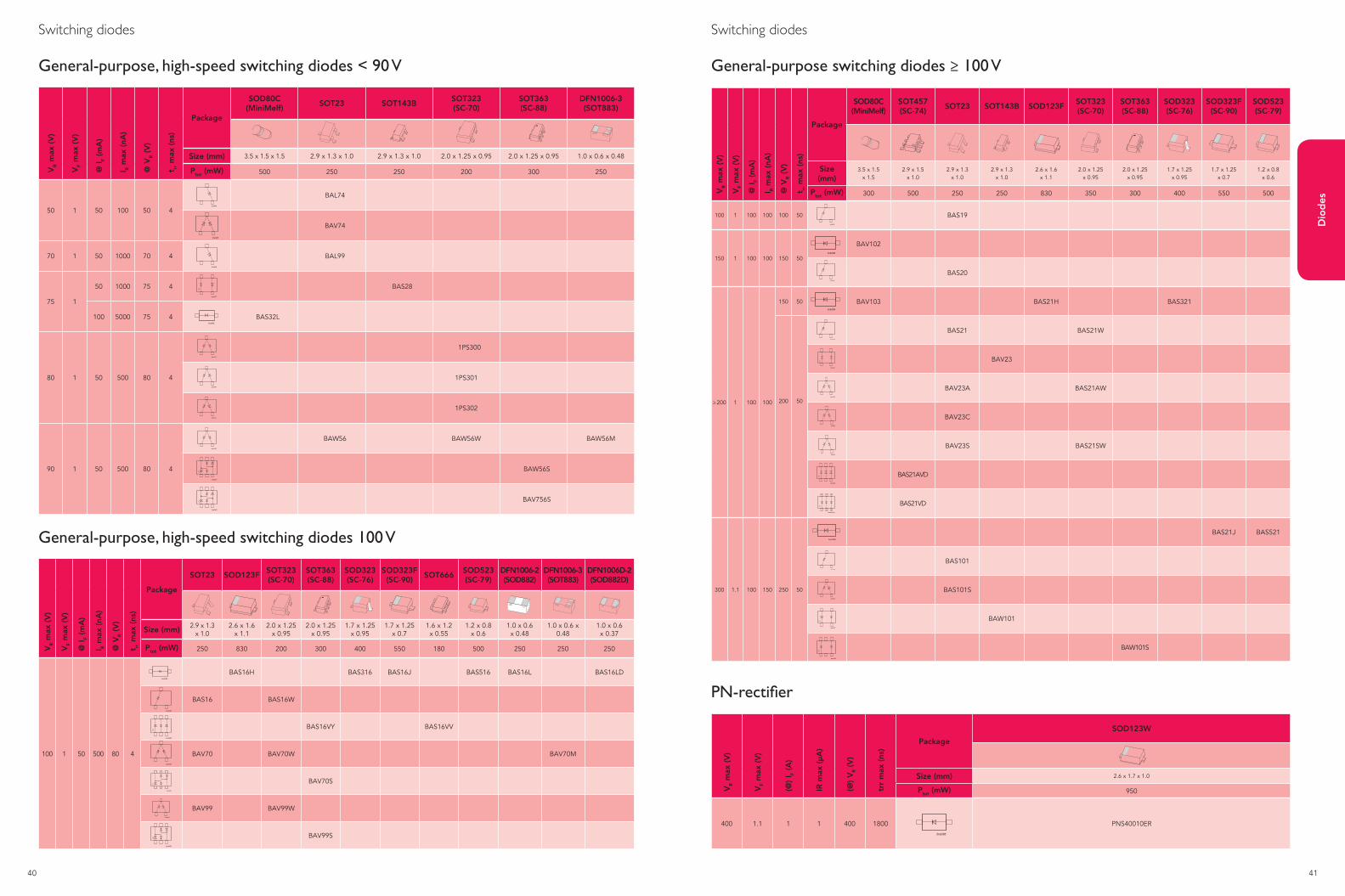
40 41
Dio
des
Switching diodes Switching diodes
General-purpose, high-speed switching diodes < 90 V V
R m
ax (
V)
VF
max
(V
)
@ I
F (m
A)
I R m
ax (
nA)
@ V
R (
V)
t rr m
ax (
ns)
Package
SOD80C (MiniMelf)
SOT23 SOT143BSOT323(SC-70)
SOT363(SC-88)
DFN1006-3 (SOT883)
Size (mm) 3.5 x 1.5 x 1.5 2.9 x 1.3 x 1.0 2.9 x 1.3 x 1.0 2.0 x 1.25 x 0.95 2.0 x 1.25 x 0.95 1.0 x 0.6 x 0.48
Ptot (mW) 500 250 250 200 300 250
50 1 50 100 50 4
BAL74
BAV74
70 1 50 1000 70 4 BAL99
75 1
50 1000 75 4 BAS28
100 5000 75 4 BAS32L
80 1 50 500 80 4
1PS300
1PS301
1PS302
90 1 50 500 80 4
BAW56 BAW56W BAW56M
BAW56S
BAV756S
bra046
bra036
bra037
bra143
bra143
bra046
bra041
M3D088
General-purpose, high-speed switching diodes 100 V
VR m
ax (
V)
VF
max
(V
)
@ I
F (m
A)
I R m
ax (
nA)
@ V
R (
V)
t rr m
ax (
ns)
Package
SOT23 SOD123FSOT323(SC-70)
SOT363(SC-88)
SOD323(SC-76)
SOD323F(SC-90)
SOT666SOD523(SC-79)
DFN1006-2 (SOD882)
DFN1006-3 (SOT883)
DFN1006D-2 (SOD882D)
Size (mm) 2.9 x 1.3 x 1.0
2.6 x 1.6 x 1.1
2.0 x 1.25 x 0.95
2.0 x 1.25 x 0.95
1.7 x 1.25 x 0.95
1.7 x 1.25 x 0.7
1.6 x 1.2 x 0.55
1.2 x 0.8 x 0.6
1.0 x 0.6 x 0.48
1.0 x 0.6 x 0.48
1.0 x 0.6 x 0.37
Ptot (mW) 250 830 200 300 400 550 180 500 250 250 250
100 1 50 500 80 4
BAS16H BAS316 BAS16J BAS516 BAS16L BAS16LD
BAS16 BAS16W
BAS16VY BAS16VV
BAV70 BAV70W BAV70M
BAV70S
BAV99 BAV99W
BAV99S
bra046
bra036
bra048
bra038
bra041
M3D088
General-purpose switching diodes ≥ 100 V
VR m
ax (
V)
VF
max
(V
)
@ I
F (m
A)
I R m
ax (
nA)
@ V
R (
V)
t rr m
ax (
ns)
Package
SOD80C(MiniMelf)
SOT457(SC-74)
SOT23 SOT143B SOD123FSOT323(SC-70)
SOT363(SC-88)
SOD323(SC-76)
SOD323F(SC-90)
SOD523(SC-79)
Size (mm)
3.5 x 1.5x 1.5
2.9 x 1.5x 1.0
2.9 x 1.3x 1.0
2.9 x 1.3x 1.0
2.6 x 1.6x 1.1
2.0 x 1.25x 0.95
2.0 x 1.25x 0.95
1.7 x 1.25x 0.95
1.7 x 1.25x 0.7
1.2 x 0.8x 0.6
Ptot (mW) 300 500 250 250 830 350 300 400 550 500
100 1 100 100 100 50 BAS19
150 1 100 100 150 50
BAV102
BAS20
≥ 200 1 100 100
150 50 BAV103 BAS21H BAS321
200 50
BAS21 BAS21W
BAV23
BAV23A BAS21AW
BAV23C
BAV23S BAS21SW
BAS21AVD
BAS21VD
300 1.1 100 150 250 50
BAS21J BAS521
BAS101
BAS101S
BAW101
BAW101S
bra036
bra036
bra048
bra048
bra048
bra037
bra143
bra046
bra041
bra038
bra036
bra048
bra041
bra037
M3D088
PN-rectifier
VR m
ax (
V)
VF
max
(V
)
(@)
I F (A
)
IR m
ax (
μA)
(@)
VR (
V)
trr
max
(ns
)
Package
SOD123W
Size (mm) 2.6 x 1.7 x 1.0
Ptot (mW) 950
400 1.1 1 1 400 1800 PNS40010ERbra036
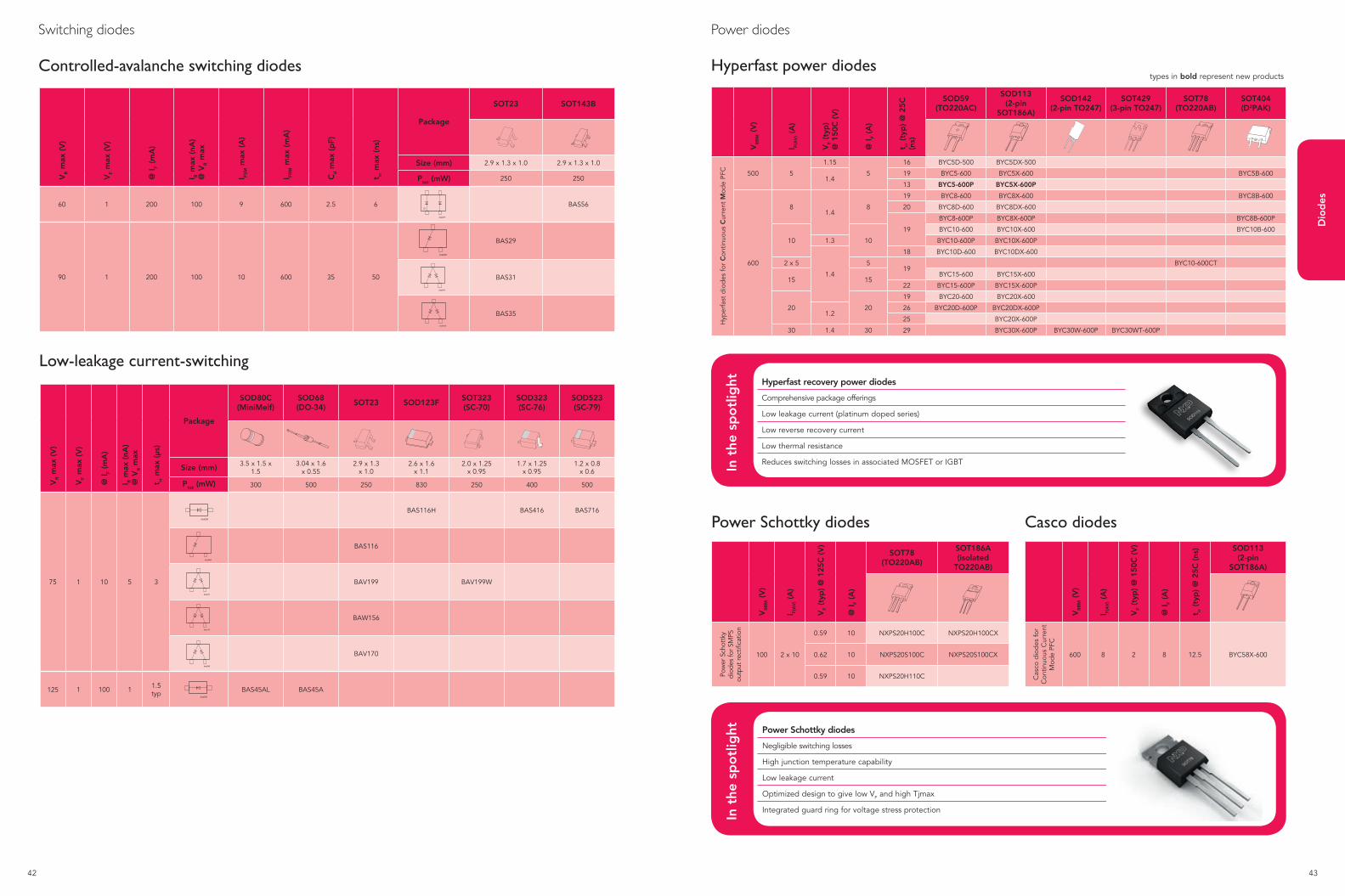
42 43
Dio
des
Switching diodes
Controlled-avalanche switching diodesV
R m
ax (
V)
VF
max
(V
)
@ I
F (m
A)
I R m
ax (
nA)
@ V
R m
ax
I FSM m
ax (
A)
I FRM m
ax (
mA
)
Cd m
ax (
pF)
t rr m
ax (
ns)
Package
SOT23 SOT143B
Size (mm) 2.9 x 1.3 x 1.0 2.9 x 1.3 x 1.0
Ptot (mW) 250 250
60 1 200 100 9 600 2.5 6 BAS56
90 1 200 100 10 600 35 50
BAS29
BAS31
BAS35
M3D088
bra037
bra048
bra041
bra143
VR m
ax (
V)
VF
max
(V
)
@ I
F (m
A)
I R m
ax (
nA)
@ V
R m
ax
t rr m
ax (
μs)
Package
SOD80C(MiniMelf)
SOD68 (DO-34)
SOT23 SOD123FSOT323(SC-70)
SOD323(SC-76)
SOD523(SC-79)
Size (mm) 3.5 x 1.5 x 1.5
3.04 x 1.6 x 0.55
2.9 x 1.3x 1.0
2.6 x 1.6x 1.1
2.0 x 1.25x 0.95
1.7 x 1.25x 0.95
1.2 x 0.8x 0.6
Ptot (mW) 300 500 250 830 250 400 500
75 1 10 5 3
BAS116H BAS416 BAS716
BAS116
BAV199 BAV199W
BAW156
BAV170
125 1 100 1 1.5 typ BAS45AL BAS45A
Low-leakage current-switching
bra036
bra048
bra041
bra143
bra046
bra036
M3D088
M3D
050
VR
RM (
V)
I F(A
V) (
A)
VF
(typ
)
@ 1
50C
(V
)
@ I
F (A
)
t rr (
typ
) @
25C
(n
s)
SOD59 (TO220AC)
SOD113 (2-pin
SOT186A)
SOD142(2-pin TO247)
SOT429(3-pin TO247)
SOT78(TO220AB)
SOT404(D2PAK)
Hyp
erfa
st d
iod
es fo
r C
ontin
uous
Cur
rent
Mod
e PF
C 500 5
1.15
5
16 BYC5D-500 BYC5DX-500
1.419 BYC5-600 BYC5X-600 BYC5B-600
13 BYC5-600P BYC5X-600P
600
81.4
8
19 BYC8-600 BYC8X-600 BYC8B-600
20 BYC8D-600 BYC8DX-600
19
BYC8-600P BYC8X-600P BYC8B-600P
10 10
BYC10-600 BYC10X-600 BYC10B-600
1.3 BYC10-600P BYC10X-600P
1.4
18 BYC10D-600 BYC10DX-600
2 x 5 519
BYC10-600CT
15 15BYC15-600 BYC15X-600
22 BYC15-600P BYC15X-600P
20 20
19 BYC20-600 BYC20X-600
1.226 BYC20D-600P BYC20DX-600P
25 BYC20X-600P
30 1.4 30 29 BYC30X-600P BYC30W-600P BYC30WT-600P
Power diodes
Hyperfast power diodestypes in bold represent new products
In t
he S
po
tlig
ht Hyperfast recovery power diodes
Comprehensive package offerings
Low leakage current (platinum doped series)
Low reverse recovery current
Low thermal resistance
Reduces switching losses in associated MOSFET or IGBTIn t
he s
po
tlig
ht
Power Schottky diodes Casco diodes
VR
RM (
V)
I F(A
V) (
A)
VF
(typ
) @
125
C (
V)
@ I
F (A
)
SOT78 (TO220AB)
SOT186A (isolated
TO220AB)
Pow
er S
chot
tky
diod
es fo
r SM
PS
outp
ut re
ctifi
catio
n
100 2 x 10
0.59 10 NXPS20H100C NXPS20H100CX
0.62 10 NXPS20S100C NXPS20S100CX
0.59 10 NXPS20H110C
VR
RM (
V)
I F(A
V) (
A)
VF
(typ
) @
150
C (
V)
@ I
F (A
)
t rr (
typ
) @
25C
(ns
) SOD113(2-pin
SOT186A)
Cas
co d
iod
es fo
r C
ontin
uous
Cur
rent
M
ode
PFC
600 8 2 8 12.5 BYC58X-600
In t
he S
po
tlig
ht Power Schottky diodes
Negligible switching losses
High junction temperature capability
Low leakage current
Optimized design to give low VF and high Tjmax
Integrated guard ring for voltage stress protectionIn t
he s
po
tlig
ht
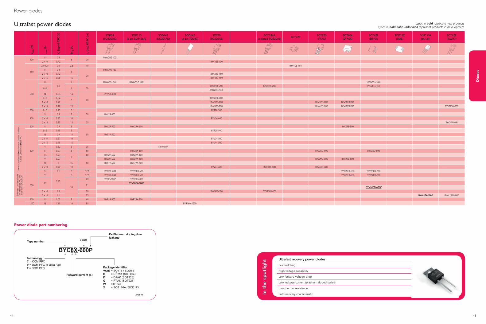
44 45
Dio
des
In t
he S
po
tlig
htUltrafast recovery power diodes
Fast switching
High voltage capability
Low forward voltage drop
Low leakage current (platinum doped series)
Low thermal resistance
Soft recovery characteristicIn t
he s
po
tlig
ht
Power diode part numbering
brb644
Type number
Forward current (IF)
BYC8X-600P
VRRM
Package identifierVOIDBDGWX
= SOT78 / SOD59= D2PAK (SOT404)= DPAK (SOT428)= I2PAK (SOT226)=TO247= SOT186A / SOD113
Technology:C = CCM PFCV = DCM PFC or Ultra FastT = DCM PFC
P= Platinum doping /low leakage
Power diodes
VRR
M (V
)
I F(A
V) (
A)
VF (
typ)
@ 1
50C
(V)
@ I F (
A)
t rr (t
yp) @
25C
(ns) SOD59
(TO220AC)SOD113
(2-pin SOT186A)SOD141
(DO201AD)SOD142
(2-pin TO247)SOT78
(TO220AB)SOT186A
(isolated TO220AB)SOT223
SOT226 (I2PAK)
SOT404 (D2PAK)
SOT428(DPAK)
SOD132(SMB)
SOT1259(TO-3P)
SOT429(TO247)
1008 0.8
8 20BYW29E-100
2 x 10 0.72 BYV32E-100
150
2 x 0.75 0.5 0.5 10 BYV40E-150
8 0.88
20
BYW29E-150
2 x 10 0.72 BYV32E-150
2 x 15 0.78 15 BYV42E-150
200
8
0.8
8 BYW29E-200 BYW29EX-200 BYW29ED-200
2 x 5 5 15BYQ28E-200 BYQ28X-200 BYQ28ED-200
BYQ28E-200E
14 0.83 14
20
BYV79E-200
2 x 8 0.848
BYQ30E-200
2 x 10 0.72 BYV32E-200 BYV32G-200 BYV32EB-200
2 x 15 0.78 15 BYV42E-200 BYV42G-200 BYV42EB-200 BYV72EW-200
300 2 x 5 0.95 5
50
BYT28-300
400
9 0.9 8 BYV29-400
2 x 10 0.87 10 BYV34-400
2 x 15 0.95 15 35 BYV74W-400
Ultra
fast
dio
des f
or D
iscon
tinuo
us C
urre
nt M
ode
or
Criti
cal C
ondu
ctio
n M
ode
PFC
500 9 0.9 8
50
BYV29-500 BYV29X-500 BYV29B-500
600
2 x 5 0.95 5 BYT28-500
15 0.9 15 BYT79-500
2 x 10 0.87 10 BYV34-500
2 x 15 0.95 15 BYV44-500
4 0.82 3 35 NUR460P
5 0.97 5 50 BYV25X-600 BYV25G-600 BYV25D-600
8 1.078
60 BYR29-600 BYR29X-600
9 0.97
50
BYV29-600 BYV29X-600 BYV29G-600 BYV29B-600
15 1 15 BYT79-600 BYT79X-600
2 x 10 0.92 10 BYV34-600 BYV34X-600 BYV34G-600
5 1.1 5 17.5 BYV25F-600 BYV25FX-600 BYV25FB-600 BYV25FD-600
Enha
nced
ultr
afas
t dio
des
for i
nter
leav
ed P
FC a
nd
dual
-mod
e D
CM/C
CM
600
9
1.25
8 17.5 BYV29F-600 BYV29FX-600 BYV29FB-600 BYV29FD-600
10
10
20 BYV10-600P BYV10X-600P
21BYV10EX-600P
BYV10ED-600P
2 x 10 1.3 20 BYV410-600 BYV410X-600
2 x 15 1.1 25 BYV415K-600P BYV415W-600P
800 8 1.07 8 60 BYR29-800 BYR29X-800
1200 16 1.65 16 80 BYR16W-1200
Ultrafast power diodes types in bold represent new productsTypes in bold italic underlined represent products in development
46 47
ESD protection, filtering and signal conditioning
Ultra low-capacitance ESD protection devices 53
Low-capacitance ESD protection devices 57
Standard ESD protection devices 61
Application-specific ESD and ESD/EMI solutions 63USB 2.0 protection and filtering 63Common Mode Filter for USB 2.0 63USB 3.x and eSATA protection and filtering 64Common Mode Filter for USB 3.x 65Common Mode Filter for video interfaces 66Ethernet protection 66HDMI and memory-card signal conditioning 67Video interface protection 68NFC antenna protection 69LCD and camera protection and filtering 70Audio interface protection and filtering 71Memory- and SIM-card protection and filtering 71Battery and charger protection 71Automotive high-speed network protection 72Automotive in-vehicle network bus line protection 72
Transient voltage suppressor (TVS) diodes 74TVS diodes, 24 / 40 W 74TVS diodes for mobile applications 74TVS diodes, 400 W 75TVS diodes, 600 W 76
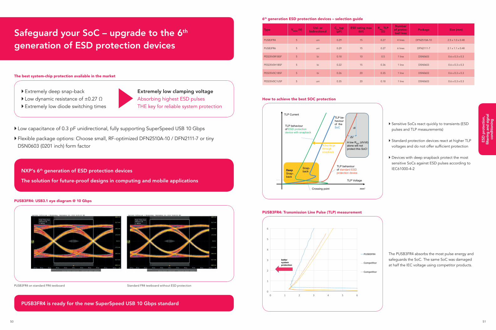
50 51
ESD
pro
tect
ion,
fil
terin
g a
nd s
igna
l co
nditi
onin
g
Safeguard your SoC – upgrade to the 6th generation of ESD protection devices
PUSB3FR4: USB3.1 eye diagram @ 10 Gbps
The best system-chip protection available in the market
6th generation ESD protection devices – selection guide
How to achieve the best SOC protection
PUSB3FR4: Transmission Line Pulse (TLP) measurement
0
1
2
3
4
5
6
0 1 2 3 4 5 6
PUSB3FR4
Competitor 1
Competitor 2
better system protection
Low capacitance of 0.3 pF unidirectional, fully supporting SuperSpeed USB 10 Gbps
Flexible package options: Choose small, RF-optimized DFN2510A-10 / DFN2111-7 or tiny DSN0603 (0201 inch) form factor
PUSB3FR4 on standard FR4 testboard Standard FR4 testboard without ESD protection
Sensitive SoCs react quickly to transients (ESD pulses and TLP measurements)
Standard protection devices react at higher TLP voltages and do not offer sufficient protection
Devices with deep snapback protect the most sensitive SoCs against ESD pulses according to IEC61000-4-2
The PUSB3FR4 absorbs the most pulse energy and safeguards the SoC. The same SoC was damaged at half the IEC voltage using competitor products.
Extremely deep snap-back Low dynamic resistance of ±0.27 Ω Extremely low diode switching times
Extremely low clamping voltage
Absorbing highest ESD pulsesTHE key for reliable system protection
NXP‘s 6th generation of ESD protection devices
The solution for future-proof designs in computing and mobile applications
PUSB3FR4 is ready for the new SuperSpeed USB 10 Gbps standard
Type VRWM (V)Uni- or
bidirectionalClinetyp
(pF)ESD rating max
(kV)Rdyn TLP
(Ω)
Number of protec-ted lines
Package Size (mm)
PUSB3FR4 5 uni 0.29 15 0.27 4 lines DFN2510A-10 2.5 x 1.0 x 0.48
PUSB3FR6 5 uni 0.29 15 0.27 6 lines DFN2111-7 2.1 x 1.1 x 0.48
PESD5V0R1BSF 5 bi 0.18 10 0.5 1 line DSN0603 0.6 x 0.3 x 0.3
PESD5V0H1BSF 5 bi 0.22 15 0.36 1 line DSN0603 0.6 x 0.3 x 0.3
PESD5V0C1BSF 5 bi 0.26 20 0.35 1 line DSN0603 0.6 x 0.3 x 0.3
PESD5V0C1USF 5 uni 0.35 20 0.18 1 line DSN0603 0.6 x 0.3 x 0.3
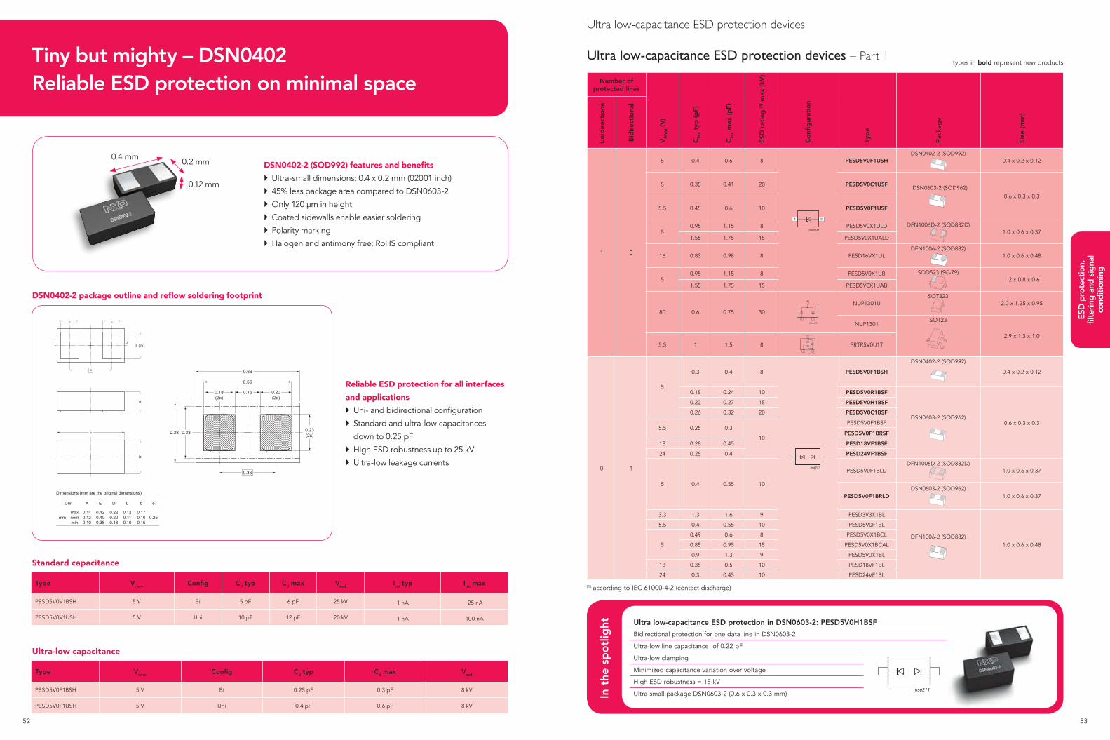
52 53
ESD
pro
tect
ion,
fil
terin
g a
nd s
igna
l co
nditi
onin
g
Tiny but mighty – DSN0402 Reliable ESD protection on minimal space
Standard capacitance
Type Vrwm Config Cd typ Cd max Vesd Irm typ Irm max
PESD5V0V1BSH 5 V Bi 5 pF 6 pF 25 kV 1 nA 25 nA
PESD5V0V1USH 5 V Uni 10 pF 12 pF 20 kV 1 nA 100 nA
Ultra-low capacitance
Type Vrwm Config Cd typ Cd max Vesd
PESD5V0F1BSH 5 V Bi 0.25 pF 0.3 pF 8 kV
PESD5V0F1USH 5 V Uni 0.4 pF 0.6 pF 8 kV
Reliable ESD protection for all interfaces
and applications
Uni- and bidirectional configuration
Standard and ultra-low capacitances
down to 0.25 pF
High ESD robustness up to 25 kV
Ultra-low leakage currents
DSN0402-2 (SOD992) features and benefits
Ultra-small dimensions: 0.4 x 0.2 mm (02001 inch)
45% less package area compared to DSN0603-2
Only 120 µm in height
Coated sidewalls enable easier soldering
Polarity marking
Halogen and antimony free; RoHS compliant
Ultra low-capacitance ESD protection devices
Ultra low-capacitance ESD protection in DSN0603-2: PESD5V0H1BSF
Bidirectional protection for one data line in DSN0603-2
Ultra-low line capacitance of 0.22 pF
Ultra-low clamping
Minimized capacitance variation over voltage
High ESD robustness = 15 kV
Ultra-small package DSN0603-2 (0.6 x 0.3 x 0.3 mm)In t
he s
po
tlig
ht
mse211
Ultra low-capacitance ESD protection devices – Part 1
Number of protected lines
VR
WM (
V)
Clin
e ty
p (
pF)
Clin
e m
ax (
pF)
ESD
rat
ing
[1] m
ax (
kV)
Co
nfig
urat
ion
Typ
e
Pac
kag
e
Size
(m
m)
Uni
dir
ecti
ona
l
Bid
irec
tio
nal
1 0
5 0.4 0.6 8 PESD5V0F1USHDSN0402-2 (SOD992)
0.4 x 0.2 x 0.12
5 0.35 0.41 20 PESD5V0C1USF DSN0603-2 (SOD962)
0.6 x 0.3 x 0.3
5.5 0.45 0.6 10 PESD5V0F1USF
50.95 1.15 8 PESD5V0X1ULD DFN1006D-2 (SOD882D)
1.0 x 0.6 x 0.371.55 1.75 15 PESD5V0X1UALD
16 0.83 0.98 8 PESD16VX1ULDFN1006-2 (SOD882)
1.0 x 0.6 x 0.48
50.95 1.15 8 PESD5V0X1UB SOD523 (SC-79)
1.2 x 0.8 x 0.61.55 1.75 15 PESD5V0X1UAB
80 0.6 0.75 30
NUP1301USOT323
2.0 x 1.25 x 0.95
NUP1301SOT23
2.9 x 1.3 x 1.0
5.5 1 1.5 8 PRTR5V0U1T
0 1
5
0.3 0.4 8 PESD5V0F1BSH
DSN0402-2 (SOD992)
0.4 x 0.2 x 0.12
0.18 0.24 10 PESD5V0R1BSF
DSN0603-2 (SOD962)0.6 x 0.3 x 0.3
0.22 0.27 15 PESD5V0H1BSF
0.26 0.32 20 PESD5V0C1BSF
5.5 0.25 0.3
10
PESD5V0F1BSF
PESD5V0F1BRSF
18 0.28 0.45 PESD18VF1BSF
24 0.25 0.4 PESD24VF1BSF
5 0.4 0.55 10
PESD5V0F1BLDDFN1006D-2 (SOD882D)
1.0 x 0.6 x 0.37
PESD5V0F1BRLDDSN0603-2 (SOD962)
1.0 x 0.6 x 0.37
3.3 1.3 1.6 9 PESD3V3X1BL
DFN1006-2 (SOD882)1.0 x 0.6 x 0.48
5.5 0.4 0.55 10 PESD5V0F1BL
5
0.49 0.6 8 PESD5V0X1BCL
0.85 0.95 15 PESD5V0X1BCAL
0.9 1.3 9 PESD5V0X1BL
18 0.35 0.5 10 PESD18VF1BL
24 0.3 0.45 10 PESD24VF1BL
types in bold represent new products
mse209
1 2
21006aab111
3
mse211
006aaa763
1 2
3
[1] according to IEC 61000-4-2 (contact discharge)
DSN0402-2 package outline and reflow soldering footprint
ReferencesOutlineversion
Europeanprojection Issue date
IEC JEDEC JEITA
SOD992
sod992_po
13-10-2813-11-01
Unit
mmmaxnommin
0.14 0.42 0.12 0.170.250.40
0.38
A
Dimensions (mm are the original dimensions)
E D
0.22
0.10 0.150.18
L b e
0 0.5 mm
scale
A
E
D
LL
b (2x)1 2
e
0.12 0.20 0.11 0.160.10
ReferencesOutlineversion
Europeanprojection Issue date
IEC JEDEC JEITA
SOD992
sod992_po
13-10-2813-11-01
Unit
mmmaxnommin
0.14 0.42 0.12 0.170.250.40
0.38
A
Dimensions (mm are the original dimensions)
E D
0.22
0.10 0.150.18
L b e
0 0.5 mm
scale
A
E
D
LL
b (2x)1 2
e
0.12 0.20 0.11 0.160.10
occupied area
solder paste
solder resist
solder lands
Dimensions in mm14-08-2214-08-25
0.23(2x)
0.18(2x)
0.20(2x)
0.16
0.66
0.56
0.36
0.330.38
0.4 mm 0.2 mm
0.12 mm
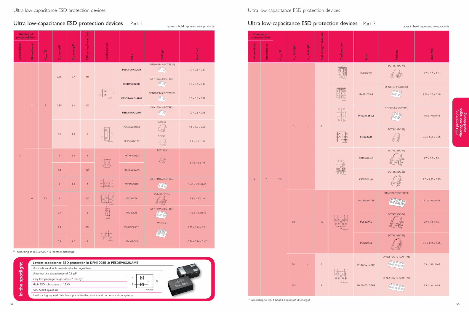
54 55
ESD
pro
tect
ion,
fil
terin
g a
nd s
igna
l co
nditi
onin
g
Ultra low-capacitance ESD protection devices
[1] according to IEC 61000-4-5 (contact discharge)
Ultra low-capacitance ESD protection devices – Part 2
Number of protected lines
VR
WM (
V)
Clin
e ty
p (
pF)
Clin
e m
ax (
pF)
ESD
rat
ing
[1] m
ax (
kV)
Co
nfig
urat
ion
Typ
e
Pac
kag
e
Size
(m
m)
Uni
dir
ecti
ona
l
Bid
irec
tio
nal
2
1 5
0.55 0.7 10
PESD5V0X2UMB
DFN1006B-3 (SOT883B)
1.0 x 0.6 x 0.37
PESD5V0X2UM
DFN1006-3 (SOT883)
1.0 x 0.6 x 0.48
0.85 1.1 15
PESD5V0X2UAMB
DFN1006B-3 (SOT883B)
1.0 x 0.6 x 0.37
PESD5V0X2UAM
DFN1006-3 (SOT883)
1.0 x 0.6 x 0.48
0.9 1.3 9
PESD5V0X1BQ
SOT663
1.6 x 1.2 x 0.55
PESD5V0X1BT
SOT23
2.9 x 1.3 x 1.0
0 5.5
1 1.5 8 PRTR5V0U2X
SOT143B
2.9 x 1.3 x 1.0
1.8 - 12 PRTR5V0U2AX
1 1.5 8 PRTR5V0U2F
DFN1410-6 (SOT886)
1.45 x 1.0 x 0.48
2
-
15 IP4234CZ6
SOT457 (SC-74)
2.9 x 1.5 x 1.0
0.7 8 IP4282CZ6
DFN1410-6 (SOT886)
1.45 x 1.0 x 0.48
1.3 15 IP4359CX4/LF
WLCSP4
0.76 x 0.76 x 0.61
0.8 1.0 8 IP4369CX4 0.76 x 0.76 x 0.47
types in bold represent new products
3
R R
65
2 001aaj950
1 4
2
3, 4001aaj776
1
008aaa239
A1 A2
B1 B2
brb182
1
3
5
6
2
I/O1
I/O2
GND
4
VBUS
I/O1
I/O2
1
2
001aaa490
3
brb051
1
23
Lowest capacitance ESD protection in DFN1006B-3: PESD5V0X2UAMB
Unidirectional double protection for two signal lines
Ultra-low line capacitance of 0.8 pF
Very low package height of 0.37 mm typ
High ESD robustness of 15 kV
AEC-Q101 qualified
Ideal for high-speed data lines, portable electronics, and communication systemsIn t
he s
po
tlig
ht
brb051
1
23
Ultra low-capacitance ESD protection devices
Number of protected lines
VR
WM (
V)
Clin
e ty
p (
pF)
Clin
e m
ax (
pF)
ESD
rat
ing
[1] m
ax (
kV)
Co
nfig
urat
ion
Typ
e
Pac
kag
e
Size
(m
m)
Uni
dir
ecti
ona
l
Bid
irec
tio
nal
4 0 5.5
1 - 8
IP4220CZ6
SOT457 (SC-74)
2.9 x 1.5 x 1.0
IP4221CZ6-S
DFN1410-6 (SOT886)
1.45 x 1.0 x 0.48
IP4221CZ6-XS
DFN1010-6 (SOT891)
1.0 x 1.0 x 0.48
IP4233CZ6
SOT363 (SC-88)
2.0 x 1.25 x 0.95
PRTR5V0U4D
SOT457 (SC-74)
2.9 x 1.5 x 1.0
PRTR5V0U4Y
SOT363 (SC-88)
2.0 x 1.25 x 0.95
0.8 - 12
IP4285CZ9-TBB
DFN2110-9 (SOT1178)
2.1 x 1.0 x 0.48
PUSB2X4D
SOT457 (SC-74)
2.9 x 1.5 x 1.0
PUSB2X4Y
SOT363 (SC-88)
2.0 x 1.25 x 0.95
0.6 - 8 IP4283CZ10-TBR
DFN2510A-10 (SOT1176)
2.5 x 1.0 x 0.48
0.5 - 8 IP4284CZ10-TBR
DFN2510A-10 (SOT1176)
2.5 x 1.0 x 0.48
[1] according to IEC 61000-4-5 (contact discharge)
types in bold represent new productsUltra low-capacitance ESD protection devices – Part 3
2 4
3, 8 001aai619
1 5
001aag273
1 2 3
6 5 4
2 4
3, 8 001aai619
1 5
001aac379
1 2 3
6 5 4
001aag273
1 2 3
6 5 4
001aaj811
1
2
3
6
5
4
001aag273
1 2 3
6 5 4
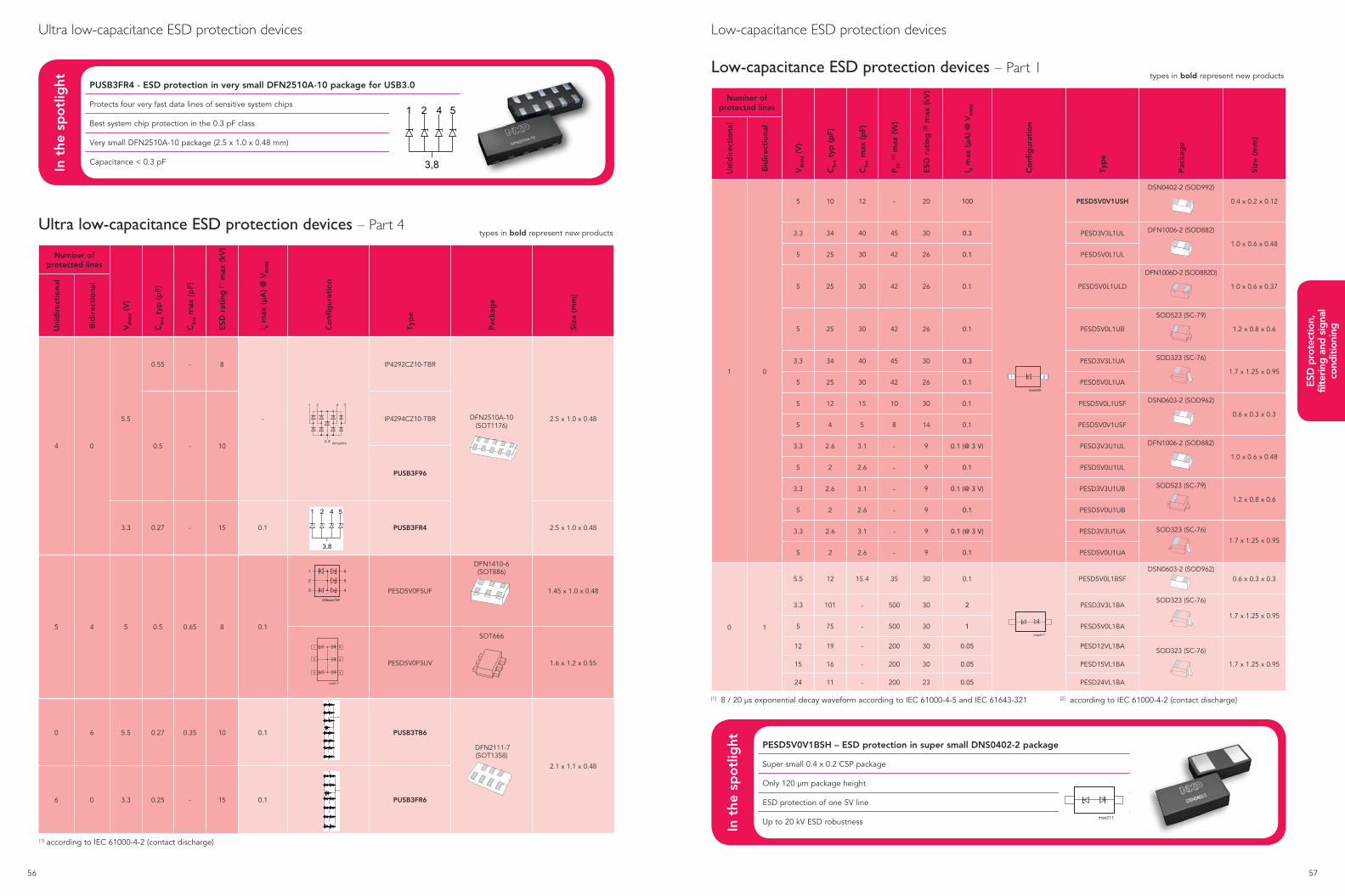
56 57
ESD
pro
tect
ion,
fil
terin
g a
nd s
igna
l co
nditi
onin
g
Ultra low-capacitance ESD protection devices – Part 4
Number of protected lines
VR
WM (
V)
Clin
e ty
p (
pF)
Clin
e m
ax (
pF)
ESD
rat
ing
[1] m
ax (
kV)
I R m
ax (
µA)
@ V
RW
M
Co
nfig
urat
ion
Typ
e
Pac
kag
e
Size
(m
m)
Uni
dir
ecti
ona
l
Bid
irec
tio
nal
4 0
5.5
0.55 - 8
-
IP4292CZ10-TBR
DFN2510A-10 (SOT1176)
2.5 x 1.0 x 0.48
0.5 - 10
IP4294CZ10-TBR
PUSB3F96
3.3 0.27 - 15 0.1 PUSB3FR4 2.5 x 1.0 x 0.48
5 4 5 0.5 0.65 8 0.1
PESD5V0F5UF
DFN1410-6 (SOT886)
1.45 x 1.0 x 0.48
PESD5V0F5UV
SOT666
1.6 x 1.2 x 0.55
0 6 5.5 0.27 0.35 10 0.1 PUSB3TB6
DFN2111-7(SOT1358)
2.1 x 1.1 x 0.48
6 0 3.3 0.25 - 15 0.1 PUSB3FR6
[1] according to IEC 61000-4-2 (contact discharge)
types in bold represent new products
2 4
3, 8 001aai619
1 5
61
52
43
006aaa159
Ultra low-capacitance ESD protection devices
In t
he s
po
tlig
ht PUSB3FR4 - ESD protection in very small DFN2510A-10 package for USB3.0
Protects four very fast data lines of sensitive system chips
Best system chip protection in the 0.3 pF class
Very small DFN2510A-10 package (2.5 x 1.0 x 0.48 mm)
Capacitance < 0.3 pF
3,8
1 2 4 5
3,8
1 2 4 5
In t
he s
po
tlig
ht PESD5V0V1BSH – ESD protection in super small DNS0402-2 package
Super small 0.4 x 0.2 CSP package
Only 120 µm package height
ESD protection of one 5V line
Up to 20 kV ESD robustness
Low-capacitance ESD protection devices
Number of protected lines
VR
WM (
V)
Clin
e ty
p (
pF)
Clin
e m
ax (
pF)
PP
P [1
] max
(W
)
ESD
rat
ing
[2] m
ax (
kV)
I R m
ax (
µA)
@ V
RW
M
Co
nfig
urat
ion
Typ
e
Pac
kag
e
Size
(m
m)
Uni
dir
ecti
ona
l
Bid
irec
tio
nal
1 0
5 10 12 - 20 100 PESD5V0V1USH
DSN0402-2 (SOD992)
0.4 x 0.2 x 0.12
3.3 34 40 45 30 0.3 PESD3V3L1UL DFN1006-2 (SOD882)
1.0 x 0.6 x 0.48
5 25 30 42 26 0.1 PESD5V0L1UL
5 25 30 42 26 0.1 PESD5V0L1ULD
DFN1006D-2 (SOD882D)
1.0 x 0.6 x 0.37
5 25 30 42 26 0.1 PESD5V0L1UB
SOD523 (SC-79)
1.2 x 0.8 x 0.6
3.3 34 40 45 30 0.3 PESD3V3L1UA SOD323 (SC-76)
1.7 x 1.25 x 0.95
5 25 30 42 26 0.1 PESD5V0L1UA
5 12 15 10 30 0.1 PESD5V0L1USF DSN0603-2 (SOD962)
0.6 x 0.3 x 0.3
5 4 5 8 14 0.1 PESD5V0V1USF
3.3 2.6 3.1 - 9 0.1 (@ 3 V) PESD3V3U1UL DFN1006-2 (SOD882)
1.0 x 0.6 x 0.48
5 2 2.6 - 9 0.1 PESD5V0U1UL
3.3 2.6 3.1 - 9 0.1 (@ 3 V) PESD3V3U1UB SOD523 (SC-79)
1.2 x 0.8 x 0.6
5 2 2.6 - 9 0.1 PESD5V0U1UB
3.3 2.6 3.1 - 9 0.1 (@ 3 V) PESD3V3U1UA SOD323 (SC-76)
1.7 x 1.25 x 0.95
5 2 2.6 - 9 0.1 PESD5V0U1UA
0 1
5.5 12 15.4 35 30 0.1 PESD5V0L1BSFDSN0603-2 (SOD962)
0.6 x 0.3 x 0.3
3.3 101 - 500 30 2 PESD3V3L1BASOD323 (SC-76)
1.7 x 1.25 x 0.95
5 75 - 500 30 1 PESD5V0L1BA
12 19 - 200 30 0.05 PESD12VL1BASOD323 (SC-76)
1.7 x 1.25 x 0.9515 16 - 200 30 0.05 PESD15VL1BA
24 11 - 200 23 0.05 PESD24VL1BA
Low-capacitance ESD protection devices – Part 1
[1] 8 / 20 µs exponential decay waveform according to IEC 61000-4-5 and IEC 61643-321 [2] according to IEC 61000-4-2 (contact discharge)
types in bold represent new products
mse209
1 2
mse211
mse211
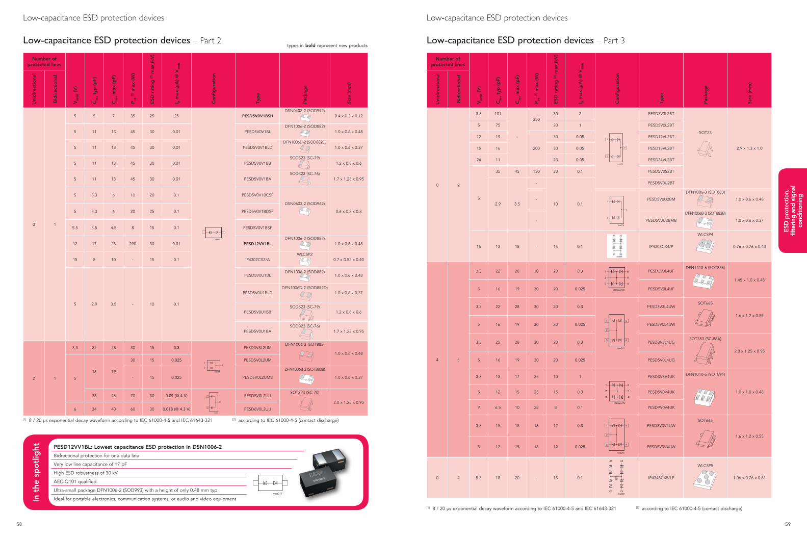
58 59
ESD
pro
tect
ion,
fil
terin
g a
nd s
igna
l co
nditi
onin
g
Low-capacitance ESD protection devices – Part 2
Low-capacitance ESD protection devices
Number of protected lines
VR
WM (
V)
Clin
e ty
p (
pF)
Clin
e m
ax (
pF)
PP
P [1
] max
(W
)
ESD
rat
ing
[2] m
ax (
kV)
I R m
ax (
µA)
@ V
RW
M
Co
nfig
urat
ion
Typ
e
Pac
kag
e
Size
(m
m)
Uni
dir
ecti
ona
l
Bid
irec
tio
nal
0 1
5 5 7 35 25 25 PESD5V0V1BSHDSN0402-2 (SOD992)
0.4 x 0.2 x 0.12
5 11 13 45 30 0.01 PESD5V0V1BLDFN1006-2 (SOD882)
1.0 x 0.6 x 0.48
5 11 13 45 30 0.01 PESD5V0V1BLDDFN1006D-2 (SOD882D)
1.0 x 0.6 x 0.37
5 11 13 45 30 0.01 PESD5V0V1BBSOD523 (SC-79)
1.2 x 0.8 x 0.6
5 11 13 45 30 0.01 PESD5V0V1BASOD323 (SC-76)
1.7 x 1.25 x 0.95
5 5.3 6 10 20 0.1 PESD5V0V1BCSF
DSN0603-2 (SOD962)
0.6 x 0.3 x 0.35 5.3 6 20 25 0.1 PESD5V0V1BDSF
5.5 3.5 4.5 8 15 0.1 PESD5V0V1BSF
12 17 25 290 30 0.01 PESD12VV1BLDFN1006-2 (SOD882)
1.0 x 0.6 x 0.48
15 8 10 - 15 0.1 IP4302CX2/AWLCSP2
0.7 x 0.52 x 0.40
5 2.9 3.5 - 10 0.1
PESD5V0U1BLDFN1006-2 (SOD882)
1.0 x 0.6 x 0.48
PESD5V0U1BLDDFN1006D-2 (SOD882D)
1.0 x 0.6 x 0.37
PESD5V0U1BBSOD523 (SC-79)
1.2 x 0.8 x 0.6
PESD5V0U1BASOD323 (SC-76)
1.7 x 1.25 x 0.95
2 1
3.3 22 28 30 15 0.3 PESD3V3L2UMDFN1006-3 (SOT883)
1.0 x 0.6 x 0.48
5
16 19
30 15 0.025 PESD5V0L2UM
- 15 0.025 PESD5V0L2UMB
DFN1006B-3 (SOT883B)
1.0 x 0.6 x 0.37
38 46 70 30 0.09 (@ 4 V) PESD5V0L2UUSOT323 (SC-70)
2.0 x 1.25 x 0.95
6 34 40 60 30 0.018 (@ 4.3 V) PESD6V0L2UU
[1] 8 / 20 µs exponential decay waveform according to IEC 61000-4-5 and IEC 61643-321 [2] according to IEC 61000-4-5 (contact discharge)
mse211
brb051
1
23
types in bold represent new products
In t
he s
po
tlig
ht PESD12VV1BL: Lowest capacitance ESD protection in DSN1006-2
Bidrectional protection for one data line
Very low line capacitance of 17 pF
High ESD robustness of 30 kV
AEC-Q101 qualified
Ultra-small package DFN1006-2 (SOD993) with a height of only 0.48 mm typ
Ideal for portable electronics, communication systems, or audio and video equipmentmse211
Number of protected lines
VR
WM (
V)
Clin
e ty
p (
pF)
Clin
e m
ax (
pF)
PP
P [1
] max
(W
)
ESD
rat
ing
[2] m
ax (
kV)
I R m
ax (
µA)
@ V
RW
M
Co
nfig
urat
ion
Typ
e
Pac
kag
e
Size
(m
m)
Uni
dir
ecti
ona
l
Bid
irec
tio
nal
0 2
3.3 101
-
35030 2 PESD3V3L2BT
SOT23
2.9 x 1.3 x 1.0
5 75 30 1 PESD5V0L2BT
12 19
200
30 0.05 PESD12VL2BT
15 16 30 0.05 PESD15VL2BT
24 11 23 0.05 PESD24VL2BT
5
35 45 130 30 0.1 PESD5V0S2BT
2.9 3.5
-
10 0.1
PESD5V0U2BT
- PESD5V0U2BM
DFN1006-3 (SOT883)
1.0 x 0.6 x 0.48
- PESD5V0U2BMB
DFN1006B-3 (SOT883B)
1.0 x 0.6 x 0.37
15 13 15 - 15 0.1 IP4303CX4/P
WLCSP4
0.76 x 0.76 x 0.40
4 3
3.3 22 28 30 20 0.3 PESD3V3L4UFDFN1410-6 (SOT886)
1.45 x 1.0 x 0.48
5 16 19 30 20 0.025 PESD5V0L4UF
3.3 22 28 30 20 0.3 PESD3V3L4UWSOT665
1.6 x 1.2 x 0.55
5 16 19 30 20 0.025 PESD5V0L4UW
3.3 22 28 30 20 0.3 PESD3V3L4UGSOT353 (SC-88A)
2.0 x 1.25 x 0.95
5 16 19 30 20 0.025 PESD5V0L4UG
3.3 13 17 25 10 1 PESD3V3V4UK DFN1010-6 (SOT891)
1.0 x 1.0 x 0.485 12 15 25 15 0.3 PESD5V0V4UK
9 6.5 10 28 8 0.1 PESD9V0V4UK
3.3 15 18 16 12 0.3 PESD3V3V4UWSOT665
1.6 x 1.2 x 0.55
5 12 15 16 12 0.025 PESD5V0V4UW
0 4 5.5 18 20 - 15 0.1 IP4343CX5/LF
WLCSP5
1.06 x 0.76 x 0.61
Low-capacitance ESD protection devices – Part 3
Low-capacitance ESD protection devices
[1] 8 / 20 µs exponential decay waveform according to IEC 61000-4-5 and IEC 61643-321 [2] according to IEC 61000-4-5 (contact discharge)
006aab474
61
2
43
5
006aaa156
61
52
43
bra986
A1
B2
A3
C1 C3
mse213
1
2
3
brb178
1
2
3
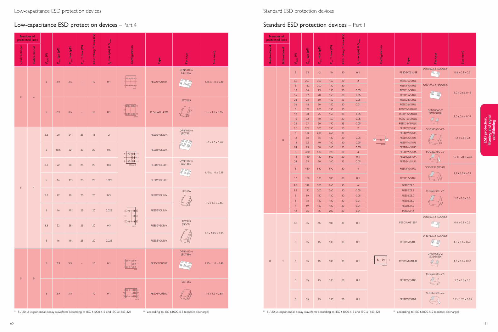
60 61
ESD
pro
tect
ion,
fil
terin
g a
nd s
igna
l co
nditi
onin
g
Number of protected lines
VR
WM (
V)
Clin
e ty
p (
pF)
Clin
e m
ax (
pF)
PP
P [1
] max
(W
)
ESD
rat
ing
[2] m
ax (
kV)
I R m
ax (
µA)
@ V
RW
M
Co
nfig
urat
ion
Typ
e
Pac
kag
e
Size
(m
m)
Uni
dir
ecti
ona
l
Bid
irec
tio
nal
0 4
5 2.9 3.5 - 10 0.1 PESD5V0U4BF
DFN1410-6 (SOT886)
1.45 x 1.0 x 0.48
5 2.9 3.5 - 10 0.1 PESD5V0U4BW
SOT665
1.6 x 1.2 x 0.55
5 4
3.3 20 24 28 15 2 PESD3V3L5UK
DFN1010-6 (SOT891)
1.0 x 1.0 x 0.48
5 18.5 22 30 20 0.5 PESD5V0L5UK
3.3 22 28 25 20 0.3 PESD3V3L5UF
DFN1410-6 (SOT886)
1.45 x 1.0 x 0.48
5 16 19 25 20 0.025 PESD5V0L5UF
3.3 22 28 25 20 0.3 PESD3V3L5UV
SOT666
1.6 x 1.2 x 0.55
5 16 19 25 20 0.025 PESD5V0L5UV
3.3 22 28 25 20 0.3 PESD3V3L5UY
SOT363 (SC-88)
2.0 x 1.25 x 0.95
5 16 19 25 20 0.025 PESD5V0L5UY
0 5
5 2.9 3.5 - 10 0.1 PESD5V0U5BF
DFN1410-6 (SOT886)
1.45 x 1.0 x 0.48
5 2.9 3.5 - 10 0.1 PESD5V0U5BV
SOT666
1.6 x 1.2 x 0.55
brb179
1
3
5
6
2
4
brb155
5
4
1
2
3
[1] 8 / 20 µs exponential decay waveform according to IEC 61000-4-5 and IEC 61643-321 [2] according to IEC 61000-4-5 (contact discharge)
Low-capacitance ESD protection devices – Part 4
Low-capacitance ESD protection devices
61
52
43
006aaa159
brb180
1
3
5
6
2
4
brb133
1
2
3
6
5
4
Standard ESD protection devices – Part 1
Number of protected lines
VR
WM (
V)
Clin
e ty
p (
pF)
Clin
e m
ax (
pF)
PP
P [1
] max
(W
)
ESD
rat
ing
[2] m
ax (
kV)
I R m
ax (
µA)
@ V
RW
M
Co
nfig
urat
ion
Typ
e
Pac
kag
e
Size
(m
m)
Uni
dir
ecti
ona
l
Bid
irec
tio
nal
1 0
5 35 42 40 30 0.1 PESD5V0S1USF
DSN0603-2 (SOD962)
0.6 x 0.3 x 0.3
3.3 207 300 150 30 2 PESD3V3S1UL
DFN1006-2 (SOD882)
1.0 x 0.6 x 0.48
5 152 200 150 30 1 PESD5V0S1UL
12 38 75 150 30 0.05 PESD12VS1UL
15 32 70 150 30 0.05 PESD15VS1UL
24 23 50 150 23 0.05 PESD24VS1UL
36 18 30 150 30 0.01 PESD36VS1UL
5 152 200 150 30 1 PESD5V0S1ULD DFN1006D-2 (SOD882D)
1.0 x 0.6 x 0.3712 38 75 150 30 0.05 PESD12VS1ULD
15 32 70 150 30 0.05 PESD15VS1ULD
24 23 50 150 23 0.05 PESD24VS1ULD
3.3 207 300 330 30 2 PESD3V3S1UB SOD523 (SC-79)
1.2 x 0.8 x 0.6
5 152 200 260 30 1 PESD5V0S1UB
12 38 75 180 30 0.05 PESD12VS1UB
15 32 70 160 30 0.05 PESD15VS1UB
24 23 50 160 23 0.05 PESD24VS1UB
5 480 530 890 30 4 PESD5V0S1UA SOD323 (SC-76)
1.7 x 1.25 x 0.9512 160 180 600 30 0.1 PESD12VS1UA
24 23 50 160 23 0.05 PESD24VS1UA
5 480 530 890 30 4 PESD5V0S1UJ SOD323F (SC-90)
1.7 x 1.25 x 0.7
12 160 180 600 30 0.1 PESD12VS1UJ
2.5 229 300 260 30 6 PESD5Z2.5
SOD523 (SC-79)
1.2 x 0.8 x 0.6
3.3 172 200 260 30 0.05 PESD5Z3.3
5 89 150 180 30 0.05 PESD5Z5.0
6 78 150 180 30 0.01 PESD5Z6.0
7 69 150 180 30 0.01 PESD5Z7.0
12 35 75 200 30 0.01 PESD5Z12
0 1
5.5 35 45 100 30 0.1 PESD5V0S1BSF
DSN0603-2 (SOD962)
0.6 x 0.3 x 0.3
5 35 45 130 30 0.1 PESD5V0S1BL
DFN1006-2 (SOD882)
1.0 x 0.6 x 0.48
5 35 45 130 30 0.1 PESD5V0S1BLD
DFN1006D-2 (SOD882D)
1.0 x 0.6 x 0.37
5 35 45 130 30 0.1 PESD5V0S1BB
SOD523 (SC-79)
1.2 x 0.8 x 0.6
5 35 45 130 30 0.1 PESD5V0S1BA
SOD323 (SC-76)
1.7 x 1.25 x 0.95
mse209
1 2
mse211
[1] 8 / 20 µs exponential decay waveform according to IEC 61000-4-5 and IEC 61643-321 [2] according to IEC 61000-4-2 (contact discharge)
Standard ESD protection devices
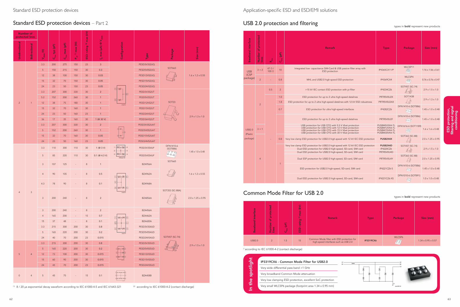
62 63
ESD
pro
tect
ion,
fil
terin
g a
nd s
igna
l co
nditi
onin
g
Standard ESD protection devices – Part 2
Standard ESD protection devices
Number of protected lines
VR
WM (
V)
Clin
e ty
p (
pF)
Clin
e m
ax (
pF)
PP
P [1
] max
(W
)
ESD
rat
ing
[2] m
ax (
kV)
I R m
ax (
µA)
@ V
RW
M
Co
nfig
urat
ion
Typ
e
Pac
kag
e
Size
(m
m)
Uni
dir
ecti
ona
l
Bid
irec
tio
nal
2 1
3.3 200 275 150 23 3 PESD3V3S2UQ
SOT663
1.6 x 1.2 x 0.55
5 150 215 150 30 0.3 PESD5V0S2UQ
12 38 100 150 30 0.03 PESD12VS2UQ
15 32 70 150 30 0.05 PESD15VS2UQ
24 23 50 150 23 0.05 PESD24VS2UQ
3.3 207 300 330 30 2 PESD3V3S2UT
SOT23
2.9 x 1.3 x 1.0
5.2 152 200 260 30 1 PESD5V2S2UT
12 38 75 180 30 1 PESD12VS2UT
15 32 70 160 30 1 PESD15VS2UT
24 23 50 160 23 1 PESD24VS2UT
36 17 35 160 30 1 (@ 30 V) PESD36VS2UT
3.3 207 300 330 30 2 PESD3V3S2UAT
5 152 200 260 30 1 PESD5V0S2UAT
15 32 70 160 30 0.05 PESD15VS2UAT
24 23 50 160 23 0.05 PESD24VS2UAT
4 3
3.3 110 300 110 30 1 (@ 3 V) PESD3V3S4UFDFN1410-6 (SOT886)
1.45 x 1.0 x 0.48
5 85 220 110 30 0.1 (@ 4.3 V) PESD5V0S4UF
3 107 125 - 8 1 BZA956ASOT665
1.6 x 1.2 x 0.554 90 105 - 8 0.5 BZA962A
4.3 78 90 - 8 0.1 BZA968A
3 200 240 - 8 2 BZA856A
SOT353 (SC-88A)
2.0 x 1.25 x 0.95
3 200 240 - 8 2 BZA456A
SOT457 (SC-74)
2.9 x 1.5 x 1.0
4 165 200 - 15 0.7 BZA462A
15 37 48 - 8 0.1 BZA420A
3.3 215 300 200 30 0.8 PESD3V3S4UD
5 165 220 200 30 0.2 PESD5V0S4UD
24 40 70 200 23 0.015 PESD24VS4UD
5 4
3.3 215 300 200 30 0.8 PESD3V3S5UD
5 165 220 200 30 0.2 PESD5V0S5UD
12 73 100 200 30 0.015 PESD12VS5UD
15 60 90 200 30 0.015 PESD15VS5UD
24 45 70 200 23 0.015 PESD24VS5UD
0 4 5 45 75 - 15 0.1 BZA408B
bra004
1
2
3
006aaa156
61
52
43
mse214
1
3
2 5
6
4
mse216
1
3
2 5
6
4
[1] 8 / 20 µs exponential decay waveform according to IEC 61000-4-5 and IEC 61643-321 [2] according to IEC 61000-4-2 (contact discharge)
Application-specific ESD and ESD/EMI solutions
USB 2.0 protection and filtering
Bas
eban
d in
terf
ace
Num
ber
of
pro
tect
ed
lines
Rlin
e
Clin
e (p
F)
Remark Type Package Size (mm)
USB(CSP
package)
3 + 2 47 Ω / 100 Ω 10 Integrated low- capacitance SIM-Card & USB passive filter array with
ESD protection IP4365CX11/P WLCSP11
1.16 x 1.56 x 0.61
2 - 0.8 MHL and USB2.0 high-speed ESD-protection IP4369CX4WLCSP4
0.76 x 0.76 x 0.47
USB2.0
(Plastic
package)
2
0.5 2 >15 kV IEC contact ESD protection with pi-filter IP4234CZ6SOT457 (SC-74)
2.9 x 1.5 x 1.0
-
1.0 ESD protection for up to 2 ultra high-speed datalines PRTR5V0U2X SOT143B2.9 x 1.3 x 1.0
1.8 ESD protection for up to 2 ultra high-speed datalines with 12 kV ESD robustness PRTR5V0U2AX
0.7 ESD protection for ultra high-speed interfaces IP4282CZ6DFN1410-6 (SOT886)
1.45 x 1.0 x 0.48
ESD protection for up to 2 ultra high-speed datalines PRTR5V0U2FDFN1410-6 (SOT886)
1.45 x 1.0 x 0.48
3 + 1
USB protection for USB OTG with 5.5 V Vbat protection PUSBM5V5X4-TL DFN1616-6 (SOT1189)1.6 x 1.6 x 0.48USB protection for USB OTG with 12 V Vbat protection PUSBM12VX4-TL
USB protection for USB OTG with 15 V Vbat protection PUSBM15VX4-TLUSB protection for USB OTG with 30 V Vbat protection PUSBM30VX4-TL
4
0.8 Very low clamp ESD protection for USB2.0 high-speed with 12 kV IEC ESD protection PUSB2X4XSOT363 (SC-88)
2.0 x 1.25 x 0.95
1
Very low clamp ESD protection for USB2.0 high-speed with 12 kV IEC ESD protection PUSB2X4D SOT457 (SC-74)2.9 x 1.5 x 1.0Dual ESD protection for USB2.0 high-speed, SD-card, SIM card IP4220CZ6
Dual ESD protection for USB2.0 high-speed, SD-card, SIM card PRTR5V0U4D
Dual ESP protection for USB2.0 high-speed, SD-card, SIM card PRTR5V0U4Y SOT363 (SC-88)
2.0 x 1.25 x 0.95
ESD protection for USB2.0 high-speed, SD-card, SIM card IP4221CZ6-SDFN1410-6 (SOT886)
1.45 x 1.0 x 0.48
Dual ESD protection for USB2.0 high-speed, SD-card, SIM-card IP4221CZ6-XSDFN1010-6 (SOT891)
1.0 x 1.0 x 0.48
types in bold represent new products
Bas
eban
d in
terf
ace
Num
ber
of
pro
tect
ed
lines
Clin
e (p
F)
ESD
rat
ing
[1] m
ax (
kV)
Remark Type Package Size (mm)
USB2.0 2 1.5 15 Common Mode filter with ESD protection for high-speed interfaces such as USB 2.0 IP3319CX6
WLCSP61.34 x 0.95 x 0.57
Common Mode Filter for USB 2.0types in bold represent new products
[1 according to IEC 61000-4-2 (contact discharge)In
the
sp
otl
ight IP3319CX6 - Common Mode Filter for USB2.0
Very wide differential pass band >1 GHz
Very broadband Common Mode attenuation
Very low clamping ESD protection, excellent SoC protection
Very small WLCSP6 package (footprint area 1.34 x 0.95 mm)
64 65
ESD
pro
tect
ion,
fil
terin
g a
nd s
igna
l co
nditi
onin
g
Bas
eban
d in
terf
ace
Num
ber
of
pro
tect
ed li
nes
Clin
e (p
F)
ESD
rat
ing
max
(kV
)
Rd
yn (Ω
)
Remark Type Package Size (mm)
USB3.0 - 5 Gbps 4
0.55 8
0.3 / 0.4
ESD protection for ultra high-speed interfaces
IP4292CZ10-TBR DFN2510A-10 (SOT1176)
2.5 x. 1.0 x 0.480.5 10
IP4294CZ10-TBR
PUSB3F96
USB3.1 - 10 Gbps
60.29 15 0.27 PUSB3FR6 DFN2111-7 (SOT1358)
2.1 x 1.1 x 0.480.27 15 0.5 PUSB3TB6
4 0.29 15 0.27 PUSB3FR4
DFN2510A-10 (SOT1176)
2.5 x. 1.0 x 0.48
1
0.18 10 0.5 PESD5V0R1BSF DSN0603-2 (SOD962)
0.6 x 0.3 x 0.30.22 15 0.36 PESD5V0H1BSF
0.26 20 0.35 PESD5V0C1BSF
0.35 20 0.18 PESD5V0C1USF
Application-specific ESD and ESD/EMI solutions
USB 3.x and eSATA protection and filteringtypes in bold represent new products
NXP paves the way for USB Type-C connector
PUSB3FR4 and the new Type-C connector The perfect match. PUSB3FR4 supports protection and filtering for the new Type-C connector, in order to enable flawless direction-agnostic, faster charging and the smal-lest solution to support SuperSpeed USB.
USB 3.1 introduces data rates up to 10 GbpsAs shown in the eye diagram, NXP offers protection, which supports data rates up to 10 Gbps with low capaci-tance and optimized package layouts.
USB Type-C receptacle
PUSB3FR4 on standard FR4 testboard
USB Type-C plug PUSB3FR4 routing diagram
PCMFxDFN1 offers the largest bandwith on Common Mode suppression The superior system-level protection is shown in the lower TLP clamping voltage
PCMFxUSB30 Only test board
Bas
eban
d in
terf
ace
Num
ber
of
pro
tect
ed li
ne
pai
rs
Typ
e
Diff
eren
tial
Mo
de
3dB
fr
eque
ncy
Co
mm
on
Mo
de
reje
ctio
n 80
0 M
Hz
- 2.
4 G
Hz
Cd t
ypic
al
VR
WM
ESD
rat
ing
Cha
nnel
ser
ies
resi
stan
ce
Package Size (mm)
USB3.x
1
PCMF1USB30
>7 GHz
>12
0.3 5 15 3
WLCSP50.8 x 1.2 x 0.5
2WLCSP10
1.6 x 1.2 x 0.5
3WLCSP15
2.4 x 1.2 x 0.5
1
PESD1USB30 ESD protection only
WLCSP50.8 x 1.2 x 0.5
2WLCSP10
1.6 x 1.2 x 0.5
3WLCSP15
2.4 x 1.2 x 0.5
Common Mode Filter for USB 3.xtypes in bold represent new products
[1 according to IEC 61000-4-2 (contact discharge)
Common Mode suppression performance (for various ferrite and ceramic filters) Clamping performance of PCMF compared to silicon
USB 3.x 5 Gbps eye diagrams
Application-specific ESD and ESD/EMI solutions
NXPs Common Mode Filter offer:
Best in class system-level protection due to deep
snap-back and very low dynamic resistance
Very wide-band Common Mode rejection to cover all
critical frequencies
Improved RF performance and small footprint compared
to separate ESD/CMF solutions
Protection for MIPI CSI, DSI, USB3.x, and HDMI
66 67
ESD
pro
tect
ion,
fil
terin
g a
nd s
igna
l co
nditi
onin
g
Application-specific ESD and ESD/EMI solutionsApplication-specific ESD and ESD/EMI solutions
Bas
eban
d
inte
rfac
e
Num
ber
of
pro
tect
ed li
nes
Clin
e (p
F) Remark Type Package Size (mm)
LAN
1 0.6
Ethernet ESD protection VRWM = 3.3 V PESD3V3U1UT
SOT23
2.9 x 1.3 x 1.0
Ethernet ESD protection VRWM = 5.0 V PESD5V0U1UT
Ethernet ESD protection VRWM = 12 V PESD12VU1UT
Ethernet ESD protection VRWM = 15 V PESD15VU1UT
Ethernet ESD protection VRWM = 24 V PESD24VU1UT
4 1
Ethernet line-surge ESD protection IP4233CZ6 SOT363 (SC-88)
2.0 x 1.25 x 0.95
Ethernet ESD protection IP4220CZ6SOT457 (SC-74)
2.9 x 1.5 x 1.0
Ethernet protectiontypes in bold represent new products
types in bold represent new productsHDMI and memory-card signal conditioning
Inte
rfac
e
Num
ber
of
pro
tect
ed li
nes
Buf
fer
Leve
l shi
fer
Clin
e (p
F)
Res
isto
r (Ω
)
LDO
Remark Type Package Size (mm)
HDMI tx
5
yes yes
- internal - Fully integrated for HDMI control lines including buffer for DDC, CEC, and Hot Plug module IP4791CZ12
DFN2521-12 (SOT1156)
2.5 x 2.1 x 0.48
10 1.75 k, 100 k HDMI, DDC, CEC, Hot Plug ESD protection and biasing IP4310CX8/P
WLCSP8
1.16 x 1.16 x 0.61
13100 Ω
differential impedance
internal
CEC LDO. 5 V
LDO
Fully integrated HDMI source solution with current limiter, buffer, and level shifter for DDC, CEC, and Hot Plug
IP4786CZ32DFN5050-32 (SOT617)
5.0 x 5.0 x 0.85Fully integrated HDMI sink solution with buffer, and level
shifter for DDC, CEC, and Hot Plug
Fully integrated HDMI source solution with enhanced ESD protection, current limiter, buffer, and level shifter for DDC,
CEC, and Hot Plug
Fully integrated HDMI source solution with small package, current limiter, buffer, and level shifter for DDC, CEC, and
Hot PlugIP4786CZ32S
DFN4040-32 (SOT1318-1)
4.0 x 4.0 x 0.50
HDMI2.0 13 yes yes100 Ω
differential impedance
integrated -
Fully integrated HDMI source solution with current limiter, buffer, and level shifter for DDC, CEC, and Hot Plug
IP4786CZ32
DFN5050-32 (SOT617)
5.0 x 5.0 x 0.85
IP4787CZ32 5.0 x 5.0 x 0.85
Fully integrated HDMI source solution with enhanced ESD protection, current limiter, buffer, and level shifter for DDC,
CEC, and Hot PlugIP4788CZ32 5.0 x 5.0 x 0.85
Fully integrated HDMI source solution in a small package with current limiter, buffer, and level shifter for DDC, CEC,
and Hot PlugIP4786CZ32S
DFN4040-32 (SOT1318-1)
4.0 x 4.0 x 0.5
SD3.0 6 yes yes - internal
- SD 3.0-compliant memory card with integrated dual voltage- level translator with EMI filter and ESD protection IP4856CX25/C
WLCSP25
2.4 x 2.4 x 0.4
1.8 V LDO
Fully integrated SD 3.0 card level shifter with buffer technology, LDO, and EMI filter
IP4855CX25
WLCSP25
2.4 x 2.4 x 0.4
IP4755CZ24
DFN5535-24 (SOT815)
3.5 x 5.5 x 0.85
[1 according to IEC 61000-4-2 (contact discharge)
Common Mode Filter for video interfacesB
aseb
and
inte
rfac
e
Num
ber
of
pro
tect
ed li
ne
pai
rs u
nid
irec
tio
nal
Num
ber
of
pro
tect
ed li
ne
pai
rs b
idir
ecti
ona
l
Typ
e
Dif
fere
ntia
l Mo
de
3 d
B f
req
uenc
y (t
yp.)
Co
mm
on
Mo
de
inse
rtio
n lo
ss 8
00 M
Hz
- 2.
4 G
Hz
Cd p
F ty
pic
al
Vrw
m
ESD
rat
ing
[1] m
ax (
kV)
Cha
nnel
ser
ies
resi
stan
ce
Pac
kag
e
Size
(m
m)
MIPI D-PHY
2
0
PCMF2DFN1 >2 GHz
<-24 dB 0.8
5 15
5 Ω
DFN2520-9 (SOT1333)
2.5 x 2.0 x 0.48
3 PCMF3DFN1 >2 GHz
DFN4020-14 (SOT1334)
4.0 x 2.0 x 0.48
MIPI, HDMI
2 PCMF2DFN2
<3 GHz
<- 20 dB
0.7 2 Ω
DFN2520-9 (SOT1333)
2.5 x 2.0 x 0.48
3 PCMF3DFN2 <- 20 dB
DFN4020-14 (SOT1334)
4.0 x 2.0 x 0.48
types in bold represent new products
In t
he s
po
tlig
ht
4
5
12
11
7
8
10
9
aaa-007384
6
14
13
1
2
3
4
5
12
11
7
8
10
9
aaa-007384
6
14
13
1
2
3
PCMF-series: 2- and 3-line pair Common Mode filters for MIPI, HDMI
Very wide differential pass band >2 GHz
Very broadband Common Mode attenuation
Very low clamping ESD protection, excellent SoC protection
Very thin DFN plastic package (0.5 mm max)
68 69
ESD
pro
tect
ion,
fil
terin
g a
nd s
igna
l co
nditi
onin
g
Baseband interface
Number of protected
linesCline (pF) Remark Type Package Size (mm)
Display port 4
0.6 ESD protection for ultra high-speed interfaces IP4283CZ10-TBR
DFN2510A-10 (SOT1176) 2.5 x 1.0 x 0.480.55 ESD protection for ultra high-speed interfaces IP4292CZ10-TBR
0.5ESD protection for ultra high-speed interfaces IP4294CZ10-TBR
ESD protection for ultra high-speed interfaces PHDMI2F4
0.8 ESD protection for ultra high-speed interfaces IP4285CZ9-TBB
DFN2110-9 (SOT1178)
2.1 x 1.0 x 0.48
HDMI
2 0.7 ESD protection for ultra high-speed interfaces IP4282CZ6
DFN1410-6 (SOT886)
1.45 x 1.0 x 0.48
4
0.6 ESD protection for ultra high-speed interfaces IP4283CZ10-TBR
DFN2510A-10 (SOT1176)
2.5 x 1.0 x 0.48
0.8 ESD protection for ultra high-speed interfaces IP4285CZ9-TBB
DFN2110-9 (SOT1178)
2.1 x 1.0 x 0.48
0.55 ESD protection for ultra high-speed interfaces IP4292CZ10-TBR
DFN2510A-10 (SOT1176)2.5 x 1.0 x 0.48
0.5
ESD protection for ultra high-speed interfaces PHDMI2F4
ESD protection for ultra high-speed interfaces IP4294CZ10-TBR
LVDS 4
0.8 Very low clamp ESD protection with 12 kV IEC ruggedness
PUSB2X4D
SOT457 (SC-74)
2.9 x 1.5 x 1.0
0.8 Very low clamp ESD protection with 12 kV IEC ruggedness
PUSB2X4Y
SOT363 (SC-88)
2.0 x 1.25 x 0.95
Video interface protectiontypes in bold represent new products
Application-specific ESD and ESD/EMI solutions
PHDMI2F4 PESD HDMI application schematic
types in bold represent new products
Inte
rfac
e
Num
ber
of
pro
tect
ed li
nes
(Bid
irec
tio
nal)
VR
WM [V
]
Clin
e ty
p [p
F]
Clin
e m
ax [p
F]
ESD
rat
ing
[1]
max
[kV
] Configuration Type Package Size
NFC Antenna 1
18
0.28 0.45 10 PESD18VF1BSFDSN0603-2 (SOD962)
0.6 x 0.3 x 0.3
0.35 0.5 10 PESD18VF1BLDFN1006-2 (SOD882)
1.0 x 0.6 x 0.48
24
0.25 0.4 10 PESD24VF1BSFDSN0603-2 (SOD962)
0.6 x 0.3 x 0.3
0.3 0.45 10 PESD24VF1BLDFN1006-2 (SOD882)
1.0 x 0.6 x 0.48
NFC antenna protection
mse211
Application-specific ESD and ESD/EMI solutions
The highly linear diode capacitance, with very small variation, minimizes signal degradation
Diode capacitance versus bias voltage
Using tiny packages makes PCB design more flexible
Circuit diagram
[1 according to IEC 61000-4-2 (contact discharge)
Features
Bidirectional configuration, allowing operating voltages
up to 18 or 24 V
Very low capacitance, enabling easy design of the
antenna-matching circuit
Very small voltage dependency of the diode capacitance,
avoiding intermodulation distortion
Small form-factor packages of 1006 (0402 inch) and 0603
(0201 inch) standard size
Benefits
The phone’s NFC antenna is often integrated into the
battery cover or the battery itself and is connected to the
NFC tags via small contacts on the phone, creating an
entry point for ESD strikes that are potentially hazardous
to the NFC IC. These new NXP devices are optimized for
the requirements of th NFC system and ensure the best-
possible protection of the NFC IC.
PESD24VF1BSF – NFC antenna protection in DSN0603-2 package
High reverse standoff voltage VRWM=24 V
Ultra-low capacitance Cd typ = 0.25 pF
Very small voltage dependency of the capacitance
Ultra-small DSN0603-2 (SOD962) package (0.6 x 0.3 x 0.3 mm)
In t
he S
po
tlig
ht
mse211
70 71
ESD
pro
tect
ion,
fil
terin
g a
nd s
igna
l co
nditi
onin
g
Baseband interface
Number of protected
lines
Line small-signal equivalents
Digital interfaceclock speed
(MHz)Remark Type Package Size (mm)
Rline Cline (pF)
SIM card
3 + 2
47 Ω / 100 Ω
10
~20
Integrated low capacitance SIM-card passive filter array & USB ESD protection IP4365CX11
WLCSP11
1.16 x 1.56 x 0.61
3
20Integrated SIM-card EMI filter and ESD protection IP4064CX8/LF/P WLCSP8 1.41 x 1.41 x 0.65
Smaller size, integrated SIM-card EMI filter and ESD protection IP4364CX8/LF/P
1.16 x 1.16 x 0.6110 Smaller size, low-capacitance integrated SIM-card EMI
filter and ESD protection IP4366CX8/P
20 Integrated SIM-card EMI filter and ESD protection IP4264CZ8-20-TTLDFN1714-8 (SOT1166)
1.7 x 1.35 x 0.52
4 - 1 ~240
Quad-channel, low-capacitance ESD protection IP4221CZ6-SDFN1410-6 (SOT886)
1.0 x 1.0 x 0.48
Quad-channel, low-capacitance ESD protection IP4221CZ6-XSDFN1010-6 (SOT891)
1.0 x 1.0 x 0.48
SD-card / MMC
4 47 Ω / 13 kΩ / 56 kΩ 25 ~30 MMC ESD protection, pull-up resistors IP4051CX11/LF
WLCSP111.44 x 1.96 x 0.65
6
40 Ω 12 >52 (Mini) SD card/trans flash ESD protection, EMI filter IP4252CZ12-6-TTLDFN2514-12 (SOT1167)
2.5 x 1.35 x 0.53
40 Ω / 100 Ω 11 - 6-channel Micro-SD memory-card interface ESD protection filter IP4340CX15
WLCSP151.56 x 1.56 x 0.5
6 + 2 40 Ω 12 >52 (Mini) SD card/trans flash ESD protection, EMI filter IP4252CZ16-8-TTLDFN3314-16 (SOT1168)
3.3 x 1.35 x 0.53
SD 3.0 6 - 0.27 5000 6-line bidirectional ESD protection for ultra high-speed interfaces PUSB3TB6
DFN2111-7 (SOT1358)2.1 x 1.1 x 0.5
Memory- and SIM-card protection and filteringtypes in bold represent new products
Application-specific ESD and ESD/EMI solutions
LCD and camera protection and filteringB
aseb
and
in
terf
ace
Num
ber
of
pro
tect
ed li
nes
Line small-signal equivalents
Dig
ital
inte
rfac
ecl
ock
sp
eed
(MH
z)
Inse
rtio
n lo
ss S
21~
-3
dB
(M
Hz)
Typ
e
Pac
kag
e
Size
(mm
)
Rlin
e (Ω
)
Clin
e (p
F)
L line
(nH
)
LCD display,camera,keypad
245
40 - ~50 145 PEMI2STD/HT SOT665
1.6 x 1.2 x 0.515 - ~125 376 PEMI2STD/HE
200 40 - ~40 119 PEMI2STD/WT
4
1543 18 ~60 175 IP3253CZ8-4-TTL
DFN1714-8(SOT1166)
1.7 x 1.35 x 0.52
50 18 ~50 145 IP3254CZ8-4-TTL
40 18 - ~100 300 IP4252CZ8-4 -TTL
10045 - ~40 130 IP4254CZ8-4-TTL
15 - ~110 330 IP4251CZ8-4-TTL
200 45 - ~35 110 IP4253CZ8-4-TTL
100 54 - ~35 98 PEMI4CSP/RW
WLCSP10
1.56 x 1.05 x 0.61
6
1550 18 ~50 145 IP3254CZ12-6-TTL
DFN2514-12(SOT1167)
2.5 x 1.35 x 0.53
43 18 ~60 175 IP3253CZ12-6-TTL
40 18 - ~100 300 IP4252CZ12-6-TTL
10045 - ~40 130 IP4254CZ12-6-TTL
15 - ~110 330 IP4251CZ12-6-TTL
200 45 - ~35 110 IP4253CZ12-6-TTL
100 54 - ~35 98 PEMI6CSP/RW
WLCSP15
2.36 x 1.05 x 0.61
7 70 25 - ~75 220 IP4337CX18/LF
WLCSP18
1.96 x 1.61 x 0.61
8
1543 18 ~60 175 IP3253CZ16-8-TTL
DFN3314-16 (SOT1168)
3.3 x 1.35 x 0.53
50 18 ~50 145 IP3254CZ16-8-TTL
40 18 - ~100 300 IP4252CZ16-8-TTL
10045 - ~40 130 IP4254CZ16-8-TTL
15 - ~110 330 IP4251CZ16-8-TTL
200 45 - ~35 110 IP4253CZ16-8-TTL
100 54 - ~35 98 PEMI8CSP/RW/P
WLCSP20
3.16 x 1.05 x 0.61
10
70 25 - ~75 220 IP4338CX24/LFWLCSP24
1.96 x 2.01 x 0.61
1000 50 - ~7 22 IP4035CX24/LF 2.41 x 2.41 x 0.65
200 50 - ~35 105 IP4041CX25/LF
WLCSP25
2.41 x 2.41 x 0.65
types in bold represent new productsAudio interface protection and filtering
Application-specific ESD and ESD/EMI solutions
Battery and charger protectionBaseband interface
Number of protected lines
Cline (pF) Diode voltage Remark Type Package Size (mm)
Battery & charger
protection1
180 Breakdown 16 V Power diode IP4085CX4 WLCSP4 0.91 x 0.91 x 0.65
160 Breakdown 16 V Power diode IP4386CX40.76 x 0.76 x 0.61
290 Breakdown 10 V Power diode IP4387CX4
160 VRWM = 12 V Power diode PESD12VS1UJ
SOD323F (SC-90)
1.7 x 1.25 x 0.7
160 VRWM = 12 V Power diode PESD12VS1UA
SOD323 (SC-76)
1.7 x 1.25 x 0.95
480 VRWM = 5 V Power diode PESD5V0S1UJ
SOD323F (SC-90)
1.7 x 1.25 x 0.7
480 VRWM = 5 V Power diode PESD5V0S1UA
SOD323 (SC-76)
1.7 x 1.25 x 0.95
Baseband interface
Number of
protected lines
Line small-signal equivalents
Remark Type Package Size (mm)Rline Cline (pF)
Audio
2
0.9 Ω 290 Low-ohmic speaker (<~8 Ω) IP4047CX6/LF WLCSP6
1.56 x 1.01 x 0.65
10 Ω 200 Low-ohmic speaker (>~8 Ω) IP4048CX5/LF WLCSP5
0.91 x 1.28 x 0.6568 Ω 110 Single-ended or differential microphone IP4049CX5/LF
5 2.9 kΩ, 1 kΩ / 10 Ω - 5-channel filter interface with integrated RC filters and biasing network for audio interfaces IP4327CX15
WLCSP15
1.05 x 2.36 x 0.61
IP3253CZ8-4TTL – LCD and camera display protection in DFN1714-8
Very wide pass-band 175 MHz
Filters and protects 4, 6 or 8 data lines
Very low clamping ESD protection, 15 kV IEC ESD ruggedness
Very low series resistance of only 8 Ω
Leadless DFN1714-8 (SOT1166) package with a height of only 0.52 mm
In t
he S
po
tlig
ht
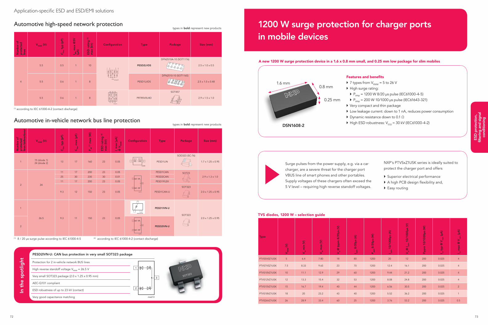
72 73
ESD
pro
tect
ion,
fil
terin
g a
nd s
igna
l co
nditi
onin
g
Automotive high-speed network protectionN
umbe
r of
pr
otec
ted
lin
es
VRWM (V)
Clin
e ty
p (
pF)
I RM m
ax @
3V
(µA
)
ESD
rat
ing
[1]
max
(kV
) Configuration Type Package Size (mm)
4
5.5 0.5 1 10 PESD2LVDS
DFN2510A-10 (SOT1176)
2.5 x 1.0 x 0.5
5.5 0.6 1 8 PESD1LVDS
DFN2510-10 (SOT1165)
2.5 x 1.0 x 0.48
5.5 0.6 1 8 PRTR5V0U4D
SOT457
2.9 x 1.5 x 1.0
2 4
3, 8 001aai619
1 5
001aag273
1 2 3
6 5 4
Application-specific ESD and ESD/EMI solutions
(1) according to IEC 61000-4-2 (contact discharge)
types in bold represent new products
Num
ber
of
prot
ecte
d
lines
bid
irec
tion
al
VRWM (V)
Clin
e ty
p (
pF)
Clin
e m
ax (
pF)
PP
P [1
] max
(W
)
ESD
rat
ing
[2]
max
(kV
)
I r max
[µA
] @
VR
WM
Configuration Type Package Size (mm)
1 15 (diode 1)24 (diode 2) 13 17 160 23 0.05 PESD1LIN
SOD323 (SC-76)
1.7 x 1.25 x 0.95
2 24
11 17 200 23 0.05 PESD1CAN SOT23
2.9 x 1.3 x 1.025 30 230 30 0.01 PESD2CAN
11 17 200 23 0.05 PESD1FLEX
9.3 12 150 23 0.05 PESD1CAN-U
SOT323
2.0 x 1.25 x 0.95
1
26.5 9.3 11 150 23 0.05
PESD1IVN-U
SOT3232.0 x 1.25 x 0.95
2 PESD2IVN-U
Automotive in-vehicle network bus line protection
mse213
1
2
3
mse213
1
2
3
bra526
15 V 24 V1 2
[1] 8 / 20 µs surge pulse according to IEC 61000-4-5 [2] according to IEC 61000-4-2 (contact discharge)
types in bold represent new products
PESD2IVN-U: CAN bus protection in very small SOT323 package
Protection for 2 in-vehicle network BUS lines
High reverse standoff voltage VRWM = 26.5 V
Very small SOT323 package (2.0 x 1.25 x 0.95 mm)
AEC-Q101 compliant
ESD robustness of up to 23 kV (contact)
Very good capacitance matching
In t
he s
po
tlig
ht
mse213
1
2
3
1200 W surge protection for charger ports in mobile devices
Features and benefits
7 types from VRWM = 5 to 26 V
High surge rating:
PPPM = 1200 W 8/20 µs pulse (IEC61000-4-5)
PPPM = 200 W 10/1000 µs pulse (IEC61643-321)
Very compact and thin package
Low leakage current: down to 1 nA, reduces power consumption
Dynamic resistance down to 0.1 Ω
High ESD robustness: VESD = 30 kV (IEC61000-4-2)
A new 1200 W surge protection device in a 1.6 x 0.8 mm small, and 0.25 mm low package for slim mobiles
1.6 mm
DSN1608-2
0.8 mm
0.25 mm
NXP’s PTVSxZ1USK series is ideally suited to
protect the charger port and offers
Superior electrical performance
A high PCB design flexibility and,
Easy routing
Surge pulses from the power supply, e.g. via a car
charger, are a severe threat for the charger port
VBUS line of smart phones and other portables.
Supply voltages of these chargers often exceed the
5 V level – requiring high reverse standoff voltages.
TVS diodes, 1200 W – selection guide
Type
VR
WM
(V)
Vb
r m
in (V
)
Vb
r m
ax (V
)
Vcl
@ Ip
pm
8/2
0µs
(V)
I pp
m 8
/20µ
s (A
)
Pp
pm
8/2
0µs
(W)
I pp
m 1
0/10
00µs
(A)
Vcl
@ I p
pm 1
0/10
00µs
(V)
Pp
pm
10/
1000
µs (W
)
I rm ty
p @
Vrw
m (µ
A)
I rm m
ax @
Vrw
m (µ
A)
PTVS5V0Z1USK 5 6.4 7.80 18 80 1200 20 12 200 0.025 4
PTVS7V5Z1USK 7.5 8.33 9.65 23 70 1200 12.4 16.1 200 0.025 4
PTVS10VZ1USK 10 11.1 12.9 29 60 1200 9.44 21.2 200 0.025 4
PTVS12VZ1USK 12 13.3 15.4 32 53 1200 8.08 24.8 200 0.025 4
PTVS15VZ1USK 15 16.7 19.4 40 44 1200 6.56 30.5 200 0.025 2
PTVS18VZ1USK 18 20 23.2 43 40 1200 5.52 36.2 200 0.025 1
PTVS26VZ1USK 26 28.9 33.4 60 25 1200 3.76 53.2 200 0.025 0.5
74 75
ESD
pro
tect
ion,
fil
terin
g a
nd s
igna
l co
nditi
onin
g
TVS diodes
TVS diodes, 400 W
Po
wer
(W
) (1
0/10
00
µs w
avef
orm
) [1
]
VR
WM (
V)
VB
R m
in (
V)
@ I
R
VB
R t
yp (
V)
@ I
R
VB
R m
ax (
V)
@ I
R
I R (
mA
)
VC
L max
[1] (V
) @ I PP
I PP [1
] (A
)
I RM t
yp (
µA)
@
VR
WM
I RM m
ax (µ
A) @
V
RWM
Type (Tj max = 150 °C)
Type (Tj max = 185 °C) Package Size (mm)
350 3.5 5.20 5.60 6.00 10 8.0 43.8 5 600 PTVS3V3S1UR PTVS3V3S1UTR
SOD123W
2.6 x 1.7 x 1.0
400
5.0 6.40 6.70 7.00 10 9.2 43.5 5 400 PTVS5V0S1UR PTVS5V0S1UTR
6.0 6.67 7.02 7.37 10 10.3 38.8 5 400 PTVS6V0S1UR PTVS6V0S1UTR
6.5 7.22 7.60 7.98 10 11.2 35.7 5 250 PTVS6V5S1UR PTVS6V5S1UTR
7.0 7.78 8.20 8.60 10 12.0 33.3 3 100 PTVS7V0S1UR PTVS7V0S1UTR
7.5 8.33 8.77 9.21 1 12.9 31.0 0.2 50 PTVS7V5S1UR PTVS7V5S1UTR
8.0 8.89 9.36 9.83 1 13.6 29.4 0.03 25 PTVS8V0S1UR PTVS8V0S1UTR
8.5 9.44 9.92 10.40 1 14.4 27.8 0.01 10 PTVS8V5S1UR PTVS8V5S1UTR
9.0 10.00 10.55 11.10 1 15.4 26.0 0.005 5 PTVS9V0S1UR PTVS9V0S1UTR
10 11.10 11.70 12.30 1 17.0 23.5 0.005 2.5 PTVS10VS1UR PTVS10VS1UTR
11 12.20 12.85 13.50 1 18.2 22.0 0.005 2.5 PTVS11VS1UR PTVS11VS1UTR
12 13.30 14.00 14.70 1 19.9 20.1 0.005 2.5 PTVS12VS1UR PTVS12VS1UTR
13 14.40 15.15 15.90 1 21.5 18.6 0.001 0.1 PTVS13VS1UR PTVS13VS1UTR
14 15.60 16.40 17.20 1 23.2 17.2 0.001 0.1 PTVS14VS1UR PTVS14VS1UTR
15 16.70 17.60 18.50 1 24.4 16.4 0.001 0.1 PTVS15VS1UR PTVS15VS1UTR
16 17.80 18.75 19.70 1 26.0 15.4 0.001 0.1 PTVS16VS1UR PTVS16VS1UTR
17 18.90 19.90 20.90 1 27.6 14.5 0.001 0.1 PTVS17VS1UR PTVS17VS1UTR
18 20.00 21.00 22.10 1 29.2 13.7 0.001 0.1 PTVS18VS1UR PTVS18VS1UTR
20 22.20 23.35 24.50 1 32.4 12.3 0.001 0.1 PTVS20VS1UR PTVS20VS1UTR
22 24.40 25.60 26.90 1 35.5 11.3 0.001 0.1 PTVS22VS1UR PTVS22VS1UTR
24 26.70 28.10 29.50 1 38.9 10.3 0.001 0.1 PTVS24VS1UR PTVS24VS1UTR
26 28.90 30.40 31.90 1 42.1 9.5 0.001 0.1 PTVS26VS1UR PTVS26VS1UTR
28 31.10 32.80 34.40 1 45.4 8.8 0.001 0.1 PTVS28VS1UR PTVS28VS1UTR
30 33.30 35.10 36.80 1 48.4 8.3 0.001 0.1 PTVS30VS1UR PTVS30VS1UTR
33 36.70 38.70 40.60 1 53.3 7.5 0.001 0.1 PTVS33VS1UR PTVS33VS1UTR
36 40.00 42.10 44.20 1 58.1 6.9 0.001 0.1 PTVS36VS1UR PTVS36VS1UTR
40 44.40 46.80 49.10 1 64.5 6.2 0.001 0.1 PTVS40VS1UR PTVS40VS1UTR
43 47.80 50.30 52.80 1 69.4 5.8 0.001 0.1 PTVS43VS1UR PTVS43VS1UTR
45 50.00 52.65 55.30 1 72.7 5.5 0.001 0.1 PTVS45VS1UR PTVS45VS1UTR
48 53.30 56.10 58.90 1 77.4 5.2 0.001 0.1 PTVS48VS1UR PTVS48VS1UTR
51 56.70 59.70 62.70 1 82.4 4.9 0.001 0.1 PTVS51VS1UR PTVS51VS1UTR
54 60.00 63.15 66.30 1 87.1 4.6 0.001 0.1 PTVS54VS1UR PTVS54VS1UTR
58 64.40 67.80 71.20 1 93.6 4.3 0.001 0.1 PTVS58VS1UR PTVS58VS1UTR
60 66.70 70.20 73.70 1 96.8 4.1 0.001 0.1 PTVS60VS1UR PTVS60VS1UTR
64 71.10 74.85 78.60 1 103.0 3.9 0.001 0.1 PTVS64VS1UR PTVS64VS1UTR
TVS diodes, 24 / 40 W
TVS diodesP
ow
er (
W)
(10
/ 10
00
µs w
avef
orm
) [1
]
VR
WM (
V)
VB
R m
in (
V)
@ I
R
VB
R t
yp (
V)
@ I
R
VB
R m
ax (
V)
@ I
R
I R (
mA
)
ESD
rat
ing
[1] m
ax (
kV)
Clin
e ty
p (
pF)
VC
L m
ax [1
] (V
) @
IP
P
I PP [1
] (A
)
I RM m
ax (
µA)
@ V
RW
M
Configuration Type Package Size (mm)
24
3 5.32 5.6 5.88 20 30 210 8 3 5 MMBZ5V6AL
SOT23 2.9 x 1.3 x 1.0
3 5.89 6.2 6.51 1 30 175 8.7 2.76 0.2 MMBZ6V2AL
4.5 6.48 6.8 7.14 1 30 150 9.6 2.5 0.3 MMBZ6V8AL
6 8.65 9.1 9.56 1 30 155 14 1.7 0.1 MMBZ9V1AL
6.5 9.5 10 10.5 1 30 130 14.2 1.7 0.02 MMBZ10VAL
40
8.5 11.4 12 12.6 1 30 110 17 2.35 0.005 MMBZ12VAL
12 14.25 15 15.75 1 30 85 21 1.9 0.005 MMBZ15VAL
14.5 17.1 18 18.9 1 30 70 25 1.6 0.005 MMBZ18VAL
17 19 20 21 1 30 65 28 1.4 0.005 MMBZ20VAL
22 25.65 27 28.35 1 30 48 40 1 0.005 MMBZ27VAL
26 31.35 33 34.65 1 30 45 46 0.87 0.005 MMBZ33VAL
8.5 11.4 12 12.6 1 30 110 17 2.35 0.005 MMBZ12VDL
12.8 14.3 15 15.8 1 30 85 21.2 1.9 0.005 MMBZ15VDL
14.5 17.1 18 18.9 1 30 70 25 1.6 0.005 MMBZ18VCL
17 19 20 21 1 30 65 28 1.4 0.005 MMBZ20VCL
22 25.65 27 28.35 1 30 48 38 1 0.005 MMBZ27VCL
26 31.35 33 34.65 1 30 45 46 0.87 0.005 MMBZ33VCLbra004
1
2
3
(1) 10 / 1000 μs according to IEC 61643-321 (2) according to IEC 61000-4-2 (contact discharge)
TVS diodes for mobile applications
Po
wer
(W
) (1
0 /
1000
µs
wav
efo
rm)
[1]
VR
WM (
V)
VB
R m
in (
V)
@ I
R
VB
R t
yp (
V)
@ I
R
VB
R m
ax (
V)
@ I
R
I R (
mA
)
VC
L m
ax [1
] (V
) @
IP
P
I PP [1
] (A
)
I RM t
yp (
µA)
@ V
RW
M
I RM m
ax (
μA)
@ V
RW
M
Type Package Size (mm)
300
7.5 8.33 8.77 9.21 1 12.9 23.3 0.3 50 PTVS7V5U1UPA
DFN2020-3 (SOT1061)
2.0 x 2.0 x 0.62
10 11.1 11.7 12.3 1 17 17.6 0.008 2.5 PTVS10VU1UPA
12 13.3 14 14.7 1 19.9 15.1 0.005 2.5 PTVS12VU1UPA
15 16.7 17.6 18.5 1 24.4 12.3 0.001 0.1 PTVS15VU1UPA
18 20 21 22.1 1 29.2 10.3 0.001 0.1 PTVS18VU1UPA
26 28.9 30.4 31.9 1 42.1 7 0.001 0.1 PTVS26VU1UPA
(1) 10 / 1000 μs according to IEC 61643-321
PTVSxU1UPA series: 300 W surge protection in DFN2020-3 package
Series of 6 types from VRWM= 7.5 to 26 V
Peak pulse power of 300 W for 10 / 1000 µs pulse
Small package size of 2.0 x 2.0 mm
Very low package height of 0.62 mm typ
Charger-port protection in mobile devices
In t
he s
po
tlig
ht
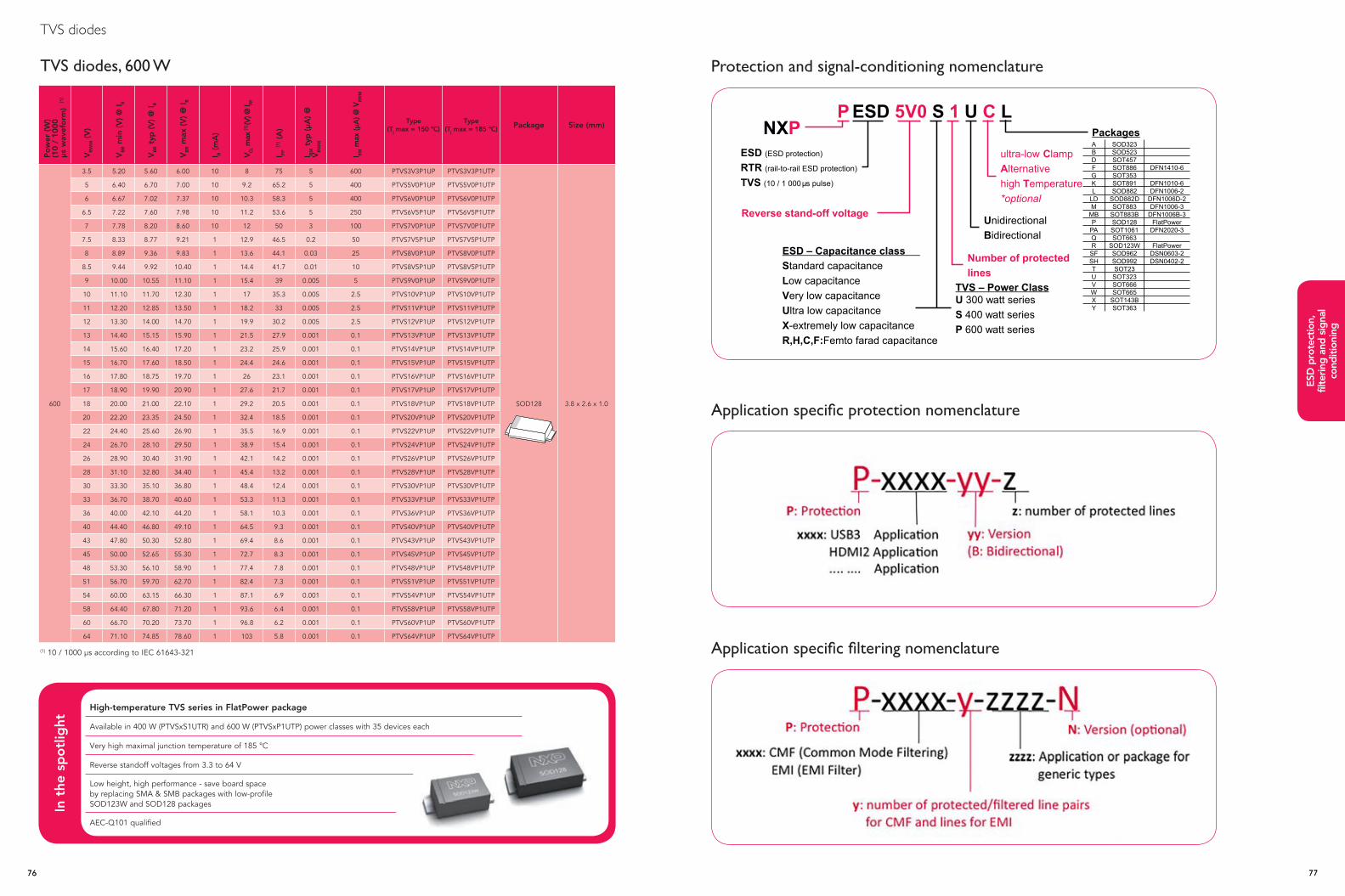
76 77
ESD
pro
tect
ion,
fil
terin
g a
nd s
igna
l co
nditi
onin
g
7776 7776
Protection and signal-conditioning nomenclatureNomenclature - Protection devices
NXP ESD (ESD protection)
RTR (rail-to-rail ESD protection)
TVS (10 / 1 000 s pulse)
ESD – Capacitance class Standard capacitance Low capacitance Very low capacitance Ultra low capacitance X-extremely low capacitance R,H,C,F:Femto farad capacitance
Number of protected lines
Packages
Unidirectional Bidirectional
P ESD 5V0 S 1 U C L
Reverse stand-off voltage
TVS – Power Class U 300 watt series S 400 watt series P 600 watt series
ultra-low Clamp Alternative high Temperature *optional
A SOD323 B SOD523 D SOT457 F SOT886 DFN1410-6 G SOT353 K SOT891 DFN1010-6 L SOD882 DFN1006-2
LD SOD882D DFN1006D-2 M SOT883 DFN1006-3
MB SOT883B DFN1006B-3 P SOD128 FlatPower
PA SOT1061 DFN2020-3 Q SOT663 R SOD123W FlatPower
SF SOD962 DSN0603-2 SH SOD992 DSN0402-2 T SOT23 U SOT323 V SOT666 W SOT665 X SOT143B Y SOT363
Application specific protection nomenclature
Application specific filtering nomenclature
TVS diodes, 600 W
TVS diodesP
ow
er (
W)
(1
0 /
1000
µs
wav
efo
rm)
[1]
VR
WM (
V)
VB
R m
in (
V)
@ I
R
VB
R t
yp (
V)
@ I
R
VB
R m
ax (
V)
@ I
R
I R (
mA
)
VC
L max
[1] (V
) @ I PP
I PP [1
] (A
)
I RM t
yp (
µA)
@
VR
WM
I RM m
ax (µ
A) @
VRW
M
Type (Tj max = 150 °C)
Type (Tj max = 185 °C) Package Size (mm)
600
3.5 5.20 5.60 6.00 10 8 75 5 600 PTVS3V3P1UP PTVS3V3P1UTP
SOD128 3.8 x 2.6 x 1.0
5 6.40 6.70 7.00 10 9.2 65.2 5 400 PTVS5V0P1UP PTVS5V0P1UTP
6 6.67 7.02 7.37 10 10.3 58.3 5 400 PTVS6V0P1UP PTVS6V0P1UTP
6.5 7.22 7.60 7.98 10 11.2 53.6 5 250 PTVS6V5P1UP PTVS6V5P1UTP
7 7.78 8.20 8.60 10 12 50 3 100 PTVS7V0P1UP PTVS7V0P1UTP
7.5 8.33 8.77 9.21 1 12.9 46.5 0.2 50 PTVS7V5P1UP PTVS7V5P1UTP
8 8.89 9.36 9.83 1 13.6 44.1 0.03 25 PTVS8V0P1UP PTVS8V0P1UTP
8.5 9.44 9.92 10.40 1 14.4 41.7 0.01 10 PTVS8V5P1UP PTVS8V5P1UTP
9 10.00 10.55 11.10 1 15.4 39 0.005 5 PTVS9V0P1UP PTVS9V0P1UTP
10 11.10 11.70 12.30 1 17 35.3 0.005 2.5 PTVS10VP1UP PTVS10VP1UTP
11 12.20 12.85 13.50 1 18.2 33 0.005 2.5 PTVS11VP1UP PTVS11VP1UTP
12 13.30 14.00 14.70 1 19.9 30.2 0.005 2.5 PTVS12VP1UP PTVS12VP1UTP
13 14.40 15.15 15.90 1 21.5 27.9 0.001 0.1 PTVS13VP1UP PTVS13VP1UTP
14 15.60 16.40 17.20 1 23.2 25.9 0.001 0.1 PTVS14VP1UP PTVS14VP1UTP
15 16.70 17.60 18.50 1 24.4 24.6 0.001 0.1 PTVS15VP1UP PTVS15VP1UTP
16 17.80 18.75 19.70 1 26 23.1 0.001 0.1 PTVS16VP1UP PTVS16VP1UTP
17 18.90 19.90 20.90 1 27.6 21.7 0.001 0.1 PTVS17VP1UP PTVS17VP1UTP
18 20.00 21.00 22.10 1 29.2 20.5 0.001 0.1 PTVS18VP1UP PTVS18VP1UTP
20 22.20 23.35 24.50 1 32.4 18.5 0.001 0.1 PTVS20VP1UP PTVS20VP1UTP
22 24.40 25.60 26.90 1 35.5 16.9 0.001 0.1 PTVS22VP1UP PTVS22VP1UTP
24 26.70 28.10 29.50 1 38.9 15.4 0.001 0.1 PTVS24VP1UP PTVS24VP1UTP
26 28.90 30.40 31.90 1 42.1 14.2 0.001 0.1 PTVS26VP1UP PTVS26VP1UTP
28 31.10 32.80 34.40 1 45.4 13.2 0.001 0.1 PTVS28VP1UP PTVS28VP1UTP
30 33.30 35.10 36.80 1 48.4 12.4 0.001 0.1 PTVS30VP1UP PTVS30VP1UTP
33 36.70 38.70 40.60 1 53.3 11.3 0.001 0.1 PTVS33VP1UP PTVS33VP1UTP
36 40.00 42.10 44.20 1 58.1 10.3 0.001 0.1 PTVS36VP1UP PTVS36VP1UTP
40 44.40 46.80 49.10 1 64.5 9.3 0.001 0.1 PTVS40VP1UP PTVS40VP1UTP
43 47.80 50.30 52.80 1 69.4 8.6 0.001 0.1 PTVS43VP1UP PTVS43VP1UTP
45 50.00 52.65 55.30 1 72.7 8.3 0.001 0.1 PTVS45VP1UP PTVS45VP1UTP
48 53.30 56.10 58.90 1 77.4 7.8 0.001 0.1 PTVS48VP1UP PTVS48VP1UTP
51 56.70 59.70 62.70 1 82.4 7.3 0.001 0.1 PTVS51VP1UP PTVS51VP1UTP
54 60.00 63.15 66.30 1 87.1 6.9 0.001 0.1 PTVS54VP1UP PTVS54VP1UTP
58 64.40 67.80 71.20 1 93.6 6.4 0.001 0.1 PTVS58VP1UP PTVS58VP1UTP
60 66.70 70.20 73.70 1 96.8 6.2 0.001 0.1 PTVS60VP1UP PTVS60VP1UTP
64 71.10 74.85 78.60 1 103 5.8 0.001 0.1 PTVS64VP1UP PTVS64VP1UTP
(1) 10 / 1000 μs according to IEC 61643-321
High-temperature TVS series in FlatPower package
Available in 400 W (PTVSxS1UTR) and 600 W (PTVSxP1UTP) power classes with 35 devices each
Very high maximal junction temperature of 185 °C
Reverse standoff voltages from 3.3 to 64 V
Low height, high performance - save board space by replacing SMA & SMB packages with low-profile SOD123W and SOD128 packages
AEC-Q101 qualified
In t
he s
po
tlig
ht
82 83
MOSFETs
Small-signal MOSFETs 87Small-signal MOSFETs in ultra-small DFN1006 and DFN1006B packages 87Small-signal MOSFETs in DFN1010D-3 single and DFN1010B-3 dual package 89Small-signal MOSFETs in DFN2020MD-6 single and DFN2020-6 dual packages 91Small-signal MOSFETs in WLCSP4 and WLCSP6 packages 92 Automotive-compliant small-signal MOSFETs 94Small-signal MOSFETs single (N-channel) 96Small-signal MOSFETs single (P-channel) 98Small-signal MOSFET – Schottky combination 98Small-signal MOSFETs dual 100Small-signal MOSFETs complementary 100
Power MOSFETs 102Power MOSFETs 20 - 25 V 111Power MOSFETs 30 V 112Power MOSFETs 40 V 114Power MOSFETs 55 - 60 V 115Power MOSFETs 75 - 80 V 116Power MOSFETs 100 V 117Power MOSFETs 105 - 150 V 118P channel 118Multi-chip 118Power MOSFETs 200 V 119
Automotive MOSFETs 121Automotive-compliant small-signal MOSFETS 12230 V N-channel automotive TrenchMOS 12840 V N-channel automotive TrenchMOS 12955 - 60 V N-channel automotive TrenchMOS 13175 - 80 V N-channel automotive TrenchMOS 134100 V N-channel automotive TrenchMOS 136TrenchPLUS MOSFETs 138
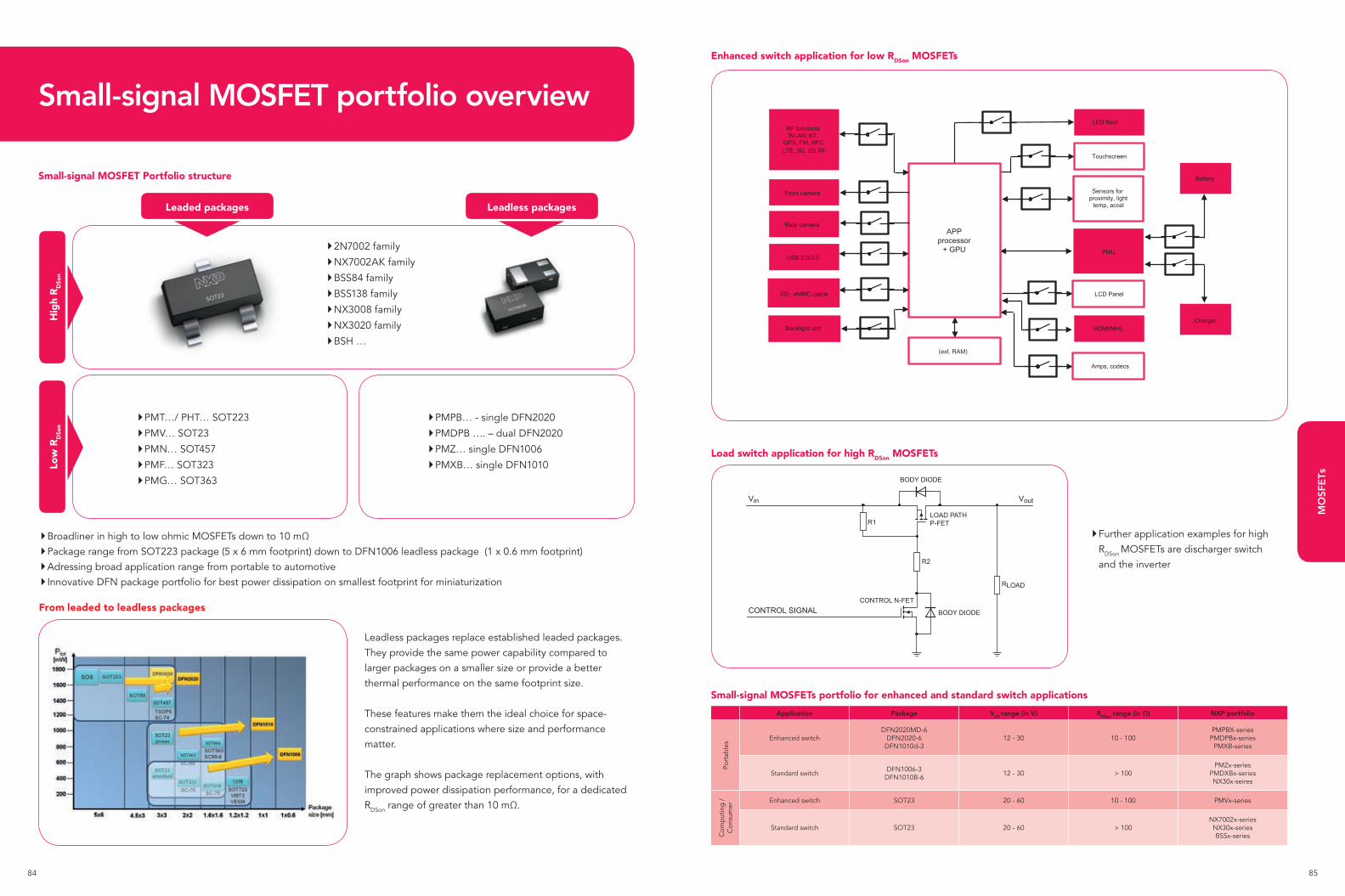
84 85
MO
SFE
Ts
Broadliner in high to low ohmic MOSFETs down to 10 mΩ Package range from SOT223 package (5 x 6 mm footprint) down to DFN1006 leadless package (1 x 0.6 mm footprint) Adressing broad application range from portable to automotive Innovative DFN package portfolio for best power dissipation on smallest footprint for miniaturization
Leadless packages replace established leaded packages. They provide the same power capability compared to larger packages on a smaller size or provide a better thermal performance on the same footprint size.
These features make them the ideal choice for space-constrained applications where size and performance matter.
The graph shows package replacement options, with improved power dissipation performance, for a dedicated RDSon range of greater than 10 mΩ.
Further application examples for high RDSon MOSFETs are discharger switch and the inverter
Small-signal MOSFET portfolio overview
Small-signal MOSFET Portfolio structure
Enhanced switch application for low RDSon MOSFETs
Load switch application for high RDSon MOSFETs
Small-signal MOSFETs portfolio for enhanced and standard switch applications
Touchscreen
APP processor
+ GPU
HDMI/MHL
Rear camera
Front camera
USB 2.0/3.0 PMU
Sensors for proximity, light
temp, accel
(ext. RAM)
SD-, eMMC-cards
Backlight unit
LCD Panel
LED flash RF functions WLAN, BT,
GPS, FM, NFC LTE, 3G, 2G RF
Amps, codecs
Battery
Charger
Vin Vout
CONTROL SIGNAL
RLOAD
BODY DIODE
BODY DIODE
LOAD PATHP-FET
CONTROL N-FET
R2
R1
Leaded packages
Hig
h R
DSo
nLo
w R
DSo
n
Leadless packages
2N7002 family
NX7002AK family
BSS84 family
BSS138 family
NX3008 family
NX3020 family
BSH …
PMT…/ PHT… SOT223
PMV… SOT23
PMN… SOT457
PMF… SOT323
PMG… SOT363
PMPB… - single DFN2020
PMDPB …. – dual DFN2020
PMZ… single DFN1006
PMXB… single DFN1010
From leaded to leadless packages
Application Package VDS range (in V) RDSon range (in Ω) NXP portfolio
Port
able
s Enhanced switchDFN2020MD-6
DFN2020-6 DFN1010d-3
12 - 30 10 - 100 PMPBX-series
PMDPBx-series PMXB-series
Standard switch DFN1006-3 DFN1010B-6 12 - 30 > 100
PMZx-series PMDXBx-series NX30x-seires
Com
put
ing
/
Con
sum
er
Enhanced switch SOT23 20 - 60 10 - 100 PMVx-series
Standard switch SOT23 20 - 60 > 100NX7002x-series
NX30x-series BSSx-series
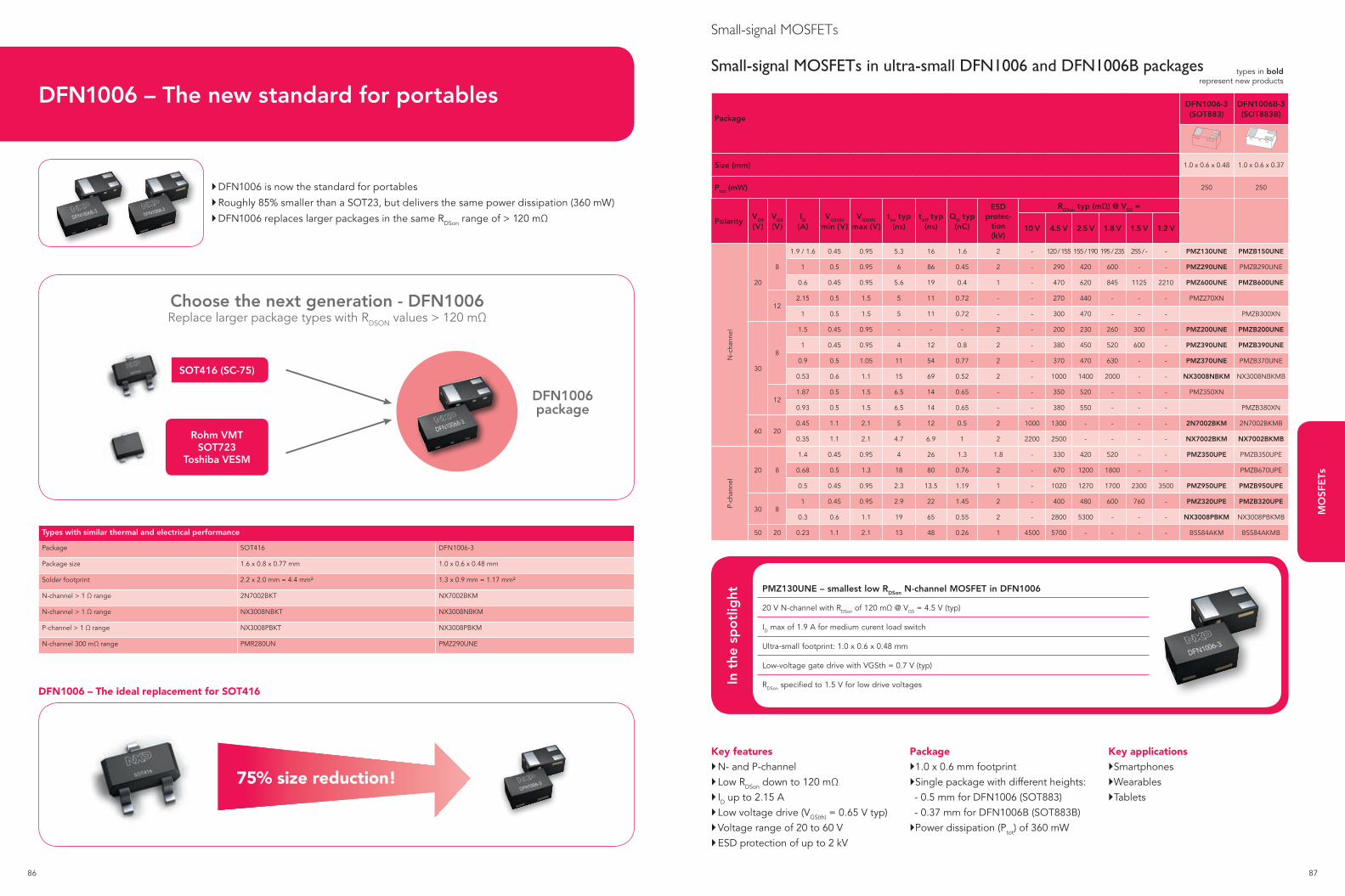
86 87
MO
SFE
Ts
Key features N- and P-channel Low RDSon down to 120 mΩ ID up to 2.15 A Low voltage drive (VGS(th) = 0.65 V typ) Voltage range of 20 to 60 V ESD protection of up to 2 kV
Package1.0 x 0.6 mm footprintSingle package with different heights:- 0.5 mm for DFN1006 (SOT883)- 0.37 mm for DFN1006B (SOT883B)Power dissipation (Ptot) of 360 mW
Key applications Smartphones WearablesTablets
In t
he s
po
tlig
ht PMZ130UNE – smallest low RDSon N-channel MOSFET in DFN1006
20 V N-channel with RDSon of 120 mΩ @ VGS = 4.5 V (typ)
ID max of 1.9 A for medium curent load switch
Ultra-small footprint: 1.0 x 0.6 x 0.48 mm
Low-voltage gate drive with VGSth = 0.7 V (typ)
RDSon specified to 1.5 V for low drive voltages
DFN1006 – The new standard for portables
DFN1006 is now the standard for portables
Roughly 85% smaller than a SOT23, but delivers the same power dissipation (360 mW)
DFN1006 replaces larger packages in the same RDSon range of > 120 mΩ
Small-signal MOSFETs
Small-signal MOSFETs in ultra-small DFN1006 and DFN1006B packages
Package
DFN1006-3 (SOT883)
DFN1006B-3 (SOT883B)
Size (mm) 1.0 x 0.6 x 0.48 1.0 x 0.6 x 0.37
Ptot (mW) 250 250
PolarityVDS (V)
VGS (V)
ID (A)
VGS(th)
min (V)VGS(th)
max (V)ton typ
(ns)toff typ
(ns)QG typ
(nC)
ESD protec-
tion (kV)
RDSon typ (mΩ) @ VGS =
10 V 4.5 V 2.5 V 1.8 V 1.5 V 1.2 V
N-c
hann
el
20
8
1.9 / 1.6 0.45 0.95 5.3 16 1.6 2 - 120 / 155 155 / 190 195 / 235 255 / - - PMZ130UNE PMZB150UNE
1 0.5 0.95 6 86 0.45 2 - 290 420 600 - - PMZ290UNE PMZB290UNE
0.6 0.45 0.95 5.6 19 0.4 1 - 470 620 845 1125 2210 PMZ600UNE PMZB600UNE
122.15 0.5 1.5 5 11 0.72 - - 270 440 - - - PMZ270XN
1 0.5 1.5 5 11 0.72 - - 300 470 - - - PMZB300XN
30
8
1.5 0.45 0.95 - - - 2 - 200 230 260 300 - PMZ200UNE PMZB200UNE
1 0.45 0.95 4 12 0.8 2 - 380 450 520 600 - PMZ390UNE PMZB390UNE
0.9 0.5 1.05 11 54 0.77 2 - 370 470 630 - - PMZ370UNE PMZB370UNE
0.53 0.6 1.1 15 69 0.52 2 - 1000 1400 2000 - - NX3008NBKM NX3008NBKMB
121.87 0.5 1.5 6.5 14 0.65 - - 350 520 - - - PMZ350XN
0.93 0.5 1.5 6.5 14 0.65 - - 380 550 - - - PMZB380XN
60 200.45 1.1 2.1 5 12 0.5 2 1000 1300 - - - - 2N7002BKM 2N7002BKMB
0.35 1.1 2.1 4.7 6.9 1 2 2200 2500 - - - - NX7002BKM NX7002BKMB
P-ch
anne
l
20 8
1.4 0.45 0.95 4 26 1.3 1.8 - 330 420 520 - - PMZ350UPE PMZB350UPE
0.68 0.5 1.3 18 80 0.76 2 - 670 1200 1800 - - PMZB670UPE
0.5 0.45 0.95 2.3 13.5 1.19 1 - 1020 1270 1700 2300 3500 PMZ950UPE PMZB950UPE
30 81 0.45 0.95 2.9 22 1.45 2 - 400 480 600 760 - PMZ320UPE PMZB320UPE
0.3 0.6 1.1 19 65 0.55 2 - 2800 5300 - - - NX3008PBKM NX3008PBKMB
50 20 0.23 1.1 2.1 13 48 0.26 1 4500 5700 - - - - BSS84AKM BSS84AKMB
types in bold represent new products
Types with similar thermal and electrical performance
Package SOT416 DFN1006-3
Package size 1.6 x 0.8 x 0.77 mm 1.0 x 0.6 x 0.48 mm
Solder footprint 2.2 x 2.0 mm = 4.4 mm² 1.3 x 0.9 mm = 1.17 mm²
N-channel > 1 Ω range 2N7002BKT NX7002BKM
N-channel > 1 Ω range NX3008NBKT NX3008NBKM
P-channel > 1 Ω range NX3008PBKT NX3008PBKM
N-channel 300 mΩ range PMR280UN PMZ290UNE
DFN1006 – The ideal replacement for SOT416
75% size reduction!
Choose the next generation - DFN1006Replace larger package types with RDSON values > 120 mΩ
DFN1006package
SOT416 (SC-75)
Rohm VMTSOT723
Toshiba VESM
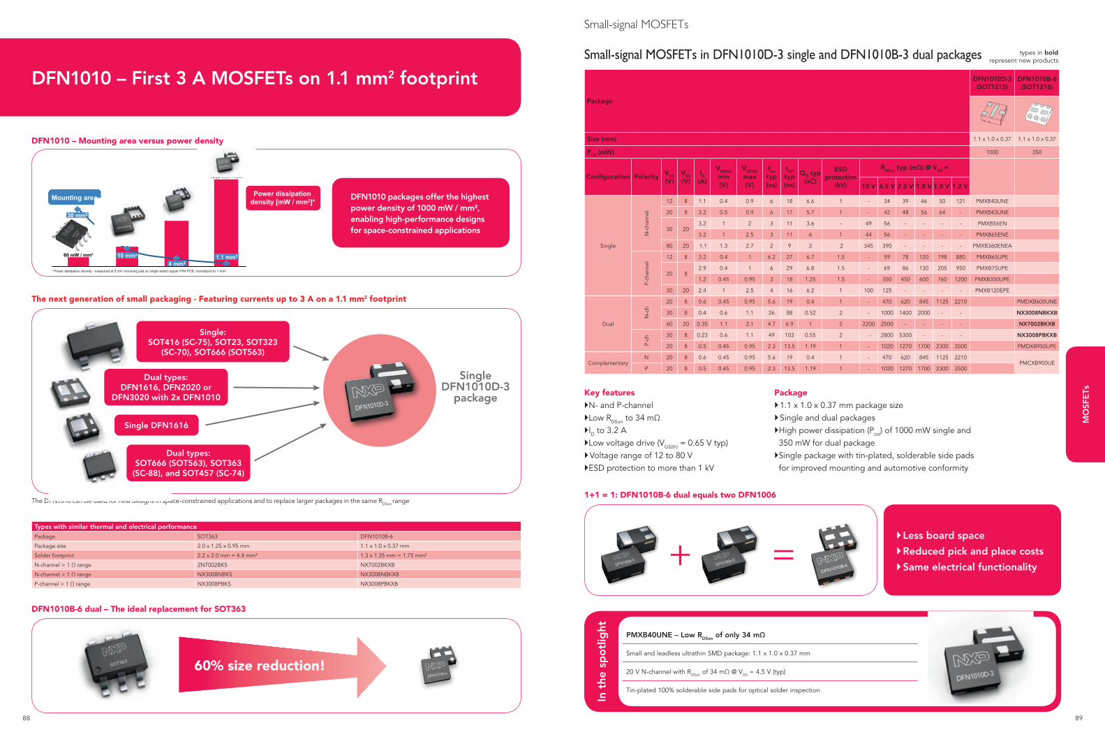
88 89
MO
SFE
TsKey featuresN- and P-channelLow RDSon to 34 mΩID to 3.2 ALow voltage drive (VGS(th) = 0.65 V typ) Voltage range of 12 to 80 VESD protection to more than 1 kV
Package 1.1 x 1.0 x 0.37 mm package size Single and dual packages High power dissipation (Ptot) of 1000 mW single and 350 mW for dual package Single package with tin-plated, solderable side pads for improved mounting and automotive conformity
1+1 = 1: DFN1010B-6 dual equals two DFN1006
In t
he s
po
tlig
ht
PMXB40UNE – Low RDSon of only 34 mΩ
Small and leadless ultrathin SMD package: 1.1 x 1.0 x 0.37 mm
20 V N-channel with RDSon of 34 mΩ @ VGS = 4.5 V (typ)
Tin-plated 100% solderable side pads for optical solder inspection
DFN1010 – First 3 A MOSFETs on 1.1 mm2 footprint
Small-signal MOSFETs
Package
DFN1010D-3(SOT1215)
DFN1010B-6(SOT1216)
Size (mm) 1.1 x 1.0 x 0.37 1.1 x 1.0 x 0.37
Ptot (mW) 1000 350
Configuration Polarity VDS (V)
VGS (V)
ID (A)
VGS(th) min (V)
VGS(th) max (V)
ton typ (ns)
toff typ (ns)
QG typ (nC)
ESD protection
(kV)
RDSon typ (mΩ) @ VGS =
10 V 4.5 V 2.5 V 1.8 V 1.5 V 1.2 V
Single
N-c
hann
el
12 8 1.1 0.4 0.9 6 18 6.6 1 - 34 39 46 50 121 PMXB40UNE
20 8 3.2 0.5 0.9 6 17 5.7 1 - 42 48 56 64 - PMXB43UNE
30 203.2 1 2 3 11 3.6 - 49 56 - - - - PMXB56EN
3.2 1 2.5 3 11 6 1 44 56 - - - - PMXB65ENE
80 20 1.1 1.3 2.7 2 9 3 2 345 390 - - - - PMXB360ENEA
P-ch
anne
l
12 8 3.2 0.4 1 6.2 27 6.7 1.5 - 59 78 120 198 880 PMXB65UPE
20 82.9 0.4 1 6 29 6.8 1.5 - 69 86 130 205 950 PMXB75UPE
1.2 0.45 0.95 3 18 1.25 1.5 - 350 450 600 760 1200 PMXB350UPE
30 20 2.4 1 2.5 4 16 6.2 1 100 125 - - - - PMXB120EPE
Dual
N-c
h
20 8 0.6 0.45 0.95 5.6 19 0.4 1 - 470 620 845 1125 2210 PMDXB600UNE
30 8 0.4 0.6 1.1 26 88 0.52 2 - 1000 1400 2000 - - NX3008NBKXB
60 20 0.35 1.1 2.1 4.7 6.9 1 2 2200 2500 - - - - NX7002BKXB
P-ch
30 8 0.23 0.6 1.1 49 103 0.55 2 - 2800 5300 - - - NX3008PBKXB
20 8 0.5 0.45 0.95 2.3 13.5 1.19 1 - 1020 1270 1700 2300 3500 PMDXB950UPE
ComplementaryN 20 8 0.6 0.45 0.95 5.6 19 0.4 1 - 470 620 845 1125 2210
PMCXB900UE P 20 8 0.5 0.45 0.95 2.3 13.5 1.19 1 - 1020 1270 1700 2300 3500
Small-signal MOSFETs in DFN1010D-3 single and DFN1010B-3 dual packages types in bold represent new products
The next generation of small packaging - Featuring currents up to 3 A on a 1.1 mm2 footprint
The DFN1010 can be used for new designs in space-constrained applications and to replace larger packages in the same RDSon range
SingleDFN1010D-3
package
Single:SOT416 (SC-75), SOT23, SOT323
(SC-70), SOT666 (SOT563)
Dual types:DFN1616, DFN2020 or
DFN3020 with 2x DFN1010
Dual types:SOT666 (SOT563), SOT363
(SC-88), and SOT457 (SC-74)
Single DFN1616
DFN1010 – Mounting area versus power density
Types with similar thermal and electrical performancePackage SOT363 DFN1010B-6
Package size 2.0 x 1.25 x 0.95 mm 1.1 x 1.0 x 0.37 mm
Solder footprint 2.2 x 2.0 mm = 4.4 mm² 1.3 x 1.35 mm = 1.75 mm²
N-channel > 1 Ω range 2N7002BKS NX7002BKXB
N-channel > 1 Ω range NX3008NBKS NX3008NBKXB
P-channel > 1 Ω range NX3008PBKS NX3008PBKXB
DFN1010B-6 dual – The ideal replacement for SOT363
60% size reduction!
* Power dissipation density - measured at 6 cm2 mounting pad on single-sided copper FR4 PCB, normalized to 1 mm2
425 mW / mm
190 mW / mm
60 mW / mm
Mounting area
4 mm2 10 mm2
Power dissipation density [mW / mm2]*
1.1 mm2
1000 mW / mm
30 mm2
DFN1010 packages offer the highest power density of 1000 mW / mm², enabling high-performance designs for space-constrained applications
Less board space
Reduced pick and place costs
Same electrical functionality+ =
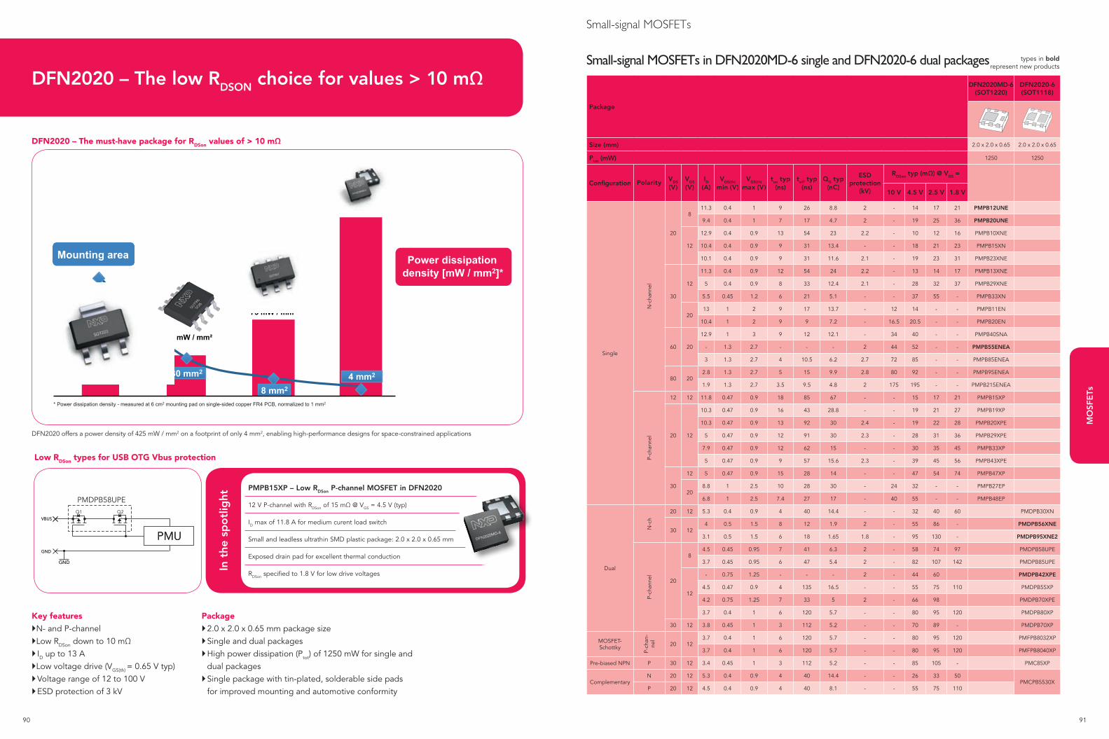
90 91
MO
SFE
Ts
Key featuresN- and P-channelLow RDSon down to 10 mΩ ID up to 13 ALow voltage drive (VGS(th) = 0.65 V typ) Voltage range of 12 to 100 V ESD protection of 3 kV
Package 2.0 x 2.0 x 0.65 mm package size Single and dual packages High power dissipation (Ptot) of 1250 mW for single and
dual packages Single package with tin-plated, solderable side pads
for improved mounting and automotive conformity
Low RDSon types for USB OTG Vbus protection
Q1
PMUPMU
Q2
GNDGND
GNDGND
VBUSVBUS
PMDPB58UPE
In t
he s
po
tlig
ht
PMPB15XP – Low RDSon P-channel MOSFET in DFN2020
12 V P-channel with RDSon of 15 mΩ @ VGS = 4.5 V (typ)
ID max of 11.8 A for medium curent load switch
Small and leadless ultrathin SMD plastic package: 2.0 x 2.0 x 0.65 mm
Exposed drain pad for excellent thermal conduction
RDSon specified to 1.8 V for low drive voltages
Small-signal MOSFETs
Package
DFN2020MD-6 (SOT1220)
DFN2020-6 (SOT1118)
Size (mm) 2.0 x 2.0 x 0.65 2.0 x 2.0 x 0.65
Ptot (mW) 1250 1250
Configuration Polarity VDS (V)
VGS (V)
ID (A)
VGS(th)
min (V)VGS(th)
max (V)ton typ
(ns)toff typ
(ns)QG typ
(nC)
ESD protection
(kV)
RDSon typ (mΩ) @ VGS =
10 V 4.5 V 2.5 V 1.8 V
Single
N-c
hann
el
20
811.3 0.4 1 9 26 8.8 2 - 14 17 21 PMPB12UNE
9.4 0.4 1 7 17 4.7 2 - 19 25 36 PMPB20UNE
12
12.9 0.4 0.9 13 54 23 2.2 - 10 12 16 PMPB10XNE
10.4 0.4 0.9 9 31 13.4 - - 18 21 23 PMPB15XN
10.1 0.4 0.9 9 31 11.6 2.1 - 19 23 31 PMPB23XNE
30
12
11.3 0.4 0.9 12 54 24 2.2 - 13 14 17 PMPB13XNE
5 0.4 0.9 8 33 12.4 2.1 - 28 32 37 PMPB29XNE
5.5 0.45 1.2 6 21 5.1 - - 37 55 - PMPB33XN
2013 1 2 9 17 13.7 - 12 14 - - PMPB11EN
10.4 1 2 9 9 7.2 - 16.5 20.5 - - PMPB20EN
60 20
12.9 1 3 9 12 12.1 - 34 40 - - PMPB40SNA
- 1.3 2.7 - - - 2 44 52 - - PMPB55ENEA
3 1.3 2.7 4 10.5 6.2 2.7 72 85 - - PMPB85ENEA
80 202.8 1.3 2.7 5 15 9.9 2.8 80 92 - - PMPB95ENEA
1.9 1.3 2.7 3.5 9.5 4.8 2 175 195 - - PMPB215ENEA
P-ch
anne
l
12 12 11.8 0.47 0.9 18 85 67 - - 15 17 21 PMPB15XP
20 12
10.3 0.47 0.9 16 43 28.8 - - 19 21 27 PMPB19XP
10.3 0.47 0.9 13 92 30 2.4 - 19 22 28 PMPB20XPE
5 0.47 0.9 12 91 30 2.3 - 28 31 36 PMPB29XPE
7.9 0.47 0.9 12 62 15 - - 30 35 45 PMPB33XP
5 0.47 0.9 9 57 15.6 2.3 - 39 45 56 PMPB43XPE
30
12 5 0.47 0.9 15 28 14 - - 47 54 74 PMPB47XP
208.8 1 2.5 10 28 30 - 24 32 - - PMPB27EP
6.8 1 2.5 7.4 27 17 - 40 55 - - PMPB48EP
Dual
N-c
h
20 12 5.3 0.4 0.9 4 40 14.4 - - 32 40 60 PMDPB30XN
30 124 0.5 1.5 8 12 1.9 2 - 55 86 - PMDPB56XNE
3.1 0.5 1.5 6 18 1.65 1.8 - 95 130 - PMDPB95XNE2
P-ch
anne
l
20
84.5 0.45 0.95 7 41 6.3 2 - 58 74 97 PMDPB58UPE
3.7 0.45 0.95 6 47 5.4 2 - 82 107 142 PMDPB85UPE
12
- 0.75 1.25 - - - 2 - 44 60 PMDPB42XPE
4.5 0.47 0.9 4 135 16.5 - - 55 75 110 PMDPB55XP
4.2 0.75 1.25 7 33 5 2 - 66 98 PMDPB70XPE
3.7 0.4 1 6 120 5.7 - - 80 95 120 PMDPB80XP
30 12 3.8 0.45 1 3 112 5.2 - - 70 89 - PMDPB70XP
MOSFET-Schottky
P-ch
an-
nel
20 123.7 0.4 1 6 120 5.7 - - 80 95 120 PMFPB8032XP
3.7 0.4 1 6 120 5.7 - - 80 95 120 PMFPB8040XP
Pre-biased NPN P 30 12 3.4 0.45 1 3 112 5.2 - - 85 105 - PMC85XP
ComplementaryN 20 12 5.3 0.4 0.9 4 40 14.4 - - 26 33 50
PMCPB5530XP 20 12 4.5 0.4 0.9 4 40 8.1 - - 55 75 110
Small-signal MOSFETs in DFN2020MD-6 single and DFN2020-6 dual packages types in bold represent new products
DFN2020 – The must-have package for RDSon values of > 10 mΩ
* Power dissipation density - measured at 6 cm2 mounting pad on single-sided copper FR4 PCB, normalized to 1 mm2
75 mW / mm
60 mW / mm
40 mW / mm
8 mm2
30 mm2 4 mm2
425 mW / mm
45 mm2
Mounting area Power dissipation density [mW / mm2]*
DFN2020 – The low RDSON choice for values > 10 mΩ
DFN2020 offers a power density of 425 mW / mm2 on a footprint of only 4 mm2, enabling high-performance designs for space-constrained applications
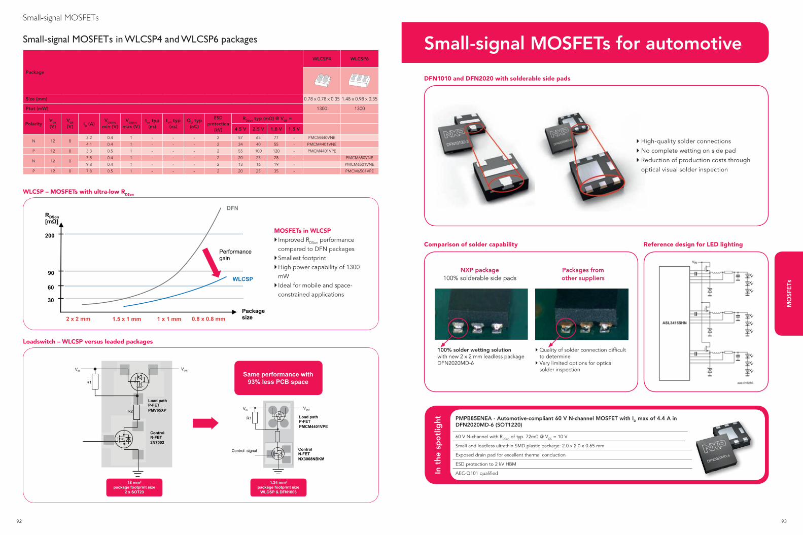
92 93
MO
SFE
Ts
Small-signal MOSFETs
Small-signal MOSFETs in WLCSP4 and WLCSP6 packages
Package
WLCSP4 WLCSP6
Size (mm) 0.78 x 0.78 x 0.35 1.48 x 0.98 x 0.35
Ptot (mW) 1300 1300
PolarityVDS (V)
VGS (V) ID (A)
VGS(th) min (V)
VGS(th) max (V)
ton typ (ns)
toff typ (ns)
QG typ (nC)
ESD protection
(kV)
RDSon typ (mΩ) @ VGS =
4.5 V 2.5 V 1.8 V 1.5 V
N 12 83.2 0.4 1 - - - 2 57 65 77 - PMCM440VNE
4.1 0.4 1 - - - 2 34 40 55 - PMCM4401VNE
P 12 8 3.3 0.5 1 - - - 2 55 100 120 - PMCM4401VPE
N 12 87.8 0.4 1 - - - 2 20 23 28 - PMCM650VNE
9.8 0.4 1 - - - 2 13 16 19 - PMCM6501VNE
P 12 8 7.8 0.5 1 - - - 2 20 25 35 - PMCM6501VPE
WLCSP – MOSFETs with ultra-low RDSon
Loadswitch – WLCSP versus leaded packages
RDSon [m ]
60
30
90 WLCSP
DFN
2 x 2 mm 1.5 x 1 mm 1 x 1 mm 0.8 x 0.8 mm
200
Package size
Performance gain
Vin
R1
R2
Vout
Control N-FET 2N7002
Load path P-FET PMV65XP Vin
R1
R2
Vout
Control signal
Load path P-FET PMCM4401VPE
Control N-FET NX3008NBKM
Same performance with 93% less PCB space
1.24 mm² package footprint size
WLCSP & DFN1006
18 mm²package footprint size
2 x SOT23
MOSFETs in WLCSP Improved RDSon performance
compared to DFN packages Smallest footprint High power capability of 1300
mW Ideal for mobile and space-
constrained applications
Small-signal MOSFETs for automotive
DFN1010 and DFN2020 with solderable side pads
Comparison of solder capability Reference design for LED lighting
NXP package100% solderable side pads
100% solder wetting solution with new 2 x 2 mm leadless package DFN2020MD-6
Quality of solder connection difficult to determine
Very limited options for optical solder inspection
Packages from other suppliers
In t
he s
po
tlig
ht PMPB85ENEA - Automotive-compliant 60 V N-channel MOSFET with ID max of 4.4 A in DFN2020MD-6 (SOT1220)
60 V N-channel with RDSon of typ. 72mΩ @ VGS = 10 V
Small and leadless ultrathin SMD plastic package: 2.0 x 2.0 x 0.65 mm
Exposed drain pad for excellent thermal conduction
ESD protection to 2 kV HBM
AEC-Q101 qualified
High-quality solder connections
No complete wetting on side pad
Reduction of production costs through
optical visual solder inspection
94 95
MO
SFE
Ts
Automotive MOSFETs
types in bold represent new products
Automotive MOSFETs
Automotive-compliant small-signal MOSFETs
Package
SOT223SOT457 (SC-74)
SOT23SOT363 (SC-88)
SOT323 (SC-70)
SOT666DFN2020MD-6
(SOT1220)DFN1010D-3
(SOT1215)DFN1006 (SOT883)
Size (mm) 6.5 x 3.5 x 1.65 2.9 x 1.5 x 1.0 2.9 x 1.3 x 1.0 2.0 x 1.25 x 0.95 2.0 x 1.25 x 0.95 1.6 x 1.2 x 0.55 2.0 x 2.0 x 0.65 1.1 x 1.0 x 0.37 1.0 x 0.6 x 0.5
Ptot (mW) 1700 600 250 300 200 300 1250 1000 250
Polarity Configuration VDS (V) VGS (V) ID (A)VGS(th)
min (V)VGS(th)
max (V)ton typ
(ns)toff typ
(ns)QG typ
(nC)
ESD protection
(kV)
RDSon typ (mΩ) @ VGS =
10 V 4.5 V 2.5 V 1.8 V
N-c
hann
el
Single
208 5.2 0.5 1.5 12 128 6.4 2 - 24 28 72 PMV28UNEA
12 5.9 0.75 1.25 16 49 31 2 - 14 20 - PMV20XNEA
30
8 0.4 0.6 1.1 26 88 0.52 2 - 1000 1400 2000 NX3008NBK NX3008NBKW
20
4.9 1 2.5 9.9 29 20 2.8 15 21 - - PMV25ENEA
3.7 1 2.5 - - - 1.6 - - - - PMV50ENEA
1.9 1 2.5 5.4 12 5.4 1.6 54 74 - - PMV100ENEA
40 20 2.5 1 2.5 14 14 2.4 1 95 120 - - PMV130ENEA
60 20
12.9 1 3 9 12 12.1 - 34 40 - - PMPB40SNA
- 1.3 2.7 - - - 2 44 52 - - PMPB55ENEA
2.8 1 2.5 9 33 19 2.8 46 52 - - PMV55ENEA
3 1.3 2.7 4 10.5 6.2 2.7 72 85 - - PMPB85ENEA
1.9 1 2.5 - - - 2 - - - - PMV120ENEA
1.4 1 2.5 - - - 2 - - - - PMV230ENEA
0.7 1 2.5 - - - 2.5 - - - - PMV450ENEA
0.36 0.9 1.5 5 13 0.72 - 900 1000 - - BSS138P BSS138PW
0.36 0.48 1.6 10 58 0.6 1.5 1000 1100 1400 - BSS138BK BSS138BKW
0.3 1 2.5 11 19 0.5 2 1000 1300 - - 2N7002BK 2N7002BKW 2N7002BKM
0.3 1 2.5 16 60 1.09 3 1100 1300 - - 2N7002CK
0.2 0.8 1.5 5 36 0.39 Yes 2700 3000 4000 - BSS138AKA
80 20
1.9 1.3 2.7 3.5 9.5 4.8 2 175 195 - - PMPB215ENEA
2.8 1.3 2.7 5 15 9.9 2.8 80 92 - - PMPB95ENEA
1.1 1.3 2.7 2 9 3 2 345 390 - - PMXB360ENEA
100 20- 1.3 2.7 - - - 2 275 300 - - PMT280ENEA
- 1.3 2.7 - - - 2 520 560 - - PMT560ENEA
Dual
20 8 0.8 0.5 0.95 10 117 0.45 2 - 380 620 1100 PMDT290UNE
30 8 0.4 0.6 1.1 26 88 0.52 2 - 1000 1400 2000 NX3008NBKS NX3008NBKV
60 20
0.3 1 2.5 11 19 0.5 2 1000 1300 - - 2N7002BKS
0.36 0.48 1.6 10 58 0.6 1.5 1000 1100 1400 - BSS138BKS
0.36 0.9 1.5 5 13 0.72 - 900 1000 - - BSS138PS
P-ch
anne
l Single
20
86 0.45 0.95 8 50 15.6 4 - 37 45 59 PMN40UPEA
2 0.5 1.1 7 50 6 - - 100 155 210 NX2301P
12
5.7 0.75 1.25 15 37 15 2 - 27 39 - PMN27XPEA
5.7 0.75 1.25 17 33 11.5 2 - 41 56 - PMN42XPEA
4.4 0.75 1.25 - - - 2 - 26 - - PMV30XPEA
3.5 0.75 1.25 11 61 8.5 - - 48 71 - PMV48XPA
4.1 0.75 1.25 15 51 8.7 - - 48 72 - PMN48XPA
3.3 0.75 1.25 7 36 5 2 - 67 99 - PMV65XPEA
4.1 0.75 1.25 7 40 5.2 2 - 70 101 - PMN70XPEA
2.2 0.75 1.25 - - - 2 - 93 - - PMV100XPEA
308 0.23 0.6 1.1 49 103 0.55 2 - 2800 5300 - NX3008PBK NX3008PBKW
20 4 1 3 6 38 18 3 23 39 - - PMV50EPEA
40 20 1.5 1 2.5 4 26 4.7 1 180 220 - - PMV250EPEA
50 20 0.2 1.1 2.1 24 73 0.26 1 5300 6000 - - BSS84AK BSS84AKW BSS84AKM
60 202.2 1 3 - - - 2 99 110 - - PMV100EPEA
0.9 1 3 - - - 2 217 241 - - PMV240EPEA
70 20 2.3 1 3 - - - 2 156 177 - - PMT200EPEA
Dual
20 8 0.55 0.5 1.3 48 152 0.76 2 - 670 1200 1800 PMDT670UPE
30 8 0.2 0.6 1.1 49 103 0.55 2 - 2800 5300 - NX3008PBKS NX3008PBKV
50 20 0.16 1.1 2.1 24 73 0.26 1 5300 6000 - - BSS84AKS BSS84AKV
NCompl
20 8 0.73 0.5 0.95 10 117 0.45 2 - 290 420 600PMGD290UCEA
P 20 8 0.5 0.5 1.3 48 152 0.76 2 - 670 1200 1800
96 97
MO
SFE
Ts
Small-signal MOSFETsSmall-signal MOSFETs
Package
SOT223 SOT89 SOT23SOT323 (SC-70)
DFN1006-3 (SOT883)
DFN1006B-3 (SOT883B)
Size (mm) 6.5 x 3.5 x 1.65 4.5 x 2.5 x 1.5 2.9 x 1.3 x 1.0 2.0 x 1.25 x 0.95 1.0 x 0.6 x 0.48 1.0 x 0.6 x 0.37
Ptot (mW) 1700 600 250 200 250 250
VDS (V) VGS (V) ID (A)VGS(th)
min (V)VGS(th)
max (V) ton typ (ns) toff typ (ns) QG typ (nC)ESD
protection (kV)
RDSon typ (mΩ) @ VGS =
10 V 4.5 V 2.5 V 1.8 V
20
8
5.2 0.5 1.5 12 128 6.4 2 - 24 28 72 PMV28UNEA1.9 0.4 1 8 31 2.2 2 - 63 77 114 PMF63UNE2.2 0.4 1 6 21 2.6 2 - 64 78 110 PMV65UNE
1.05 0.4 - 2 45 3.9 - 140 180 240 BSH1051.9 / 1.6 0.45 0.95 5.3 16 1.6 2 - 120 / 155 155 / 190 195 / 235 PMZ130UNE PMZB150UNE
1 0.5 0.95 6 86 0.45 2 - 290 420 600 PMZ290UNE PMZB290UNE0.6 0.45 0.95 5.6 19 0.4 1 - 470 620 845 PMZ600UNE PMZB600UNE
12
5.9 0.75 1.25 16 49 31 2 - 14 20 - PMV20XNEA8.6 0.47 0.9 7 135 7.7 - 15 18 22 PMV16XN4.8 0.5 1.5 12 128 6.4 2 - 19 26 - PMV20XNE5.4 0.4 0.9 7 35 6.2 - 24 30 40 PMV30UN23.2 0.5 1.5 11 93 4.9 2 - 28 39 - PMV30XNE
2.15 0.5 1.5 16 17 0.72 - - 270 440 - PMZ270XN PMZB300XN
30
8
1.5 0.45 0.95 - - - 2 - 200 230 260 PMZ200UNE PMZB200UNE1 0.45 0.95 4 12 0.8 2 - 380 450 520 PMZ390UNE PMZB390UNE
0.9 0.5 1.05 20 81 0.77 2 - 370 470 630 PMZ370UNE PMZB370UNE0.85 0.4 - 6 27 - - 400 - 600 BSH1030.4 0.6 1.1 26 88 0.52 2 - 1000 1400 2000 NX3008NBK NX3008NBKW NX3008NBKM NX3008NBKMB
124.4 0.4 0.9 9 34 7 - - 36 43 56 PMV40UN20.9 0.5 1.5 8 11 0.74 2 - 234 324 - PMF250XNE
1.87 0.5 1.5 16 19.5 0.65 - - 350 520 - PMZ350XN PMZB380XN
20
7.6 1 2 9 9 7.2 - 17 21 - - PMV20EN4.9 1 2.5 9.9 29 20 2.8 15 21 - - PMV25ENEA3.7 1 2.5 - - - 1.6 - - - - PMV50ENEA10 1 2.8 18 44 24 - 20 30 - - BSP0303.1 1 2.5 18 78 6.5 - 28 37 - - PMV37EN25.1 1 2 3 11 3.6 - 35 43 - - PMV45EN22.1 1 2.5 3 15 2.6 2 70 90 - - PMV90ENE6 1 2.8 14 36 - - 80 120 - - BSP100
1.9 1 2 3 15 6.4 - 77 102 - - BSH1080.18 0.8 1.5 10 51 0.34 - 2700 3000 4000 - NX3020NAK NX3020NAKW
40 20 2.5 1 2.5 14 14 2.4 1 95 120 - - PMV130ENEA50 20 0.1 0.4 1.8 2 5 2 2800 3800 - - BSN20BK
558 0.3 0.4 1.3 4 11 1 - - 2300 2400 3100 BSH121
10 0.3 0.4 1.3 4 11 1 3 - 2300 2400 3100 BSH111BK
60 20
2.8 1 2.5 9 33 19 2.8 46 52 - PMV55ENEA1.9 1 2.5 - - - 2 - - - - PMV120ENEA1.4 1 2.5 - - - 2 - - - - PMV230ENEA0.7 1 2.5 - - - 2.5 - - - - PMV450ENEA0.36 0.9 1.5 5 13 0.72 - 900 1000 - BSS138P BSS138PW0.36 0.48 1.6 10 58 0.6 1.5 1000 1100 1400 - BSS138BK BSS138BKW0.3 1 2.5 11 19 0.5 2 1000 1300 - - 2N7002BKM 2N7002BKMB
0.19 1.1 2.1 12 34 0.33 Yes 3000 3700 - - NX7002AK NX7002AKW0.27 1.1 2.1 4.7 6.9 1 2 2200 2500 - - NX7002BK NX7002BKW NX7002BKM NX7002BKMB
10020
3 2 4 - - - - 57 - - - PHT6NQ10T3.5 2 4 - - - - 200 - - - PHT4NQ10T- 1.3 2.7 - - - 2 275 300 - - PMT280ENEA- 1.3 2.7 - - - 2 520 560 - - PMT560ENEA
0.85 2 4 19 13 4.6 - 400 - - - BSH1140.15 1 2.8 3 12 - - 3500 - - - BSS1230.19 1 - 3 12 - - - 5000 - - BST820.52 1 - 3 12 - - - 5000 - - BSP110
30 1.9 2 4 10.5 12.5 7 - 213 - - - PMV213SN
200 200.4 0.8 2.8 6 49 - - 1600 - - - BSS87
0.55 0.4 2 10 45 - - 1700 - 3000 - BSP122240 20 0.375 0.8 2 6 47 - - 2800 - 7500 - BSP89250 20 0.35 0.8 2 6 47 - - 2800 - - BSP126300 20 0.35 0.8 2 6 46 - - 3700 - 4800 - BSP130
M3D109
types in bold represent new productsSmall-signal MOSFETs single (N-channel)
In t
he s
po
tlig
ht
NX7002BKx – NX7002 ESD-protected 60 V N-channel MOSFET series in several SMD packages
ESD protection to 2 kV HBM
Available in single and dual con-figurations
Single packages from SOT23 to DFN1006
Dual packages from SOT363 to DFN1010
98 99
MO
SFE
Ts
In t
he s
po
tlig
ht PMV75UP – 20 V, 77 mΩ P-channel MOSFET
Cross of Si2301 types
Low-voltage gate drive with VGSth = 0.68 V (typ)
Industry-standard SOT23 package
RDSon specified to 1.8 V for low drive voltages
Small-signal MOSFETs
1) SOT23 with enhanced thermal performance
Small-signal MOSFETs
Small-signal MOSFET– Schottky combination
Package
DFN2020-6
Size (mm) 2.0 x 2.0 x 0.65
Ptot (mW) 1250
Configuration VDS (V)
VGS (V)
ID (A)
VGS(th) min (V)
VGS(th) max (V)
ton typ (ns)
toff typ (ns)
QG typ (nC)
IF (A) VR (V) VF typ. (mV)
RDSon typ (mΩ) @ VGS =
4.5 V 2.5 V 1.8 V
Single + Schottky 20 83.7 0.4 1 20 170 5.7 2 30 455 80 95 120 PMFPB8040XP
3.7 0.4 1 20 170 5.7 2.2 30 325 80 95 120 PMFPB8032XP
Package
SOT223 SOT89(SC-62)
SOT457(SC-74)
SOT23 SOT363 (SC-88)
SOT323(SC-70)
DFN1006-3(SOT883)
DFN1006B-3(SOT883B)
Size (mm) 6.5 x 3.5 x 1.65 4.5 x 2.5 x 1.5 2.9 x 1.5 x 1.0 2.9 x 1.3 x 1.0 2.0 x 1.25 x 0.95 2.0 x 1.25 x 0.95 1.0 x 0.6 x 0.48 1.0 x 0.6 x 0.37
Ptot (mW) 1700 1300 600 250 300 200 250 250
VDS (V) VGS (V) ID (A)VGS(th)
min (V)VGS(th)
max (V) ton typ (ns) toff typ (ns) QG typ (nC)ESD
protection(kV)
RDSon typ (mΩ) @ VGS =
10 V 4.5 V 2.5 V 1.8 V
20
8
5.7 0.45 0.95 39 122 21 - - 27 36 57 PMN27UP 5.6 0.45 0.95 11 83 14.7 2 - 27 38 50 PMV27UPE5.3 0.45 0.95 41 122 14.7 2 - 30 38 51 PMV33UPE5.4 0.45 0.95 34 128 15.5 - - 34 42 57 PMN34UP PMV32UP 6 0.45 0.95 29 84 15.6 4 - 37 45 59 PMN40UPE4 0.47 0.9 - - 10.5 3 - 50 57 70 PMN50UPE PMV50UPE2 0.5 1.1 7 50 6 - - 100 - - NX2301P
1.2 0.45 0.95 33 52 3.3 - - 170 210 280 PMV160UP 0.75 0.4 - 6.5 65 - - - 180 - 420 BSH205G2
1.4 0.45 0.95 9 35 1.3 1.8 - 330 420 520 PMZ350UPE PMZB350UPE0.48 0.5 1.3 48 152 0.76 2 - 670 1200 1800 PMZB670UPE 0.5 0.45 0.95 2.3 13.5 1.19 1 - 1020 1270 1700 PMZ950UPE PMZB950UPE
12
4.4 0.75 1.25 - - - 2 - 26 - - PMV30XPEA
5.7 0.75 1.25 37 66 15 2 - 27 39 - PMN27XPE5.7 0.75 1.25 44 60 11.5 2 - 41 56 - PMN42XPE
4.1 / 3.5 0.75 1.25 24 84 8.5 - - 48 71 - PMN48XP PMV48XP 4.4 0.47 0.9 7 135 7.7 - - 48 60 82 PMV50XP
3.9 0.55 0.95 28 101 7.6 - - 65 90 - PMV65XP 3.3 0.75 1.25 7 36 5 2 - 67 99 - PMV65XPE
4.1 0.75 1.25 20 57 5.2 2 - 70 101 - PMN70XPE3.2 0.47 0.9 6 120 5 - - 77 95 120 PMV75UP
3.2 0.45 1 20 170 5 - - 80 95 120 PMN80XP 2 0.65 1.15 48 64 4.8 - - 90 125 - PMG85XP
2.2 0.75 1.25 - - - 2 - 93 - - PMV100XPEA 1 0.65 1.15 26 44 2.6 - - 175 240 - PMF170XP
30
81 0.45 0.95 2.9 22 1.45 2 - 400 480 600 PMZ320UPE PMZB320UPE
0.47 0.4 - 6.5 65 - - - 660 - 1100 BSH2030.23 0.6 1.1 49 103 0.55 2 - 2800 5300 - NX3008PBK NX3008PBKW NX3008PBKM NX3008PBKMB
204 1 3 6 38 18 3 23 39 - - PMV50EPEA
3 1 2.8 20 50 - - 220 330 - - BSP250 0.52 1 - 6.5 65 - - 630 890 - - BSH202
40 20 1.8 1 2.5 10 40 4.7 1 180 220 - - PMV250EPEA50 20 0.2 1.1 2.1 24 73 0.26 1 5300 6000 - - BSS84AK BSS84AKW BSS84AKM BSS84AKMB
60 202.2 1 3 - - - 2 99 110 - - PMV100EPEA0.9 1 3 - - - 2 217 241 - - PMV240EPEA
0.3 1 - 6.5 65 - - 2100 - 2700 - BSH201 70 20 2.3 1 3 - - - 2 156 177 - - PMT200EPEA
200 20 0.225 0.8 2.8 5 20 - - 10000 - - - BSP220 240 20 0.2 0.8 2.8 5 20 - - 10000 - - - BSS192 250 20 0.225 0.8 2.8 5 10 - - 10000 - - - BSP225 300 20 0.21 1.95 2.8 5 15 - - 17000 - - - BSP230
M3D109
types in bold represent new productsSmall-signal MOSFETs single (P-channel)
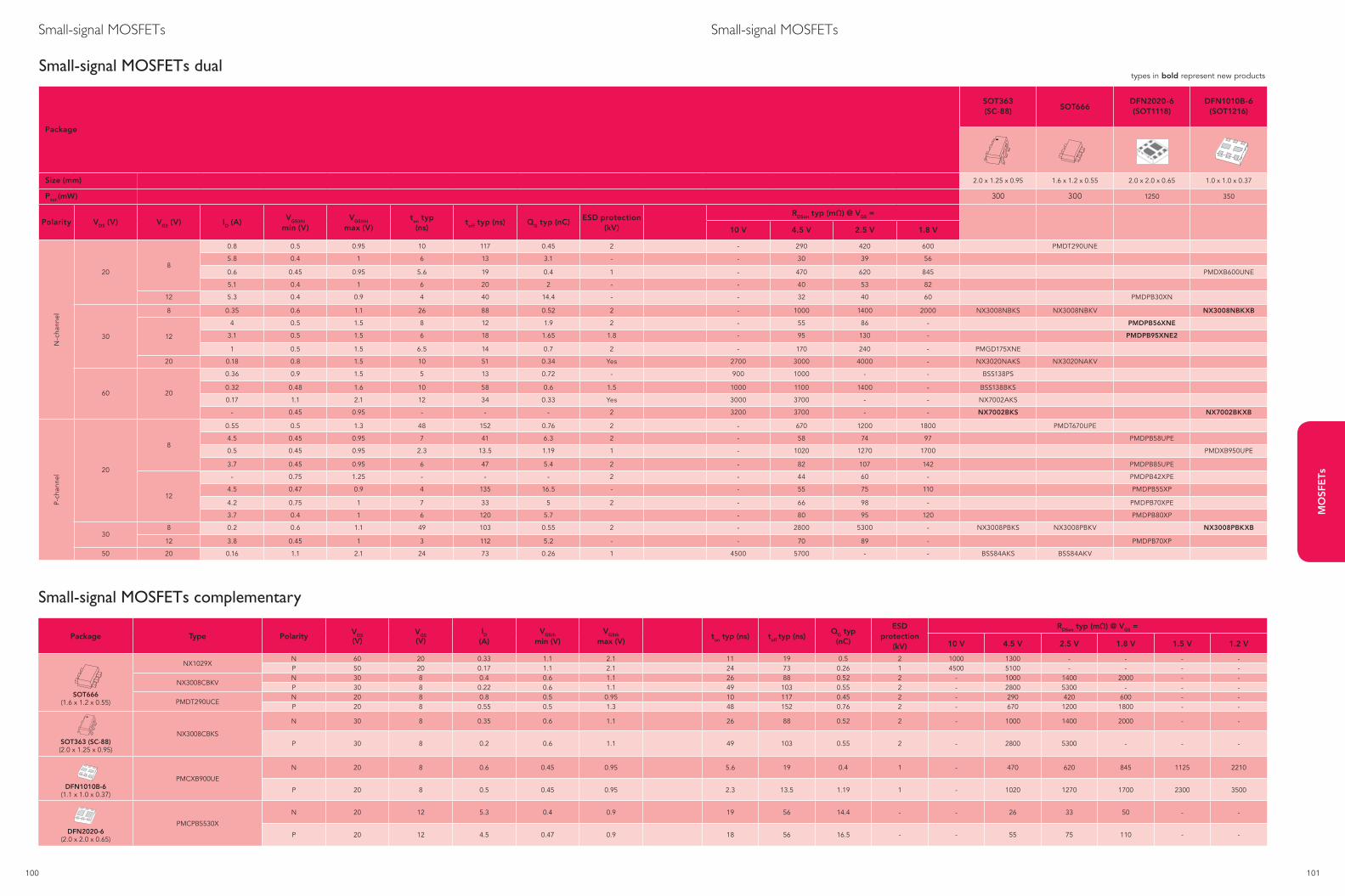
100 101
MO
SFE
Ts
Small-signal MOSFETsSmall-signal MOSFETs
Package
SOT363(SC-88) SOT666
DFN2020-6(SOT1118)
DFN1010B-6(SOT1216)
Siz e (mm) 2.0 x 1.25 x 0.95 1.6 x 1.2 x 0.55 2.0 x 2.0 x 0.65 1.0 x 1.0 x 0.37
Ptot (mW) 300 300 1250 350
Polarity VDS (V) VGS (V) ID (A) VGS(th) min (V)
VGS(th)
max (V)ton typ
(ns)toff typ (ns) QG typ (nC) ESD protection
(kV)
RDSon typ (mΩ) @ VGS =
10 V 4.5 V 2.5 V 1.8 V
N-c
hann
el
208
0.8 0.5 0.95 10 117 0.45 2 - 290 420 600 PMDT290UNE
5.8 0.4 1 6 13 3.1 - - 30 39 56
0.6 0.45 0.95 5.6 19 0.4 1 - 470 620 845 PMDXB600UNE
5.1 0.4 1 6 20 2 - - 40 53 82
12 5.3 0.4 0.9 4 40 14.4 - - 32 40 60 PMDPB30XN
30
8 0.35 0.6 1.1 26 88 0.52 2 - 1000 1400 2000 NX3008NBKS NX3008NBKV NX3008NBKXB
12
4 0.5 1.5 8 12 1.9 2 - 55 86 - PMDPB56XNE
3.1 0.5 1.5 6 18 1.65 1.8 - 95 130 - PMDPB95XNE2
1 0.5 1.5 6.5 14 0.7 2 - 170 240 - PMGD175XNE
20 0.18 0.8 1.5 10 51 0.34 Yes 2700 3000 4000 - NX3020NAKS NX3020NAKV
60 20
0.36 0.9 1.5 5 13 0.72 - 900 1000 - - BSS138PS
0.32 0.48 1.6 10 58 0.6 1.5 1000 1100 1400 - BSS138BKS
0.17 1.1 2.1 12 34 0.33 Yes 3000 3700 - - NX7002AKS
- 0.45 0.95 - - - 2 3200 3700 - - NX7002BKS NX7002BKXB
P-ch
anne
l 20
8
0.55 0.5 1.3 48 152 0.76 2 - 670 1200 1800 PMDT670UPE
4.5 0.45 0.95 7 41 6.3 2 - 58 74 97 PMDPB58UPE
0.5 0.45 0.95 2.3 13.5 1.19 1 - 1020 1270 1700 PMDXB950UPE
3.7 0.45 0.95 6 47 5.4 2 - 82 107 142 PMDPB85UPE
12
- 0.75 1.25 - - - 2 - 44 60 - PMDPB42XPE
4.5 0.47 0.9 4 135 16.5 - - 55 75 110 PMDPB55XP
4.2 0.75 1 7 33 5 2 - 66 98 - PMDPB70XPE
3.7 0.4 1 6 120 5.7 - 80 95 120 PMDPB80XP
308 0.2 0.6 1.1 49 103 0.55 2 - 2800 5300 - NX3008PBKS NX3008PBKV NX3008PBKXB
12 3.8 0.45 1 3 112 5.2 - - 70 89 - PMDPB70XP
50 20 0.16 1.1 2.1 24 73 0.26 1 4500 5700 - - BSS84AKS BSS84AKV
types in bold represent new productsSmall-signal MOSFETs dual
Small-signal MOSFETs complementary
Package Type Polarity VDS (V)
VGS (V)
ID (A)
VGSth min (V)
VGSth max (V)
ton typ (ns) toff typ (ns)QG typ
(nC)
ESDprotection
(kV)
RDSon typ (mΩ) @ VGS =
10 V 4.5 V 2.5 V 1.8 V 1.5 V 1.2 V
SOT666 (1.6 x 1.2 x 0.55)
NX1029XN 60 20 0.33 1.1 2.1 11 19 0.5 2 1000 1300 - - - -P 50 20 0.17 1.1 2.1 24 73 0.26 1 4500 5100 - - - -
NX3008CBKVN 30 8 0.4 0.6 1.1 26 88 0.52 2 - 1000 1400 2000 - -P 30 8 0.22 0.6 1.1 49 103 0.55 2 - 2800 5300 - - -
PMDT290UCEN 20 8 0.8 0.5 0.95 10 117 0.45 2 - 290 420 600 - -P 20 8 0.55 0.5 1.3 48 152 0.76 2 - 670 1200 1800 - -
SOT363 (SC-88) (2.0 x 1.25 x 0.95)
NX3008CBKS
N 30 8 0.35 0.6 1.1 26 88 0.52 2 - 1000 1400 2000 - -
P 30 8 0.2 0.6 1.1 49 103 0.55 2 - 2800 5300 - - -
DFN1010B-6 (1.1 x 1.0 x 0.37)
PMCXB900UE
N 20 8 0.6 0.45 0.95 5.6 19 0.4 1 - 470 620 845 1125 2210
P 20 8 0.5 0.45 0.95 2.3 13.5 1.19 1 - 1020 1270 1700 2300 3500
DFN2020-6 (2.0 x 2.0 x 0.65)
PMCPB5530X
N 20 12 5.3 0.4 0.9 19 56 14.4 - - 26 33 50 - -
P 20 12 4.5 0.47 0.9 18 56 16.5 - - 55 75 110 - -
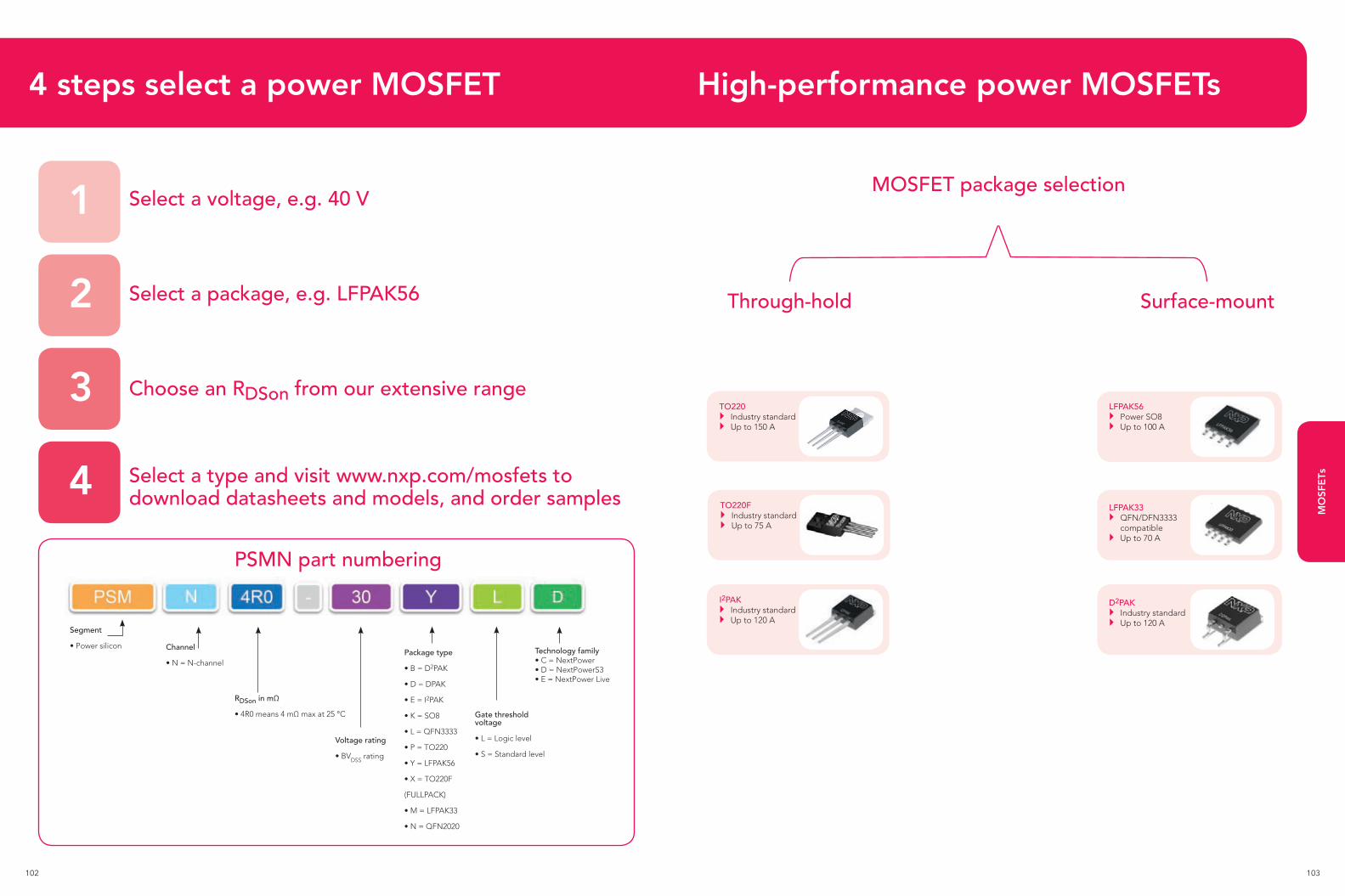
102 103
MO
SFE
Ts
4 steps select a power MOSFET
1
2
3
4
Select a voltage, e.g. 40 V
Select a package, e.g. LFPAK56
Choose an RDSon from our extensive range
Select a type and visit www.nxp.com/mosfets to download datasheets and models, and order samples
PSMN part numbering
Segment
• Power silicon Max Channel
• N = N- channel
RDSon in mΩ
• 4R0 means 4 mΩ max at 25 °C
Voltage rating
• BVDSS
rating
Package type
• B = D2PAK
• D = DPAK
• E = I2PAK
• K = SO8
• L = QFN3333
• P = TO220
• Y = LFPAK56
• X = TO220F
(FULLPACK)
• M = LFPAK33
• N = QFN2020
Gate thresholdvoltage
• L = Logic level
• S = Standard level
Technology family• C = NextPower• D = NextPowerS3 • E = NextPower Live
D2PAK Industry standard Up to 120 A
LFPAK56 Power SO8 Up to 100 A
LFPAK33 QFN/DFN3333 compatible Up to 70 A
TO220 Industry standard Up to 150 A
High-performance power MOSFETs
MOSFET package selection
Through-hold Surface-mount
TO220F Industry standard Up to 75 A
I2PAK Industry standard Up to 120 A
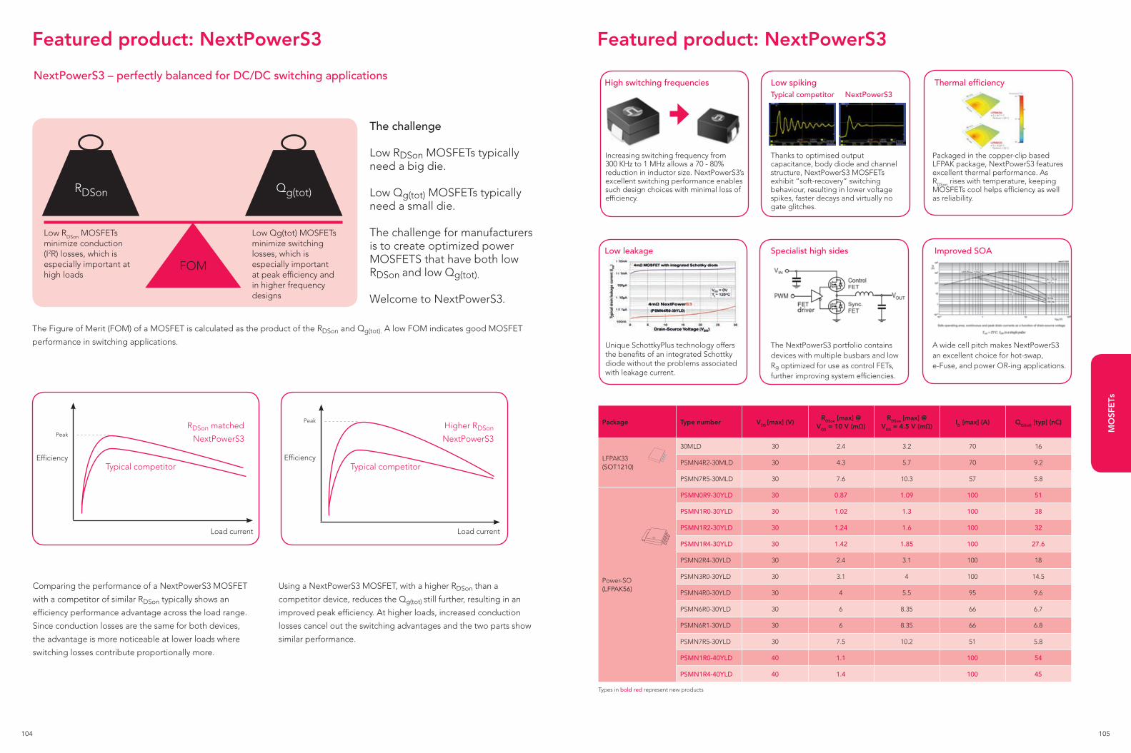
104 105
MO
SFE
Ts
Package Type number VDS [max] (V)RDSon [max] @
VGS = 10 V (mΩ)RDSon [max] @
VGS = 4.5 V (mΩ)ID [max] (A) QG(tot) [typ] (nC)
LFPAK33(SOT1210)
30MLD 30 2.4 3.2 70 16
PSMN4R2-30MLD 30 4.3 5.7 70 9.2
PSMN7R5-30MLD 30 7.6 10.3 57 5.8
Power-SO(LFPAK56)
PSMN0R9-30YLD 30 0.87 1.09 100 51
PSMN1R0-30YLD 30 1.02 1.3 100 38
PSMN1R2-30YLD 30 1.24 1.6 100 32
PSMN1R4-30YLD 30 1.42 1.85 100 27.6
PSMN2R4-30YLD 30 2.4 3.1 100 18
PSMN3R0-30YLD 30 3.1 4 100 14.5
PSMN4R0-30YLD 30 4 5.5 95 9.6
PSMN6R0-30YLD 30 6 8.35 66 6.7
PSMN6R1-30YLD 30 6 8.35 66 6.8
PSMN7R5-30YLD 30 7.5 10.2 51 5.8
PSMN1R0-40YLD 40 1.1 100 54
PSMN1R4-40YLD 40 1.4 100 45
NextPowerS3 – perfectly balanced for DC/DC switching applications
Featured product: NextPowerS3
Comparing the performance of a NextPowerS3 MOSFET
with a competitor of similar RDSon typically shows an
efficiency performance advantage across the load range.
Since conduction losses are the same for both devices,
the advantage is more noticeable at lower loads where
switching losses contribute proportionally more.
Using a NextPowerS3 MOSFET, with a higher RDSon than a
competitor device, reduces the Qg(tot) still further, resulting in an
improved peak efficiency. At higher loads, increased conduction
losses cancel out the switching advantages and the two parts show
similar performance.
Peak
Peak
Efficiency Efficiency
Load current Load current
RDSon matched
NextPowerS3
Higher RDSon
NextPowerS3
Typical competitor Typical competitor
The challenge
Low RDSon MOSFETs typically need a big die.
Low Qg(tot) MOSFETs typically need a small die.
The challenge for manufacturers is to create optimized power MOSFETS that have both low RDSon and low Qg(tot). Welcome to NextPowerS3.
The Figure of Merit (FOM) of a MOSFET is calculated as the product of the RDSon and Qg(tot). A low FOM indicates good MOSFET
performance in switching applications.
Low RDSon MOSFETs minimize conduction (I2R) losses, which is especially important at high loads
Low Qg(tot) MOSFETs minimize switching losses, which is especially important at peak efficiency and in higher frequency designs
High switching frequencies Low spiking Thermal efficiency
Low leakage Specialist high sides Improved SOA
Increasing switching frequency from300 KHz to 1 MHz allows a 70 - 80%reduction in inductor size. NextPowerS3’sexcellent switching performance enablessuch design choices with minimal loss ofefficiency.
Thanks to optimised outputcapacitance, body diode and channelstructure, NextPowerS3 MOSFETsexhibit “soft-recovery” switchingbehaviour, resulting in lower voltagespikes, faster decays and virtually nogate glitches.
Packaged in the copper-clip basedLFPAK package, NextPowerS3 featuresexcellent thermal performance. AsRDSon rises with temperature, keepingMOSFETs cool helps efficiency as wellas reliability.
Unique SchottkyPlus technology offers the benefits of an integrated Schottky diode without the problems associated with leakage current.
A wide cell pitch makes NextPowerS3 an excellent choice for hot-swap, e-Fuse, and power OR-ing applications.
Typical competitor NextPowerS3
Featured product: NextPowerS3
The NextPowerS3 portfolio contains devices with multiple busbars and low Rg optimized for use as control FETs, further improving system efficiencies.
Types in bold red represent new products

106 107
MO
SFE
Ts
Featured product: NextPowerS3 – the technology
The importance of cell designThe outstanding performance of NextPowerS3 is largely attributable to NXP’s unique “Super-junction” technology and optimization of cell structures.
Most manufacturers of low-voltage MOSFETs use “Split Gate” technology to achieve low RDSon.
NextPowerS3 uses a different approach to its cell design.
The drive for RDSonA MOSFET’s RDSon is given by the formula:RDSon = Rchannel + Rdrift + Rsubstrate + (Rpackage)Many manufacturers focus on reducing Rchannel to drive RDSon down.
NXP’s Super-junction allows for an optimization of all three components for reduction in RDSon, while also enhancing switching performance and Safe Operating Area (SOA).
Maximizing switching performanceSwitching losses result from the energy required to charge / discharge all the cell capacitances across the device. The total charge required is referred to as Qg(tot).
With NextPower S3, Qg(tot) is lower and switching losses are kept to a minimum. This is especially beneficial at peak efficiency and in higher-frequency designs, which have a higher number of switching events.
SOA and other benefitsWhen a device is operating in its linear mode, the channel current generates localized heating effects, which can cause failure.
NXP has optimized the cell structure to keep this heating effect under control. As a result, NextPowerS3 enjoys a particularly strong SOA, which is important in hot-swap, e-Fuse, and power OR-ing designs.
Reverse recovery and diode leakagein SMPSwww.nxp.com/quicklearning33
NextPowerS3 MOSFETs for DC/DC buck regulatorswww.nxp.com/quicklearning32
Typical competitor
NextPowerS3
NextPower Live! MOSFETs for a non-stop worldReliable linear-mode performance AND low RDSon efficiency in “hot-swap” and “soft-start”
applications
Non-stop equipment
Blade and rack servers
Routers, switches & base stations
RAID arrays
Industrial PCs
Programmable Logic Controllers (PLCs)
CCTV digital video recorders
“Hot-swap” & “soft-start” systems
Non-stop applications
Cloud computing
Network storage
Communications infrastructure
Industrial process control
Transaction processing
Traffic monitoring & signaling
CCTV security
Featured product: NextPower Live

108 109
MO
SFE
Ts
High-current capability
All source-bond wires
Silicon die
Mobile phones, ATMs, the internet, traffic signals – so much of our daily life depends on 24/7/365
computers, communications, and storage, made possible by rack-based systems that can be maintained
with the power on. NextPower Live MOSFETs are designed specifically for such applications:
When a replacement board is plugged into a live system, it is important that the in-rush current is carefully controlled, so as to protect the components on the board and ensure that other parts of the system experience no power disruption. This application requires MOSFETs with strong linear mode performance and a wide safe operating area (SOA) to manage current effectively and reliably.
Once the replacement board is safely installed, the MOSFET is turned fully ON. In this mode of operation, a low RDSon is of primary importance, helping to keep temperatures low while maximizing system efficiency. Only NextPower Live MOSFETs offer reliable linear mode performance AND low RDSon efficiency.
NextPower Live portfolioPackage
30 Vfor 12 V supplies used in computing applications
100 Vfor 48 V supplies used in computing telecommunications
D2PAK(SOT404)
PSMN1R5-30BLEPSMN3R4-30BLE
PSMN4R8-100BSEPSMN7R6-100BSE
LFPAK56(Power-SO8)
PSMN2R0-30YLE PSMN013-100YSE
LFPAK33
(specifically for PoE applications)
PSMN040-100MSEPSMN075-100MSE
TO220 PSMN4R8-100PSEPSMN7R8-100PSE
Power MOSFET operation in linear modewww.nxp.com/quicklearning34
MOSFETs for Power-over-Ethernet (PoE) PSE applicationswww.nxp.com/quicklearning36
Next Power Live! MOSFETs for HOT SWAP and Power over Ethernetwww.nxp.com/quicklearning29
Featured product: NextPower LiveFeatured product: NextPower Cordless
Battery-powered tools, including everything from small engraving
devices and screwdrivers to heavy-duty saws and agricultural tools,
present a wide variety of requirements for driving the motor. The
MOSFETs used in these systems have to perform at demanding levels
and must have:
Low on-resistance for optimum battery life
Low thermal resistance for reduced junction temperature
(for greater reliability)
High current capability (when the motor stalls, for example)
Choice of logic- and standard-level gate drives, depending on
battery voltage
Excellent avalanche ruggedness to withstand high-load conditions
Environmental robustness (wide operating/storage temperatures,
harsh vibrations)
Competitive cost
Overall, the motor-control MOSFET needs to deliver automotive-grade
performance at a commercially competitive price
NXP has developed a range of MOSFETs specifically aimed at motor-control applications. These are based on our highly reliable,
automotive-qualified silicon, with specific package enhancements such as thicker wires and multiple bond points (“stitch bonding”)
to spread the current evenly over the die surface.
NXP’s long history in automotive MOSFETs means we have the know-how
to produce devices with excellent avalanche ruggedness. The same
expertise deployed in power steering and ABS systems worldwide is put
to use in our devices for motor control and that means performance you
can count on.
Max current (ID[max]) depends largely on the number and diameter of
the aluminium bond wires. The NXP Power Tools portfolio is typically
based on a standard of three 500 μm wires, allowing for an ID[max] rating
of up to 150 A in a TO220 package.
Single-shot avalance ruggednesswww.nxp.com/quicklearning35
NextPower Cordless MOSFETs for battery-powered toolswww.nxp.com/quicklearning28
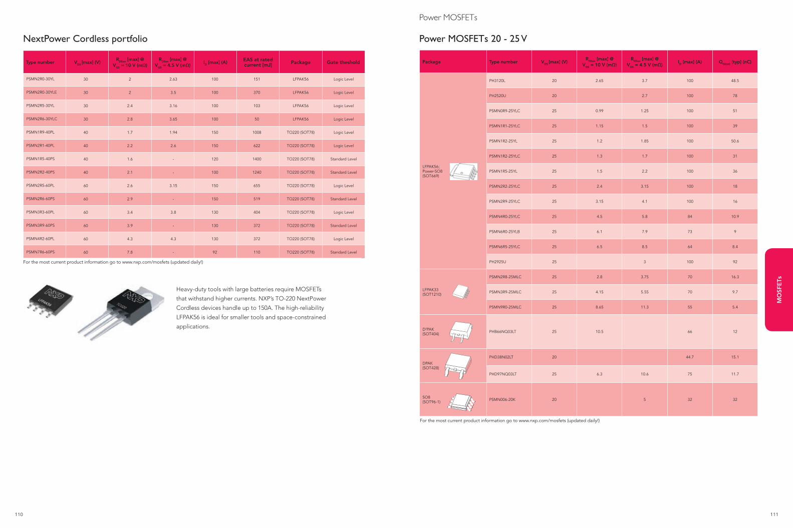
110 111
MO
SFE
Ts
Type number VDS [max] (V)RDSon [max] @
VGS = 10 V (mΩ)RDSon [max] @
VGS = 4.5 V (mΩ)ID [max] (A) EAS at rated
current [mJ] Package Gate theshold Package Type number VDS [max] (V)RDSon [max] @
VGS = 10 V (mΩ)RDSon [max] @
VGS = 4.5 V (mΩ)ID [max] (A) QG(tot) [typ] (nC)
LFPAK56; Power-SO8 (SOT669)
PH3120L 20 2.65 3.7 100 48.5
PH2520U 20 2.7 100 78
PSMN0R9-25YLC 25 0.99 1.25 100 51
PSMN1R1-25YLC 25 1.15 1.5 100 39
PSMN1R2-25YL 25 1.2 1.85 100 50.6
PSMN1R2-25YLC 25 1.3 1.7 100 31
PSMN1R5-25YL 25 1.5 2.2 100 36
PSMN2R2-25YLC 25 2.4 3.15 100 18
PSMN2R9-25YLC 25 3.15 4.1 100 16
PSMN4R0-25YLC 25 4.5 5.8 84 10.9
PSMN6R0-25YLB 25 6.1 7.9 73 9
PSMN6R5-25YLC 25 6.5 8.5 64 8.4
PH2925U 25 3 100 92
LFPAK33(SOT1210)
PSMN2R8-25MLC 25 2.8 3.75 70 16.3
PSMN3R9-25MLC 25 4.15 5.55 70 9.7
PSMN9R0-25MLC 25 8.65 11.3 55 5.4
D2PAK (SOT404) PHB66NQ03LT 25 10.5 66 12
DPAK(SOT428)
PHD38N02LT 20 44.7 15.1
PHD97NQ03LT 25 6.3 10.6 75 11.7
SO8(SOT96-1) PSMN006-20K 20 5 32 32
For the most current product information go to www.nxp.com/mosfets (updated daily!)
Power MOSFETs 20 - 25 VNextPower Cordless portfolio
Power MOSFETs
Heavy-duty tools with large batteries require MOSFETs
that withstand higher currents. NXP’s TO-220 NextPower
Cordless devices handle up to 150A. The high-reliability
LFPAK56 is ideal for smaller tools and space-constrained
applications.
PSMN2R0-30YL
PSMN2R0-30YLE
PSMN2R5-30YL
PSMN2R6-30YLC
PSMN1R9-40PL
PSMN2R1-40PL
PSMN1R5-40PS
PSMN2R2-40PS
PSMN2R5-60PL
PSMN2R6-60PS
PSMN3R3-60PL
PSMN3R9-60PS
PSMN4R2-60PL
PSMN7R6-60PS
30
30
30
30
40
40
40
40
60
60
60
60
60
60
2
2
2.4
2.8
1.7
2.2
1.6
2.1
2.6
2.9
3.4
3.9
4.3
7.8
2.63
3.5
3.16
3.65
1.94
2.6
-
-
3.15
-
3.8
-
4.3
-
100
100
100
100
150
150
120
100
150
150
130
130
130
92
151
370
103
50
1008
622
1400
1240
655
519
404
372
372
110
LFPAK56
LFPAK56
LFPAK56
LFPAK56
TO220 (SOT78)
TO220 (SOT78)
TO220 (SOT78)
TO220 (SOT78)
TO220 (SOT78)
TO220 (SOT78)
TO220 (SOT78)
TO220 (SOT78)
TO220 (SOT78)
TO220 (SOT78)
Logic Level
Logic Level
Logic Level
Logic Level
Logic Level
Logic Level
Standard Level
Standard Level
Logic Level
Standard Level
Logic Level
Standard Level
Logic Level
Standard Level
For the most current product information go to www.nxp.com/mosfets (updated daily!)
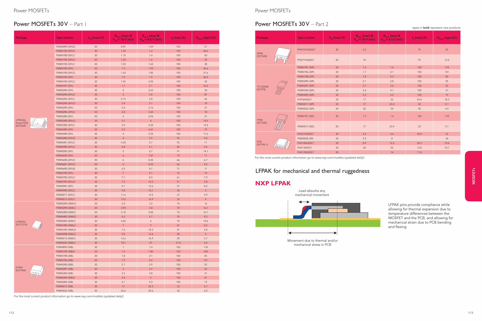
112 113
MO
SFE
Ts
Package Type number VDS [max] (V)RDSon [max] @
VGS = 10 V (mΩ)RDSon [max] @
VGS = 4.5 V (mΩ)ID [max] (A) QG(tot) [typ] (nC)
DPAK(SOT428)
PHD101NQ03LT 30 5.5 75 23
PHD71NQ03LT 30 10 75 13.2
TO-220AB(SOT78)
PSMN1R1-30PL 30 1.3 1.6 120 118
PSMN1R6-30PL 30 1.7 2.1 100 101
PSMN1R8-30PL 30 1.8 2.3 100 83
PSMN2R0-30PL 30 2.1 2.8 100 55
PSMN2R7-30PL 30 2.7 3.6 100 32
PSMN3R4-30PL 30 3.4 4.1 100 31
PSMN4R3-30PL 30 4.3 6.2 100 19
PHP36N03LT 30 17 22 43.4 18.5
PSMN017-30PL 30 17 23.4 32 5.1
PSMN022-30PL 30 22 34 30 4.4
I2PAK(SOT226)
PSMN1R1-30EL 30 1.3 1.6 120 118
PSMN017-30EL 30 17 23.4 32 5.1
SO8(SOT96-1)
PHK31NQ03LT 30 4.4 5.6 30.4 33
PSMN005-30K 30 5.5 8 34
PHK18NQ03LT 30 8.9 12.5 20.3 10.6
PHK13N03LT 30 20 26 13.8 10.7
PHK12NQ03LT 30 14 11.8
Power MOSFETs
Power MOSFETs 30 V – Part 2
LFPAK for mechanical and thermal ruggedness
NXP LFPAKLead absorbs any
mechanical movement
Movement due to thermal and/or mechanical stress in PCB
LFPAK pins provide compliance while allowing for thermal expansion due to temperature differences between the MOSFET and the PCB, and allowing for mechanical strain due to PCB bending and flexing
types in bold represent new products
For the most current product information go to www.nxp.com/mosfets (updated daily!)
Package Type number VDS [max] (V)RDSon [max] @
VGS = 10 V (mΩ)RDSon [max] @
VGS = 4.5 V (mΩ)ID [max] (A) QG(tot) [typ] (nC)
LFPAK56;Power-SO8(SOT669)
PSMN0R9-30YLD 30 0.87 1.09 100 51
PSMN1R0-30YLD 30 1.02 1.3 100 38.2
PSMN1R0-30YLC 30 1.15 1.4 100 50
PSMN1R2-30YLD 30 1.24 1.6 100 32
PSMN1R2-30YLC 30 1.25 1.65 100 38
PSMN1R3-30YL 30 1.3 1.95 100 46.6
PSMN1R4-30YLD 30 1.42 1.85 100 27.6
PSMN1R5-30YL 30 1.5 1.9 100 36.2
PSMN1R5-30YLC 30 1.55 2.05 100 30
PSMN1R7-30YL 30 1.7 2.1 100 36.2
PSMN2R0-30YL 30 2 2.63 100 30
PSMN2R0-30YLE 30 2 3.5 100 87
PSMN2R2-30YLC 30 2.15 2.8 100 26
PSMN2R4-30YLD 30 2.4 3.1 100 18
PSMN2R5-30YL 30 2.4 3.16 100 27
PSMN2R6-30YLC 30 2.8 3.65 100 18
PSMN3R0-30YL 30 3 4.04 100 21
PSMN3R0-30YLD 30 3.1 4 100 14.5
PSMN3R2-30YLC 30 3.5 4.55 100 14.2
PSMN3R5-30YL 30 3.5 4.61 100 19
PSMN4R0-30YL 30 4 5.25 100 17.6
PSMN4R0-30YLD 30 4 5.5 95 9.6
PSMN4R1-30YLC 30 4.35 5.7 92 11
PSMN4R5-30YLC 30 4.8 6.1 84 9.6
PSMN5R0-30YL 30 5 6.7 91 14.1
PSMN6R0-30YL 30 6 7.87 79 11
PSMN6R0-30YLD 30 6 8.35 66 6.7
PSMN6R1-30YLD 30 6 8.35 66 6.4
PSMN6R0-30YLB 30 6.5 8.1 71 9
PSMN7R0-30YL 30 7 9.1 76 10
PSMN7R0-30YLC 30 7.1 8.9 61 7.9
PSMN7R5-30YLD 30 7.5 10.2 51 5.8
PSMN9R1-30YL 30 9.1 13.6 57 8.4
PSMN9R5-30YLC 30 9.8 12.1 44 5
PSMN011-30YLC 30 11.6 14.5 37 4.9
PSMN013-30YLC 30 13.6 16.9 32 4
LFPAK33(SOT1210)
PSMN2R4-30MLD 30 2.4 3.2 70 16
PSMN2R9-30MLC 30 2.95 3.8 70 16.7
PSMN3R0-30MLC 30 3.15 4.05 70 16.1
PSMN4R2-30MLD 30 4.3 5.7 70 9.2
PSMN4R4-30MLC 30 4.65 6 70 10.6
PSMN7R0-30MLC 30 7 9 67 8.2
PSMN7R5-30MLD 30 7.6 10.3 57 5.8
PSMN9R8-30MLC 30 9.8 12.4 50 5
PSMN013-30MLC 30 13.6 16.9 39 3.7
PSMN020-30MLC 30 18.1 27 31.8 4.6
D2PAK(SOT404)
PSMNR90-30BL 30 1 1.4 120 118
PSMN1R5-30BLE 30 1.5 1.85 120 228
PSMN1R8-30BL 30 1.8 2.1 100 83
PSMN1R6-30BL 30 1.9 2.2 100 101
PSMN2R0-30BL 30 2.1 2.9 100 55
PSMN2R7-30BL 30 3 3.7 100 32
PSMN3R4-30BL 30 3.3 3.8 100 31
PSMN3R4-30BLE 30 3.4 5 120 81
PSMN4R3-30BL 30 4.1 5.2 100 19
PSMN017-30BL 30 17 23.3 32 5.1
PSMN022-30BL 30 22.6 29.6 30 4.4
Power MOSFETs
Power MOSFETs 30 V – Part 1
For the most current product information go to www.nxp.com/mosfets (updated daily!)
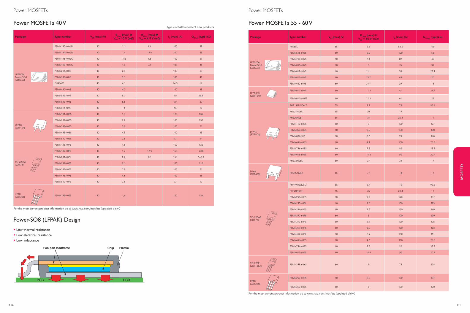
114 115
MO
SFE
Ts
Package Type number VDS [max] (V)RDSon [max] @
VGS = 10 V (mΩ)ID [max] (A) QG(tot) [typ] (nC)
LFPAK56; Power-SO8 (SOT669)
PH955L 55 8.3 62.5 42
PSMN5R5-60YS 60 5.2 100 56
PSMN7R0-60YS 60 6.4 89 45
PSMN8R5-60YS 60 8 76 39
PSMN012-60YS 60 11.1 59 28.4
PSMN017-60YS 60 15.7 44 20
PSMN030-60YS 60 24.7 29 13
LFPAK33 (SOT1210)
PSMN011-60ML 60 11.3 61 37.2
PSMN011-60MS 60 11.3 61 23
D2PAK (SOT404)
PHB191NQ06LT 55 3.7 75 95.6
PHB21N06LT 55 70 19
PHB20N06T 55 75 20.3 11
PSMN1R7-60BS 60 2 120 137
PSMN3R0-60BS 60 3.2 100 130
PSMN004-60B 60 3.6 75 168
PSMN4R6-60BS 60 4.4 100 70.8
PSMN7R6-60BS 60 7.8 92 38.7
PSMN015-60BS 60 14.8 50 20.9
PHB32N06LT 60 37 34 17
DPAK (SOT428) PHD20N06T 55 77 18 11
TO-220AB (SOT78)
PHP191NQ06LT 55 3.7 75 95.6
PHP20N06T 55 75 20.3 11
PSMN2R0-60PS 60 2.2 120 137
PSMN2R5-60PL 60 2.6 150 223
PSMN2R6-60PS 60 2.6 150 140
PSMN3R0-60PS 60 3 100 130
PSMN3R3-60PL 60 3.4 130 175
PSMN3R9-60PS 60 3.9 130 103
PSMN4R2-60PL 60 3.9 130 151
PSMN4R6-60PS 60 4.6 100 70.8
PSMN7R6-60PS 60 7.8 92 38.7
PSMN015-60PS 60 14.8 50 20.9
TO-220F(SOT186A) PSMN3R9-60XS 60 4 75 103
I2PAK (SOT226)
PSMN2R0-60ES 60 2.2 120 137
PSMN3R0-60ES 60 3 100 130
Power MOSFETs
Power MOSFETs 55 - 60 V
For the most current product information go to www.nxp.com/mosfets (updated daily!)
Power MOSFETs
Power MOSFETs 40 V
Package Type number VDS [max] (V)RDSon [max] @
VGS = 10 V (mΩ)RDSon [max] @
VGS = 4.5 V (mΩ)ID [max] (A) QG(tot) [typ] (nC)
LFPAK56; Power-SO8 (SOT669)
PSMN1R0-40YLD 40 1.1 1.4 100 59
PSMN1R4-40YLD 40 1.4 1.85 100 45
PSMN1R6-40YLC 40 1.55 1.8 100 59
PSMN1R8-40YLC 40 1.8 2.1 100 45
PSMN2R6-40YS 40 2.8 100 63
PSMN3R3-40YS 40 3.3 100 49
PH4840S 40 4.1 94.5 67
PSMN4R0-40YS 40 4.2 100 38
PSMN5R8-40YS 40 5.7 90 28.8
PSMN8R3-40YS 40 8.6 70 20
PSMN014-40YS 40 14 46 12
D2PAK (SOT404)
PSMN1R1-40BS 40 1.3 120 136
PSMN2R2-40BS 40 2.2 100 130
PSMN2R8-40BS 40 2.9 100 71
PSMN4R5-40BS 40 4.5 100 35
PSMN8R0-40BS 40 7.6 77 21
TO-220AB(SOT78)
PSMN1R5-40PS 40 1.6 150 136
PSMN1R9-40PL 40 1.7 1.94 150 230
PSMN2R1-40PL 40 2.2 2.6 150 168.9
PSMN2R2-40PS 40 2.1 100 110
PSMN2R8-40PS 40 2.8 100 71
PSMN4R5-40PS 40 4.6 100 35
PSMN8R0-40PS 40 7.6 77 17
I2PAK (SOT226) PSMN1R5-40ES 40 1,6 120 136
types in bold represent new products
For the most current product information go to www.nxp.com/mosfets (updated daily!)
Power-SO8 (LFPAK) Design
Low thermal resistance
Low electrical resistance
Low inductance
bra187
BCPBCP
Chip PlasticTwo-part leadframe
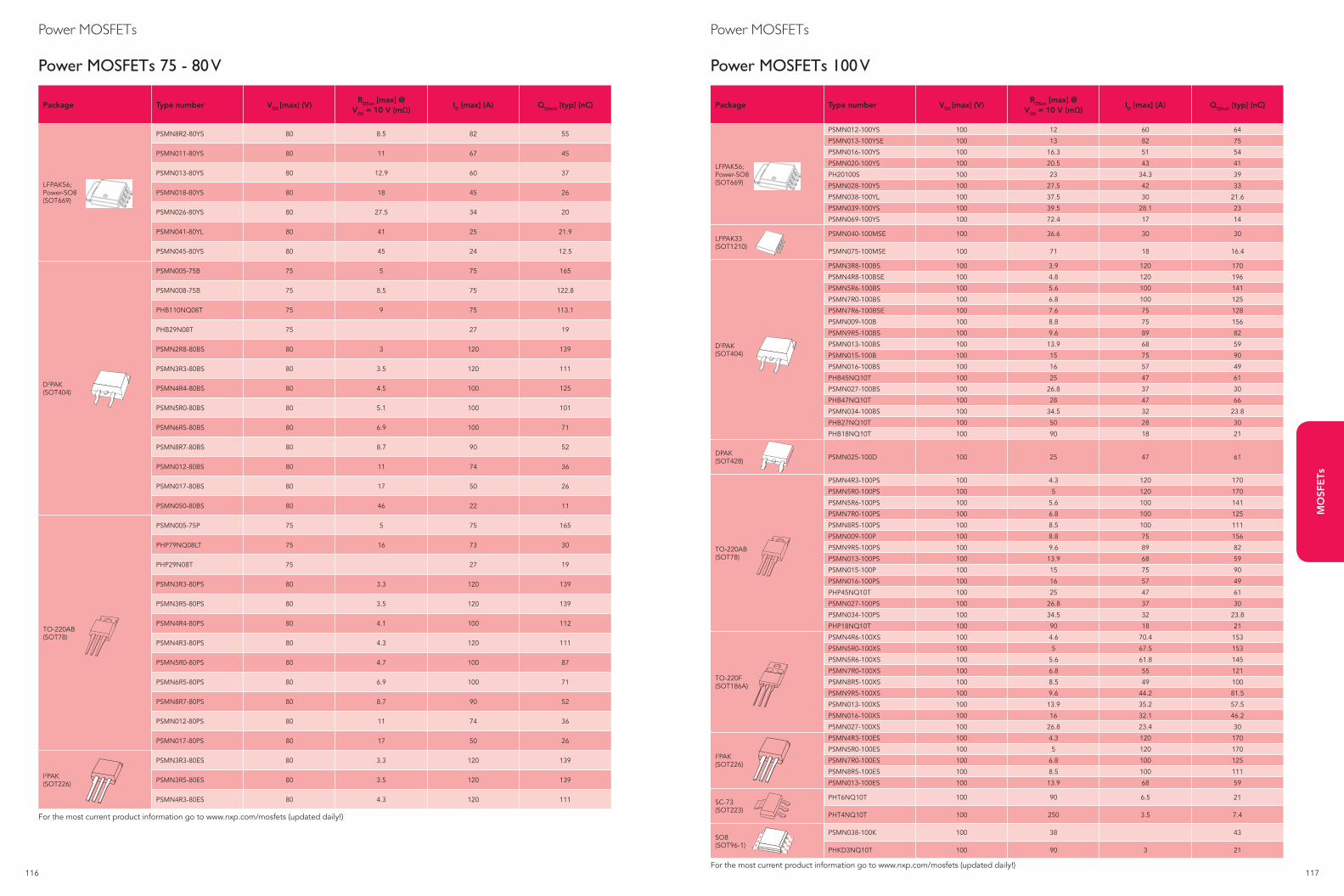
116 117
MO
SFE
Ts
Package Type number VDS [max] (V)RDSon [max] @
VGS = 10 V (mΩ)ID [max] (A) QG(tot) [typ] (nC)
LFPAK56; Power-SO8 (SOT669)
PSMN012-100YS 100 12 60 64
PSMN013-100YSE 100 13 82 75
PSMN016-100YS 100 16.3 51 54
PSMN020-100YS 100 20.5 43 41
PH20100S 100 23 34.3 39
PSMN028-100YS 100 27.5 42 33
PSMN038-100YL 100 37.5 30 21.6
PSMN039-100YS 100 39.5 28.1 23
PSMN069-100YS 100 72.4 17 14
LFPAK33 (SOT1210)
PSMN040-100MSE 100 36.6 30 30
PSMN075-100MSE 100 71 18 16.4
D2PAK (SOT404)
PSMN3R8-100BS 100 3.9 120 170
PSMN4R8-100BSE 100 4.8 120 196
PSMN5R6-100BS 100 5.6 100 141
PSMN7R0-100BS 100 6.8 100 125
PSMN7R6-100BSE 100 7.6 75 128
PSMN009-100B 100 8.8 75 156
PSMN9R5-100BS 100 9.6 89 82
PSMN013-100BS 100 13.9 68 59
PSMN015-100B 100 15 75 90
PSMN016-100BS 100 16 57 49
PHB45NQ10T 100 25 47 61
PSMN027-100BS 100 26.8 37 30
PHB47NQ10T 100 28 47 66
PSMN034-100BS 100 34.5 32 23.8
PHB27NQ10T 100 50 28 30
PHB18NQ10T 100 90 18 21
DPAK (SOT428) PSMN025-100D 100 25 47 61
TO-220AB (SOT78)
PSMN4R3-100PS 100 4.3 120 170
PSMN5R0-100PS 100 5 120 170
PSMN5R6-100PS 100 5.6 100 141
PSMN7R0-100PS 100 6.8 100 125
PSMN8R5-100PS 100 8.5 100 111
PSMN009-100P 100 8.8 75 156
PSMN9R5-100PS 100 9.6 89 82
PSMN013-100PS 100 13.9 68 59
PSMN015-100P 100 15 75 90
PSMN016-100PS 100 16 57 49
PHP45NQ10T 100 25 47 61
PSMN027-100PS 100 26.8 37 30
PSMN034-100PS 100 34.5 32 23.8
PHP18NQ10T 100 90 18 21
TO-220F (SOT186A)
PSMN4R6-100XS 100 4.6 70.4 153
PSMN5R0-100XS 100 5 67.5 153
PSMN5R6-100XS 100 5.6 61.8 145
PSMN7R0-100XS 100 6.8 55 121
PSMN8R5-100XS 100 8.5 49 100
PSMN9R5-100XS 100 9.6 44.2 81.5
PSMN013-100XS 100 13.9 35.2 57.5
PSMN016-100XS 100 16 32.1 46.2
PSMN027-100XS 100 26.8 23.4 30
I2PAK (SOT226)
PSMN4R3-100ES 100 4.3 120 170
PSMN5R0-100ES 100 5 120 170
PSMN7R0-100ES 100 6.8 100 125
PSMN8R5-100ES 100 8.5 100 111
PSMN013-100ES 100 13.9 68 59
SC-73(SOT223)
PHT6NQ10T 100 90 6.5 21
PHT4NQ10T 100 250 3.5 7.4
SO8 (SOT96-1)
PSMN038-100K 100 38 43
PHKD3NQ10T 100 90 3 21
Power MOSFETs 100 V
Power MOSFETs
For the most current product information go to www.nxp.com/mosfets (updated daily!)
Power MOSFETs 75 - 80 V
Package Type number VDS [max] (V)RDSon [max] @
VGS = 10 V (mΩ)ID [max] (A) QG(tot) [typ] (nC)
LFPAK56; Power-SO8 (SOT669)
PSMN8R2-80YS 80 8.5 82 55
PSMN011-80YS 80 11 67 45
PSMN013-80YS 80 12.9 60 37
PSMN018-80YS 80 18 45 26
PSMN026-80YS 80 27.5 34 20
PSMN041-80YL 80 41 25 21.9
PSMN045-80YS 80 45 24 12.5
D2PAK (SOT404)
PSMN005-75B 75 5 75 165
PSMN008-75B 75 8.5 75 122.8
PHB110NQ08T 75 9 75 113.1
PHB29N08T 75 27 19
PSMN2R8-80BS 80 3 120 139
PSMN3R3-80BS 80 3.5 120 111
PSMN4R4-80BS 80 4.5 100 125
PSMN5R0-80BS 80 5.1 100 101
PSMN6R5-80BS 80 6.9 100 71
PSMN8R7-80BS 80 8.7 90 52
PSMN012-80BS 80 11 74 36
PSMN017-80BS 80 17 50 26
PSMN050-80BS 80 46 22 11
TO-220AB (SOT78)
PSMN005-75P 75 5 75 165
PHP79NQ08LT 75 16 73 30
PHP29N08T 75 27 19
PSMN3R3-80PS 80 3.3 120 139
PSMN3R5-80PS 80 3.5 120 139
PSMN4R4-80PS 80 4.1 100 112
PSMN4R3-80PS 80 4.3 120 111
PSMN5R0-80PS 80 4.7 100 87
PSMN6R5-80PS 80 6.9 100 71
PSMN8R7-80PS 80 8.7 90 52
PSMN012-80PS 80 11 74 36
PSMN017-80PS 80 17 50 26
I2PAK (SOT226)
PSMN3R3-80ES 80 3.3 120 139
PSMN3R5-80ES 80 3.5 120 139
PSMN4R3-80ES 80 4.3 120 111
Power MOSFETs
For the most current product information go to www.nxp.com/mosfets (updated daily!)
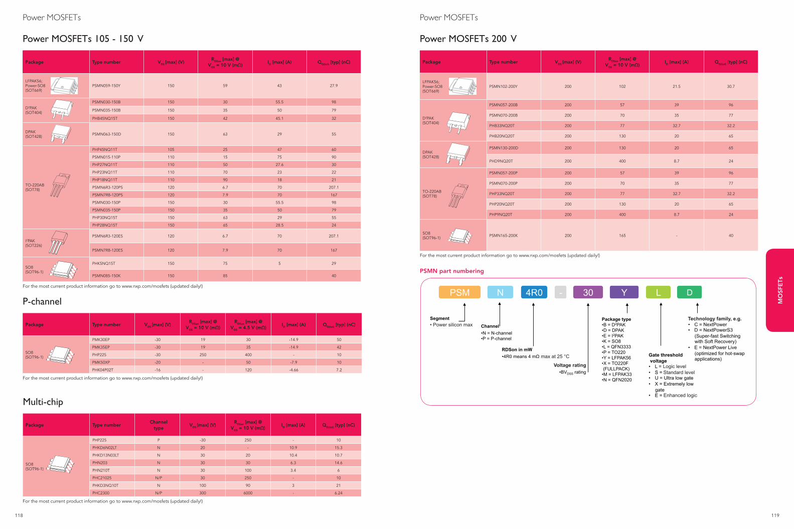
118 119
MO
SFE
Ts
Package Typenumber VDS [max] (V)RDSon [max] @
VGS = 10 V (mΩ)ID [max] (A) QG(tot) [typ] (nC)
LFPAK56; Power-SO8 (SOT669)
PSMN059-150Y 150 59 43 27.9
D2PAK (SOT404)
PSMN030-150B 150 30 55.5 98
PSMN035-150B 150 35 50 79
PHB45NQ15T 150 42 45.1 32
DPAK (SOT428) PSMN063-150D 150 63 29 55
TO-220AB(SOT78)
PHP45NQ11T 105 25 47 60
PSMN015-110P 110 15 75 90
PHP27NQ11T 110 50 27.6 30
PHP23NQ11T 110 70 23 22
PHP18NQ11T 110 90 18 21
PSMN6R3-120PS 120 6.7 70 207.1
PSMN7R8-120PS 120 7.9 70 167
PSMN030-150P 150 30 55.5 98
PSMN035-150P 150 35 50 79
PHP30NQ15T 150 63 29 55
PHP28NQ15T 150 65 28.5 24
I2PAK (SOT226)
PSMN6R3-120ES 120 6.7 70 207.1
PSMN7R8-120ES 120 7.9 70 167
SO8 (SOT96-1)
PHK5NQ15T 150 75 5 29
PSMN085-150K 150 85 40
Package Type number VDS [max] (V)RDSon [max] @
VGS = 10 V (mΩ)ID [max] (A) QG(tot) [typ] (nC)
LFPAK56; Power-SO8 (SOT669)
PSMN059-150Y 150 59 43 27.9
D2PAK (SOT404)
PSMN030-150B 150 30 55.5 98
PSMN035-150B 150 35 50 79
PHB45NQ15T 150 42 45.1 32
DPAK (SOT428) PSMN063-150D 150 63 29 55
TO-220AB(SOT78)
PHP45NQ11T 105 25 47 60
PSMN015-110P 110 15 75 90
PHP27NQ11T 110 50 27.6 30
PHP23NQ11T 110 70 23 22
PHP18NQ11T 110 90 18 21
PSMN6R3-120PS 120 6.7 70 207.1
PSMN7R8-120PS 120 7.9 70 167
PSMN030-150P 150 30 55.5 98
PSMN035-150P 150 35 50 79
PHP30NQ15T 150 63 29 55
PHP28NQ15T 150 65 28.5 24
I2PAK (SOT226)
PSMN6R3-120ES 120 6.7 70 207.1
PSMN7R8-120ES 120 7.9 70 167
SO8 (SOT96-1)
PHK5NQ15T 150 75 5 29
PSMN085-150K 150 85 40
Package Type number VDS [max] (V)RDSon [max] @
VGS = 10 V (mΩ)ID [max] (A) QG(tot) [typ] (nC)
LFPAK56; Power-SO8(SOT669)
PSMN102-200Y 200 102 21.5 30.7
D2PAK (SOT404)
PSMN057-200B 200 57 39 96
PSMN070-200B 200 70 35 77
PHB33NQ20T 200 77 32.7 32.2
PHB20NQ20T 200 130 20 65
DPAK (SOT428)
PSMN130-200D 200 130 20 65
PHD9NQ20T 200 400 8.7 24
TO-220AB(SOT78)
PSMN057-200P 200 57 39 96
PSMN070-200P 200 70 35 77
PHP33NQ20T 200 77 32.7 32.2
PHP20NQ20T 200 130 20 65
PHP9NQ20T 200 400 8.7 24
SO8 (SOT96-1) PSMN165-200K 200 165 - 40
For the most current product information go to www.nxp.com/mosfets (updated daily!)
Power MOSFETs
Power MOSFETs 200 VPower MOSFETs 105 - 150 V
Power MOSFETs
For the most current product information go to www.nxp.com/mosfets (updated daily!)
P-channel
Package Type number VDS [max] (V)RDSon [max] @
VGS = 10 V (mΩ)RDSon [max] @
VGS = 4.5 V (mΩ)ID [max] (A) QG(tot) [typ] (nC)
SO8 (SOT96-1)
PMK30EP -30 19 30 -14.9 50
PMK35EP -30 19 35 -14.9 42
PHP225 -30 250 400 - 10
PMK50XP -20 - 50 -7.9 10
PHK04P02T -16 - 120 -4.66 7.2
For the most current product information go to www.nxp.com/mosfets (updated daily!)
Multi-chip
Package Type numberChannel
typeVDS [max] (V)
RDSon [max] @ VGS = 10 V (mΩ)
ID [max] (A) QG(tot) [typ] (nC)
SO8 (SOT96-1)
PHP225 P -30 250 - 10
PHKD6N02LT N 20 - 10.9 15.3
PHKD13N03LT N 30 20 10.4 10.7
PHN203 N 30 30 6.3 14.6
PHN210T N 30 100 3.4 6
PHC21025 N/P 30 250 - 10
PHKD3NQ10T N 100 90 3 21
PHC2300 N/P 300 6000 - 6.24
For the most current product information go to www.nxp.com/mosfets (updated daily!)
PSMN part numbering
Technology family, e.g.• Power silicon max
max at 25 °C
Logic levelStandard level
Enhanced logic
Voltage rating

120 121
MO
SFE
Ts
Quick learning videos
Reverse recovery and diode leakage
in SMPS
www.nxp.com/quicklearning33
NextPowerS3 MOSFETs for DC/DC buck regulators
www.nxp.com/quicklearning32
Power MOSFET operation in Linear Mode
www.nxp.com/quicklearning34
MOSFETs for Power-over-Ethernet (PoE) PSE applications
www.nxp.com/quicklearning36
Next Power Live! MOSFETs for HOT SWAP and Power over Ethernet
www.nxp.com/quicklearning29
Single-shot avalance ruggedness
www.nxp.com/quicklearning35
NextPower Cordless MOSFETs for
battery-powered tools
www.nxp.com/quicklearning28
LFPAK Power-SO8 vs. DPAK
www.nxp.com/quicklearning18
Introducing NXP LFPAK
www.nxp.com/quicklearning5
Introduction to clip-bonding technology
www.nxp.com/quicklearning1
Small-signal MOSFETs for automotive
DFN1010 and DFN2020 with solderable side pads
Comparison of solder capability Reference design for LED lighting
NXP package100% solderable side pads
100% solder wetting solution with new 2 x 2 mm leadless package DFN2020MD-6
Quality of solder connection difficult to determine
Very limited options for optical solder inspection
Packages from other suppliers
In t
he s
po
tlig
ht PMPB85ENEA - Automotive-compliant 60 V N-channel MOSFET with ID max of 4.4 A in DFN2020MD-6 (SOT1220)
60 V N-channel with RDSon of typ. 72mΩ @ VGS = 10 V
Small and leadless ultrathin SMD plastic package: 2.0 x 2.0 x 0.65 mm
Exposed drain pad for excellent thermal conduction
ESD protection to 2 kV HBM
AEC-Q101 qualified
High-quality solder connections
No complete wetting on side pad
Reduction of production costs through
optical visual solder inspection

122 123
MO
SFE
Ts
Automotive MOSFETs
types in bold represent new products
Automotive MOSFETs
Automotive-compliant small-signal MOSFETs
Package
SOT223SOT457 (SC-74)
SOT23SOT363 (SC-88)
SOT323 (SC-70)
SOT666DFN2020MD-6
(SOT1220)DFN1010D-3
(SOT1215)DFN1006 (SOT883)
Size (mm) 6.5 x 3.5 x 1.65 2.9 x 1.5 x 1.0 2.9 x 1.3 x 1.0 2.0 x 1.25 x 0.95 2.0 x 1.25 x 0.95 1.6 x 1.2 x 0.55 2.0 x 2.0 x 0.65 1.1 x 1.0 x 0.37 1.0 x 0.6 x 0.5
Ptot (mW) 1700 600 250 300 200 300 1250 1000 250
Polarity Configuration VDS (V) VGS (V) ID (A)VGS(th)
min (V)VGS(th)
max (V)ton typ
(ns)toff typ
(ns)QG typ
(nC)
ESD protection
(kV)
RDSon typ (mΩ) @ VGS =
10 V 4.5 V 2.5 V 1.8 V
N-c
hann
el
Single
208 5.2 0.5 1.5 12 128 6.4 2 - 24 28 72 PMV28UNEA
12 5.9 0.75 1.25 16 49 31 2 - 14 20 - PMV20XNEA
30
8 0.4 0.6 1.1 26 88 0.52 2 - 1000 1400 2000 NX3008NBK NX3008NBKW
20
4.9 1 2.5 9.9 29 20 2.8 15 21 - - PMV25ENEA
3.7 1 2.5 - - - 1.6 - - - - PMV50ENEA
1.9 1 2.5 5.4 12 5.4 1.6 54 74 - - PMV100ENEA
40 20 2.5 1 2.5 14 14 2.4 1 95 120 - - PMV130ENEA
60 20
12.9 1 3 9 12 12.1 - 34 40 - - PMPB40SNA
- 1.3 2.7 - - - 2 44 52 - - PMPB55ENEA
2.8 1 2.5 9 33 19 2.8 46 52 - - PMV55ENEA
3 1.3 2.7 4 10.5 6.2 2.7 72 85 - - PMPB85ENEA
1.9 1 2.5 - - - 2 - - - - PMV120ENEA
1.4 1 2.5 - - - 2 - - - - PMV230ENEA
0.7 1 2.5 - - - 2.5 - - - - PMV450ENEA
0.36 0.9 1.5 5 13 0.72 - 900 1000 - - BSS138P BSS138PW
0.36 0.48 1.6 10 58 0.6 1.5 1000 1100 1400 - BSS138BK BSS138BKW
0.3 1 2.5 11 19 0.5 2 1000 1300 - - 2N7002BK 2N7002BKW 2N7002BKM
0.3 1 2.5 16 60 1.09 3 1100 1300 - - 2N7002CK
0.2 0.8 1.5 5 36 0.39 Yes 2700 3000 4000 - BSS138AKA
80 20
1.9 1.3 2.7 3.5 9.5 4.8 2 175 195 - - PMPB215ENEA
2.8 1.3 2.7 5 15 9.9 2.8 80 92 - - PMPB95ENEA
1.1 1.3 2.7 2 9 3 2 345 390 - - PMXB360ENEA
100 20- 1.3 2.7 - - - 2 275 300 - - PMT280ENEA
- 1.3 2.7 - - - 2 520 560 - - PMT560ENEA
Dual
20 8 0.8 0.5 0.95 10 117 0.45 2 - 380 620 1100 PMDT290UNE
30 8 0.4 0.6 1.1 26 88 0.52 2 - 1000 1400 2000 NX3008NBKS NX3008NBKV
60 20
0.3 1 2.5 11 19 0.5 2 1000 1300 - - 2N7002BKS
0.36 0.48 1.6 10 58 0.6 1.5 1000 1100 1400 - BSS138BKS
0.36 0.9 1.5 5 13 0.72 - 900 1000 - - BSS138PS
P-ch
anne
l Single
20
86 0.45 0.95 8 50 15.6 4 - 37 45 59 PMN40UPEA
2 0.5 1.1 7 50 6 - - 100 155 210 NX2301P
12
5.7 0.75 1.25 15 37 15 2 - 27 39 - PMN27XPEA
5.7 0.75 1.25 17 33 11.5 2 - 41 56 - PMN42XPEA
4.4 0.75 1.25 - - - 2 - 26 - - PMV30XPEA
3.5 0.75 1.25 11 61 8.5 - - 48 71 - PMV48XPA
4.1 0.75 1.25 15 51 8.7 - - 48 72 - PMN48XPA
3.3 0.75 1.25 7 36 5 2 - 67 99 - PMV65XPEA
4.1 0.75 1.25 7 40 5.2 2 - 70 101 - PMN70XPEA
2.2 0.75 1.25 - - - 2 - 93 - - PMV100XPEA
308 0.23 0.6 1.1 49 103 0.55 2 - 2800 5300 - NX3008PBK NX3008PBKW
20 4 1 3 6 38 18 3 23 39 - - PMV50EPEA
40 20 1.5 1 2.5 4 26 4.7 1 180 220 - - PMV250EPEA
50 20 0.2 1.1 2.1 24 73 0.26 1 5300 6000 - - BSS84AK BSS84AKW BSS84AKM
60 202.2 1 3 - - - 2 99 110 - - PMV100EPEA
0.9 1 3 - - - 2 217 241 - - PMV240EPEA
70 20 2.3 1 3 - - - 2 156 177 - - PMT200EPEA
Dual
20 8 0.55 0.5 1.3 48 152 0.76 2 - 670 1200 1800 PMDT670UPE
30 8 0.2 0.6 1.1 49 103 0.55 2 - 2800 5300 - NX3008PBKS NX3008PBKV
50 20 0.16 1.1 2.1 24 73 0.26 1 5300 6000 - - BSS84AKS BSS84AKV
NCompl
20 8 0.73 0.5 0.95 10 117 0.45 2 - 290 420 600PMGD290UCEA
P 20 8 0.5 0.5 1.3 48 152 0.76 2 - 670 1200 1800
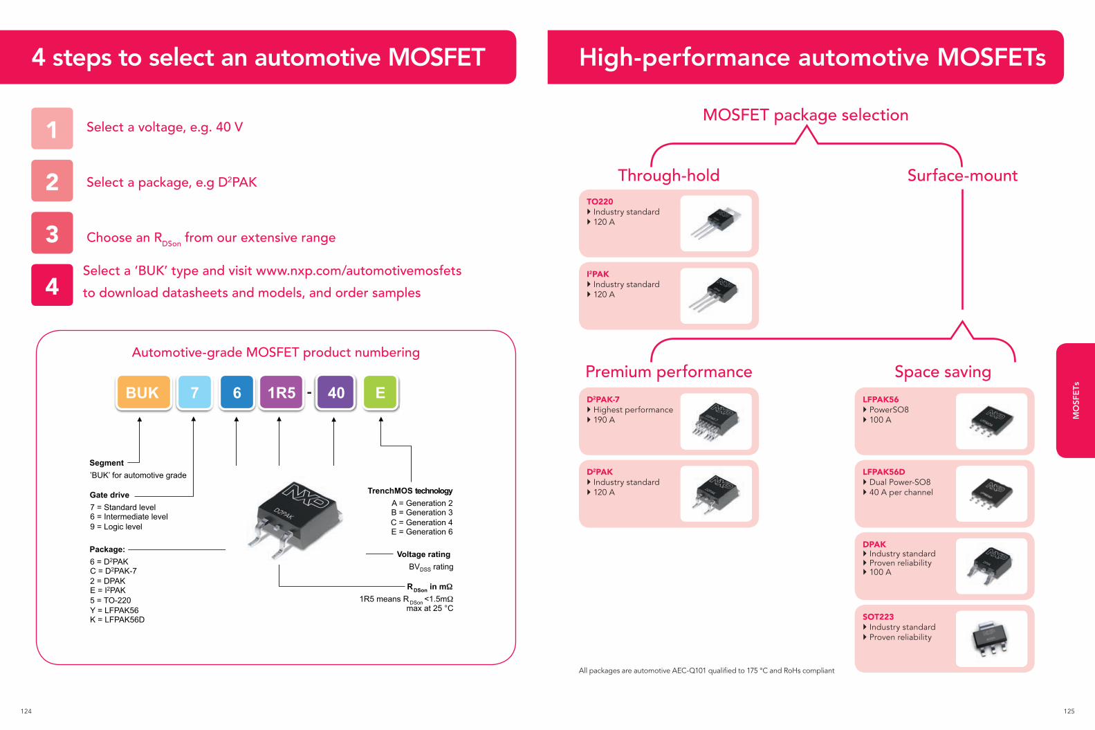
124 125
MO
SFE
Ts
4 steps to select an automotive MOSFET High-performance automotive MOSFETs
Select a voltage, e.g. 40 VMOSFET package selection
Through-hold
Premium performance
Surface-mount
Space saving
Select a package, e.g D2PAK
Choose an RDSon from our extensive range
Select a ‘BUK’ type and visit www.nxp.com/automotivemosfets
to download datasheets and models, and order samples
1
2
3
4
TO220 Industry standard 120 A
I2PAK Industry standard 120 A
D2PAK-7 Highest performance 190 A
D2PAK Industry standard 120 A
All packages are automotive AEC-Q101 qualified to 175 °C and RoHs compliant
LFPAK56 PowerSO8 100 A
LFPAK56D Dual Power-SO8 40 A per channel
DPAK Industry standard Proven reliability 100 A
SOT223 Industry standard Proven reliability
BUK 7 6 1R5 40 E
Segment ’BUK’ for automotive grade
Gate drive 7 = Standard level 6 = Intermediate level 9 = Logic level
Package: 6 = D2PAK C = D2PAK-7 2 = DPAK E = I2PAK 5 = TO-220 Y = LFPAK56 K = LFPAK56D
in m1R5 means <1.5m
max at 25 °C
Voltage ratingBVDSS rating
TrenchMOS technologyA = Generation 2 B = Generation 3 C = Generation 4 E = Generation 6
Automotive-grade MOSFET product numbering
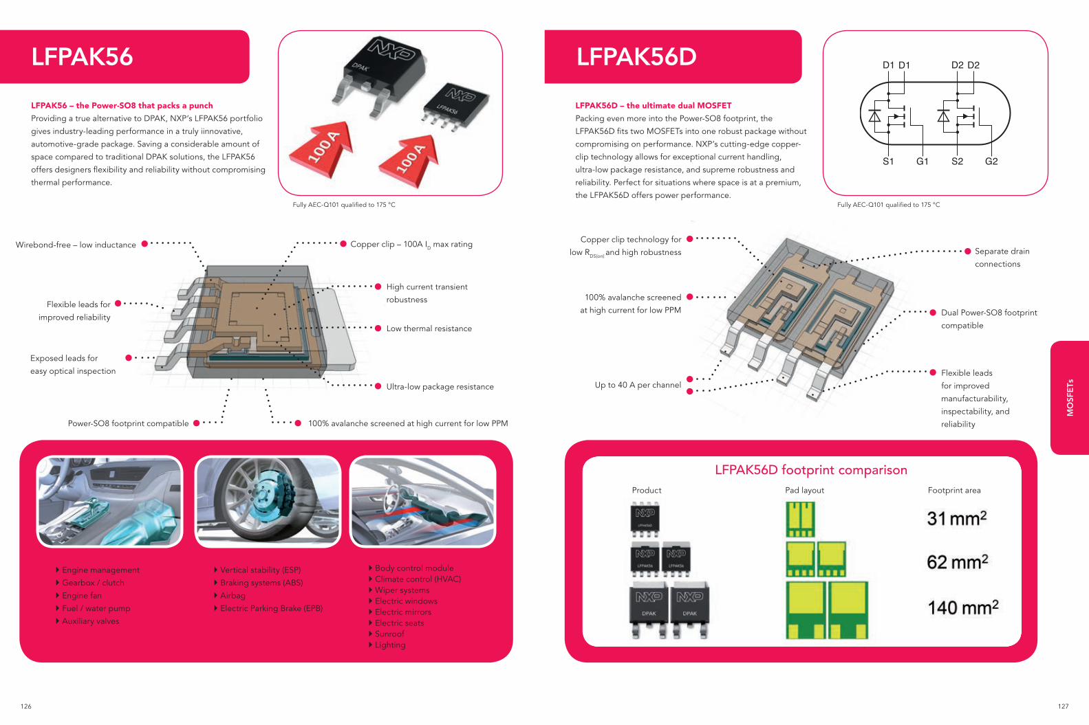
126 127
MO
SFE
Ts
Copper clip technology for
low RDS(on) and high robustness
100% avalanche screened
at high current for low PPM
Up to 40 A per channel
Separate drain
connections
Flexible leads
for improved
manufacturability,
inspectability, and
reliability
Dual Power-SO8 footprint
compatible
LFPAK56 LFPAK56D
LFPAK56 – the Power-SO8 that packs a punch
Providing a true alternative to DPAK, NXP’s LFPAK56 portfolio
gives industry-leading performance in a truly iinnovative,
automotive-grade package. Saving a considerable amount of
space compared to traditional DPAK solutions, the LFPAK56
offers designers flexibility and reliability without compromising
thermal performance.
LFPAK56D – the ultimate dual MOSFET
Packing even more into the Power-SO8 footprint, the
LFPAK56D fits two MOSFETs into one robust package without
compromising on performance. NXP’s cutting-edge copper-
clip technology allows for exceptional current handling,
ultra-low package resistance, and supreme robustness and
reliability. Perfect for situations where space is at a premium,
the LFPAK56D offers power performance.Fully AEC-Q101 qualified to 175 °C Fully AEC-Q101 qualified to 175 °C
Wirebond-free – low inductance Copper clip – 100A ID max rating
High current transient
robustness
Low thermal resistance
Ultra-low package resistance
Exposed leads for
easy optical inspection
Power-SO8 footprint compatible 100% avalanche screened at high current for low PPM
Flexible leads for
improved reliability
POWERTRAIN
Engine management
Gearbox / clutch
Engine fan
Fuel / water pump
Auxiliary valves
CHASSIS & SAFETY
Vertical stability (ESP)
Braking systems (ABS)
Airbag
Electric Parking Brake (EPB)
BODY & SECURITY Body control module Climate control (HVAC) Wiper systems Electric windows Electric mirrors Electric seats Sunroof Lighting
LFPAK56D footprint comparisonProduct Pad layout Footprint area
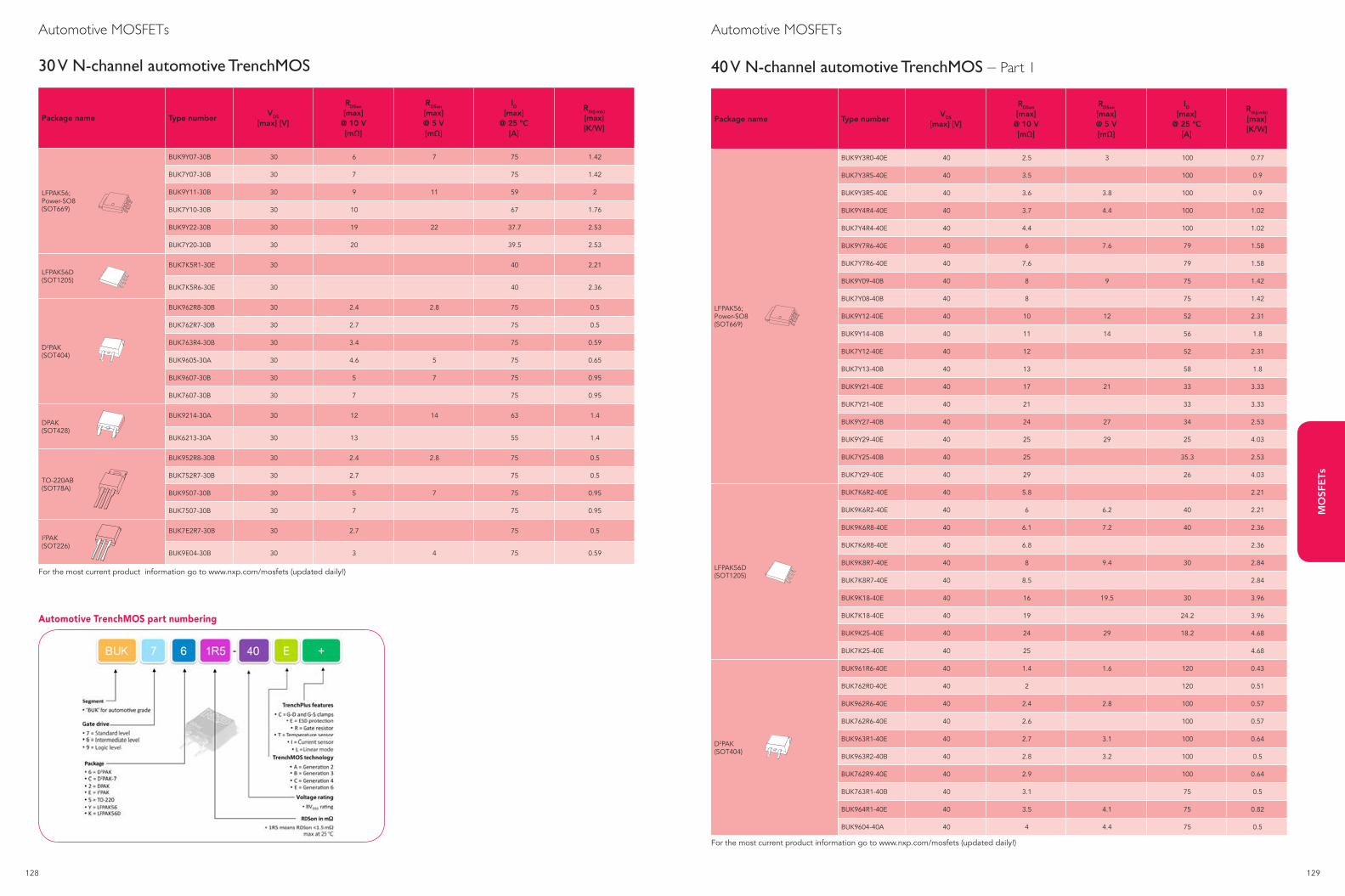
128 129
MO
SFE
Ts
For the most current product information go to www.nxp.com/mosfets (updated daily!)
For the most current product information go to www.nxp.com/mosfets (updated daily!)
Package name Type numberVDS
[max] [V]
RDSon [max]
@ 10 V [mΩ]
RDSon [max] @ 5 V [mΩ]
ID [max]
@ 25 °C [A]
Rth(j-mb) [max] [K/W]
LFPAK56; Power-SO8 (SOT669)
BUK9Y3R0-40E 40 2.5 3 100 0.77
BUK7Y3R5-40E 40 3.5 100 0.9
BUK9Y3R5-40E 40 3.6 3.8 100 0.9
BUK9Y4R4-40E 40 3.7 4.4 100 1.02
BUK7Y4R4-40E 40 4.4 100 1.02
BUK9Y7R6-40E 40 6 7.6 79 1.58
BUK7Y7R6-40E 40 7.6 79 1.58
BUK9Y09-40B 40 8 9 75 1.42
BUK7Y08-40B 40 8 75 1.42
BUK9Y12-40E 40 10 12 52 2.31
BUK9Y14-40B 40 11 14 56 1.8
BUK7Y12-40E 40 12 52 2.31
BUK7Y13-40B 40 13 58 1.8
BUK9Y21-40E 40 17 21 33 3.33
BUK7Y21-40E 40 21 33 3.33
BUK9Y27-40B 40 24 27 34 2.53
BUK9Y29-40E 40 25 29 25 4.03
BUK7Y25-40B 40 25 35.3 2.53
BUK7Y29-40E 40 29 26 4.03
LFPAK56D (SOT1205)
BUK7K6R2-40E 40 5.8 2.21
BUK9K6R2-40E 40 6 6.2 40 2.21
BUK9K6R8-40E 40 6.1 7.2 40 2.36
BUK7K6R8-40E 40 6.8 2.36
BUK9K8R7-40E 40 8 9.4 30 2.84
BUK7K8R7-40E 40 8.5 2.84
BUK9K18-40E 40 16 19.5 30 3.96
BUK7K18-40E 40 19 24.2 3.96
BUK9K25-40E 40 24 29 18.2 4.68
BUK7K25-40E 40 25 4.68
D2PAK (SOT404)
BUK961R6-40E 40 1.4 1.6 120 0.43
BUK762R0-40E 40 2 120 0.51
BUK962R6-40E 40 2.4 2.8 100 0.57
BUK762R6-40E 40 2.6 100 0.57
BUK963R1-40E 40 2.7 3.1 100 0.64
BUK963R2-40B 40 2.8 3.2 100 0.5
BUK762R9-40E 40 2.9 100 0.64
BUK763R1-40B 40 3.1 75 0.5
BUK964R1-40E 40 3.5 4.1 75 0.82
BUK9604-40A 40 4 4.4 75 0.5
Automotive MOSFETs
40 V N-channel automotive TrenchMOS – Part 1
Package name Type numberVDS
[max] [V]
RDSon [max]
@ 10 V [mΩ]
RDSon [max] @ 5 V [mΩ]
ID [max]
@ 25 °C [A]
Rth(j-mb) [max] [K/W]
LFPAK56; Power-SO8 (SOT669)
BUK9Y07-30B 30 6 7 75 1.42
BUK7Y07-30B 30 7 75 1.42
BUK9Y11-30B 30 9 11 59 2
BUK7Y10-30B 30 10 67 1.76
BUK9Y22-30B 30 19 22 37.7 2.53
BUK7Y20-30B 30 20 39.5 2.53
LFPAK56D (SOT1205)
BUK7K5R1-30E 30 40 2.21
BUK7K5R6-30E 30 40 2.36
D2PAK (SOT404)
BUK962R8-30B 30 2.4 2.8 75 0.5
BUK762R7-30B 30 2.7 75 0.5
BUK763R4-30B 30 3.4 75 0.59
BUK9605-30A 30 4.6 5 75 0.65
BUK9607-30B 30 5 7 75 0.95
BUK7607-30B 30 7 75 0.95
DPAK (SOT428)
BUK9214-30A 30 12 14 63 1.4
BUK6213-30A 30 13 55 1.4
TO-220AB (SOT78A)
BUK952R8-30B 30 2.4 2.8 75 0.5
BUK752R7-30B 30 2.7 75 0.5
BUK9507-30B 30 5 7 75 0.95
BUK7507-30B 30 7 75 0.95
I2PAK (SOT226)
BUK7E2R7-30B 30 2.7 75 0.5
BUK9E04-30B 30 3 4 75 0.59
30 V N-channel automotive TrenchMOS
Automotive MOSFETs
Automotive TrenchMOS part numbering
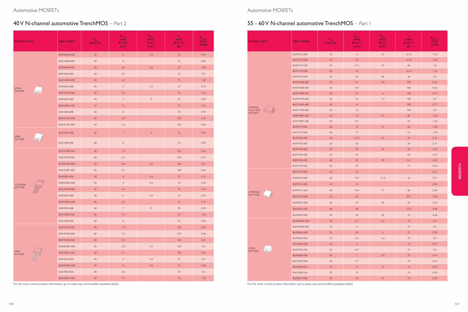
130 131
MO
SFE
Ts
For the most current produc information go to www.nxp.com/mosfets (updated daily!) For the most current produc information go to www.nxp.com/mosfets (updated daily!)
Package name Type numberVDS
[max] [V]
RDSon [max]
@ 10 V [mΩ]
RDSon [max] @ 5 V [mΩ]
ID [max]
@ 25 °C [A]
Rth(j-mb) [max] [K/W]
D2PAK (SOT404)
BUK964R4-40B 40 4 4.4 75 0.59
BUK764R0-40E 40 4 75 0.82
BUK965R4-40E 40 4.4 5.4 75 1.09
BUK7604-40A 40 4.5 75 0.5
BUK765R3-40E 40 4.9 75 1.09
BUK9606-40B 40 5 6.4 75 0.74
BUK765R2-40B 40 5.2 75 0.74
BUK9609-40B 40 7 9 75 0.95
BUK768R1-40E 40 7.2 75 1.56
BUK7608-40B 40 8 75 0.95
BUK761R6-40E 40 1.57 120 0.43
BUK761R7-40E 40 1.6 120 0.46
DPAK(SOT428)
BUK9209-40B 40 7 9 75 0.95
BUK7208-40B 40 8 75 0.95
TO-220AB (SOT78A)
BUK751R8-40E 40 1.8 120 0.43
BUK752R3-40E 40 2.3 120 0.51
BUK953R2-40B 40 2.8 3.2 100 0.5
BUK753R1-40E 40 3.1 100 0.64
BUK9504-40A 40 4 4.4 75 0.5
BUK954R4-40B 40 4 4.4 75 0.59
BUK754R3-40B 40 4.3 75 0.59
BUK9506-40B 40 5 6.4 75 0.74
BUK755R2-40B 40 5.2 75 0.74
BUK9509-40B 40 7 9 75 0.95
BUK758R3-40E 40 7.4 75 1.56
BUK7508-40B 40 8 75 0.95
I2PAK (SOT226)
BUK7E1R8-40E 40 1.8 120 0.43
BUK7E1R9-40E 40 1.9 120 0.46
BUK7E2R3-40E 40 2.3 120 0.51
BUK9E3R2-40B 40 2.8 3.2 100 0.5
BUK7E3R1-40E 40 3.1 100 0.64
BUK9E04-40A 40 4 4.4 75 0.5
BUK9E4R4-40B 40 4 4.4 75 0.59
BUK7E04-40A 40 4.5 75 0.5
BUK7E8R3-40E 40 7.4 75 1.56
Package name Type numberVDS
[max] [V]
RDSon [max]
@ 10 V [mΩ]
RDSon [max] @ 5 V [mΩ]
ID [max]
@ 25 °C [A]
Rth(j-mb) [max] [K/W]
LFPAK56;Power-SO8 (SOT669)
BUK9Y12-55B 55 11 12 61.8 1.42
BUK7Y12-55B 55 12 61.8 1.42
BUK9Y19-55B 55 17.3 19 46 1.8
BUK7Y18-55B 55 18 47.4 1.76
BUK9Y40-55B 55 36 40 26 2.5
BUK9Y4R8-60E 60 4.1 4.8 100 0.63
BUK7Y4R8-60E 60 4.8 100 0.63
BUK9Y6R0-60E 60 5.2 6 100 0.77
BUK9Y7R2-60E 60 5.6 7.2 100 0.9
BUK7Y6R0-60E 60 6 100 0.77
BUK7Y7R2-60E 60 7.2 100 0.9
BUK9Y8R7-60E 60 7.5 8.7 86 1.02
BUK7Y8R7-60E 60 8.7 87 1.02
BUK9Y15-60E 60 13 15 53 1.58
BUK7Y15-60E 60 15 53 1.59
BUK9Y25-60E 60 21.5 25 34 2.31
BUK7Y25-60E 60 25 34 2.31
BUK9Y43-60E 60 38 43 22 3.33
BUK7Y43-60E 60 43 22 3.33
BUK9Y59-60E 60 52 59 16.7 4.03
BUK7Y59-60E 60 59 17 4.03
LFPAK56D (SOT1205)
BUK7K12-60E 60 9.3 2.21
BUK9K12-60E 60 10.7 11.5 35 2.21
BUK7K17-60E 60 14 2.84
BUK9K17-60E 60 15.6 17 26 2.84
BUK7K35-60E 60 30 20.7 3.96
BUK9K35-60E 60 32 35 22 3.96
BUK7K52-60E 60 45 15.4 4.68
BUK9K52-60E 60 49 55 16 4.68
D2PAK (SOT404)
BUK964R2-55B 55 3.7 4.2 75 0.5
BUK764R0-55B 55 4 75 0.5
BUK9606-55B 55 5.4 6 75 0.58
BUK9606-55A 55 5.8 6.3 75 0.5
BUK7606-55B 55 6 75 0.59
BUK7606-55A 55 6.3 75 0.5
BUK9608-55B 55 7 8.4 75 0.74
BUK7607-55B 55 7.1 75 0.74
BUK9608-55A 55 7.5 8 75 0.59
BUK7608-55A 55 8 75 0.59
BUK9612-55B 55 10 12 75 0.95
55 - 60 V N-channel automotive TrenchMOS – Part 1
Automotive MOSFETsAutomotive MOSFETs
40 V N-channel automotive TrenchMOS – Part 2
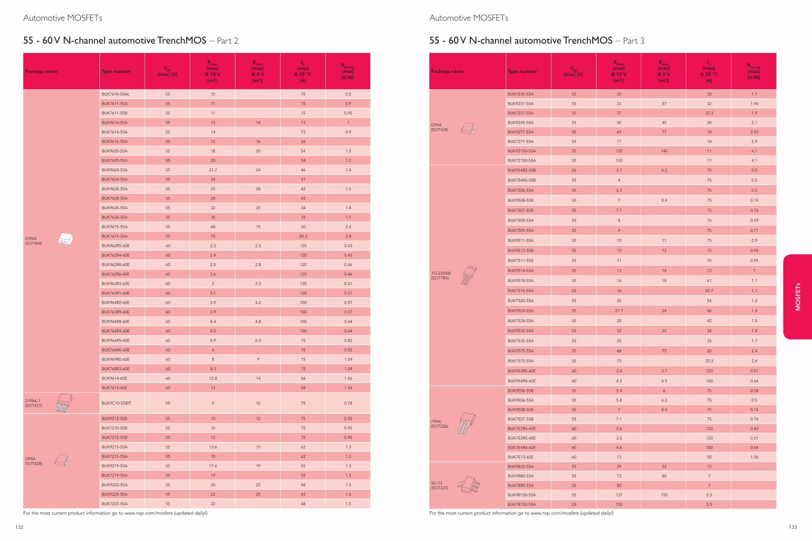
132 133
MO
SFE
Ts
For the most current product information go to www.nxp.com/mosfets (updated daily!) For the most current product information go to www.nxp.com/mosfets (updated daily!)
Package name Type numberVDS
[max] [V]
RDSon [max]
@ 10 V [mΩ]
RDSon [max] @ 5 V [mΩ]
ID [max]
@ 25 °C [A]
Rth(j-mb) [max] [K/W]
DPAK (SOT428)
BUK7230-55A 55 30 38 1.7
BUK9237-55A 55 33 37 32 1.94
BUK7237-55A 55 37 32.3 1.9
BUK9245-55A 55 40 45 28 2.1
BUK9277-55A 55 69 77 18 2.93
BUK7277-55A 55 77 18 2.9
BUK92150-55A 55 125 140 11 4.1
BUK72150-55A 55 150 11 4.1
TO-220AB (SOT78A)
BUK954R2-55B 55 3.7 4.2 75 0.5
BUK754R0-55B 55 4 75 0.5
BUK7506-55A 55 6.3 75 0.5
BUK9508-55B 55 7 8.4 75 0.74
BUK7507-55B 55 7.1 75 0.74
BUK7508-55A 55 8 75 0.59
BUK7509-55A 55 9 75 0.71
BUK9511-55A 55 10 11 75 0.9
BUK9512-55B 55 10 12 75 0.95
BUK7511-55B 55 11 75 0.95
BUK9514-55A 55 13 14 73 1
BUK9518-55A 55 16 18 61 1.1
BUK7516-55A 55 16 65.7 1.1
BUK7520-55A 55 20 54 1.2
BUK9524-55A 55 21.7 24 46 1.4
BUK7528-55A 55 28 42 1.5
BUK9535-55A 55 32 35 34 1.8
BUK7535-55A 55 35 35 1.7
BUK9575-55A 55 68 75 20 2.4
BUK7575-55A 55 75 20.3 2.4
BUK953R5-60E 60 3.4 3.7 120 0.51
BUK954R8-60E 60 4.5 4.9 100 0.64
I2PAK (SOT226)
BUK9E06-55B 55 5.4 6 75 0.58
BUK9E06-55A 55 5.8 6.3 75 0.5
BUK9E08-55B 55 7 8.4 75 0.74
BUK7E07-55B 55 7.1 75 0.74
BUK7E2R6-60E 60 2.6 120 0.43
BUK7E3R5-60E 60 3.5 120 0.51
BUK7E4R6-60E 60 4.6 100 0.64
BUK7E13-60E 60 13 58 1.56
SC-73 (SOT223)
BUK9832-55A 55 29 32 12
BUK9880-55A 55 73 80 7
BUK7880-55A 55 80 7
BUK98150-55A 55 137 150 5.5
BUK78150-55A 55 150 5.5
Package name Type numberVDS
[max] [V]
RDSon [max]
@ 10 V [mΩ]
RDSon [max] @ 5 V [mΩ]
ID [max]
@ 25 °C [A]
Rth(j-mb) [max] [K/W]
D2PAK (SOT404)
BUK7610-55AL 55 10 75 0.5
BUK7611-55A 55 11 75 0.9
BUK7611-55B 55 11 75 0.95
BUK9614-55A 55 13 14 73 1
BUK7614-55A 55 14 73 0.9
BUK9616-55A 55 15 16 66
BUK9620-55A 55 18 20 54 1.2
BUK7620-55A 55 20 54 1.2
BUK9624-55A 55 21.7 24 46 1.4
BUK7624-55A 55 24 47
BUK9628-55A 55 25 28 42 1.5
BUK7628-55A 55 28 42
BUK9635-55A 55 32 35 34 1.8
BUK7635-55A 55 35 35 1.7
BUK9675-55A 55 68 75 20 2.4
BUK7675-55A 55 75 20.3 2.4
BUK962R5-60E 60 2.3 2.5 120 0.43
BUK762R4-60E 60 2.4 120 0.43
BUK962R8-60E 60 2.5 2.8 120 0.46
BUK762R6-60E 60 2.6 120 0.46
BUK963R3-60E 60 3 3.3 120 0.51
BUK763R1-60E 60 3.1 120 0.51
BUK964R2-60E 60 3.9 4.2 100 0.57
BUK763R9-60E 60 3.9 100 0.57
BUK964R8-60E 60 4.4 4.8 100 0.64
BUK764R4-60E 60 4.5 100 0.64
BUK966R5-60E 60 5.9 6.5 75 0.82
BUK766R0-60E 60 6 75 0.82
BUK969R0-60E 60 8 9 75 1.09
BUK768R3-60E 60 8.3 75 1.09
BUK9614-60E 60 12.8 14 56 1.56
BUK7613-60E 60 13 58 1.56
D2PAK-7 (SOT427) BUK9C10-55BIT 55 9 10 75 0.78
DPAK (SOT428)
BUK9212-55B 55 10 12 75 0.95
BUK7210-55B 55 10 75 0.95
BUK7212-55B 55 12 75 0.95
BUK9215-55A 55 13.6 15 62 1.3
BUK7215-55A 55 15 62 1.3
BUK9219-55A 55 17.6 19 55 1.3
BUK7219-55A 55 19 55 1.3
BUK9222-55A 55 20 22 48 1.5
BUK9225-55A 55 22 25 43 1.6
BUK7222-55A 55 22 48 1.5
Automotive MOSFETs
55 - 60 V N-channel automotive TrenchMOS – Part 3
Automotive MOSFETs
55 - 60 V N-channel automotive TrenchMOS – Part 2
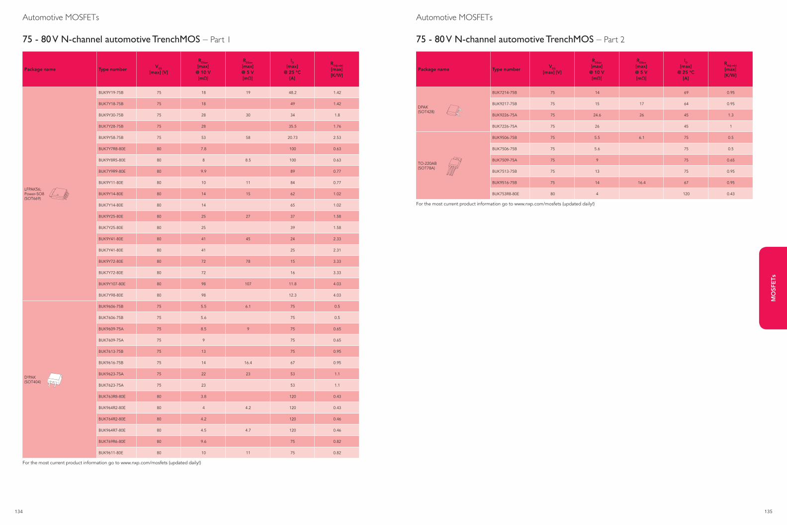
134 135
MO
SFE
Ts
For the most current product information go to www.nxp.com/mosfets (updated daily!)
Package name Type numberVDS
[max] [V]
RDSon [max]
@ 10 V [mΩ]
RDSon [max] @ 5 V [mΩ]
ID [max]
@ 25 °C [A]
Rth(j-mb) [max] [K/W]
DPAK (SOT428)
BUK7214-75B 75 14 69 0.95
BUK9217-75B 75 15 17 64 0.95
BUK9226-75A 75 24.6 26 45 1.3
BUK7226-75A 75 26 45 1
TO-220AB (SOT78A)
BUK9506-75B 75 5.5 6.1 75 0.5
BUK7506-75B 75 5.6 75 0.5
BUK7509-75A 75 9 75 0.65
BUK7513-75B 75 13 75 0.95
BUK9516-75B 75 14 16.4 67 0.95
BUK753R8-80E 80 4 120 0.43
Package name Type numberVDS
[max] [V]
RDSon [max]
@ 10 V [mΩ]
RDSon [max] @ 5 V [mΩ]
ID [max]
@ 25 °C [A]
Rth(j-mb) [max] [K/W]
LFPAK56; Power-SO8 (SOT669)
BUK9Y19-75B 75 18 19 48.2 1.42
BUK7Y18-75B 75 18 49 1.42
BUK9Y30-75B 75 28 30 34 1.8
BUK7Y28-75B 75 28 35.5 1.76
BUK9Y58-75B 75 53 58 20.73 2.53
BUK7Y7R8-80E 80 7.8 100 0.63
BUK9Y8R5-80E 80 8 8.5 100 0.63
BUK7Y9R9-80E 80 9.9 89 0.77
BUK9Y11-80E 80 10 11 84 0.77
BUK9Y14-80E 80 14 15 62 1.02
BUK7Y14-80E 80 14 65 1.02
BUK9Y25-80E 80 25 27 37 1.58
BUK7Y25-80E 80 25 39 1.58
BUK9Y41-80E 80 41 45 24 2.33
BUK7Y41-80E 80 41 25 2.31
BUK9Y72-80E 80 72 78 15 3.33
BUK7Y72-80E 80 72 16 3.33
BUK9Y107-80E 80 98 107 11.8 4.03
BUK7Y98-80E 80 98 12.3 4.03
D2PAK (SOT404)
BUK9606-75B 75 5.5 6.1 75 0.5
BUK7606-75B 75 5.6 75 0.5
BUK9609-75A 75 8.5 9 75 0.65
BUK7609-75A 75 9 75 0.65
BUK7613-75B 75 13 75 0.95
BUK9616-75B 75 14 16.4 67 0.95
BUK9623-75A 75 22 23 53 1.1
BUK7623-75A 75 23 53 1.1
BUK763R8-80E 80 3.8 120 0.43
BUK964R2-80E 80 4 4.2 120 0.43
BUK764R2-80E 80 4.2 120 0.46
BUK964R7-80E 80 4.5 4.7 120 0.46
BUK769R6-80E 80 9.6 75 0.82
BUK9611-80E 80 10 11 75 0.82
Automotive MOSFETs
75 - 80 V N-channel automotive TrenchMOS – Part 1
Automotive MOSFETs
75 - 80 V N-channel automotive TrenchMOS – Part 2
For the most current product information go to www.nxp.com/mosfets (updated daily!)
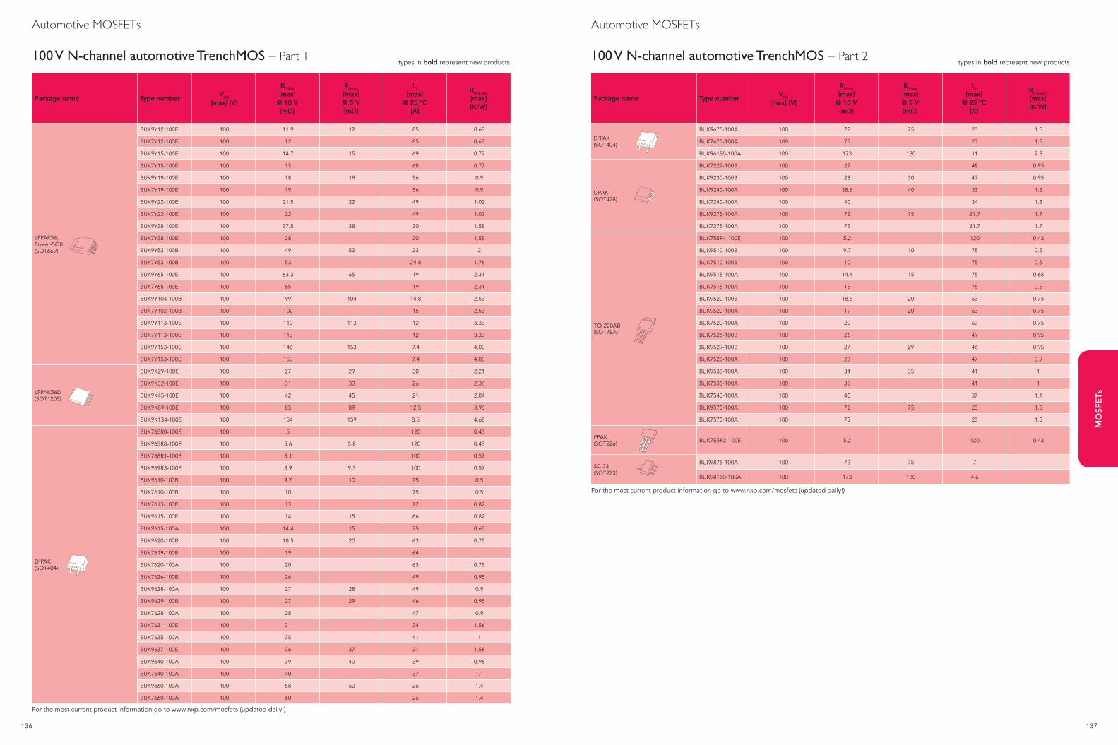
136 137
MO
SFE
Ts
Package name Type numberVDS
[max] [V]
RDSon [max]
@ 10 V [mΩ]
RDSon [max] @ 5 V [mΩ]
ID [max]
@ 25 °C [A]
Rth(j-mb) [max] [K/W]
D2PAK (SOT404)
BUK9675-100A 100 72 75 23 1.5
BUK7675-100A 100 75 23 1.5
BUK96180-100A 100 173 180 11 2.8
DPAK(SOT428)
BUK7227-100B 100 27 48 0.95
BUK9230-100B 100 28 30 47 0.95
BUK9240-100A 100 38.6 40 33 1.3
BUK7240-100A 100 40 34 1.3
BUK9275-100A 100 72 75 21.7 1.7
BUK7275-100A 100 75 21.7 1.7
TO-220AB (SOT78A)
BUK755R4-100E 100 5.2 120 0.43
BUK9510-100B 100 9.7 10 75 0.5
BUK7510-100B 100 10 75 0.5
BUK9515-100A 100 14.4 15 75 0.65
BUK7515-100A 100 15 75 0.5
BUK9520-100B 100 18.5 20 63 0.75
BUK9520-100A 100 19 20 63 0.75
BUK7520-100A 100 20 63 0.75
BUK7526-100B 100 26 49 0.95
BUK9529-100B 100 27 29 46 0.95
BUK7528-100A 100 28 47 0.9
BUK9535-100A 100 34 35 41 1
BUK7535-100A 100 35 41 1
BUK7540-100A 100 40 37 1.1
BUK9575-100A 100 72 75 23 1.5
BUK7575-100A 100 75 23 1.5
I2PAK (SOT226) BUK7E5R2-100E 100 5.2 120 0.43
SC-73 (SOT223)
BUK9875-100A 100 72 75 7
BUK98180-100A 100 173 180 4.6
For the most current product information go to www.nxp.com/mosfets (updated daily!)
For the most current product information go to www.nxp.com/mosfets (updated daily!)
Automotive MOSFETs
100 V N-channel automotive TrenchMOS – Part 1
Package name Type numberVDS
[max] [V]
RDSon [max]
@ 10 V [mΩ]
RDSon [max] @ 5 V [mΩ]
ID [max]
@ 25 °C [A]
Rth(j-mb) [max] [K/W]
LFPAK56; Power-SO8 (SOT669)
BUK9Y12-100E 100 11.9 12 85 0.63
BUK7Y12-100E 100 12 85 0.63
BUK9Y15-100E 100 14.7 15 69 0.77
BUK7Y15-100E 100 15 68 0.77
BUK9Y19-100E 100 18 19 56 0.9
BUK7Y19-100E 100 19 56 0.9
BUK9Y22-100E 100 21.5 22 49 1.02
BUK7Y22-100E 100 22 49 1.02
BUK9Y38-100E 100 37.5 38 30 1.58
BUK7Y38-100E 100 38 30 1.58
BUK9Y53-100B 100 49 53 23 2
BUK7Y53-100B 100 53 24.8 1.76
BUK9Y65-100E 100 63.3 65 19 2.31
BUK7Y65-100E 100 65 19 2.31
BUK9Y104-100B 100 99 104 14.8 2.53
BUK7Y102-100B 100 102 15 2.53
BUK9Y113-100E 100 110 113 12 3.33
BUK7Y113-100E 100 113 12 3.33
BUK9Y153-100E 100 146 153 9.4 4.03
BUK7Y153-100E 100 153 9.4 4.03
LFPAK56D (SOT1205)
BUK9K29-100E 100 27 29 30 2.21
BUK9K32-100E 100 31 33 26 2.36
BUK9K45-100E 100 42 45 21 2.84
BUK9K89-100E 100 85 89 12.5 3.96
BUK9K134-100E 100 154 159 8.5 4.68
D2PAK (SOT404)
BUK765R0-100E 100 5 120 0.43
BUK965R8-100E 100 5.6 5.8 120 0.43
BUK768R1-100E 100 8.1 100 0.57
BUK969R3-100E 100 8.9 9.3 100 0.57
BUK9610-100B 100 9.7 10 75 0.5
BUK7610-100B 100 10 75 0.5
BUK7613-100E 100 13 72 0.82
BUK9615-100E 100 14 15 66 0.82
BUK9615-100A 100 14.4 15 75 0.65
BUK9620-100B 100 18.5 20 63 0.75
BUK7619-100B 100 19 64
BUK7620-100A 100 20 63 0.75
BUK7626-100B 100 26 49 0.95
BUK9628-100A 100 27 28 49 0.9
BUK9629-100B 100 27 29 46 0.95
BUK7628-100A 100 28 47 0.9
BUK7631-100E 100 31 34 1.56
BUK7635-100A 100 35 41 1
BUK9637-100E 100 36 37 31 1.56
BUK9640-100A 100 39 40 39 0.95
BUK7640-100A 100 40 37 1.1
BUK9660-100A 100 58 60 26 1.4
BUK7660-100A 100 60 26 1.4
types in bold represent new products
Automotive MOSFETs
100 V N-channel automotive TrenchMOS – Part 2 types in bold represent new products
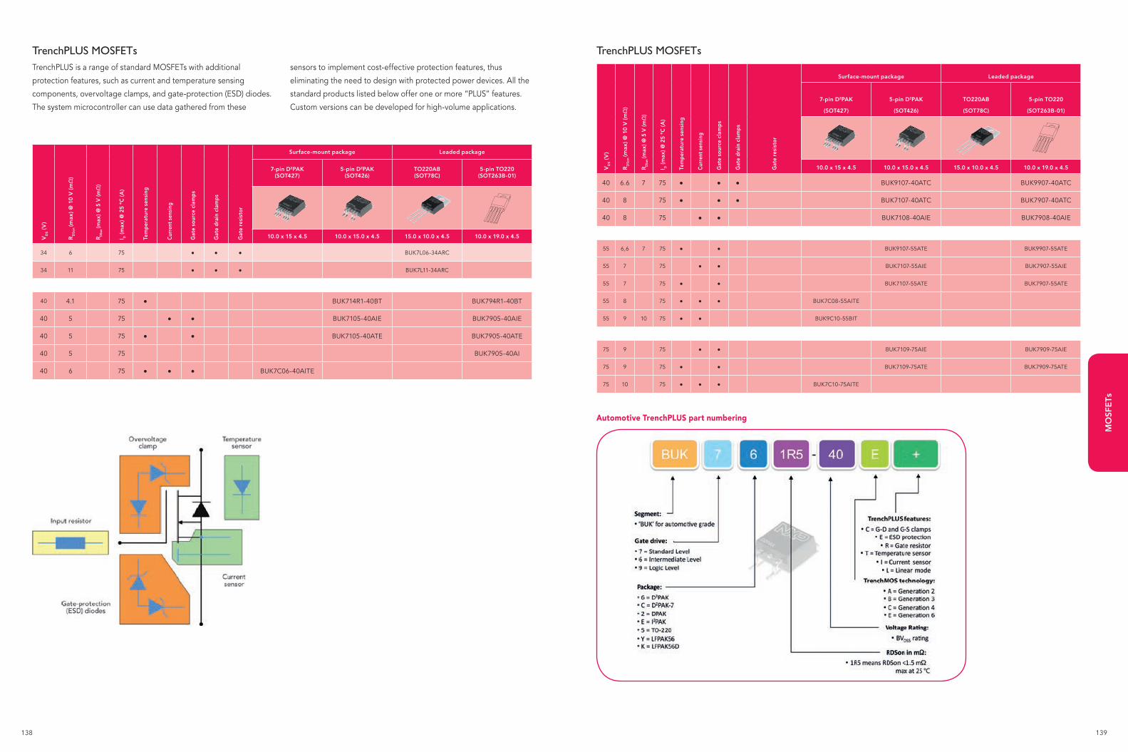
138 139
MO
SFE
Ts
TrenchPLUS MOSFETs
VD
S (V
)
RD
So
n (m
ax) @
10
V (
mΩ
)
R DSo
n (m
ax) @
5 V
(mΩ
)
I D (m
ax) @
25
°C (A
)
Tem
pera
ture
sen
sing
Cur
rent
sen
sing
Gat
e so
urce
cla
mps
Gat
e dr
ain
clam
ps
Gat
e re
sist
or
Surface-mount package Leaded package
7-pin D2PAK
(SOT427)
5-pin D2PAK
(SOT426)
TO220AB
(SOT78C)
5-pin TO220
(SOT263B-01)
10.0 x 15 x 4.5 10.0 x 15.0 x 4.5 15.0 x 10.0 x 4.5 10.0 x 19.0 x 4.5
40 6.6 7 75 BUK9107-40ATC BUK9907-40ATC
40 8 75 BUK7107-40ATC BUK7907-40ATC
40 8 75 BUK7108-40AIE BUK7908-40AIE
55 6,6 7 75 BUK9107-55ATE BUK9907-55ATE
55 7 75 BUK7107-55AIE BUK7907-55AIE
55 7 75 BUK7107-55ATE BUK7907-55ATE
55 8 75 BUK7C08-55AITE
55 9 10 75 BUK9C10-55BIT
75 9 75 BUK7109-75AIE BUK7909-75AIE
75 9 75 BUK7109-75ATE BUK7909-75ATE
75 10 75 BUK7C10-75AITE
Automotive TrenchPLUS part numbering
TrenchPLUS MOSFETsTrenchPLUS is a range of standard MOSFETs with additional
protection features, such as current and temperature sensing
components, overvoltage clamps, and gate-protection (ESD) diodes.
The system microcontroller can use data gathered from these
sensors to implement cost-effective protection features, thus
eliminating the need to design with protected power devices. All the
standard products listed below offer one or more “PLUS” features.
Custom versions can be developed for high-volume applications.
VD
S (V
)
RD
So
n (m
ax) @
10
V (
mΩ
)
R DSo
n (m
ax) @
5 V
(mΩ
)
I D (m
ax) @
25
°C (A
)
Tem
pera
ture
sen
sing
Cur
rent
sen
sing
Gat
e so
urce
cla
mps
Gat
e dr
ain
clam
ps
Gat
e re
sist
or
Surface-mount package Leaded package
7-pin D2PAK(SOT427)
5-pin D2PAK(SOT426)
TO220AB(SOT78C)
5-pin TO220(SOT263B-01)
10.0 x 15 x 4.5 10.0 x 15.0 x 4.5 15.0 x 10.0 x 4.5 10.0 x 19.0 x 4.5
34 6 75 BUK7L06-34ARC
34 11 75 BUK7L11-34ARC
40 4.1 75 BUK714R1-40BT BUK794R1-40BT
40 5 75 BUK7105-40AIE BUK7905-40AIE
40 5 75 BUK7105-40ATE BUK7905-40ATE
40 5 75 BUK7905-40AI
40 6 75 BUK7C06-40AITE

141
Thyristors
AC Thyristor Triacs / AC Thyristors / TOPTriacs 142AC Thyristor Triacs 142AC Thyristors 142
Temperature and Overload Protected Triacs (TOPTriacs) 142
3-quadrant Hi-Com 143
4-quadrant triacs 144
Silicon Controlled Rectifiers 145
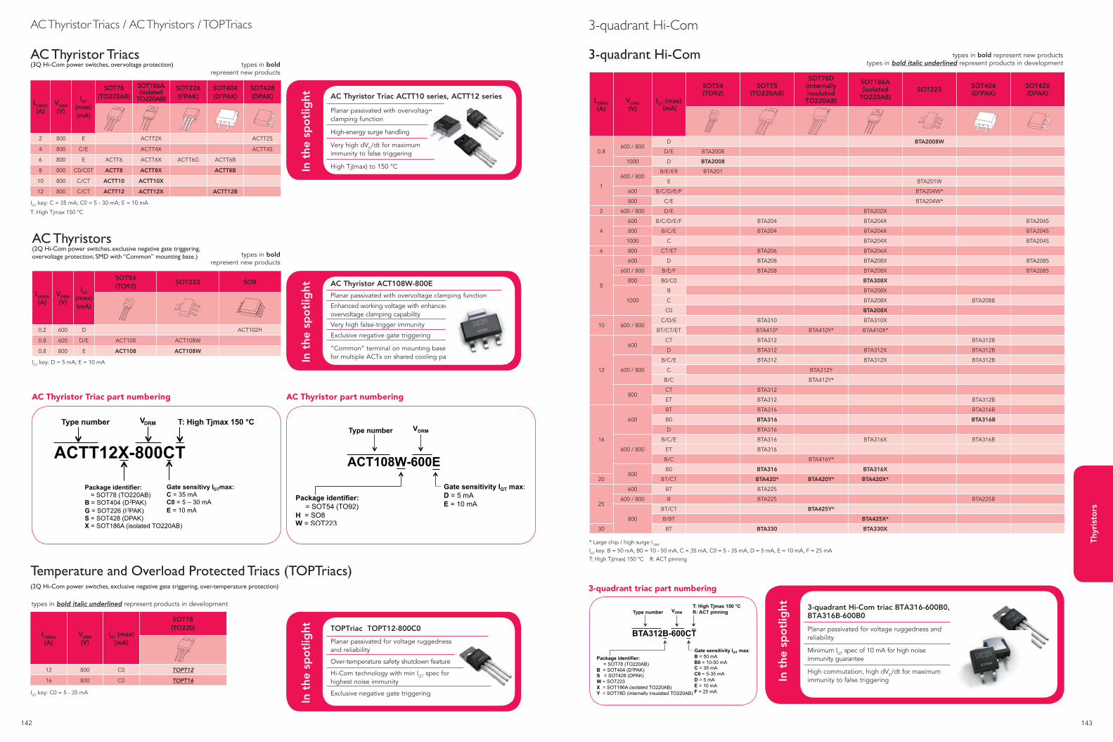
142 143
Thyr
isto
rs
IT(RMS)
(A)VDRM
(V)IGT (max)
(mA)
SOT54(TO92)
SOT78(TO220AB)
SOT78D(internally insulated
TO220AB)
SOT186A(isolated
TO220AB)SOT223 SOT404
(D2PAK)SOT428(DPAK)
0.8600 / 800
D BTA2008W
D/E BTA2008
1000 D BTA2008
1
600 / 800B/E/ER BTA201
E BTA201W
600 B/C/D/E/F BTA204W*
800 C/E BTA204W*
2 600 / 800 D/E BTA202X
4
600 B/C/D/E/F BTA204 BTA204X BTA204S
800 B/C/E BTA204 BTA204X BTA204S
1000 C BTA204X BTA204S
6 800 CT/ET BTA206 BTA206X
8
600 D BTA208 BTA208X BTA208S
600 / 800 B/E/F BTA208 BTA208X BTA208S
800 B0/C0 BTA308X
1000
B BTA208X
C BTA208X BTA208B
C0 BTA208X
10 600 / 800C/D/E BTA310 BTA310X
BT/CT/ET BTA410* BTA410Y* BTA410X*
12
600CT BTA312 BTA312B
D BTA312 BTA312X BTA312B
600 / 800
B/C/E BTA312 BTA312X BTA312B
C BTA312Y
B/C BTA412Y*
800CT BTA312
ET BTA312 BTA312B
16
600
BT BTA316 BTA316B
B0 BTA316 BTA316B
D BTA316
600 / 800
B/C/E BTA316 BTA316X BTA316B
ET BTA316
B/C BTA416Y*
800B0 BTA316 BTA316X
20 BT/CT BTA420* BTA420Y* BTA420X*
25
600 BT BTA225
600 / 800 B BTA225 BTA225B
800
BT/CT BTA425Y*
B/BT BTA425X*
30 BT BTA330 BTA330X
3-quadrant Hi-Com types in bold represent new productstypes in bold italic underlined represent products in development
* Large chip / high surge ITSM
IGT key: B = 50 mA, B0 = 10 - 50 mA, C = 35 mA, C0 = 5 - 35 mA, D = 5 mA, E = 10 mA, F = 25 mAT: High Tj(max) 150 °C R: ACT pinning
3-quadrant Hi-Com triac BTA316-600B0, BTA316B-600B0
Planar passivated for voltage ruggedness and reliability
Minimum IGT spec of 10 mA for high noise immunity guarantee
High commutation, high dVD/dt for maximum immunity to false triggeringIn
the
sp
otl
ight
3-quadrant triac part numbering
3-quadrant Hi-ComAC Thyristor Triacs / AC Thyristors / TOPTriacs
Temperature and Overload Protected Triacs (TOPTriacs)(2Q Hi-Com power switches, exclusive negative gate triggering, over-temperature protection)
types in bold italic underlined represent products in development
IT(RMS)
(A)VDRM
(V)IGT (max)
(mA)
SOT78(TO220)
12 800 C0 TOPT12
16 800 C0 TOPT16
IGT key: C0 = 5 - 35 mA
AC Thyristor Triacs (3Q Hi-Com power switches, overvoltage protection) types in bold
represent new products
IT(RMS)
(A)VDRM
(V)
IGT (max)(mA)
SOT78(TO220AB)
SOT186A(isolated
TO220AB)
SOT226(I2PAK)
SOT404(D2PAK)
SOT428(DPAK)
2 800 E ACTT2X ACTT2S
4 800 C/E ACTT4X ACTT4S
6 800 E ACTT6 ACTT6X ACTT6G ACTT6B
8 800 C0/C0T ACTT8 ACTT8X ACTT8B
10 800 C/CT ACTT10 ACTT10X
12 800 C/CT ACTT12 ACTT12X ACTT12B
IGT key: C = 35 mA; C0 = 5 - 30 mA; E = 10 mA
T: High Tjmax 150 °C
AC Thyristor part numberingAC Thyristor Triac part numbering
ACTT12X-800CT
Type number VDRM T: High Tjmax 150 °C
Package identifier: = SOT78 (TO220AB) B = SOT404 (D2PAK) G = SOT226 (I2PAK) S = SOT428 (DPAK) X = SOT186A (isolated TO220AB)
Gate sensitivy IGT max: C = 35 mA C0 = 5 – 30 mA E = 10 mA
AC Thyristors (2Q Hi-Com power switches, exclusive negative gate triggering, overvoltage protection; SMD with “Common” mounting base.)
AC Thyristor Triac ACTT10 series, ACTT12 series
Planar passivated with overvoltage clamping function
High-energy surge handling
Very high dVD/dt for maximum immunity to false triggering
High Tj(max) to 150 °CIn t
he s
po
tlig
ht
TOPTriac TOPT12-800C0
Planar passivated for voltage ruggednessand reliability
Over-temperature safety shutdown feature
Hi-Com technology with min IGT spec for highest noise immunity
Exclusive negative gate triggering
In t
he s
po
tlig
htIT(RMS) (A)
VDRM (V)
IGT (max) (mA)
SOT54(TO92)
SOT223 SO8
0.2 600 D ACT102H
0.8 600 D/E ACT108 ACT108W
0.8 800 E ACT108 ACT108W
types in bold represent new products
IGT key: D = 5 mA; E = 10 mA In t
he s
po
tlig
ht AC Thyristor ACT108W-800E
Planar passivated with overvoltage clamping function
Enhanced working voltage with enhanced overvoltage clamping capability
Very high false-trigger immunity
Exclusive negative gate triggering
“Common” terminal on mounting base for multiple ACTs on shared cooling pad
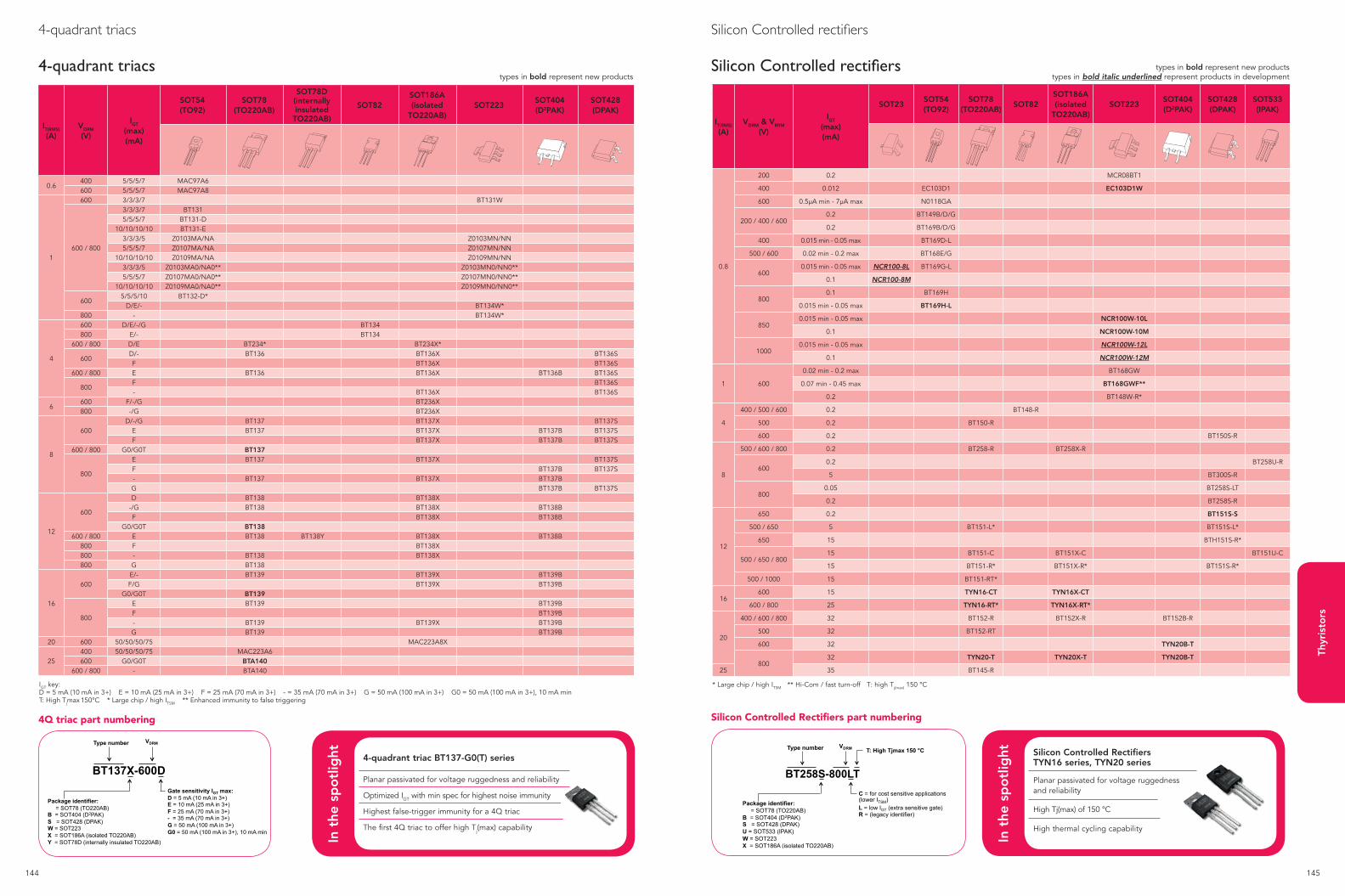
144 145
Thyr
isto
rs
Silicon Controlled Rectifiers part numbering
Silicon Controlled Rectifiers TYN16 series, TYN20 series
Planar passivated for voltage ruggedness and reliability
High Tj(max) of 150 °C
High thermal cycling capability
In t
he s
po
tlig
ht
Silicon Controlled rectifiers
Silicon Controlled rectifiers
* Large chip / high ITSM ** Hi-Com / fast turn-off T: high Tj(max) 150 °C
BT258S-800LT
(lower ITSM)
IGT key:D = 5 mA (10 mA in 3+) E = 10 mA (25 mA in 3+) F = 25 mA (70 mA in 3+) - = 35 mA (70 mA in 3+) G = 50 mA (100 mA in 3+) G0 = 50 mA (100 mA in 3+), 10 mA minT: High Tjmax 150°C * Large chip / high ITSM ** Enhanced immunity to false triggering
4-quadrant triac BT137-G0(T) series
Planar passivated for voltage ruggedness and reliability
Optimized IGT with min spec for highest noise immunity
Highest false-trigger immunity for a 4Q triac
The first 4Q triac to offer high Tj(max) capability
In t
he s
po
tlig
ht
BT137X-600D
Type number VDRM
Package identifier: = SOT78 (TO220AB) B = SOT404 (D2PAK) S = SOT428 (DPAK) W = SOT223 X = SOT186A (isolated TO220AB) Y = SOT78D (internally insulated TO220AB)
Gate sensitivity IGT max: D = 5 mA (10 mA in 3+) E = 10 mA (25 mA in 3+) F = 25 mA (70 mA in 3+) - = 35 mA (70 mA in 3+) G = 50 mA (100 mA in 3+) G0 = 50 mA (100 mA in 3+), 10 mA min
4Q triac part numbering
4-quadrant triacs
4-quadrant triacs
IT(RMS) (A)
VDRM (V)
IGT (max) (mA)
SOT54(TO92)
SOT78(TO220AB)
SOT78D(internally insulated
TO220AB)
SOT82SOT186A(isolated
TO220AB)SOT223
SOT404(D2PAK)
SOT428(DPAK)
0.6400 5/5/5/7 MAC97A6600 5/5/5/7 MAC97A8
1
600 3/3/3/7 BT131W
600 / 800
3/3/3/7 BT1315/5/5/7 BT131-D
10/10/10/10 BT131-E3/3/3/5 Z0103MA/NA Z0103MN/NN5/5/5/7 Z0107MA/NA Z0107MN/NN
10/10/10/10 Z0109MA/NA Z0109MN/NN3/3/3/5 Z0103MA0/NA0** Z0103MN0/NN0**5/5/5/7 Z0107MA0/NA0** Z0107MN0/NN0**
10/10/10/10 Z0109MA0/NA0** Z0109MN0/NN0**
6005/5/5/10 BT132-D*
D/E/- BT134W*800 - BT134W*
4
600 D/E/-/G BT134800 E/- BT134
600 / 800 D/E BT234* BT234X*
600D/- BT136 BT136X BT136SF BT136X BT136S
600 / 800 E BT136 BT136X BT136B BT136S
800F BT136S- BT136X BT136S
6600 F/-/G BT236X800 -/G BT236X
8
600D/-/G BT137 BT137X BT137S
E BT137 BT137X BT137B BT137SF BT137X BT137B BT137S
600 / 800 G0/G0T BT137
800
E BT137 BT137X BT137SF BT137B BT137S- BT137 BT137X BT137BG BT137B BT137S
12
600
D BT138 BT138X-/G BT138 BT138X BT138BF BT138X BT138B
G0/G0T BT138600 / 800 E BT138 BT138Y BT138X BT138B
800 F BT138X800 - BT138 BT138X800 G BT138
16
600E/- BT139 BT139X BT139BF/G BT139X BT139B
G0/G0T BT139
800
E BT139 BT139BF BT139B- BT139 BT139X BT139BG BT139 BT139B
20 600 50/50/50/75 MAC223A8X
25400 50/50/50/75 MAC223A6600 G0/G0T BTA140
600 / 800 - BTA140
types in bold represent new productstypes in bold italic underlined represent products in developmenttypes in bold represent new products
IT(RMS) (A)
VDRM & VRRM (V)
IGT (max) (mA)
SOT23SOT54(TO92)
SOT78(TO220AB)
SOT82SOT186A(isolated
TO220AB)SOT223
SOT404(D2PAK)
SOT428(DPAK)
SOT533(IPAK)
0.8
200 0.2 MCR08BT1
400 0.012 EC103D1 EC103D1W
600 0.5μA min - 7μA max N0118GA
200 / 400 / 6000.2 BT149B/D/G
0.2 BT169B/D/G
400 0.015 min - 0.05 max BT169D-L
500 / 600 0.02 min - 0.2 max BT168E/G
6000.015 min - 0.05 max NCR100-8L BT169G-L
0.1 NCR100-8M
8000.1 BT169H
0.015 min - 0.05 max BT169H-L
8500.015 min - 0.05 max NCR100W-10L
0.1 NCR100W-10M
10000.015 min - 0.05 max NCR100W-12L
0.1 NCR100W-12M
1 600
0.02 min - 0.2 max BT168GW
0.07 min - 0.45 max BT168GWF**
0.2 BT148W-R*
4
400 / 500 / 600 0.2 BT148-R
500 0.2 BT150-R
600 0.2 BT150S-R
8
500 / 600 / 800 0.2 BT258-R BT258X-R
6000.2 BT258U-R
5 BT300S-R
8000.05 BT258S-LT
0.2 BT258S-R
12
650 0.2 BT151S-S
500 / 650 5 BT151-L* BT151S-L*
650 15 BTH151S-R*
500 / 650 / 80015 BT151-C BT151X-C BT151U-C
15 BT151-R* BT151X-R* BT151S-R*
500 / 1000 15 BT151-RT*
16600 15 TYN16-CT TYN16X-CT
600 / 800 25 TYN16-RT* TYN16X-RT*
20
400 / 600 / 800 32 BT152-R BT152X-R BT152B-R
500 32 BT152-RT
600 32 TYN20B-T
80032 TYN20-T TYN20X-T TYN20B-T
25 35 BT145-R
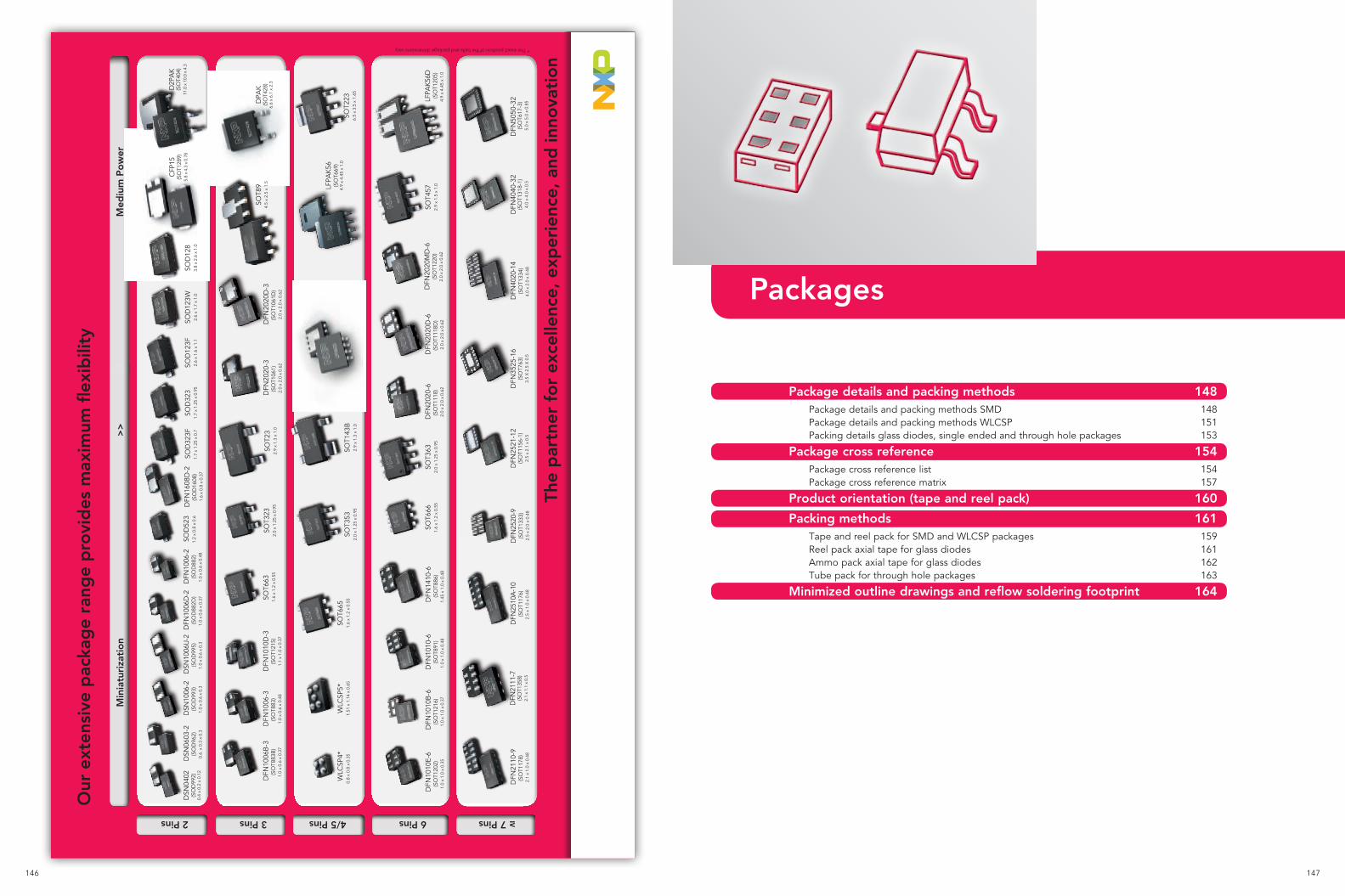
146 147
Min
iatu
rizat
ion
>>M
ediu
m P
ower
SOD
523
1.2
x 0.
8 x
0.6
DFN
1006
D-2
(SO
D88
2D)
1.0
x 0.
6 x
0.37
DFN
1006
-2(S
OD
882)
1.0
x 0.
6 x
0.48
CFP
15(S
OT1
289)
5.8
x 4.
3 x
0.78
D2P
AK
(SO
T404
)11
.0 x
10.
0 x
4.3
DFN
2111
-7(S
OT1
358)
2.1
x 1.
1 x
0.5
LFPA
K33
(SO
T121
0)3.
3 x
3.3
x 0.
85
DPA
K(S
OT4
28)
6.6
x 6.
1 x
2.3
DFN
1608
D-2
(SO
D16
08)
1.6
x 0.
8 x
0.37
DSN
0603
-2(S
OD
962)
0.6.
x 0
.3 x
0.3
DSN
0402
(SO
D99
2)0.
4 x
0.2
x 0.
12
SOT6
631.
6 x
1.2
x 0.
55
DFN
1006
-3(S
OT8
83)
1.0
x 0.
6 x
0.48
DFN
1010
D-3
(SO
T121
5)1.
1 x
1.0
x 0.
37
DFN
1006
B-3
(SO
T883
B)
1.0
x 0.
6 x
0.37
WLC
SP4*
0.8
x 0.
8 x
0.35
WLC
SP5*
1.51
x 1
.14
x 0.
65
SOT6
651.
6 x
1.2
x 0.
55 DFN
1410
-6(S
OT8
86)
1.45
x 1
.0 x
0.4
8
DFN
1010
-6(S
OT8
91)
1.0
x 1.
0 x
0.48
DFN
1010
B-6
(SO
T121
6)1.
0 x
1.0
x 0.
37
DFN
1010
E-6
(SO
T120
2)1.
0 x
1.0
x 0.
35
SOT6
661.
6 x
1.2
x 0.
55
DFN
2020
-6(S
OT1
118)
2.0
x 2.
0 x
0.62
SOT1
43B
2.9
x 1.
3 x
1.0
SOD
123W
2.6
x 1.
7 x
1.0
DFN
2020
-3(S
OT1
061)
2.0
x 2.
0 x
0.62
DFN
2020
D-3
(SO
T106
1D)
2.0
x 2.
0 x
0.62
SOT3
232.
0 x
1.25
x 0
.95
SOT3
532.
0 x
1.25
x 0
.95
DFN
2020
MD
-6(S
OT1
220)
2.0
x 2.
0 x
0.62
SOT3
632.
0 x
1.25
x 0
.95
SOD
128
3.8
x 2.
6 x
1.0
SOT8
94.
5 x
2.5
x 1.
5
SOT2
236.
5 x
3.5
x 1.
65
SOT2
32.
9 x
1.3
x 1.
0
SOT4
572.
9 x
1.5
x 1.
0
DFN
2110
-9(S
OT1
178)
2.1
x 1.
0 x
0.48
DFN
2521
-12
(SO
T115
6-1)
2.5
x 2.
1 x
0.5
DFN
4040
-32
(SO
T131
8-1)
4.0
x 4.
0 x
0.5
DFN
5050
-32
(SO
T617
-3)
5.0
x 5.
0 x
0.85
DFN
2510
A-1
0(S
OT1
176)
2.5
x 1.
0 x
0.48
LFPA
K56D
(SO
T120
5)4.
9 x
4.45
x 1
.0
DFN
2520
-9(S
OT1
333)
2.
5 x
2.0
x 0.
48
2 Pins 3 Pins 4/5 Pins 6 Pins ≥ 7 Pins
SOD
123F
2.6
x 1.
6 x
1.1
SOD
323
1.7
x 1.
25 x
0.9
5
SOD
323F
1.7
x 1.
25 x
0.7
LFPA
K56
(SO
T669
)4.
9 x
4.45
x 1
.0
DFN
4020
-14
(SO
T133
4)4.
0 x
2.0
x 0.
48
DFN
3525
-16
(SO
T763
)3.
5 X
2.5
X 0
.5
DFN
2020
D-6
(SO
T111
8D)
2.0
x 2.
0 x
0.62
DSN
1006
-2(S
OD
993)
1.0
x 0.
6 x
0.3
DSN
1006
U-2
(SO
D99
5)1.
0 x
0.6
x 0.
3
Our
ext
ensi
ve p
acka
ge
rang
e p
rovi
des
max
imum
flex
ibili
ty
The
par
tner
fo
r ex
celle
nce,
exp
erie
nce,
and
inno
vati
on
* The exact position of the balls and package dimensions vary.
Packages
Package details and packing methods 148Package details and packing methods SMD 148Package details and packing methods WLCSP 151Packing details glass diodes, single ended and through hole packages 153
Package cross reference 154Package cross reference list 154Package cross reference matrix 157
Product orientation (tape and reel pack) 160
Packing methods 161Tape and reel pack for SMD and WLCSP packages 159 Reel pack axial tape for glass diodes 161Ammo pack axial tape for glass diodes 162Tube pack for through hole packages 163
Minimized outline drawings and reflow soldering footprint 164
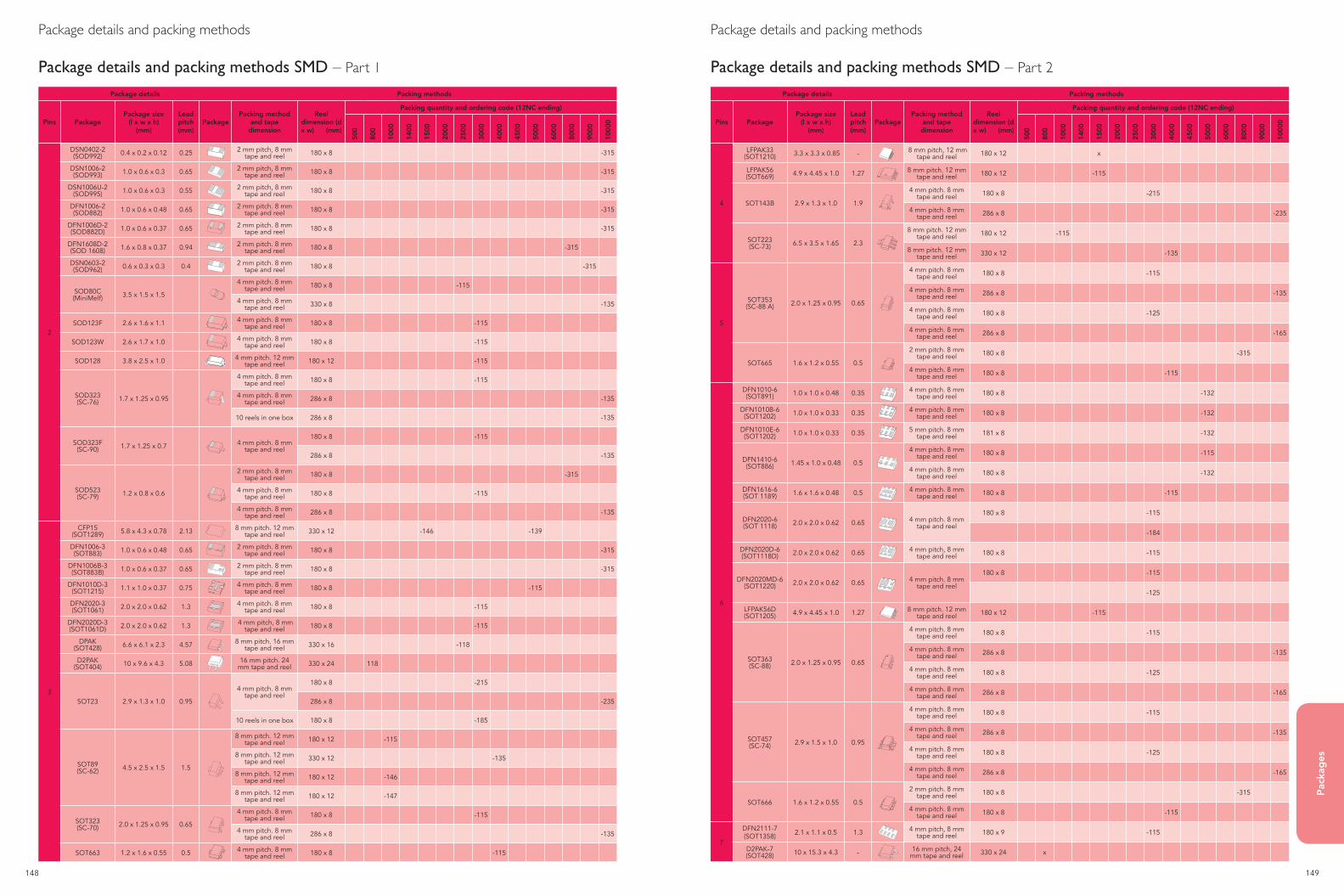
148 149
Pac
kag
es
Package details Packing methods
Pins PackagePackage size
(l x w x h) (mm)
Lead pitch(mm)
PackagePacking method
and tapedimension
Reeldimension (d x w) (mm)
Packing quantity and ordering code (12NC ending)
500
800
1000
1400
1500
2000
2500
3000
4000
4500
5000
6000
8000
9000
1000
0
4
LFPAK33 (SOT1210) 3.3 x 3.3 x 0.85 - 8 mm pitch, 12 mm
tape and reel 180 x 12 x
LFPAK56(SOT669) 4.9 x 4.45 x 1.0 1.27 8 mm pitch. 12 mm
tape and reel 180 x 12 -115
SOT143B 2.9 x 1.3 x 1.0 1.9
4 mm pitch. 8 mm tape and reel 180 x 8 -215
4 mm pitch. 8 mm tape and reel 286 x 8 -235
SOT223(SC-73) 6.5 x 3.5 x 1.65 2.3
8 mm pitch. 12 mm tape and reel 180 x 12 -115
8 mm pitch. 12 mm tape and reel 330 x 12 -135
5
SOT353 (SC-88 A) 2.0 x 1.25 x 0.95 0.65
4 mm pitch. 8 mm tape and reel 180 x 8 -115
4 mm pitch. 8 mm tape and reel 286 x 8 -135
4 mm pitch. 8 mm tape and reel 180 x 8 -125
4 mm pitch. 8 mm tape and reel 286 x 8 -165
SOT665 1.6 x 1.2 x 0.55 0.5
2 mm pitch. 8 mm tape and reel 180 x 8 -315
4 mm pitch. 8 mm tape and reel 180 x 8 -115
6
DFN1010-6 (SOT891) 1.0 x 1.0 x 0.48 0.35 4 mm pitch. 8 mm
tape and reel 180 x 8 -132
DFN1010B-6 (SOT1202) 1.0 x 1.0 x 0.33 0.35 4 mm pitch. 8 mm
tape and reel 180 x 8 -132
DFN1010E-6 (SOT1202) 1.0 x 1.0 x 0.33 0.35 5 mm pitch. 8 mm
tape and reel 181 x 8 -132
DFN1410-6 (SOT886) 1.45 x 1.0 x 0.48 0.5
4 mm pitch. 8 mm tape and reel 180 x 8 -115
4 mm pitch. 8 mm tape and reel 180 x 8 -132
DFN1616-6 (SOT 1189) 1.6 x 1.6 x 0.48 0.5 4 mm pitch. 8 mm
tape and reel 180 x 8 -115
DFN2020-6 (SOT 1118) 2.0 x 2.0 x 0.62 0.65 4 mm pitch. 8 mm
tape and reel
180 x 8 -115
-184
DFN2020D-6 (SOT1118D) 2.0 x 2.0 x 0.62 0.65 4 mm pitch, 8 mm
tape and reel 180 x 8 -115
DFN2020MD-6 (SOT1220) 2.0 x 2.0 x 0.62 0.65 4 mm pitch. 8 mm
tape and reel
180 x 8 -115
-125
LFPAK56D (SOT1205) 4.9 x 4.45 x 1.0 1.27 8 mm pitch. 12 mm
tape and reel 180 x 12 -115
SOT363 (SC-88) 2.0 x 1.25 x 0.95 0.65
4 mm pitch. 8 mm tape and reel 180 x 8 -115
4 mm pitch. 8 mm tape and reel 286 x 8 -135
4 mm pitch. 8 mm tape and reel 180 x 8 -125
4 mm pitch. 8 mm tape and reel 286 x 8 -165
SOT457 (SC-74) 2.9 x 1.5 x 1.0 0.95
4 mm pitch. 8 mm tape and reel 180 x 8 -115
4 mm pitch. 8 mm tape and reel 286 x 8 -135
4 mm pitch. 8 mm tape and reel 180 x 8 -125
4 mm pitch. 8 mm tape and reel 286 x 8 -165
SOT666 1.6 x 1.2 x 0.55 0.5
2 mm pitch. 8 mm tape and reel 180 x 8 -315
4 mm pitch. 8 mm tape and reel 180 x 8 -115
7
DFN2111-7 (SOT1358) 2.1 x 1.1 x 0.5 1.3 4 mm pitch, 8 mm
tape and reel 180 x 9 -115
D2PAK-7 (SOT428) 10 x 15.3 x 4.3 - 16 mm pitch, 24
mm tape and reel 330 x 24 x
Package details and packing methods
Package details and packing methods SMD – Part 2
Package details Packing methods
Pins PackagePackage size
(l x w x h) (mm)
Lead pitch(mm)
PackagePacking method
and tapedimension
Reeldimension (d x w) (mm)
Packing quantity and ordering code (12NC ending)
500
800
1000
1400
1500
2000
2500
3000
4000
4500
5000
6000
8000
9000
1000
0
2
DSN0402-2 (SOD992) 0.4 x 0.2 x 0.12 0.25 2 mm pitch, 8 mm
tape and reel 180 x 8 -315
DSN1006-2 (SOD993) 1.0 x 0.6 x 0.3 0.65 2 mm pitch, 8 mm
tape and reel 180 x 8 -315
DSN1006U-2 (SOD995) 1.0 x 0.6 x 0.3 0.55 2 mm pitch, 8 mm
tape and reel 180 x 8 -315
DFN1006-2 (SOD882) 1.0 x 0.6 x 0.48 0.65 2 mm pitch. 8 mm
tape and reel 180 x 8 -315
DFN1006D-2 (SOD882D) 1.0 x 0.6 x 0.37 0.65 2 mm pitch. 8 mm
tape and reel 180 x 8 -315
DFN1608D-2 (SOD 1608) 1.6 x 0.8 x 0.37 0.94 2 mm pitch. 8 mm
tape and reel 180 x 8 -315
DSN0603-2 (SOD962) 0.6 x 0.3 x 0.3 0.4 2 mm pitch. 8 mm
tape and reel 180 x 8 -315
SOD80C (MiniMelf) 3.5 x 1.5 x 1.5
4 mm pitch. 8 mm tape and reel 180 x 8 -115
4 mm pitch. 8 mm tape and reel 330 x 8 -135
SOD123F 2.6 x 1.6 x 1.1 4 mm pitch. 8 mm tape and reel 180 x 8 -115
SOD123W 2.6 x 1.7 x 1.0 4 mm pitch. 8 mm tape and reel 180 x 8 -115
SOD128 3.8 x 2.5 x 1.0 4 mm pitch. 12 mm tape and reel 180 x 12 -115
SOD323 (SC-76) 1.7 x 1.25 x 0.95
4 mm pitch. 8 mm tape and reel 180 x 8 -115
4 mm pitch. 8 mm tape and reel 286 x 8 -135
10 reels in one box 286 x 8 -135
SOD323F (SC-90) 1.7 x 1.25 x 0.7 4 mm pitch. 8 mm
tape and reel
180 x 8 -115
286 x 8 -135
SOD523 (SC-79) 1.2 x 0.8 x 0.6
2 mm pitch. 8 mm tape and reel 180 x 8 -315
4 mm pitch. 8 mm tape and reel 180 x 8 -115
4 mm pitch. 8 mm tape and reel 286 x 8 -135
3
CFP15 (SOT1289) 5.8 x 4.3 x 0.78 2.13 8 mm pitch. 12 mm
tape and reel 330 x 12 -146 -139
DFN1006-3 (SOT883) 1.0 x 0.6 x 0.48 0.65 2 mm pitch. 8 mm
tape and reel 180 x 8 -315
DFN1006B-3 (SOT883B) 1.0 x 0.6 x 0.37 0.65 2 mm pitch. 8 mm
tape and reel 180 x 8 -315
DFN1010D-3 (SOT1215) 1.1 x 1.0 x 0.37 0.75 4 mm pitch. 8 mm
tape and reel 180 x 8 -115
DFN2020-3 (SOT1061) 2.0 x 2.0 x 0.62 1.3 4 mm pitch. 8 mm
tape and reel 180 x 8 -115
DFN2020D-3 (SOT1061D) 2.0 x 2.0 x 0.62 1.3 4 mm pitch, 8 mm
tape and reel 180 x 8 -115
DPAK(SOT428) 6.6 x 6.1 x 2.3 4.57 8 mm pitch. 16 mm
tape and reel 330 x 16 -118
D2PAK(SOT404) 10 x 9.6 x 4.3 5.08 16 mm pitch. 24
mm tape and reel 330 x 24 118
SOT23 2.9 x 1.3 x 1.0 0.95
4 mm pitch. 8 mm tape and reel
180 x 8 -215
286 x 8 -235
10 reels in one box 180 x 8 -185
SOT89(SC-62) 4.5 x 2.5 x 1.5 1.5
8 mm pitch. 12 mm tape and reel 180 x 12 -115
8 mm pitch. 12 mm tape and reel 330 x 12 -135
8 mm pitch. 12 mm tape and reel 180 x 12 -146
8 mm pitch. 12 mm tape and reel 180 x 12 -147
SOT323(SC-70) 2.0 x 1.25 x 0.95 0.65
4 mm pitch. 8 mm tape and reel 180 x 8 -115
4 mm pitch. 8 mm tape and reel 286 x 8 -135
SOT663 1.2 x 1.6 x 0.55 0.5 4 mm pitch. 8 mm tape and reel 180 x 8 -115
Package details and packing methods
Package details and packing methods SMD – Part 1
M3D109
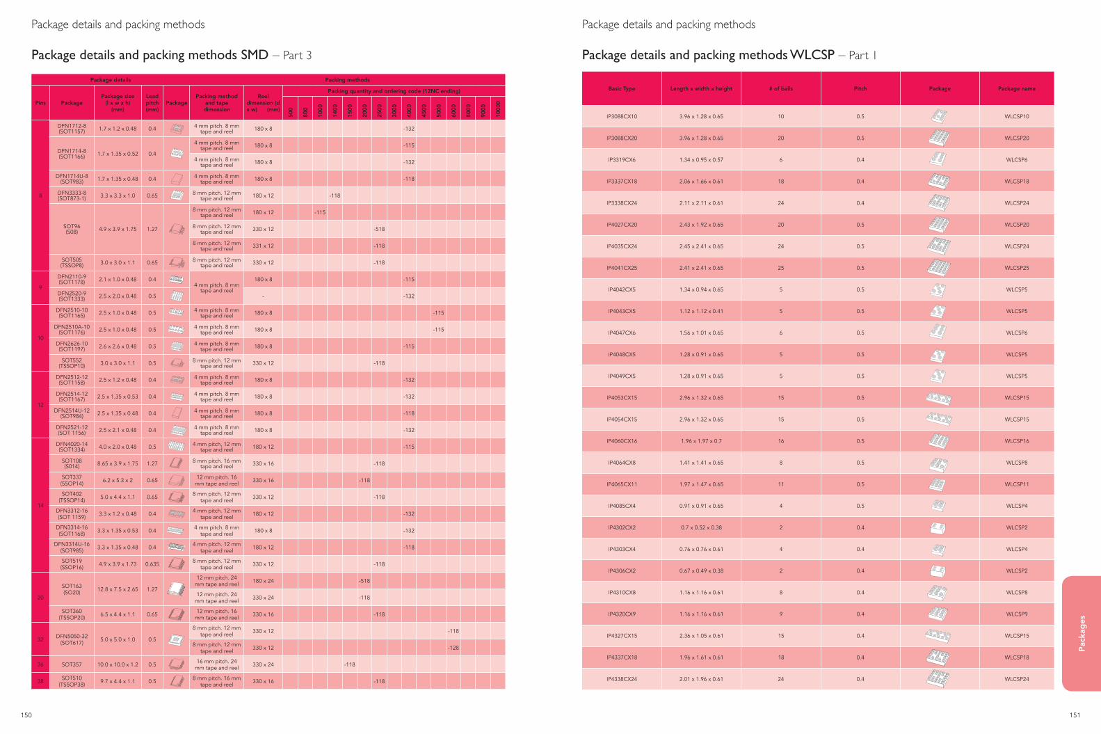
150 151
Pac
kag
es
Package details Packing methods
Pins PackagePackage size
(l x w x h) (mm)
Lead pitch(mm)
PackagePacking method
and tapedimension
Reeldimension (d x w) (mm)
Packing quantity and ordering code (12NC ending)
500
800
1000
1400
1500
2000
2500
3000
4000
4500
5000
6000
8000
9000
1000
0
8
DFN1712-8 (SOT1157) 1.7 x 1.2 x 0.48 0.4 4 mm pitch. 8 mm
tape and reel 180 x 8 -132
DFN1714-8 (SOT1166) 1.7 x 1.35 x 0.52 0.4
4 mm pitch. 8 mm tape and reel 180 x 8 -115
4 mm pitch. 8 mm tape and reel 180 x 8 -132
DFN1714U-8 (SOT983) 1.7 x 1.35 x 0.48 0.4 4 mm pitch. 8 mm
tape and reel 180 x 8 -118
DFN3333-8 (SOT873-1) 3.3 x 3.3 x 1.0 0.65 8 mm pitch. 12 mm
tape and reel 180 x 12 -118
SOT96 (S08) 4.9 x 3.9 x 1.75 1.27
8 mm pitch. 12 mm tape and reel 180 x 12 -115
8 mm pitch. 12 mm tape and reel 330 x 12 -518
8 mm pitch. 12 mm tape and reel 331 x 12 -118
SOT505 (TSSOP8) 3.0 x 3.0 x 1.1 0.65 8 mm pitch. 12 mm
tape and reel 330 x 12 -118
9
DFN2110-9 (SOT1178) 2.1 x 1.0 x 0.48 0.4
4 mm pitch. 8 mm tape and reel
180 x 8 -115
DFN2520-9 (SOT1333) 2.5 x 2.0 x 0.48 0.5 - -132
10
DFN2510-10 (SOT1165) 2.5 x 1.0 x 0.48 0.5 4 mm pitch. 8 mm
tape and reel 180 x 8 -115
DFN2510A-10 (SOT1176) 2.5 x 1.0 x 0.48 0.5 4 mm pitch. 8 mm
tape and reel 180 x 8 -115
DFN2626-10 (SOT1197) 2.6 x 2.6 x 0.48 0.5 4 mm pitch. 8 mm
tape and reel 180 x 8 -115
SOT552 (TSSOP10) 3.0 x 3.0 x 1.1 0.5 8 mm pitch. 12 mm
tape and reel 330 x 12 -118
12
DFN2512-12 (SOT1158) 2.5 x 1.2 x 0.48 0.4 4 mm pitch. 8 mm
tape and reel 180 x 8 -132
DFN2514-12 (SOT1167) 2.5 x 1.35 x 0.53 0.4 4 mm pitch. 8 mm
tape and reel 180 x 8 -132
DFN2514U-12 (SOT984) 2.5 x 1.35 x 0.48 0.4 4 mm pitch. 8 mm
tape and reel 180 x 8 -118
DFN2521-12 (SOT 1156) 2.5 x 2.1 x 0.48 0.4 4 mm pitch. 8 mm
tape and reel 180 x 8 -132
14
DFN4020-14 (SOT1334) 4.0 x 2.0 x 0.48 0.5 4 mm pitch, 12 mm
tape and reel 180 x 12 -115
SOT108 (S014) 8.65 x 3.9 x 1.75 1.27 8 mm pitch. 16 mm
tape and reel 330 x 16 -118
SOT337 (SSOP14) 6.2 x 5.3 x 2 0.65 12 mm pitch. 16
mm tape and reel 330 x 16 -118
SOT402 (TSSOP14) 5.0 x 4.4 x 1.1 0.65 8 mm pitch. 12 mm
tape and reel 330 x 12 -118
DFN3312-16 (SOT 1159) 3.3 x 1.2 x 0.48 0.4 4 mm pitch. 12 mm
tape and reel 180 x 12 -132
DFN3314-16 (SOT1168) 3.3 x 1.35 x 0.53 0.4 4 mm pitch. 8 mm
tape and reel 180 x 8 -132
DFN3314U-16 (SOT985) 3.3 x 1.35 x 0.48 0.4 4 mm pitch. 12 mm
tape and reel 180 x 12 -118
SOT519 (SSOP16) 4.9 x 3.9 x 1.73 0.635 8 mm pitch. 12 mm
tape and reel 330 x 12 -118
20
SOT163 (SO20) 12.8 x 7.5 x 2.65 1.27
12 mm pitch. 24 mm tape and reel 180 x 24 -518
12 mm pitch. 24 mm tape and reel 330 x 24 -118
SOT360 (TSSOP20) 6.5 x 4.4 x 1.1 0.65 12 mm pitch. 16
mm tape and reel 330 x 16 -118
32 DFN5050-32 (SOT617) 5.0 x 5.0 x 1.0 0.5
8 mm pitch. 12 mm tape and reel 330 x 12 -118
8 mm pitch. 12 mm tape and reel 330 x 12 -128
36 SOT357 10.0 x 10.0 x 1.2 0.5 16 mm pitch. 24 mm tape and reel 330 x 24 -118
38 SOT510 (TSSOP38) 9.7 x 4.4 x 1.1 0.5 8 mm pitch. 16 mm
tape and reel 330 x 16 -118
Basic Type Length x width x height # of balls Pitch Package Package name
IP3088CX10 3.96 x 1.28 x 0.65 10 0.5 WLCSP10
IP3088CX20 3.96 x 1.28 x 0.65 20 0.5 WLCSP20
IP3319CX6 1.34 x 0.95 x 0.57 6 0.4 WLCSP6
IP3337CX18 2.06 x 1.66 x 0.61 18 0.4 WLCSP18
IP3338CX24 2.11 x 2.11 x 0.61 24 0.4 WLCSP24
IP4027CX20 2.43 x 1.92 x 0.65 20 0.5 WLCSP20
IP4035CX24 2.45 x 2.41 x 0.65 24 0.5 WLCSP24
IP4041CX25 2.41 x 2.41 x 0.65 25 0.5 WLCSP25
IP4042CX5 1.34 x 0.94 x 0.65 5 0.5 WLCSP5
IP4043CX5 1.12 x 1.12 x 0.41 5 0.5 WLCSP5
IP4047CX6 1.56 x 1.01 x 0.65 6 0.5 WLCSP6
IP4048CX5 1.28 x 0.91 x 0.65 5 0.5 WLCSP5
IP4049CX5 1.28 x 0.91 x 0.65 5 0.5 WLCSP5
IP4053CX15 2.96 x 1.32 x 0.65 15 0.5 WLCSP15
IP4054CX15 2.96 x 1.32 x 0.65 15 0.5 WLCSP15
IP4060CX16 1.96 x 1.97 x 0.7 16 0.5 WLCSP16
IP4064CX8 1.41 x 1.41 x 0.65 8 0.5 WLCSP8
IP4065CX11 1.97 x 1.47 x 0.65 11 0.5 WLCSP11
IP4085CX4 0.91 x 0.91 x 0.65 4 0.5 WLCSP4
IP4302CX2 0.7 x 0.52 x 0.38 2 0.4 WLCSP2
IP4303CX4 0.76 x 0.76 x 0.61 4 0.4 WLCSP4
IP4306CX2 0.67 x 0.49 x 0.38 2 0.4 WLCSP2
IP4310CX8 1.16 x 1.16 x 0.61 8 0.4 WLCSP8
IP4320CX9 1.16 x 1.16 x 0.61 9 0.4 WLCSP9
IP4327CX15 2.36 x 1.05 x 0.61 15 0.4 WLCSP15
IP4337CX18 1.96 x 1.61 x 0.61 18 0.4 WLCSP18
IP4338CX24 2.01 x 1.96 x 0.61 24 0.4 WLCSP24
Package details and packing methods
Package details and packing methods WLCSP – Part 1
Package details and packing methods
Package details and packing methods SMD – Part 3
M3D505
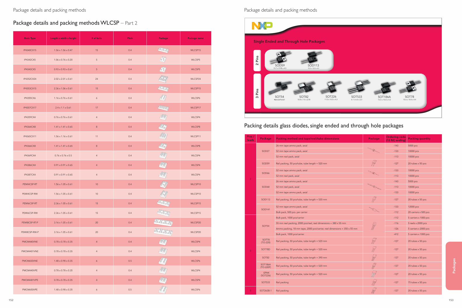
152 153
Pac
kag
es
Package details and packing methods
Package details and packing methods WLCSP – Part 2
Pins /leads Package Packing method and tape/reel/tube dimensions Package
Ordering code (12 NC ending)
Packing quantity
2
SOD27
26 mm tape ammo pack, axial -143 5000 pcs
52 mm tape ammo pack, axial -133 10000 pcs
52 mm reel pack, axial -113 10000 pcs
SOD59 Rail packing, 50 pcs/tube, tube length = 520 mm -127 20 tubes x 50 pcs
SOD6652 mm tape ammo pack, axial -133 10000 pcs
52 mm reel pack, axial -113 10000 pcs
SOD68
26 mm tape ammo pack, axial -143 5000 pcs
52 mm reel pack, axial -113 10000 pcs
52 mm tape ammo pack, axial -133 10000 pcs
SOD113 Rail packing, 50 pcs/tube, tube length = 520 mm -127 20 tubes x 50 pcs
SOD14152 mm tape ammo pack, axial -133 12000 pcs
Bulk pack, 500 pcs. per carrier -112 20 carriers x 500 pcs
3
SOT54
Bulk pack, 1000 pcs/carrier -112 5 carriers x 1000 pcs
55 mm reel packing, 2000 pcs/reel, reel dimensions = 380 x 55 mm -116 5 reels x 2000 pcs
Ammo packing, 18 mm tape, 2000 pcs/carrier, reel dimensions = 350 x 55 mm -126 5 carriers x 2000 pcs
Bulk pack, 1000 pcs/carrier -412 5 carriers x 1000 pcs
SOT78 (TO-220) Rail packing, 50 pcs/tube, tube length = 520 mm -127 20 tubes x 50 pcs
SOT78D Rail packing, 50 pcs/tube, tube length = 520 mm -127 20 tubes x 50 pcs
SOT82 Rail packing, 50 pcs/tube, tube length = 390 mm -127 20 tubes x 50 pcs
SOT186A (TO-220F) Rail packing, 50 pcs/tube, tube length = 520 mm -127 20 tubes x 50 pcs
I2PAK(SOT226) Rail packing, 50 pcs/tube, tube length = 520 mm -127 20 tubes x 50 pcs
SOT533 Rail packing -127 75 tubes x 50 pcs
5 SOT263B-1 Rail packing -127 20 tubes x 50 pcs
M3D
176M3D
130M3D
050
Basic Type Length x width x height # of balls Pitch Package Package name
IP4340CX15 1.56 x 1.56 x 0.47 15 0.4 WLCSP15
IP4342CX5 1.06 x 0.76 x 0.20 5 0.4 WLCSP5
IP4343CX5 0.93 x 0.93 x 0.61 5 0.4 WLCSP5
IP4352CX24 2.02 x 2.01 x 0.61 24 0.4 WLCSP24
IP4353CX15 2.36 x 1.06 x 0.61 15 0.4 WLCSP15
IP4355CX6 1.16 x 0.76 x 0.61 6 0.4 WLCSP6
IP4357CX17 2.4 x 1.1 x 0.61 17 0.4 WLCSP17
IP4359CX4 0.76 x 0.76 x 0.61 4 0.4 WLCSP4
IP4364CX8 1.41 x 1.41 x 0.65 8 0.4 WLCSP8
IP4365CX11 1.56 x 1.16 x 0.61 11 0.4 WLCSP11
IP4366CX8 1.41 x 1.41 x 0.65 8 0.4 WLCSP8
IP4369CX4 0.76 x 0.76 x 0.5 4 0.4 WLCSP4
IP4386CX4 0.91 x 0.91 x 0.65 4 0.4 WLCSP4
IP4387CX4 0.91 x 0.91 x 0.65 4 0.4 WLCSP4
PEMI4CSP-RT 1.56 x 1.05 x 0.61 10 0.4 WLCSP10
PEMI4CSP-RW 1.56 x 1.05 x 0.61 10 0.4 WLCSP10
PEMI6CSP-RT 2.36 x 1.05 x 0.61 15 0.4 WLCSP15
PEMI6CSP-RW 2.36 x 1.05 x 0.61 15 0.4 WLCSP15
PEMI8CSP-RT-P 3.16 x 1.05 x 0.61 20 0.4 WLCSP20
PEMI8CSP-RW-P 3.16 x 1.05 x 0.61 20 0.4 WLCSP20
PMCM440VNE 0.78 x 0.78 x 0.35 4 0.4 WLCSP4
PMCM4401VNE 0.78 x 0.78 x 0.35 4 0.4 WLCSP4
PMCM650VNE 1.48 x 0.98 x 0.35 6 0.5 WLCSP6
PMCM440VPE 0.78 x 0.78 x 0.35 4 0.4 WLCSP4
PMCM4401VPE 0.78 x 0.78 x 0.35 4 0.4 WLCSP4
PMCM650VPE 1.48 x 0.98 x 0.35 6 0.5 WLCSP6
Package details and packing methods
Packing details glass diodes, single ended and through hole packages
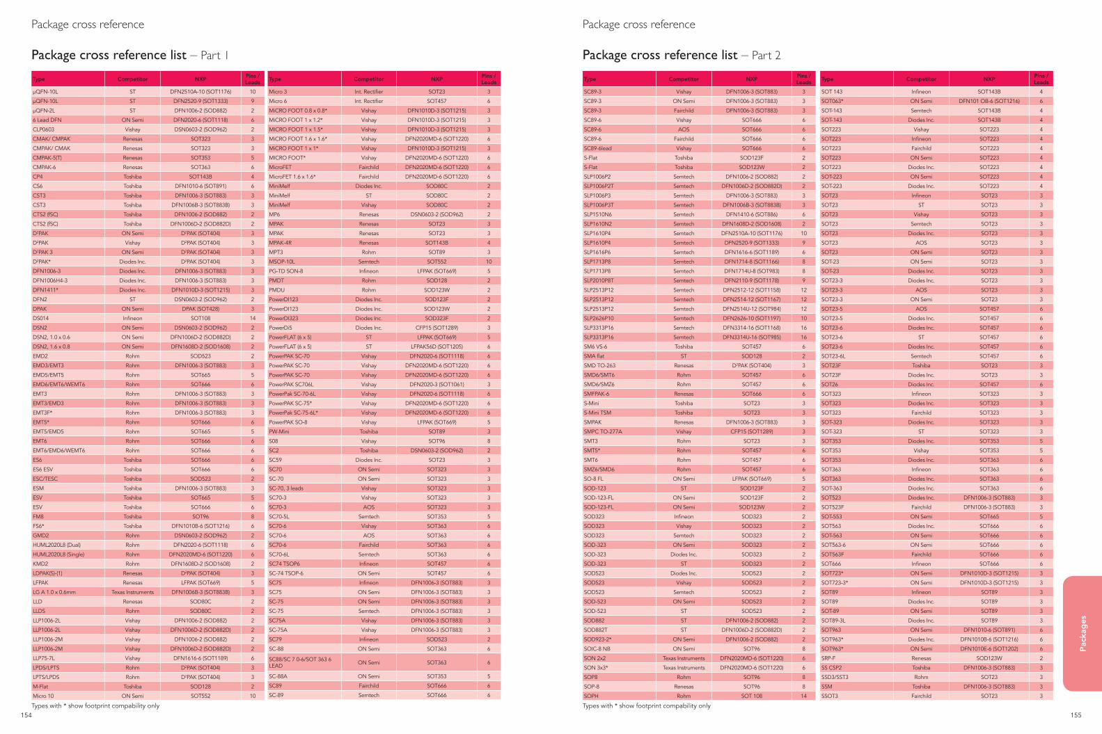
154 155
Pac
kag
es
Package cross reference list – Part 2
Package cross reference
Type Competitor NXP Pins / Leads
SC89-3 Vishay DFN1006-3 (SOT883) 3
SC89-3 ON Semi DFN1006-3 (SOT883) 3
SC89-3 Fairchild DFN1006-3 (SOT883) 3
SC89-6 Vishay SOT666 6
SC89-6 AOS SOT666 6
SC89-6 Fairchild SOT666 6
SC89-6lead Vishay SOT666 6
S-Flat Toshiba SOD123F 2
S-Flat Toshiba SOD123W 2
SLP1006P2 Semtech DFN1006-2 (SOD882) 2
SLP1006P2T Semtech DFN1006D-2 (SOD882D) 2
SLP1006P3 Semtech DFN1006-3 (SOT883) 3
SLP1006P3T Semtech DFN1006B-3 (SOT883B) 3
SLP1510N6 Semtech DFN1410-6 (SOT886) 6
SLP1610N2 Semtech DFN1608D-2 (SOD1608) 2
SLP1610P4 Semtech DFN2510A-10 (SOT1176) 10
SLP1610P4 Semtech DFN2520-9 (SOT1333) 9
SLP1616P6 Semtech DFN1616-6 (SOT1189) 6
SLP1713P8 Semtech DFN1714-8 (SOT1166) 8
SLP1713P8 Semtech DFN1714U-8 (SOT983) 8
SLP2010P8T Semtech DFN2110-9 (SOT1178) 9
SLP2513P12 Semtech DFN2512-12 (SOT1158) 12
SLP2513P12 Semtech DFN2514-12 (SOT1167) 12
SLP2513P12 Semtech DFN2514U-12 (SOT984) 12
SLP2626P10 Semtech DFN2626-10 (SOT1197) 10
SLP3313P16 Semtech DFN3314-16 (SOT1168) 16
SLP3313P16 Semtech DFN3314U-16 (SOT985) 16
SM6 VS-6 Toshiba SOT457 6
SMA flat ST SOD128 2
SMD TO-263 Renesas D2PAK (SOT404) 3
SMD6/SMT6 Rohm SOT457 6
SMD6/SMZ6 Rohm SOT457 6
SMFPAK-6 Renesas SOT666 6
S-Mini Toshiba SOT23 3
S-Mini TSM Toshiba SOT23 3
SMPAK Renesas DFN1006-3 (SOT883) 3
SMPC TO-277A Vishay CFP15 (SOT1289) 3
SMT3 Rohm SOT23 3
SMT5* Rohm SOT457 6
SMT6 Rohm SOT457 6
SMZ6/SMD6 Rohm SOT457 6
SO-8 FL ON Semi LFPAK (SOT669) 5
SOD-123 ST SOD123F 2
SOD-123-FL ON Semi SOD123F 2
SOD-123-FL ON Semi SOD123W 2
SOD323 Infineon SOD323 2
SOD323 Vishay SOD323 2
SOD323 Semtech SOD323 2
SOD-323 ON Semi SOD323 2
SOD-323 Diodes Inc. SOD323 2
SOD-323 ST SOD323 2
SOD523 Diodes Inc. SOD523 2
SOD523 Vishay SOD523 2
SOD523 Semtech SOD523 2
SOD-523 ON Semi SOD523 2
SOD-523 ST SOD523 2
SOD882 ST DFN1006-2 (SOD882) 2
SOD882T ST DFN1006D-2 (SOD882D) 2
SOD923-2* ON Semi DFN1006-2 (SOD882) 2
SOIC-8 NB ON Semi SOT96 8
SON 2x2 Texas Instruments DFN2020MD-6 (SOT1220) 6
SON 3x3* Texas Instruments DFN2020MD-6 (SOT1220) 6
SOP8 Rohm SOT96 8
SOP-8 Renesas SOT96 8
SOPH Rohm SOT 108 14
Type Competitor NXP Pins / Leads
SOT 143 Infineon SOT143B 4
SOT063* ON Semi DFN101 OB-6 (SOT1216) 6
SOT-143 Semtech SOT143B 4
SOT-143 Diodes Inc. SOT143B 4
SOT223 Vishay SOT223 4
SOT223 Infineon SOT223 4
SOT223 Fairchild SOT223 4
SOT223 ON Semi SOT223 4
SOT223 Diodes Inc. SOT223 4
SOT-223 ON Semi SOT223 4
SOT-223 Diodes Inc. SOT223 4
SOT23 Infineon SOT23 3
SOT23 ST SOT23 3
SOT23 Vishay SOT23 3
SOT23 Semtech SOT23 3
SOT23 Diodes Inc. SOT23 3
SOT23 AOS SOT23 3
SOT23 ON Semi SOT23 3
SOT-23 ON Semi SOT23 3
SOT-23 Diodes Inc. SOT23 3
SOT23-3 Diodes Inc. SOT23 3
SOT23-3 AOS SOT23 3
SOT23-3 ON Semi SOT23 3
SOT23-5 AOS SOT457 6
SOT23-5 Diodes Inc. SOT457 6
SOT23-6 Diodes Inc. SOT457 6
SOT23-6 ST SOT457 6
SOT23-6 Diodes Inc. SOT457 6
SOT23-6L Semtech SOT457 6
SOT23F Toshiba SOT23 3
SOT23F Diodes Inc. SOT23 3
SOT26 Diodes Inc. SOT457 6
SOT323 Infineon SOT323 3
SOT323 Diodes Inc. SOT323 3
SOT323 Fairchild SOT323 3
SOT-323 Diodes Inc. SOT323 3
SOT-323 ST SOT323 3
SOT353 Diodes Inc. SOT353 5
SOT353 Vishay SOT353 5
SOT353 Diodes Inc. SOT363 6
SOT363 Infineon SOT363 6
SOT363 Diodes Inc. SOT363 6
SOT-363 Diodes Inc. SOT363 6
SOT523 Diodes Inc. DFN1006-3 (SOT883) 3
SOT523F Fairchild DFN1006-3 (SOT883) 3
SOT-553 ON Semi SOT665 5
SOT563 Diodes Inc. SOT666 6
SOT-563 ON Semi SOT666 6
SOT563-6 ON Semi SOT666 6
SOT563F Fairchild SOT666 6
SOT666 Infineon SOT666 6
SOT723* ON Semi DFN1010D-3 (SOT1215) 3
SOT723-3* ON Semi DFN1010D-3 (SOT1215) 3
SOT89 Infineon SOT89 3
SOT89 Diodes Inc. SOT89 3
SOT-89 ON Semi SOT89 3
SOT89-3L Diodes Inc. SOT89 3
SOT963 ON Semi DFN1010-6 (SOT891) 6
SOT963* Diodes Inc. DFN1010B-6 (SOT1216) 6
SOT963* ON Semi DFN1010E-6 (SOT1202) 6
SRP-F Renesas SOD123W 2
SS CSP2 Toshiba DFN1006-3 (SOT883) 3
SSD3/SST3 Rohm SOT23 3
SSM Toshiba DFN1006-3 (SOT883) 3
SSOT3 Fairchild SOT23 3
Package cross reference list – Part 1
Package cross reference
Type Competitor NXP Pins / Leads
µQFN-10L ST DFN2510A-10 (SOT1176) 10
µQFN-10L ST DFN2520-9 (SOT1333) 9
µQFN-2L ST DFN1006-2 (SOD882) 2
6 Lead DFN ON Semi DFN2020-6 (SOT1118) 6
CLP0603 Vishay DSN0603-2 (SOD962) 2
CMAK/ CMPAK Renesas SOT323 3
CMPAK/ CMAK Renesas SOT323 3
CMPAK-5(T) Renesas SOT353 5
CMPAK-6 Renesas SOT363 6
CP4 Toshiba SOT143B 4
CS6 Toshiba DFN1010-6 (SOT891) 6
CST3 Toshiba DFN1006-3 (SOT883) 3
CST3 Toshiba DFN1006B-3 (SOT883B) 3
CTS2 (fSC) Toshiba DFN1006-2 (SOD882) 2
CTS2 (fSC) Toshiba DFN1006D-2 (SOD882D) 2
D2PAK ON Semi D2PAK (SOT404) 3
D2PAK Vishay D2PAK (SOT404) 3
D2PAK 3 ON Semi D2PAK (SOT404) 3
D2PAK* Diodes Inc. D2PAK (SOT404) 3
DFN1006-3 Diodes Inc. DFN1006-3 (SOT883) 3
DFN1006H4-3 Diodes Inc. DFN1006-3 (SOT883) 3
DFN1411* Diodes Inc. DFN1010D-3 (SOT1215) 3
DFN2 ST DSN0603-2 (SOD962) 2
DPAK ON Semi DPAK (SOT428) 3
DS014 Infineon SOT108 14
DSN2 ON Semi DSN0603-2 (SOD962) 2
DSN2, 1.0 x 0.6 ON Semi DFN1006D-2 (SOD882D) 2
DSN2, 1.6 x 0.8 ON Semi DFN1608D-2 (SOD1608) 2
EMD2 Rohm SOD523 2
EMD3/EMT3 Rohm DFN1006-3 (SOT883) 3
EMD5/EMT5 Rohm SOT665 5
EMD6/EMT6/WEMT6 Rohm SOT666 6
EMT3 Rohm DFN1006-3 (SOT883) 3
EMT3/EMD3 Rohm DFN1006-3 (SOT883) 3
EMT3F* Rohm DFN1006-3 (SOT883) 3
EMT5* Rohm SOT666 6
EMT5/EMD5 Rohm SOT665 5
EMT6 Rohm SOT666 6
EMT6/EMD6/WEMT6 Rohm SOT666 6
ES6 Toshiba SOT666 6
ES6 ESV Toshiba SOT666 6
ESC/TESC Toshiba SOD523 2
ESM Toshiba DFN1006-3 (SOT883) 3
ESV Toshiba SOT665 5
ESV Toshiba SOT666 6
FM8 Toshiba SOT96 8
FS6* Toshiba DFN1010B-6 (SOT1216) 6
GMD2 Rohm DSN0603-2 (SOD962) 2
HUML2020L8 (Dual) Rohm DFN2020-6 (SOT1118) 6
HUML2020L8 (Single) Rohm DFN2020MD-6 (SOT1220) 6
KMD2 Rohm DFN1608D-2 (SOD1608) 2
LDPAK(S)-(1) Renesas D2PAK (SOT404) 3
LFPAK Renesas LFPAK (SOT669) 5
LG A 1.0 x 0.6mm Texas Instruments DFN1006B-3 (SOT883B) 3
LLD Renesas SOD80C 2
LLDS Rohm SOD80C 2
LLP1006-2L Vishay DFN1006-2 (SOD882) 2
LLP1006-2L Vishay DFN1006D-2 (SOD882D) 2
LLP1006-2M Vishay DFN1006-2 (SOD882) 2
LLP1006-2M Vishay DFN1006D-2 (SOD882D) 2
LLP75-7L Vishay DFN1616-6 (SOT1189) 6
LPDS/LPTS Rohm D2PAK (SOT404) 3
LPTS/LPDS Rohm D2PAK (SOT404) 3
M-Flat Toshiba SOD128 2
Micro 10 ON Semi SOT552 10
Type Competitor NXP Pins / Leads
Micro 3 Int. Rectifier SOT23 3
Micro 6 Int. Rectifier SOT457 6
MiCRO FOOT 0.8 x 0.8* Vishay DFN1010D-3 (SOT1215) 3
MiCRO FOOT 1 x 1.2* Vishay DFN1010D-3 (SOT1215) 3
MICRO FOOT 1 x 1.5* Vishay DFN1010D-3 (SOT1215) 3
MiCRO FOOT 1.6 x 1.6* Vishay DFN2020MD-6 (SOT1220) 6
MiCRO FOOT 1 x 1* Vishay DFN1010D-3 (SOT1215) 3
MICRO FOOT* Vishay DFN2020MD-6 (SOT1220) 6
MicroFET Fairchild DFN2020MD-6 (SOT1220) 6
MicroFET 1.6 x 1.6* Fairchild DFN2020MD-6 (SOT1220) 6
MiniMelf Diodes Inc. SOD80C 2
MiniMelf ST SOD80C 2
MiniMelf Vishay SOD80C 2
MP6 Renesas DSN0603-2 (SOD962) 2
MPAK Renesas SOT23 3
MPAK Renesas SOT23 3
MPAK-4R Renesas SOT143B 4
MPT3 Rohm SOT89 3
MSOP-10L Semtech SOT552 10
PG-TD SON-8 Infineon LFPAK (SOT669) 5
PMDT Rohm SOD128 2
PMDU Rohm SOD123W 2
PowerDI123 Diodes Inc. SOD123F 2
PowerDI123 Diodes Inc. SOD123W 2
PowerDI323 Diodes Inc. SOD323F 2
PowerDi5 Diodes Inc. CFP15 (SOT1289) 3
PowerFLAT (6 x 5) ST LFPAK (SOT669) 5
PowerFLAT (6 x 5) ST LFPAK56D (SOT1205) 6
PowerPAK SC-70 Vishay DFN2020-6 (SOT1118) 6
PowerPAK SC-70 Vishay DFN2020MD-6 (SOT1220) 6
PowerPAK SC-70 Vishay DFN2020MD-6 (SOT1220) 6
PowerPAK SC706L Vishay DFN2020-3 (SOT1061) 3
PowerPak SC-70-6L Vishay DFN2020-6 (SOT1118) 6
PowerPAK SC-75* Vishay DFN2020MD-6 (SOT1220) 6
PowerPak SC-75-6L* Vishay DFN2020MD-6 (SOT1220) 6
PowerPAK SO-8 Vishay LFPAK (SOT669) 5
PW-Mini Toshiba SOT89 3
S08 Vishay SOT96 8
SC2 Toshiba DSN0603-2 (SOD962) 2
SC59 Diodes Inc. SOT23 3
SC70 ON Semi SOT323 3
SC-70 ON Semi SOT323 3
SC-70, 3 leads Vishay SOT323 3
SC70-3 Vishay SOT323 3
SC70-3 AOS SOT323 3
SC70-5L Semtech SOT353 5
SC70-6 Vishay SOT363 6
SC70-6 AOS SOT363 6
SC70-6 Fairchild SOT363 6
SC70-6L Semtech SOT363 6
SC74 TSOP6 Infineon SOT457 6
SC-74 TSOP-6 ON Semi SOT457 6
SC75 Infineon DFN1006-3 (SOT883) 3
SC75 ON Semi DFN1006-3 (SOT883) 3
SC-75 ON Semi DFN1006-3 (SOT883) 3
SC-75 Semtech DFN1006-3 (SOT883) 3
SC75A Vishay DFN1006-3 (SOT883) 3
SC-75A Vishay DFN1006-3 (SOT883) 3
SC79 Infineon SOD523 2
SC-88 ON Semi SOT363 6
SC88/SC 7 0-6/SOT 363 6 LEAD ON Semi SOT363 6
SC-88A ON Semi SOT353 5
SC89 Fairchild SOT666 6
SC-89 Semtech SOT666 6
Types with * show footprint compability only Types with * show footprint compability only
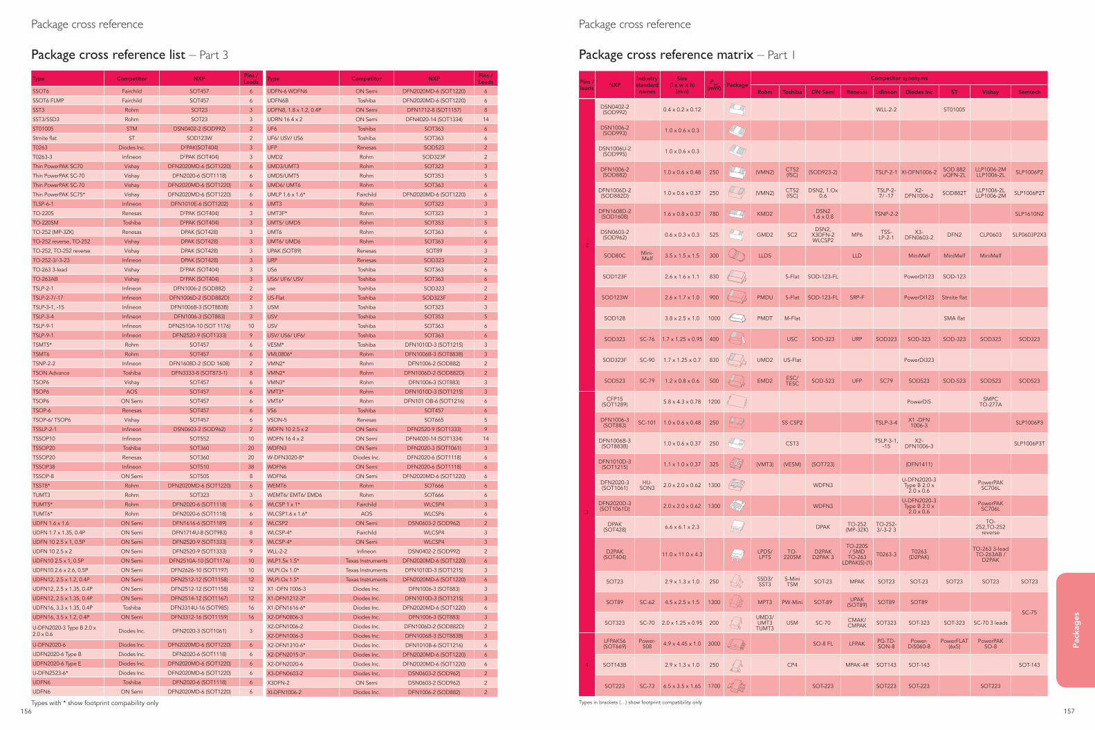
156 157
Pac
kag
es
Package cross reference
Types with * show footprint compability only
Package cross reference list – Part 3
Type Competitor NXP Pins / Leads
SSOT6 Fairchild SOT457 6
SSOT6 FLMP Fairchild SOT457 6
SST3 Rohm SOT23 3
SST3/SSD3 Rohm SOT23 3
ST01005 STM DSN0402-2 (SOD992) 2
Stmite flat ST SOD123W 2
T0263 Diodes Inc. D2PAK(SOT404) 3
T0263-3 Infineon D2PAK (SOT404) 3
Thin PowerPAK SC70 Vishay DFN2020MD-6 (SOT1220) 6
Thin PowerPAK SC-70 Vishay DFN2020-6 (SOT1118) 6
Thin PowerPAK SC-70 Vishay DFN2020MD-6 (SOT1220) 6
Thin PowerPAK SC75* Vishay DFN2020MD-6 (SOT1220) 6
TLSP-6-1 Infineon DFN1010E-6 (SOT1202) 6
TO-220S Renesas D2PAK (SOT404) 3
TO-220SM Toshiba D2PAK (SOT404) 3
TO-252 (MP-3ZK) Renesas DPAK (SOT428) 3
TO-252 reverse, TO-252 Vishay DPAK (SOT428) 3
TO-252, TO-252 reverse Vishay DPAK (SOT428) 3
TO-252-3/-3-23 Infineon DPAK (SOT428) 3
TO-263 3-lead Vishay D2PAK (SOT404) 3
TO-263AB Vishay D2PAK (SOT404) 3
TSLP-2-1 Infineon DFN1006-2 (SOD882) 2
TSLP-2-7/-17 Infineon DFN1006D-2 (SOD882D) 2
TSLP-3-1, -15 Infineon DFN1006B-3 (SOT883B) 3
TSLP-3-4 Infineon DFN1006-3 (SOT883) 3
TSLP-9-1 Infineon DFN2510A-10 (SOT 1176) 10
TSLP-9-1 Infineon DFN2520-9 (SOT1333) 9
TSMT5* Rohm SOT457 6
TSMT6 Rohm SOT457 6
TSNP-2-2 Infineon DFN1608D-2 (SOD 1608) 2
TSON Advance Toshiba DFN3333-8 (SOT873-1) 8
TSOP6 Vishay SOT457 6
TSOP6 AOS SOT457 6
TSOP6 ON Semi SOT457 6
TSOP-6 Renesas SOT457 6
TSOP-6/ TSOP6 Vishay SOT457 6
TSSLP-2-1 Infineon DSN0603-2 (SOD962) 2
TSSOP10 Infineon SOT552 10
TSSOP20 Toshiba SOT360 20
TSSOP20 Renesas SOT360 20
TSSOP38 Infineon SOT510 38
TSSOP-8 ON Semi SOT505 8
TSST8* Rohm DFN2020MD-6 (SOT1220) 6
TUMT3 Rohm SOT323 3
TUMT5* Rohm DFN2020-6 (SOT1118) 6
TUMT6* Rohm DFN2020-6 (SOT1118) 6
UDFN 1.6 x 1.6 ON Semi DFN1616-6 (SOT1189) 6
UDFN 1.7 x 1.35, 0.4P ON Semi DFN1714U-8 (SOT983) 8
UDFN 10 2.5 x 1, 0.5P ON Semi DFN2520-9 (SOT1333) 9
UDFN 10 2.5 x 2 ON Semi DFN2520-9 (SOT1333) 9
UDFN10 2.5 x 1, 0.5P ON Semi DFN2510A-10 (SOT1176) 10
UDFN10 2.6 x 2.6, 0.5P ON Semi DFN2626-10 (SOT1197) 10
UDFN12, 2.5 x 1.2, 0.4P ON Semi DFN2512-12 (SOT1158) 12
UDFN12, 2.5 x 1.35, 0.4P ON Semi DFN2512-12 (SOT1158) 12
UDFN12, 2.5 x 1.35, 0.4P ON Semi DFN2514-12 (SOT1167) 12
UDFN16, 3.3 x 1.35, 0.4P Toshiba DFN3314U-16 (SOT985) 16
UDFN16, 3.5 x 1.2, 0.4P ON Semi DFN3312-16 (SOT1159) 16
U-DFN2020-3 Type B 2.0 x 2.0 x 0.6 Diodes Inc. DFN2020-3 (SOT1061) 3
U-DFN2020-6 Diodes Inc. DFN2020MD-6 (SOT1220) 6
UDFN2020-6 Type B Diodes Inc. DFN2020-6 (SOT1118) 6
UDFN2020-6 Type E Diodes Inc. DFN2020MD-6 (SOT1220) 6
U-DFN2523-6* Diodes Inc. DFN2020MD-6 (SOT1220) 6
UDFN6 Toshiba DFN2020-6 (SOT1118) 6
UDFN6 ON Semi DFN2020MD-6 (SOT1220) 6
Type Competitor NXP Pins / Leads
UDFN-6 WDFN6 ON Semi DFN2020MD-6 (SOT1220) 6
UDFN6B Toshiba DFN2020MD-6 (SOT1220) 6
UDFN8, 1.8 x 1.2, 0.4P ON Semi DFN1712-8 (SOT1157) 8
UDRN 16 4 x 2 ON Semi DFN4020-14 (SOT1334) 14
UF6 Toshiba SOT363 6
UF6/ USV/ US6 Toshiba SOT363 6
UFP Renesas SOD523 2
UMD2 Rohm SOD323F 2
UMD3/UMT3 Rohm SOT323 3
UMD5/UMT5 Rohm SOT353 5
UMD6/ UMT6 Rohm SOT363 6
UMLP 1.6 x 1.6* Fairchild DFN2020MD-6 (SOT1220) 6
UMT3 Rohm SOT323 3
UMT3F* Rohm SOT323 3
UMT5/ UMD5 Rohm SOT353 5
UMT6 Rohm SOT363 6
UMT6/ UMD6 Rohm SOT363 6
UPAK (SOT89) Renesas SOT89 3
URP Renesas SOD323 2
US6 Toshiba SOT363 6
US6/ UF6/ USV Toshiba SOT363 6
use Toshiba SOD323 2
US-Flat Toshiba SOD323F 2
USM Toshiba SOT323 3
USV Toshiba SOT353 5
USV Toshiba SOT363 6
USV/ US6/ UF6/ Toshiba SOT363 6
VESM* Toshiba DFN1010D-3 (SOT1215) 3
VML0806* Rohm DFN1006B-3 (SOT883B) 3
VMN2* Rohm DFN1006-2 (SOD882) 2
VMN2* Rohm DFN1006D-2 (SOD882D) 2
VMN3* Rohm DFN1006-3 (SOT883) 3
VMT3* Rohm DFN1010D-3 (SOT1215) 3
VMT6* Rohm DFN101 OB-6 (SOT1216) 6
VS6 Toshiba SOT457 6
VSON-5 Renesas SOT665 5
WDFN 10 2.5 x 2 ON Semi DFN2520-9 (SOT1333) 9
WDFN 16 4 x 2 ON Semi DFN4020-14 (SOT1334) 14
WDFN3 ON Semi DFN2020-3 (SOT1061) 3
W-DFN3020-8* Diodes Inc. DFN2020-6 (SOT1118) 6
WDFN6 ON Semi DFN2020-6 (SOT1118) 6
WDFN6 ON Semi DFN2020MD-6 (SOT1220) 6
WEMT6 Rohm SOT666 6
WEMT6/ EMT6/ EMD6 Rohm SOT666 6
WLCSP 1 x 1* Fairchild WLCSP4 3
WLCSP1.6 x 1.6* AOS WLCSP6 6
WLCSP2 ON Semi DSN0603-2 (SOD962) 2
WLCSP-4* Fairchild WLCSP4 3
WLCSP-4* ON Semi WLCSP4 3
WLL-2-2 Infineon DSN0402-2 (SOD992) 2
WLP1.5x 1.5* Texas Instruments DFN2020MD-6 (SOT1220) 6
WLPI.Ox 1.0* Texas Instruments DFN1010D-3 (SOT1215) 3
WLPI.Ox 1.5* Texas Instruments DFN2020MD-6 (SOT1220) 6
X1 -DFN 1006-3 Diodes Inc. DFN1006-3 (SOT883) 3
X1-DFN1212-3* Diodes Inc. DFN1010D-3 (SOT1215) 3
X1-DFN1616-6* Diodes Inc. DFN2020MD-6 (SOT1220) 6
X2-DFN0806-3 Diodes Inc. DFN1006-3 (SOT883) 3
X2-DFN1006-2 Diodes Inc. DFN1006D-2 (SOD882D) 2
X2-DFN1006-3 Diodes Inc. DFN1006B-3 (SOT883B) 3
X2-DFN1310-6* Diodes Inc. DFN1010B-6 (SOT1216) 6
X2-DFN2015-3* Diodes Inc. DFN2020MD-6 (SOT1220) 6
X2-DFN2020-6 Diodes Inc. DFN2020MD-6 (SOT1220) 6
X3-DFN0603-2 Diodes Inc. DSN0603-2 (SOD962) 2
X3DFN-2 ON Semi DSN0603-2 (SOD962) 2
XI-DFN1006-2 Diodes Inc. DFN1006-2 (SOD882) 2
Package cross reference
Pins / leads NXP
Industry standard names
Size(l x w x h)
(mm)
Ptot(mW) Package
Competitor synonyms
Rohm Toshiba ON Semi Renesas Infineon Diodes Inc ST Vishay Semtech
2
DSN0402-2 (SOD992) 0.4 x 0.2 x 0.12 WLL-2-2 ST01005
DSN1006-2 (SOD993) 1.0 x 0.6 x 0.3
DSN1006U-2 (SOD995) 1.0 x 0.6 x 0.3
DFN1006-2 (SOD882) 1.0 x 0.6 x 0.48 250 (VMN2) CTS2
(fSC) (SOD923-2) TSLP-2-1 XI-DFN1006-2 SOD 882 uQFN-2L
LLP1006-2M LLP1006-2L SLP1006P2
DFN1006D-2 (SOD882D) 1.0 x 0.6 x 0.37 250 (VMN2) CTS2
(fSC)DSN2, 1.Ox
0.6TSLP-2-7/ -17
X2-DFN1006-2 SOD882T LLP1006-2L
LLP1006-2M SLP1006P2T
DFN1608D-2 (SOD1608) 1.6 x 0.8 x 0.37 780 KMD2 DSN2
1.6 x 0.8 TSNP-2-2 SLP1610N2
DSN0603-2 (SOD962) 0.6 x 0.3 x 0.3 525 GMD2 SC2
DSN2, X3DFN-2 WLCSP2
MP6 TSS-LP-2-1
X3-DFN0603-2 DFN2 CLP0603 SLP0603P2X3
SOD80C Mini- Melf 3.5 x 1.5 x 1.5 300 LLDS LLD MiniMelf MiniMelf MiniMelf
SOD123F 2.6 x 1.6 x 1.1 830 S-Flat SOD-123-FL PowerDI123 SOD-123
SOD123W 2.6 x 1.7 x 1.0 900 PMDU S-Flat SOD-123-FL SRP-F PowerDI123 Stmite flat
SOD128 3.8 x 2.5 x 1.0 1000 PMDT M-Flat SMA flat
SOD323 SC-76 1.7 x 1.25 x 0.95 400 USC SOD-323 URP SOD323 SOD-323 SOD-323 SOD323 SOD323
SOD323F SC-90 1.7 x 1.25 x 0.7 830 UMD2 US-Flat PowerDI323
SOD523 SC-79 1.2 x 0.8 x 0.6 500 EMD2 ESC/TESC SOD-523 UFP SC79 SOD523 SOD-523 SOD523 SOD523
3
CFP15 (SOT1289) 5.8 x 4.3 x 0.78 1200 PowerDi5 SMPC
TO-277A
DFN1006-3 (SOT883) SC-101 1.0 x 0.6 x 0.48 250 SS CSP2 TSLP-3-4 X1 -DFN
1006-3 SLP1006P3
DFN1006B-3 (SOT883B) 1.0 x 0.6 x 0.37 250 CST3 TSLP-3-1,
-15X2-
DFN1006-3 SLP1006P3T
DFN1010D-3 (SOT1215) 1.1 x 1.0 x 0.37 325 (VMT3) (VESM) (SOT723) (DFN1411)
DFN2020-3 (SOT1061)
HU- SON3 2.0 x 2.0 x 0.62 1300 WDFN3
U-DFN2020-3 Type B 2.0 x
2.0 x 0.6PowerPAK
SC706L
DFN2020D-3 (SOT1061D) 2.0 x 2.0 x 0.62 1300 WDFN3
U-DFN2020-3 Type B 2.0 x
2.0 x 0.6PowerPAK
SC706L
DPAK (SOT428) 6.6 x 6.1 x 2.3 DPAK TO-252
(MP-3ZK)TO-252-3/-3-2 3
TO-252,TO-252
reverse
D2PAK (SOT404) 11.0 x 11.0 x 4.3 LPDS/
LPTSTO-
220SMD2PAK
D2PAK 3
TO-220S / SMD
TO-263 LDPAK(S)-(1)
T0263-3 T0263 (D2PAK)
TO-263 3-lead TO-263AB /
D2PAK
SOT23 2.9 x 1.3 x 1.0 250 SSD3/ SST3
S-Mini TSM SOT-23 MPAK SOT23 SOT-23 SOT23 SOT23 SOT23
SOT89 SC-62 4.5 x 2.5 x 1.5 1300 MPT3 PW-Mini SOT-89 UPAK (SOT89) SOT89 SOT89
SC-75
SOT323 SC-70 2.0 x 1.25 x 0.95 200UMD3/ UMT3
TUMT3USM SC-70 CMAK/
CMPAK SOT323 SOT-323 SOT-323 SC-70 3 leads
4
LFPAK56 (SOT669)
Power- S08 4.9 x 4.45 x 1.0 3000 SO-8 FL LFPAK PG-TD-
SON-8Power-
Di5060-8PowerFLAT
(6x5)PowerPAK
SO-8
SOT143B 2.9 x 1.3 x 1.0 250 CP4 MPAK-4R SOT143 SOT-143 SOT-143
SOT223 SC-73 6.5 x 3.5 x 1.65 1700 SOT-223 SOT223 SOT-223 SOT223
Package cross reference matrix – Part 1
M3D088
M3D109
Types in brackets (…) show footprint compatibility only
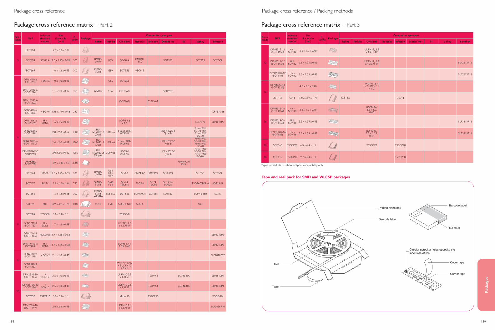
158 159
Pac
kag
es
Package cross reference
Package cross reference matrix – Part 2
Package cross reference / Packing methods
Tape and reel pack for SMD and WLCSP packages
Cover tape
Circular sprocket holes opposite thelabel side of reel
Carrier tape
msc074
QA Seal
Tape
Reel
Barcode label
Barcode label
Printed plano box
Printed plano boxTapeLabelsReelCover tapeCarrier tapeSeal
Item Material Weight (1) (g)
(1) For SOD87 (180 x 8)
Cardboard carbon coatedPaperPaperPolystyrenePolyestherPolystyreneAcrylate
48.000.180.91
42.503.00
15.400.15
Pins / leads NXP
Industry standard names
Size(l x w x h)
(mm)
Ptot(mW) Package
Competitor synonyms
Rohm Toshiba ON Semi Renesas Infineon Diodes Inc ST Vishay Semtech
5
SOT753 2.9 x 1.5 x 1.0
SOT353 SC-88 A 2.0 x 1.25 x 0.95 300 UMD5/ UMT5 USV SC-88 A CMPAK-
5C0 SOT353 SOT353 SC70-5L
SOT665 1.6 x 1.2 x 0.55 300 EMD5/ EMT5 ESV SOT-553 VSON-5
6
DFN1010-6 (SOT891) x SON6 1.0 x 1.0 x 0.48 CS6 SOT963
DFN1010B-6 (SOT1216) 1.1 x 1.0 x 0.37 350 (VMT6) (FS6) (SOT063) (SOT963)
DFN1010E-6 (SOT1202) (SOT963) TLSP-6-1
DFN1410-6 (SOT886) x SON6 1.45 x 1.0 x 0.48 250 SLP1510N6
DFN1616-6 (SOT1189)
H x SON6 1.6 x 1.6 x 0.48 UDFN 1.6
x 1.6 LLP75-/L SLP1616P6
DFN2020-6 (SOT1118) 2.0 x 2.0 x 0.62 1300
HU- ML2020L8
(Dual)UDFN6 6 Lead DFN
WDFN6UDFN2020-6
Type B
PowerPAK SC-70 Thin PowerPAK
SC-70
DFN2020D-6 (SOT1118D) 2.0 x 2.0 x 0.62 1300
HU- ML2020L8
(Dual)UDFN6 6 Lead DFN
WDFN6UDFN2020-6
Type B
PowerPAK SC-70 Thin PowerPAK
SC-70
DFN2020MD-6 (SOT1220) 2.0 x 2.0 x 0.62 1250
HU- ML2020L8
(Single)UDFN6B UDFN-6
WDFN6UDFN2020-6
Type E
PowerPAK SC-70 Thin PowerPAK
SC-70
LFPAK56D (SOT1205) 4.9 x 4.45 x 1.0 3000 PowerFLAT
(6x5)
SOT363 SC-88 2.0 x 1.25 x 0.95 300 UMD6/ UMT6
US6 UF6 USV
SC-88 CMPAK-6 SOT363 SOT-363 SC70-6 SC70-6L
SOT457 SC-74 2.9 x 1.5 x 1.0 750 SMD6/ SMT6
SM6 VS-6
SC-74 TSOP-6 TSOP-6 SC74
TSOP6SOT23-6 SOT26 TSOP6 TSOP-6 SOT23-6L
SOT666 1.6 x 1.2 x 0.55 300EMD6/ EMT6
WEMT6ES6 ESV SOT-563 SMFPAK-6 SOT666 SOT563 SC89-6lead SC-89
8
SOT96 S08 4.9 x 3.9 x 1.75 1500 SOP8 FM8 SOIC-8 NB SOP-8 S08
SOT505 TSSOP8 3.0 x 3.0 x 1.1 TSSOP-8
DFN1712-8 (SOT1157)
H x SON8 1.7 x 1.2 x 0.48 UDFN8, 1.8
x 1.2, 0.4P
DFN1714-8 (SOT 1166) HUSON8 1.7 x 1.35 x 0.52 SLP1713P8
DFN1714U-8 (SOT983)
H x SON8 1.7 x 1.35 x 0.48 UDFN 1.7 x
1.35, 0.4P SLP1713P8
9
DFN2110-9 (SOT1178) x SON9 2.1 x 1.0 x 0.48 SLP2010P8T
DFN2520-9 (SOT1333)
WDFN 10 2.5 x 2 UDFN10
2.5 x 2
10
DFN2510-10 (SOT 1165)
x SON10 2.5 x 1.0 x 0.48 UDFN10 2.5
x 1, 0.5P TSLP-9-1 pQFN-10L SLP1610P4
DFN2510A-10 (SOT1176)
x SON10 2.5 x 1.0 x 0.48 UDFN10 2.5
x 1, 0.5P TSLP-9-1 pQFN-10L SLP1610P4
SOT552 TSSOP10 3.0 x 3.0 x 1.1 Micro 10 TSSOP10 MSOP-10L
DFN2626-10 (SOT 1197) 2.6 x 2.6 x 0.48 UDFN10 2.6
x 2.6, 0.5P SLP2626P10
Pins / leads NXP
Industry standard names
Size(l x w x h)
(mm)
Ptot(mW) Package
Competitor synonyms
Rohm Toshiba ON Semi Renesas Infineon Diodes Inc ST Vishay Semtech
12
DFN2512-12 (SOT 1158)
H x - SON12 2.5 x 1.2 x 0.48 UDFN12, 2.5
x 1.2, 0.4P
DFN2514-12 (SOT 1167)
HU- SON12 2.5 x 1.35 x 0.53 UDFN12, 2.5
x 1.35, 0.4P SLP2513P12
DFN2514U-12 (SOT984)
H x - SON12 2.5 x 1.35 x 0.48 SLP2513P12
14
DFN4020-14 (SOT 1334) 4.0 x 2.0 x 0.48
WDFN 16 4 x 2 UDRN 16
4 x 2
SOT 108 S014 8.65 x 3.9 x 1.75 SOP 14 DS014
16
DFN3312-16 (SOT 1159)
H x - SON16 3.3 x 1.2 x 0.48
UDFN 16, 3.5 x 1.2,
0.4P
DFN3314-16 (SOT 1168)
HU- SON16 3.3 x 1.35 x 0.53 SLP3313P16
DFN3314U-16 (SOT985)
H x - SON16 3.3 x 1.35 x 0.48
UDFN 16, 3.3 x 1.35,
0.4PSLP3313P16
20 SOT360 TSSOP20 6.5 x 4.4 x 1.1 TSSOP20 TSSOP20
38 SOT510 TSSOP38 9.7 x 4.4 x 1.1 TSSOP38
Package cross reference matrix – Part 3
Types in brackets (…) show footprint compatibility only
M3D505
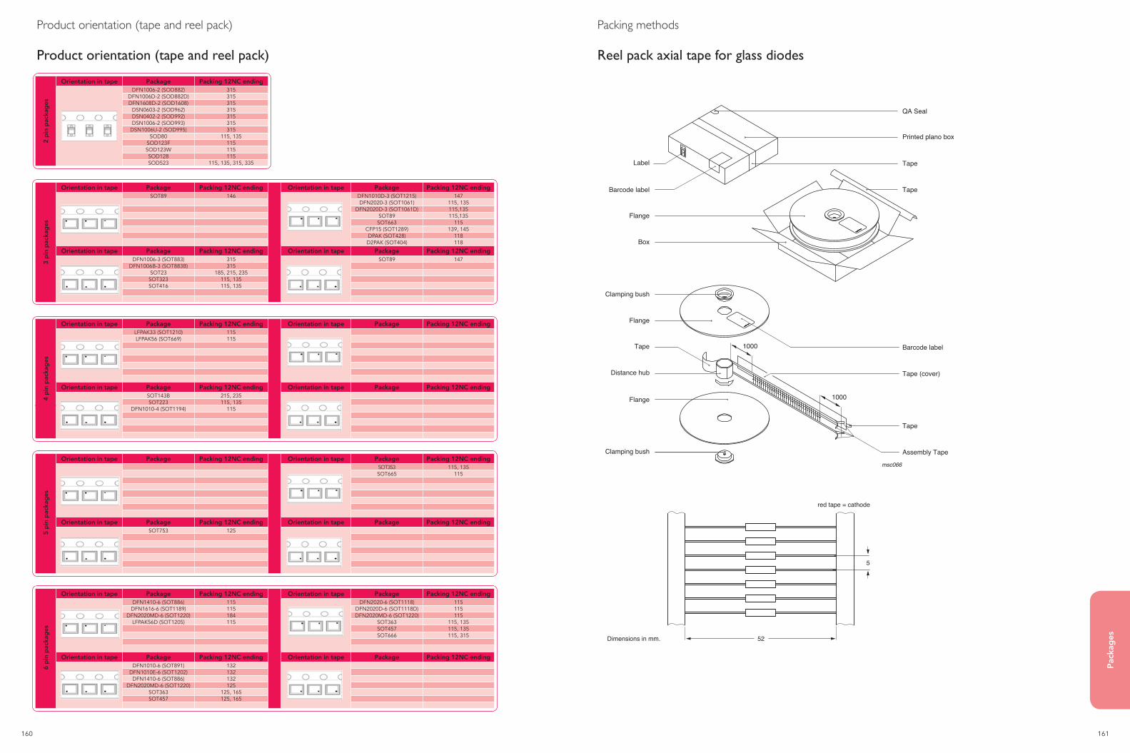
160 161
Pac
kag
es
Product orientation (tape and reel pack)
Product orientation (tape and reel pack)
2 p
in p
acka
ges
Orientation in tape Package Packing 12NC endingDFN1006-2 (SOD882) 315
DFN1006D-2 (SOD882D) 315DFN1608D-2 (SOD1608) 315
DSN0603-2 (SOD962) 315DSN0402-2 (SOD992) 315DSN1006-2 (SOD993) 315
DSN1006U-2 (SOD995) 315SOD80 115, 135
SOD123F 115SOD123W 115SOD128 115SOD523 115, 135, 315, 335
3 p
in p
acka
ges
Orientation in tape Package Packing 12NC ending Orientation in tape Package Packing 12NC endingSOT89 146 DFN1010D-3 (SOT1215) 147
DFN2020-3 (SOT1061) 115, 135DFN2020D-3 (SOT1061D) 115,135
SOT89 115,135SOT663 115
CFP15 (SOT1289) 139, 145DPAK (SOT428) 118
D2PAK (SOT404) 118
Orientation in tape Package Packing 12NC ending Orientation in tape Package Packing 12NC endingDFN1006-3 (SOT883) 315 SOT89 147
DFN1006B-3 (SOT883B) 315SOT23 185, 215, 235SOT323 115, 135SOT416 115, 135
4 p
in p
acka
ges
Orientation in tape Package Packing 12NC ending Orientation in tape Package Packing 12NC endingLFPAK33 (SOT1210) 115LFPAK56 (SOT669) 115
Orientation in tape Package Packing 12NC ending Orientation in tape Package Packing 12NC endingSOT143B 215, 235SOT223 115, 135
DFN1010-4 (SOT1194) 115
5 p
in p
acka
ges
Orientation in tape Package Packing 12NC ending Orientation in tape Package Packing 12NC endingSOT353 115, 135SOT665 115
Orientation in tape Package Packing 12NC ending Orientation in tape Package Packing 12NC endingSOT753 125
6 p
in p
acka
ges
Orientation in tape Package Packing 12NC ending Orientation in tape Package Packing 12NC endingDFN1410-6 (SOT886) 115 DFN2020-6 (SOT1118) 115
DFN1616-6 (SOT1189) 115 DFN2020D-6 (SOT1118D) 115DFN2020MD-6 (SOT1220) 184 DFN2020MD-6 (SOT1220) 115
LFPAK56D (SOT1205) 115 SOT363 115, 135SOT457 115, 135SOT666 115, 315
Orientation in tape Package Packing 12NC ending Orientation in tape Package Packing 12NC endingDFN1010-6 (SOT891) 132
DFN1010E-6 (SOT1202) 132DFN1410-6 (SOT886) 132
DFN2020MD-6 (SOT1220) 125SOT363 125, 165SOT457 125, 165
Reel pack axial tape for glass diodes
msc081
52Dimensions in mm.
5
red tape = cathode
Packing methods
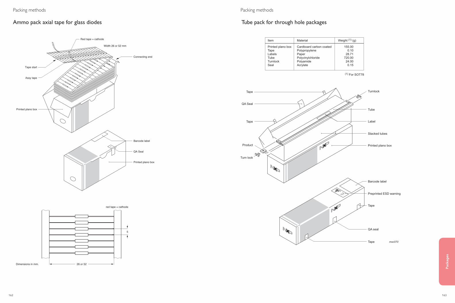
162 163
Pac
kag
es
Turn lock
Product
Tape
QA Seal
Tape
QA seal
Tape
Preprinted ESD warning
Barcode label
Printed plano box
Stacked tubes
Label
Tube
Turnlock
Tape msc070
Printed plano boxTapeLabelsTubeTurnlockSeal
Item Material Weight (1) (g)
(1) For SOT78
Cardboard carbon coatedPolypropylenePaperPolyvinylchloridePolyamideAcrylate
155.000.10
28.71720.0024.000.15
Tube pack for through hole packages
Packing methods
Ammo pack axial tape for glass diodes
Printed plano box
QA Seal
Barcode label
Assy tape
Printed plano box
Tape start
Red tape = cathode
Width 26 or 52 mm
Connecting end
msc073
Printed plano boxAssy tapeLabelsTapeQA Seal
Item Material Weight (1) (g)
(1) For SOD84 52mm
Cardboard carbon coatedPaperPaperPolypropyleneAcrylate
40.0032.49
0.710.250.15
msc081
26 or 52Dimensions in mm.
5
red tape = cathode
Packing methods
164 165
Pac
kag
es
8-pin SMD packages 177DFN1712-8 (SOT1157) 177DFN1714-8 (SOT1166) 177DFN1714U-8 (SOT983) 178DFN3333-8 (SOT873-1) 178SOT96 (SO8) 178SOT505 (TSSOP8) 178
More than 8-pin SMD packages 179DFN2110-9 (SOT1178) 179DFN2510-10 (SOT1165) 179DFN2510A-10 (SOT1176) 179DFN2512-12 (SOT1158) 179DFN2514-12 (SOT1167) 180DFN2514U-12 (SOT984) 180DFN2520-9 (SOT1333) 180DFN2521-12 (SOT1156) 180DFN2626-10 (SOT1197) 181DFN3312-16 (SOT1159) 181DFN3314-16 (SOT1168) 181DFN3314U-16 (SOT985) 181DFN4020-14 (SOT1334) 182DFN5050-32 (SOT617) 182SOT108 (SO14) 182SOT163 (SO20) 182SOT337 (SSOP14) 183SOT357 183SOT360 (TSSOP20) 183SOT402 (TSSOP14) 183SOT510 (TSSOP38) 184SOT519 (SSOP16) 184SOT552 (TSSOP10) 184
Glass diodes 185SOD141 (DO201AD) 185SOD27 (DO-35) 185SOD66 (DO-41) 185SOD68 (DO-34) 185
Single-ended and through-hole packages 185SOT54 (TO92) 185SOD59 185SOT78 (TO220AB) 186SOT78D 186SOT82 186SOD113 186SOT186A (isolated TO220AB) 187SOT226 187SOT263B-1 187SOT533 187
Outline and footprint drawings
Minimized outline drawings and reflow soldering footprint
2-pin SMD packages 166DSN0402-2 (SOD992) 166DSN1006-2 (SOD993) 166DSN1006U-2 (SOD995) 166DFN1006-2 (SOD882) 166DFN1006D-2 (SOD882D) 167DFN1608D-2 (SOD1608) 167DSN0603-2 (SOD962) 167SOD80C 167SOD123F 168SOD123W 168SOD128 168SOD323 (SC-76) 168SOD323F (SC-90) 169SOD523 (SC-79) 169
3-pin SMD packages 169CFP15 (SOT1289) 169DFN1006-3 (SOT883) 169DFN1006B-3 (SOT883B) 170DFN1010D-3 (SOT1215) 170DFN2020-3 (SOT1061) 170DFN2020D-3 (SOT1061D) 170DPAK (SOT428) 171D2PAK (SOT404) 171SOT23 171SOT89 (SC-62) 171SOT323 (SC-70) 172SOT663 172
4-pin SMD packages 172LFPAK33 (SOT1210) 172LFPAK56 (SOT669) 172SOT143B 173SOT223 (SC-73) 173
5-pin SMD packages 173SOT353 (SC-88A) 173SOT665 173
6-pin SMD packages 174DFN1010-6 (SOT891) 174DFN1010B-6 (SOT1216) 174DFN1010E-6 (SOT1202) 174DFN1410-6 (SOT886) 174DFN1616-6 (SOT1189) 175DFN2020-6 (SOT1118) 175DFN2020D-6 (SOT1118D) 175DFN2020MD-6 (SOT1220) 175LFPAK56D (SOT1205) 176SOT363 (SC-88) 176SOT457 (SC-74) 176SOT666 176
7-pin SMD Packages 177DFN2111-7 (SOT1358) 177D2PAK-7 (SOT428) 177
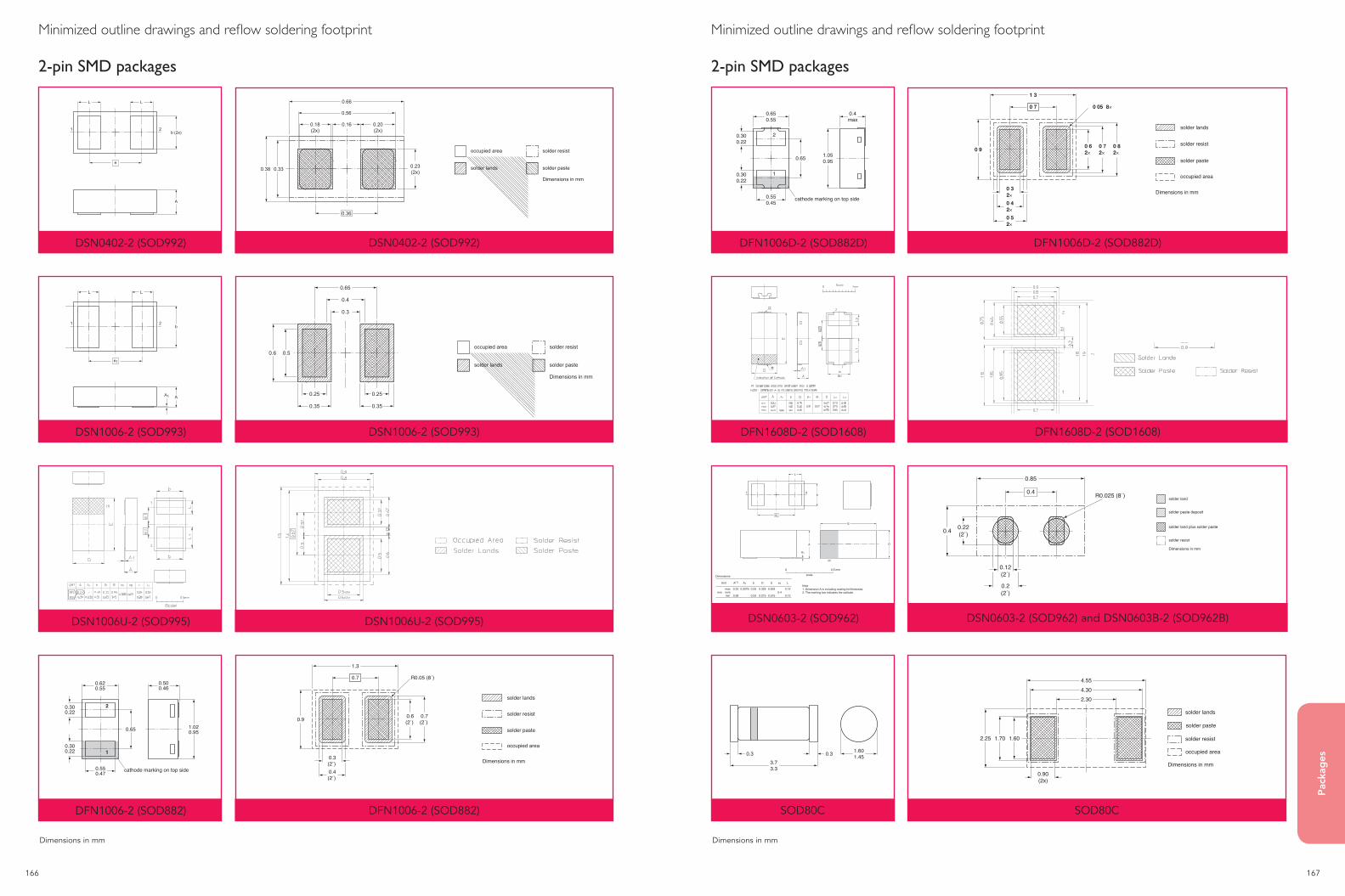
166 167
Pac
kag
es
ReferencesOutlineversion
Europeanprojection Issue date
IEC JEDEC JEITA
SOD992
sod992_po
13-10-2813-11-01
Unit
mmmaxnommin
0.14 0.42 0.12 0.170.250.40
0.38
A
Dimensions (mm are the original dimensions)
E D
0.22
0.10 0.150.18
L b e
0 0.5 mm
scale
A
E
D
LL
b (2x)1 2
e
0.12 0.20 0.11 0.160.10
occupied area
solder paste
solder resist
solder lands
Dimensions in mm14-08-2214-08-25
0.23(2x)
0.18(2x)
0.20(2x)
0.16
0.66
0.56
0.36
0.330.38
occupied area
solder paste
solder resist
solder lands
Dimensions in mm14-08-2214-08-25
0.23(2x)
0.18(2x)
0.20(2x)
0.16
0.66
0.56
0.36
0.330.38
DSN0402-2 (SOD992) DSN0402-2 (SOD992)
DFN1006-2 (SOD882) DFN1006-2 (SOD882)
solder lands
solder resist
occupied area
solder paste
sod882_fr
0.9
0.3(2´)
R0.05 (8´)
0.6(2´)
0.7(2´)
0.4(2´)
1.3
0.7
Dimensions in mm
Dimensions in mmDimensions in mm
Minimized outline drawings and reflow soldering footprint Minimized outline drawings and reflow soldering footprint
2-pin SMD packages 2-pin SMD packages
0.65
0.300.22
0.300.22
0.550.45
0.650.55
0.4max
1.050.95
2
cathode marking on top side
1
sod882_fr
0 9
0 3
2
0 05 8
0 6
2
0 7
2
0 4
2
1 3
0 5
2
0 8
2
0 7
solder lands
solder resist
occupied area
solder paste
Dimensions in mm
DFN1006D-2 (SOD882D) DFN1006D-2 (SOD882D)
DFN1608D-2 (SOD1608) DFN1608D-2 (SOD1608)
Unit
mmmaxnommin
0.32
0.28
0.0076 0.325
0.275
0.625
0.5750.4
0.15
0.13
A(1)
Dimensions
Note1. Dimension A is including coating foil thickness.2. The marking bar indicates the cathode.
A1 b
0.25
0.23
D E e1 L
0 0.5 mm
scale
A
A1
E
D
(2)
e1
L
b1 2
solder land
solder resist
solder land plus solder paste
solder paste deposit
Dimensions in mm
R0.025 (8´)
0.12(2´)
0.2(2´)
0.22(2´)0.4
0.85
0.4
DSN0603-2 (SOD962) DSN0603-2 (SOD962) and DSN0603B-2 (SOD962B)
SOD80C
06-03-16Dimensions in mm
1.601.450.3
3.73.3
0.3
2.304.304.55
1.601.702.25
0.90(2x)
solder lands
solder resist
occupied area
solder paste
Dimensions in mm
SOD80C
DSN1006-2 (SOD993) DSN1006-2 (SOD993)
ReferencesOutlineversion
Europeanprojection Issue date
IEC JEDEC JEITA
SOD993
sod993_po
14-10-2414-10-24
Unit
mmmaxnommin
0.30 0.03 0.65 1.050.65
A
Dimensions (mm are the original dimensions)
A1 b
0.51
0.55 0.950.49
D E e1
0 0.5 mm
scale
AA1
E
D
LL
bb1 2
0.26
0.24
L
0.24
(1)
Note1. The marking bar indicates the cathode.
e1
occupied area
solder paste
solder resist
solder lands
Dimensions in mm14-10-2714-11-04
0.4
0.25
0.35
0.3
0.50.6
0.65
0.25
0.35
occupied area
solder paste
solder resist
solder lands
Dimensions in mm14-10-2714-11-04
0.4
0.25
0.35
0.3
0.50.6
0.65
0.25
0.35
DSN1006U-2 (SOD995) DSN1006U-2 (SOD995)
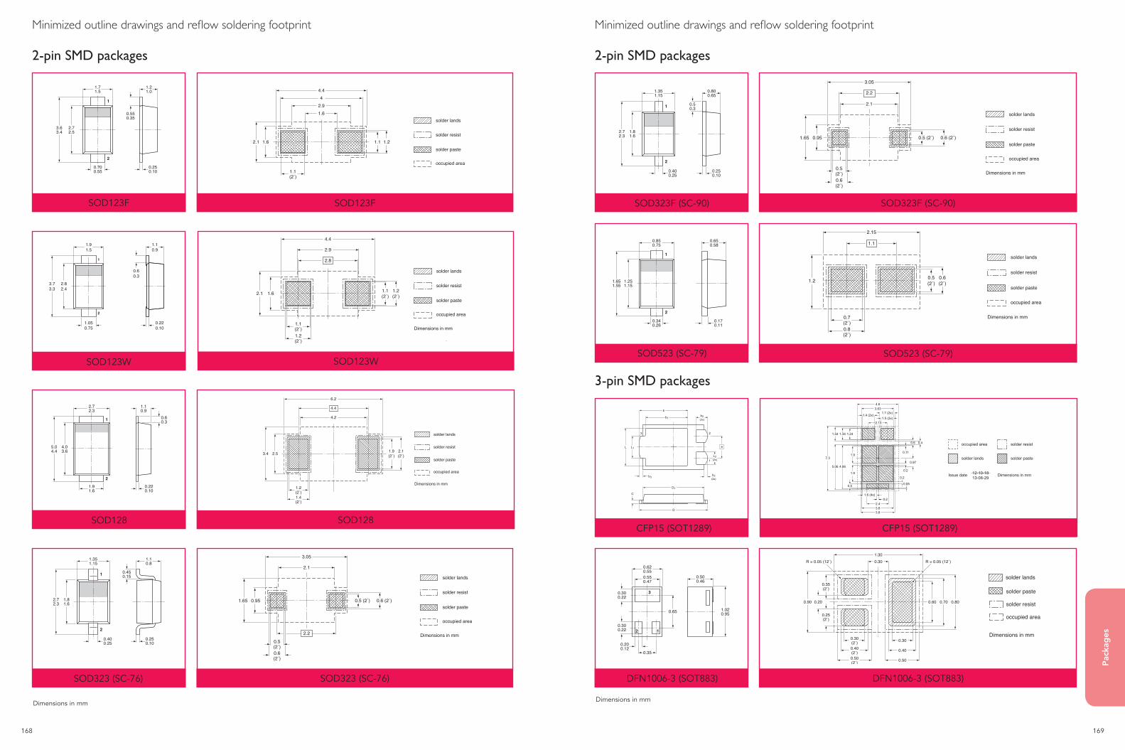
168 169
Pac
kag
es
Minimized outline drawings and reflow soldering footprint
2-pin SMD packages
SOD123F SOD123F
1.6
1.62.94
4.4
1.1 1.22.1
1.1(2´)
solder lands
solder resist
occupied area
solder paste1.6
1.62.94
4.4
1.1 1.22.1
1.1(2´)
solder lands
solder resist
occupied area
solder paste
SOD123W SOD123W
2.9
2.8
4.4
1.62.1 1.2(2´)
1.1(2´)
solder lands
solder resist
occupied area
solder paste
1.1(2´)1.2(2´) sod123w_fr
Dimensions in mm
SOD128
1.10.9
0.220.10
0.60.3
5.04.4
4.03.6
1.91.6
2.72.3
1
2
SOD128
solder lands
solder resist
occupied area
solder paste2.53.4 2.1
(2´)1.9(2´)
4.4
4.2
6.2
1.2(2´)1.4(2´) sod128_fr
Dimensions in mm
Dimensions in mm Dimensions in mm
Minimized outline drawings and reflow soldering footprint
SOD323F (SC-90) SOD323F (SC-90)
0.951.65
2.2
2.1
3.05
solder lands
solder resist
occupied area
solder paste
Dimensions in mm0.5(2´)0.6(2´)
0.6 (2´)0.5 (2´)0.951.65
2.2
2.1
3.05
solder lands
solder resist
occupied area
solder paste
Dimensions in mm0.5(2´)0.6(2´)
0.6 (2´)0.5 (2´)
SOD523 (SC-79) SOD523 (SC-79)
solder lands
solder resist
occupied area
solder paste
Dimensions in mm
0.6(2´)
0.5(2´)
2.15
1.1
0.7(2´)0.8(2´)
1.2
sod523_fr
solder lands
solder resist
occupied area
solder paste
Dimensions in mm
0.6(2´)
0.5(2´)
2.15
1.1
0.7(2´)0.8(2´)
1.2
sod523_fr
2-pin SMD packages
3-pin SMD packages
SOD323 (SC-76) SOD323 (SC-76)
0.951.65
2.2
2.1
3.05
solder lands
solder resist
occupied area
solder paste
0.5(2´)0.6(2´)
0.6 (2´)0.5 (2´)
sod323_fr
Dimensions in mm
CFP15 (SOT1289) CFP15 (SOT1289)
Package outline
© 2010 NXP B.V.All rights reserved. Reproduction in whole or in part is prohibited without prior consent of the copyright owner. The information presented in this document does notform part of any quotation or contract, is believed to be accurate and reliable and may be changed without notice. No liability will be accepted by the publisher for anyconsequence of it’s use. Publication thereof does not convey or imply any license under patent- or other industrial or intellectual property rights.
Printed in the Netherlands
www.nxp.com
ReferencesOutlineversion
Europeanprojection Issue date
IEC JEDEC JEITA
SOT1289
sot1289_po
13-07-1213-08-27
Unit
mmmaxnommin
5.9 4.4 4.711.09 2.05
A
Dimensions (mm are the original dimensions)
Note1. Dimension A is excluding plating thickness.
CFP15: plastic, thermal enhanced ultra thin SMD package; 3 leads; body: 5.8 x 4.3 x 0.78 mm SOT1289
C D
6.6
D1 E e b b1
4.01
b2 b3 L
3.31
L1 L2
1.20.78 0.2 5.8 4.3 2.13 4.616.50.99 1.953.91 3.210.25 1.15.7 4.2 4.516.4
1.19 2.154.11 3.41 1.3
0 2.5 5 mm
scale
3
2
1
1
23
ED1
D
C
b3
L1
b1b2(2x)
b3(2x)
L2(2x)
L
b
A
e
Reflow soldering footprint
© 2010 NXP B.V.All rights reserved. Reproduction in whole or in part is prohibited without prior consent of the copyright owner. The information presented in this document does notform part of any quotation or contract, is believed to be accurate and reliable and may be changed without notice. No liability will be accepted by the publisher for anyconsequence of it’s use. Publication thereof does not convey or imply any license under patent- or other industrial or intellectual property rights.
Printed in the Netherlands
www.nxp.com
2.13
1.6 (4x)
Footprint information for reflow soldering of CFP15 package SOT1289
sot1289_frDimensions in mm
occupied area
solder paste
solder resist
solder lands
Issue date 12-10-1813-08-29
7.3
0.5
1.9
1.9
5.06 4.86
1.24
1.4 (2x)1.7 (2x)
1.5 (2x)
4.63.63
0.11
0.2
0.2
0.22.43.63.8
0.05
0.4
0.97
0.6
1.341.54
DFN1006-3 (SOT883) DFN1006-3 (SOT883)
solder lands
solder paste
solder resist
occupied area
Dimensions in mm
1.300.30R = 0.05 (12´) R = 0.05 (12´)
0.60 0.70 0.800.90
0.30(2´)
0.35(2´)
0.20
0.40(2´)0.50(2´)
0.25(2´)
0.30
0.40
0.50
solder lands
solder paste
solder resist
occupied area
Dimensions in mm
1.300.30R = 0.05 (12´) R = 0.05 (12´)
0.60 0.70 0.800.90
0.30(2´)
0.35(2´)
0.20
0.40(2´)0.50(2´)
0.25(2´)
0.30
0.40
0.50
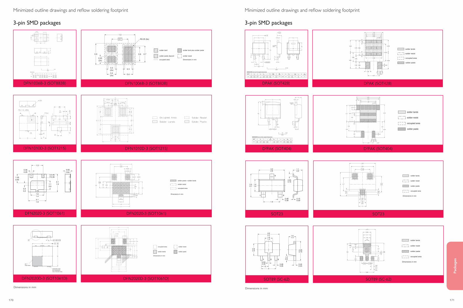
170 171
Pac
kag
es
Dimensions in mm
Minimized outline drawings and reflow soldering footprint Minimized outline drawings and reflow soldering footprint
3-pin SMD packages 3-pin SMD packages
DFN2020-3 (SOT1061)
09-11-12Dimensions in mm
0.65max
2.11.9
1.61.4
0.350.25
0.450.35
2.11.91.1
0.90.30.2
1.050.95
1.3
2
3
1
occupied area
solder paste = solder lands
Dimensions in mm
solder resist
0.4
2.1
1.3
0.25
0.25 0.25
1.1 1.2
0.550.62.3
0.5 (2´)
0.5 (2´) 0.6 (2´)
0.4 (2´)
0.5
1.6
1.7
1.05
occupied area
solder paste = solder lands
Dimensions in mm
solder resist
0.4
2.1
1.3
0.25
0.25 0.25
1.1 1.2
0.550.62.3
0.5 (2´)
0.5 (2´) 0.6 (2´)
0.4 (2´)
0.5
1.6
1.7
1.05
DFN2020-3 (SOT1061)
DFN1006B-3 (SOT883B) DFN1006B-3 (SOT883B)
1.3
0.3
0.6 0.7
0.4
0.9
0.3(2x)0.4(2x)
0.25(2x)
R0.05 (8x)0.7
sot883b_froccupied area
solder land
solder resist
solder land plus solder paste
solder paste deposit
Dimensions in mm
1.3
0.3
0.6 0.7
0.4
0.9
0.3(2x)0.4(2x)
0.25(2x)
R0.05 (8x)0.7
sot883b_froccupied area
solder land
solder resist
solder land plus solder paste
solder paste deposit
Dimensions in mm
Unit
mmmaxnommin
0.400.370.34
0.04 0.550.500.47
0.650.600.55
1.051.000.95
0.650.300.250.22
A(1)
Dimensions
A1 b
0.200.150.12
b1 D E e
0.35
e1 L
0.300.250.22
L1
scale
L (2x)
E
2
3
1
b (2x)
b1
A1A
D
L1
0 0.5 1 mm
e1
e
Unit
mmmaxnommin
0.400.370.34
0.04 0.550.500.47
0.650.600.55
1.051.000.95
0.650.300.250.22
A(1)
Dimensions
A1 b
0.200.150.12
b1 D E e
0.35
e1 L
0.300.250.22
L1
scale
L (2x)
E
2
3
1
b (2x)
b1
A1A
D
L1
0 0.5 1 mm
e1
e
DFN1010D-3 (SOT1215) DFN1010D-3 (SOT1215)
DIMENSIONS (mm are the original dimensions)
A
2
1 3
E1
D2
D1HD
LL1
L2
e1
e
mountingbase
w AMb
E
b2
b1 c
A1
y
0 5 10 mm
scale
UNIT
mm 0.930.46
5.465.00
0.560.20
6.225.98
6.736.47
10.49.6
2.952.55
A1
2.382.22
A b2
1.10.9
b1 e1
0.890.71
b c D1
0.90.5
L2E e
2.285 4.574.0
D2min
4.45
E1min
0.5
L1minHD L w
0.2
ymax
0.2
A
DPAK (SOT428)
6.15
5.805.90
1.80
7.00
1.301.501.401.65
4.57
6.00
6.125
4.725
6.50
0.30
1.00
1.15
5.65
2.302.40
2.453.60
6.00
5.754.60
solder lands
solder resist
occupied area
solder paste
6.15
5.805.90
1.80
7.00
1.301.501.401.65
4.57
6.00
6.125
4.725
6.50
0.30
1.00
1.15
5.65
2.302.40
2.453.60
6.00
5.754.60
solder lands
solder resist
occupied area
solder paste
DPAK (SOT428)
SOT23 SOT23
solder lands
solder resist
occupied area
solder paste
sot023_fr
0.5(3´)0.6(3´)
0.6(3´)
0.7(3´)
3
1
3.3
2.9
1.7
1.9
2
Dimensions in mm
solder lands
solder resist
occupied area
solder paste
sot023_fr
0.5(3´)0.6(3´)
0.6(3´)
0.7(3´)
3
1
3.3
2.9
1.7
1.9
2
Dimensions in mm
UNIT A
mm
A1 D1D
max. E e Lp HD Qc
2.54 2.602.20
15.8014.80
2.902.10
11 1.601.20
10.309.70
4.504.10
1.401.27
0.850.60
0.640.46
b
DIMENSIONS (mm are the original dimensions)
0 2.5 5 mm
scale
e e
E
b
D1
HD
D
Q
Lp
c
A1
A
1 3
2
mountingbase
D2PAK (SOT404) D2PAK (SOT404)
msd057
solder lands
solder resist
occupied area
solder paste
10.50
7.407.50
1.50
1.70
10.60
1.201.301.55
5.08
10.85
0.30
2.15
8.35
2.25
4.60
0.203.00
4.85
7.5
8.15
8.075
8.275
5.40
1.50
msd057
solder lands
solder resist
occupied area
solder paste
10.50
7.407.50
1.50
1.70
10.60
1.201.301.55
5.08
10.85
0.30
2.15
8.35
2.25
4.60
0.203.00
4.85
7.5
8.15
8.075
8.275
5.40
1.50
SOT89 (SC-62) SOT89 (SC-62)
solder lands
solder resist
occupied area
solder paste
sot089_fr
1.21.9
2
2.25
4.75
1(3´)
0.7(3´)
0.6(3´)
1.1(2´)
1.2
0.85 0.2
0.5
1.7
4.85
3.95
4.6
1.51.5
Dimensions in mm
solder lands
solder resist
occupied area
solder paste
sot089_fr
1.21.9
2
2.25
4.75
1(3´)
0.7(3´)
0.6(3´)
1.1(2´)
1.2
0.85 0.2
0.5
1.7
4.85
3.95
4.6
1.51.5
Dimensions in mm
Dimensions in mm
occupied area
solder paste = solder lands
Dimensions in mm
solder resist
0.4
2.1
1.3
0.25
0.25 0.25
1.1 1.2
0.550.62.3
0.5 (2´)
0.5 (2´) 0.6 (2´)
0.4 (2´)
0.5
1.6
1.7
1.05
DFN2020D-3 (SOT1061D)
0.25
occupied area
solder paste
solder resist
solder lands
Issue date
Dimensions in mm
14-03-0514-03-12
0.5 (2x)
0.5 (2x)
0.251
0.35 0.35 0.35
1.1 1.2
0.7 (2x)0.6 (2x)
2.1
1.7
1.3
0.4 (2x)
0.3 (2x)
0.3
0.250.30.351.1
2.32.5
0.4
0.5
1.5
1.6
1.7
0.25
occupied area
solder paste
solder resist
solder lands
Issue date
Dimensions in mm
14-03-0514-03-12
0.5 (2x)
0.5 (2x)
0.251
0.35 0.35 0.35
1.1 1.2
0.7 (2x)0.6 (2x)
2.1
1.7
1.3
0.4 (2x)
0.3 (2x)
0.3
0.250.30.351.1
2.32.5
0.4
0.5
1.5
1.6
1.7
DFN2020D-3 (SOT1061D)
ReferencesOutlineversion
Europeanprojection Issue date
IEC JEDEC JEITA
SOT1061D - - -
sot1061d_po
14-03-1114-03-12
Unit
mmmaxnommin
0.65 0.04 2.1
1.9
1.6
1.4
2.1
1.9
1.1
0.9
0.3
0.2
0.45
0.350.05
A(1)
Dimensions (mm are the original dimensions)
Note1. Dimension A is including plating thickness
A1 bp
0.35
0.25
D D1 E E1 e
1.3
e1 Lp v
0.1
y y1
0.05
0 1 2 mm
scale
pin 1index area
pin 1index area
A BD
E
bp A Bv
e1 2
3
C
yCy1
detail X
A
A1
X
D1
e1
Lp
solderable leadend, protrusionmax. 0.02 mm (3x)
visible depend uponused manufacturingtechnology (6x)
E1
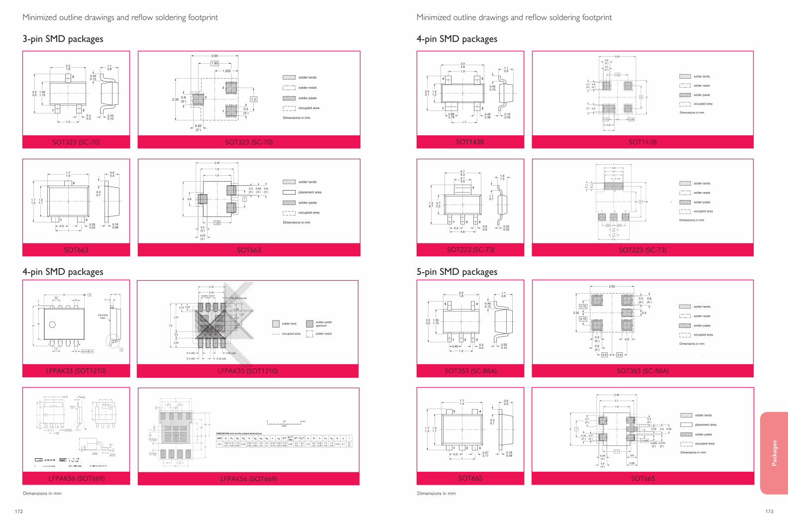
172 173
Pac
kag
es
Minimized outline drawings and reflow soldering footprint Minimized outline drawings and reflow soldering footprint
3-pin SMD packages 4-pin SMD packages
solder lands
placement area
occupied area
solder paste
sot663_fr
2.45
1.6
2 0.8
0.5(3´)
0.5(3´)
0.55(3´)
0.55(3´)
1.9
0.6(3´)
1.65
1
Dimensions in mm
solder lands
placement area
occupied area
solder paste
sot663_fr
2.45
1.6
2 0.8
0.5(3´)
0.5(3´)
0.55(3´)
0.55(3´)
1.9
0.6(3´)
1.65
1
Dimensions in mm
SOT663 SOT663
SOT323 (SC-70)
Dimensions in mm
SOT323 (SC-70)
solder lands
solder resist
occupied area
solder paste
sot323_fr
2.65
2.35 0.6(3´)
0.5(3´)
0.55(3´)
1.325
1.85
1.33
2
1
Dimensions in mm
solder lands
solder resist
occupied area
solder paste
sot323_fr
2.65
2.35 0.6(3´)
0.5(3´)
0.55(3´)
1.325
1.85
1.33
2
1
Dimensions in mm
4-pin SMD packages 5-pin SMD packages
SOT143B
Dimensions in mm
SOT143B
solder lands
solder resist
occupied area
solder paste
sot143b_fr
0.9
0.60.7
3.25
3
0.6(3´)
0.6(3´)0.5(3´)
0.7(3´)
1
1.9
2
0.75 0.95
Dimensions in mm
solder lands
solder resist
occupied area
solder paste
sot143b_fr
0.9
0.60.7
3.25
3
0.6(3´)
0.6(3´)0.5(3´)
0.7(3´)
1
1.9
2
0.75 0.95
Dimensions in mm
SOT223 (SC-73) SOT223 (SC-73)
1.2(4´)
1.2(3´)
1.3(4´)
1.3(3´)
6.15
7
3.85
3.6
3.5
0.3
3.9 7.65
2.3 2.3
6.1
4
2 31
solder lands
solder resist
occupied area
solder paste
Dimensions in mm
1.2(4´)
1.2(3´)
1.3(4´)
1.3(3´)
6.15
7
3.85
3.6
3.5
0.3
3.9 7.65
2.3 2.3
6.1
4
2 31
solder lands
solder resist
occupied area
solder paste
Dimensions in mm
Dimensions in mm Dimensions in mm
LFPAK56 (SOT669) LFPAK56 (SOT669)
0.6(3´)
0.7(4´)
0.25(2´)
0.25(2´)
0.6(4´)
4.2
4.7
0.25(2´)
1.27
1.1
2
3.81
0.9(3´)
SP opening =Cu − 0.050
SR opening =Cu + 0.075
2.15
2.55
3.45 3.5
3.3
solder lands
solder resist occupied area
solder paste125 μm stencil
Dimensions in mm
SOT669Footprint information for reflow soldering
sot669_fr
REFERENCESOUTLINEVERSION
EUROPEANPROJECTION ISSUE DATE
IEC JEDEC JEITA
SOT669 MO-235 06-03-1611-03-25
0 2.5 5 mm
scale
e
E1
b
c2
A2
A2 b cA eUNIT
DIMENSIONS (mm are the original dimensions)
mm 1.100.95
A3A1
0.150.00
1.201.01
0.500.35
b2
4.413.62
b3
2.22.0
b4
0.90.7
0.250.19
c2
0.300.24
4.103.80
6.25.8
H
1.30.8
L2
0.850.40
L
1.30.8
L1
8ϒ0ϒ
w yD(1)
5.04.8
E(1)
3.33.1
E1(1)D1(1)
max
0.25 4.20 1.27 0.25 0.1
1 2 3 4
mountingbase
D1
c
Plastic singleended sracemonted acage (LFPA PowerSO) 4 leads SOT
E
b2
b3
b4
D
2
1
A
A M
12 e
θ
θ
A 3
A
A1
etail
Note1. lastic o metal otusions o 0.15 mm maimum e sie ae not inclue.
0.6(3´)
0.7(4´)
0.25(2´)
0.25(2´)
0.6(4´)
4.2
4.7
0.25(2´)
1.27
1.1
2
3.81
0.9(3´)
SP opening =Cu − 0.050
SR opening =Cu + 0.075
2.15
2.55
3.45 3.5
3.3
solder lands
solder resist occupied area
solder paste125 μm stencil
Dimensions in mm
SOT669Footprint information for reflow soldering
sot669_fr
SOT353 (SC-88A)
Dimensions in mm
SOT353 (SC-88A)
solder lands
solder resist
occupied area
solder paste
sot353_fr
0.4
0.6
0.5(4´)
0.5(4´)
0.6(4´)
0.6(4´)
2.35
2.65
0.90.9
0.75
0.75
Dimensions in mm
SOT665
2.45
2.1
1.6
2 0.25 0.3
0.6
0.65
0.55
0.325(2´)
0.45(4´)
0.4(2´)
0.45(2´)
0.7(2´)
0.5(4´)
0.375(2´)
0.4(5´)
1.7
1
0.538
solder lands
placement area
occupied area
solder paste
Dimensions in mm
SOT665
LFPAK33 (SOT1210) LFPAK33 (SOT1210)occupied area
solder land
solder resist
solder pasteaperture
Notes : 1. Dimensions in mm 2. Stencil Thickness - 125 μm
2.35
2.25
0.4 (x8)
0.3 (x8)
0.65 (x6)
3.9
0.83
0.6
0.75 0.62
2.47
1.05
1.91
0.51
0.51
0.635 0.6170.05 (all around)
0.25 (x6)
occupied area
solder land
solder resist
solder pasteaperture
Notes : 1. Dimensions in mm 2. Stencil Thickness - 125 μm
2.35
2.25
0.4 (x8)
0.3 (x8)
0.65 (x6)
3.9
0.83
0.6
0.75 0.62
2.47
1.05
1.91
0.51
0.51
0.635 0.6170.05 (all around)
0.25 (x6)
ReferencesOutlineversion
Europeanprojection Issue date
IEC JEDEC JEITA
SOT1210
sot1210_po
12-03-1214-04-25
Unit(1)
mmmaxnommin
0.90 0.10 0.35 0.20 0.30 2.700.65
A
Dimensions
Note1. Plastic or metal protrusions of 0.15 mm per side are not included.
A1 b
0.35
b1 c c1 D(1) θD1 E(1) E1 e
0.650.50
e1 H
3.40 2.452.35 3.40
L
0.25
Lp
0.500.20 0.10
w y
3.20 2.000.80 0.00 0.25 0.10 0.20 2.500.25 0°1.90
D2
3.20 0.13 0.30
8°
0 5 mm2.5
scale
Ae1
e X
θ
w A
mountingbase
E1c1b1
b
AE
L
D1
D2
HD
detail X
C cA1
Cy
1 4
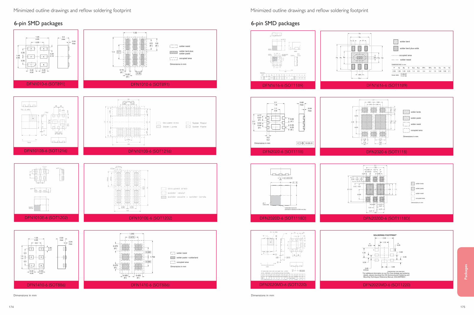
174 175
Pac
kag
es
Minimized outline drawings and reflow soldering footprint
Dimensions in mm
DFN1010-6 (SOT891) DFN1010-6 (SOT891)
sot891_fr
solder resist
occupied area
solder land plussolder paste
Dimensions in mm
0.25(6´)
0.15(6´)
0.5(6´)
0.6(6´)
0.7
0.35
1.4
1.05
sot891_fr
solder resist
occupied area
solder land plussolder paste
Dimensions in mm
0.25(6´)
0.15(6´)
0.5(6´)
0.6(6´)
0.7
0.35
1.4
1.05
6-pin SMD packages6-pin SMD packages
DFN1010B-6 (SOT1216) DFN1010B-6 (SOT1216)
DFN1410-6 (SOT886) DFN1410-6 (SOT886)
sot886_fr
solder resist
occupied area
solder paste = solderland
Dimensions in mm0.425(6´)
1.250
0.675
1.700
0.325(6´)
0.270(6´)
0.370(6´)
0.500
0.500
sot886_fr
solder resist
occupied area
solder paste = solderland
Dimensions in mm0.425(6´)
1.250
0.675
1.700
0.325(6´)
0.270(6´)
0.370(6´)
0.500
0.500
DFN1010E-6 (SOT1202)
Package outline
© 2010 NXP B.V.All rights reserved. Reproduction in whole or in part is prohibited without prior consent of the copyright owner. The information presented in this document does notform part of any quotation or contract, is believed to be accurate and reliable and may be changed without notice. No liability will be accepted by the publisher for anyconsequence of it’s use. Publication thereof does not convey or imply any license under patent- or other industrial or intellectual property rights.
Printed in the Netherlands
www.nxp.com
ReferencesOutlineversion
Europeanprojection Issue date
IEC JEDEC JEITA
SOT1202
sot1202_po
10-04-0210-04-06
Unit
mmmaxnommin
0.35 0.04 1.051.000.95
1.051.000.95
0.55 0.350.400.350.32
A(1)
Dimensions
Note1. Including plating thickness.2. Visible depending upon used manufacturing technology.
XSON6: extremely thin small outline package; no leads;6 terminals; body 1.0 x 1.0 x 0.35 mm SOT1202
A1 b
0.200.150.12
D E e e1 L
0.350.300.27
L1
0 0.5 1 mm
scale
terminal 1index area
D
E
(4´)(2)
e1 e1
e
L
b1 2 3
L1
6 5 4
(6´)(2)
AA1
DFN1010E-6 (SOT1202)
Minimized outline drawings and reflow soldering footprint
Dimensions in mm
DFN1616-6 (SOT1189) DFN1616-6 (SOT1189)
Unit(1)
mmmaxnommin
0.5 0.05
0.00
0.300.250.20
1.71.61.5
1.31.21.1
1.71.61.5
0.5 10.350.300.25
0.05
A
Dimensions
A1 A3
0.127
b D Dh E Eh
0.60.50.4
e e1 k
0.2
L v
0.1
w
0.05
y
0.05
y1
0 1 2 mm
scale
D
E
B A
terminal 1index area
X
detail X
A
A1A3
C
yCy1
Dh
Eh
k
L
b
e1
e AC BvCw
terminal 1index area
46
31
DIMENSIONS in mm
By
1.05
P
0.50
Ay
1.85
solder land plus solder paste
occupied area
D P
Hx
Gx
SPx
GyHy
SLx
Ay By
SLx SLyD
0.25 1.3 0.8
SPx
0.4
Gx Gy Hx Hy
1.5 1.85 1.85 2.1
SPy
0.2
SLySPy
solder land
solder resist
Issue date 11-06-2711-07-06
DIMENSIONS in mm
By
1.05
P
0.50
Ay
1.85
solder land plus solder paste
occupied area
D P
Hx
Gx
SPx
GyHy
SLx
Ay By
SLx SLyD
0.25 1.3 0.8
SPx
0.4
Gx Gy Hx Hy
1.5 1.85 1.85 2.1
SPy
0.2
SLySPy
solder land
solder resist
Issue date 11-06-2711-07-06
DIMENSIONS in mm
By
1.05
P
0.50
Ay
1.85
solder land plus solder paste
occupied area
D P
Hx
Gx
SPx
GyHy
SLx
Ay By
SLx SLyD
0.25 1.3 0.8
SPx
0.4
Gx Gy Hx Hy
1.5 1.85 1.85 2.1
SPy
0.2
SLySPy
solder land
solder resist
Issue date 11-06-2711-07-06
DFN2020-6 (SOT1118)
10-05-31Dimensions in mm
0.04max
0.65max
0.770.57(2´)0.540.44(2´)
2.11.9
2.11.9
1.10.9
0.30.2
0.65(4´)
0.350.25(6´)
43
1 6
DFN2020-6 (SOT1118)
Dimensions in mm
solder paste
solder resist
occupied area
solder lands
0.49 0.490.650.65
0.875
0.875
2.25
0.35(6´)
0.3(6´)
0.4(6´)
0.45(6´)
0.72(2´)0.82(2´)
1.05(2´)
1.15(2´)
2.1
DFN2020D-6 (SOT1118D)
ReferencesOutlineversion
Europeanprojection Issue date
IEC JEDEC JEITA
SOT1118D - - -
sot1118d_po
14-07-1614-10-16
Unit
mmmaxnommin
0.650.620.59
0.04 2.1 0.77 2.1 1.0 0.54 0.300.49 0.250.44 0.20
0.05
A
Dimensions (mm are the original dimensions)
Note1. Dimension A is including plating thickness.
A1 bp
0.352.0 0.67 2.0 0.90.301.9 0.57 1.9 0.80.25
D D1 E E1 e
0.65
e1 Lp v
0.1
y y1
0.05
0 1 2 mm
scale
pin 1index area
cut-off end ofnon-fuctional bonding wire
A BD
E
detail X
A1
A
E1(2x)
Lp(6x)
e1 e1
pin 1index area
D1(2x)
1 3
6 4
bp(6x)
BAv
X
C
yCy1
(8x)
solderable lead endprotrusion maximum 0.035 mm (6x)
e e
DFN2020D-6 (SOT1118D)
0.33
solder lands
occupied area
solder resist
solder paste
Dimensions in mm
0.9 1 1.1
0.350.45 0.2
1.652.2
0.30.25 0.65
1.650.21
0.31
0.935
0.22
2.32.5
0.12
0.53 0.43
0.77
0.670.570.49
DFN2020MD-6 (SOT1220) DFN2020MD-6 (SOT1220)
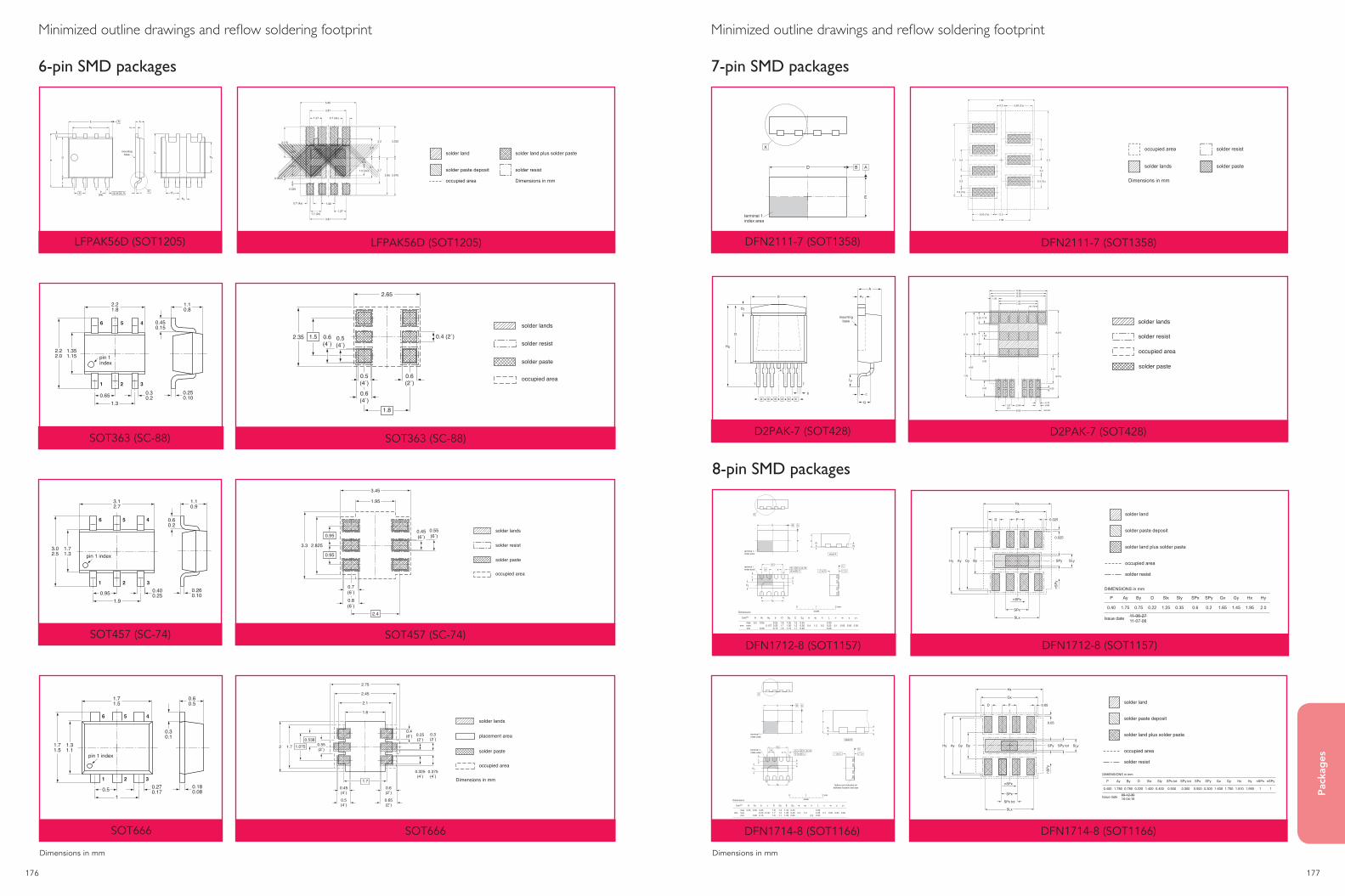
176 177
Pac
kag
es
Minimized outline drawings and reflow soldering footprint
7-pin SMD packages
Dimensions in mmDimensions in mm
SOT363 (SC-88) SOT363 (SC-88)
solder lands
solder resist
occupied area
solder paste
sot363_fr
2.65
2.35 0.4 (2´)
0.6(2´)
0.5(4´)
0.5(4´)
0.6(4´)
0.6(4´)
1.5
1.8
Dimensions in mm
SOT457 (SC-74) SOT457 (SC-74)
solder lands
solder resist
occupied area
solder paste
sot457_fr
3.45
1.95
2.8253.3
0.45(6´)
0.55(6´)
0.7(6´)0.8(6´)
2.4
0.95
0.95
Dimensions in mm
SOT666 SOT666
solder lands
placement area
occupied area
solder paste
sot666_fr
2.75
2.45
2.1
1.6
0.4(6´)
0.55(2´)
0.25(2´)
0.6(2´)
0.65(2´)
0.3(2´)
0.325(4´)
0.45(4´)
0.5(4´)
0.375(4´)
1.72
1.7
1.0750.538
Dimensions in mm
8-pin SMD packages
DFN1712-8 (SOT1157) DFN1712-8 (SOT1157)
SOT1157-1
DIMENSIONS in mm
Footprint information for reflow soldering of HXSON8 package
Generic footprint patternRefer to the package outline drawing for actual layout
By D Slx Sly Gx Gy Hx Hy
0.75 0.22 1.25 0.35
P
0.40
Ay
1.75 1.65 1.45 1.95 2.0
SPx SPy
0.6 0.2
solder land plus solder paste
occupied area
solder land
solder paste deposit
solder resist
D P
Gx
Gy
Hx
Hy SPy SLyByAy
nSP
y
nSPx
SPx
SLx
0.025
0.025
sot1157-1_frIssue date 11-06-2711-07-06
Minimized outline drawings and reflow soldering footprint
6-pin SMD packages
LFPAK56D (SOT1205)
Package outline
© 2010 NXP B.V.All rights reserved. Reproduction in whole or in part is prohibited without prior consent of the copyright owner. The information presented in this document does notform part of any quotation or contract, is believed to be accurate and reliable and may be changed without notice. No liability will be accepted by the publisher for anyconsequence of it’s use. Publication thereof does not convey or imply any license under patent- or other industrial or intellectual property rights.
Printed in the Netherlands
www.nxp.com
ReferencesOutlineversion
Europeanprojection Issue date
IEC JEDEC JEITA
SOT1205
sot1205_po
13-02-1913-02-21
Unit
mmmaxnommin
1.05 0.1
0.0
4.4
4.1
0.25
0.19
0.30
0.24
4.70
4.453.5
5.30
4.95
0.85 0.85
0.40
A
Dimensions
Note1. Plastic or metal protrusions of 0.2 mm maximum per side are not included.
Plastic single ended surface mounted package (LFPAK56D); 8 leads SOT1205
A1 b
0.50
0.35
b1 c c1 D(1)
0.18°
0°
y θD1(1)
4.8
D2(ref) E(1) E1(1)
1.8
1.6
E2 e
1.27
H
6.2
5.9
L
1.3
0.8
L1
0.55
0.30
Lp
0.25
w
0 2.5 5 mm
scale
detail X
A1 C
Lp
θ
Cy
E2
D2
E1
D1mounting
base
c X
A
c1
A
e b(8x) w A
D
E
H
L
L1
b1
1 2 3 4
LFPAK56D (SOT1205)
Reflow soldering footprint
© 2010 NXP B.V.All rights reserved. Reproduction in whole or in part is prohibited without prior consent of the copyright owner. The information presented in this document does notform part of any quotation or contract, is believed to be accurate and reliable and may be changed without notice. No liability will be accepted by the publisher for anyconsequence of it’s use. Publication thereof does not convey or imply any license under patent- or other industrial or intellectual property rights.
Printed in the Netherlands
www.nxp.com
SOT1205Footprint information for reflow soldering of LFPAK56D package
sot1205_froccupied area
solder land
solder resist
solder land plus solder paste
solder paste deposit
Dimensions in mm
Reflow soldering footprint
© 2010 NXP B.V.All rights reserved. Reproduction in whole or in part is prohibited without prior consent of the copyright owner. The information presented in this document does notform part of any quotation or contract, is believed to be accurate and reliable and may be changed without notice. No liability will be accepted by the publisher for anyconsequence of it’s use. Publication thereof does not convey or imply any license under patent- or other industrial or intellectual property rights.
Printed in the Netherlands
www.nxp.com
1.27 0.7 (4x)
SOT1205Footprint information for reflow soldering of LFPAK56D package
sot1205_froccupied area
solder land
solder resist
solder land plus solder paste
solder paste deposit
Dimensions in mm
5.85
0.8
2.0
1.0 (2x)2.1
3.2 3.325
2.7
3.85 3.975
1.275
3.175
1.875
0.0625
0.025
3.81
3.81
1.44
1.271.1 (2x)
0.7 (4x)
ReferencesOutlineversion
Europeanprojection Issue date
IEC JEDEC JEITA
SOT1358-1 - - -MO-252- - -
sot1358-1_po
13-08-2113-09-12
Unit(1)
mmmaxnommin
0.5 0.05 0.25 2.20 1.20.4
A
Dimensions (mm are the original dimensions)
Note1. Plastic or metal protrusions of 0.075 mm maximum per side are not included.
A1 b
0.127
DA3
0.05 0.051.0 0.10.20 2.10 1.1 0.5 0.1 0.050.2 0.30.00 0.15 2.05 1.0
0.5
0 1 2 mm
scale
X
E y y1k L L1 v we e1
1.5
e2
B AD
E
C
yCy1
AA1
A3
e
L1
b AC BvCw
e2
e1
1 4
L
k
terminal 1index area
terminal 1index area
57
DFN2111-7 (SOT1358) DFN2111-7 (SOT1358)
DFN1714-8 (SOT1166)
Unit(1)
mmmaxnommin
0.55 0.05
0.00
0.250.200.15
1.81.71.6
1.31.21.1
1.451.351.25
0.4 1.20.300.250.20
0.05
A
Dimensions
A1 c
0.127
b D Dh E Eh
0.450.400.35
e e1 k
0.2
L v
0.1
w
0.05
y
0.05
y1
0 1 2 mm
scale
X
C
yCy1
tiebars are indicated onarbitrary location and size
detail X
A
A1c
terminal 1index area
B AD
E
bterminal 1index area
e1e AC Bv
Cw
L
k
Eh
Dh
1
8
4
5
DFN1714-8 (SOT1166)
DIMENSIONS in mm
Generic footprint patternRefer to the package outline drawing for actual layout
By D Slx Sly Gx Gy Hx Hy
0.780 0.220 1.400 0.400
P
0.400
Ay
1.780 1.630 1.700 1.910 1.990
SPx SPy
0.500
SPx tot
0.500 0.300
nSPx nSPy
1 1
SPy tot
0.300
solder land plus solder paste
occupied area
solder land
solder paste deposit
solder resist
D P
Gx
Gy
Hx
Hy SPy SPy tot SLyByAy
nSPy
nSPx
SPx tot
SPx
SLx
0.05
0.05
Issue date 09-12-3010-04-16
D2PAK-7 (SOT428) D2PAK-7 (SOT428)
ReferencesOutlineversion
Europeanprojection Issue date
IEC JEDEC JEITA
SOT427
sot427_po
06-03-1612-10-16
Unit(1)
mmmaxnommin
4.5
4.1
1.40
1.27
0.64
0.46
11 1.6
1.2
10.3
9.7
2.90
2.10
15.8
14.8
2.6
2.2
A
Dimensions (mm are the original dimensions)
A1 b
0.85
0.60
c D D1 E e
1.27
Lp HD Q
0 2.5 5 mm
scale
e e e eee
E
b
A1
A
1
4
7
mountingbase
D1
HD
D
Q
Lp
c
handbook, full pagewidth
MSD059
solder lands
solder resist
occupied area
solder paste
10.50
7.407.50
1.50
1.70
10.60
8.92
0.700.801.27
(4×)2.54
10.85
0.30
2.15
8.35
2.25
4.60
0.203.00
4.85
7.95
8.15
8.075
8.275
5.40
1.50
Dimensions in mm.
handbook, full pagewidth
MSD059
solder lands
solder resist
occupied area
solder paste
10.50
7.407.50
1.50
1.70
10.60
8.92
0.700.801.27
(4×)2.54
10.85
0.30
2.15
8.35
2.25
4.60
0.203.00
4.85
7.95
8.15
8.075
8.275
5.40
1.50
Dimensions in mm.
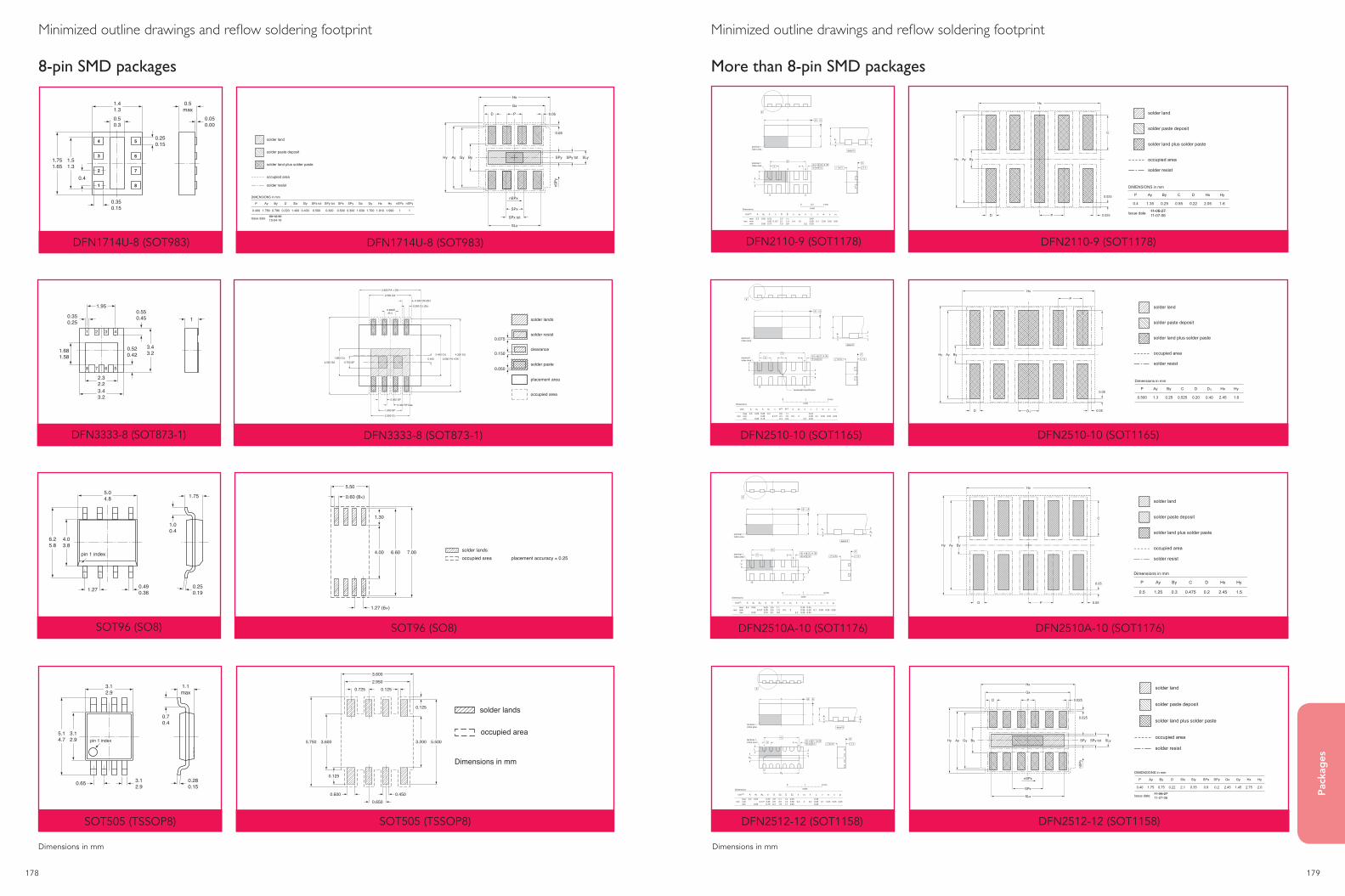
178 179
Pac
kag
es
Minimized outline drawings and reflow soldering footprint
More than 8-pin SMD packages
SOT505 (TSSOP8) SOT505 (TSSOP8)
occupied area
solder lands
Dimensions in mm
3.2003.6005.750
0.725
0.650
0.125
0.4500.600
3.600
2.950
0.125
0.125
5.500
DFN2110-9 (SOT1178) DFN2110-9 (SOT1178)
Unit(1)
mmmaxnommin
0.5 0.05
0.000.127
2.22.12.0
1.11.00.9
0.40.2
0.430.380.33
0.05
A
Dimensions
A1 b
0.250.200.15
c D E e e1
1.6
k L v
0.1
w y
0.05
y1
0.05
0 0.5 1 mm
scale
terminal 1index area
B AD
E
X
C
yCy1
terminal 1index area b
e1
e AC BvCw
L
k
1 3 5
9 6
detail X
AA1
c
DFN2510-10 (SOT1165) DFN2510-10 (SOT1165)
SOT1165-1
Remark:Stencil of 75 μm is recommended.A stencil of 75 μm gives an aspect ratio of 0.77With a stencil of 100 μm one will obtain an aspect ratio of 0.58
Footprint information for reflow soldering of XSON10 package
solder land plus solder paste
occupied area
solder land
solder paste deposit
solder resist
Dimensions in mm
Ay By C D Hy
1.3 0.25 0.525 0.20
D1
0.40
P
0.500 1.6
Hx
2.45
Generic footprint patternRefer to the package outline drawing for actual layout
sot1165-1_fr
Hx
ByHy
0.05
C
P
D 0.05D1
Ay
Unit
mmmaxnommin
0.5 0.05
0.00
0.250.200.15
0.4 2.62.52.4
1.11.00.9 0.2
0.430.380.33
0.05
A
Dimensions
A1 c
0.127
b b1 D(1) E(1) e
0.5
e1
2
k L v
0.1
w y
0.05
y1
0.05
0 1 2 mm
scale
X
C
yCy1
B A
terminal 1index area
D
E
detail X
A
cA1
b
k
L
b1
e1
e AC BvCwterminal 1
index area
10 6Terminal#3 identification
51
SOT1165-1
Remark:Stencil of 75 μm is recommended.A stencil of 75 μm gives an aspect ratio of 0.77With a stencil of 100 μm one will obtain an aspect ratio of 0.58
Footprint information for reflow soldering of XSON10 package
solder land plus solder paste
occupied area
solder land
solder paste deposit
solder resist
Dimensions in mm
Ay By C D Hy
1.3 0.25 0.525 0.20
D1
0.40
P
0.500 1.6
Hx
2.45
Generic footprint patternRefer to the package outline drawing for actual layout
sot1165-1_fr
Hx
ByHy
0.05
C
P
D 0.05D1
Ay
DFN2510A-10 (SOT1176) DFN2510A-10 (SOT1176)
Unit(1)
mmmaxnommin
0.5 0.05
0.00
0.250.200.15
2.62.52.4
1.11.00.9
0.50.2
0.400.350.30
0.1
A
Dimensions
A1 A3
0.127
b D E e e1
2
k L L1
0.450.400.35
v w
0.05
y
0.05
y1
0.05
0 1 2 mm
scale
X
C
yCy1
terminal 1index area
B AD
E
detail X
A1
A
A3
b
k
L
L1
terminal 1index area
e1
e AC BvCw
10 6
51
8-pin SMD packages
Generic footprint pattern. Refer to the package outline drawing for actual layout.
DFN1714U-8 (SOT983) DFN1714U-8 (SOT983)
DIMENSIONS in mm
Generic footprint patternRefer to the package outline drawing for actual layout
By D Slx Sly Gx Gy Hx Hy
0.780 0.220 1.400 0.400
P
0.400
Ay
1.780 1.630 1.700 1.910 1.990
SPx SPy
0.500
SPx tot
0.500 0.300
nSPx nSPy
1 1
SPy tot
0.300
solder land plus solder paste
occupied area
solder land
solder paste deposit
solder resist
D P
Gx
Gy
Hx
Hy SPy SPy tot SLyByAy
nSPy
nSPx
SPx tot
SPx
SLx
0.05
0.05
Issue date 09-12-3010-04-16
Minimized outline drawings and reflow soldering footprint
DFN3333-8 (SOT873-1)
09-02-03Dimensions in mm
1
2.32.2
1.681.58
0.550.45
0.520.42
3.43.2
3.43.2
1.95
0.350.25
1 2 3 4
8 7 6 5
DFN3333-8 (SOT873-1)
SOT873-1
Dimensions in mm
Footprint information for reflow soldering of HVSON8 package
0.075
solder lands
solder resist
placement area
solder paste
clearance
occupied area
0.050
0.150
0.650(6×)
0.4000.700 SP4.550 OA
1.600 CU2.400 CU 4.300 CU
3.600 PA +OA
2.500 OA
3.600 PA + OA
2.300 CU
1.400 SP
0.300 CU (×)
0.550 OA (×)
0.500 SP
0.400 SP ap
SOT96 (SO8) SOT96 (SO8)sot096-1_froccupied area
solder landsDimensions in mmplacement accuracy ± 0.25
1.30
0.60 (8×)
1.27 (6×)
4.00 6.60
5.50
7.00sot096-1_froccupied area
solder landsDimensions in mmplacement accuracy ± 0.25
1.30
0.60 (8×)
1.27 (6×)
4.00 6.60
5.50
7.00
Dimensions in mm Dimensions in mm
DFN2512-12 (SOT1158) DFN2512-12 (SOT1158)
SOT1158-1
DIMENSIONS in mm
Footprint information for reflow soldering of HXSON12 package
By D Slx Sly Gx Gy Hx Hy
0.75 0.22 2.1 0.35
P
0.40
Ay
1.75 2.45 1.45 2.75 2.0
SPx SPy
0.9 0.2
solder land plus solder paste
occupied area
solder land
solder paste deposit
solder resist
sot1158-1_fr
Generic footprint patternRefer to the package outline drawing for actual layout
D P
Gx
Gy
Hx
Hy SPy SPy tot SLyByAy
nSP
y
nSPx
SPx
SLx
0.025
0.025
Issue date 11-06-2711-07-06
Unit(1)
mmmaxnommin
0.5 0.05
0.00
0.250.200.15
2.62.52.4
2.12.01.9
1.31.21.1
0.4 20.300.250.20
0.05
A
Dimensions
A1 A3
0.127
b D D2 E E2
0.350.300.25
e e1 k
0.2
L v
0.1
w
0.05
y
0.05
y1
0 1 2 mm
scale
X
C
yCy1b
e1
e AC BvCw
terminal 1index area
D2
E2
L
k
12 7
1 6
B A
terminal 1index area
D
E
detail X
AA1
A3
SOT1158-1
DIMENSIONS in mm
Footprint information for reflow soldering of HXSON12 package
By D Slx Sly Gx Gy Hx Hy
0.75 0.22 2.1 0.35
P
0.40
Ay
1.75 2.45 1.45 2.75 2.0
SPx SPy
0.9 0.2
solder land plus solder paste
occupied area
solder land
solder paste deposit
solder resist
sot1158-1_fr
Generic footprint patternRefer to the package outline drawing for actual layout
D P
Gx
Gy
Hx
Hy SPy SPy tot SLyByAy
nSP
y
nSPx
SPx
SLx
0.025
0.025
Issue date 11-06-2711-07-06
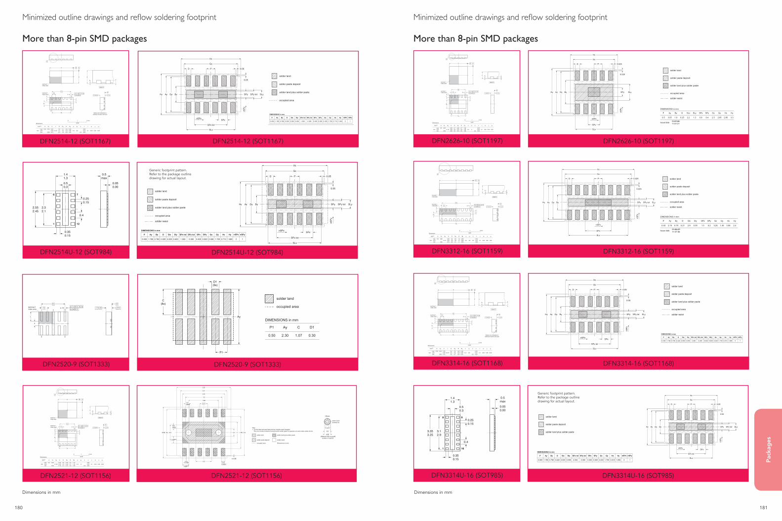
180 181
Pac
kag
es
Minimized outline drawings and reflow soldering footprint
More than 8-pin SMD packages
DFN2521-12 (SOT1156)
Unit(1)
mmmaxnommin
0.5 0.05
0.00
0.250.200.15
2.62.52.4
2.252.202.15
2.22.12.0
0.4 20.300.250.20
0.05
A
Dimensions
A1 A3
0.127
b D Dh E Eh
1.151.101.05
e e1 k
0.2
L v
0.1
w
0.05
y
0.05
y1
0 1 2 mm
scale
X
B A
terminal 1index area
D
E
detail X
AA1
A3
C
yCy1b
terminal 1index area
e1
e AC BvCw
L
Eh
k
Dh
61
712
sot1156-1_froccupied area
solder land
solder resist
solder land plus solder paste
solder paste deposit
Dimensions in mm
Note1. On the heat sink pad there are four double mask triangles. This is to create a stand off and prevents solder paste to squeeze out and create solder shorts.
0.40.4
0.4
1.
1.
0. 0.4 1.1 1. .4
0.01
.4.
0.1
0.1
0.0.01 0.1
1
.
.
.4
0.
0.
side
solder resistcovered via
0.side full covered
number of vias
DFN2521-12 (SOT1156)
sot1156-1_froccupied area
solder land
solder resist
solder land plus solder paste
solder paste deposit
Dimensions in mm
Note1. On the heat sink pad there are four double mask triangles. This is to create a stand off and prevents solder paste to squeeze out and create solder shorts.
0.40.4
0.4
1.
1.
0. 0.4 1.1 1. .4
0.01
.4.
0.1
0.1
0.0.01 0.1
1
.
.
.4
0.
0.
side
solder resistcovered via
0.side full covered
number of vias
DFN2626-10 (SOT1197) DFN2626-10 (SOT1197)
Unit(1)
mmmaxnommin
0.5 0.05
0.00
0.300.250.20
2.72.62.5
2.202.152.10
2.72.62.5
0.5 20.400.350.30
0.05
A
Dimensions
A1 A3
0.127
b D Dh E Eh
1.301.251.20
e e1 k
0.2
L v
0.1
w
0.05
y
0.05
y1
0 1 2 mm
scale
C
yCy1
X
D
E
B A
terminal 1index area
detail X
A A1A3
Dh
Eh
k
L
b
e1
e AC BvCw
terminal 1index area
51
610
DFN3312-16 (SOT1159) DFN3312-16 (SOT1159)
Unit(1)
mmmaxnommin
0.5 0.05
0.00
0.250.200.15
3.43.33.2
2.92.82.7
1.31.21.1
0.4 2.80.300.250.20
0.05
A
Dimensions
A1 A3
0.127
b D D2 E E2
0.350.300.25
e e1 k
0.2
L v
0.1
w
0.05
y
0.05
y1
0 1 2 mm
scale
X
C
yCy1b
e1
e AC BvCw
terminal 1index area
D2
E2
L
k
16 9
1 8
B A
terminal 1index area
D
E
detail X
AA1
A3
DIMENSIONS in mm
By D Slx Sly Gx Gy Hx Hy
0.75 0.21 2.9 0.35
P
0.40
Ay
2.15 3.25 1.45 3.55 2.4
SPx SPy
1.3 0.2
solder land plus solder paste
occupied area
solder land
solder paste deposit
solder resist
Generic footprint patternRefer to the package outline drawing for actual layout
D P
Gx
Gy
Hx
Hy SPy SPy tot SLyByAy
nSP
y
nSPx
SPx
SLx
0.025
0.025
Issue date 11-06-2711-07-06
DFN3314-16 (SOT1168) DFN3314-16 (SOT1168)
Unit(1)
mmmaxnommin
0.55 0.05
0.00
0.250.200.15
3.43.33.2
2.92.82.7
1.451.351.25
0.4 2.80.300.250.20
0.05
A
Dimensions
A1 c
0.127
b D Dh E Eh
0.450.400.35
e e1 k
0.2
L v
0.1
w
0.05
y
0.05
y1
0 1 2 mm
scale
X
C
yCy1
tiebars are indicated onarbitrary location and size
detail X
A
A1c
terminal 1index area
B AD
E
bterminal 1index area
e1e AC Bv
Cw
L
k
Eh
Dh
1
16
8
9
SOT985-1
DIMENSIONS in mm
Footprint information for reflow soldering of HXSON16 package
Generic footprint patternRefer to the package outline drawing for actual layout
By D Slx Sly Gx Gy Hx Hy
0.780 0.220 3.000 0.400
P
0.400
Ay
1.780 3.230 1.700 3.510 1.990
SPx SPy
0.350 0.300
nSPx nSPy
3 1
SPx tot SPy tot
2.350 0.300
solder land plus solder paste
occupied area
solder land
solder paste deposit
solder resist
D P
Gx
Gy
Hx
Hy
SPx
SPy SPy tot SLyByAy
nSPy
nSPx
SPx tot
SLx
0.05
0.05
Minimized outline drawings and reflow soldering footprint
Dimensions in mm Dimensions in mm
DFN2514-12 (SOT1167)DFN2514-12 (SOT1167)
Unit(1)
mmmaxnommin
0.55 0.05
0.00
0.250.200.15
2.62.52.4
2.12.01.9
1.451.351.25
0.4 2.00.300.250.20
0.05
A
Dimensions
A1 c
0.127
b D Dh E Eh
0.450.400.35
e e1 k
0.2
L v
0.1
w
0.05
y
0.05
y1
0 1 2 mm
scale
X
C
yCy1
tiebars are indicated onarbitrary location and size
detail X
A
A1c
terminal 1index area
B AD
E
bterminal 1index area
e1e AC Bv
Cw
L
k
Eh
Dh
1
12
6
7
SOT984-1
DIMENSIONS in mm
Footprint information for reflow soldering of HXSON12 package
Generic footprint patternRefer to the package outline drawing for actual layout
By D Slx Sly Gx Gy Hx Hy
0.780 0.220 2.200 0.400
P
0.400
Ay
1.780 2.430 1.700 2.710 1.990
SPx SPy
0.400 0.300
nSPx nSPy
2 1
SPx tot SPy tot
1.500 0.300
solder land plus solder paste
occupied area
solder land
solder paste deposit
solder resist
D P
Gx
Gy
Hx
Hy
SPx
SPy SPy tot SLyByAy
nSPy
nSPx
SPx tot
SLx
0.05
0.05
More than 8-pin SMD packages
DFN2514U-12 (SOT984) DFN2514U-12 (SOT984)
SOT984-1
DIMENSIONS in mm
Footprint information for reflow soldering of HXSON12 package
Generic footprint patternRefer to the package outline drawing for actual layout
By D Slx Sly Gx Gy Hx Hy
0.780 0.220 2.200 0.400
P
0.400
Ay
1.780 2.430 1.700 2.710 1.990
SPx SPy
0.400 0.300
nSPx nSPy
2 1
SPx tot SPy tot
1.500 0.300
solder land plus solder paste
occupied area
solder land
solder paste deposit
solder resist
D P
Gx
Gy
Hx
Hy
SPx
SPy SPy tot SLyByAy
nSPy
nSPx
SPx tot
SLx
0.05
0.05
Generic footprint pattern. Refer to the package outline drawing for actual layout.
DFN2520-9 (SOT1333) DFN2520-9 (SOT1333)
Package outline
© 2010 NXP B.V.All rights reserved. Reproduction in whole or in part is prohibited without prior consent of the copyright owner. The information presented in this document does notform part of any quotation or contract, is believed to be accurate and reliable and may be changed without notice. No liability will be accepted by the publisher for anyconsequence of it’s use. Publication thereof does not convey or imply any license under patent- or other industrial or intellectual property rights.
Printed in the Netherlands
www.nxp.com
e1
ReferencesOutlineversion
Europeanprojection Issue date
IEC JEDEC JEITA
SOT1333-1 MO-252
sot1333-1_po
12-09-2513-05-01
Unit(1)
mmmaxnommin
0.5 0.05
0.00
A
Dimensions (mm are the original dimensions)
DFN2520-9: plastic extremely thin small outline package; no leads; 9 terminals; body 2 x 2.5 x 0.5 mm SOT1333-1
A1
0.250.200.15
2.12.01.9
0.90.80.7
2.62.52.4
0.5 2.00.2
b c
0.152
0.050
D E e e1 k L v
0.050.1
w y
0.05
y1
0.05
0 3 mm21scale
X
L
k
Note1. Plastic or metal protrusions of 0.075 mm maximum per side are not included.
terminal 1index area
terminal 1index area
B AD
E
9 6
e1 3
b5
AC BvCw
detail X
c
AA1
C
yCy1
- - - - - -
Reflow soldering footprint
© 2010 NXP B.V.All rights reserved. Reproduction in whole or in part is prohibited without prior consent of the copyright owner. The information presented in this document does notform part of any quotation or contract, is believed to be accurate and reliable and may be changed without notice. No liability will be accepted by the publisher for anyconsequence of it’s use. Publication thereof does not convey or imply any license under patent- or other industrial or intellectual property rights.
Printed in the Netherlands
www.nxp.com
Footprint information for reflow soldering of DFN2520-9 package SOT1333-1
sot1333-1_fr
occupied area
Dimensions in mm13-05-0813-05-21
solder land
DIMENSIONS in mm
Ay D1P1
2.30 1.07 0.30
C
0.50
P1
Ay
D1(9x)
C(8x)
DFN3314U-16 (SOT985) DFN3314U-16 (SOT985)
SOT985-1
DIMENSIONS in mm
Footprint information for reflow soldering of HXSON16 package
Generic footprint patternRefer to the package outline drawing for actual layout
By D Slx Sly Gx Gy Hx Hy
0.780 0.220 3.000 0.400
P
0.400
Ay
1.780 3.230 1.700 3.510 1.990
SPx SPy
0.350 0.300
nSPx nSPy
3 1
SPx tot SPy tot
2.350 0.300
solder land plus solder paste
occupied area
solder land
solder paste deposit
solder resist
D P
Gx
Gy
Hx
Hy
SPx
SPy SPy tot SLyByAy
nSPy
nSPx
SPx tot
SLx
0.05
0.05
Generic footprint pattern. Refer to the package outline drawing for actual layout.
182 183
Pac
kag
es
Minimized outline drawings and reflow soldering footprint
Dimensions in mm
More than 8-pin SMD packages
SOT163 (SO20) SOT163 (SO20)sot163-1_froccupied area
solder landsDimensions in mmplacement accuracy ± 0.25
.50
0.0 20×
.2 ×
.00 .00
.0
.0sot163-1_froccupied areasolder lands
Dimensions in mmplacement accuracy ± 0.25
.50
0.0 20×
.2 ×
.00 .00
.0
.0
SOT337 (SSOP14)UNIT A1 A2 A3 bp c D(1) E (1) e HE L Lp Q Zywv θ
REFERENCESOUTLINEVERSION
EUROPEANPROJECTION ISSUE DATE
IEC JEDEC JEITA
mm 0.210.05
1.801.65 0.25 0.38
0.250.200.09
6.46.0
5.45.2 0.65 1.25 0.27.9
7.61.030.63
0.90.7
1.40.9
80
oo0.13 0.1
DIMENSIONS (mm are the original dimensions)
Note1. Plastic or metal protrusions of 0.25 mm maximum per side are not included.
SOT337-1 99-12-2703-02-19
(1)
w Mbp
D
HE
E
Z
e
c
v M A
XA
y
1 7
14 8
θ
AA1A2
p
detail X
A 3
MO-150
pin 1 index
0 2.5 5 mm
scale
SSOP1 plastic shrin small otline pacage 1 leads body width 3 mm SOT331
Ama
2
UNIT A1 A2 A3 bp c D(1) E (1) e HE L Lp Q Zywv θ
REFERENCESOUTLINEVERSION
EUROPEANPROJECTION ISSUE DATE
IEC JEDEC JEITA
mm 0.210.05
1.801.65 0.25 0.38
0.250.200.09
6.46.0
5.45.2 0.65 1.25 0.27.9
7.61.030.63
0.90.7
1.40.9
80
oo0.13 0.1
DIMENSIONS (mm are the original dimensions)
Note1. Plastic or metal protrusions of 0.25 mm maximum per side are not included.
SOT337-1 99-12-2703-02-19
(1)
w Mbp
D
HE
E
Z
e
c
v M A
XA
y
1 7
14 8
θ
AA1A2
p
detail X
A 3
MO-150
pin 1 index
0 2.5 5 mm
scale
SSOP1 plastic shrin small otline pacage 1 leads body width 3 mm SOT331
Ama
2
SOT337 (SSOP14)
DIMENSIONS in mm
Ay By D1 D2 Gy HyP1
8.600 5.400 1.600 0.400
C
0.600 4.950 6.100
Gx
8.850
Hx
5.8000.650
SOT337-1
solder land
occupied area
Footprint information for reflow soldering of SSOP14 package
AyByGy
C
Hy
Hx
Gx
P1
P2
(0.125) (0.125)
D1D2 (4x)
P2
0.750
DIMENSIONS in mm
Ay By D1 D2 Gy HyP1
8.600 5.400 1.600 0.400
C
0.600 4.950 6.100
Gx
8.850
Hx
5.8000.650
SOT337-1
solder land
occupied area
Footprint information for reflow soldering of SSOP14 package
AyByGy
C
Hy
Hx
Gx
P1
P2
(0.125) (0.125)
D1D2 (4x)
P2
0.750
DIMENSIONS in mm
Ay By D1 D2 Gy HyP1
8.600 5.400 1.600 0.400
C
0.600 4.950 6.100
Gx
8.850
Hx
5.8000.650
SOT337-1
solder land
occupied area
Footprint information for reflow soldering of SSOP14 package
AyByGy
C
Hy
Hx
Gx
P1
P2
(0.125) (0.125)
D1D2 (4x)
P2
0.750
Generic footprint pattern. Refer to the package outline drawing for actual layout.
SOT357
UNIT Amax. A1 A2 A3 bp c E(1) e HE L Lp Zywv θ
REFERENCESOUTLINEVERSION
EUROPEANPROJECTION ISSUE DATE
IEC JEDEC JEITA
mm 1.2 0.150.05
1.050.95 0.25 0.27
0.170.180.12
10.19.9 0.5 12.15
11.851.451.05
70
oo0.08 0.11 0.2
DIMENSIONS (mm are the original dimensions)
Note1. Plastic or metal protrusions of 0.25 mm maximum per side are not included.
0.750.45
SOT357-1 137E10 MS-026 00-01-1902-03-14
D(1) (1)(1)
10.19.9
HD
12.1511.85
EZ
1.451.05
D
bpe
θ
EA1A
Lp
detail X
L
(A )3
B
16
c
bp
EA2
M B
A
E
e
M A
X
1
64
49
48 33
32
17
pin 1 index
M
M
0 2.5 5 mm
scale
TFP plastic thin ad lat pacage leads body 1 x 1 x 1. mm SOT31
SOT357
SOT357-1
DIMENSIONS in mm
occupied area
Footprint information for reflow soldering of TQFP64 package
Ax
Bx
Gx
GyHy
Hx
AyBy
P1P2
D2 (8 ) D1
(0.125)
Ax Ay Bx By D1 D2 Gx Gy Hx Hy
13.300 13.300 10.300 10.300
P1
0.500
P2
0.560 0.280
C
1.500 0.400 10.500 10.500 13.550 13.550
solder land
C
SOT357-1
DIMENSIONS in mm
occupied area
Footprint information for reflow soldering of TQFP64 package
Ax
Bx
Gx
GyHy
Hx
AyBy
P1P2
D2 (8 ) D1
(0.125)
Ax Ay Bx By D1 D2 Gx Gy Hx Hy
13.300 13.300 10.300 10.300
P1
0.500
P2
0.560 0.280
C
1.500 0.400 10.500 10.500 13.550 13.550
solder land
C
SOT357-1
DIMENSIONS in mm
occupied area
Footprint information for reflow soldering of TQFP64 package
Ax
Bx
Gx
GyHy
Hx
AyBy
P1P2
D2 (8 ) D1
(0.125)
Ax Ay Bx By D1 D2 Gx Gy Hx Hy
13.300 13.300 10.300 10.300
P1
0.500
P2
0.560 0.280
C
1.500 0.400 10.500 10.500 13.550 13.550
solder land
CGeneric footprint pattern. Refer to the package outline drawing for actual layout.
SOT360 (TSSOP20) SOT360 (TSSOP20)
Generic footprint pattern. Refer to the package outline drawing for actual layout.
UNIT A1 A2 A3 bp c D (1) E (2) (1)e HE L Lp Q Zywv θ
mm 0.150.05
0.950.80
0.300.19
0.20.1
6.66.4
4.54.3 0.65 6.6
6.20.40.3
0.50.2
80
oo0.13 0.10.21
DIMENSIONS (mm are the original dimensions)
0.750.50
w Mbp
D
Z
e
0.25
1 10
20 11
pin 1 index
θ
AA1A2
Lp
Q
detail X
L
(A )3
HE
E
c
v M A
XA
y
0 2.5 5 mm
scale
Amax.
1.1
Minimized outline drawings and reflow soldering footprint
Dimensions in mm
More than 8-pin SMD packages
SOT108 (SO14) SOT108 (SO14)
DIMENSIONS in mm
Ay By D1 D2 Gy HyP1
7.400 3.900 1.750 0.700
C
0.800 8.770 5.200
Gx
7.650
Hx
11.9001.270
SOT108-1
solder land
occupied area
Footprint information for reflow soldering of SO14 package
AyByGy
C
Hy
Hx
Gx
P1
Generic footprint patternRefer to the package outline drawing for actual layout
P2
(0.125) (0.125)
D1D2 (4x)
P2
1.320
Generic footprint pattern. Refer to the package outline drawing for actual layout.
DIMENSIONS in mm
Ay By D1 D2 Gy HyP1
7.400 3.900 1.750 0.700
C
0.800 8.770 5.200
Gx
7.650
Hx
11.9001.270
SOT108-1
solder land
occupied area
Footprint information for reflow soldering of SO14 package
AyByGy
C
Hy
Hx
Gx
P1
Generic footprint patternRefer to the package outline drawing for actual layout
P2
(0.125) (0.125)
D1D2 (4x)
P2
1.320
DFN5050-32 (SOT617) DFN5050-32 (SOT617)
0.51
A1 EhbUNIT ye
0.2
c
REFERENCESOUTLINEVERSION
EUROPEANPROJECTION ISSUE DATE
IEC JEDEC JEITA
mm 5.14.9
Dh
3.252.95
y1
5.14.9
3.252.95
e1
3.5
e2
3.50.300.18
0.050.00 0.05 0.1
DIMENSIONS (mm are the original dimensions)
SOT617-1 MO-220- - - - - -
0.50.3
L
0.1
v
0.05
w
0 2.5 5 mm
scale
SOT617-1HVQFN32: plastic thermal enhanced very thin quad flat package; no leads;32 terminals; body 5 x 5 x 0.85 mm
A(1)
max.
AA1
c
detail X
yy1 Ce
L
Eh
Dh
e
e1
b9 16
32 25
24
178
1
X
D
E
C
B A
e2
terminal 1index area
terminal 1index area
01-08-0802-10-18
1/2 e
1/2 e ACC
Bv Mw M
E(1)
Note1. Plastic or metal protrusions of 0.075 mm maximum per side are not included.
D(1)
Dimensions in mm
Ax Ay Bx By D SLx SLy SPx tot SPy tot SPx SPy Gx Gy Hx Hy
6.000 6.000 4.200 4.200
P
0.500 0.290
C
0.900 3.100 3.100 1.800 1.800 0.700 0.700 5.300 5.300 6.250 6.250
nSPx nSPy
2 2
sot617-1_fr
occupied area
Ax
Bx
SLx
Gx
GyHy
Hx
AyBySLy
P 0.025 0.025D
(0.105)
SPx tot
SPy
tot
nSPx
nSPy
SPx
SPy
solder land plus solder paste
solder land
solder paste deposit
C
Generic footprint patternRefer to the package outline drawing for actual layout
Issue date 07-05-0709-06-15
DFN4020-14 (SOT1334) DFN4020-14 (SOT1334)
Package outline
© 2010 NXP B.V.All rights reserved. Reproduction in whole or in part is prohibited without prior consent of the copyright owner. The information presented in this document does notform part of any quotation or contract, is believed to be accurate and reliable and may be changed without notice. No liability will be accepted by the publisher for anyconsequence of it’s use. Publication thereof does not convey or imply any license under patent- or other industrial or intellectual property rights.
Printed in the Netherlands
www.nxp.com
ReferencesOutlineversion
Europeanprojection Issue date
IEC JEDEC JEITA
SOT1334-1 MO-252
sot1334-1_po
12-08-2713-05-01
Unit(1)
mmmaxnommin
0.5 0.05
0.00
A
Dimensions (mm are the original dimensions)
DFN4020-14: plastic extremely thin small outline package; no leads; 14 terminals; body 2 x 4 x 0.5 mm SOT1334-1
A1
0.250.200.15
2.12.01.9
0.90.80.7
4.14.03.9
0.5 3.50.2
b c
0.152
0.050
D E e e1 k L v
0.050.1
w y
0.05
y1
0.05
0 3 mm21scale
Note1. Plastic or metal protrusions of 0.075 mm maximum per side are not included.
terminal 1index area
e1
terminal 1index area
14 9
e1 3 6
b8
AC BvCw
B AD
E
X
detail X
c
AA1
C
yCy1
L
k
- - - - - -
Reflow soldering footprint
© 2010 NXP B.V.All rights reserved. Reproduction in whole or in part is prohibited without prior consent of the copyright owner. The information presented in this document does notform part of any quotation or contract, is believed to be accurate and reliable and may be changed without notice. No liability will be accepted by the publisher for anyconsequence of it’s use. Publication thereof does not convey or imply any license under patent- or other industrial or intellectual property rights.
Printed in the Netherlands
www.nxp.com
Footprint information for reflow soldering of DFN4020-14 package SOT1334-1
sot1334-1_fr
occupied area
Dimensions in mm13-05-0813-05-21
solder land
DIMENSIONS in mm
Ay D1P1
2.30 1.07 0.30
C
0.50
C(12x)
D1(14x)
P1
Ay
SOT402 (TSSOP14)UNIT A1 A2 A3 bp c D (1) E (2) (1)e HE L Lp Q Zywv θ
REFERENCESOUTLINEVERSION
EUROPEANPROJECTION ISSUE DATE
IEC JEDEC JEITA
mm 0.150.05
0.950.80
0.300.19
0.20.1
5.14.9
4.54.3 0.65 6.6
6.20.40.3
0.720.38
80
oo0.13 0.10.21
DIMENSIONS (mm are the original dimensions)
Notes1. Plastic or metal protrusions of 0.15 mm maximum per side are not included.2. Plastic interlead protrusions of 0.25 mm maximum per side are not included.
0.750.50
SOT402-1 MO-153 99-12-2703-02-18
w Mbp
D
Z
e
0.25
1 7
14 8
θ
AA1A2
Lp
Q
detail X
L
A 3
c
M A
XA
0 2.5 5 mm
scale
TSSOP1 plastic thin shrin small otline pacage 1 leads body width mm SOT21
Ama
1.1
pin 1 index
SOT402 (TSSOP14)
DIMENSIONS in mm
Ay By D1 D2 Gy HyP1
7.200 4.500 1.350 0.400
C
0.600 4.950 5.300
Gx
7.450
Hx
5.8000.650
SOT402-1
solder land
occupied area
Footprint information for reflow soldering of TSSOP14 package
AyByGy
C
Hy
Hx
Gx
P1
P2
(0.125) (0.125)
D1D2 (4x)
P2
0.750
DIMENSIONS in mm
Ay By D1 D2 Gy HyP1
7.200 4.500 1.350 0.400
C
0.600 4.950 5.300
Gx
7.450
Hx
5.8000.650
SOT402-1
solder land
occupied area
Footprint information for reflow soldering of TSSOP14 package
AyByGy
C
Hy
Hx
Gx
P1
P2
(0.125) (0.125)
D1D2 (4x)
P2
0.750
DIMENSIONS in mm
Ay By D1 D2 Gy HyP1
7.200 4.500 1.350 0.400
C
0.600 4.950 5.300
Gx
7.450
Hx
5.8000.650
SOT402-1
solder land
occupied area
Footprint information for reflow soldering of TSSOP14 package
AyByGy
C
Hy
Hx
Gx
P1
P2
(0.125) (0.125)
D1D2 (4x)
P2
0.750
UNIT A1 A2 A3 bp c D (1) E (2) (1)e HE L Lp Q Zywv θ
REFERENCESOUTLINEVERSION
EUROPEANPROJECTION ISSUE DATE
IEC JEDEC JEITA
mm 0.150.05
0.950.80
0.300.19
0.20.1
5.14.9
4.54.3 0.65 6.6
6.20.40.3
0.720.38
80
oo0.13 0.10.21
DIMENSIONS (mm are the original dimensions)
Notes1. Plastic or metal protrusions of 0.15 mm maximum per side are not included.2. Plastic interlead protrusions of 0.25 mm maximum per side are not included.
0.750.50
SOT402-1 MO-153 99-12-2703-02-18
w Mbp
D
Z
e
0.25
1 7
14 8
θ
AA1A2
Lp
Q
detail X
L
A 3
c
M A
XA
0 2.5 5 mm
scale
TSSOP1 plastic thin shrin small otline pacage 1 leads body width mm SOT21
Ama
1.1
pin 1 index
Generic footprint pattern. Refer to the package outline drawing for actual layout.
184 185
Pac
kag
es
Minimized outline drawings and reflow soldering footprint
Dimensions in mm
Glass diodes
SOD27 (DO-35)
Unit
mmmaxnommin
1.30
1.18
5.3
4.8 25.4
b
Dimensions
D G
9.6
7.2
inchesmaxnommin
0.052
0.046
0.21
0.19 1.00
0.375
0.285
L
0 2.5 5 mm
scale
D
k
(1)
a
GL L
b
SOD141 (DO201AD)
SOD66 (DO-41) SOD68 (DO-34)
UNIT A
mm 5.25.0
b
0.480.40
c
0.450.38
D
4.84.4
d
1.71.4
E
4.23.6
L
14.512.7
e
2.54
e1
1.27
L1(1)
max.
2.5
b1
0.660.55
DIMENSIONS (mm are the original dimensions)
Note1. Terminal dimensions within this zone are uncontrolled to allow for flow of plastic and terminal irregularities.
A L
b
c
D
b1 L1
d
E
0 2.5 5 mm
scale
e1e
1
2
3
SOT54 (TO92)
UNIT A
mm 5.25.0
b
0.480.40
c
0.450.38
D
4.84.4
d
1.71.4
E
4.23.6
L
14.512.7
e
2.54
e1
1.27
L1(1)
max.
2.5
b1
0.660.55
DIMENSIONS (mm are the original dimensions)
Note1. Terminal dimensions within this zone are uncontrolled to allow for flow of plastic and terminal irregularities.
A L
b
c
D
b1 L1
d
E
0 2.5 5 mm
scale
e1e
1
2
3
Unit
mmmaxnommin
4.7
4.3
1.40
1.15
1.7
1.3
0.65
0.45
15.8
15.6
6.8
6.4
5.08(REF)
16.25
15.70
3.7
3.5
A
Dimensions
Note1. Protruded dambar are included in the dimension.
A1 b
0.95
0.70
b1(1) c D D1 E
10.30
9.65
e H L
15.0
12.5
P Q
2.6
2.2
q
2.9
2.7
0 5 10 mm
scale
c
A1
A
Q
e
qH
b1
b
21
D1
D
P E
L
SOD59
Unit
mmmaxnommin
4.7
4.3
1.40
1.15
1.7
1.3
0.65
0.45
15.8
15.6
6.8
6.4
5.08(REF)
16.25
15.70
3.7
3.5
A
Dimensions
Note1. Protruded dambar are included in the dimension.
A1 b
0.95
0.70
b1(1) c D D1 E
10.30
9.65
e H L
15.0
12.5
P Q
2.6
2.2
q
2.9
2.7
0 5 10 mm
scale
c
A1
A
Q
e
qH
b1
b
21
D1
D
P E
L
Single-ended and through-hole packages
Minimized outline drawings and reflow soldering footprint
More than 8-pin SMD packages
Dimensions in mm
SOT519 (SSOP16) SOT519 (SSOP16)
DIMENSIONS in mm
Ay By D1 D2 Gy HyP1
6.600 4.200 1.200 0.450
C
0.500 5.245 4.500
Gx
6.850
Hx
5.5000.635
SOT519-1
solder land
occupied area
Footprint information for reflow soldering of SSOP16 package
AyByGy
C
Hy
Hx
Gx
P1
Generic footprint patternRefer to the package outline drawing for actual layout
P2
(0.125) (0.125)
D1D2 (4x)
P2
0.660
DIMENSIONS in mm
Ay By D1 D2 Gy HyP1
6.600 4.200 1.200 0.450
C
0.500 5.245 4.500
Gx
6.850
Hx
5.5000.635
SOT519-1
solder land
occupied area
Footprint information for reflow soldering of SSOP16 package
AyByGy
C
Hy
Hx
Gx
P1
Generic footprint patternRefer to the package outline drawing for actual layout
P2
(0.125) (0.125)
D1D2 (4x)
P2
0.660DIMENSIONS in mm
Ay By D1 D2 Gy HyP1
6.600 4.200 1.200 0.450
C
0.500 5.245 4.500
Gx
6.850
Hx
5.5000.635
SOT519-1
solder land
occupied area
Footprint information for reflow soldering of SSOP16 package
AyByGy
C
Hy
Hx
Gx
P1
Generic footprint patternRefer to the package outline drawing for actual layout
P2
(0.125) (0.125)
D1D2 (4x)
P2
0.660
Generic footprint pattern. Refer to the package outline drawing for actual layout.
SOT552 (TSSOP10) SOT552 (TSSOP10)
DIMENSIONS in mm
Ay By D1 D2 Gy HyP1
5.400 3.200 1.100 0.300
C
0.400 2.750 3.900
Gx
5.650
Hx
3.7000.500
SOT552-1
solder land
occupied area
Footprint information for reflow soldering of TSSOP10 package
AyByGy
C
Hy
Hx
Gx
P1
Generic footprint patternRefer to the package outline drawing for actual layout
P2
(0.125) (0.125)
D1D2 (4x)
P2
0.550
DIMENSIONS in mm
Ay By D1 D2 Gy HyP1
5.400 3.200 1.100 0.300
C
0.400 2.750 3.900
Gx
5.650
Hx
3.7000.500
SOT552-1
solder land
occupied area
Footprint information for reflow soldering of TSSOP10 package
AyByGy
C
Hy
Hx
Gx
P1
Generic footprint patternRefer to the package outline drawing for actual layout
P2
(0.125) (0.125)
D1D2 (4x)
P2
0.550DIMENSIONS in mm
Ay By D1 D2 Gy HyP1
5.400 3.200 1.100 0.300
C
0.400 2.750 3.900
Gx
5.650
Hx
3.7000.500
SOT552-1
solder land
occupied area
Footprint information for reflow soldering of TSSOP10 package
AyByGy
C
Hy
Hx
Gx
P1
Generic footprint patternRefer to the package outline drawing for actual layout
P2
(0.125) (0.125)
D1D2 (4x)
P2
0.550
Generic footprint pattern. Refer to the package outline drawing for actual layout.
SOT510 (TSSOP38) SOT510 (TSSOP38)
DIMENSIONS in mm
Ay By D1 D2 Gy HyP1
7.200 4.500 1.350 0.280
C
0.400 9.770 5.300
Gx
7.450
Hx
10.5000.500
SOT510-1
solder land
occupied area
Footprint information for reflow soldering of TSSOP38 package
AyByGy
C
Hy
Hx
Gx
P1
Generic footprint patternRefer to the package outline drawing for actual layout
P2
(0.125) (0.125)
D1D2 (4x)
P2
0.50
DIMENSIONS in mm
Ay By D1 D2 Gy HyP1
7.200 4.500 1.350 0.280
C
0.400 9.770 5.300
Gx
7.450
Hx
10.5000.500
SOT510-1
solder land
occupied area
Footprint information for reflow soldering of TSSOP38 package
AyByGy
C
Hy
Hx
Gx
P1
Generic footprint patternRefer to the package outline drawing for actual layout
P2
(0.125) (0.125)
D1D2 (4x)
P2
0.50DIMENSIONS in mm
Ay By D1 D2 Gy HyP1
7.200 4.500 1.350 0.280
C
0.400 9.770 5.300
Gx
7.450
Hx
10.5000.500
SOT510-1
solder land
occupied area
Footprint information for reflow soldering of TSSOP38 package
AyByGy
C
Hy
Hx
Gx
P1
Generic footprint patternRefer to the package outline drawing for actual layout
P2
(0.125) (0.125)
D1D2 (4x)
P2
0.50
Generic footprint pattern. Refer to the package outline drawing for actual layout.
186 187
Pac
kag
es
Minimized outline drawings and reflow soldering footprint
Single-ended and through-hole packages
Dimensions in mm
SOT186A (isolated TO220AB)
0 5 10 mm
scale
A
A 1 Q
c
Kj
Notes1. Terminal dimensions within this zone are uncontrolled.2. Both recesses are Æ 2.5 ´ 0.8 max. depth
D
D1
L
L 2L 1
b 1 b 2
e 1
e
bw
M
12
3
q
E P
T
N 1 1 e 21
e1
5.08 mm ..0
1
2.2.5
0.0.
1.10.
2
1.1.0
0.0.
15.815.2
.5.
10.. 2.5 1.
1.5
2
2.5 0.
1
.02.
2.1.
0.0.
2.2.
.02.
.2.0
NNeteoesos
mou
ntin
ba
se0510 mm
scale
A
A1Q
c
K j
Notes1. Terminal dimensions within this zone are uncontrolled.2. Both recesses are Æ 2.5 ´ 0.8 max. depth
D
D1
L
L2L1
b1b2
e1
e
bw
M
12
3
q
EP
T
N 11e 21
e1
5.08 mm..0
1
2.2.5
0.0.
1.10.
2
1.1.0
0.0.
15.815.2
.5.
10..2.51.
1.5
2
2.50.
1
.02.
2.1.
0.0.
2.2.
.02.
.2.0
NNeteoesos
mountinbase
SOT226
D
D1
L
12
3
L1
mountingbase
b1
ee
Q
b
0 5 10 mm
scale
DIMENSIONS (mm are the original dimensions)
A
EA
1
c
UNIT A1 b1 D1 e Q
mm 2.54
L1
2.62.2
3.302.79
15.013.5
10.39.7
1.61.2110.7
0.41.31.0
0.850.60
1.401.27
4.54.1
A b Dmaxc E L
D
D1
L
12
3
L1
mountingbase
b1
ee
Q
b
0 5 10 mm
scale
DIMENSIONS (mm are the original dimensions)
A
EA
1
c
UNIT A1 b1 D1 e Q
mm 2.54
L1
2.62.2
3.302.79
15.013.5
10.39.7
1.61.2110.7
0.41.31.0
0.850.60
1.401.27
4.54.1
A b Dmaxc E L
D
D1
q
L
15
L3
mountingbase
L4me
Qb
05
10 mm
scale
UN
ITA
1D
1e
L∅
p
mm
1.7
L1L2
q3.02.7
4.54.1
1.391.27
0.850.70
0.70.4
15.815.2
6.45.9
10.39.7
9.89.7
5.95.3
5.25.0
2.41.6
0.80.6
3.83.6
p14.34.1
Q1
Q2.04.5
Q2
8.2
R0.5
w0.4
DIM
ENSIO
NS (m
m are the original dim
ensions)
Ab
Dc
0.5
L3 (1)L4 (2)
max.
Em
AA1
c
Q1
Q2
L1
L2
R
R
wM
∅ p
p1 E
SOT263B-1
D
D1
q
L
1 5
L3
mountingbase
L4m
e Qb
0 5 10 mm
scale
UNIT A1 D1 e L ∅ p
mm 1.7
L1 L2 q
3.02.7
4.54.1
1.391.27
0.850.70
0.70.4
15.815.2
6.45.9
10.39.7
9.89.7
5.95.3
5.25.0
2.41.6
0.80.6
3.83.6
p1
4.34.1
Q1Q
2.0 4.5
Q2
8.2
R
0.5
w
0.4
DIMENSIONS (mm are the original dimensions)
A b Dc
0.5
L3(1) L4(2)
max.E m
AA1
c
Q1Q2
L1
L2
R
R
w M
∅ p
p1
E
DIMENSIONS (mm are the original dimensions)
E
12
3
E1
D2L
A
A1
L1
bc
Q
D1
e1
e
wM m
ountingbase
0 2.5 5 mm
scale
UNIT
mm 0.930.46
0.890.71
0.560.46
6.225.98
6.736.47
2.285BSC(1)
4.57BSC(1)
9.69.2
A1
2.382.22
A b c D2 E e e1
5.215.00
E1
1.100.96
D1L1(2)max
2.7 0.3
L w
1.11.0
Q
Notes1. Basic spacing between centers.2. Terminal dimensions are uncontrolled within zone L1.
SOT533
DIMENSIONS (mm are the original dimensions)
E
12
3
E1
D2L
A
A1
L1
bc
Q
D1
e1
e
wM m
ountingbase
0 2.5 5 mm
scale
UNIT
mm 0.930.46
0.890.71
0.560.46
6.225.98
6.736.47
2.285BSC(1)
4.57BSC(1)
9.69.2
A1
2.382.22
A b c D2 E e e1
5.215.00
E1
1.100.96
D1L1(2)max
2.7 0.3
L w
1.11.0
Q
Notes1. Basic spacing between centers.2. Terminal dimensions are uncontrolled within zone L1.
Dimensions in mm
Minimized outline drawings and reflow soldering footprint
UNIT A
mm 4.74.3
1.401.25
0.90.6
0.60.4
16.015.2 6.5 10.3
9.7 3.0 0.2
A1
DIMENSIONS (mm are the original dimensions)
0 5 10 mm
scale
b c D D1ref E e
2.54
L
14.012.8
L1ref p
3.73.5
Q
2.62.2
q
3.02.7
wb2
1.721.32
b1
1.41.1
c
Q
A1
A
mountingbase
ee
wM
p
b b2b1
1
1
12
SOT78D
UNIT A
mm 4.74.3
1.401.25
0.90.6
0.60.4
16.015.2 6.5 10.3
9.7 3.0 0.2
A1
DIMENSIONS (mm are the original dimensions)
0 5 10 mm
scale
b c D D1ref E e
2.54
L
14.012.8
L1ref p
3.73.5
Q
2.62.2
q
3.02.7
wb2
1.721.32
b1
1.41.1
c
Q
A1
A
mountingbase
ee
wM
p
b b2b1
1
1
12
Notes1. Lead shoulder designs may vary.2. Dimension includes excess dambar.
UNIT A
mm 4.74.1
1.401.25
0.90.6
0.70.4
16.015.2
6.65.9
10.39.7
15.012.8
3.302.79
3.83.5
A1
DIMENSIONS (mm are the original dimensions)
0 5 10 mm
scale
b b1(2)
1.61.0
c D
1.31.0
b2(2) D1 E e
2.54
L L1(1) L2(1)max.
3.0
p q
3.02.7
Q
2.62.2
D
D1
q
p
L
12
3
L1 (1)b1 (2)(3´)
b2 (2)(2´)
ee
b(3´)
AE
A1
c
L2 (1)
mouningbase
SOT78 (TO220AB)
Notes1. Lead shoulder designs may vary.2. Dimension includes excess dambar.
UNIT A
mm 4.74.1
1.401.25
0.90.6
0.70.4
16.015.2
6.65.9
10.39.7
15.012.8
3.302.79
3.83.5
A1
DIMENSIONS (mm are the original dimensions)
0 5 10 mm
scale
b b1(2)
1.61.0
c D
1.31.0
b2(2) D1 E e
2.54
L L1(1) L2(1)max.
3.0
p q
3.02.7
Q
2.62.2
D
D1
q
p
L
12
3
L1 (1)b1 (2)(3´)
b2 (2)(2´)
ee
b(3´)
AE
A1
c
L2 (1)
mouningbase
SOT82
0 2.5 5 mm
scale
Note1. Terminal dimensions within this zone are uncontrolled to allow for body and terminal irregularities.
UNIT Db E e wqQPLc L1(1)
max.e1
0.254
DIMENSIONS (mm are the original dimensions)
A
4.58mm 2.82.3
0.880.65
0.580.47
11.110.5
7.87.2 2.29 16.5
15.3 2.54 1.50.9
3.93.5
3.12.5
D
L1
q
E A
P
L
Q
321
c
e1
eb w
SOD113
Notes1. Terminals are uncontrolled within zone L1.2. z is depth of T.
UNIT A
mm 4.64.0
2.92.5
0.90.7
0.70.4
15.815.2
10.39.7 5.08 2.7
1.70.60.4
3.32.8 2.55 0.42.6
A1
DIMENSIONS (mm are the original dimensions)
0 10 20 mm
scale
b b1
1.10.9
c D E e HEmax
19.0
L2max
0.5
j k L
14.413.5
L1(1) m
6.56.3
P
3.23.0
Q q
2.62.3
T w
z(2)
0.8
A
A1
c
Q
k
j
m
z
e
w
1 2
1
T
L
L11
L2
Single-ended and through-hole packages
CU
RR
EN
T PA
CK
AG
E T
EC
HN
OLO
GY
NE
W P
AC
KA
GE
TE
CH
NO
LOG
YP
OW
ER
PA
CK
AG
ES
LEA
DLE
SS D
FN A
ND
WLC
SP P
AC
KA
GE
SH
ighe
st p
erfo
rman
ce w
ith
min
imal
siz
eLO
W-P
OW
ER
PA
CK
AG
ES
3 x
3 m
m s
ize
SOT2
3 SO
T457
– S
C74
2 x
2 m
m s
ize
SOT3
23 –
SC
70SO
T363
– S
C88
1.6
x 1.
6 m
m s
ize
SOT4
16 –
SC
75/
SOT6
66 –
SO
T563
DFN
2020
2.0
x 2.
0 x
0.6
mm
WLC
SP6
µl
ead
6 b
all
WLC
SP4
µl
ead
4 b
all
DFN
1010
1.1
x 1.
0 x
0.37
mm
DFN
1006
1.0
x 0.
6 x
0.37
mm
CLI
P-B
ON
D P
AC
KA
GE
SM
inia
turi
zati
on
of
po
wer
LFPA
K56
SO
T669
4.9
x 4.
5 x
1.0
mm
LFPA
K33
SO
T121
03.
3 x
3.3
x 0.
85 m
m
CFP
15
SOT1
289
6.3
x 4.
5 x
0.8
mm
CFP
3SO
D12
3W2.
6 x
1.7
x 1.
0 m
m
CFP
5SO
D12
83.
8 x
2.6
x 1.
0 m
m
GE
T O
N B
OA
RD
, N
AV
IGA
TE Y
OU
R P
AC
KA
GE
FU
TUR
E
DPA
K /
SO
T428
6.6
x 6.
1 x
2.3
mm
SMA
5.2
x 2.
6 x
2.2
mm
SMB
5.3
x 3.
6 x
2.3
mm
SO8
/ SO
T96
5.0
x 6.
0 x
1.8
mm
TO-2
20 /
SO
T78
15.6
x 1
0.0
x 4.
4 m
m
Bo
ost
pow
er
Save
sys
tem
co
sts
Op
tim
ize
ener
gy
effi
cien
cy
Min
imiz
e b
oar
d s
pac
e
Support tools
To help you achieve the best, most efficient design with our products, we offer a wide
variety of support tools, available on the NXP Semiconductors website www.nxp.com.
Documents & technical support
Find and download application notes, datasheets or literature with product details,
find links to additional technical details and contact information for further questions.
NXP’s technical support portal:
http://www.nxp.com/technical-support-portal
Offline X-reference tool & selector guide
Find NXP alternates to industry part numbers and download the X-Reference offline tool or
install the latest version of the offline product selector:
http://www.nxp.com/products/x-reference-offline-tool
Download NXP App
This free NXP application allows engineers to search, buy and share more than 10,000 products
parts from NXP‘s product portfolio on your iPhone, iPad and iPod Touch or Android:
http://www.nxp.com/news/mobile-app.html
Models and test data
A selection of our spice models can be found at:
http://www.nxp.com/models
Samples
Order samples directly from our online system:
http://www.nxp.com/help/samples
Sales offices and distributors
Dedicated and skilled sales and distribution teams provide support on a regional level:
http://www.nxp.com/profile/sales
Selection Guide – digital version
The pdf file of this selection guide can be downloaded here:
http://www.nxp.com/discrete_selection_guide

© 2015 NXP Semiconductors N.V.All rights reserved. Reproduction in whole or in part is prohibited without the prior written consent of the copyright owner. The information presented in this document does not form part of any quotation or contract, is believed to be accurate and reliable and may be changed without notice. No liability will be accepted by the publisher for any consequence of its use. Publication thereof does not convey nor imply any license under patent- or other industrial or intellectual property rights.
www.nxp.com
Date of release: January 2015Document order number: 9397 750 17631Printed in the Netherlands


