Embed Size (px)
Citation preview

DOI: 10.1002/chem.201101715
Rational Design of Ambipolar Organic Semiconductors: Is Core PlanarityCentral to Ambipolarity in Thiophene–Naphthalene Semiconductors?
Roc�o Ponce Ortiz,*[a, b] Helena Herrera,[c] Carlos Seoane,[c] Jos� L. Segura,*[c]
Antonio Facchetti,*[a] and Tobin J. Marks*[a]
Introduction
Ambipolar organic field-effect transistors (OFETs), whichcan efficiently transport both holes and electrons,[1] are cur-rently of great interest due to their possible applications incomplementary metal oxide semiconductor (CMOS)-likecircuits,[2] sensors,[3] and in light-emitting transistors.[4] Sever-al theoretical and experimental studies have argued thatmost organic semiconductors should be able to transportboth types of carrier,[2f, 5] although typically unipolar behav-ior originates from electron trapping at OFET dielectric sur-faces, such as at the surface SiOH groups of SiO2,
[5b] and/orfrom energetic mismatches between the frontier molecularorbitals of the organic semiconductor and the Fermi level of
the metals used as the source and drain electrodes.[6] Thefirst issue has been successfully addressed in some cases byfunctionalizing the gate dielectric surface[7] with self-assem-bled monolayers,[5b, 8] derived from reagents such as hexame-thyldisilazane (HMDS) or octadecyltrichlorosilane (OTS),or by using unconventional nanoscopic high-k-gate dielec-trics.[9] The second issue can also be addressed by using dif-ferent metals or metal-surface functionalization to enhanceelectron and hole injection,[6a,10] although a single type ofelectrode is always desirable for efficient device fabrication.In any case, once hole/electrode injection from the sourceelectrode has been maximized, charges should be able tohop from molecule to molecule until they reach the drainelectrode.[11] Thus, another factor that can compromise am-bipolar transport in organic semiconductors is poor solid-state overlap between the HOMO (for holes) or LUMO(for electrons) orbitals of neighboring molecules in the semi-conductor thin film.
Among known organic semiconductors, imide-substitutedarylene derivatives are attractive candidates for organicelectronics due to their high electron mobilities(>0.1 cm2 V�1 s�1)[12] and good thermal/chemical stabilitywhen properly functionalized.[13] Furthermore, over the pastseveral years, ambipolar arylene-based semiconductors havealso been demonstrated. For example, M�llen et al. have re-ported ambipolar transport in a quaterrylene tetracarboxdii-mide, SWQDI (Figure 1), and saturation electron and holemobilities of 1.5 � 10�3 and 1 �10�3 cm2 V�1 s�1, respectively,were demonstrated.[14] Interestingly, thermal annealing ofthese materials suppresses hole conduction, indicating thatdisorder favors ambipolar behavior. Quite recently, Sirring-haus et al. published results for a terrylene tetracarboxidi-
Abstract: Herein, we report a newfamily of naphthaleneamidinemonoi-mide-fused oligothiophene semicon-ductors designed for facile chargetransport in organic field-effect transis-tors (OFETs). These molecules haveplanar skeletons that induce high de-grees of crystallinity and hence goodcharge-transport properties. By modu-lating the length of the oligothiophenefragment, the majority carrier chargetransport can be switched from n-type
to ambipolar behavior. The highestFET performance is achieved for solu-tion-processed films of 10-[(2,2’-bithio-phen)-5-yl]-2-octylbenzo-ACHTUNGTRENNUNG[lmn]thieno[3’,4’:4,5]imidazoACHTUNGTRENNUNG[2,1-b]-ACHTUNGTRENNUNG[3,8]phenanthroline-1,3,6 ACHTUNGTRENNUNG(2H)-trione
(NDI-3 Tp), with optimized film mobi-lities of 2 �10�2 and 0.7 �10�2 cm2 V�1 s�1 for electrons and holes,respectively. Finally, these planar semi-conductors are compared with theirtwisted-skeleton counterparts, whichexhibit only n-type mobility, in order tounderstand the origin of the ambipolar-ity in this new series of molecular semi-conductors.
Keywords: ambipolarity · naphtha-lenes · organic field-effect transis-tors · semiconductors · sulfur het-erocycles
[a] Dr. R. P. Ortiz, Dr. A. Facchetti, Prof. T. J. MarksDepartment of Chemistry and the Materials Research CenterNorthwestern University, 2145 Sheridan RoadEvanston, Illinois, 60208 (USA)E-mail : [email protected]
[email protected]@northwestern.edu
[b] Dr. R. P. OrtizDepartment of Physical ChemistryUniversity of M�laga, Malaga, 29071 (Spain)
[c] H. Herrera, Prof. C. Seoane, Prof. J. L. SeguraDepartment of Organic ChemistryComplutense University of MadridFaculty of Chemistry, Madrid 28040 (Spain)E-mail : [email protected]
Supporting information for this article is available on the WWWunder http://dx.doi.org/10.1002/chem.201101715. It contains syntheticprocedures, experimental and theoretical details, optical data, and ad-ditional theoretical and XRD data.
� 2012 Wiley-VCH Verlag GmbH & Co. KGaA, Weinheim Chem. Eur. J. 2012, 18, 532 – 543532

imide (TDI) exhibiting an electron mobility of 1.1 �10�2 cm2 V�1 s�1 in bottom-gate field-effect transistors(FETs).[15] Interestingly, however, TDI shows ambipolartransport (me =7.2 � 10�3 and mh =2.2 � 10�3 cm2 V�1 s�1) intop-gate FETs, for reasons that are not clear.[15] Ambipolarnaphthalene diimide–thiophene semiconductors (NTCDI)were also reported by Kr�ger et al., although their FET per-formance was modest.[16] Finally, Jenekhe et al. recently dis-closed a high-mobility ambipolar copolymer based on naph-thalenediimide and bithiophene units functionalized withalkoxy chains, PNIBT.[14]
In the search for low-band-gap materials for which bothfacile electron and hole injection are possible from a singletype of electrode, we recently synthesized a family of ary-lene–thiophene derivatives[17] (Figure 2). However, weshowed in that work that only electron transport is efficientin these materials, which was tentatively ascribed to oligo-thiophene skeletal distortions arising from steric hindrancebetween the carbonyl group of the arylene core and thesulfur atom of the neighboring thiophene ring (see
Scheme 1). These 50–608 distortions of the oligothiopheneskeleton from planarity disrupt p conjugation and conse-quently increase the band gap, thus lowering the HOMO
energy. Herein, we report a second-generation NDI-nTfamily for which the skeletal distortions are prevented andthus demonstrate for the first time that ambipolar transportis established in these planar systems (Figure 2 andScheme 1).
Results
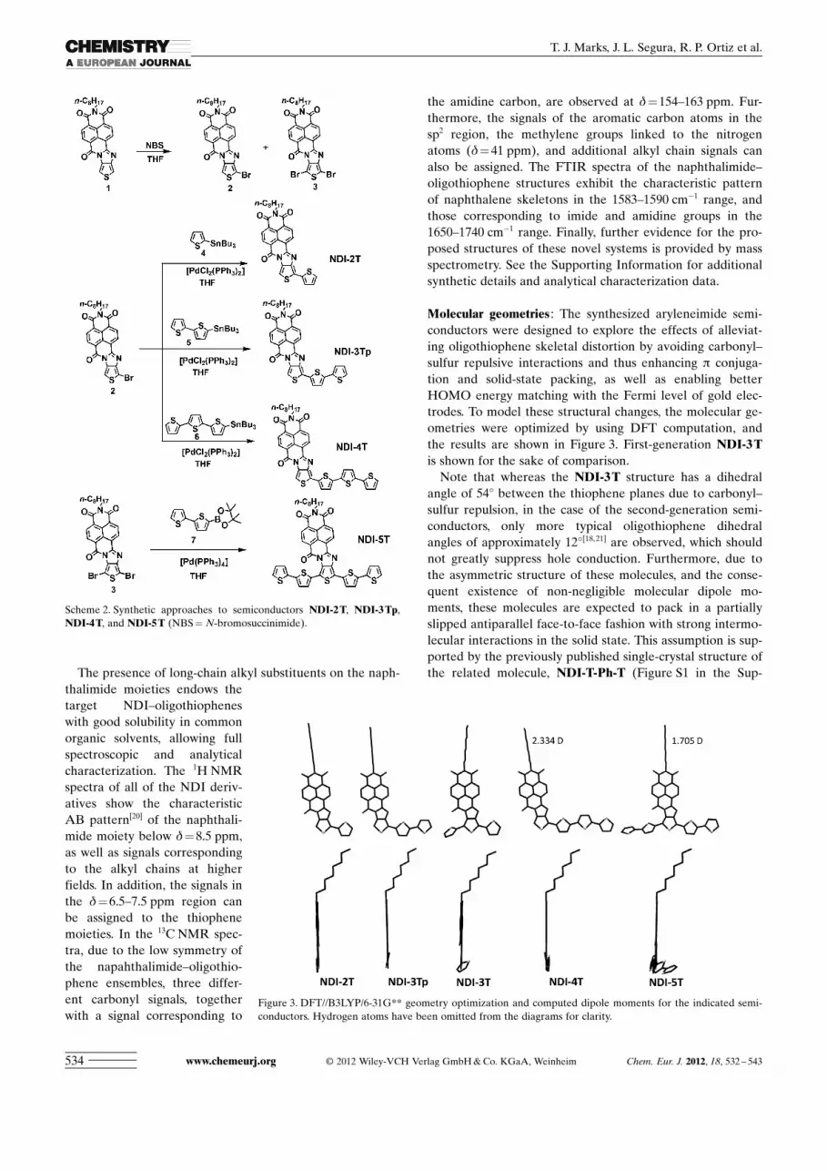
Synthetic strategy : The synthetic approaches to the targetmolecules NDI-2 T, NDI-3 Tp, NDI-4 T, and NDI-5 T areoutlined in Scheme 2, starting from the 2-octylbenzo-ACHTUNGTRENNUNG[lmn]thieno[3’,4’:4,5]imidazo ACHTUNGTRENNUNG[2,1-b]ACHTUNGTRENNUNG[3,8]phenanthroline-1,3,6-ACHTUNGTRENNUNG(2 H)-trione (1), previously synthesized in one of ourgroups.[18] Thus, bromination of 1 with N-bromosuccinimideaffords a mixture of the mono- (2) and dibromo derivatives(3), which can be separated by chromatography. The Stillecross-coupling reaction between 2 and the corresponding
stannanes 4, 5,[19] and 6[19] yieldsNDI-2 T, NDI-3 Tp, and NDI-4 T, respectively, in yields be-tween 57 and 65 %. In compari-son, the Suzuki cross-couplingreaction between dibromo de-rivative 3 and boronic ester 7affords NDI-5 T in a 46 % yield.As can be seen in Scheme 1,the use of monobromo deriva-tive 2 for the Stille coupling re-action in the synthesis of NDI-2 T, NDI-3 Tp, and NDI-4 T pre-vents skeletal distortions be-cause the non-bonded repulsionbetween the carbonyl group ofthe naphthalimide core and theoligothiophene sulfur atoms isabsent in these semiconductors.
Figure 1. Chemical structures of ambipolar arylene-based small moleculesand a related polymer.
Figure 2. First- and second-generation arylene–thiophene semiconductors.
Scheme 1. Sketch illustrating the sulfur–oxygen repulsive interactions infirst- and second-generation NDI/PDI–thiophene semiconductors.
Chem. Eur. J. 2012, 18, 532 – 543 � 2012 Wiley-VCH Verlag GmbH & Co. KGaA, Weinheim www.chemeurj.org 533
FULL PAPER
The presence of long-chain alkyl substituents on the naph-thalimide moieties endows thetarget NDI–oligothiopheneswith good solubility in commonorganic solvents, allowing fullspectroscopic and analyticalcharacterization. The 1H NMRspectra of all of the NDI deriv-atives show the characteristicAB pattern[20] of the naphthali-mide moiety below d= 8.5 ppm,as well as signals correspondingto the alkyl chains at higherfields. In addition, the signals inthe d=6.5–7.5 ppm region canbe assigned to the thiophenemoieties. In the 13C NMR spec-tra, due to the low symmetry ofthe napahthalimide–oligothio-phene ensembles, three differ-ent carbonyl signals, togetherwith a signal corresponding to
the amidine carbon, are observed at d=154–163 ppm. Fur-thermore, the signals of the aromatic carbon atoms in thesp2 region, the methylene groups linked to the nitrogenatoms (d= 41 ppm), and additional alkyl chain signals canalso be assigned. The FTIR spectra of the naphthalimide–oligothiophene structures exhibit the characteristic patternof naphthalene skeletons in the 1583–1590 cm�1 range, andthose corresponding to imide and amidine groups in the1650–1740 cm�1 range. Finally, further evidence for the pro-posed structures of these novel systems is provided by massspectrometry. See the Supporting Information for additionalsynthetic details and analytical characterization data.
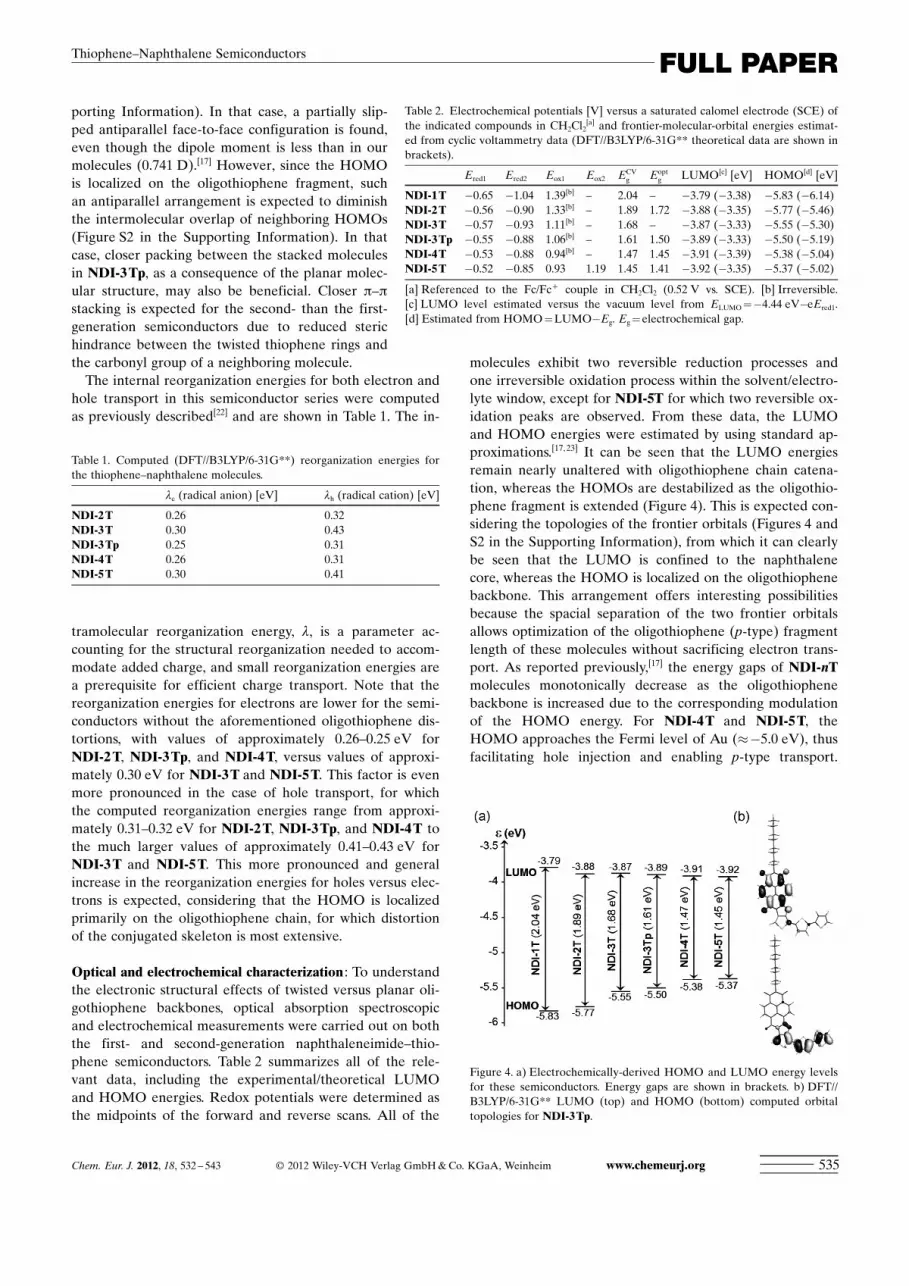
Molecular geometries : The synthesized aryleneimide semi-conductors were designed to explore the effects of alleviat-ing oligothiophene skeletal distortion by avoiding carbonyl–sulfur repulsive interactions and thus enhancing p conjuga-tion and solid-state packing, as well as enabling betterHOMO energy matching with the Fermi level of gold elec-trodes. To model these structural changes, the molecular ge-ometries were optimized by using DFT computation, andthe results are shown in Figure 3. First-generation NDI-3 Tis shown for the sake of comparison.
Note that whereas the NDI-3T structure has a dihedralangle of 548 between the thiophene planes due to carbonyl–sulfur repulsion, in the case of the second-generation semi-conductors, only more typical oligothiophene dihedralangles of approximately 128[18,21] are observed, which shouldnot greatly suppress hole conduction. Furthermore, due tothe asymmetric structure of these molecules, and the conse-quent existence of non-negligible molecular dipole mo-ments, these molecules are expected to pack in a partiallyslipped antiparallel face-to-face fashion with strong intermo-lecular interactions in the solid state. This assumption is sup-ported by the previously published single-crystal structure ofthe related molecule, NDI-T-Ph-T (Figure S1 in the Sup-
Scheme 2. Synthetic approaches to semiconductors NDI-2 T, NDI-3 Tp,NDI-4 T, and NDI-5 T (NBS = N-bromosuccinimide).
Figure 3. DFT//B3LYP/6-31G** geometry optimization and computed dipole moments for the indicated semi-conductors. Hydrogen atoms have been omitted from the diagrams for clarity.
www.chemeurj.org � 2012 Wiley-VCH Verlag GmbH & Co. KGaA, Weinheim Chem. Eur. J. 2012, 18, 532 – 543534
T. J. Marks, J. L. Segura, R. P. Ortiz et al.
porting Information). In that case, a partially slip-ped antiparallel face-to-face configuration is found,even though the dipole moment is less than in ourmolecules (0.741 D).[17] However, since the HOMOis localized on the oligothiophene fragment, suchan antiparallel arrangement is expected to diminishthe intermolecular overlap of neighboring HOMOs(Figure S2 in the Supporting Information). In thatcase, closer packing between the stacked moleculesin NDI-3 Tp, as a consequence of the planar molec-ular structure, may also be beneficial. Closer p–p
stacking is expected for the second- than the first-generation semiconductors due to reduced sterichindrance between the twisted thiophene rings andthe carbonyl group of a neighboring molecule.
The internal reorganization energies for both electron andhole transport in this semiconductor series were computedas previously described[22] and are shown in Table 1. The in-
tramolecular reorganization energy, l, is a parameter ac-counting for the structural reorganization needed to accom-modate added charge, and small reorganization energies area prerequisite for efficient charge transport. Note that thereorganization energies for electrons are lower for the semi-conductors without the aforementioned oligothiophene dis-tortions, with values of approximately 0.26–0.25 eV forNDI-2 T, NDI-3 Tp, and NDI-4 T, versus values of approxi-mately 0.30 eV for NDI-3T and NDI-5 T. This factor is evenmore pronounced in the case of hole transport, for whichthe computed reorganization energies range from approxi-mately 0.31–0.32 eV for NDI-2 T, NDI-3 Tp, and NDI-4 T tothe much larger values of approximately 0.41–0.43 eV forNDI-3 T and NDI-5 T. This more pronounced and generalincrease in the reorganization energies for holes versus elec-trons is expected, considering that the HOMO is localizedprimarily on the oligothiophene chain, for which distortionof the conjugated skeleton is most extensive.
Optical and electrochemical characterization : To understandthe electronic structural effects of twisted versus planar oli-gothiophene backbones, optical absorption spectroscopicand electrochemical measurements were carried out on boththe first- and second-generation naphthaleneimide–thio-phene semiconductors. Table 2 summarizes all of the rele-vant data, including the experimental/theoretical LUMOand HOMO energies. Redox potentials were determined asthe midpoints of the forward and reverse scans. All of the
molecules exhibit two reversible reduction processes andone irreversible oxidation process within the solvent/electro-lyte window, except for NDI-5T for which two reversible ox-idation peaks are observed. From these data, the LUMOand HOMO energies were estimated by using standard ap-proximations.[17, 23] It can be seen that the LUMO energiesremain nearly unaltered with oligothiophene chain catena-tion, whereas the HOMOs are destabilized as the oligothio-phene fragment is extended (Figure 4). This is expected con-sidering the topologies of the frontier orbitals (Figures 4 andS2 in the Supporting Information), from which it can clearlybe seen that the LUMO is confined to the naphthalenecore, whereas the HOMO is localized on the oligothiophenebackbone. This arrangement offers interesting possibilitiesbecause the spacial separation of the two frontier orbitalsallows optimization of the oligothiophene (p-type) fragmentlength of these molecules without sacrificing electron trans-port. As reported previously,[17] the energy gaps of NDI-nTmolecules monotonically decrease as the oligothiophenebackbone is increased due to the corresponding modulationof the HOMO energy. For NDI-4 T and NDI-5 T, theHOMO approaches the Fermi level of Au (��5.0 eV), thusfacilitating hole injection and enabling p-type transport.
Table 1. Computed (DFT//B3LYP/6-31G**) reorganization energies forthe thiophene–naphthalene molecules.
le (radical anion) [eV] lh (radical cation) [eV]
NDI-2 T 0.26 0.32NDI-3 T 0.30 0.43NDI-3 Tp 0.25 0.31NDI-4 T 0.26 0.31NDI-5 T 0.30 0.41
Table 2. Electrochemical potentials [V] versus a saturated calomel electrode (SCE) ofthe indicated compounds in CH2Cl2
[a] and frontier-molecular-orbital energies estimat-ed from cyclic voltammetry data (DFT//B3LYP/6-31G** theoretical data are shown inbrackets).
Ered1 Ered2 Eox1 Eox2 ECVg Eopt
g LUMO[c] [eV] HOMO[d] [eV]
NDI-1 T �0.65 �1.04 1.39[b] – 2.04 – �3.79 (�3.38) �5.83 (�6.14)NDI-2 T �0.56 �0.90 1.33[b] – 1.89 1.72 �3.88 (�3.35) �5.77 (�5.46)NDI-3 T �0.57 �0.93 1.11[b] – 1.68 – �3.87 (�3.33) �5.55 (�5.30)NDI-3 Tp �0.55 �0.88 1.06[b] – 1.61 1.50 �3.89 (�3.33) �5.50 (�5.19)NDI-4 T �0.53 �0.88 0.94[b] – 1.47 1.45 �3.91 (�3.39) �5.38 (�5.04)NDI-5 T �0.52 �0.85 0.93 1.19 1.45 1.41 �3.92 (�3.35) �5.37 (�5.02)
[a] Referenced to the Fc/Fc+ couple in CH2Cl2 (0.52 V vs. SCE). [b] Irreversible.[c] LUMO level estimated versus the vacuum level from ELUMO =�4.44 eV�eEred1.[d] Estimated from HOMO =LUMO�Eg. Eg = electrochemical gap.
Figure 4. a) Electrochemically-derived HOMO and LUMO energy levelsfor these semiconductors. Energy gaps are shown in brackets. b) DFT//B3LYP/6-31G** LUMO (top) and HOMO (bottom) computed orbitaltopologies for NDI-3 Tp.
Chem. Eur. J. 2012, 18, 532 – 543 � 2012 Wiley-VCH Verlag GmbH & Co. KGaA, Weinheim www.chemeurj.org 535
FULL PAPERThiophene–Naphthalene Semiconductors

Since the LUMO energies of the NDI-nT series remain ba-sically unaltered from those of the first-generation arylenea-midine imide-fused thiophene semiconductors (which are n-type semiconductors), ambipolar behavior might be expect-ed for them because their HOMO energies approach�5.0 eV.
Note also that the destabilization of the NDI-3 TpHOMO compared with NDI-3 T clearly reveals the disrup-tion of the conjugation in the latter due to the thiophenesulfur atom···carbonyl oxygen atom non-bonded repulsion.These steric effects were deliberately avoided in NDI-3 Tpand the other second-generation NDI-nT compounds. Thus,by using this design strategy, the NDI-3 Tp band gap is com-pressed by approximately 0.1 eV and the HOMO energyrises from �5.55 to �5.50 eV. This energy level readjust-ment, in conjunction with other factors, is likely the originof the ambipolar semiconduction, as argued in the followingsections.
As expected, the HOMO destabilization (�5.38 eV) isgreater in NDI-4T. Finally, for the sake of comparison, theelectrochemical results for NDI-5 T are also shown inTable 2. This semiconductor is particularly interesting be-cause it combines the planar oligothiophene fragment ofNDI-3 Tp with the skeletal twisting of NDI-3 T, translatinginto a band gap and HOMO/LUMO energies comparable tothose of NDI-4 T. These results are in good agreement withthe DFT calculations, in which identical energetic trends arefound (Figure S3 in the Supporting Information).
Optical absorption spectra of these semiconductors wererecorded in dichloromethane and the data are shown in Fig-ure S4 and Table S1 in the Supporting Information. Fromthese data, the optical band gaps were estimated from theonset of the lowest-energy absorptions. These values are ingood agreement with the electrochemically derived bandgaps. For all of these compounds, the broad absorption atwavelengths greater than 550 nm is assigned to an intramo-lecular charge-transfer excitation (ICT). This is theoreticallyconfirmed and can be described as a one-electron HOMO–LUMO excitation, consisting of the displacement of theelectron density from the HOMO, primarily localized on theoligothiophene fragment, to the LUMO, localized on thenaphthalene unit.
Thin film X-ray diffraction : Thin films of the present semi-conductors were grown either by vacuum sublimation or bydrop-casting onto OTS-functionalized, HMDS-functional-ized, or bare Si/SiO2 substrates, and their microstructuresanalyzed by wide-angle X-ray diffraction (WAXRD). Theseexperiments quantify out-of-plane d spacings, allowing esti-mation of the molecular orientation with respect to the gateinsulator surface for top-contact devices. The optimal micro-structural scenario for these semiconductor films is one inwhich the cofacial p-conjugated molecular planes arealigned perpendicular to the dielectric substrate surface, al-lowing more efficient charge transport between the sourceand drain electrodes.[24]
Figure 5 shows WAXRD data for NDI-3 Tp films growneither by sublimation or by solution-casting on HMDS-treat-ed substrates. It is clear that thin-film crystallinity is much
more pronounced for the sublimed films although all filmsare significantly textured. For all films, the most intensefamily of Bragg reflections is observed at similar 2q values(�3.08–3.178), with the occurrence of Bragg reflections upto the fifth order for vapor-deposited films and the fourthorder for drop-cast films, which is indicative of high crystal-linity. A further indication of the high semiconductor thin-film crystalline quality and long-range order is the appear-ance of Laue oscillations around the first-order Bragg dif-
Figure 5. q/2q X-ray diffraction scans of a) vapor-deposited and b) solu-tion-processed NDI-3 Tp thin films grown on HMDS-treated Si/SiO2 andannealed at the indicated temperatures.
www.chemeurj.org � 2012 Wiley-VCH Verlag GmbH & Co. KGaA, Weinheim Chem. Eur. J. 2012, 18, 532 – 543536
T. J. Marks, J. L. Segura, R. P. Ortiz et al.

fraction peaks of the vapor-deposited films, with these fea-tures most pronounced for films deposited at room tempera-ture.[24c]
Table 3 summarizes the d-spacing values derived for thedifferent NDI-3Tp films. Although assuming a parallel slip-ped configuration of the molecules affords larger HOMO–
HOMO overlap, such structures seem unlikely in view ofthe antiparallel packing of the related molecule NDI-T-Ph-T in the diffraction-determined single-crystal structure (Fig-ure S1 in the Supporting Information) and the computednon-negligible molecular dipole moments. For that reason,and because of the significant dipole moments of theseasymmetric molecules (computed to be 1.66–2.33 Debye),we assume that they are packed with pairwise intermolecu-lar interactions[17] orienting the naphthalene–diimide coresin opposite directions, as in the case of NDI-T-Ph-T (Fig-ure S1 in the Supporting Information). To simplify the dataanalysis, completely antiparallel face-to-face packing is con-sidered here, with the long axes of the pairs estimated to beapproximately 32.43 �; a possible partially slipped configu-ration is taken into account below. By using this approachand excluding alkyl group interdigitation, the molecular tiltangles with respect to the substrate surface normal can beestimated. This approximation provides an idea of the differ-ent microstructures and phases that exist within the films.The estimated molecular-tilt angles for NDI-3 Tp films de-posited under different conditions are quite similar, with dif-ferences of less than 28. Drop-cast films have slightly smallertilt angles than those of vapor-deposited films, which is usu-ally more favorable for charge hopping between source anddrain electrodes. Nevertheless, it should be noted that thetilt-angle estimation assumes identical alkyl chain interdigi-tation and packing motif for neighboring molecules in all ofthe samples. However, the small differences in d spacings
can also be explained by assuming approximately the sametilt angle along with alkyl group interdigitation. Note thatalthough the differences in d spacing are small, they are wellwithin the experimental uncertainty because the diffractiondata were all calibrated in situ with the Si substrate 004 re-flection. In that case, slightly different stacking motifs be-tween neighboring molecules are not unexpected in the caseof different d spacings (see Figure 6). A greater d spacing
for the solution-processed films would correlate with a moreslipped configuration. Considering that the two moleculesare packed in opposite directions, this would result in great-er intermolecular HOMO–HOMO overlap, as shown sche-matically in Figure 6.
Figure 7 shows the XRD diffraction patterns for vapor-de-posited NDI-4 T films grown under various conditions. It isclear that films deposited at room temperature only exhibita single phase with second-order reflections, whereas thosedeposited at 110 8C show dramatically enhanced crystallinity,with reflections up to the ninth order. NDI-4 T XRD dataare summarized in Table 3; tilt angles are estimated by usingthe same approximation as for NDI-3 Tp (see above).
Interestingly, all NDI-5 T films, deposited either by vapor-deposition or solution-casting, are amorphous. This can beascribed to poorly ordered packing due to the lost planarityof the oligothiophene skeleton in NDI-5 T, reflecting stericrepulsion with the adjacent carbonyl group. The same ab-sence of diffraction peaks was previously observed for NDI-3 T films for which similar skeletal distortions were found.[17]
In contrast, NDI-2 T films exhibit up to fourth-order sharpreflections for films vapor-deposited at 110 8C, with substan-
Table 3. Film X-ray diffraction data, d spacings, and estimated molecu-lar-tilt angles with respect to the surface normal for NDI-3 Tp and NDI-4T films deposited under different conditions.
Deposition conditions d spac-ing
Estimated
Method[a] Substrate[b] T[c]
[8C][�] tilt angle
[8]
Subl H 110 27.87 30.8Subl H 25 27.96 30.4Sol H 60 28.41 28.8Sol H 90 28.32 29.2Sol H 100 28.69 27.8Sol H 140 28.23 29.5Sol H as spun 28.23 29.5Subl H 110 28.32 29.2Subl S 110 28.23 29.5Subl H 25 28.23 29.5Subl S 25 28.32 29.2
[a] Subl=Sublimed films and Sol=Solution-processed films. [b] S=BareSi/SiO2 substrates and H =HMDS-functionalized substrates. [c] Deposi-tion or annealing temperature.
Figure 6. Sketch indicating two possible slipped configurations for NDI-3Tp films: a) the less slipped configuration, corresponding to a smaller dspacing; and b) the more slipped configuration, corresponding to a largerd spacing. The different HOMO and LUMO overlap for each case is alsoshown.
Chem. Eur. J. 2012, 18, 532 – 543 � 2012 Wiley-VCH Verlag GmbH & Co. KGaA, Weinheim www.chemeurj.org 537
FULL PAPERThiophene–Naphthalene Semiconductors

tially decreased crystallinity when growth is carried out atroom temperature (Figure S5 in the Supporting Informa-tion).
Semiconductor film morphology by AFM : In this section,we focus on the analysis of the surface morphology usingtapping mode AFM. The most important interface in afield-effect transistor is the dielectric-semiconductor inter-face where the charge transport occurs. Although AFM isunable to probe such buried interfaces, AFM images arewidely used to correlate film microstructure with chargetransport in the active region.[25] As shown in Figure 8, themorphologies of the vapor-deposited NDI-2 T films varysubstantially with the deposition temperature. Thus, filmsgrown on HMDS at room temperature are characterized byvery small rounded grains, whereas much larger rodlike
crystallites (�4–5 mm) are observed at higher growth tem-peratures. In the case of NDI-3 Tp films (Figure 9), AFM in-dicates small, well-interconnected grains for films grown on
HMDS and OTS-treated Si/SiO2 at room temperature.However, on HMDS these grains are rounded, whereas amore rodlike shape is observed for films grown on OTS. Athigher growth temperatures, we observe film dewetting andisland formation, reducing connectivity between the grains.This behavior is more pronounced for films deposited onHMDS-treated substrates in which large islands of dimen-sions greater than 1–2 mm are observed. NDI-4 T filmsbehave differently, with larger grains also seen for roomtemperature growth, and no dewetting detected even at hightemperatures (Figure 8) although the grain size increases.For solution-processed NDI-nT films, the effect of annealingtemperature on the film morphology was also investigated.Figure 9 shows AFM images of unannealed solution-pro-cessed NDI-3 Tp films, indicating small, rodlike structuredgrains. The grain dimensions increase substantially as the an-nealing temperature is increased. However, films annealedat very high temperatures are poorly connected. Finally, theAFM images of the NDI-5 T films support the formation ofamorphous films as observed by XRD above (Figure 8).
Semiconductor field-effect transistor characterization : Top-contact/bottom gate thin-film transistors were fabricatedwith films of the synthesized semiconductors to evaluatetheir charge-transport characteristics as a function of molec-ular architecture and film microstructure. Performance pa-rameters, which include field-effect mobility (m), thresholdvoltage (VT), and current on/off ratio (ION/IOFF), were ex-tracted from the I–V response plots in saturation regime byusing conventional transistor formalisms [Eq. (1)].
ðISDÞsat ¼�
W2L
�mCðVG�VTÞ2 ð1Þ
Figure 7. q/2q X-ray diffraction scans of vapor-deposited NDI-4 T thinfilms grown at the indicated temperatures on the SiO2 substrates func-tionalized as indicated.
Figure 8. AFM images of vapor-deposited NDI-2 T, NDI-4 T, and NDI-5T films grown at the temperatures indicated. Image sizes: 5� 5 mm;ev.= vapor-deposited film, sol. = spin-coated film.
Figure 9. AFM images of NDI-3 Tp films: a) vapor-deposited at the indi-cated temperatures, and b) solution-processed followed by annealing atthe indicated temperatures. Image sizes: 5� 5 mm.
www.chemeurj.org � 2012 Wiley-VCH Verlag GmbH & Co. KGaA, Weinheim Chem. Eur. J. 2012, 18, 532 – 543538
T. J. Marks, J. L. Segura, R. P. Ortiz et al.

Table 4 summarizes the field-effect transistor per-formance for films of all of the semiconductorsgrown by vapor deposition. Within this semiconduc-tor series, NDI-2 T exhibits the highest electron mo-bility, with a maximum value of 2.6 �10�2 cm2 V�1 s�1 for films grown at 110 8C. The FETperformance of NDI-2 T decreases by approximate-ly 10 fold for films grown at room temperature. Incontrast, NDI-3 T films are FET active only whendeposited at low temperatures and, interestingly,they are ambipolar when grown on OTS-treatedsubstrates, whereas only electron transport is ob-served for the films grown on HMDS-treated sub-strates. The parameters for films deposited on bareSi/SiO2 are not reported in Table 4 because they aresubstantially lower (�10 �), probably due to elec-tron trapping by dielectric surface SiOH groups.[5b]
Interestingly, all NDI-4T films are FET active andexhibit ambipolar behavior under the conditionsevaluated. However, far higher mobilities are ob-served for films deposited at 110 8C. NDI-5 T exhib-its by far the worst performance within the family,with mobilities no higher than 6.16 � 10�6 cm2 V�1 s�1, pre-sumably reflecting the oligothiophene skeletal distortionsdiscussed above.
Solution-processed NDI-3Tp and NDI-5 T FETs werefabricated by drop-casting, and the results are summarizedin Table 5. Due to the low solubility of NDI-4 T, solution-processed FETs of this semiconductor could not be fabricat-ed. The lower solubility of NDI-4 T compared with NDI-3 Tp can be explained due to higher p conjugation in theformer, which is known to decrease solubility. However, thesolubility of NDI-5 T increases due to its non-planar struc-ture, which diminishes conjugation and hinders tight packingwithin the crystal structure. Note that devices based on solu-tion-processed films exhibit ambipolar behavior under allmeasurement conditions. Thus, various film-annealing tem-peratures and solvent-evaporation rates were evaluated to
optimize performance. Unan-nealed NDI-3 Tp films exhibitambipolar behavior with maxi-mum electron and hole mobili-ties of 3.19 � 10�3 and 1.13 �10�3 cm2 V�1 s�1, respectively.Note that FET performance in-creases upon annealing thefilms at up to 90 8C. Thus, filmsannealed at 60 and 90 8C exhibitelectron and hole mobilities of1.07 � 10�2 and 5.69 �10�3 cm2 V�1 s�1, and 2.01 � 10�2
and 6.79 � 10�3 cm2 V�1 s�1, re-spectively. Figure 10 shows theoutput plots for electron andhole accumulation of an NDI-
3 Tp-based OFET annealed at 90 8C. The electron mobilitiesfor these solution-processed films are higher than thosemeasured for the corresponding vapor-deposited films(�10�3 cm2 V�1 s�1). Increasing the annealing temperaturesto >90 8C results in slightly lower field-effect mobilities al-though ambipolarity is still evident.
Discussion
Analysis of transistor electrical performance : In this section,the FET performance of the new thiophene–naphthalenesemiconductor series is analyzed in terms of molecularstructure and electronic properties, as well as thin-film mor-phology/microstructure characteristics. First, the NDI-2 T-based FETs exhibit electron mobility only. This result is not
Table 4. OFET electrical data for vapor-deposited films of the indicated semiconductors measured in vacuum.Average field-effect mobilities are shown (the highest mobility values are shown in brackets).
Substrate[a] T[b]
[8C]me (max)[cm2 V�1 s�1]
VT
[V]ION/IOFF mh (max)
[cm2 V�1 s�1]VT
[V]ION/IOFF
NDI-2 T H 110 1.41 � 10�2
(2.60�10�2)31 1 � 105
NDI-2 T H 25 2.11 � 10�3
(3.15�10�3)50 1 � 105
NDI-3 Tp H 25 1.27 � 10�3
(1.58�10�3)34 2 � 102
NDI-3 Tp O 25 1.83 � 10�3
(1.95�10�3)42 3 � 102 1.67 � 10�4
(1.67�10�4)�62 4� 102
NDI-4 T H 110 7.53 � 10�3
(9.19�10�3)41 1 � 102 1.13 � 10�3
(1.67�10�3)�51 10
NDI-4 T H 25 6.37 � 10�5
(6.70�10�5)28 3 � 102 4.79 � 10�5
(1.00�10�4)�59 1� 102
NDI-5 T H 110 3.21 � 10�6
(6.16�10�6)54 1 � 102
[a] H=HMDS-functionalized substrates and O=OTS-functionalized substrates. [b] Deposition temperature.
Table 5. OFET electrical data for solution-processed films of the indicated semicon-ductors annealed at the temperatures indicated and measured in vacuum. Averagefield-effect mobilities are shown (the highest mobility values are shown in brackets).
T[8C]
me (max)[cm2 V�1 s�1]
VT
[V]ION/IOFF mh (max)
[cm2 V�1 s�1]VT
[V]ION/IOFF
NDI-3 Tp as spun 2.44 � 10�3
(3.19�10�3)37 1 � 102 6.35 � 10�4
(1.13�10�3)�57 20
NDI-3 Tp 60 9.00 � 10�3
(1.07�10�2)33 4 � 102 2.95 � 10�3
(5.69�10�3)�64 40
NDI-3 Tp 90 1.10 � 10�2
(2.01�10�2)43 1 � 102 2.48 � 10�3
(6.79�10�3)�68 30
NDI-3 Tp 100 4.67 � 10�3
(5.21�10�3)39 4 � 102 8.46 � 10�4
(1.55�10�3)�64 10
NDI-3 Tp 120 3.07 � 10�3
(4.59�10�3)25 1 � 102 1.09 � 10�3
(2.30�10�3)�57 20
NDI-3 Tp 140 2.20 � 10�3
(2.94�10�3)20 5 � 102 6.10 � 10�4
(1.32�10�3)�61 50
NDI-3 Tp 180 2.63 � 10�3
(3.25�10�3)22 80 8.52 � 10�4
(1.29�10�3)�45 20
NDI-5 T 90 7.27 � 10�6
(8.52�10�6)5 10 1.40 � 10�5
(1.77�10�5)11 10
NDI-5 T 150 5.63 � 10�5
(1.02�10�4)27 5 � 103
Chem. Eur. J. 2012, 18, 532 – 543 � 2012 Wiley-VCH Verlag GmbH & Co. KGaA, Weinheim www.chemeurj.org 539
FULL PAPERThiophene–Naphthalene Semiconductors

surprising considering that although the LUMO energiesremain invariant within this new family of semiconductors,the NDI-2 T HOMO energy (�5.77 eV) is close to that ofNDI-1 T (�5.83 eV). Furthermore, the HOMO is confinedto the small bithiophene fragment, and this fragment is theonly molecular characteristic likely to stabilize hole carriers.Note that FET activity has not been reported to date forany bithiophene derivative. In contrast, the LUMO orbitalis localized on the naphthalene core, with a low energy of�3.87 eV, enabling facile electron transport. Indeed, NDI-2 T films exhibit a maximum electron mobility of 3.15 �10�3 cm2 V�1 s�1 when grown at room temperature. However,the mobility increases to as high as 2.6 �10�2 cm2 V�1 s�1 fora higher growth temperature (110 8C). This mobility en-hancement is due to the greater crystallinity of NDI-2 Tfilms grown at 110 8C, as judged by both the aforementionedXRD and AFM data. Note that for high deposition temper-atures, the XRD data exhibit sharp Bragg reflections up tothe fourth order and the AFM images show the appearanceof large rodlike grains (�4–5 mm), which should be benefi-cial for charge transport.
In contrast to the above results, the ambipolarity of theplanar molecules NDI-3 Tp and NDI-4 T can be understoodin terms of their architecture and electronic structure. Thereare three main reasons underlying their ambipolar behaviorcompared with first-generation thiophene–naphthalene sem-iconductors: 1) more planar structures that allow closer p–p
stacking and enhance intramolecular p conjugation; 2) dis-placement of the HOMO energies due to the extended oli-gothiophene core, which approaches the Fermi level of theAu electrodes; and 3) decreased reorganization energies for
both holes and electrons with respect to their non-planar ho-mologues, which thus facilitates the charge transport pro-cesses. However, the above conditions are necessary but notsufficient since our results show that film processing dramat-ically affects FET transport. Those trends can be explainedin terms of semiconductor film morphology, crystallinity,and molecular packing motifs. Note that head-to-tail crystalpacking of these molecules may hinder HOMO overlap tosome extent, and thus proper molecular stacking is essentialin enabling ambipolarity.
For the case of NDI-3 Tp, only electron mobility is evidentfor deposition on HMDS-treated substrates, whereas ambi-polar behavior is observed for films deposited on OTS atroom temperature. This different behavior can be ascribedto differing film morphologies, as shown in Figure 9, inwhich small round grains grow on HMDS, whereas rodlikeones predominate on OTS-coated substrates. Higher growthtemperatures afford inactive FETs, probably due to isolatedisland formation and film dewetting. However, for both theHMDS and OTS cases, field-effect performance is quite low,with electron mobilities of approximately 10�3 and hole mo-bilities of approximately 10�4 cm2 V�1 s�1 (see Table 4). Nev-ertheless, these parameters are substantially greater thanthose reported previously for the non-planar NDI-3 T (me =
3.5 � 10�4 cm2 V�1 s�1). This result is consistent with the great-er crystallinity and superior intermolecular orbital overlapin the planar semiconductors.
In contrast to these results, when NDI-3 Tp films are de-posited by drop-casting on HMDS-coated substrates andthen the films annealed at various temperatures, all of thesamples exhibit enhanced performance and ambipolar char-acteristics. The best result is found for samples annealed at90 8C, with maximum mobilities of 2.01 �10�2 and 6.79 �10�3 cm2 V�1 s�1 for electrons and holes, respectively, closelyfollowed by films annealed at 60 8C. Higher annealing tem-peratures result in decreased mobilities. This result is ingood agreement with the XRD data (Figure 5), in which thehighest crystallinity is found for annealing temperatures be-tween 60 8C and 100 8C, and lower crystallinity is found forunannealed or high-temperature annealed samples. Notethat NDI-3 Tp films annealed at 90 8C and 100 8C exhibithigher film XRD intensities and diffraction peaks up to thefourth order. Furthermore, AFM images indicate that whenannealing temperatures are increased, the grain sizes in-crease, however, they lose connectivity at very high anneal-ing temperatures (see Figure 9), which likely compromiseselectrical performance. Interestingly, the AFM images of so-lution-processed NDI-3 Tp films show rodlike structures, asobserved previously in sublimed films on OTS-coated sub-strates. However, the grain sizes of solution-processed filmsare much larger, which translates into higher mobilities. Thisobservation is intriguing because the films are deposited byrapid solvent evaporation, and thus smaller grain sizes mightbe expected. Another fact that should be taken into accountis that to aid solution spreading on the hydrophobic sub-strate, the tip of the pipette was used while the solvent wasevaporating, which could induce a different growth mor-
Figure 10. Output plot data for solution-processed NDI-3 Tp FETs an-nealed at 90 8C. a) electron transport characteristics, and b) hole transportcharacteristics. VG varies from �20 to 100 V (20 V steps) and from 20 to�100 V (�20 V steps), respectively.
www.chemeurj.org � 2012 Wiley-VCH Verlag GmbH & Co. KGaA, Weinheim Chem. Eur. J. 2012, 18, 532 – 543540
T. J. Marks, J. L. Segura, R. P. Ortiz et al.

phology compared to vapor phase growth on HMDS. Notealso that the different electrical performance of sublimed(n-type) versus solution-processed films (ambipolar) may bedue to differences in film morphologies/crystallinities. Infact, slightly different d spacings are found for solution-pro-cessed NDI-3 Tp films, which may allow slightly greateroverlap between the HOMOs of neighboring molecules.Furthermore, AFM images indicate larger rodlike grainsversus small rounded ones for vapor-deposited films onHMDS.
Regarding NDI-4 T films and devices, due to solubilitylimitations, only vapor-deposited samples were analyzed.Ambipolar behavior is observed for all of the films grown.However, lower performance (�10�4–10�5 cm2 V�1 s�1) isfound for films deposited at room temperature, which canbe ascribed to the observed film crystallinity and morpholo-gy. Note that the films grown at 25 8C show decreased crys-tallinity with only second-order diffraction peaks versus theninth-order diffraction peaks shown for films grown at110 8C. Furthermore, Figure 8 shows that films grown atroom temperature exhibit small, rounded grains similar tothe ones seen for NDI-3 Tp deposited under similar condi-tions (Figure 9), and both film types afford low FET perfor-mance. In contrast, when the thin films are deposited onHMDS at 110 8C, larger and less well-defined roundedgrains are formed (Figure 8), and performance is increasedby two orders of magnitude, with the highest mobilitiesbeing 9.19 � 10�3 and 1.67 �10�3 cm2 V�1 s�1, for electrons andholes, respectively.
p-Conjugation versus crystallinity? The case of NDI-5 T: Todetermine whether the origin of the ambipolarity in theseplanar second-generation thiophene–naphthalene semicon-ductors is due to increased intramolecular conjugation and/or to increased intermolecular HOMO–HOMO overlap dueto denser crystal packing, we synthesized the semiconductorNDI-5 T. This molecule combines the same skeletal distor-tions found in NDI-3 T, which hinders close crystal packing,but exhibits increased p conjugation, as found in NDI-3 Tp.The degree of p conjugation is estimated by calculating thebond length alternation parameter (BLA), which is the dif-ference between the average lengths of single and doubleconjugated C�C bonds of the oligothiophene skeleton, andis related to the extent of molecular aromatization/quinoidi-zation.[26] Thus, a lower BLA parameter indicates greaterquinoidization and hence, a more conjugated structure. Toestimate the extent of the p conjugation, molecular optimi-zations of NDI-3 T, NDI-3 Tp, and NDI-5 T were carried outby using DFT techniques, and the BLA parameters were es-timated by using the optimized bond lengths (Figure S6 inthe Supporting Information). Considering that every mole-cule under discussion here is connected similarly to an ary-lene fragment, it is reasonable to assume that the BLA pa-rameter of the oligothiophene fragment should be sufficientto estimate the p conjugation. The BLA parameter of theterthiophene skeleton in NDI-3 T is 0.056 �, and decreasesto 0.052 � for NDI-3 Tp, in good agreement with the expect-
ed increased conjugation due to the molecular planarity.Furthermore, the BLA value for the oligothiophene frag-ment in NDI-3 Tp corresponds with that of NDI-5 T, indicat-ing a similar degree of p-conjugation.
FETs fabricated through NDI-5 T vapor deposition areexclusively n-type devices and exhibit very low mobilities ofapproximately 3.21 �10�6 cm2 V�1 s�1. However, solution-pro-cessed films of NDI-5 T, annealed at 90 8C, exhibit ambipolartransport characterized by low, but balanced, hole and elec-tron mobilities of approximately 10�5 cm2 V�1 s�1. These re-sults argue that skeletal distortion is not the principal effecthindering hole transport, although it certainly decreasesfield-effect mobility due to the decreased film order (as seenin the XRD data). Rather, we believe that the absence ofambipolarity in NDI-3 T is due principally to decreased p
conjugation, which destabilizes the HOMO, even if filmcrystallinity and morphology may also play a role.
Conclusion
We have synthesized and characterized a new planar thio-phene–naphthalene semiconductor series for n-type and am-bipolar OFETs, and compared the structural and electricalproperties with a homologous series of molecularly twistedsemiconductors. Specifically, OFETs fabricated from solu-tion-processed NDI-3 Tp films on HMDS-treated substrates,annealed at 90 8C exhibit the best performance, with maxi-mum mobilities of 2.01 �10�2 and 6.79 � 10�3 cm2 V�1 s�1 forelectrons and holes, respectively. These mobilities are sub-stantially larger than those previously reported for the geo-metrically twisted counterpart, NDI-3 T, which exhibits onlyelectron mobility (3.5 �10�4 cm2 V�1 s�1). The presence ofambipolar transport in these planar molecules can be under-stood on the basis of three interrelated properties that formthe basis for ambipolar materials design: 1) the absence ofskeletal distortions allows closer intermolecular p–p stack-ing and enhanced intramolecular p conjugation; 2) increasedp conjugation raises the HOMO energy, which approachesthe Fermi level of the Au electrodes; and 3) more planarstructures translate into lower Marcus reorganization ener-gies. Furthermore, by comparing the structural and FETproperties of NDI-3 T, NDI-3 Tp, and NDI-5 T we have dem-onstrated that the absence of ambipolarity in NDI-3 T ismainly due to the disrupted p conjugation, although thelower crystallinity induced by the skeletal distortions de-creases carrier mobility.
Acknowledgements
We thank AFOSR (FA9550-08-01-0331) and the NSF-MRSEC programthrough the Northwestern Materials Research Center (DMR-0520513)for support of this research at Northwestern University. We also thankComunidad Aut�noma de Madrid (project S2009/MAT-1467, the UCM-BSCH joint project (GR35/10 A-910759), and the MCyT of Spain(CTQ2010-14982) for financial support. R.P.O. acknowledges fundingfrom the European Community�s Seventh Framework Programme
Chem. Eur. J. 2012, 18, 532 – 543 � 2012 Wiley-VCH Verlag GmbH & Co. KGaA, Weinheim www.chemeurj.org 541
FULL PAPERThiophene–Naphthalene Semiconductors

through a Marie Curie International Outgoing Fellowship (Grant Agree-ment 234808).
[1] a) Z. Y. Chen, H. Lemke, S. Albert-Seifried, M. Caironi, M. M. Niel-sen, M. Heeney, W. M. Zhang, I. McCulloch, H. Sirringhaus, Adv.Mater. 2010, 22, 2371 – 2375; b) H. Jiang, Macromol. RapidCommun. 2010, 31, 2007 –2034; c) Y. Y. Liu, C. L. Song, W. J. Zeng,K. G. Zhou, Z. F. Shi, C. B. Ma, F. Yang, H. L. Zhang, X. Gong, J.Am. Chem. Soc. 2010, 132, 16349 –16351; d) T. T. Steckler, X.Zhang, J. Hwang, R. Honeyager, S. Ohira, X. H. Zhang, A. Grant,S. Ellinger, S. A. Odom, D. Sweat, D. B. Tanner, A. G. Rinzler, S.Barlow, J. L. Bredas, B. Kippelen, S. R. Marder, J. R. Reynolds, J.Am. Chem. Soc. 2009, 131, 2824 –2826; e) H. Usta, A. Facchetti, T. J.Marks, J. Am. Chem. Soc. 2008, 130, 8580 –8581; f) S. Handa, E.Miyazaki, K. Takimiya, Chem. Commun. 2009, 3919 – 3921; g) A. P.Kulkarni, Y. Zhu, A. Babel, P. T. Wu, S. A. Jenekhe, Chem. Mater.2008, 20, 4212 – 4223; h) M. L. Tang, A. D. Reichardt, N. Miyaki,R. M. Stoltenberg, Z. Bao, J. Am. Chem. Soc. 2008, 130, 6064 –6065.
[2] a) B. Yoo, T. Jung, D. Basu, A. Dodabalapur, B. A. Jones, A. Fac-chetti, M. R. Wasielewski, T. J. Marks, Appl. Phys. Lett. 2006, 88,082104; b) J. Zaumseil, H. Sirringhaus, Chem. Rev. 2007, 107, 1296 –1323; c) H. Yan, Z. H. Chen, Y. Zheng, C. Newman, J. R. Quinn, F.Dotz, M. Kastler, A. Facchetti, Nature 2009, 457, 679 – 686; d) J. C.Ribierre, S. Watanabe, M. Matsumoto, T. Muto, A. Nakao, T.Aoyama, Adv. Mater. 2010, 22, 4044 –4048; e) F. S. Kim, X. G. Guo,M. D. Watson, S. A. Jenekhe, Adv. Mater. 2010, 22, 478 –482; f) E. J.Meijer, D. M. De Leeuw, S. Setayesh, E. Van Veenendaal, B. H.Huisman, P. W. M. Blom, J. C. Hummelen, U. Scherf, T. M. Klap-wijk, Nature Mater. 2003, 2, 678 – 682; g) H. Sirringhaus, T. Kawase,R. H. Friend, T. Shimoda, M. Inbasekaran, W. Wu, E. P. Woo, Sci-ence 2000, 290, 2123 –2126; h) H. Klauk, U. Zschieschang, J. Pflaum,M. Halik, Nature 2007, 445, 745 –748; i) T. H. Jung, B. Yoo, L. Wang,A. Dodabalapur, B. A. Jones, A. Facchetti, M. R. Wasielewski, T. J.Marks, Appl. Phys. Lett. 2006, 88, 183102; j) B. Yoo, B. A. Jones, D.Basu, D. Fine, T. Jung, S. Mohapatra, A. Facchetti, K. Dimmler,M. R. Wasielewski, T. J. Marks, A. Dodabalapur, Adv. Mater. 2007,19, 4028 – 4032; k) X. Guo, R. P. Ortiz, Y. Zheng, Y. Hu, Y.-Y. Noh,K.-J. Baeg, A. Facchetti, T. J. Marks, J. Am. Chem. Soc. 2011, 133,1405 – 1418.
[3] B. Crone, A. Dodabalapur, A. Gelperin, L. Torsi, H. E. Katz, A. J.Lovinger, Z. Bao, Appl. Phys. Lett. 2001, 78, 2229 –2231.
[4] a) F. Dinelli, R. Capelli, M. A. Loi, M. Murgia, M. Muccini, A. Fac-chetti, T. J. Marks, Adv. Mater. 2006, 18, 1416 –1420; b) R. Capelli, S.Toffanin, G. Generali, H. Usta, A. Facchetti, M. Muccini, Nat.Mater. 2010, 9, 496 –503; c) M. Muccini, Nat. Mater. 2006, 5, 605 –613.
[5] a) J. Cornil, J. L. Bredas, J. Zaumseil, H. Sirringhaus, Adv. Mater.2007, 19, 1791 – 1799; b) L. L. Chua, J. Zaumseil, J. F. Chang,E. C. W. Ou, P. K. H. Ho, H. Sirringhaus, R. H. Friend, Nature 2005,434, 194 –199.
[6] a) J. Zaumseil, R. H. Friend, H. Sirringhaus, Nature Mater. 2006, 5,69– 74; b) J. S. Swensen, C. Soci, A. J. Heeger, Appl. Phys. Lett.2005, 87, 253511.
[7] R. Ponce Ortiz, A. Facchetti, T. J. Marks, Chem. Rev. 2010, 110,205 – 239.
[8] a) M. Halik, H. Klauk, U. Zschieschang, G. Schmid, C. Dehm, M.Schutz, S. Maisch, F. Effenberger, M. Brunnbauer, F. Stellacci,Nature 2004, 431, 963 – 966; b) R. T. Weitz, U. Zschieschang, F. Ef-fenberger, H. Klauk, M. Burghard, K. Kern, Nano Lett. 2007, 7, 22 –27; c) U. Zschieschang, M. Halik, H. Klauk, Langmuir 2008, 24,1665 – 1669.
[9] a) S. A. DiBenedetto, A. Facchetti, M. A. Ratner, T. J. Marks, Adv.Mater. 2009, 21, 1407 – 1433; b) M. H. Yoon, A. Facchetti, T. J.Marks, Proc. Natl. Acad. Sci. U.S.A. 2005, 102, 4678 – 4682.
[10] T. Yamamoto, T. Yasuda, Y. Sakai, S. Aramaki, A. Ramaw, Macro-mol. Rapid Commun. 2005, 26, 1214 –1217.
[11] B. J. Jung, N. J. Tremblay, M.-L. Yeh, H. E. Katz, Chem. Mater. 2011,23, 568 –582.
[12] a) K. C. See, C. Landis, A. Sarjeant, H. E. Katz, Chem. Mater. 2008,20, 3609 –3616; b) R. J. Chesterfield, J. C. McKeen, C. R. Newman,P. C. Ewbank, D. A. da Silva, J. L. Bredas, L. L. Miller, K. R. Mann,C. D. Frisbie, J. Phys. Chem. B 2004, 108, 19281 –19292; c) R. J.Chesterfield, J. C. McKeen, C. R. Newman, C. D. Frisbie, P. C.Ewbank, K. R. Mann, L. L. Miller, J. Appl. Phys. 2004, 95, 6396 –6405; d) P. R. L. Malenfant, C. D. Dimitrakopoulos, J. D. Gelorme,L. L. Kosbar, T. O. Graham, A. Curioni, W. Andreoni, Appl. Phys.Lett. 2002, 80, 2517 –2519; e) S. Tatemichi, M. Ichikawa, T. Koyama,Y. Taniguchi, Appl. Phys. Lett. 2006, 89, 112108; f) D. Shukla, S. F.Nelson, D. C. Freeman, M. Rajeswaran, W. G. Ahearn, D. M.Meyer, J. T. Carey, Chem. Mater. 2008, 20, 7486 – 7491; g) X. W.Zhan, A. Facchetti, S. Barlow, T. J. Marks, M. A. Ratner, M. R. Wa-sielewski, S. R. Marder, Adv. Mater. 2011, 23, 268 –284.
[13] a) R. Schmidt, J. H. Oh, Y. S. Sun, M. Deppisch, A. M. Krause, K.Radacki, H. Braunschweig, M. Konemann, P. Erk, Z. A. Bao, F.Wurthner, J. Am. Chem. Soc. 2009, 131, 6215 –6228; b) R. Schmidt,M. M. Ling, J. H. Oh, M. Winkler, M. Konemann, Z. N. Bao, F.Wurthner, Adv. Mater. 2007, 19, 3692 – 3695; c) M. M. Ling, P. Erk,M. Gomez, M. Koenemann, J. Locklin, Z. N. Bao, Adv. Mater. 2007,19, 1123 –1127; d) H. Z. Chen, M. M. Ling, X. Mo, M. M. Shi, M.Wang, Z. Bao, Chem. Mater. 2007, 19, 816 –824; e) Y. Hosoi, D. Tsu-nami, I. Hisao, Y. Furukawa, Chem. Phys. Lett. 2007, 436, 139 –143;f) Y. Li, L. Tan, Z. H. Wang, H. L. Qian, Y. B. Shi, W. P. Hu, Org.Lett. 2008, 10, 529 –532; g) B. A. Jones, M. J. Ahrens, M. H. Yoon,A. Facchetti, T. J. Marks, M. R. Wasielewski, Angew. Chem. 2004,116, 6523 –6526; Angew. Chem. Int. Ed. 2004, 43, 6363 –6366;h) B. A. Jones, A. Facchetti, M. R. Wasielewski, T. J. Marks, J. Am.Chem. Soc. 2007, 129, 15259 –15278; i) B. A. Jones, A. Facchetti, T. J.Marks, M. R. Wasielewski, Chem. Mater. 2007, 19, 2703 –2705.
[14] H. N. Tsao, W. Pisula, Z. H. Liu, W. Osikowicz, W. R. Salaneck, K.M�llen, Adv. Mater. 2008, 20, 2715 –2719.
[15] C. A. Liu, Z. H. Liu, H. T. Lemke, H. N. Tsao, R. C. G. Naber, Y. Li,K. Banger, K. Mullen, M. M. Nielsen, H. Sirringhaus, Chem. Mater.2010, 22, 2120 –2124.
[16] H. Kr�ger, S. Janietz, D. Sainova, D. Dobreva, N. Koch, A. Vollmer,Adv. Funct. Mater. 2007, 17, 3715 –3723.
[17] R. Ponce Ortiz, H. Herrera, R. Blanco, H. Huang, A. Facchetti, T. J.Marks, Y. Zheng, J. L. Segura, J. Am. Chem. Soc. 2010, 132, 8440 –8452.
[18] S. R. Gonz�lez, J. Casado, J. T. L�pez Navarrete, R. L. Blanco, J. L.Segura, J. Phys. Chem. A 2008, 112, 6732 – 6740.
[19] A. Bilge, A. Zen, M. Forster, H. Li, F. Galbrecht, B. S. Nehls, T. Far-rell, D. Neher, U. Scherf, J. Mater. Chem. 2006, 16, 3177 –3182.
[20] a) P. Fellmann, C. Cordier, A. Gevertz, J. Chem. Educ. 2006, 83,432 – 435; b) L. C. Hoskins, J. Chem. Educ. 1991, 68, 83 –84.
[21] a) A. Facchetti, M.-H. Yoon, C. L. Stern, H. E. Katz, T. J. Marks,Angew. Chem. 2003, 115, 4030 –4033; b) A. Yassar, G. Horowitz, P.Valat, V. Wintgens, M. Hmyene, F. Deloffre, P. Srivastava, P. Lang,F. Garnier, J. Phys. Chem. 1995, 99, 9155 – 9159; c) S. Hotta, K. War-agai, Adv. Mater. 1993, 5, 896 – 908.
[22] M. Malagoli, J. L. Bredas, Chem. Phys. Lett. 2000, 327, 13– 17.[23] a) M. Dal Colle, C. Cova, G. Distefano, D. Jones, A. Modelli, N.
Comisso, J. Phys. Chem. A 1999, 103, 2828 – 2835; b) R. Ponce Ortiz,J. Casado, V. Hernandez, J. T. L�pez Navarrete, J. A. Letizia, M. A.Ratner, A. Facchetti, T. J. Marks, Chem. Eur. J. 2009, 15, 5023 –5039; c) M. H. Yoon, S. A. DiBenedetto, M. T. Russell, A. Facchetti,T. J. Marks, Chem. Mater. 2007, 19, 4864 –4881.
[24] a) G. Horowitz, J. Mater. Res. 2004, 19, 1946 – 1962; b) Y. M. Sun,Y. Q. Liu, D. B. Zhu, J. Mater. Chem. 2005, 15, 53–65; c) B. D. Culli-ty, S. R. Stock, Elements of X-Ray Diffraction, 3rd ed., PrenticeHall, Upper Saddle River, 2001.
[25] a) T. S. Huang, Y. K. Su, P. C. Wang, Appl. Phys. Lett. 2007, 91,092116; b) P. Kim, X. H. Zhang, B. Domercq, S. C. Jones, P. J.Hotchkiss, S. R. Marder, B. Kippelen, J. W. Perry, Appl. Phys. Lett.2008, 93, 013302; c) J. Lee, J. H. Kim, S. Im, J. Appl. Phys. 2004, 95,3733 – 3736; d) S. Y. Park, M. Park, H. H. Lee, Appl. Phys. Lett.2004, 85, 2283 –2285; e) S. Pyo, H. Son, K. Y. Choi, M. H. Yi, S. K.Hong, Appl. Phys. Lett. 2005, 86, 133508.
www.chemeurj.org � 2012 Wiley-VCH Verlag GmbH & Co. KGaA, Weinheim Chem. Eur. J. 2012, 18, 532 – 543542
T. J. Marks, J. L. Segura, R. P. Ortiz et al.

[26] a) C. Moreno Castro, M. C. R. Delgado, V. Hernandez, S. Hotta, J.Casado, J. T. L. Navarrete, J. Chem. Phys. 2002, 116, 10419 –10427;b) R. Ponce Ortiz, J. Casado, S. Rodriguez Gonzalez, V. Hernandez,J. T. Lopez Navarrete, P. M. Viruela, E. Orti, K. Takimiya, T.Otsubo, Chem. Eur. J. 2010, 16, 470 – 484; c) J. Casado, R. P. Ortiz,
M. C. R. Delgado, R. Azumi, R. T. Oakley, V. Hernandez, J. T. L.Navarrete, J. Phys. Chem. B 2005, 109, 10115 – 10125.
Received: June 6, 2011Published online: December 12, 2011
Chem. Eur. J. 2012, 18, 532 – 543 � 2012 Wiley-VCH Verlag GmbH & Co. KGaA, Weinheim www.chemeurj.org 543
FULL PAPERThiophene–Naphthalene Semiconductors


