Embed Size (px)
Citation preview
arX
iv:c
ond-
mat
/060
2282
v1 [
cond
-mat
.sof
t] 1
0 Fe
b 20
06APS/123-QED
Hyperfine interaction and magnetoresistance in organic semiconductors
Y. Sheng1, D. T. Nguyen1, G. Veeraraghavan2, O. Mermer1, M. Wohlgenannt1∗ and U. Scherf31Department of Physics and Astronomy and Optical Science and Technology Center,
University of Iowa, Iowa City, IA 52242-1479, USA2Department of Electrical and Computer Engineering and Optical Science and Technology Center,
University of Iowa, Iowa City, IA 52242-1595, USA and3Bergische Universitat Wuppertal, Fachbereich Chemie,
Makromolekulare Chemie, D-42097 Wuppertal, Germany
(Dated: February 6, 2008)
We explore the possibility that hyperfine interaction causes the recently discovered organic mag-netoresistance (OMAR) effect. Our study employs both experiment and theoretical modelling. Anexcitonic pair mechanism model based on hyperfine interaction, previously suggested by others toexplain magnetic field effects in organics, is examined. Whereas this model can explain a few keyaspects of the experimental data, we, however, uncover several fundamental contradictions as well.By varying the injection efficiency for minority carriers in the devices, we show experimentally thatOMAR is only weakly dependent on the ratio between excitons formed and carriers injected, likelyexcluding any excitonic effect as the origin of OMAR.
PACS numbers: 73.50.-h,73.50.Qt,
I. INTRODUCTION
Organic π-conjugated materials have been used tomanufacture devices such as organic light-emitting diodes(OLEDs) [1, 2], photovoltaic cells [3, 4, 5] and field-effecttransistors [6, 7, 8]. Recently there has been growing in-terest in spin [9, 10, 11, 12] and magnetic field effects(MFE) [13, 14, 15, 16, 17, 18, 19, 20, 21, 22, 23] inthese materials. Frankevich and coworkers [24, 25] andKalinowski and coworkers [22, 26] studied the effect ofsmall magnetic fields on excitonic processes that occur inOLEDs, such as photoconductivity, electroluminescence(EL) and exciton dissociation at the electrodes. Theyhave convincingly explained their findings using a modelwhere the applied magnetic field reduces the effect of thehyperfine interaction between electron/hole spin and thehydrogen nuclei in the organic molecules. We will referto this work as the excitonic pair mechanism model thatwill be treated in detail in section IVC.
We recently discovered [13] a large and intriguing mag-netoresistive effect in OLEDs, which we dubbed organicmagnetoresistance (OMAR). OMAR may find applica-tion in magnetic field sensors, e.g. in OLED interactivedisplays (patent pending, see demonstration video in Ref.[13]). In addition to its potential applications, OMARposes a significant scientific puzzle since it is, to the bestof our knowledge, the only known example of large roomtemperature magnetoresistance in non-magnetic materi-als with the exception of narrow-gap high-mobility ma-terials [27].
In the present work we examine whether the excitonicpair mechanism model [22, 24, 26] can explain OMAR.For this purpose we recast this model (see section IVC)
∗Electronic address: [email protected]
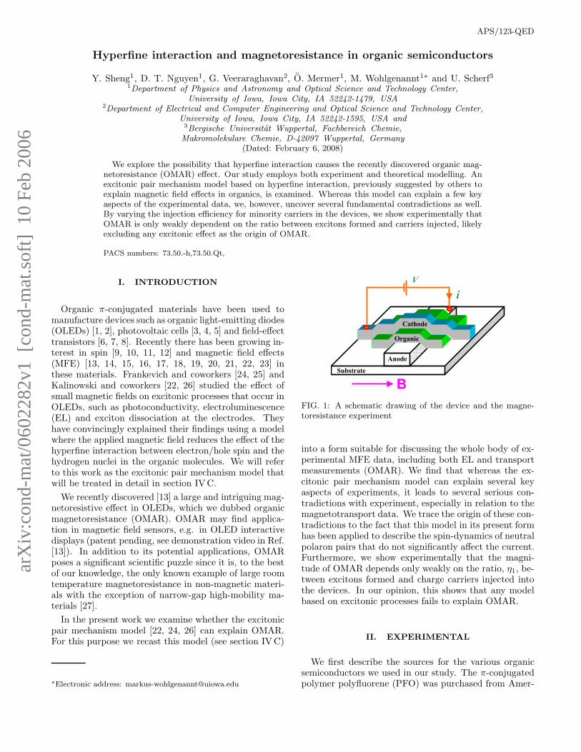
Substrate
B
Anode
Organic
Cathode
i
V
FIG. 1: A schematic drawing of the device and the magne-toresistance experiment
into a form suitable for discussing the whole body of ex-perimental MFE data, including both EL and transportmeasurements (OMAR). We find that whereas the ex-citonic pair mechanism model can explain several keyaspects of experiments, it leads to several serious con-tradictions with experiment, especially in relation to themagnetotransport data. We trace the origin of these con-tradictions to the fact that this model in its present formhas been applied to describe the spin-dynamics of neutralpolaron pairs that do not significantly affect the current.Furthermore, we show experimentally that the magni-tude of OMAR depends only weakly on the ratio, η1, be-tween excitons formed and charge carriers injected intothe devices. In our opinion, this shows that any modelbased on excitonic processes fails to explain OMAR.
II. EXPERIMENTAL
We first describe the sources for the various organicsemiconductors we used in our study. The π-conjugatedpolymer polyfluorene (PFO) was purchased from Amer-
2
ican Dye Source, inc. The methyl-substituted ladder-type poly(p-phenylene) (MeLPPP) polymer was synthe-sized as described elsewhere [28]. The π-conjugated smallmolecule Alq3 was purchased from H. W. Sands corpo-ration and was used as received.
The fabrication of the organic sandwich devices startedwith glass substrates coated with 40nm of indium-tin-oxide (ITO), purchased from Delta Technologies. Theconducting polymer Poly (3,4-ethylenedioxythiophene)-poly (styrenesulfonate) (PEDOT), purchased from H. C.Starck was spin coated at 2000 rpm on top of the ITOto provide an efficient hole injecting electrode. All othermanufacturing steps were carried out in a nitrogen glovebox. The active polymer film was spin coated onto thesubstrate from a chloroform solution. The small molec-ular film layers were made by thermal evaporation. Thecathode, either Ca (with an Al capping layer), Al, or Au,was then deposited by thermal (Ca) or electron beamevaporation (Al, Au) at a base pressure of ≈ 1 × 10⁻⁶
mbar on top of the organic thin films. The device areawas ≈ 1mm2 for all devices. The general device structureused for our measurements was metal/organic semicon-ductor/metal (see Fig. 1).
A schematic drawing of the device and the experimentare shown in Fig. 1. The samples were mounted on thecold finger of a closed-cycle helium cryostat located be-tween the poles of an electromagnet. The magnetocon-ductance ratio, ∆I/I, was determined by measuring thecurrent, I, at a constant applied voltage, V , for differentmagnetic fields, B. EL of the devices was measured witha photomultiplier tube that was shielded from the mag-netic field using high-saturation mu-shield foil. All thereported data are for room temperature.
III. EXPERIMENTAL RESULTS, PART I
A. Magnetic Field Effect on Current and
Electroluminescence
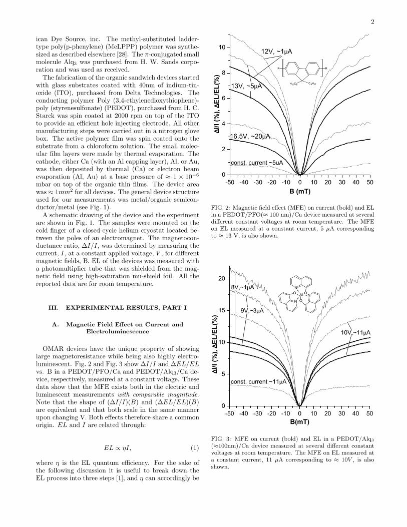
OMAR devices have the unique property of showinglarge magnetoresistance while being also highly electro-luminescent. Fig. 2 and Fig. 3 show ∆I/I and ∆EL/ELvs. B in a PEDOT/PFO/Ca and PEDOT/Alq3/Ca de-vice, respectively, measured at a constant voltage. Thesedata show that the MFE exists both in the electric andluminescent measurements with comparable magnitude.Note that the shape of (∆I/I)(B) and (∆EL/EL)(B)are equivalent and that both scale in the same mannerupon changing V. Both effects therefore share a commonorigin. EL and I are related through:
EL ∝ ηI, (1)
where η is the EL quantum efficiency. For the sake ofthe following discussion it is useful to break down theEL process into three steps [1], and η can accordingly be
-50 -40 -30 -20 -10 0 10 20 30 40 50
0
2
4
6
8
10
H17C8 C8H17
R R
13V, ~5µA
16.5V, ~20µA
∆∆ ∆∆I/I (%), ∆∆ ∆∆EL/EL(%)
B (mT)
const. current ~5uA
12V, ~1µA
FIG. 2: Magnetic field effect (MFE) on current (bold) and ELin a PEDOT/PFO(≈ 100 nm)/Ca device measured at severaldifferent constant voltages at room temperature. The MFEon EL measured at a constant current, 5 µA correspondingto ≈ 13 V, is also shown.
-50 -40 -30 -20 -10 0 10 20 30 40 50
0
5
10
15
20
∆∆ ∆∆I/I (%), ∆∆ ∆∆EL/EL(%)
N
ON
O
Al
N
O
10V,~11µA
9V,~3µA
B(mT)
8V,~1µA
const. current ~11µA
FIG. 3: MFE on current (bold) and EL in a PEDOT/Alq3
(≈100nm)/Ca device measured at several different constantvoltages at room temperature. The MFE on EL measured ata constant current, 11 µA corresponding to ≈ 10V , is alsoshown.
3
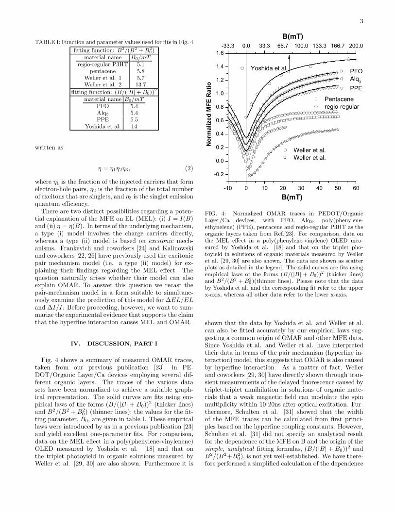
TABLE I: Function and parameter values used for fits in Fig. 4
fitting function: B2/(B2 + B2
0)material name B0/mT
regio-regular P3HT 5.1pentacene 5.8
Weller et al. 1 5.7Weller et al. 2 13.7
fitting function: (B/(|B| + B0))2
material name B0/mTPFO 5.4Alq3 5.4PPE 5.5
Yoshida et al. 14
written as
η = η1η2η3, (2)
where η1 is the fraction of the injected carriers that formelectron-hole pairs, η2 is the fraction of the total numberof excitons that are singlets, and η3 is the singlet emissionquantum efficiency.
There are two distinct possibilities regarding a poten-tial explanation of the MFE on EL (MEL): (i) I = I(B)and (ii) η = η(B). In terms of the underlying mechanism,a type (i) model involves the charge carriers directly,whereas a type (ii) model is based on excitonic mech-anisms. Frankevich and coworkers [24] and Kalinowskiand coworkers [22, 26] have previously used the excitonicpair mechanism model (i.e. a type (ii) model) for ex-plaining their findings regarding the MEL effect. Thequestion naturally arises whether their model can alsoexplain OMAR. To answer this question we recast thepair-mechanism model in a form suitable to simultane-ously examine the prediction of this model for ∆EL/ELand ∆I/I. Before proceeding, however, we want to sum-marize the experimental evidence that supports the claimthat the hyperfine interaction causes MEL and OMAR.
IV. DISCUSSION, PART I
Fig. 4 shows a summary of measured OMAR traces,taken from our previous publication [23], in PE-DOT/Organic Layer/Ca devices employing several dif-ferent organic layers. The traces of the various datasets have been normalized to achieve a suitable graph-ical representation. The solid curves are fits using em-pirical laws of the forms (B/(|B| + B0))
2 (thicker lines)and B2/(B2 + B2
0) (thinner lines); the values for the fit-ting parameter, B0, are given in table I. These empiricallaws were introduced by us in a previous publication [23]and yield excellent one-parameter fits. For comparison,data on the MEL effect in a poly(phenylene-vinylenene)OLED measured by Yoshida et al. [18] and that onthe triplet photoyield in organic solutions measured byWeller et al. [29, 30] are also shown. Furthermore it is
-10 0 10 20 30 40 50 60
-0.2
0.0
0.2
0.4
0.6
0.8
1.0
1.2
1.4
1.6
-33.3 0.0 33.3 66.7 100.0 133.3 166.7 200.0
B(mT)
Yoshida et al.
Weller et al.
Weller et al.
PFO
Alq3
PPE
Pentacene
regio-regular
Normalized MFE Ratio
B(mT)
FIG. 4: Normalized OMAR traces in PEDOT/OrganicLayer/Ca devices, with PFO, Alq3, poly(phenylene-ethynelene) (PPE), pentacene and regio-regular P3HT as theorganic layers taken from Ref.[23]. For comparison, data onthe MEL effect in a poly(phenylene-vinylene) OLED mea-sured by Yoshida et al. [18] and that on the triplet pho-toyield in solutions of organic materials measured by Welleret al. [29, 30] are also shown. The data are shown as scatterplots as detailed in the legend. The solid curves are fits usingempirical laws of the forms (B/(|B| + B0))
2 (thicker lines)and B2/(B2 + B2
0)(thinner lines). Please note that the databy Yoshida et al. and the corresponding fit refer to the upperx-axis, whereas all other data refer to the lower x-axis.
shown that the data by Yoshida et al. and Weller et al.can also be fitted accurately by our empirical laws sug-gesting a common origin of OMAR and other MFE data.Since Yoshida et al. and Weller et al. have interpretedtheir data in terms of the pair mechanism (hyperfine in-teraction) model, this suggests that OMAR is also causedby hyperfine interaction. As a matter of fact, Wellerand coworkers [29, 30] have directly shown through tran-sient measurements of the delayed fluorescence caused bytriplet-triplet annihilation in solutions of organic mate-rials that a weak magnetic field can modulate the spinmultiplicity within 10-20ns after optical excitation. Fur-thermore, Schulten et al. [31] showed that the widthof the MFE traces can be calculated from first princi-ples based on the hyperfine coupling constants. However,Schulten et al. [31] did not specify an analytical resultfor the dependence of the MFE on B and the origin of thesimple, analytical fitting formulas, (B/(|B| + B0))
2 andB2/(B2+B2
0), is not yet well-established. We have there-fore performed a simplified calculation of the dependence
4
of the MFE on B (see Appendix) where we show that theorigin of the empirical law, B2/(B2 +B2
0), can be readilyunderstood. We note that this formula is closely relatedto the Lorentzian function B2
0/(B2 + B20). However, we
do not yet understand the origin of the other empiricallaw, B2/(|B| + B0)
2.
A. What determines the width of OMAR traces?
The simple model calculation presented in the Ap-
pendix gives the relation B0 =(∑
i a2H,i
)1/2for the width
of the OMAR traces, whereas Schulten’s theory [31] gives
B0 =√
3(∑
i a2H,i
)1/2for nuclear spin 1/2. In either
case, it should therefore be possible to calculate B0 frompublished values for the hyperfine splitting, aH in theelectron spin resonance spectra of the organic molecules(see e.g. Ref. [32]). As a matter of fact, the width ofthe Weller et al. [29] data numerically coincides withSchulten’s formula with pretty good accuracy. However,for our OMAR data the experimental width is consid-erably greater than the calculated one. For pentacene,for example, we calculate B0 = 1mT and B0 = 1.8mTusing our and Schulten’s formula, respectively. The ex-perimental value is however B0 = 5.8mT . Indeed, thefact that the widths of the MFE traces in OLEDs aremuch wider than expected has already been recognizedby Yoshida et al. [18]. Yoshida et al. therefore sug-gested that this is a result of lifetime broadening (seesection IVC). Our experiments however exclude this pos-sibility: The pair lifetime should be a sensitive function oftemperature and should vary considerably between differ-ent materials in contradiction with experiment (see Fig. 4and Ref. [23]). Although we have been unable to find aconvincing explanation for this discrepancy, it is possiblethat hyperfine coupling with hydrogen nuclei of neighbor-ing molecules in the densely packed films and anisotropichyperfine coupling may account for (part of) the excesswidth. A further disagreement between theoretical ex-pectation and experimental results is evident from theobservation that B0 is similar in both small moleculesand polymers. This is unexpected because McConnell’srelationship [33] states that aH,i = Qρi, where ρi is thespin density at nucleus, i, and Q ≈ 3mT for conjugatedmolecules [32]. For a polymer with N repeat units wetherefore have
a2H =
∑
(Qρi)2 = N
′∑
(Qρi)2 ≈ N
′∑
(Qρ′i/N)2(3)
aH ∝ N−1/2, (4)
where∑
denotes a sum over all nuclei in the polymer,whereas
∑′is a sum only over a single repeat unit. ρi is
the spin-density at nucleus, i, whereas ρ′i is the spin den-sity at nucleus, i, in the corresponding monomer. Thisresult implies that the MFE cones should be consider-ably narrower in polymers than in small molecules such
as Alq3, in contradiction with the experimental results(see Fig. 4).
B. Potential implication of hyperfine coupling to
organic spintronics application
In the preceding paragraphs we have summarized someof the experimental evidence for the importance of hyper-fine coupling in organics. Furthermore, the discovery ofOMAR and its possible relation to hyperfine interactionillustrates the importance of the study of spin-dynamicsin relation to transport phenomena. In particular, webelieve that the existence of hyperfine interaction hasfundamental implications to the currently emerging fieldof organic spintronics [10, 11]. Since hyperfine couplingleads to time-evolution of the electron spin and sincethe local nuclear spin configuration is different for eachmolecule in the film, hyperfine coupling will lead to spin-decoherence. The relevant decoherence time-scale, T2 isgiven by
T2 ≈ gµB
~B0 ≈ 1ns (5)
Assuming the drift term to be dominant in OLEDs, wetherefore obtain for the spin-transport length, λ
λ ≈ µFT2 ≈ 1A (6)
where we have used µ = 10−4cm2(V s)−1 for a typicalmobility value and F = 105V cm−1 for a typical valuefor the electrical field. This result clearly shows that hy-perfine interaction may seriously limit the spin-transportproperties of organic semiconductors. Of course, the ef-fect of hyperfine coupling can be switched off by applyingB > B0, a property which may have some use in spin-tronics applications.
C. Excitonic pair mechanism model
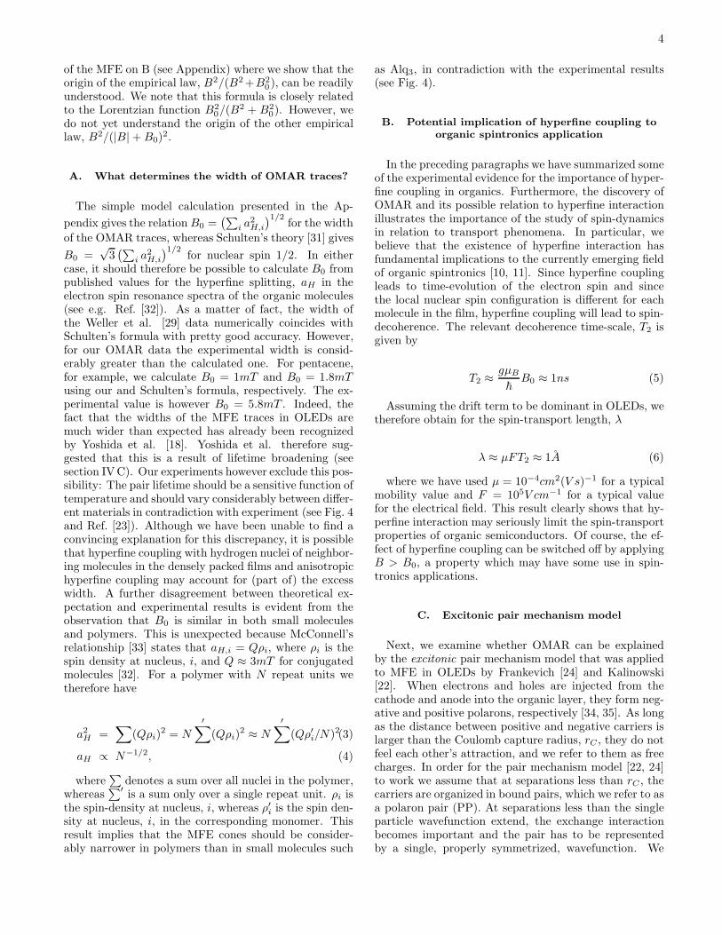
Next, we examine whether OMAR can be explainedby the excitonic pair mechanism model that was appliedto MFE in OLEDs by Frankevich [24] and Kalinowski[22]. When electrons and holes are injected from thecathode and anode into the organic layer, they form neg-ative and positive polarons, respectively [34, 35]. As longas the distance between positive and negative carriers islarger than the Coulomb capture radius, rC , they do notfeel each other’s attraction, and we refer to them as freecharges. In order for the pair mechanism model [22, 24]to work we assume that at separations less than rC , thecarriers are organized in bound pairs, which we refer to asa polaron pair (PP). At separations less than the singleparticle wavefunction extend, the exchange interactionbecomes important and the pair has to be representedby a single, properly symmetrized, wavefunction. We
5
3PP+
C
3PP0 3PP-
Se
Gs
Te
kPS
kPC kPC
kSP
kPT kTP
kCP/4 kCP/4
kSG kGS kTG
kHF0
kHF
kHF
kHF
2J
1PP
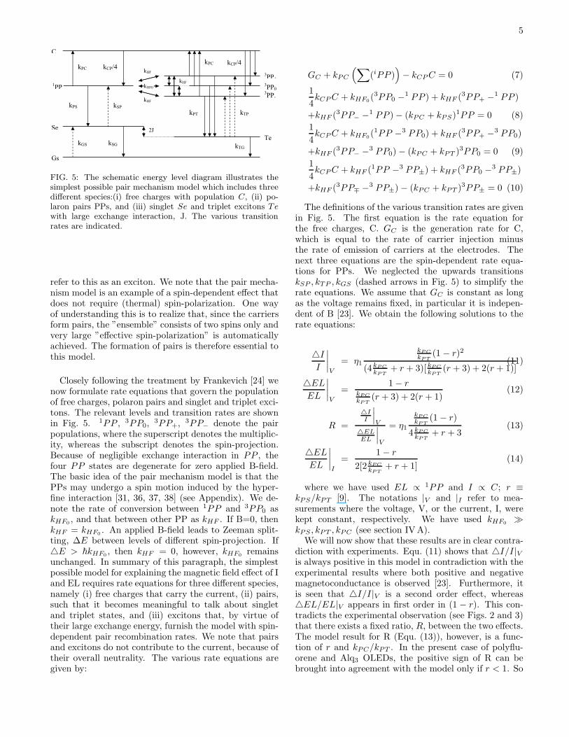
FIG. 5: The schematic energy level diagram illustrates thesimplest possible pair mechanism model which includes threedifferent species:(i) free charges with population C, (ii) po-laron pairs PPs, and (iii) singlet Se and triplet excitons Tewith large exchange interaction, J. The various transitionrates are indicated.
refer to this as an exciton. We note that the pair mecha-nism model is an example of a spin-dependent effect thatdoes not require (thermal) spin-polarization. One wayof understanding this is to realize that, since the carriersform pairs, the ”ensemble” consists of two spins only andvery large ”effective spin-polarization” is automaticallyachieved. The formation of pairs is therefore essential tothis model.
Closely following the treatment by Frankevich [24] wenow formulate rate equations that govern the populationof free charges, polaron pairs and singlet and triplet exci-tons. The relevant levels and transition rates are shownin Fig. 5. 1PP , 3PP0,
3PP+, 3PP− denote the pairpopulations, where the superscript denotes the multiplic-ity, whereas the subscript denotes the spin-projection.Because of negligible exchange interaction in PP , thefour PP states are degenerate for zero applied B-field.The basic idea of the pair mechanism model is that thePPs may undergo a spin motion induced by the hyper-fine interaction [31, 36, 37, 38] (see Appendix). We de-note the rate of conversion between 1PP and 3PP0 askHF0
, and that between other PP as kHF . If B=0, thenkHF = kHF0
. An applied B-field leads to Zeeman split-ting, ∆E between levels of different spin-projection. If△E > ~kHF0
, then kHF = 0, however, kHF0remains
unchanged. In summary of this paragraph, the simplestpossible model for explaining the magnetic field effect of Iand EL requires rate equations for three different species,namely (i) free charges that carry the current, (ii) pairs,such that it becomes meaningful to talk about singletand triplet states, and (iii) excitons that, by virtue oftheir large exchange energy, furnish the model with spin-dependent pair recombination rates. We note that pairsand excitons do not contribute to the current, because oftheir overall neutrality. The various rate equations aregiven by:
GC + kPC
(
∑
(iPP ))
− kCP C = 0 (7)
1
4kCP C + kHF0
(3PP0 −1 PP ) + kHF (3PP+ −1 PP )
+kHF (3PP− −1 PP ) − (kPC + kPS)1PP = 0 (8)
1
4kCP C + kHF0
(1PP −3 PP0) + kHF (3PP+ −3 PP0)
+kHF (3PP− −3 PP0) − (kPC + kPT )3PP0 = 0 (9)
1
4kCP C + kHF (1PP −3 PP±) + kHF (3PP0 −3 PP±)
+kHF (3PP∓ −3 PP±) − (kPC + kPT )3PP± = 0 (10)
The definitions of the various transition rates are givenin Fig. 5. The first equation is the rate equation forthe free charges, C. GC is the generation rate for C,which is equal to the rate of carrier injection minusthe rate of emission of carriers at the electrodes. Thenext three equations are the spin-dependent rate equa-tions for PPs. We neglected the upwards transitionskSP , kTP , kGS (dashed arrows in Fig. 5) to simplify therate equations. We assume that GC is constant as longas the voltage remains fixed, in particular it is indepen-dent of B [23]. We obtain the following solutions to therate equations:
△I
I
∣
∣
∣
∣
V
= η1
kP C
kP T(1 − r)2
(4kP C
kP T+ r + 3)[kPC
kP T(r + 3) + 2(r + 1)]
(11)
△EL
EL
∣
∣
∣
∣
V
=1 − r
kPC
kP T(r + 3) + 2(r + 1)
(12)
R =
△II
∣
∣
∣
V
△ELEL
∣
∣
∣
V
= η1
kP C
kP T(1 − r)
4kP C
kP T+ r + 3
(13)
△EL
EL
∣
∣
∣
∣
I
=1 − r
2[2kPC
kP T+ r + 1]
(14)
where we have used EL ∝ 1PP and I ∝ C; r ≡kPS/kPT [9]. The notations |V and |I refer to mea-surements where the voltage, V, or the current, I, werekept constant, respectively. We have used kHF0
≫kPS , kPT , kPC (see section IV A).
We will now show that these results are in clear contra-diction with experiments. Equ. (11) shows that △I/I|Vis always positive in this model in contradiction with theexperimental results where both positive and negativemagnetoconductance is observed [23]. Furthermore, itis seen that △I/I|V is a second order effect, whereas△EL/EL|V appears in first order in (1 − r). This con-tradicts the experimental observation (see Figs. 2 and 3)that there exists a fixed ratio, R, between the two effects.The model result for R (Equ. (13)), however, is a func-tion of r and kPC/kPT . In the present case of polyflu-orene and Alq3 OLEDs, the positive sign of R can bebrought into agreement with the model only if r < 1. So
6
in the following discussion we will limit ourselves to thiscase. For the sake of discussion, we will study two limits:kPC/kPT ≫ 1 and kPC/kPT ≪ 1. If kPC/kPT ≫ 1, (11)(12) (14) can be simplified as:
∆I
I
∣
∣
∣
∣
V
= η1
(1 − r)2
4kPC
kP T(r + 3)
;∆EL
EL
∣
∣
∣
∣
V
=1 − r
kPC
kP T(r + 3)
∆EL
EL
∣
∣
∣
∣
I
=1 − r
4kP C
kP T
(15)
If kPC/kPT ≪ 1, (11) (12) (14) can be simplified as:
∆I
I
∣
∣
∣
∣
V
= η1
kP C
kP T(1 − r)2
2(r + 1)(r + 3);
∆EL
EL
∣
∣
∣
∣
V
=1 − r
2(r + 1)
∆EL
EL
∣
∣
∣
∣
I
=1 − r
2(r + 1)(16)
From these results it follows that ∆II
∣
∣
Vcan be large
only if kPC ≈ kPT . Whereas this condition could be acci-dentally satisfied in a single material at a single temper-ature, it cannot hold true at all temperatures in differentmaterials. The model’s conclusion that ∆I
I
∣
∣
Vis always
small results because the free charges, the only currentcarrying species in the model, do not directly participatein the spin-dependent reactions or the hyperfine transi-tions. In particular, when kPC/kPT ≫ 1 most polaronsexist as free charges and the pair concentration and there-fore the MFE are small. When kPC/kPT ≪ 1 the pairconcentration and therefore the MFE are large, but thelarge change in the pair population does not affect thecurrent because the pairs do not dissociate. Equs. (15)and (16) highlight another contradiction between modeland experiment: In the present model it makes little dif-ference whether ∆EL/EL is measured while the voltageor current are kept constant, whereas the experimentalresults (Figs. 2 and 3) showed that ∆EL/EL|V is aboutten times bigger than ∆EL/EL|I .
V. EXPERIMENTAL RESULTS, PART II
In this section we determine experimentally whetherOMAR is related to an excitonic effect or not. This ispossible, since η1 that appears in Equ. (12) can be var-ied experimentally by several orders of magnitude. Byvarying the corresponding electrode materials one cancontrol the injection of minority charge carriers, so thatthe exciton formation can be tuned with ideally minimaleffect on the current density, which is determined mostlyby the majority carriers. This can be easily achieved inhole-dominated PFO devices by choosing cathode (topelectrode) materials with different work functions, butit is difficult in practice to fabricate electron-only Alq3
devices with different anode (bottom electrode) materi-als, because efficient electron injection requires reactive
0.1
1
10
10-6
10-5
10-4
10-4
10-3
10-2
10-1
100
101
0 10 20 30 40 50 60
0
20
40
60
80
10-4
10-3
10-2
10-1
100
η1/3
1
η1/2
1 Al
Ca
Au
η1 (arb. units)
(a)
(b)
Au
AlCa
(c)
AuAlCa
voltage(V)
I(µ
A)
EL
(a
rb.
un
its)
I (A)
∆I/I
(%
)
H17C8 C8H17
R R
FIG. 6: a) Magnitude of the magnetoconductance, ∆I/I , inPFO (see inset) as a function of the exicton/carrier ratio η1
at B = 100mT . b) EL as a function of current. c) Current-voltage (I-V) characteristics. All data were obtained at roomtemperature.
metals such as Ca. We found, e.g. in a Ca/Alq3/Ca de-vice, that the bottom Ca electrode oxidizes quickly beforeand/or after evaporating Alq3 on top of it. So, instead ofAlq3 devices we studied a second polymer, MeLPPP (seeFig. 7, inset) in addition to PFO, to show that the con-clusions we draw are not limited to a particular choice ofpolymer. MeLPPP is a suitable choice, because it shows,like PFO devices, large OMAR as well as intense EL.
Three types each of PFO and MeLPPP devices werefabricated and measured using Ca, Al and Au as cath-ode materials. We note that whereas only one set of datapoints for each device is shown, the reported experimentswere repeated several times and very reproducible resultswere obtained. Figs. 6 and 7 show the current-voltage (I-V) characteristics (Figs. 6c and 7c), the measured ELintensity as a function of I (Figs. 6b and 7b), and themagnitude of ∆I/I as a function of η1 (Figs. 6a and 7a).The exciton/carrier ratio, η1 was inferred from the datashown in panels b) where we found that the magnitude ofEL, at a given current, in Ca devices is about one orderof magnitude larger than that in Al devices, and nearlythree orders of magnitude larger than in Au devices. This
7
10-6
10-5
10-4
10-5
10-4
10-3
10-2
10-1
100
101
0 10 20 30 40
0
20
40
60
80
I(µA)
Ca
Ca
Al
Al
Au
η1 (arb. units)
EL (arb. units)
I (A)
Au
0.1
1
1010
-410
-310
-210
-110
0
∆I/I (%)
η1/3
1
(a)
AuAlCa
voltage(V)
(b)
(c)
R
R
R
R
R
R n
FIG. 7: a) Magnitude of the magnetoconductance, ∆I/I , inMeLPPP (see inset) as a function of the exicton/carrier ratioη1 at B = 100mT . b) EL as a function of current. c) Current-voltage (I-V) characteristics. All data were obtained at roomtemperature.
is evidence of the increasing difficulty of electron injec-tion from the cathode into the polymer going from lowwork-function Ca to high work-function Au. This is well-known [1] to result from the mismatch of the cathodework function and the polymer’s conduction band. Cor-respondingly, η is one (three) orders of magnitude lowerin Al (Au) devices compared to Ca devices. Since, η2 andη3 in Equ. (2) are properties of the excitons [39] in eachorganic material, and they do therefore not depend onthe carrier injection efficiency (hence the cathode mate-rials), we simply use η as a measure of the exciton/carrierratio, η1, of the various devices.
Most importantly, Figs. 6a and 7a show that the mag-nitude of ∆I/I increases as η1 increases in both PFO andMeLPPP devices (results for three choices of the currentare shown for each device). At first sight this trend seemsto confirm an excitonic origin of OMAR. However, closerinspection shows that the η1 dependence is much weakerthan expected. Whereas a linear dependence on η1 is ex-pected for an excitonic effect, we find ∆I/I ∝ ηα
1 , with αranging from 1/3 to 1/2. If, however, OMAR is not re-
lated to an excitonic effect, but caused by a direct effectof B on the (mobility of the) free carriers, we would haveexpected no dependence at all, which does not match themeasurement either. However, the observed weak depen-dence can easily be attributed to several possible factors:It is possible that the interface resistance of polymer/Auis larger than that of polymer/Ca resulting in additionalresistance that is not subject to OMAR. Previous stud-ies [40] report that Au indeed leads to a non-Ohmic topcontact, possibly because the wetting of Au and there-fore the physical contact is inferior, or because Au de-position, which has to be evaporated at a much highertemperature than Ca, leads to damage of the underlyingpolymer surface. Moreover, in unipolar devices space-charge limited current conditions occur which are possi-bly unfavorable for OMAR. In bipolar devices, however,the space charge of the two carrier types partially canceleach other. The fact that changing the cathode materialleads to additional effects, rather than merely changingη1, is shown in Figs. 6c and 7c where it is seen that Aucathode devices show a significantly increased device re-sistance, probably due to the above mentioned parasiticresistance contributions. We have however been unableto come up with any probable or improbable explanationhow the dependence on η1 could be sub-linear in an ex-citonic model. We could imagine superlinear behavior, ifthe spin-dependent reactions are bimolecular. Our mea-surements therefore show that OMAR is most likely notrelated to an excitonic effect.
VI. DISCUSSION, PART II
The excitonic pair mechanism model fails to explainthe comprehensive experimental data, but it still suc-ceeds to account for several experimental observations(namely the magnitude and ”universality” of B0) thatwould otherwise be hard to explain with any model thatdoes not involve the nuclear spin. So, it appears that amodel is demanded, which retains some of the features ofthis model, namely the hyperfine interaction coupled tospin-dependent interactions, but applies them to a spin-dependent reaction that directly influences the mobil-ity. The suggestion by Frankevich [24] to consider spin-dependent bipolaron formation [34] appears promising.In the following we will demonstrate that the assumption
that B acts directly on the mobility, µ, correctly repro-duces the experimental data. We are however presentlynot able to identify or formulate a specific mechanismwith the required properties. Such a theory lies far be-yond the scope of the present paper and we hope thatthe scientific community will attempt to formulate sucha theory.
We now wish to discuss the dependence of EL and Ion the mobility. The most general formula for for thecurrent density, J , is:
J = e(pµp − nµn)F (17)
8
where e is the elementary charge, p and n are the den-sity of positive and negative polarons, respectively andµp and µn are their respective mobilities, F is the elec-tric field. All these quantities may in general dependon the position, x. In the case of unipolar transport, Jin OLEDs is often assumed to be given by in the SpaceCharge Limited Current (SCLC) formula:
J =9
8ǫǫ0µ
V 2
d3, (18)
where V is the applied voltage and d is the device thick-ness, ǫ and ǫ0 have their usual meaning. This formulaholds true only in the trap-free limit, in the case of trapsthe term
(
Vd
)
in Equ. (18) must be replaced by a more
general function, f(
Vd
)
[41]. In the following we willassume that the mobility of one type of carrier greatlyexceeds that of the other, specifically µp ≫ µn. Thisassumption is usually fulfilled in OLEDs.
The relation for EL depends on the the relative mag-nitude of recombination time (τrec) and transit time (τt)[42]. The ratio τrec/(τrec + τt) is a measure of the proba-bility that the carrier will transit the device without re-combining with another carrier. For injection-controlledEL (τt < τrec) we obtain:
EL ∝ γjnjp
µnµp(19)
jtotal ≈ jp (20)
∆EL
EL=
∆I
I=
∆µp
µp(21)
γ is the electron-hole recombination constant, which isusually assumed to be given by the Langevin recombina-tion formula [41], γ = e(µn + µp)/ǫǫ0. Equ. (21) showsthat the experimentally observed intimate relation be-tween ∆EL
EL and ∆II naturally follows in a type (i) model.
However, result Equ. (21) implies that the two effectsshould be strictly of equal magnitude, which is not quitethe case experimentally (see Figs. 2 and 3) where ∆EL
EL
is up to twice as big as ∆II . A more general relationship
is therefore required. For the case τnt > τrec > τp
t weobtain:
EL ∝ jn (22)
jtotal ≈ jp (23)
∆EL
EL=
∆µn
µn;∆I
I=
∆µp
µp(24)
Furthermore, for volume controlled EL (τt > τrec [42]),which requires µp ≈ µn, we obtain:
∆EL
EL=
∆µn
∆µp+(
µn
µp
)2
µn
µp(µn
µp+ 1)
∆µp
µp(25)
∆I
I=
∆µn
∆µp+ µn
µp
2µn
µp
∆µp
µp(26)
In summary, a pair mechanism model that acts di-rectly on the current carrying species naturally impliesthe observed intimate relationship between ∆EL/ELand ∆I/I. Furthermore it implies the experimental ob-servation that ∆EL/EL|I ≪ ∆EL/EL|V (see Figs. 2and 3).
VII. CONCLUSION
We have explored the possibility that hyperfine inter-action causes the recently discovered organic magnetore-sistance effect using both experimental data and theo-retical models. Other groups have previously explainedmagnetic field effects on excitonic processes in organicsusing the hyperfine pair mechanism model. We show thatboth kinds of data can be fitted using the same empiricallaws, either of the form B2/(B2 +B2
0) or B2/(|B|+B0)2
dependent on material. The only fitting parameter, B0,assumes values that, at least at first sight, seem typicalof hyperfine interaction. This suggests that OMAR iscaused by hyperfine interaction as well. We succeeded to”derive” the empirical law B2/(B2 + B2
0) from the stan-dard hyperfine Hamiltonian. We also showed that hy-perfine interaction may seriously limit the spin transportlength, which is of primary importance in spintronics ap-plications.
In order to further test the hyperfine interaction hy-pothesis, we examined a pair mechanism model, sug-gested previously by other authors which considers theelectron spin precession caused by the hydrogen nuclearmagnetic field. However, we found several fundamentalcontradictions with the existing experimental data. Thismodel yields only a small and necessarily positive mag-netoconductance effect, whereas experimentally a largeeffect is found, either of positive or negative sign. It isfound that whereas ∆EL/EL is a first order effect, ∆I/Iappears only in second order, in contradiction to the ex-perimental observation that they are of similar magni-tude. In addition, this model cannot account for the ex-perimental observation that ∆EL/EL measured at con-stant voltage greatly exceeds the same effect when mea-sured at constant current. In summary, we find that theexcitonic pair mechanism model failed to explain OMAR,even only qualitatively. We trace the origin of the fail-ure of the model to the fact that it considers the spin-dynamics of polaron pairs, which, in first order, do notcontribute to the current.
By varying the injection efficiency for minority carriersin the devices, we show experimentally that ∆I/I is onlyweakly dependent on the EL quantum efficiency: ∆I/I ∝ηα1 , with α ranging from 1/3 to 1/2. This dependence
is unexpectedly weak if the effect were of an excitonicorigin. This observation strengthens the conclusion fromthe modelling that OMAR is not due to an excitoniceffect.
Making the (presently unjustified) assumption that Bacts directly on the carrier mobility, we found that the
9
qualitative features of both OMAR and the magneticfield effect on the electroluminescence naturally followfrom this assumption. Therefore, we believe that a pairmechanism model acting on the current carriers directlyis a promising direction for a future theory of OMAR.Spin-dependent bipolaron formation is a possible sce-nario.
VIII. APPENDIX: LORENTZIAN SHAPE OF
MAGNETIC FIELD EFFECT TRACES DEDUCED
FROM THE HYPERFINE HAMILTONIAN
Here we will show that the empirical fitting formula∆I/I ∝ B2/(B2 + B2
0) can be substantiated through asimple calculation to be presented in the following. Themodel considers the standard hyperfine Hamiltonian,
H = ω0Sz +a
~
−→S−→I , (27)
containing the electronic Zeeman energy and the hy-perfine interaction between a single electronic and nu-clear dipole. ω0 = gµBB
~, where g ≈ 2 is the electronic
g-factor and µB is the electronic Bohr magneton,−→S and−→
I are the electronic and nuclear spin (assumed to be1/2), respectively, and a is a measure (in units of fre-quency) of the hyperfine interaction strength. The z-axisis chosen to coincide with the direction of B. The Hamil-tonian will be written in matrix form where we use thefollowing basis vectors: | ⇑↑>, | ⇓↑>, | ⇑↓> and | ⇓↓>.The boldface arrow denotes the z-component of the elec-tronic spin, whereas the second arrow denotes that of thenuclear spin. We obtain the following result:
H = ~
ω0
2+ a
40 0 0
0 −ω0
2− a
4
a2
00 a
2
ω0
2− a
40
0 0 0 −ω0
2+ a
4
(28)
It is evident from the form of H that | ⇑↑> and | ⇓↓>are eigenstates and therefore do not evolve with timeother than through the trivial phase factor. However,| ⇓↑> and | ⇑↓> are mixed with each other throughthe off-diagonal matrix element. For simplicity we willnow consider the time evolution of the | ⇑↓> state only.It turns out that a calculation of the time evolution ofthe most general state vector and subsequent averagingover all electronic and nuclear spin orientations leads tosimilar results. To obtain the time evolution operator weperform a matrix exponentiation:
U = exp
(
Ht
i~
)
(29)
Next we calculate the expectation value of Sz as a func-tion of time:
Sz(t) =<⇑↓ U |Sz|U ⇑↓> (30)
We obtain the following result (in units of ~/2):
Sz(t) =ω2
0
ω20 + a2
+a2
ω20 + a2
cos√
ω20 + a2t (31)
Next we consider the case of a pair of spins each ofwhich are subject to a separate Hamiltonian of formEqu. (27). For simplicity we will treat the time-evolutionof the initial state | ⇑↑>1 | ⇑↓>2 only. Since the firstspin is in an eigenstate it will not evolve with time,whereas the second spin’s time evolution will be governedby Equ. (29). We obtain therefore for the total spin (inunits of ~):
S1+2z (t) =
1
2
(
1 +ω2
0
ω20 + a2
+a2
ω20 + a2
cos√
ω20 + a2t
)
(32)
=1
2+
1
2(pP − pAP ) , (33)
where pP and pAP are the probability for finding thepair in a parallel or antiparallel state, respectively. It isseen that S1+2
z (t) oscillates with time and that the peak-
to-peak modulation depth is given by a2
ω2
0+a2 . At large
B, S1+2z (t) remains close to 1 at all times although it
performs a high-frequency (but small-amplitude) oscilla-tion. At small B, the frequency of the oscillation becomessmaller but its amplitude increases. The question ariseswhether the frequency or the amplitude of the oscilla-tion is the correct measure for the ”spin-flip efficiency”.Because experiment shows (see section IVA) that theoscillation frequency is much larger than the pair recom-bination rate, γ, it is the time average of S1+2
z (t) thatenters into the transition rate, specifically we may write:
γ = pP γP + pAP γAP (34)
=
(
1
2+
ω20
2(ω20 + a2)
)
γP +a2
2(ω20 + a2)
γAP (35)
∆γ
γ≡ γ(B) − γ(B = 0)
γ(B = 0)=
ω20
ω20 + a2
γP − γAP
γP + γAP(36)
γP and γAP are the recombination rates for paralleland antiparallel pairs, respectively. For a state initiallyin an antiparallel state γP and γAP have to be exchangedin Equ. (36).
Finally we relate our results to the experimentally re-ported values, aH = ~a
gµB, for the hyperfine coupling
strength:
MFE ∝ B2
B2 + a2H
(37)
10
Schulten and coworkers [36] have shown that if theelectron spin interacts with a large number of nuclearspins (as in the case of organic semiconductors), then theindividual aH,i have to be added in a random-walk-likemanner. The final relation for B0 is therefore:
B0 =
(
∑
i
a2H,i
)1/2
(38)
[1] R. H. Friend, R. W. Gymer, A. B. Holmes, J. H. Bur-roughes, R. N. Marks, C. Taliani, D. D. C. Bradley,D. A. D. Santos, J. L. Bredas, M. Loglund, et al., Nature397, 121 (1999).
[2] S. R. Forrest, Nature 428, 911 (2004).[3] C. J. Brabec, N. S. Sariciftci, and J. C. Hummelen, Adv.
Func. Mat. 11, 15 (2001).[4] P. Peumans, S. Uchida, and S. R. Forrest, Nature 425,
158 (2003).[5] M. Granstrom, K. Petritsch, A. C. Arias, A. Lux, M. R.
Anderson, and R. H. Friend, Nature 395, 257 (1998).[6] C. D. Dimitrakopoulos and P. R. L. Malenfant, Adv. Mat.
14, 99 (2002).[7] D. J. Gundlach, Y. Y. Lin, and T. N. Jackson, IEEE
Electron. Dev. Lett. 18, 87 (1997).[8] M. Shtein, J. Mapel, J. B. Benziger, and S. R. Forrest,
Appl. Phys. Lett. 81, 268 (2002).[9] M. Wohlgenannt, K. Tandon, S. Mazumdar, S. Ramase-
sha, and Z. V. Vardeny, Nature 409, 494 (2001).[10] V. Dediu, M. Murgia, F. C. Matacotta, C. Taliani, and
S. Barbanera, Solid State Commun. 122, 181 (2002).[11] Z. H. Xiong, D. Wu, Z. V. Vardeny, and J. Shi, Nature
427, 821 (2004).[12] B. Hu, Y. Wu, Z. Zhang, S. Dai, and J. Shen, Appl. Phys.
Lett. 88, 022114 (2006).[13] T. L. Francis, O. Mermer, G. Veeraraghavan, and
M. Wohlgenannt, New J. Phys. 6, 185 (2004).[14] O. Mermer, G. Veeraraghavan, T. Francis, and
M. Wohlgenannt, Solid State Commun. 134, 631 (2005).[15] O. Mermer, G. Veeraraghavan, T. L. Francis, and
M. Wohlgenannt, Weak localization and antilocalization
in polymer sandwich devices, cond-mat/0312204 (2003).[16] J. Kalinowski, M. Cocchi, D. Virgili, V. Fattori, and P. D.
Marco, Phys. Rev. B 70, 205303 (2004).[17] A. H. Davis and K. Bussmann, J. Vac. Sci. & Techn. A
22, 1885 (2004).[18] Y. Yoshida, A. Fujii, M. Ozaki, K. Yoshino, and E. L.
Frankevich, Mol. Cryst. Liquid Cryst. 426, 19 (2005).[19] G. Salis, S. F. Alvarado, M. Tschudy, T. Brunschwiler,
and R. Allenspach, Phys. Rev. B 70, 085203 (2004).[20] V. N. Prigodin, N. P. Raju, K. I. Pokhodnya, J. S. Miller,
and A. J. Epstein, Adv. Mat. 14, 1230 (2002).[21] N. P. Raju, T. Savrin, V. N. Prigodin, K. I. Pokhodnya,
J. S. Miller, and A. J. Epstein, J. Appl. Phys. 93, 6799
(2003).[22] J. Kalinowski, M. Cocchi, D. Virgili, P. D. Marco, and
V. Fattori, Chem. Phys. Lett 380, 710 (2003).[23] O. Mermer, G. Veeraraghavan, T. Francis, Y. Sheng,
D. T. Nguyen, M. Wohlgenannt, A. Kohler, M. Al-Suti,and M. Khan, Phys. Rev. B 72, 205202 (2005).
[24] E. Frankevich, A. Lymarev, I. Sokolik, F. Karasz,S. Blumstengel, R. Baughman, and H. Hoerhold, Phys.Rev. B 46, 9320 (1992).
[25] E. Frankevich, A. Zakhidov, K. Yoshino, Y. Maruyama,and K. Yakushi, Phys. Rev. B 53, 4498 (1996).
[26] J. Kalinowski, J. Szmytkowski, and W. Stampor, Chem.Phys. Lett 378, 380 (2003).
[27] R. Xu, A. Husmann, T. F. Rosenbaum, M.-L. Saboungi,J. E. Enderby, and P. B. Littlewood, Nature 390, 57(1997).
[28] U. Scherf and K. Mullen, Makromol. Chem. 112, 489(1991).
[29] A. Weller, F. Nolting, and H. Staerk, Chem. Phys. Lett.96, 24 (1983).
[30] H. Staerk, W. Kuhnle, and A. Weller, Chem. Phys. Lett.118, 19 (1985).
[31] K. Schulten, J. Chem. Phys. 82, 1312 (1984).[32] I. C. Lewis and L. S. Singer, J. Chem Phys. 43, 2712
(1965).[33] H. M. McConnel, J. Chem. Phys. 24, 764 (1956).[34] A. J. Heeger, S. Kivelson, J. R. Schrieffer, and W. P. Su,
Rev. Mod. Phys. 60, 781 (1988).[35] Z. V. Vardeny and X. Wei, Handbook of Conducting Poly-
mers II (Marcel Dekker, New York, 1997), chap. 22.[36] K. Schulten and P. Wolynes, J. Chem. Phys. 68, 3292
(1978).[37] E. Knapp and K. Schulten, J. Chem. Phys. 71, 1878
(1979).[38] U. E. Steiner and T. Ulrich, Chem. Rev. 89, 51 (1989).[39] M. A. Baldo, D. F. O’Brien, M. E. Thompson, and S. R.
Forrest, Phys. Rev. B 60, 14422 (1999).[40] A. J. Campbell and D. Bradley, J. Appl. Phys. 89, 3343
(2001).[41] M. Pope and C. E. Swenberg, Electronic Processes in
Organic Crystals (New York: Clarendon, 1999).[42] J. Kalinowski, J. Phys. D: Appl. Phys. 32, R179 (1999).


