Embed Size (px)
Citation preview

Open Access
Dynamic Device Characteristics and LinewidthMeasurement of InGaN/GaN Laser DiodesVolume 13, Number 1, February 2021
Steffan GwynScott WatsonThomas SlightMartin KnappShaun ViolaPavlo IvanovWeikang ZhangAmit YadavEdik RafailovMohsin HajiKevin E DohertySzymon StanczykSzymon GrzankaPiotr PerlinStephen P NajdaMike LeszczyskiAnthony E Kelly
DOI: 10.1109/JPHOT.2020.3045218

IEEE Photonics Journal Dynamic Device Characteristics
Dynamic Device Characteristics andLinewidth Measurement of InGaN/GaN
Laser DiodesSteffan Gwyn ,1,2 Scott Watson,1 Thomas Slight ,3
Martin Knapp,4 Shaun Viola,1 Pavlo Ivanov,1,3 Weikang Zhang ,1Amit Yadav ,5 Edik Rafailov ,5 Mohsin Haji,4 Kevin E Doherty ,6
Szymon Stanczyk ,7 Szymon Grzanka,7 Piotr Perlin,7Stephen P Najda,7 Mike Leszczyski,7 and Anthony E Kelly1
1School of Engineering, University of Glasgow, Glasgow G12 8LT, U.K.2School of Mathematics and Physics, Queen’s University Belfast, Belfast BT7 1NN, U.K.
3Compound Semiconductor Technologies Global Ltd., Glasgow G72 0BN, U.K.4National Physical Laboratory, Teddington TW11 0LW, U.K.
5Aston University, Birmingham B4 7ET, U.K.6Kelvin Nanotechnology, Glasgow G12 8LS, U.K.
7TopGaN Lasers, 01-142 Warsaw, Poland
DOI:10.1109/JPHOT.2020.3045218
Manuscript received November 20, 2020; revised December 4, 2020; accepted December 11, 2020.Date of publication December 16, 2020; date of current version December 31, 2020. This workwas supported in part by the European Union under Grant E113162, in part by Innovate U.K.under Grant 132543, in part by the National Centre for Research and Development under GrantE113162/NCBiR/2020, and in part by the Engineering and Physical Sciences Research Council RCUKunder Grant EP/L015323/1. (Steffan Gwyn and Scott Watson have contributed equally to this work).Corresponding Author: Steffan Gwyn (e-mail: [email protected]).
Abstract: We report on the characterization and analysis of a GaN-based distributedfeedback laser diode (DFB-LD) with 3rd-order laterally etched sidewall gratings centeredat a wavelength of 420 nm. We also compare the device parameters with two commonlyused Fabry-Perot (FP) devices operating at 450 nm and 520 nm. Intrinsic properties of thedevices were extracted, including damping factor, carrier and photon lifetimes, modulationefficiency, differential gain, and parasitic capacitance. These parameters showed that theDFB exhibits a lower damping rate and parasitic capacitance while demonstrating a highermodulation efficiency, indicating that the DFB shows good potential for communicationsapplications. Additionally, spectral linewidth of a GaN DFB is reported. To the authors’knowledge, this is the first demonstration of parameter extraction and spectral linewidthmeasurement for GaN-based DFB-LDs.
Index Terms: Gallium Nitride, distributed feedback laser diode, optical communications.
1. IntroductionGallium Nitride (GaN)-based devices have been the focal point of significant research interestover the past three decades, since Nakamura demonstrated their value as LEDs [1]. In particular,GaN-based laser diodes (LDs) are a potentially key component in visible light communication(VLC) systems, with higher modulation bandwidth and output power capabilities compared to theirLED counterparts. Standard Fabry-Perot (FP) GaN LDs have shown high bandwidths, allowingcommunication at data rates of multiple gigabits per second [2], [3]. However, for many applications,such as cold atom systems [4], spectroscopy [5], medical diagnostics [6], and underwater optical
Vol. 13, No. 1, February 2021 1500510

IEEE Photonics Journal Dynamic Device Characteristics
communications [7], [8], spectral purity and the ability to select and tune specific wavelengths isextremely important [9]. To address this issue, the development of single-mode GaN-based LDsemitting at blue and green wavelengths have been recently reported [10]–[12]. One major issueobserved in all GaN distributed feedback (DFB) LDs previously reported is the high thresholdcurrent, resulting in thermal degradation issues which can affect device reliability. Additionally,while the basic characteristics of these devices have been reported, the underlying mechanismsthat dictate the behavior of GaN-based DFB LDs have not. This work investigates these deviceproperties through frequency response subtraction analysis, implementing a method first proposedby Morton et al. [13]. By calculating parameters such as the resonance frequency and damping rateof a device, important properties ranging from carrier and photon lifetimes (Tc and Tp, respectively)to differential gain (g’) can be derived. From Tc and Tp, one can deduce how carriers and photonsinteract within the active region, and therefore provide an insight into the internal quantum efficiency(IQE) [14] of the device. Differential gain, on the other hand, is an important parameter in thederivation of modulation efficiency, which indicates the speeds at which an LD can communicatedata, as well as spectral linewidth, understanding of which is vital for the previously mentionedapplications [15]. A narrow spectral linewidth ensures that minimal chromatic dispersion occurs,and for quantum applications such as atomic clocks the linewidth frequency must be narrower thanthe atomic transition being targeted, ensuring that atoms can be cooled efficiently [16]. Whilst theseparameters have been well established in InP [17]–[19] and GaAs [20]–[23] DFB lasers, this is notthe case for GaN devices. GaN LEDs have been the subject of vigorous research in terms of theirrecombination coefficients [24]–[26], while modulation efficiency and differential gain have beenreported only for GaN FPs [27], [28]. This work will better characterize the carrier transport effectsfound in GaN-based DFBs, and indicate where improvements need to occur such that visible lightdevices can compete with the modulation characteristics of more established telecommunicationsLD technologies. Additionally, the results found for the DFB device will be compared to calculatedvalues for commercial blue and green GaN FP devices, to demonstrate the feasibility of GaN-basedlaterally-coupled (LC) DFBs for the applications previously mentioned. These devices have beenwell-investigated by several research groups [2], [27], [29]–[33], and thus provide a benchmark forGaN-based device performance. Through comparison of their extracted parameters, one can drawconclusions as to GaN DFB suitability for applications such as optical communications, where therehave been notable research drives for GaN LD technologies.
Following investigation into parameter extraction methods for GaN DFBs, spectral linewidthmeasurements will be discussed. This is a particularly important parameter for quantum coolingapplications, as well as in communications applications, where a narrow linewidth can allow forprecise wavelength division multiplexed (WDM) systems. This setup would require several devices,with central wavelengths separated by as little as 1 nm, operating in a multiplexed system for highdata rate VLC systems, similar to that described in [31], which is a potential application with suitableoptical filtering [34].
2. Device Properties2.1 DFB Device Structure
Fig. 1 shows the LC-DFB structure, with full fabrication details outlined in [35], [36]. A standardridge waveguide laser diode was originally fabricated, with the following epi-layers, from top tobottom:
� GaN:Mg subcontact layer.� AlGaN:Mg cladding layer.� AlGaN:Mg graded index (GRIN) layer.� GaN spacer layer.� InGaN waveguiding layer.� 2 x InGaN quantum wells, with GaN barriers.� InGaN:Si waveguiding layer.
Vol. 13, No. 1, February 2021 1500510

IEEE Photonics Journal Dynamic Device Characteristics
Fig. 1. Design of a typical GaN-based LC-DFB with a deeply-etched sidewall grating. Note: this diagramis not to scale.
� GaN:Si technical layer.� AlGaN:Si GRIN layer.� AlGaN cladding layer.Gratings were then etched laterally into the sidewall of the ridge, down to the top of the upper
waveguiding layer, at an etch depth of 580 nm, such that a GaN-based LC-DFB could be fullyrealized. This fabrication method was chosen because the complex overgrowth steps required tofabricate a buried heterostructure DFB are not currently possible in GaN [37], and surface gratingscan damage the p-contact [38], resulting in increased losses in areas without electrical pumping.This is one of the more straightforward routes to single-wavelength emission, requiring only a minormodification of a standard ridge waveguide process. The main additional difficulty is the deep andvertical semiconductor etch to form the sidewall notches. 1st-order gratings would be challengingto fabricate at the intended wavelength, as feature sizes of ∼40 nm would be required for emissionat ∼400 nm [33] with etch depths of ∼600 nm. Therefore, a 3rd-order grating was implemented,with feature sizes of ∼120 nm, and an 80% duty cycle to achieve coupling strengths comparableto that observed in a 1st-order grating [39]. The device used was a 3rd-order grating DFB withoutfacet coatings, with a cavity length of 500 µm, and mounted p-side up in a TO5.6 package.
2.2 Device Characterization
Firstly, the LVI characteristics of the device were investigated at a constant temperature of 17 °C,and are shown in Fig. 2(a). The device has a threshold current of 32 mA at a threshold voltageof 8.2 V, and exhibits a differential series resistance of approximately 40 �. This high value is inpart due to the reduced contact area associated with the LC-DFB design. A single-mode outputpower of 11 mW is achieved. Comparing the threshold current to previously reported devices[10]–[12], [35], [36], however, it is markedly lower than what has been observed before, throughwavelength alignment of the gain peak and grating stopband. The reduced threshold current wouldresult in fewer thermal degradation issues, and therefore improve device reliability and lifetime [40].The emission spectra of the device were acquired using a high-resolution 1m-long spectrometer(FHR1000 Horiba Jobin Yvon), a Synapse 2048 x 512 CCD camera, and a 3600 groove-per-mmdiffraction grating, shown in Fig. 2 (b). This setup provides a resolution of ∼6.2 pm for emission ata wavelength of 420 nm, which is an order of magnitude below the expected FP mode spacing inthe GaN device. At 70 mA, mode-hopping behavior is evident, with multiple peaks observable anda wavelength hop to high wavelength. A wavelength hop of around 0.8 nm occurs, the cause ofwhich is unlikely to be related to the DFB stopband, as this would yield a coupling coefficient of κ ≈350 cm−1 [41], which in comparison to the calculated values in [35] is too large. The jump is more
Vol. 13, No. 1, February 2021 1500510

IEEE Photonics Journal Dynamic Device Characteristics
Fig. 2. (a) LVI characteristics of the GaN DFB with increasing bias current. (b) Spectral characteristicsof the GaN DFB with increasing bias current. (c) Frequency Response of the GaN DFB at various biascurrents. (d) Optical -3dB bandwidths with increasing bias current.
likely to arise from the emergence of the first-order transverse mode, since the calculated modalindex changes between the zeroth-order and TE01 modes are consistent with this observed shiftin the DFB stopband. This is also observed in Fig. 2 (a), with kinks visible between 60 and 70 mA.The tuning coefficient of the device with current was measured to be 0.015 nm/mA. In comparison,commercially available FP devices were found to have tuning coefficients of 0.03 nm/mA, and areduced tuning coefficient indicates higher wavelength selectability, and therefore that the devicetested is indeed a DFB.
3. Results and Analysis3.1 Frequency Response
Following steady-state measurements, frequency response measurements were taken. The laserlight was focused onto an ALPHALAS UPD-30-VSG-P Ultrafast photodetector, which has a band-width of 10 GHz. Using this setup, the optical −3 dB bandwidths were calculated at varying biascurrents, and are shown in Fig. 2 (c). There is a rise in the response of the device after 100 MHzdue to inductive peaking between the chip and package [42]. Fig. 2 (d) shows the bandwidth ofthe device plotted against bias current. The maximum bandwidth of 2.1 GHz occurs at 40 mA,and starts to decrease after this. As the bandwidth of the detector is 10 GHz, this is not a likelylimiting factor. Parasitic capacitance within the device and package are the likeliest candidates forthe limitations in this measured bandwidth.
Vol. 13, No. 1, February 2021 1500510

IEEE Photonics Journal Dynamic Device Characteristics
Fig. 3. (a) Subtracted frequency response at varying bias current. (b) Damping factor against the squareof resonant frequency for the GaN DFB. (c) Plot of the square of resonant frequency against bias currentabove threshold for the GaN DFB. (d) Calculated intrinsic and parasitic response for the GaN DFB.
3.2 Parameter Extraction
To remove any effects caused by extrinsic factors such as parasitics, and subsequently acquirethe dynamic device characteristics, parameter extraction was performed as per Morton et al. [13].This has been used extensively in InP and GaAs devices, however to the author’s knowledgehas never been reported in GaN DFB lasers. To remove parasitic effects which remain constantwith bias, the response at low bias current is subtracted from a higher bias and then fitted as in[13]. Typical fits are shown in Fig. 3 (a), with the frequency response at 40 mA being subtractedfrom that at 45 mA, 50 mA and 55 mA. From Fig. 3 (a), there is good agreement between thecalculated fit and experimental data. The remaining response is then fitted to reveal the values ofresonant frequency (fr) and damping rate (γ ) at each bias. The |R|2 value was above 95% for eachcurve, indicating a good fit to the experimental data. The values found for fr and γ are lower thanthose which are typical in AlGaAs or InP-based systems [43]. This arises from the dependency ofresonant frequency on parameters such as differential gain and photon density above threshold[44]. γ is related to fr by γ = K f 2
r + 1/τc[45], where Tc is the effective carrier lifetime in the device,
i.e., the sum of all carrier recombination methods. K is the damping factor of the DFB, which isdirectly related to the photon lifetime Tp as K = 4π2τp [44]. Therefore, by plotting γ against fr2,one can find both the carrier and photon lifetimes for the GaN DFB. This is shown in Fig. 3 (b).Through calculating the gradient and intercept of the line, values of K = 0.23 ns (Tp = 5.83 ps), andTc = 0.25 ns were found. These values are similar to that found for InP lasers [43], while the carrierlifetime found is an order of magnitude lower than that for previous work in the GaN material system[28]. This may be due to increased non-radiative recombination due to the larger surface area in
Vol. 13, No. 1, February 2021 1500510

IEEE Photonics Journal Dynamic Device Characteristics
Fig. 4. (a) Comparison of Fig 3(b) for the GaN DFB against two commercial GaN FPs, one OSRAMPL450B and one ORSAM PL520B. (b) Comparison of Fig 4(a) for the same devices as in (a).
the grating. A relation can also be found between bias current and resonant frequency through theequation f 2
r = D(I − It h), where
D = ηvg�g′
4π2Ve(1)
is the square of the modulation efficiency of the device [38]. Here, η is the IQE, vg is the groupvelocity, � is the confinement factor, V is the active volume and e is the electron charge. Fig. 3(c) shows the square of resonant frequency against current above threshold. Using the gradient ofthe line in Fig. 3 (c), it is found that D = 0.51 GHz2/mA, corresponding to a modulation efficiencyof 0.71 GHz/mA0.5. From here, using known values for constants contained within D [40], as wellas values calculated for vg, �, and V through simulations using RSoft’s LaserMOD software tool,a differential gain of g’ = 7.42 × 10⁻¹⁶ cm2 was estimated. For lasers in more well establishedmaterials such as InP and GaAs, D and g’ are typically an order of magnitude higher [18], [22],[23], however in previous reported works for GaN FP devices, D was found to be significantlylower, ranging from ∼0.1 GHz/mA0.5 [27] to ∼0.5 GHz/mA0.5 [28]. Finally, from the values found forfr and γ , the intrinsic response was found for the GaN DFB. The intrinsic response and subsequentparasitic response, which is equivalent to the calculated intrinsic response subtracted from theexperimental results, is shown in Fig. 3 (d). The parasitic response remains constant with increasingbias. Using calculated values for series resistance of the device, the parasitic capacitance wasfound to be 7.7 pF. High speed operation (>10 GHz) requires the parasitic capacitance to bean order of magnitude lower [46], as well as a reduction in series resistance. The intrinsic 3 dBbandwidths increase with bias current, and intrinsic bandwidths up to 5.87 GHz were found for thedevice at 55 mA, suggesting 10 Gbit/s direct modulation may be possible.
3.3 Comparison With Commercial Devices
The previous experiments were also undertaken for one blue GaN FP device, an OSRAM PL450Bcentered at 450 nm, and one green GaN FP device, an OSRAM PL520B centered at 520 nm.These devices have been consistently researched for their properties, and as such are a notablebenchmark to compare a GaN-based DFB to. Following parameter extraction, comparisons canbe drawn between the DFB and commercial devices. Fig. 4(a) shows the plot used to calculatecarrier and photon lifetimes as before in Fig. 3(b), but for the DFB and commercial FPs. From Fig.4(a), the value of the damping rate K, and therefore the photon lifetime, is much smaller for theDFB compared to the FPs, with photon lifetimes of 20.4 ps and 38 ps for the blue and green FPsrespectively, compared to 5.8 ps for the DFB. Additionally, the carrier lifetime calculated for the blueFP and green FP is 0.87 ns and 0.37 ns respectively, while the DFB exhibits a carrier lifetime of 0.25
Vol. 13, No. 1, February 2021 1500510
IEEE Photonics Journal Dynamic Device Characteristics
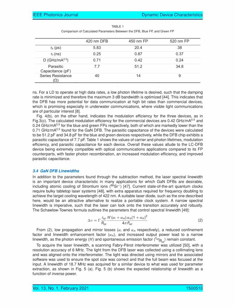
TABLE 1
Comparison of Calculated Parameters Between the DFB, Blue FP, and Green FP
ns. For a LD to operate at high data rates, a low photon lifetime is desired, such that the dampingrate is minimized and therefore the maximum 3 dB bandwidth is optimized [44]. This indicates thatthe DFB has more potential for data communication at high bit rates than commercial devices,which is promising especially in underwater communications, where visible light communicationsare of particular interest [8].
Fig. 4(b), on the other hand, indicates the modulation efficiency for the three devices, as inFig.3(c). The calculated modulation efficiency for the commercial devices are 0.42 GHz/mA0.5 and0.24 GHz/mA0.5 for the blue and green FPs respectively, both of which are markedly lower than the0.71 GHz/mA0.5 found for the GaN DFB. The parasitic capacitance of the devices were calculatedto be 51.2 pF and 34.8 pF for the blue and green devices respectively, while the DFB chip exhibits aparasitic capacitance of 7.7 pF. Table 1 shows the values of carrier and photon lifetimes, modulationefficiency, and parasitic capacitance for each device. Overall these values allude to the LC-DFBdevice being extremely compatible with optical communications applications compared to its FPcounterparts, with faster photon recombination, an increased modulation efficiency, and improvedparasitic capacitance.
3.4 GaN DFB Linewidths
In addition to the parameters found through the subtraction method, the laser spectral linewidthis an important device characteristic in many applications for which GaN DFBs are desirable,including atomic cooling of Strontium ions (88Sr+) [47]. Current state-of-the-art quantum clocksrequire bulky tabletop laser systems [48], with extra apparatus required for frequency doubling toachieve the target cooling wavelength of 422 nm. A suitable laser diode, such as the one describedhere, would be an attractive alternative to realize a portable clock system. A narrow spectrallinewidth is imperative, such that the laser can lock onto the transition accurately and robustly.The Schawlow-Townes formula outlines the parameters that control spectral linewidth [49]:
ν = �rsp
Rsp
hf (αi + αm ) αm(1 + αH )2
4πPout(2)
From (2), low propagation and mirror losses (αi and αm respectively), a reduced confinementfactor and linewidth enhancement factor (αH ), and increased output power lead to a narrowlinewidth, as the photon energy (hf ) and spontaneous emission factor (rsp/Rsp
) remain constant.
To acquire the laser linewidth, a scanning Fabry-Pérot interferometer was utilized [50], with aresolution accuracy of 6 MHz. The light from the DFB laser was collected using a collimating lensand was aligned onto the interferometer. The light was directed using mirrors and the associatedsoftware was used to ensure the spot size was correct and that the full beam was focused at theinput. A linewidth of 18.7 MHz was acquired for a similar device to what was used for parameterextraction, as shown in Fig. 5 (a). Fig. 5 (b) shows the expected relationship of linewidth as afunction of inverse power.
Vol. 13, No. 1, February 2021 1500510

IEEE Photonics Journal Dynamic Device Characteristics
Fig. 5. (a) GaN DFB Laser linewidth using scanning Fabry-Pérot interferometry, with system uncertain-ties highlighted in brackets. (b) Relation of linewidth with inverse optical power for the GaN DFB.
Typically, linewidth of the order of ∼1 MHz are required for atomic cooling applications. As GaNDFBs are a relatively new technology, these spectral linewidths are currently being optimized inorder to fully realize their suitability for quantum applications.
3.5 Improvements to GaN DFBs
To improve the high-speed modulation capabilities, the differential gain needs to be increased, anddevice length should be reduced. Differential gain improvements could be achieved by improvementin material quality and increasing the number of wells and hence confinement factor. Reducedlength whilst maintaining DFB operation requires an increase in coupling coefficient κ, which isdifficult to achieve in LC-DFBs. Changing the grating width [26] or depth to increase κ is possiblein this case, but the upper value of coupling coefficient is limited by the maximum achievable indexchange via this grating geometry. A buried grating would be desirable, but as previously mentionedthe overgrowth steps required are not feasible in GaN. Further improvements may require epitaxialdesign changes.
In terms of spectral linewidth, atomic cooling applications require <1 MHz linewidth [4] whichrequires significant improvements over current performance. These could be achieved through theapplication of dielectric facet coatings, reduction of cavity loss, the use of grating phase shifts, andthe general improvement of laser performance to increase output power. Ideally, the range at whichthe device works in single mode operation will be increased, allowing measurements at higherpowers and ultimately resulting in lower linewidths.
4. ConclusionIn this work, intrinsic parameters of GaN laser diodes were ascertained for the first time. ThreeGaN-based LDs, one DFB and two commercial FPs, were characterized, and the intrinsic responseof the devices were determined. The damping factor, carrier and photon lifetime, modulation effi-ciency, differential gain and parasitic capacitance were all calculated, with improved performanceshown by the DFB compared to the FPs. The results were also comparable to those found inmore well-established telecommunications lasers. This indicates the possibility of high-speed directmodulation of single-frequency blue lasers.
AcknowledgementThe authors would like to thank Dr Guilong Huang for their assistance in the experimental setup
for linewidth measurement.
Vol. 13, No. 1, February 2021 1500510
IEEE Photonics Journal Dynamic Device Characteristics
References[1] S. Nakamura, T. Mukai, and M. Senoh, “Candela-class high-brightness InGaN/AlGaN double-heterostructure blue-
light-emitting diodes,” Appl. Phys. Lett., vol. 64, pp. 1687–1689, 1994.[2] S. Watson et al., “Visible light communications using a directly modulated 422 nm GaN laser diode,” Opt. Lett., vol. 38,
pp. 3792–3794, 2013.[3] W. S. Tai, H. H. Lu, H. W. Wu, C. W. Su, and Y. C. Huang, “A 30 Gb/s PAM4 underwater wireless laser transmission
system with optical beam reducer/expander,” Sci. Rep., vol. 9, 2019, Art. no. 8605.[4] A. Shiner, “Development of a frequency stabilized 422-nm diode laser system and its application to a 88Sr+single ion
optical frequency standard,” MSc Thesis, Dept. Faculty Graduate Sci., York University, Toronto, 2006.[5] B. Li et al., “Sensitive Raman gas analysis using a 500mW external cavity diode laser at 410 nm,” Laser Phys. Lett.,
vol. 14, 2017, Art. no. 095701.[6] S. P. Najda et al., “A multi-wavelength (u.v. to visible) laser system for early detection of oral cancer,” in Imag.,
Manipulation, Anal. Biomolecules, Cells Tissues XIII: Proc. SPIE Photon. West, San Fransisco, USA, Sep.-Nov. Feb.2015, ed., D. L. Farkas, D. V. Nicolau, and R. C. Leif, SPIE, Bellingham, USA, 2015, pp. 50–55.
[7] T. C. Wu, Y. C. Chi, H. Y. Wang, C. T. Tsai, and G. R. Lin, “Blue laser diode enables underwater communication at 12.4Gbps,” Sci. Rep., vol. 7, 2017, Art. no. 408040.
[8] G. Giuliano, L. Laycock, D. Rowe, and A. E. Kelly, “Solar rejection in laser based optical communication systems,” Opt.Exp., vol. 25, 2017, Art. no. 33066.
[9] Y. Shimada et al., “A simplified 461-nm laser system using blue laser diodes and a hollow cathode lamp for lasercooling of Sr,” Rev. Sci. Instrum., vol. 84, 2013, Art. no. 063101.
[10] H. Zhang et al., “Continuous-wave operation of a semipolar InGaN distributed-feedback blue laser diode with a first-order indium tin oxide surface grating,” Opt. Lett., vol. 44, 2019, Art. no. 3106.
[11] J. A. Holguín-Lerma, T. K. Ng, and B. S. Ooi, “Narrow-line InGaN/GaN green laser diode with high-order distributed-feedback surface grating,” Appl. Phys. Exp., vol. 12, 2019.
[12] J. H. Kang et al., “DFB laser diodes based on GaN using 10th order laterally coupled surface gratings,” IEEE Photon.Technol. Lett., vol. 30, pp. 231, 2018.
[13] P. Morton, T. Tanbun-Ek, R. Logan, A. Sergent, P. Sciortino, and D. Coblentz, “Frequency response subtraction forsimple measurement of intrinsic laser dynamic properties,” IEEE Photon. Technol. Lett., vol. 4, pp. 133–136, 1992.
[14] S. Karpov, “ABC-model for interpretation of internal quantum efficiency and its droop in III-Nitride LEDs: A review,”Opt. Quantum Electron., vol. 47. pp. 1293–1303, 2015.
[15] Y. Arakawa and A. Yariv, “Theory of gain, modulation response, and spectral linewidth in AlGaAs quantum well lasers,”IEEE J. Quantum Electron., vol. 21, pp. 1666–1674, 1985.
[16] W. D. Phillips, “Nobel Lecture: Laser cooling and trapping of neutral atoms,” Rev. Mod. Phys., vol. 70, p. 721, 1998.[17] H. Lipsanen, D. L. Coblentz, R. A. Logan, R. D. Yadvish, P. A. Morton, and H. Temkin, “High-speed InGaAs/InP
multiple-quantum-well laser,” IEEE Photon. Technol. Lett., vol. 4, p. 673, 1992.[18] O. K. Kwon, C. W. Lee, Y. A. Leem, K. S. Kim, S. H. Oh, and E. S. Nam, “1.5-μm and 10-Gbs−1 etched mesa buried
heterostructure DFB-LD for datacenter networks,” Semicond. Sci. Technol., vol. 30, 2015, Art. no. 105010.[19] T. Sadeev, D. Arsenijevic, and D. Bimberg, “Comparison of dynamic properties of InP/InAs quantum-dot and quantum-
dash lasers,” Appl. Phys. Lett., vol. 109, 2016, Art. no. 161104.[20] L. Bjerkan, A. Royset, L. Hafskjaer, and D. Myhre, “Measurement of laser parameters for simulation of high-speed
fiberoptic systems,” J. Lightw. Technol., vol. 14, p. 839, 1996.[21] R. Nagarajan, T. Fukushima, S. W. Corzine, and J. E. Bowers, “Effects of carrier transport on high-speed quantum well
lasers,” Appl. Phys. Lett., vol. 59, 1991, Art. no. 1835.[22] H. Cantú, A. McKee, D. Childs, S. Watson, and A. E. Kelly, “Dynamic performance of detuned ridge waveguide
AlInGaAs distributed feedback laser diodes,” Microw. Opt. Technol. Lett., vol. 59, 2017, Art. no. 1468.[23] J. D. Ralston et al., “Control of differential gain, nonlinear gain and damping factor for high-speed application of GaAs-
based MQW lasers.,” IEEE J. Quantum Electron., vol. 29, 1993, Art. no. 1648.[24] R. P. Green, J. J. D. McKendry, D. Massoubre, E. D. Gu, M. D. Dawson, and A. E. Kelly, “Modulation bandwidth
studies of recombination processes in blue and green InGaN quantum well micro-light-emitting diodes,” Appl. Phys.Lett, vol. 102, 2013, Art. no. 091103.
[25] T. Lin, H. C. Kuo, X. D. Jiang, and Z. C. Feng, “Recombination pathways in green InGaN/GaN multiple quantum wells,”Nanoscale Res. Lett., vol. 12, p. 137, 2017.
[26] S. Lin, H. Cao, J. Li, X. Sun, H. Xiu, and L. Zhao, “Modulation and optoelectronic properties of GaN-based light-emittingdiodes on GaN template,” Appl. Phys. Exp., vol. 11, 2018, Art. no. 122101.
[27] C. Lee et al., “4 Gbps direct modulation of 450 nm GaN laser for high-speed visible light communication,” Opt. Exp.,vol. 23, 2015, Art. no. 16232.
[28] W. G. Scheibenzuber, U. T. Schwarz, L. Sulmoni, J. Dorsaz, J.-F. Carlin, and N. Grandjean, “Recombination coefficientsof GaN-based laser diodes,” J. Appl. Phys., vol. 109, 2011, Art. no. 093106.
[29] G. Li, F. Hu, P. Zou, C. Wang, G. R. Lin, and N. Chi, “Beyond 10 Gbps 450-nm GaN laser diode based visible lightcommunication system utilizing probabilistic shaping bit loading scheme,” in Proc. 12th Int. Symp. Commun. Syst.,Netw. Digit. Signal Process., 2020, pp. 1–4.
[30] H. M. Oubei et al., “Wireless optical transmission of 450 nm, 3.2 Gbit/s 16-QAM-OFDM signals over 6.6 m underwaterchannel,” in Proc. Conf. Lasers Electro-Opt., 2016, Paper SW1F.1.
[31] H. Chun, A. Gomez, C. Quintana, W. Zhang, G. Faulkner, and D. O’Brien, “A wide-area coverage 35Gb/s visible lightcommunications link for indoor wireless applications,” Sci. Rep., vol. 9, 2019, Art. no. 4952.
[32] D. Tsonev, S. Videv, and H. Haas, “Towards a 100 Gb/s visible light wireless access network,” Opt. Exp., vol. 23, 2019,Art. no. 1627.
Vol. 13, No. 1, February 2021 1500510

IEEE Photonics Journal Dynamic Device Characteristics
[33] G. He, Z. Lv, C. Qiu, and Z. Liu, “Performance evaluation of 520 nm laser diode underwater wireless opticalcommunication systems in the presence of oceanic turbulence,” SID Symp. Dig. Tech. Papers, vol. 51, pp. 47–50,2020.
[34] S. Gwyn et al., “GaN-based distributed feedback laser diodes for optical communications,” in Proc. 4th Int. Conf. Appl.Opt. Photon., 2019, Art. no. 112070O.
[35] T. J. Slight, O. Odedina, W. Meredith, K. E. Docherty, and A. E. Kelly, “InGaN/GaN distributed feedback laser diodeswith deeply etched sidewall gratings,” IEEE Photon. Technol. Lett., vol. 28, pp. 2886–2888, 2016.
[36] T. J. Slight et al., “Continuous-wave operation of (Al,In)GaN distributed-feedback laser diodes high high-order notchedgratings,” Appl. Phys. Exp., vol. 11, 2018.
[37] D. Hofstetter, R. L. Thornton, L. T. Romano, D. P. Bour, M. Kneissl, and R. M. Donaldson, “Room-temperature pulsedoperation of an electrically injected InGaN/GaN multi-quantum well distributed feedback laser,” Appl. Phys. Lett.,vol. 73, 1998, Art. no. 2158.
[38] S. J. Pearton, J. W. Lee, J. D. MacKenzie, C. R. Abernathy, and R. J. Shul, “Dry etch damage in InN, InGaN, andInAlN,” Appl. Phys. Lett., vol. 67, 1995, Art. no. 2329.
[39] D. Pierscinska et al., “Examination of thermal properties and degradation of InGaN-based diode lasers by thermore-flectance spectroscopy and focused ion beam etching,” AIP Adv., vol. 7, 2017, Art. no. 075107.
[40] Y. L. Cao et al., “Hybrid III-V/silicon laser with laterally coupled Bragg grating,” Opt. Exp., vol. 23, pp. 8800–8808, 2015.[41] K. Kihara, H. Soda, H. Ishikawa, and H. Imai, “Evaluation of the coupling coefficient of a distributed feedback laser
with residual facet reflectivity,” J. Appl. Phys., vol. 62, pp. 1526–1527, 1987.[42] J. P. Babic, A. R. Totovic, J. V. Crnjanski, M. M. Krstic, M. L. Mašanovic, and D. M. Gvozdic, “Enhancement of the
MQW-RSOA.s small signal modulation bandwidth by inductive peaking,” J. Lightw. Technol., vol. 37, pp. 1981–1989,2019.
[43] I. Tomkos, I. Roudas, R. Hesse, N. Antoniades, A. Boskovic, and R. Vodhanel, “Extraction of laser rate equationsparameters for representative simulation of metropolitan-area transmission systems and networks,” Opt. Comm.,vol. 194, pp. 109–129, 2001.
[44] A. J. Millard, “High-speed modulation of semiconductor lasers and properties of silver-coated quantum-dot lasers,”M.Sc. Thesis, Dept. Elect. Comput. Eng., University of Illinois at Urbana-Champaign, Urbana, 2010.
[45] C. Reese, E. Yablonovitch, S. Keller, B. Keller, and S. DenBaars, “Absolute internal quantum efficiency of anInGaN/GaN quantum well,” in Proc. Conf. Lasers Electro.-Opt., Anaheim, CA, USA, 1996, p. 472.
[46] H. I. Cantú, A. McKee, I. Eddie, and A. E. Kelly, “Frequency selectivity in directly modulated distributed feedback lasertransmission operation using and impedance match tuning network,” IEEE J. Quantum Electron., vol. 50, pp. 106–111,2014.
[47] S. Watson et al., “Distributed feedback lasers for quantum cooling applications,” in Proc. 22nd Int. Conf. TransparentOpt. Netw., 2020, pp. 1–4.
[48] A. D. Ludlow, M. M. Boyd, J. Ye, E. Peik, and P. O. Schmidt, “Optical atomic clocks,” Rev. Mod. Phys., vol. 87,pp. 637–701, 2015.
[49] C. Henry, “Theory of the phase noise and power spectrum of a single mode injection laser,” IEEE J. Quantum Electron.,vol. 19, pp. 1391–1397, 1983.
[50] T. Takakura, K. Iga, and T. Tako, “Linewidth measurement of a single longitudinal mode AlGaAs laser with a Fabry-Perotinterferometer,” Jpn. J. Appl. Phys., vol. 19, 1980, Paper L725.
Vol. 13, No. 1, February 2021 1500510


