Embed Size (px)
Citation preview

Ta
RKa
b
c
a
ARR1AA
KMTSFL
1
bbtqmaeaMsa(aat
NB
0d
Sensors and Actuators A 174 (2012) 58– 68
Contents lists available at SciVerse ScienceDirect
Sensors and Actuators A: Physical
j ourna l h o me pa ge: www.elsev ier .com/ locate /sna
hermal management of fully LTCC-packaged Cs vapour cell for MEMStomic clock
.K. Chutania,∗, S. Gallioua, N. Passillya, C. Goreckia, A. Sitomaniemib, M. Heikkinenb,
. Kautiob, A. Keränenb, A. Jornodc
Institut FEMTO-ST, CNRS (UMR 6174), Université de Franche Comté, ENSMM, 25044 Besanc on, FranceVTT Technical Research Centre of Finland, P.O. Box 1100, 90571 Oulu, FinlandASULAB, division of The Swatch Group Research and Development Ltd, 2074 Marin, Switzerland
r t i c l e i n f o
rticle history:eceived 28 July 2011eceived in revised form8 November 2011ccepted 21 November 2011vailable online 19 December 2011
eywords:
a b s t r a c t
This paper describes a study of the thermal behaviour of fully packaged Caesium vapour cell developedin the framework of the European collaborative research project called “MEMS atomic clocks for timing,frequency control and communications (MAC-TFC)”. This cell, along with various electronic and opticalcomponents, is embedded in a Low Temperature Co-fired Ceramics (LTCC) structure, in order to build acompact MEMS-based atomic clock. Functioning of such atomic clock depends on inner and outer envi-ronment of the Cs vapour cell, including parameters such as pressure and temperature of buffer gas. Thispaper is then devoted to study the thermal behaviour of a fully LTCC-packaged Cs vapour cell according to
EMS atomic clockhermal behaviourteady state analysisinite element methodTCC packaging
the ambient temperature change when it is locally temperature controlled. Simulations have been carriedout by using analytical modelling and finite element based softwares. Different solutions concerning theLTCC structure such as bridges/suspensions, vacuum environment, metallic coating, as well as the optimalpositions of the temperature-control elements have been investigated. Finally, preliminary experimentsbased on a prototype resulting from this study are presented and an additional solution based on thedynamic adjustment of the set temperature as a function of the ambient temperature is proposed.
. Introduction
Atomic clocks are used as frequency references for a large num-er of applications. They provide enhanced accuracy and stabilityecause their resonance frequency is determined by the energyransition of the atoms, and are consequently more stable thanuartz-based clocks (especially at longer times). Nowadays, sinceore and more applications become mobile, the demand for small
nd low-power clocks is increasing. Thus, scientists focus theirffort on the miniaturised version of the atomic clock, better knowns chip scale atomic clock (CSAC) or MEMS atomic clock (MAC).ACs have consequently rapidly progressed since their first ver-
ion proposed by Kitching et al. [1]. The European project “MEMStomic clock for timing, frequency control and communicationsMAC-TFC)” [2], aims to develop a miniaturised and low power
tomic clock (<150 mW), presenting a fractional frequency devi-tion better than 6 × 10⁻¹⁰ �−1/2 for an integration time � shorterhan one hour, and better than 1 × 10⁻¹¹ �−1/2 for longer time. Its∗ Corresponding author at: Institut FEMTO-ST (UMR 6174), Département Microano Sciences & Systèmes, UFR Sciences et Techniques, Route de Gray, 25030esanc on Cedex, France. Tel.: +33 381666162; fax: +33 38 1666423.
E-mail address: [email protected] (R.K. Chutani).
924-4247/$ – see front matter © 2011 Elsevier B.V. All rights reserved.oi:10.1016/j.sna.2011.11.025
© 2011 Elsevier B.V. All rights reserved.
central element is made of an Alkali vapour cell (a Caesium cell,Cs-cell) excited by a laser beam whose wavelength is locked on theCs atomic hyperfine transition frequency which actually defines thereference frequency �0 = 9.192 631 770 GHz. The locking is achievedby coherent population trapping (CPT) spectroscopy [3]. The latteris particularly suitable because it does not require implementa-tion of a microwave cavity since probing of the atomic resonance isdirectly realised by the laser beam thanks to a destructive quan-tum interference phenomenon. Consequently, it makes possiblethe further reduction in the size of cell and thus reduction of clockvolume.
In the framework of MAC-TFC, alkali vapour micro-cells, madefrom MEMS fabrication techniques and based on compact cav-ities etched in a Si-wafer and sealed by anodic bonding withtwo borosilicate glass wafers, have been successfully fabricated[4–6]. Such vapour cells have dimensions: length (6 mm) × width(4 mm) × thickness (2.4 mm). Therefore, it has been chosen toembed the Cs-cell and the different components of the clock (VCSEL,detector, micro-optical components, etc.) in a Low Temperature Co-fired Ceramics (LTCC) structure, which is highly suitable for hybrid
3D integration. LTCC is a well-established multi-layer technology,featuring the ability to integrate various elements (heaters, sensors,electronics, wires, shielding) in one module only, with high reliabil-ity, stability and alignment accuracy [7]. In the case of MACs, where
nd Ac
mtl
fcvwlcgotbaoafiotoNtsormiottp
LgpmmFStetopS
2
2
bitabis
pwaat
R.K. Chutani et al. / Sensors a
agnetic and thermal environment have to be controlled, LTCCechnology will allow to achieve a high level of miniaturisation withow processing costs.
This structure has then to be temperature controlled since VCSELrequency and various properties of CPT resonances in Cs vapourells are temperature dependent [8]. Indeed, because of the meanelocity of the Cs atoms (typically 230 ms−1 at 60 ◦C) in comparisonith the cavity dimensions (order of magnitude: 1 mm), the CPT
ine-width is easily broadened. Thus, the frequency stability of thelock cannot be achieved without the addition of a so-called bufferas (usually N2, He, Ne, Ar) [9,10]. The buffer gas is then required inrder to prevent wall relaxation, to increase the atom–light interac-ion and to reduce the Doppler broadening. However, interactionsetween caesium atoms and buffer gas introduce a shift of thetomic hyperfine transition frequency. This phenomenon dependsn the nature of the gas, pressure and temperature according to
two order polynomial law [3]. In general, the resulting thermalrequency sensitivity is too high and, thus, a mixture of two gasesnducing opposite linear frequency-shifts is required (i.e. by meansf a compensation method: Ar and Ne for example). Recently, inhe framework of MAC-TFC, a quadratic temperature dependencef the Cs ground state hyperfine resonance frequency in a singleeon buffer gas has been observed [11]. The relatively low inversion
emperature, around 80 ◦C, allows using one gas only and relaxeslightly the constraints onto the cell fabrication and, in particular,n the pressure control. Nevertheless, the thermal managementemains a challenging part since the temperature of the cell must beaintained to within few hundreds of millikelvins at all times dur-
ng operation, using as little power as possible, although the rangef ambient temperature can be 0 to 55 ◦C. Then, a reasonable aim forhe temperature sensitivity of the Cs-cell to the ambient tempera-ure, once the temperature-control operates, is several millikelvinser Kelvin.
In this paper, a thermal management approach considering aTCC-based structure is presented. Several solutions are investi-ated in order to achieve a low-power temperature control. Theaper is organised as follows. In Section 2, we present the thermalanagement approach with respect to the power budget. Ther-al simulations using the MEMS software tool Intellisuite and the
loTHERM computational fluid dynamics software are described inection 3, and show that our solutions provide in steady-state a fineemperature distribution in the area of the cell. After preliminaryxperiments to estimate the power consumption, done with a pro-otype involving few of our propositions, a final approach basedn the dynamic adjustment of the electronically driven set tem-erature as a function of the ambient temperature is proposed inection 4.
. Thermal management approach
.1. Problem and concept
Basically, the MAC is made of several components that have toe temperature controlled. The Cs-cell, i.e., the heart of the clock,
s surrounded by opto-electronic components (VCSEL and pho-odetector) to produce and detect the modulated optical beam,s well as optical components for shaping and polarizing theeam, and electronics to close the feedback loop of the modulat-
ng signal (Fig. 1). All these components are packaged in a LTCCtructure.
The objective is then to maintain the inner temperature of thehysics package constant whatever the external temperature is,
ithin a determined range. The latter changes depending on thepplications of the atomic clock and should be ideally as larges [−40 ◦C, 60 ◦C] [12] or even [−40 ◦C, 70 ◦C] [13]. The defini-ion of this range is actually essential because it fixes the thermal
tuators A 174 (2012) 58– 68 59
management approach and the amount of required power. For arough assessment, the inner target temperature (in K) can be writ-ten as:
Tset = Tamb + R × (Pelec + PT-control) (1)
where Tamb is in Kelvins, Pelec (in W) is the power dissipated by theelectronics (assumed to be a constant) located inside the volume tobe temperature-controlled, PT-control (in W) is the controlled power(0 ≤ PT-control ≤ PT-control Max) dissipated by the heaters in order tomaintain the inner temperature of the volume at Tset independentlyof the value of Tamb. Finally, R (in K W−1) denotes the overall thermalresistance of the system, from its heart at Tset to its surrounding atTamb.
At first sight, it sounds reasonable to insulate as much aspossible the physics package to reduce the power consumption.Indeed, when the ambient temperature is very low (for instanceTamb = −40 ◦C), the overall thermal resistance R should be high inorder to consume as little power as possible (PT-control) and maintainan uniform temperature distribution inside the package. However,the waste heat generated by the embedded electronics cannot beignored. Because of it (Pelec), high overall thermal resistance, i.e.,well insulated packages, can lead to overheating of the cell, if theambient temperature is high. Thus, in this case, the overall thermalresistance (R) should be low, since the maximum ambient tempera-ture is defined by Tset − R × Pelec. As a consequence, practically, such“ideal” ranges are difficult to achieve if one wants meanwhile tostrongly reduce the power consumption. Indeed, for this purpose,it could be tempting to use a lot of waste heat coming from theembedded electronics (for lower ambient temperatures), but forhigh ambient temperatures, the waste heat has to be evacuated,thus R cannot be very high. After preliminary studies, obtained atroom temperature [12,14] and in order to evaluate the solutionsrequired to contain the power budget (among which utilisation ofwaste power), more complicated devices utilizing waste heat weredeveloped. They include, e.g., variable thermal resistors made ofan array of suspended thin gold beams electrostatically actuated[15], or thermal switches made of a bimetallic buckling disk [16]in order to change, actively or passively respectively, the thermalresistance as a function of the ambient temperature. Although thesesolutions could allow to reach a wide range of temperature such as[−40 ◦C, 50 ◦C] with a limited power consumption (especially dur-ing transient regime), they strongly complicate the system and itsfabrication, and are probably not yet highly reliable [15] or not yetminiaturised enough [16]. Consequently, for now, it seems moreefficient to well insulate the physics package without benefitingfrom all the waste heat, as it can be seen in a recent and extensivethermal study of a CSAC, free of thermal switch, for which a range[0 ◦C, 50 ◦C] was considered [17].
In addition to the range of ambient temperature, another impor-tant parameter is the target temperature (Tset). Indeed, dependingon the alkali atoms or the buffer gas mixture composition, operatingtemperatures can be 70 ◦C [16,17], 75 ◦C [14,15] or 80 ◦C [12] andare always above the ambient temperature. Thereby, only warming,less power consuming than cooling, is required, so that, in steadystate, the thermal flux always flows from inside (the warmest ele-ments are the heaters) to outside, through the enclosure.
In the following study, we will consider a Cs (in Ar-only envi-ronment) cell set at a target temperature equal to 80 ◦C. This cellwill be packaged in a LTCC structure so that the clock can be oper-ated over the temperature range [0, 55 ◦C] with power consumptionlower than 150 mW in steady state. Several solutions will be exam-ined in order to increase the thermal resistance of the system. It
will be paid also attention to avoid overheating when the ambi-ent temperature gets high. In addition, one aim will be to obtaina stable and uniform temperature inside the Cs vapour cell. Itcan be noted that depending on the application of such clock, the
60 R.K. Chutani et al. / Sensors and Actuators A 174 (2012) 58– 68
F eral ot tectorC
tssp
NcoMatow
tsapat
fbts
pbsssatte“gtcpmc
mbt
regime is the so-called free-molecule regime; for 1 Pa < p < 102 Paand 10−1 < Kn < 10, it is the transition regime; for 102 Pa < p < 103 Paand 10−2 < Kn < 10−1 the slip-flow regime (or temperature jump),
Fig. 2. Sketch of exchanges; In case of vacuum inside the enclosure, radiationexchanges ˚12 exists. Otherwise, ˚12 is due to conduction by the air inside enclo-
ig. 1. (a) Schematic of a micro atomic clock. Physics Package is made of a VCSEL, sevhe static magnetic field, a cell containing Cs and buffer gases (BG) and a photo-des-cell, has to be controlled. (b) Photograph of Cs-vapour cells.
emperature range could be extended (for outdoor applicationsuch as, e.g., communication network synchronisation, seismicensors network synchronisation, etc., or military applications),rovided that an increase of the power consumption is acceptable.
In addition, the VCSEL has also to be temperature controlled.evertheless, because of its small volume (a 300 �m × 300 �mhip, a few 10 �m thick), heating can be done with a limited amountf energy. It can be noted that the VCSELs used in the framework ofAC-TFC [18] are made and optimised to work at high temperature
nd then, should not see their lifetime decrease for such operatingemperatures. Consequently, in the following, we will focus mostlyn the temperature control of the cell, although the same solutionsill be applied to the VCSEL.
It has to be noted that the total electrical power, required to runhe clock, is used by the electronics (4.6 Ghz oscillator, modulator,ynthesizer, control unit, RF oscillator, VCSEL power supply, etc.)nd by the thermal management. Typically, one third of the totalower budget can be attributed to maintain the physics package at
specific temperature, thus, requiring a careful optimisation of thehermal performances.
Hence, we choose first to simplify the addressed problem asollows: control the temperature of a quite big volume (the cell)y means of a very small temperature sensor (typically a resistiveransducer like a thermistor, a deposited resistor, or a diode-basedensor) (Fig. 2).
In this framework, a servo-control is able to lock the sensor tem-erature at the set temperature, by managing the power dissipatedy the heaters. The ideal situation requires then, firstly, a smallection of the conductive path at the sensor location so that theection temperature is the same as the sensor temperature, and,econdly, negligible thermal exchanges between the inner volumend the enclosure (˚12 ≈ 0). Such situation would lead to a uniformemperature distribution inside the volume to be temperature con-rolled. It can be mentioned, referring to Eq. (1), that R denotes thequivalent thermal resistance of both the conductive path and theparasitic” path. In the following, two points have to be discussed toet an isothermal volume at the desired temperature: the conduc-ive thermal path where the thermal flux can be controlled must bealibrated (˚c symbolises conductive exchanges through solid sup-orts), and the parasitic exchanges (flux ˚12) all over the surfacesust be minimised (i.e. must be negligible in comparison with the
ontrolled conductive flux).
In addition to the exchanges through solid support (˚c), i.e.ade by “bulk” conduction, the exchanges between the volume toe controlled and the enclosure can have different origins. Indeed,he non-controlled flux (˚12) can be attributed to gas conduction
ptical components (ND): neutral density, �/4: quarter wave plate), coils to generate (PD). The inner temperature of the physics package, especially the VCSEL and the
and convection, or to radiation between the two surfaces S1 and S2.Let us, in the following, evaluate the relative importance of eachway of heat transfer involved.
2.2. Analytical approach
Gaseous conduction and convection depends on the volume andthe pressure inside the enclosure. Free convection of the air insidethe enclosure can be examined according to the Rayleigh numberRa. In our case, the general characteristic length L (i.e. size of thegap between the temperature controlled volume and the enclo-sure) would be typically about 1 or 2 mm. For this value, Ra is muchsmaller than the critical value for which convection takes place,even at atmospheric pressure p = 105 Pa.
Although convection does not exist in our case, heat conduc-tion by air has to be considered. It can be sorted in four regimesaccording to the Knudsen number Kn = lmfp/L, where lmfp is themolecular mean free path inversely proportional to the pressure p.Then, in secondary vacuum, i.e., for p < 1 Pa and Kn > 10, the relevant
sure, and convection. ˚c symbolises conductive exchanges through solid supportsbetween the cell and the enclosure. Ideally, if the parasitic flux ˚12 is negligiblein comparison with ˚c ≈ PT-control, and when the main flux ˚c is concentrated intoa controlled path, the volume can then be temperature-controlled and is ratherisothermal at T1 ≈ Tsensor = Tset (without power source other than that of the heater).
nd Actuators A 174 (2012) 58– 68 61
ar
tcIW
ϕ
wnmc
t
ϕ
wpvbs
i[
ϕ
eoa
W
˚
wb
aSadaacb
˚
f
bIpcss
o
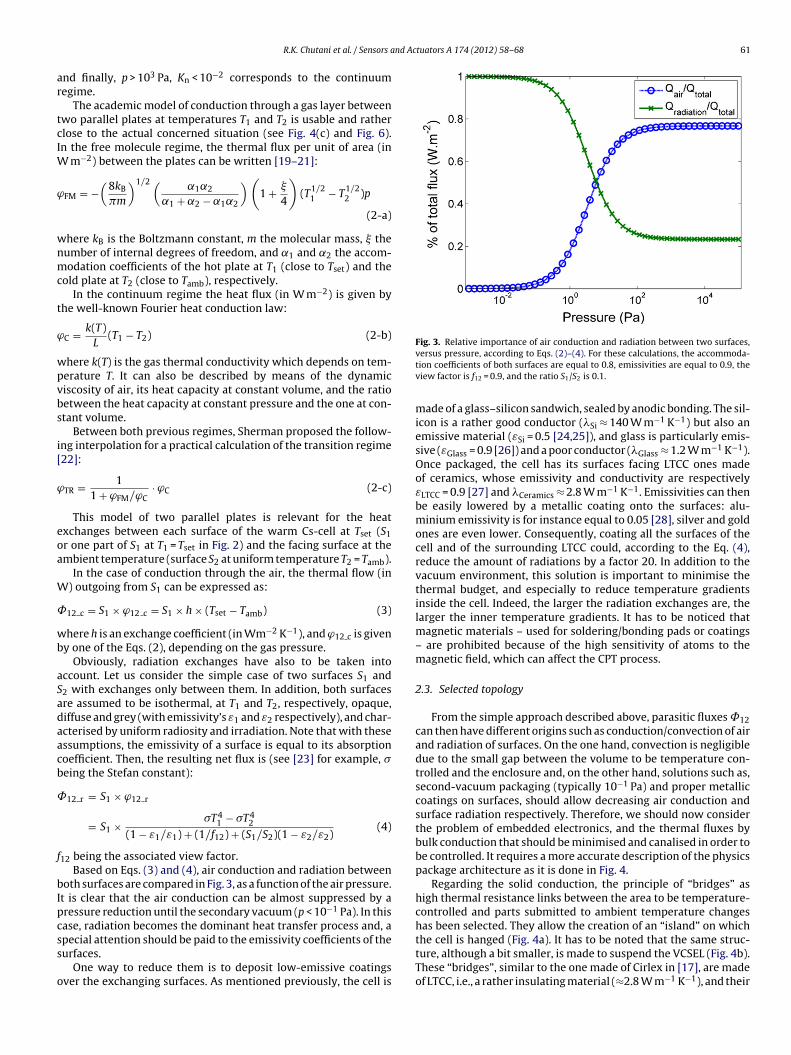
Fig. 3. Relative importance of air conduction and radiation between two surfaces,
R.K. Chutani et al. / Sensors a
nd finally, p > 103 Pa, Kn < 10−2 corresponds to the continuumegime.
The academic model of conduction through a gas layer betweenwo parallel plates at temperatures T1 and T2 is usable and ratherlose to the actual concerned situation (see Fig. 4(c) and Fig. 6).n the free molecule regime, the thermal flux per unit of area (in
m−2) between the plates can be written [19–21]:
FM = −(
8kB
�m
)1/2 (˛1˛2
˛1 + ˛2 − ˛1˛2
)(1 + �
4
)(T1/2
1 − T1/22 )p
(2-a)
here kB is the Boltzmann constant, m the molecular mass, � theumber of internal degrees of freedom, and ˛1 and ˛2 the accom-odation coefficients of the hot plate at T1 (close to Tset) and the
old plate at T2 (close to Tamb), respectively.In the continuum regime the heat flux (in W m−2) is given by
he well-known Fourier heat conduction law:
C = k(T)L
(T1 − T2) (2-b)
here k(T) is the gas thermal conductivity which depends on tem-erature T. It can also be described by means of the dynamiciscosity of air, its heat capacity at constant volume, and the ratioetween the heat capacity at constant pressure and the one at con-tant volume.
Between both previous regimes, Sherman proposed the follow-ng interpolation for a practical calculation of the transition regime22]:
TR = 11 + ϕFM/ϕC
· ϕC (2-c)
This model of two parallel plates is relevant for the heatxchanges between each surface of the warm Cs-cell at Tset (S1r one part of S1 at T1 = Tset in Fig. 2) and the facing surface at thembient temperature (surface S2 at uniform temperature T2 = Tamb).
In the case of conduction through the air, the thermal flow (in) outgoing from S1 can be expressed as:
12 c = S1 × ϕ12 c = S1 × h × (Tset − Tamb) (3)
here h is an exchange coefficient (in Wm−2 K−1), and ϕ12 c is giveny one of the Eqs. (2), depending on the gas pressure.
Obviously, radiation exchanges have also to be taken intoccount. Let us consider the simple case of two surfaces S1 and2 with exchanges only between them. In addition, both surfacesre assumed to be isothermal, at T1 and T2, respectively, opaque,iffuse and grey (with emissivity’s ε1 and ε2 respectively), and char-cterised by uniform radiosity and irradiation. Note that with thesessumptions, the emissivity of a surface is equal to its absorptionoefficient. Then, the resulting net flux is (see [23] for example, eing the Stefan constant):
12 r = S1 × ϕ12 r
= S1 × T41 − T4
2(1 − ε1/ε1) + (1/f12) + (S1/S2)(1 − ε2/ε2)
(4)
12 being the associated view factor.Based on Eqs. (3) and (4), air conduction and radiation between
oth surfaces are compared in Fig. 3, as a function of the air pressure.t is clear that the air conduction can be almost suppressed by aressure reduction until the secondary vacuum (p < 10−1 Pa). In thisase, radiation becomes the dominant heat transfer process and, a
pecial attention should be paid to the emissivity coefficients of theurfaces.One way to reduce them is to deposit low-emissive coatingsver the exchanging surfaces. As mentioned previously, the cell is
versus pressure, according to Eqs. (2)–(4). For these calculations, the accommoda-tion coefficients of both surfaces are equal to 0.8, emissivities are equal to 0.9, theview factor is f12 = 0.9, and the ratio S1/S2 is 0.1.
made of a glass–silicon sandwich, sealed by anodic bonding. The sil-icon is a rather good conductor (�Si ≈ 140 W m−1 K−1) but also anemissive material (εSi = 0.5 [24,25]), and glass is particularly emis-sive (εGlass = 0.9 [26]) and a poor conductor (�Glass ≈ 1.2 W m−1 K−1).Once packaged, the cell has its surfaces facing LTCC ones madeof ceramics, whose emissivity and conductivity are respectivelyεLTCC = 0.9 [27] and �Ceramics ≈ 2.8 W m−1 K−1. Emissivities can thenbe easily lowered by a metallic coating onto the surfaces: alu-minium emissivity is for instance equal to 0.05 [28], silver and goldones are even lower. Consequently, coating all the surfaces of thecell and of the surrounding LTCC could, according to the Eq. (4),reduce the amount of radiations by a factor 20. In addition to thevacuum environment, this solution is important to minimise thethermal budget, and especially to reduce temperature gradientsinside the cell. Indeed, the larger the radiation exchanges are, thelarger the inner temperature gradients. It has to be noticed thatmagnetic materials – used for soldering/bonding pads or coatings– are prohibited because of the high sensitivity of atoms to themagnetic field, which can affect the CPT process.
2.3. Selected topology
From the simple approach described above, parasitic fluxes ˚12can then have different origins such as conduction/convection of airand radiation of surfaces. On the one hand, convection is negligibledue to the small gap between the volume to be temperature con-trolled and the enclosure and, on the other hand, solutions such as,second-vacuum packaging (typically 10−1 Pa) and proper metalliccoatings on surfaces, should allow decreasing air conduction andsurface radiation respectively. Therefore, we should now considerthe problem of embedded electronics, and the thermal fluxes bybulk conduction that should be minimised and canalised in order tobe controlled. It requires a more accurate description of the physicspackage architecture as it is done in Fig. 4.
Regarding the solid conduction, the principle of “bridges” ashigh thermal resistance links between the area to be temperature-controlled and parts submitted to ambient temperature changeshas been selected. They allow the creation of an “island” on which
the cell is hanged (Fig. 4a). It has to be noted that the same struc-ture, although a bit smaller, is made to suspend the VCSEL (Fig. 4b).These “bridges”, similar to the one made of Cirlex in [17], are madeof LTCC, i.e., a rather insulating material (≈2.8 W m−1 K−1), and their
62 R.K. Chutani et al. / Sensors and Actuators A 174 (2012) 58– 68
F e mont e VCSEp re pac
dblath
giotVo
Fv
ig. 4. (a) Top view of demonstrated assembly that consists of 4 bridges and framemperature control. (b) Frames made of LTCC for hanging the cell (top frame) or thart is cell sub-system and lower part is VCSEL sub-system. All these components a
imensions can be easily calibrated. A resistance of 17 ◦C/mW perridge can then be achieved (bridges are about 0.5 mm width, 6 mm
ong, resistance calculation does not include the electrical leads). Inddition, only one temperature sensor is needed to control the areaemperature, since symmetries operate. This sensor, along with theeaters, is buried into the multi-layers LTCC material.
From the data and guidelines discussed above, various topolo-ies have been examined, e.g., a unique temperature-controllednsulated area supporting all the components (including some
f the dissipative electronics) such as in [15,16], or a uniqueemperature-controlled insulated area incorporating the cell,CSEL and the optics such as in [14,17] or only the cell [29]. Finally,ur selected solution (see Fig. 4c) consists of two insulated islands:ig. 5. (a) Resulting offsets of Cs-cell and VCSEL temperatures versus the ambient tempeersus ambient temperature, in steady state. This type of results shows that the heaters are
olithic system to support the Cs-cell. The same principle is applied for the VCSELL (bottom frame). (c) Sketch of the cross-section of demonstrator assembly; upperkaged in a multi-layers LTCC structure and encapsulated under vacuum.
one including the Cs-cell and the photodiode, and one correspond-ing to the VCSEL. Each block is separately temperature-controlled atits own set temperature. The optics sub-system (including neutraldensity, two lenses and a quarter-wave plate) is itself separatedfrom the VCSEL island. Thus, the suspensions support only theVCSEL or the cell. The power dissipated by the integrated electron-ics located near the VCSEL (about 15 mW), is directly evacuated tothe outside by conduction and does not heat the elements to betemperature-controlled. The enclosure surrounding the two LTCC
packages is under vacuum.In order to discriminate roughly the different topologies, simplecalculations based on the electrical analogy have been performed.This approach allows to easily consider the temperature-control
rature, in steady state, (b) main thermal fluxes involves in the analysed network, working all over the ambient temperature range, especially up to 55 ◦C if necessary.
R.K. Chutani et al. / Sensors and Actuators A 174 (2012) 58– 68 63
een v
fpg
tiiw
3m
dFstbdicctb
3
etLoa
eo(
f
o
ϕ
f
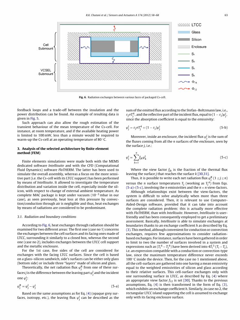
Fig. 6. Radiation exchanges betw
eedback loops and a trade-off between the insulation and theower distribution can be found. An example of resulting data isiven in Fig. 5.
Such approach can also allow the rough estimation of theransient behaviour of the mean temperature of the Cs-cell. Fornstance, at room temperature, and if the available heating powers limited to 100 mW, less than a minute would be required to
arm-up the Cs-cell at an operating temperature of 80 ◦C.
. Analysis of the selected architecture by finite elementethod (FEM)
Finite elements simulations were made both with the MEMSedicated software Intellisuite and with the CFD (Computationalluid Dynamics) software FloTHERM. The latter has been used toimulate the overall assembly, whereas a focus on the more sensi-ive part (i.e. the Cs-cell with its LTCC support) has been performedy means of Intellisuite. It allowed to investigate the temperatureistribution and variation inside the cell, especially inside the sil-
con, with respect to change of external ambient temperature. Asomplete MAC package is kept under vacuum (10−3 mbar in ourase), as seen previously, heat loss at this pressure by convec-ion/conduction through air is negligible and thus, heat exchangesy means of radiations are considered to be predominant.
.1. Radiation and boundary conditions
According to Fig. 6, heat exchanges through radiation should bexamined for two different areas: The first one (case no 1) concernshe exchanges between the cell surfaces and its facing ones made ofTCC, surrounding it similarly to a closed box, whereas the secondne (case no 2), includes exchanges between the LTCC cell supportnd the metallic enclosure.
For the 1st case, five sides of the cell are considered forxchanges with the facing LTCC surfaces. Since the cell is basedn a glass–silicon sandwich, side’s surfaces can be either only glassbottom side) or include three “layers” made of silicon and glass.
Theoretically, the net radiation flux ϕRj from one of these sur-
aces j is the difference between the leaving part ϕlj and the incident
ne ϕij:
Rj = ϕl
j − ϕij (5-a)
Based on the same assumptions as for Eq. (4) (opaque grey sur-aces, isotropy, etc.), the leaving flux ϕl
j can be described as the
arious faces of packaged Cs-cell.
sum of the emitted flux according to the Stefan–Boltzmann law, i.e.,εjT4
j , and the reflective part of the incident flux, equal to (1 − εj)ϕij,
since the absorption coefficient is equal to the emissivity:
ϕlj = εjT4
j + (1 − εj)ϕij (5-b)
Moreover, inside an enclosure, the incident flux ϕij is the sum of
the fluxes coming from all the n surfaces of the enclosure, seen bythe surface j, i.e.:
ϕij =
n∑k=1
fjkϕlk (5-c)
Where the view factor fjk is the fraction of the thermal fluxleaving the surface j that reaches the surface k [30,31].
Thus, it is possible to write each net radiation flux ϕRj (1 ≤ j ≤ n)
versus the n surface temperatures Tj (working as Tj4) from Eqs.
(5-a)–(5-c), involving the n emissivities and the n × n view-factors.Although relationships exist between the view-factors, the
system is difficult to solve analytically when more than threesurfaces are considered. Then, it is relevant to use Computer-Aided-Design software, provided that it can take into accountthe complete radiation problem: this is actually more effectivewith FloTHERM, than with Intellisuite. However, Intellisuite is user-friendly and has been consequently employed to get a preliminaryassessment. Basically, Intellisuite is able to simulate exchanges atboundaries thanks to an exchange coefficient h as described by Eq.(3). This method, although convenient for conduction or convectionexchanges, requires few approximations to consider radiation-based exchanges. For instance, surfaces have been gathered in orderto limit to two the number of surfaces involved in a system andexpressions such as (Ti
4 − Tj4) have been derived into 4Ti
3 (Ti − Tj),i.e. an expression compatible with a conduction or convection-typelaw, since the maximum temperature difference never exceeds100 ◦C inside the device. Then, for the case no 1 mentioned above,all the cell-surfaces are gathered into one having a mean emissivityequal to the weighted emissivities of silicon and glass accordingto their relative surfaces. This cell-surface exchanges only withone surrounding surface in LTCC, as described by Eq. (4) wherean appropriate view factor f12 is set [30]. Thanks to the previous
assumptions, Eq. (4) is then transformed in the form of Eq. (3),which exhibits an exchange coefficient h. Similarly, in case no 2, therectangular LTCC island supporting the cell is assumed to exchangeonly with its facing enclosure surface.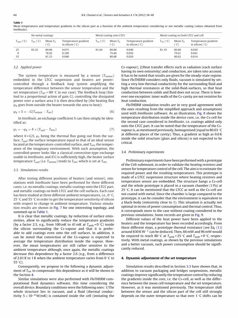
64 R.K. Chutani et al. / Sensors and Actuators A 174 (2012) 58– 68
Table 1Mean temperatures and temperature gradients in the silicon part as a function of the ambient temperature considering or not metallic coating (values obtained fromIntellisuite).
No metal coatings Metal coating onto LTCC Metal coating on both LTCC and cell
Tamb (◦C) Tset (◦C) Mean TSi
(◦C)Temperature gradientin silicon (◦C)
Tset (◦C) Mean TSi
(◦C)Temperature gradientin silicon (◦C)
Tset (◦C) Mean TSi
(◦C)Temperature gradientin silicon (◦C)
0
6
8
3
ectsipϕ
ϕ
t
ϕ
wflacut
3
ucah2wts
s(tacaeado5
mt
powt
25 83.32 80.00 0.075 81.64 80.00 78.92 0.100 79.4
55 81.53 0.040 80.8
.2. Applied power
The system temperature is measured by a sensor (Tsensor)mbedded in the LTCC suspension and heaters are power-ontrolled through a feedback loop system amplifying theemperature difference between the sensor temperature and theet temperature (Tset ≈ 80 ◦C in our case). The feedback loop (lim-ted to a proportional action of gain G), controlling the dissipatedower over a surface area S is then described by (the heating fluxh goes from outside the heater towards the area to heat):
h × S = −G(Tsensor − Tset) (6)
In Intellisuit, an exchange coefficient h can then simply be iden-ified as:
s = −ϕh = h × (Tsurf − Tenv) (7)
here h = G/S, ϕs being the thermal flux going out from the sur-ace, Tsurf the surface temperature equal to that of an ideal sensorocated at the temperature-controlled surface, and Tenv the temper-ture of the imaginary environment. With such assumption, theontrolled-power looks like a classical convection-type exchangesable in Intellisuite, and if G is sufficiently high, the heater surfaceemperature Tsurf (i.e. Tsensor) tends to Tenv which is set at Tset.
.3. Simulations results
After testing different positions of heaters (and sensor), sim-lations with Intellisuite have been performed for three differentases; i.e. no metallic coatings, metallic coatings onto the LTCC part,nd metallic coatings on both LTCC and the cell surfaces. Each caseas been studied at three different ambient temperatures, i.e., 0 ◦C,5 ◦C and 55 ◦C in order to get the temperature sensitivity of siliconith respect to change in ambient temperature. Various simula-
ion results are shown in Fig. 7 for one interesting topology, andummed-up in Table 1.
It is clear that metallic coatings, by reduction of surface emis-ivities, allow to significantly reduce the temperature gradientsby a factor 2.5, e.g., from 100 mK to 41 mK at Tamb = 0 ◦C) insidehe silicon surrounding the Cs-vapour and that it is prefer-ble to add coatings even onto the cell surfaces. In addition, itan be noted that convection of the Cs-vapour is expected toverage the temperature distribution inside the vapour. How-ver, the mean temperatures are still rather sensitive to thembient temperature although, once again, the metallic coatingsecrease this dependence by a factor 2.6 (e.g., from a differencef 2.61 K to 1 K when the ambient temperature varies from 0 ◦C to5 ◦C).
Consequently, we propose in the following a dynamic adjust-ent of Tset to compensate this dependence as it will be shown in
he Section 4.Similar simulations were also performed with FloTHERM com-
utational fluid dynamics software, this time considering theverall device. Boundary conditions were the following ones: 1/Thehole structure lies in vacuum, and a fluid (thermal conduc-
ivity 5 × 10⁻⁴ W/mK) is contained inside the cell (imitating the
0.040 81.10 80.00 0.0300.056 79.61 0.0410.020 80.62 0.014
Cs-vapour), 2/Heat transfer effects such as radiation (each surfacehaving its own emissivity) and conduction, are taken into account.It has to be noted that results are given for the steady-state regime.Since FloTHERM considers only fluids, vacuum is simulated by set-ting a very low thermal conductivity for the surrounding fluid andhigh thermal resistances at the solid-fluid-surfaces, so that heatconduction between solids and fluid does not occur. There is how-ever one exception: inner walls of the Cs-cavity are not resistive forheat conduction.
FloTHERM simulation results are in very good agreement withthe ones resulting from the simplified approach and assumptionsused with Intellisuite software. As an illustration, Fig. 8 shows thetemperature distribution inside the device core, i.e. the Cs-cell forthe second case considered in Intellisuite, i.e. coatings added onlyonto the LTCC part. It can be noted that the temperature of the Cs-vapour is, as mentioned previously, homogenised (equal to 80.03 ◦Cat different places of the cavity). Thus, a gradient as high as 0.6 Kinside the solid structure (glass and silicon) is not expected to becritical.
3.4. Preliminary experiments
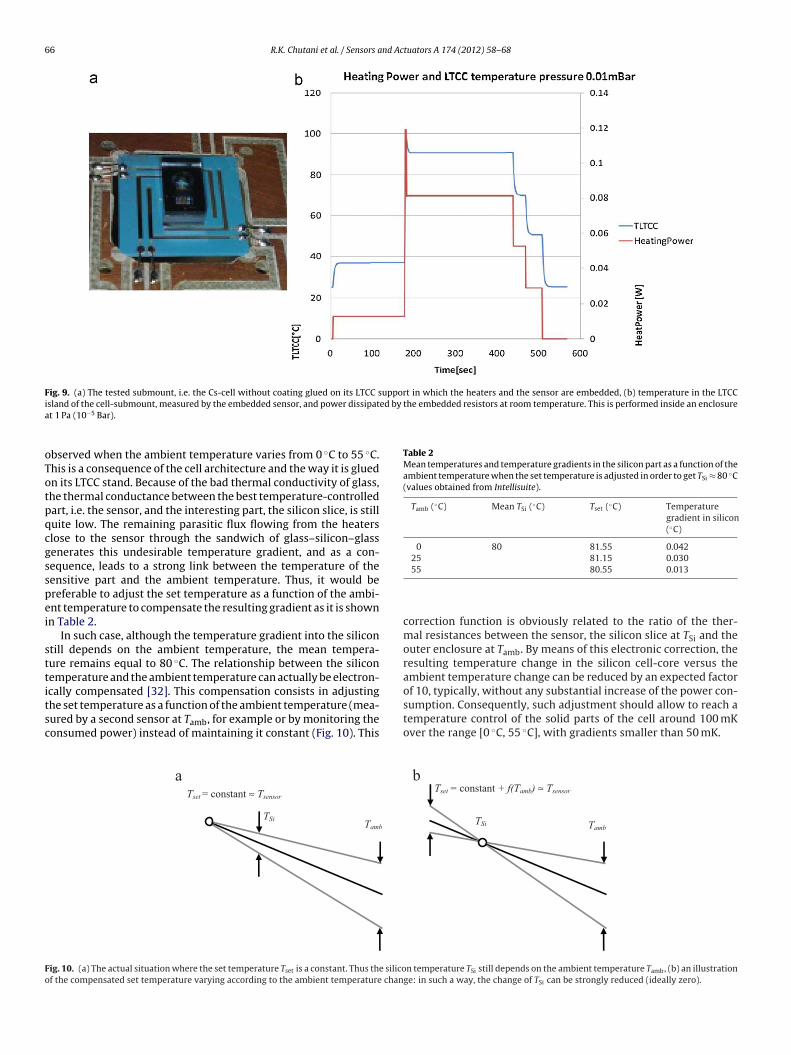
Preliminary experiments have been performed with a prototypeof the Cell-submount, in order to validate the heating resistors andsensor for temperature control of the cell. The aim is to estimate therequired power and the resulting temperatures. This prototype ismade of a LTCC suspension structure where heating resistors andtemperature sensor are embedded. The structure hangs a Cs-celland the whole prototype is placed in a vacuum chamber (1 Pa) at25 ◦C. It can be mentioned that the LTCC as well as the Cs-cell arenot coated with metal. Since the chamber is large compared to theprototype, it can be consider that the environment is equivalent toa black-body (emissivity close to 1). This situation is actually notoptimal in terms of power consumption and thermal control. Thus,it corresponds more to the case without coating considered in theprevious simulations. Some records are given in Fig. 9.
Different values of the heat power have been applied to theheaters and the temperature has been recorded accordingly. Fromthese different steps, a prototype thermal resistance (see Eq. (1))around 830 K W−1 can be deduced. Then, 66 mW and 96 mW wouldbe required to reach 80 ◦C at Tamb = 25 ◦C and Tamb = 0 ◦C, respec-tively. With metal coatings, as shown by the previous simulationsand a better vacuum, such power consumption should be signifi-cantly reduced.
4. Dynamic adjustment of the set temperature
Simulation results described in Section 3.3 have shown that, inaddition to vacuum packaging and bridges suspensions, metalliccoatings improve significantly the temperature control by reducingthe gradients inside the core, i.e. the Cs-cell, as well as the differ-
ence between the mean cell temperature and the set temperature.However, as it was mentioned previously. The temperature shiftbetween the sensor and the silicon part of the cell still stronglydepends on the outer temperature so that over 1 ◦C shifts can be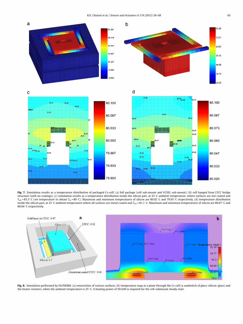
R.K. Chutani et al. / Sensors and Actuators A 174 (2012) 58– 68 65
Fig. 7. Simulation results as a temperature distribution of packaged Cs-cell; (a) full package (cell sub-mount and VCSEL sub-mount), (b) cell hanged from LTCC bridgestructure (with no coatings), (c) simulation results as a temperature distribution inside the silicon part, at 25 ◦C ambient temperature, where surfaces are not coated andTset = 83.3 ◦C (set temperature to obtain TSi = 80 ◦C). Maximum and minimum temperatures of silicon are 80.02 ◦C and 79.95 ◦C respectively, (d) temperature distributioninside the silicon part, at 25 ◦C ambient temperature where all surfaces are metal coated and Tset = 81.1 ◦C. Maximum and minimum temperatures of silicon are 80.07 ◦C and80.04 ◦C respectively.
Fig. 8. Simulation performed by FloTHERM; (a) emissivities of various surfaces, (b) temperature map at a plane through the Cs-cell (a sandwitch of glass–silicon–glass) andthe heater resistors, when the ambiant temperature is 25 ◦C. A heating power of 50 mW is required for the cell-submount steady state.
66 R.K. Chutani et al. / Sensors and Actuators A 174 (2012) 58– 68
Fig. 9. (a) The tested submount, i.e. the Cs-cell without coating glued on its LTCC support in which the heaters and the sensor are embedded, (b) temperature in the LTCCi ed by the embedded resistors at room temperature. This is performed inside an enclosurea
oTotpqcgsspei
sttitsc
Table 2Mean temperatures and temperature gradients in the silicon part as a function of theambient temperature when the set temperature is adjusted in order to get TSi ≈ 80 ◦C(values obtained from Intellisuite).
Tamb (◦C) Mean TSi (◦C) Tset (◦C) Temperaturegradient in silicon(◦C)
0 80 81.55 0.04225 81.15 0.030
Fo
sland of the cell-submount, measured by the embedded sensor, and power dissipatt 1 Pa (10−5 Bar).
bserved when the ambient temperature varies from 0 ◦C to 55 ◦C.his is a consequence of the cell architecture and the way it is gluedn its LTCC stand. Because of the bad thermal conductivity of glass,he thermal conductance between the best temperature-controlledart, i.e. the sensor, and the interesting part, the silicon slice, is stilluite low. The remaining parasitic flux flowing from the heaterslose to the sensor through the sandwich of glass–silicon–glassenerates this undesirable temperature gradient, and as a con-equence, leads to a strong link between the temperature of theensitive part and the ambient temperature. Thus, it would bereferable to adjust the set temperature as a function of the ambi-nt temperature to compensate the resulting gradient as it is shownn Table 2.
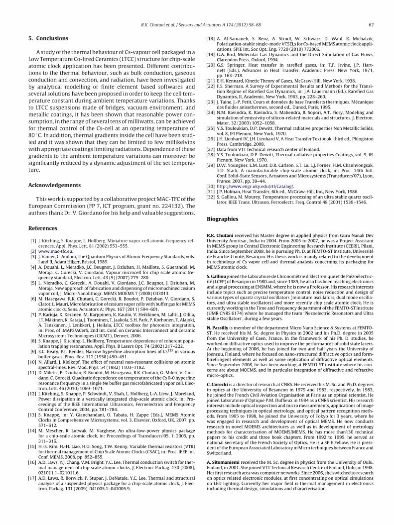
In such case, although the temperature gradient into the silicontill depends on the ambient temperature, the mean tempera-ure remains equal to 80 ◦C. The relationship between the siliconemperature and the ambient temperature can actually be electron-
cally compensated [32]. This compensation consists in adjustinghe set temperature as a function of the ambient temperature (mea-ured by a second sensor at Tamb, for example or by monitoring theonsumed power) instead of maintaining it constant (Fig. 10). ThisTset = cons tan t ≈ Tsensor
TSi Tamb
a
ig. 10. (a) The actual situation where the set temperature Tset is a constant. Thus the silicof the compensated set temperature varying according to the ambient temperature chan
55 80.55 0.013
correction function is obviously related to the ratio of the ther-mal resistances between the sensor, the silicon slice at TSi and theouter enclosure at Tamb. By means of this electronic correction, theresulting temperature change in the silicon cell-core versus theambient temperature change can be reduced by an expected factorof 10, typically, without any substantial increase of the power con-
sumption. Consequently, such adjustment should allow to reach atemperature control of the solid parts of the cell around 100 mKover the range [0 ◦C, 55 ◦C], with gradients smaller than 50 mK.TambTSi
Tset = cons tant + f(Tamb) ≈ Tsensor
b
n temperature TSi still depends on the ambient temperature Tamb, (b) an illustrationge: in such a way, the change of TSi can be strongly reduced (ideally zero).
nd Ac
5
Latcbsptmsf8iwgst
A
Ea
R
[
[
[
[
[
[
[
[
[
[
[
[[
[
[
[
[
[[
[
[[[
R.K. Chutani et al. / Sensors a
. Conclusions
A study of the thermal behaviour of Cs-vapour cell packaged in aow Temperature Co-fired Ceramics (LTCC) structure for chip-scaletomic clock application has been presented. Different contribu-ions to the thermal behaviour, such as bulk conduction, gaseousonduction and convection, and radiation, have been investigatedy analytical modelling or finite element based softwares andeveral solutions have been proposed in order to keep the cell tem-erature constant during ambient temperature variations. Thankso LTCC suspensions made of bridges, vacuum environment, and
etallic coatings, it has been shown that reasonable power con-umption, in the range of several tens of milliwatts, can be achievedor thermal control of the Cs-cell at an operating temperature of0 ◦C. In addition, thermal gradients inside the cell have been stud-
ed and it was shown that they can be limited to few millikelvinsith appropriate coatings limiting radiations. Dependence of these
radients to the ambient temperature variations can moreover beignificantly reduced by a dynamic adjustment of the set tempera-ure.
cknowledgements
This work is supported by a collaborative project MAC-TFC of theuropean Commission (FP 7, ICT program, grant no. 224132). Theuthors thank Dr. V. Giordano for his help and valuable suggestions.
eferences
[1] J. Kitching, S. Knappe, L. Hollberg, Miniature vapor-cell atomic-frequency ref-erences, Appl. Phys. Lett. 81 (2002) 553–555.
[2] www.mac-tfc.eu.[3] J. Vanier, C. Audoin, The Quantum Physics of Atomic Frequency Standards, vols.
I and II, Adam Hilger, Bristol, 1989.[4] A. Douahi, L. Nieradko, J.C. Beugnot, J. Dziuban, H. Maillote, S. Guerandel, M.
Moraja, C. Gorecki, V. Giordano, Vapour microcell for chip scale atomic fre-quency standard, Electron. Lett. 43 (5) (2007) 279–280.
[5] L. Nieradko, C. Gorecki, A. Douahi, V. Giordano, J.C. Beugnot, J. Dziuban, M.Moraja, New approach of fabrication and dispensing of micromachined cesiumvapor cell, J. Micro-Nanolithogr. MEMS MOEMS 7 (2008) 033013.
[6] M. Hasegawa, R.K. Chutani, C. Gorecki, R. Boudot, P. Dziuban, V. Giordano, S.Clatot, L. Mauri, Microfabrication of cesium vapor cells with buffer gas for MEMSatomic clocks, Sens. Actuators A: Phys. 167 (2011) 594–601.
[7] P. Karioja, K. Keränen, M. Karppinen, K. Kautio, V. Heikkinen, M. Lahti, J. Ollila,J.T. Mäkinen, K. Kataja, J. Tuominen, T. Jaakola, S.H. Park, P. Korhonen, T. Alajoki,A. Tanskanen, J. Lenkkeri, J. Heilala, LTCC toolbox for photonics integration,in: Proc. of IMAPS/ACerS, 2nd Int. Conf. on Ceramic Interconnect and CeramicMicrosystems Technologies (CICMT), Denver, 2006.
[8] S. Knappe, J. Kitching, L. Hollberg, Temperature dependence of coherent popu-lation trapping resonances, Appl. Phys. B Lasers Opt. 74 (2002) 217–222.
[9] E.C. Beaty, P.L. Bender, Narrow hyperfine absorption lines of Cs133 in variousbuffer gases, Phys. Rev. 112 (1958) 450–451.
10] N. Allard, J. Kielkopf, The effect of neutral non-resonant collisions on atomicspectral-lines, Rev. Mod. Phys. 54 (1982) 1103–1182.
11] D. Miletic, P. Dziuban, R. Boudot, M. Hasegawa, R.K. Chutani, G. Mileti, V. Gior-dano, C. Gorecki, Quadratic dependence on temperature of the Cs 0-0 hyperfineresonance frequency in a single Ne buffer gas microfabricated vapor cell, Elec-tron. Lett. 46 (2010) 1069–1071.
12] J. Kitching, S. Knappe, P. Schwindt, V. Shah, L. Hollberg, L-A. Liew, J. Moreland,Power dissipation in a vertically integrated chip-scale atomic clock, in: Pro-ceedings of the IEEE International Ultrasonics, Ferroelectrics and FrequencyControl Conference, 2004, pp. 781–784.
13] S. Knappe, in: Y. Gianchandani, O. Tabata, H. Zappe (Eds.), MEMS AtomicClocks in Comprehensive Microsystems, vol. 3, Elsevier, Oxford, UK, 2007, pp.571–612.
14] M. Mescher, R. Lutwak, M. Varghese, An ultra-low-power physics packagefor a chip-scale atomic clock, in: Proceedings of Transducers’05, 1, 2005, pp.311–316.
15] H.-S. Kim, H.-H. Liao, H.O. Song, T.W. Kenny, Variable thermal resistors (VTR)for thermal management of Chip Scale Atomic Clocks (CSAC), in: Proc. IEEE Int.Conf. MEMS, 2008, pp. 852–855.
16] A.D. Laws, Y.J. Chang, V.M. Bright, Y.C. Lee, Thermal conduction switch for ther-
mal management of chip scale atomic clocks, J. Electron. Packag. 130 (2008),021011.1–021011.6.17] A.D. Laws, R. Borwick, P. Stupar, J. DeNatale, Y.C. Lee, Thermal and structuralanalysis of a suspended physics package for a chip-scale atomic clock, J. Elec-tron. Packag. 131 (2009), 041005.1–041005.9.
tuators A 174 (2012) 58– 68 67
18] A. Al-Samaneh, S. Renz, A. Strodl, W. Schwarz, D. Wahl, R. Michalzik,Polarization-stable single-mode VCSELs for Cs-based MEMS atomic clock appli-cations, SPIE Int. Soc Opt. Eng. 7720 (2010) 772006.
19] G.A. Bird, Molecular Gas Dynamics and the Direct Simulation of Gas Flows,Clarendon Press, Oxford, 1994.
20] G.S. Springer, Heat transfer in rarefied gases, in: T.F. Irvine, J.P. Hart-nett (Eds.), Advances in Heat Transfer, Academic Press, New York, 1971,pp. 163–218.
21] E.H. Kennard, Kinetic Theory of Gases, McGraw-Hill, New York, 1938.22] F.S. Sherman, A Survey of Experimental Results and Methods for the Transi-
tion Regime of Rarefied Gas Dynamics, in: J.A. Lauermann (Ed.), Rarefied GasDynamics, II, Academic, New York, 1963, pp. 228–260.
23] J. Taine, J.-P. Petit, Cours et données de base Transferts thermiques. Mécaniquedes fluides anisothermes, second ed., Dunod, Paris, 1995.
24] N.M. Ravindra, K. Ravindra, S. Mahendra, B. Sopori, A.T. Fiory, Modeling andsimulation of emissivity of silicon-related materials and structures, J. Electron.Mater. 32 (2003) 1052–1058.
25] Y.S. Touloukian, D.P. Dewitt, Thermal radiative properties Non Metallic Solids,vol. 8, IFI Plenum, New York, 1970.
26] J.H. Lienhard IV, J.H. Lienhard V, A Heat Transfer Textbook, third ed., PhlogistonPress, Cambridge, 2008.
27] Data from VTT technical research center of Finland.28] Y.S. Touloukian, D.P. Dewitt, Thermal radiative properties Coatings, vol. 9, IFI
Plenum, New York, 1970.29] D.W. Youngner, L.M. Lust, D.R. Carlson, S.T. Lu, L.J. Forner, H.M. Chanhvongsak,
T.D. Stark, A manufacturable chip-scale atomic clock, in: Proc. 14th Intl.Conf. Solid-State Sensors, Actuators and Microsystems (Transducers’07), Lyon,France, 2007, pp. 39–44.
30] http://www.engr.uky.edu/rtl/Catalog/.31] J.P. Holman, Heat Transfer, 6th ed., McGraw-Hill, Inc., New York, 1986.32] S. Galliou, M. Mourey, Temperature processing of an ultra stable quartz oscil-
lator, IEEE Trans. Ultrason. Ferroelectr. Freq. Control 48 (2001) 1539–1546.
Biographies
R.K. Chutani received his Master degree in applied physics from Guru Nanak DevUniversity Amritsar, India in 2004. From 2005 to 2007, he was a Project Assistantin MEMS group in Central Electronic Engineering Research Institute (CEERI), Pilani,India. Since September 2008, he is pursuing Ph. D. at FEMTO-ST Institute, Universitéde Franche-Comté, Besanc on. His thesis work is mainly related to the developmentin technology of Cs vapor cell and thermal analysis concerning its packaging forMEMS atomic clock.
S. Galliou joined the Laboratoire de Chronométrie d’Electronique et de Piézoélectric-ité (LCEP) of Besanc on in 1980 and, since 1985, he also has been teaching electronicsand signal processing at ENSMM, where he is now a Professor. His research interestsinclude topics such as precise temperature control, noise reduction and design ofvarious types of quartz crystal oscillators (miniature oscillators, dual mode oscilla-tors, and ultra stable oscillators) and more recently chip scale atomic clock. He iscurrently working in the Time and Frequency department of the FEMTO-ST Institute(UMR CNRS 6174) where he managed the team ‘Piezoelectric Resonators and Ultrastable Oscillators’, during a few years.
N. Passilly is member of the department Micro Nano Science & Systems at FEMTO-ST. He received his M. Sc. degree in Physics in 2002 and his Ph.D. degree in 2005from the University of Caen, France. In the framework of his Ph. D. studies, heworked on diffractive optics used to improve the performances of solid state lasers.At the beginning of 2006, he has joined for two and half years the University ofJoensuu, Finland, where he focused on nano-structured diffractive optics and form-birefringent elements as well as some replication of diffractive optical elements.Since September 2008, he has been working at FEMTO-ST institute where his con-cerns are about MOEMS, and in particular integration of diffractive and refractivemicro-optics.
C. Gorecki is a director of research at CNRS. He received his M. Sc. and Ph.D. degreesin optics at the University of Besancon in 1979 and 1983, respectively. In 1983,he joined the French Civil Aviation Organisation at Paris as an optical scientist. Hejoined Laboratoire d’Optique P.M. Duffieux in 1984 as a CNRS scientist. His researchinterests include optical inspection and micro measurements, applications of imageprocessing techniques in optical metrology, and optical pattern recognition meth-ods. From 1995 to 1998, he joined the University of Tokyo for 3 years, where hewas engaged in research and development of optical MEMS. He now conductsresearch in novel MOEMS architectures as well as in development of metrologymethods for characterisation of MOEMS/MEMS. He has more than130 technicalpapers to his credit and three book chapters. From 1992 to 1995, he served asnational secretary of the French Society of Optics. He is a SPIE Fellow. He is presi-dent of the European Associated Laboratory in Micro techniques between France andSwitzerland.
A. Sitomaniemi received the M. Sc. degree in physics from the University of Oulu,
Finland, in 2001. She joined VTT Technical Research Centre of Finland, Oulu, in 1998.Her first research area was computer networks. Since 2006, she switched to researchon optics related electronic modules, at first concentrating on optical simulationson LED lighting. Currently her major field is thermal management in electronicsincluding thermal design, simulations and characterisation.
6 nd Ac
MFi
KsRaMMi
As
In the 1990, he joined the Neuchâtel Observatory as project leader and worked onlaser diodes stabilisation on atomic lines (Rb), and development of atomic clocks(hydrogen masers for ground and space applications). Since 2006 he is working
8 R.K. Chutani et al. / Sensors a
. Heikkinen received the M. Sc. degree in electronics from the University of Oulu,inland, in 1996. Presently, he is Chief Engineer at Tactotek Ltd, Finland his researchnterest is Hybrid integration of optical touch panels.
. Kautio received the M. Sc. degree in electrical engineering from Oulu Univer-ity, Oulu, Finland in 1983. In 1989, he joined VTT, where he is working as a Senioresearch Scientist on LTCC processing technology and ceramic based module pack-ging. From 1987 to 1989, he worked as a Thick Film Process Engineer at Aspoicroelectronics. From 1983 to 1987, he was a Research Scientist at Oulu University
icroelectronics laboratory, working on thick film hybrid applications. Mr. Kautios a member of IMAPS.
. Keränen received his Ph.D. degree in 2003 in theoretical physics from the Univer-ity of Oulu, Finland. Presently, he working as Chief Technology Officer at TactoTek
tuators A 174 (2012) 58– 68
Ltd, Finland and his research Interest includes optical touch panels and other sensingsolutions.
A. Jornod Born in 1957. He is Physicist, and pursued his diploma from the Universityof Neuchâtel, Switzerland (1982). From 1984 to 1990, he worked as project leaderat CSEM and his work was related to the development of silicon mechanical sensors.
as project leader in the development of sensor systems for watch applications atSwatch Group R&D Ltd, Division ASULAB.


