Embed Size (px)
Citation preview
RF MEMS and MEMS Packaging Motoaki Hara and Masayoshi Esashi*
Graduate School of Engineering, Tohoku University
*New Industry Hatchery Center (NICHe), Tohoku University 01 Aoba, Aramaki-aza, Aoba-ku, Sendai 980-8579, Japan
Tel.: +81-22-217-6937, Fax.: +81-22-217-6935
Abstract — A wafer level MEMS encapsulation and an array MEMS - IC assembly using a glass with high density electrical feed-through are described as MEMS packaging techniques. An accelerometer, a multi-column electron beam lithography system and a multi probe data storage are described as the packaged MEMS devices. A thermal MEMS switch using the wafer level MEMS encapsulation and an AlN based FBAR (thin film bulk acoustic resonator) are described as RF MEMS devices.
Index Terms — MEMS, packaging, feed-through, RF switch and FBAR.
I. INTRODUCTION
Sealing to protect MEMS devices from an external environment is needed in practical use of MEMS (micro electro mechanical systems) and NEMS (nano electro mechanical systems) devices. Furthermore, in array MEMS such as multi probe data storage, inteconnection using high density electrical feed-through from the array MEMS to the control IC is required.
In order to facilitate anodic bonding for these purposes, the glass with electrical feed-through has been developed. and concepts of the packagings of MEMS devices using this glass have been proposed. The glass feed-through and its applications will be described below.
RF MEMS is one of the most exiting fields of MEMS research area owing to the enormous market of the wireless communications. Mechanical switches, variable capacitors, mechanical resonators, suspended planer inductors and many attractive devices have been reported.
A thermal MEMS switch and an air gap type FBAR (thin film bulk acoustic resonator) will be also described.
II. PACKAGING TECHNIQUES USING GLASS WITH ELECTRICAL FEED-THROUGH
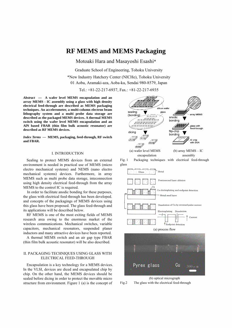
Encapsulation is a key technology for a MEMS devices. In the VLSI, devices are diced and encapsulated chip by chip. On the other hand, the MEMS devices should be sealed before dicing in order to protect the movable micro structure from environment. Figure 1 (a) is the concept of
(a) wafer level MEMS (b) array MEMS – IC encapsulation assembly
Fig. 1 Packaging techniques with electrical feed-through glass
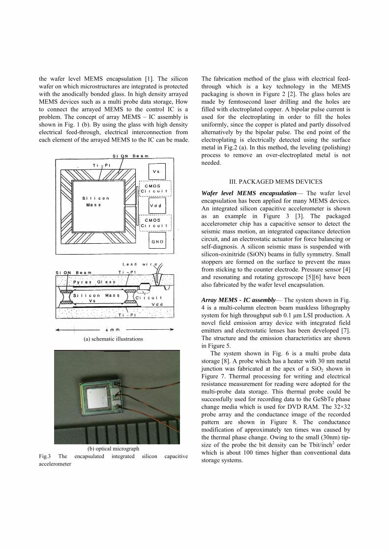
(a) process flow
(b) optical micrograph Fig.2 The glass with the electrical feed-through
the wafer level MEMS encapsulation [1]. The silicon wafer on which microstructures are integrated is protected with the anodically bonded glass. In high density arrayed MEMS devices such as a multi probe data storage, How to connect the arrayed MEMS to the control IC is a problem. The concept of array MEMS – IC assembly is shown in Fig. 1 (b). By using the glass with high density electrical feed-through, electrical interconnection from each element of the arrayed MEMS to the IC can be made.
(a) schematic illustrations
(b) optical micrograph Fig.3 The encapsulated integrated silicon capacitive accelerometer
The fabrication method of the glass with electrical feed-through which is a key technology in the MEMS packaging is shown in Figure 2 [2]. The glass holes are made by femtosecond laser drilling and the holes are filled with electroplated copper. A bipolar pulse current is used for the electroplating in order to fill the holes uniformly, since the copper is plated and partly dissolved alternatively by the bipolar pulse. The end point of the electroplating is electrically detected using the surface metal in Fig.2 (a). In this method, the leveling (polishing) process to remove an over-electroplated metal is not needed.
III. PACKAGED MEMS DEVICES
Wafer level MEMS encapsulation— The wafer level encapsulation has been applied for many MEMS devices. An integrated silicon capacitive accelerometer is shown as an example in Figure 3 [3]. The packaged accelerometer chip has a capacitive sensor to detect the seismic mass motion, an integrated capacitance detection circuit, and an electrostatic actuator for force balancing or self-diagnosis. A silicon seismic mass is suspended with silicon-oxinitride (SiON) beams in fully symmetry. Small stoppers are formed on the surface to prevent the mass from sticking to the counter electrode. Pressure sensor [4] and resonating and rotating gyroscope [5][6] have been also fabricated by the wafer level encapsulation. Array MEMS - IC assembly— The system shown in Fig. 4 is a multi-column electron beam maskless lithography system for high throughput sub 0.1 µm LSI production. A novel field emission array device with integrated field emitters and electrostatic lenses has been developed [7]. The structure and the emission characteristics are shown in Figure 5.
The system shown in Fig. 6 is a multi probe data storage [8]. A probe which has a heater with 30 nm metal junction was fabricated at the apex of a SiO2 shown in Figure 7. Thermal processing for writing and electrical resistance measurement for reading were adopted for the multi-probe data storage. This thermal probe could be successfully used for recording data to the GeSbTe phase change media which is used for DVD RAM. The 32×32 probe array and the conductance image of the recorded pattern are shown in Figure 8. The conductance modification of approximately ten times was caused by the thermal phase change. Owing to the small (30nm) tip-size of the probe the bit density can be Tbit/inch2 order which is about 100 times higher than conventional data storage systems.
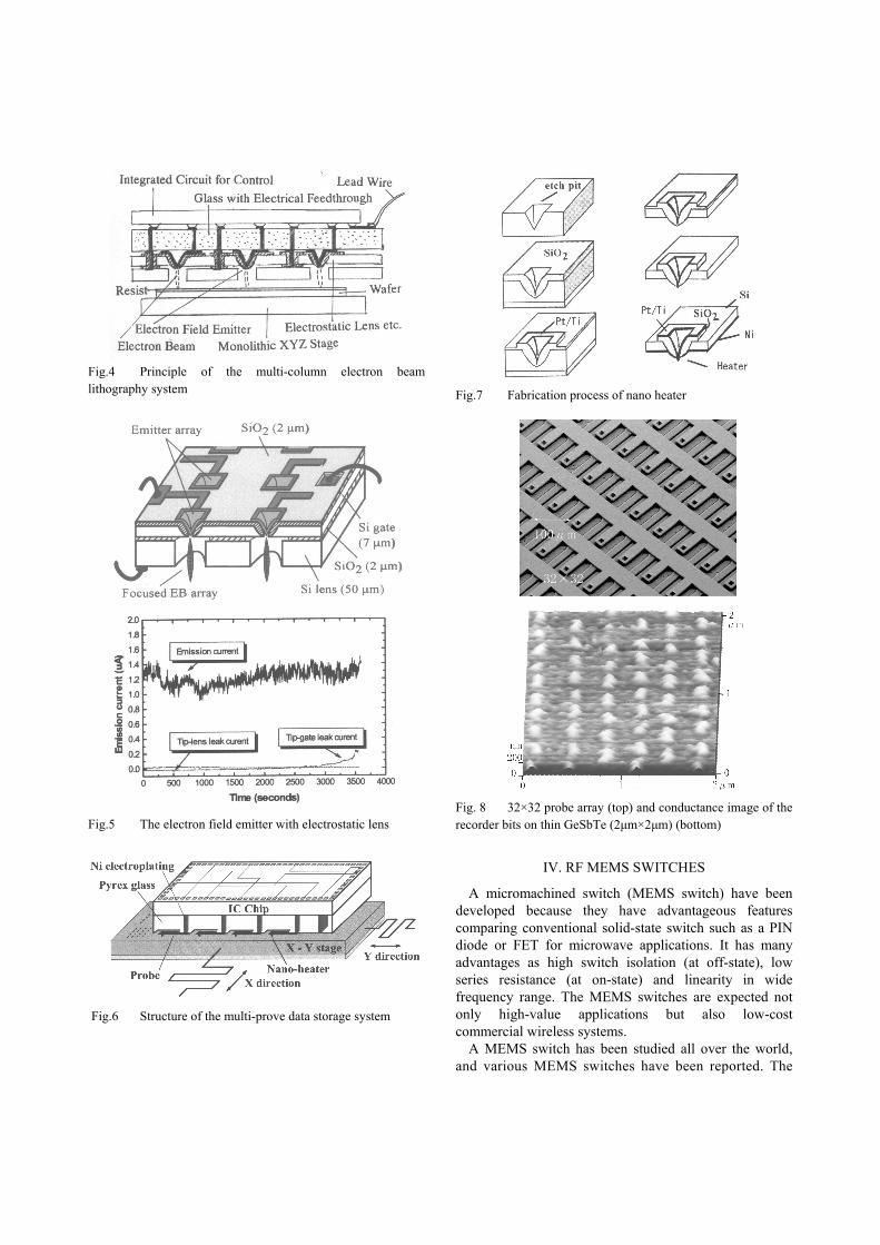
Fig.4 Principle of the multi-column electron beam lithography system
Fig.5 The electron field emitter with electrostatic lens
Fig.6 Structure of the multi-prove data storage system
Fig.7 Fabrication process of nano heater
Fig. 8 32×32 probe array (top) and conductance image of the recorder bits on thin GeSbTe (2µm×2µm) (bottom)
IV. RF MEMS SWITCHES
A micromachined switch (MEMS switch) have been developed because they have advantageous features comparing conventional solid-state switch such as a PIN diode or FET for microwave applications. It has many advantages as high switch isolation (at off-state), low series resistance (at on-state) and linearity in wide frequency range. The MEMS switches are expected not only high-value applications but also low-cost commercial wireless systems.
A MEMS switch has been studied all over the world, and various MEMS switches have been reported. The
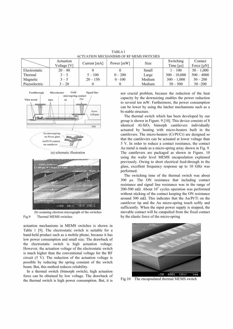
TABLA I
ACTUATION MECHANISMS OF RF MEMS SWITCHES Actuation
Voltage [V] Current [mA] Power [mW] Size Switching Time [µs]
Contact Force [µN]
Electrostatic Thermal Magnetic Piezoelectric
20 – 80 3 – 5 3 – 5 3 – 20
0 5 – 100
20 – 150 0
0 0 – 200 0 –100
0
Small Large
Medium Medium
1 – 100 300 – 10,000 300 – 1,000
50 – 500
50 – 1,000500 – 4000
50 – 200 50 –200
(a) schematic illustration
(b) scanning electron micrograph of the switches Fig.9 Thermal MEMS switches actuation mechanisms in MEMS switches is shown in Table 1 [9]. The electrostatic switch is suitable for a hand-held product such as a mobile phone, because it has low power consumption and small size. The drawback of the electrostatic switch is high actuation voltage. However, the actuation voltage of the electrostatic switch is much higher than the conventional voltage for the RF circuit (5 V). The reduction of the actuation voltage is possible by reducing the spring constant of the switch beam. But, this method reduces reliability.
In a thermal switch (bimorph switch), high actuation force can be obtained by low voltage. The drawback of the thermal switch is high power consumption. But, it is
not crucial problem, because the reduction of the heat capacity by the downsizing enables the power reduction to several ten mW. Furthermore, the power consumption can be lower by using the latchet mechanisms such as a bi-stable structure.
The thermal switch which has been developed by our group is shown in Figure. 9 [10]. This device consists of 8 identical Al-SiO2 bimorph cantilevers individually actuated by heating with micro-heaters built in the cantilevers. The micro-heaters (Cr/Pt/Cr) are designed so that the cantilevers can be actuated at lower voltage than 5 V. In order to reduce a contact resistance, the contact Au metal is made as a micro-spring array shown in Fig. 9. The cantilevers are packaged as shown in Figure. 10 using the wafer level MEMS encapsulation explained previously. Owing to short electrical feed-through in the glass, excellent frequency response up to 10 GHz was performed.
The switching time of the thermal switch was about 300 µs. The ON resistance that including contact resistance and signal line resistance was in the range of 200-500 mΩ. About 107 cycles operation was performed without sticking of the contact keeping the ON resistance around 300 mΩ. This indicates that the Au/Pt/Ti on the cantilever tip and the Au micro-spring touch softly and sufficiently. When the input power supply is stopped, the movable contact will be catapulted from the fixed contact by the elastic force of the micro-spring
Fig.10 The encapsulated thermal MEMS switch
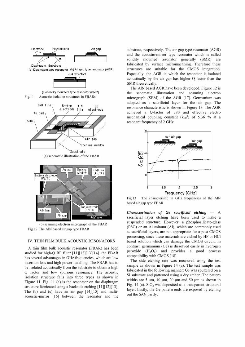
Fig.11 Acoustic isolation structures in FBARs
(a) schematic illustration of the FBAR
(b) scanning electron micrograph of the FBAR Fig.12 The AlN based air gap type FBAR
IV. THIN FILM BULK ACOUSTIC RESONATORS
A thin film bulk acoustic resonator (FBAR) has been studied for high-Q RF filter [11][12][13][14]. the FBAR has several advantages in GHz frequencies, which are low insertion loss and high power handling. The FBAR has to be isolated acoustically from the substrate to obtain a high Q factor and low spurious resonance. The acoustic isolation structure falls into three types as shown in Figure 11. Fig. 11 (a) is the resonator on the diaphragm structure fabricated using a backside etching [11][12][13]. The (b) and (c) have an air gap [14][15] and multi-acoustic-mirror [16] between the resonator and the
substrate, respectively. The air gap type resonator (AGR) and the acoustic-mirror type resonator which is called solidity mounted resonator generally (SMR) are fabricated by surface micromachning. Therefore these structures are suitable for the CMOS integration. Especially, the AGR in which the resonator is isolated acoustically by the air gap has higher Q-factor than the SMR theoretically.
The AlN based AGR have been developed. Figure 12 is the schematic illustration and scanning electron micrograph (SEM) of the AGR [17]. Germanium was adopted as a sacrificial layer for the air gap. The resonance characteristic is shown in Figure 13. The AGR achieved a Q-factor of 780 and effective electro mechanical coupling constant (keff
2) of 5.36 % at a resonant frequency of 2 GHz.
Fig.13 The characteristic in GHz frequencies of the AlN based air gap type FBAR Characterization of Ge sacrificial etching — A sacrificial layer etching have been used to make a suspended structure. However, a phosphosilicate-glass (PSG) or an Aluminum (Al), which are commonly used as sacrificial layers, are not appropriate for a post CMOS processing, since these materials are etched by HF or HCl based solution which can damage the CMOS circuit. In contrast, germanium (Ge) is dissolved easily in hydrogen peroxide (H2O2) and provides a good process compatibility with CMOS [18].
The side etching rate was measured using the test sample as shown in Figure 14 (a). The test sample was fabricated in the following manner: Ge was sputtered on a Si substrate and patterned using a dry etcher. The pattern widths are 5 µm, 10 µm, 20 µm and 50 µm as shown in Fig. 14 (a). SiO2 was deposited as a transparent structural layer. Lastly, the Ge pattern ends are exposed by etching out the SiO2 partly.
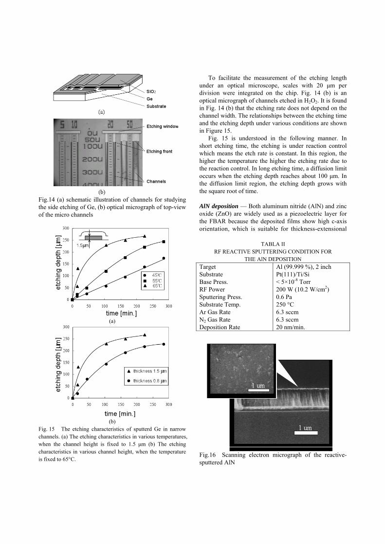
Fig.14 (a) schematic illustration of channels for studying the side etching of Ge, (b) optical micrograph of top-view of the micro channels
(a)
(b) Fig. 15 The etching characteristics of sputterd Ge in narrow channels. (a) The etching characteristics in various temperatures, when the channel height is fixed to 1.5 µm (b) The etching characteristics in various channel height, when the temperature is fixed to 65°C.
To facilitate the measurement of the etching length under an optical microscope, scales with 20 µm per division were integrated on the chip. Fig. 14 (b) is an optical micrograph of channels etched in H2O2. It is found in Fig. 14 (b) that the etching rate does not depend on the channel width. The relationships between the etching time and the etching depth under various conditions are shown in Figure 15.
Fig. 15 is understood in the following manner. In short etching time, the etching is under reaction control which means the etch rate is constant. In this region, the higher the temperature the higher the etching rate due to the reaction control. In long etching time, a diffusion limit occurs when the etching depth reaches about 100 µm. In the diffusion limit region, the etching depth grows with the square root of time.
AlN deposition — Both aluminum nitride (AlN) and zinc oxide (ZnO) are widely used as a piezoelectric layer for the FBAR because the deposited films show high c-axis orientation, which is suitable for thickness-extensional
TABLA II RF REACTIVE SPUTTERING CONDITION FOR
THE AlN DEPOSITION Target Substrate Base Press. RF Power Sputtering Press. Substrate Temp. Ar Gas Rate N2 Gas Rate Deposition Rate
Al (99.999 %), 2 inch Pt(111)/Ti/Si < 5×10⁻⁸ Torr 200 W (10.2 W/cm2) 0.6 Pa 250 °C 6.3 sccm 6.3 sccm 20 nm/min.
Fig.16 Scanning electron micrograph of the reactive-sputtered AlN
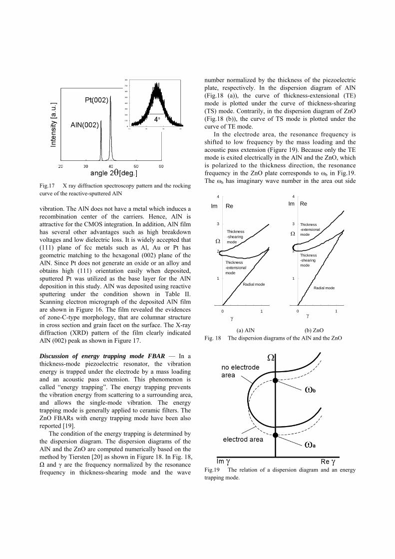
Fig.17 X ray diffraction spectroscopy pattern and the rocking curve of the reactive-sputtered AlN vibration. The AlN does not have a metal which induces a recombination center of the carriers. Hence, AlN is attractive for the CMOS integration. In addition, AlN film has several other advantages such as high breakdown voltages and low dielectric loss. It is widely accepted that (111) plane of fcc metals such as Al, Au or Pt has geometric matching to the hexagonal (002) plane of the AlN. Since Pt does not generate an oxide or an alloy and obtains high (111) orientation easily when deposited, sputtered Pt was utilized as the base layer for the AlN deposition in this study. AlN was deposited using reactive sputtering under the condition shown in Table II. Scanning electron micrograph of the deposited AlN film are shown in Figure 16. The film revealed the evidences of zone-C-type morphology, that are columnar structure in cross section and grain facet on the surface. The X-ray diffraction (XRD) pattern of the film clearly indicated AlN (002) peak as shown in Figure 17. Discussion of energy trapping mode FBAR — In a thickness-mode piezoelectric resonator, the vibration energy is trapped under the electrode by a mass loading and an acoustic pass extension. This phenomenon is called “energy trapping”. The energy trapping prevents the vibration energy from scattering to a surrounding area, and allows the single-mode vibration. The energy trapping mode is generally applied to ceramic filters. The ZnO FBARs with energy trapping mode have been also reported [19].
The condition of the energy trapping is determined by the dispersion diagram. The dispersion diagrams of the AlN and the ZnO are computed numerically based on the method by Tiersten [20] as shown in Figure 18. In Fig. 18, Ω and γ are the frequency normalized by the resonance frequency in thickness-shearing mode and the wave
number normalized by the thickness of the piezoelectric plate, respectively. In the dispersion diagram of AlN (Fig.18 (a)), the curve of thickness-extensional (TE) mode is plotted under the curve of thickness-shearing (TS) mode. Contrarily, in the dispersion diagram of ZnO (Fig.18 (b)), the curve of TS mode is plotted under the curve of TE mode.
In the electrode area, the resonance frequency is shifted to low frequency by the mass loading and the acoustic pass extension (Figure 19). Because only the TE mode is exited electrically in the AlN and the ZnO, which is polarized to the thickness direction, the resonance frequency in the ZnO plate corresponds to ωb in Fig.19. The ωb has imaginary wave number in the area out side
(a) AlN (b) ZnO Fig. 18 The dispersion diagrams of the AlN and the ZnO
Fig.19 The relation of a dispersion diagram and an energy trapping mode.
0
1
2
3
4
-0.2
0 0.2 0.4 0.6 0.8 1 1.2
Re
γ
Im
Ω
Radial mode
Thickness-extensionalmode
Thickness-shearingmode
0
1
2
3
4
-0.2
0 0.2 0.4 0.6 0.8 1 1.2
Im Re
γ
Ω
Radial mode
Thickness-shearingmode
Thickness-extensionalmode
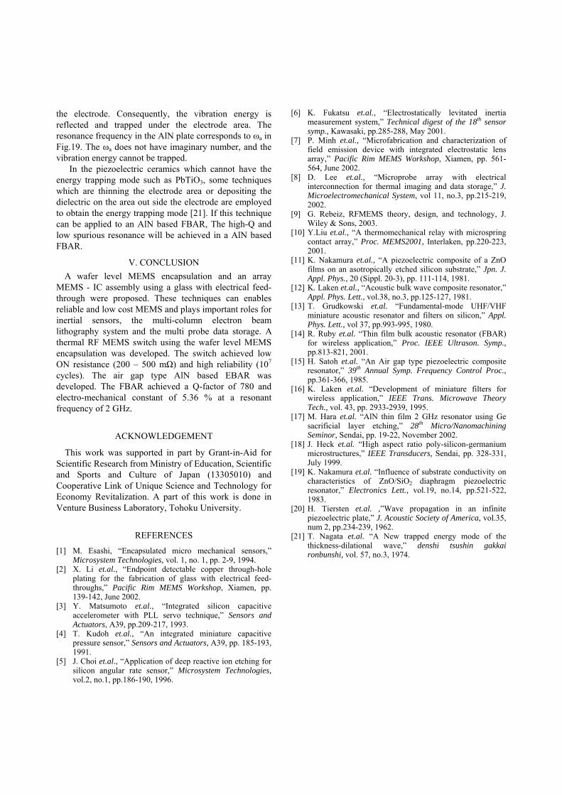
the electrode. Consequently, the vibration energy is reflected and trapped under the electrode area. The resonance frequency in the AlN plate corresponds to ωa in Fig.19. The ωa does not have imaginary number, and the vibration energy cannot be trapped.
In the piezoelectric ceramics which cannot have the energy trapping mode such as PbTiO3, some techniques which are thinning the electrode area or depositing the dielectric on the area out side the electrode are employed to obtain the energy trapping mode [21]. If this technique can be applied to an AlN based FBAR, The high-Q and low spurious resonance will be achieved in a AlN based FBAR.
V. CONCLUSION A wafer level MEMS encapsulation and an array
MEMS - IC assembly using a glass with electrical feed-through were proposed. These techniques can enables reliable and low cost MEMS and plays important roles for inertial sensors, the multi-column electron beam lithography system and the multi probe data storage. A thermal RF MEMS switch using the wafer level MEMS encapsulation was developed. The switch achieved low ON resistance (200 – 500 mΩ) and high reliability (107 cycles). The air gap type AlN based EBAR was developed. The FBAR achieved a Q-factor of 780 and electro-mechanical constant of 5.36 % at a resonant frequency of 2 GHz.
ACKNOWLEDGEMENT
This work was supported in part by Grant-in-Aid for Scientific Research from Ministry of Education, Scientific and Sports and Culture of Japan (13305010) and Cooperative Link of Unique Science and Technology for Economy Revitalization. A part of this work is done in Venture Business Laboratory, Tohoku University.
REFERENCES
[1] M. Esashi, “Encapsulated micro mechanical sensors,” Microsystem Technologies, vol. 1, no. 1, pp. 2-9, 1994.
[2] X. Li et.al., “Endpoint detectable copper through-hole plating for the fabrication of glass with electrical feed-throughs,” Pacific Rim MEMS Workshop, Xiamen, pp. 139-142, June 2002.
[3] Y. Matsumoto et.al., “Integrated silicon capacitive accelerometer with PLL servo technique,” Sensors and Actuators, A39, pp.209-217, 1993.
[4] T. Kudoh et.al., “An integrated miniature capacitive pressure sensor,” Sensors and Actuators, A39, pp. 185-193, 1991.
[5] J. Choi et.al., “Application of deep reactive ion etching for silicon angular rate sensor,” Microsystem Technologies, vol.2, no.1, pp.186-190, 1996.
[6] K. Fukatsu et.al., “Electrostatically levitated inertia measurement system,” Technical digest of the 18th sensor symp., Kawasaki, pp.285-288, May 2001.
[7] P. Minh et.al., “Microfabrication and characterization of field emission device with integrated electrostatic lens array,” Pacific Rim MEMS Workshop, Xiamen, pp. 561-564, June 2002.
[8] D. Lee et.al., “Microprobe array with electrical interconnection for thermal imaging and data storage,” J. Microelectromechanical System, vol 11, no.3, pp.215-219, 2002.
[9] G. Rebeiz, RFMEMS theory, design, and technology, J. Wiley & Sons, 2003.
[10] Y.Liu et.al., “A thermomechanical relay with microspring contact array,” Proc. MEMS2001, Interlaken, pp.220-223, 2001.
[11] K. Nakamura et.al., “A piezoelectric composite of a ZnO films on an asotropically etched silicon substrate,” Jpn. J. Appl. Phys., 20 (Sippl. 20-3), pp. 111-114, 1981.
[12] K. Laken et.al., “Acoustic bulk wave composite resonator,” Appl. Phys. Lett., vol.38, no.3, pp.125-127, 1981.
[13] T. Grudkowski et.al. “Fundamental-mode UHF/VHF miniature acoustic resonator and filters on silicon,” Appl. Phys. Lett., vol 37, pp.993-995, 1980.
[14] R. Ruby et.al. “Thin film bulk acoustic resonator (FBAR) for wireless application,” Proc. IEEE Ultrason. Symp., pp.813-821, 2001.
[15] H. Satoh et.al. “An Air gap type piezoelectric composite resonator,” 39th Annual Symp. Frequency Control Proc., pp.361-366, 1985.
[16] K. Laken et.al. “Development of miniature filters for wireless application,” IEEE Trans. Microwave Theory Tech., vol. 43, pp. 2933-2939, 1995.
[17] M. Hara et.al. “AlN thin film 2 GHz resonator using Ge sacrificial layer etching,” 28th Micro/Nanomachining Seminor, Sendai, pp. 19-22, November 2002.
[18] J. Heck et.al. “High aspect ratio poly-silicon-germanium microstructures,” IEEE Transducers, Sendai, pp. 328-331, July 1999.
[19] K. Nakamura et.al. “Influence of substrate conductivity on characteristics of ZnO/SiO2 diaphragm piezoelectric resonator,” Electronics Lett., vol.19, no.14, pp.521-522, 1983.
[20] H. Tiersten et.al. ,”Wave propagation in an infinite piezoelectric plate,” J. Acoustic Society of America, vol.35, num 2, pp.234-239, 1962.
[21] T. Nagata et.al. “A New trapped energy mode of the thickness-dilational wave,” denshi tsushin gakkai ronbunshi, vol. 57, no.3, 1974.


