Embed Size (px)
Citation preview
August, 2016 Microwave Review
17
Full-wave Analysis and Characterization of RF Package for MEMS Applications
Ayan Karmakar, Kamaljeet Singh
Abstract - This article details about package analysis of RF-MEMS based devices for Ka-band applications. Standard cavity package has been taken into consideration. FEM based electromagnetic solver Ansys HFSS suite is utilized for this purpose. Constraints related to Ka-band and its possible remedies are discussed. Eigen-mode analysis and loss characterization have been done using HFSS. Possible causes of RF losses at 30 ± 1 GHz have been investigated. Further, new package configuration with recommended features, yielding better simulated RF performances is presented in this work. Practically, the package has been characterized.
Keywords - Cavity package, Bond wire, Eigen mode and
transition.
I. INTRODUCTION
A significant progress in design and fabrication process for MEMS (Micro Electro Mechanical System) technology has been observed in the last few decades. But, the only bottleneck of this new technology is its packaging topology directing towards reliability constraints. Unlike the other microelectronics (VLSI/ULSI) devices, the specialty for MEMS packages is to support free-hanging mechanical tiny structures. Usually, the main functions of packages are: providing mechanical support, protection from surrounding environment and building electrical interconnection to other system components [1-3]. Traditionally for many years, RF devices have been packaged in metal-can, ceramic and cerdip cavity packages. Among these, cavity packaging for the RF is most proffered in the consideration of providing headspace for raised surface features, such as air-bridges and protects elements such as RF MEMS switch, Phase Shifter, filter, resonators or any reconfigurable devices, etc [4-8]. The present work primarily demonstrates a standard cavity package modified for RF MEMS application. This article also highlights various approaches adopted to mitigate losses introduced in its assembly working at Ka-band.
Along with the insertion and dielectric losses associated with the circuit, radiation losses also come into picture predominantly at this higher side of microwave band.
An FEM based simulation study is carried out for this whole research work. Contribution of each building block has been investigated in detail and further complete loss analysis is accomplished.
Ayan Karmakar and Kamaljeet Singh are working in Semi-Conductor Laboratory (SCL), Punjab, India. E-mail: [email protected]
II. PACKAGE CONFIGURATION
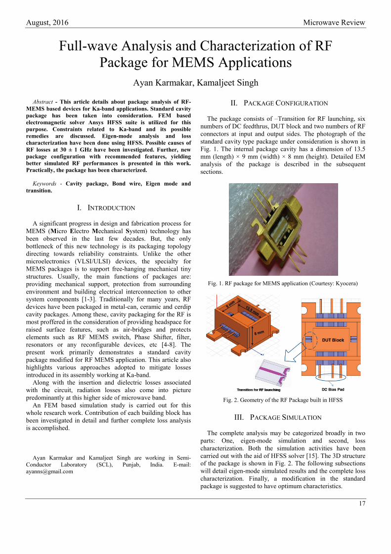
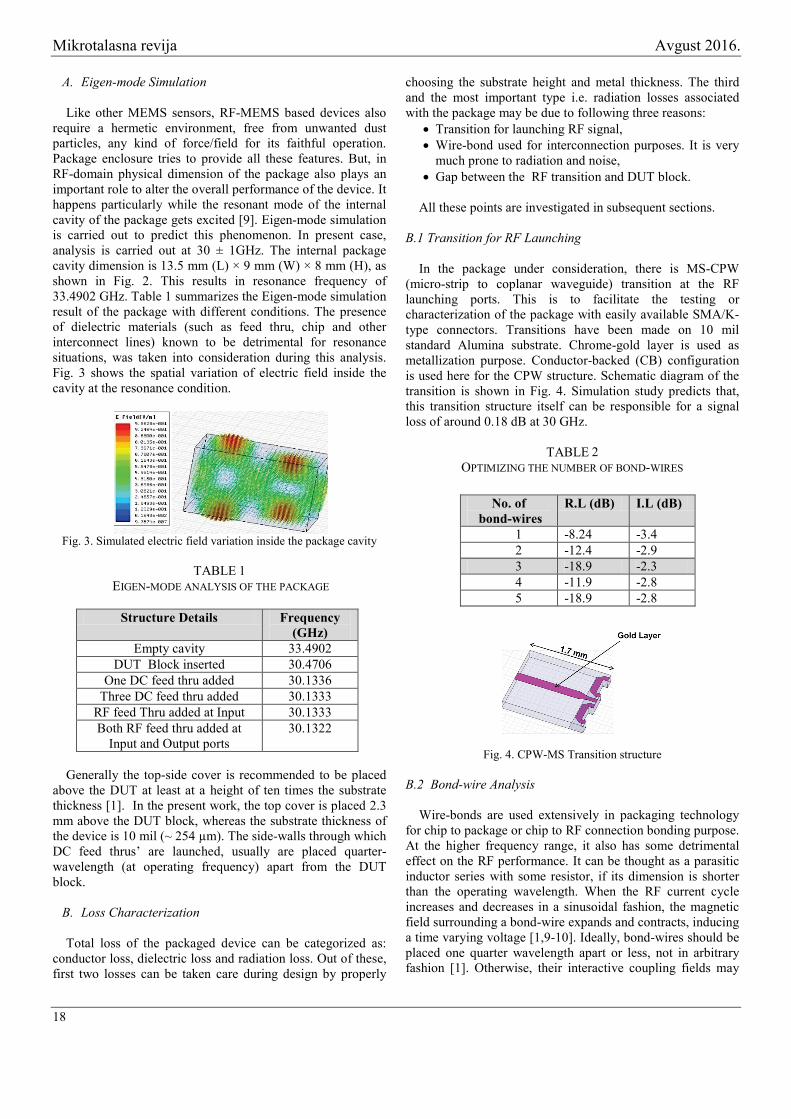
The package consists of –Transition for RF launching, six numbers of DC feedthrus, DUT block and two numbers of RF connectors at input and output sides. The photograph of the standard cavity type package under consideration is shown in Fig. 1. The internal package cavity has a dimension of 13.5 mm (length) × 9 mm (width) × 8 mm (height). Detailed EM analysis of the package is described in the subsequent sections.
Fig. 1. RF package for MEMS application (Courtesy: Kyocera)
Fig. 2. Geometry of the RF Package built in HFSS
III. PACKAGE SIMULATION
The complete analysis may be categorized broadly in two parts: One, eigen-mode simulation and second, loss characterization. Both the simulation activities have been carried out with the aid of HFSS solver [15]. The 3D structure of the package is shown in Fig. 2. The following subsections will detail eigen-mode simulated results and the complete loss characterization. Finally, a modification in the standard package is suggested to have optimum characteristics.
Mikrotalasna revija Avgust 2016.
18
A. Eigen-mode Simulation
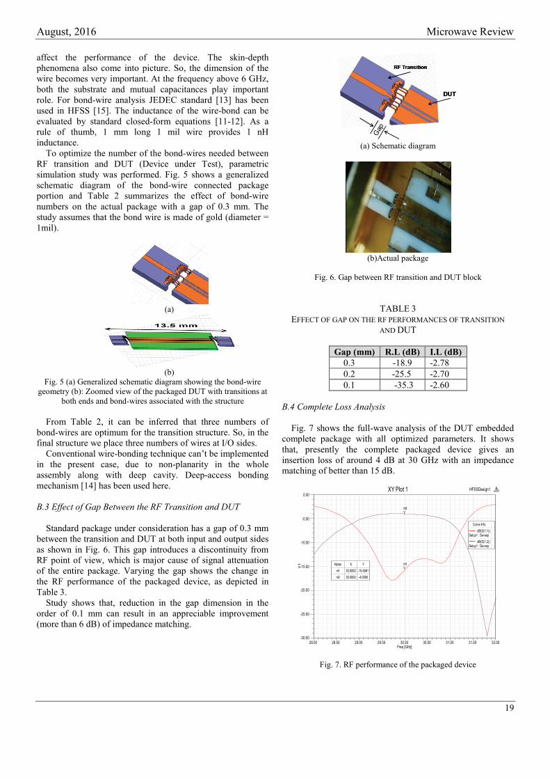
Like other MEMS sensors, RF-MEMS based devices also require a hermetic environment, free from unwanted dust particles, any kind of force/field for its faithful operation. Package enclosure tries to provide all these features. But, in RF-domain physical dimension of the package also plays an important role to alter the overall performance of the device. It happens particularly while the resonant mode of the internal cavity of the package gets excited [9]. Eigen-mode simulation is carried out to predict this phenomenon. In present case, analysis is carried out at 30 ± 1GHz. The internal package cavity dimension is 13.5 mm (L) × 9 mm (W) × 8 mm (H), as shown in Fig. 2. This results in resonance frequency of 33.4902 GHz. Table 1 summarizes the Eigen-mode simulation result of the package with different conditions. The presence of dielectric materials (such as feed thru, chip and other interconnect lines) known to be detrimental for resonance situations, was taken into consideration during this analysis. Fig. 3 shows the spatial variation of electric field inside the cavity at the resonance condition.
Fig. 3. Simulated electric field variation inside the package cavity
TABLE 1
EIGEN-MODE ANALYSIS OF THE PACKAGE
Structure Details Frequency (GHz)
Empty cavity 33.4902 DUT Block inserted 30.4706
One DC feed thru added 30.1336 Three DC feed thru added 30.1333
RF feed Thru added at Input 30.1333 Both RF feed thru added at
Input and Output ports 30.1322
Generally the top-side cover is recommended to be placed
above the DUT at least at a height of ten times the substrate thickness [1]. In the present work, the top cover is placed 2.3 mm above the DUT block, whereas the substrate thickness of the device is 10 mil (~ 254 µm). The side-walls through which DC feed thrus’ are launched, usually are placed quarter-wavelength (at operating frequency) apart from the DUT block.
B. Loss Characterization
Total loss of the packaged device can be categorized as: conductor loss, dielectric loss and radiation loss. Out of these, first two losses can be taken care during design by properly
choosing the substrate height and metal thickness. The third and the most important type i.e. radiation losses associated with the package may be due to following three reasons:
• Transition for launching RF signal, • Wire-bond used for interconnection purposes. It is very
much prone to radiation and noise, • Gap between the RF transition and DUT block.
All these points are investigated in subsequent sections.
B.1 Transition for RF Launching
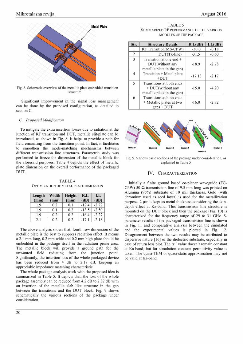
In the package under consideration, there is MS-CPW (micro-strip to coplanar waveguide) transition at the RF launching ports. This is to facilitate the testing or characterization of the package with easily available SMA/K-type connectors. Transitions have been made on 10 mil standard Alumina substrate. Chrome-gold layer is used as metallization purpose. Conductor-backed (CB) configuration is used here for the CPW structure. Schematic diagram of the transition is shown in Fig. 4. Simulation study predicts that, this transition structure itself can be responsible for a signal loss of around 0.18 dB at 30 GHz.
TABLE 2
OPTIMIZING THE NUMBER OF BOND-WIRES
Fig. 4. CPW-MS Transition structure
B.2 Bond-wire Analysis
Wire-bonds are used extensively in packaging technology for chip to package or chip to RF connection bonding purpose. At the higher frequency range, it also has some detrimental effect on the RF performance. It can be thought as a parasitic inductor series with some resistor, if its dimension is shorter than the operating wavelength. When the RF current cycle increases and decreases in a sinusoidal fashion, the magnetic field surrounding a bond-wire expands and contracts, inducing a time varying voltage [1,9-10]. Ideally, bond-wires should be placed one quarter wavelength apart or less, not in arbitrary fashion [1]. Otherwise, their interactive coupling fields may
No. of bond-wires
R.L (dB) I.L (dB)
1 -8.24 -3.4 2 -12.4 -2.9 3 -18.9 -2.3 4 -11.9 -2.8 5 -18.9 -2.8
August, 2016 Microwave Review
19
affect the performance of the device. The skin-depth phenomena also come into picture. So, the dimension of the wire becomes very important. At the frequency above 6 GHz, both the substrate and mutual capacitances play important role. For bond-wire analysis JEDEC standard [13] has been used in HFSS [15]. The inductance of the wire-bond can be evaluated by standard closed-form equations [11-12]. As a rule of thumb, 1 mm long 1 mil wire provides 1 nH inductance.
To optimize the number of the bond-wires needed between RF transition and DUT (Device under Test), parametric simulation study was performed. Fig. 5 shows a generalized schematic diagram of the bond-wire connected package portion and Table 2 summarizes the effect of bond-wire numbers on the actual package with a gap of 0.3 mm. The study assumes that the bond wire is made of gold (diameter = 1mil).
(a)
(b)
Fig. 5 (a) Generalized schematic diagram showing the bond-wire geometry (b): Zoomed view of the packaged DUT with transitions at
both ends and bond-wires associated with the structure
From Table 2, it can be inferred that three numbers of bond-wires are optimum for the transition structure. So, in the final structure we place three numbers of wires at I/O sides.
Conventional wire-bonding technique can’t be implemented in the present case, due to non-planarity in the whole assembly along with deep cavity. Deep-access bonding mechanism [14] has been used here. B.3 Effect of Gap Between the RF Transition and DUT
Standard package under consideration has a gap of 0.3 mm
between the transition and DUT at both input and output sides as shown in Fig. 6. This gap introduces a discontinuity from RF point of view, which is major cause of signal attenuation of the entire package. Varying the gap shows the change in the RF performance of the packaged device, as depicted in Table 3.
Study shows that, reduction in the gap dimension in the order of 0.1 mm can result in an appreciable improvement (more than 6 dB) of impedance matching.
(a) Schematic diagram
(b)Actual package
Fig. 6. Gap between RF transition and DUT block
TABLE 3 EFFECT OF GAP ON THE RF PERFORMANCES OF TRANSITION
AND DUT
Gap (mm) R.L (dB) I.L (dB) 0.3 -18.9 -2.78 0.2 -25.5 -2.70 0.1 -35.3 -2.60
B.4 Complete Loss Analysis
Fig. 7 shows the full-wave analysis of the DUT embedded complete package with all optimized parameters. It shows that, presently the complete packaged device gives an insertion loss of around 4 dB at 30 GHz with an impedance matching of better than 15 dB.
Fig. 7. RF performance of the packaged device
28.00 28.50 29.00 29.50 30.00 30.50 31.00 31.50 32.00Freq [GHz]
-30.00
-25.00
-20.00
-15.00
-10.00
-5.00
0.00
Y1
HFSSDesign1XY Plot 1 ANSOFT
m1
m2
Curve InfodB(S(1,1))
Setup1 : Sw eepdB(S(1,2))
Setup1 : Sw eep
Name X Ym1 30.0000 -15.6981m2 30.0000 -4.0000
Mikrotalasna revija Avgust 2016.
20
Fig. 8. Schematic overview of the metallic plate embedded transition structure
Significant improvement in the signal loss management
can be done by the proposed configuration, as detailed in section C.
C. Proposed Modification
To mitigate the extra insertion losses due to radiation at the
junction of RF transition and DUT, metallic slit/plate can be introduced, as shown in Fig. 8. It helps to provide a path for field emanating from the transition point. In fact, it facilitates to smoothen the mode-matching mechanisms between different transmission line structures. Parametric study was performed to freeze the dimension of the metallic block for the aforesaid purposes. Table 4 depicts the effect of metallic plate dimension on the overall performance of the packaged DUT.
TABLE 4
OPTIMIZATION OF METAL PLATE DIMENSION
Length (mm)
Width (mm)
Height (mm)
R.L (dB)
I.L (dB)
1.9 0.2 0.1 -12.4 -2.72 1.9 0.1 0.2 -13.5 -2.50 1.9 0.2 0.2 -16.4 -2.27 2.1 0.2 0.2 -17.1 -2.18
The above analysis shows that, fourth row dimension of the
metallic plate is the best to suppress radiation effect. It means a 2.1 mm long, 0.2 mm wide and 0.2 mm high plate should be embedded in the package itself in the radiation prone area. The metallic block will provide a ground path for the unwanted field radiating from the junction point. Significantly, the insertion loss of the whole packaged device has been reduced from 4 dB to 2.18 dB, keeping an appreciable impedance matching characteristic.
The whole package analysis work with the proposed idea is summarized in Table 5. It depicts that, the loss of the whole package assembly can be reduced from 4.2 dB to 2.82 dB with an insertion of the metallic slab like structure in the gap between the transitions and the DUT block. Fig. 9 shows schematically the various sections of the package under consideration.
TABLE 5 SUMMARIZED RF PERFORMANCE OF THE VARIOUS
MODULES OF THE PACKAGE
Str. Structure Details R.L(dB) I.L(dB) 1 RF Transition(MS-CPW) -30.0 -0.18 2 DUT(Tx-line) -31.5 -0.60 3 Transition at one end +
DUT(without any metallic plate in the gap)
-18.9 -2.78
4 Transition + Metal plate +DUT -17.13 -2.17
5 Transitions at both ends + DUT(without any
metallic plate in the gap) -15.0 -4.20
6 Transitions at both ends + Metallic plates at two
gaps + DUT -16.0 -2.82
Fig. 9. Various basic sections of the package under consideration, as
explained in Table 5
IV. CHARACTERIZATION
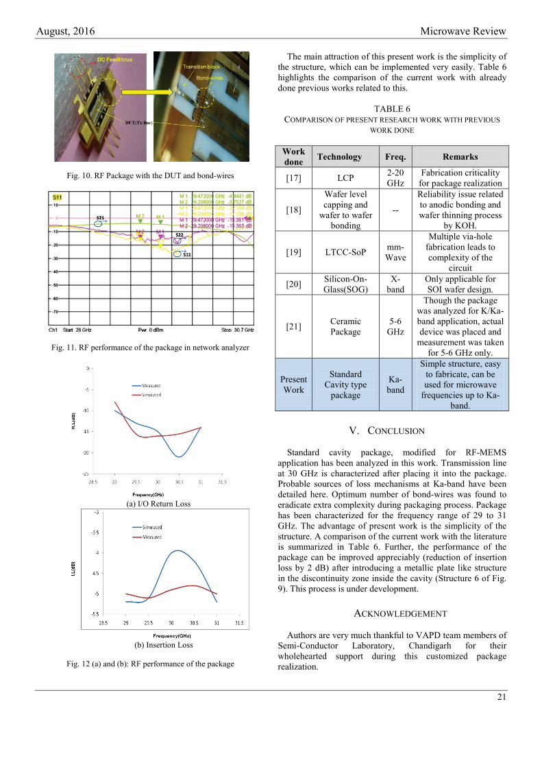
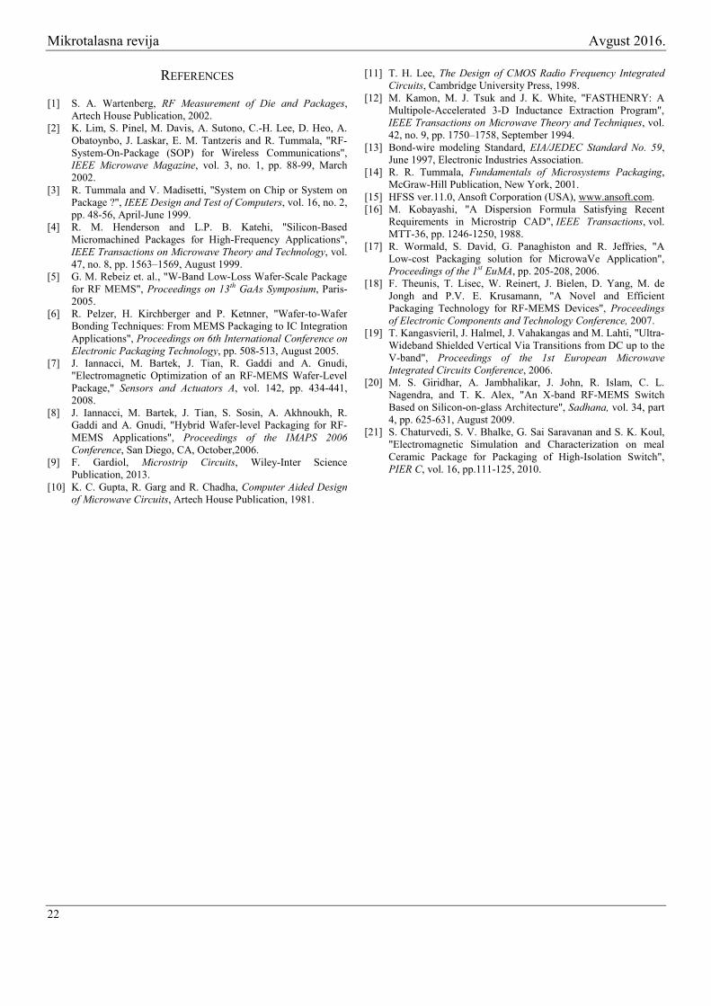
Initially a finite ground based co-planar waveguide (FG-CPW) 50 Ω transmission line of 9.5 mm long was printed on Alumina (96%) substrate of 10 mil thickness. Gold (with chromium used as seed layer) is used for the metallization purpose. 2 µm is kept as metal thickness considering the skin-depth effect at Ka-band. This transmission line structure is mounted on the DUT block and then the package (Fig. 10) is characterized for the frequency range of 29 to 31 GHz. S-parameter results of the packaged transmission line is shown in Fig. 11 and comparative analysis between the simulated and the experimental values is plotted in Fig. 12. Disagreement between the two results may be attributed to dispersive nature [16] of the dielectric substrate, especially in case of return loss plot. The ‘εr’ value doesn’t remain constant at Ka-band, but for simulation constant permittivity value is taken. The quasi-TEM or quasi-static approximation may not be valid at Ka-band.
August, 2016 Microwave Review
21
Fig. 10. RF Package with the DUT and bond-wires
Fig. 11. RF performance of the package in network analyzer
(a) I/O Return Loss
(b) Insertion Loss
Fig. 12 (a) and (b): RF performance of the package
Тhe main attraction of this present work is the simplicity of the structure, which can be implemented very easily. Table 6 highlights the comparison of the current work with already done previous works related to this.
TABLE 6
COMPARISON OF PRESENT RESEARCH WORK WITH PREVIOUS WORK DONE
Work done Technology Freq. Remarks
[17] LCP 2-20 GHz
Fabrication criticality for package realization
[18]
Wafer level capping and
wafer to wafer bonding
--
Reliability issue related to anodic bonding and wafer thinning process
by KOH.
[19] LTCC-SoP mm-Wave
Multiple via-hole fabrication leads to complexity of the
circuit
[20] Silicon-On-Glass(SOG)
X-band
Only applicable for SOI wafer design.
[21] Ceramic Package
5-6 GHz
Though the package was analyzed for K/Ka-band application, actual device was placed and
measurement was taken for 5-6 GHz only.
Present Work
Standard Cavity type
package
Ka-band
Simple structure, easy to fabricate, can be used for microwave
frequencies up to Ka-band.
V. CONCLUSION
Standard cavity package, modified for RF-MEMS application has been analyzed in this work. Transmission line at 30 GHz is characterized after placing it into the package. Probable sources of loss mechanisms at Ka-band have been detailed here. Optimum number of bond-wires was found to eradicate extra complexity during packaging process. Package has been characterized for the frequency range of 29 to 31 GHz. The advantage of present work is the simplicity of the structure. A comparison of the current work with the literature is summarized in Table 6. Further, the performance of the package can be improved appreciably (reduction of insertion loss by 2 dB) after introducing a metallic plate like structure in the discontinuity zone inside the cavity (Structure 6 of Fig. 9). This process is under development.
ACKNOWLEDGEMENT
Authors are very much thankful to VAPD team members of Semi-Conductor Laboratory, Chandigarh for their wholehearted support during this customized package realization.
Mikrotalasna revija Avgust 2016.
22
REFERENCES
[1] S. A. Wartenberg, RF Measurement of Die and Packages, Artech House Publication, 2002.
[2] K. Lim, S. Pinel, M. Davis, A. Sutono, C.-H. Lee, D. Heo, A. Obatoynbo, J. Laskar, E. M. Tantzeris and R. Tummala, "RF-System-On-Package (SOP) for Wireless Communications", IEEE Microwave Magazine, vol. 3, no. 1, pp. 88-99, March 2002.
[3] R. Tummala and V. Madisetti, "System on Chip or System on Package ?", IEEE Design and Test of Computers, vol. 16, no. 2, pp. 48-56, April-June 1999.
[4] R. M. Henderson and L.P. B. Katehi, "Silicon-Based Micromachined Packages for High-Frequency Applications", IEEE Transactions on Microwave Theory and Technology, vol. 47, no. 8, pp. 1563–1569, August 1999.
[5] G. M. Rebeiz et. al., "W-Band Low-Loss Wafer-Scale Package for RF MEMS", Proceedings on 13th GaAs Symposium, Paris-2005.
[6] R. Pelzer, H. Kirchberger and P. Ketnner, "Wafer-to-Wafer Bonding Techniques: From MEMS Packaging to IC Integration Applications", Proceedings on 6th International Conference on Electronic Packaging Technology, pp. 508-513, August 2005.
[7] J. Iannacci, M. Bartek, J. Tian, R. Gaddi and A. Gnudi, "Electromagnetic Optimization of an RF-MEMS Wafer-Level Package," Sensors and Actuators A, vol. 142, pp. 434-441, 2008.
[8] J. Iannacci, M. Bartek, J. Tian, S. Sosin, A. Akhnoukh, R. Gaddi and A. Gnudi, "Hybrid Wafer-level Packaging for RF-MEMS Applications", Proceedings of the IMAPS 2006 Conference, San Diego, CA, October,2006.
[9] F. Gardiol, Microstrip Circuits, Wiley-Inter Science Publication, 2013.
[10] K. C. Gupta, R. Garg and R. Chadha, Computer Aided Design of Microwave Circuits, Artech House Publication, 1981.
[11] T. H. Lee, The Design of CMOS Radio Frequency Integrated Circuits, Cambridge University Press, 1998.
[12] M. Kamon, M. J. Tsuk and J. K. White, "FASTHENRY: A Multipole-Accelerated 3-D Inductance Extraction Program", IEEE Transactions on Microwave Theory and Techniques, vol. 42, no. 9, pp. 1750–1758, September 1994.
[13] Bond-wire modeling Standard, EIA/JEDEC Standard No. 59, June 1997, Electronic Industries Association.
[14] R. R. Tummala, Fundamentals of Microsystems Packaging, McGraw-Hill Publication, New York, 2001.
[15] HFSS ver.11.0, Ansoft Corporation (USA), www.ansoft.com. [16] M. Kobayashi, "A Dispersion Formula Satisfying Recent
Requirements in Microstrip CAD", IEEE Transactions, vol. MTT-36, pp. 1246-1250, 1988.
[17] R. Wormald, S. David, G. Panaghiston and R. Jeffries, "A Low-cost Packaging solution for MicrowaVe Application", Proceedings of the 1st EuMA, pp. 205-208, 2006.
[18] F. Theunis, T. Lisec, W. Reinert, J. Bielen, D. Yang, M. de Jongh and P.V. E. Krusamann, "A Novel and Efficient Packaging Technology for RF-MEMS Devices", Proceedings of Electronic Components and Technology Conference, 2007.
[19] T. Kangasvieril, J. Halmel, J. Vahakangas and M. Lahti, "Ultra-Wideband Shielded Vertical Via Transitions from DC up to the V-band", Proceedings of the 1st European Microwave Integrated Circuits Conference, 2006.
[20] M. S. Giridhar, A. Jambhalikar, J. John, R. Islam, C. L. Nagendra, and T. K. Alex, "An X-band RF-MEMS Switch Based on Silicon-on-glass Architecture", Sadhana, vol. 34, part 4, pp. 625-631, August 2009.
[21] S. Chaturvedi, S. V. Bhalke, G. Sai Saravanan and S. K. Koul, "Electromagnetic Simulation and Characterization on meal Ceramic Package for Packaging of High-Isolation Switch", PIER C, vol. 16, pp.111-125, 2010.