Embed Size (px)
Citation preview
E D U L A N : A L O C A L A R E A N E T W O R K F O R
A N
E D U C A T I O N A L E N V I R O N M E N T
Eduardo Albino De Souza
A dissertation submitted to the Faculty of Engineering, University of the
Witwatersrand, Johannesburg, in fulfilment of the requirements for the
degree of Master of Science in Engineering.
D E C L A R A T IO N
I declare that this disscrta. ion is my own, unaided work. It is being
submitted for the Degree of Master of Science in the University of the
Witwatersrand, Johannesburg. It has not been submitted before for any
degree or examinat ion in any other University.
g <>■ t''
E. A. DE SOUZA
On this the 16'th day of Mai c
Declaration ii

A B S T R A C T
Thv needs and requirements of a typical Personal Computer (P.C.) network
in an iduc.ttional envt ronment are discussed A proposed system with a
- t ir-bus topology with a f ile-server at the hub is described. Each ray
of the star lr- a 422 twisted pair us onto which a number of personal
iters ilti attached. Access to the bus is by means of the CSMA CA
(Carrier Sense Multiple Ao ess with Collision Avoidance)access method.
The bt.sses operate at bit rates of between 1 and 1.5 Mbits per second.
The interfile t the Personal Computer is by means of a floppy disk drive
• ;l:»tut The principles of ope r it ion of the floppy disk drive system in
a Personal Computer are described <is well as the design and implementation
i i test inn if the disk drive emulator. Development of a device driver
to :e»t»* i : nber of logical drives on each Personal Computer with as
sociate] drives on the f i le-server is described.
Abstract iii

ACKNOWLEDGEMENTS
I wish to express my thanks to:
o Mr. G. T. Gray who supervised my project, for his suppor' tn-i V<-lp,
for the discussions we have had, and tor the eat av .onomy I have
had in my work.
o Professor H. E. H.mrahun for hi - ss: stun e n > ttie d'scuasions we
had.
o
cial assistance by way of a bursary durinjt my period of resear
o Mr. S. Marantos whose assistance in a numiier of aspects is greatly
appreciated.
• Mr. R . A . Schut■ f01for novice Pascal programmers which is to be implemented on the
f i le-server.
o Mr. M. W. Hildyard For his res* irch into the high level software for
the f i lo-server.
o I am also grateful to those labo.ntory te hni ians, who by their
valuable advice, have helped me in th.s project
Acknow1edguments iv

TA B L E OF C O N T E N T S
1 .0 IN T R O D U C T IO N .................................................................................................. 1
2 . 0 NETWORKS IN AN E D U C A T IO N A L E N V IR O N M E N T : ARE T H E Y
NECESSARY? ..................................................................................................................... 2
3 . 0 NETWORKS FOR E D U C A T IO N A L E N V IR O N M E N T S : WHY ARE T H E Y
D IFFE R E N T? ..................................................................................................................... 4
4 . 0 NETWORK REQUIREM ENTS .......................................................................... 6
5 . 0 SYSTEM O VERVIEW ............................................................................................. 7
5 .1 Use of one P . C . with the f loppy disk d r iv e emulator connected
to the f i l e - s e r v e r . Only one f loppy disk is emula ted . 10
5 .2 Emulation of 25 f loppy disk dr ives using the hardware c o n f ig
urat ion in ( 5 . 1 ) ............................................................................................................................12
5 .3 The operation of the menu program and software protection on
the system described in ( 5 . 2 ) a b o ve ........................................................................... 13
5 .4 A number of P . C . ’s operat ing as in ( 5 . 3 ) a bove ...................................... 15
6 . 0 THE FLOPPY DISK D R IV E EMULATOR ........................................................ 16
6.1 The Floppy Disk D r ive Emulator (H a r d w a r e ) ......................................19
6 . 2 The Floppy Disk D r ive Emulator ( Software) ..........................................23
7 .0 REQUIREMENTS OF THE F IL E -S ER VE R ................................................... 28
8 . 0 C O NCLU SIO N ............................................................................................................... 30
A P P E N D IX A THE S T R U C T U R E OF FLOPPY DISKS .......................................... 33
Table of Contents v
A P P EN D IX B THE FLOPPY DISK D R IV E INTER FA C E . . .
A P P EN D IX C THE FLOPPY DISK C O N T R O L L E R .......................
A P P EN D IX D DA TA RECORDING T E C H N IO U E S .......................
A P P E N D IX E THE DECODER C I R C U I T R Y .....................................
A P P E N D IX F THE ENCODER C I R C U I T R Y .....................................
A P P EN D IX G THE IN TE R FA C E BOARD ..........................................
A PPEN D IX H THE MICROPROCESSOR C O N T R O L L E R U N I T
A P P EN D IX I THE T R A C K CACHE ...................................................
A P P EN D IX J WHY STAR-BUS" N O T E T H E R N E T ...................
A PFEN D IX K THE CSMA CA ACCESS PROTOCOL ...................
A P P EN D IX L MESSAGE PASSING ON T R A C K 40 ...................
AP P E N D IX M THE MS-DOS DEVIC E D R IV E R ............................
A PPEN D IX N THE ENVIS AGED FILE SERVER HARDWARE
A P P EN D IX O EM ULATION SOFTWARE ..........................................
A P P EN D IX P THE TR A C K E M ULAT IO N SOFTWARE . . . .
A P P EN D IX 0 T E S T IN G THE FLOPPY D ISK D R IVE EMULATOR
Tdbli- of Contents
L IS T OF REFERENCES
B IB L IO G R A P H Y
Table of Contents
L IS T OF FIGURES
Figure
5.1 Schematic Diagram Of The 1Star-bus1 Network
Topology .......................................
5.2 Schematic Diagram Of The Configuration For The
Emulation Of a Single Floppy Disk .............
5.3 Schematic Diagram Of The Configuration For The
Emulation Of 25 Floppy Disks ....... ..........
5.4 Logical Association And Physical Mapping Of The
Disk Drives On The P.C. And The File-server ...
6.1 Components Comprising The Floppy Disk System In
The P.C............................................
6.2 Flow Of Data In And Out Of The Emulator .........
6.3 Schematic Diagram Of The Emulator Track Counter
6.4 Flow-chart Of The Emulator Software.............
A . 1 Subdivision Of The Disk Surface Into A Number Of
Tracks .............................................
A.2 Diagram Of The IBM SysV 34 Double Density Track
Format ...........................................
A.3 Composition Of A Sector ..........................
D.l Diagram Illustrating FM And MFM Encoding ........
D.2 Encoding Of The Address And 1 I) Address Markers .
F..1 The Decoder Circuit Diagram ......................
E.2 Timing Diagram Of The Counter Reset Circuit ...
E.3 Timing Diagram Of Write Data At The Start Of A
Write Operation ...................................
List Of Figures
.— /i
E .4 Timing Diagram Of Clock Pulies Showing Expanded
Pulses And Added Clock Pulses ....................
F.l Bit Cell Structure - Pulses May Occur During The
First And Third Microsecond ......................
F.2 Encoding Of The Address And I.D. Address Markers .
F.3 Counter Output Waveforms .........................
F.4 The Encoder Circuit Diagram ......................
G.l The Interface Circuit Diagram ....................
H.l Block Diagram Of The Floppy Di*k Drive Emulator
H .2 The 80188 CPU Circuit Diagram ....................
H.3 The Memory Circuit Diagram .......................
H.A The Memory Map Of The 80188 ......................H.5 Timing Diagram Of The RAS, CAS And WE signals ....
M.6 The I/O Circuit Diagram ..........................
H .7 The I/O Map .......................................
I.1 Cache Implementation With Each Data Segment
Preceded By A Header ............................
1.2 Separate Index Ani Data Areas For The Cache .....
1.3 Diagrammatic Represent ion Of The Track Cache Data
Structure .... ............ .......... .............
K.l Timing Of A CSMA CA Network Dialogue .............
K.2 CSMA CA Frame Format .............................
P.l Diagram Of The IBM System 34 Double Density Track
Format ............................................
P.2 Bit Functions Of Write Register i 01 The CM530 ...
List Of Figures
1.0 i n t r o d u c t i o n
l.B.M.'s launch of its Personal Computer (P.C.) in 1981 and the subse
quent flood of P.C. clones on the market has accelerated the use of com
puters in a number of fields and education is no exception. A number of
networks have been designed for these P.C. s for commercial use but the
design of networks for use in educational environments presents certain
design challenges that are rarely encountered n other environments.
In this dissertation the necessity of a network system in an educational
environment is discussed as well a^ the aspects that make these networks
different to others. A 'star-bus' topology is proposed with a file-server
at the hub. Access to each of the rays of the star which consist of an
RS422 twisted pair operating at speeds between 1 and 1.5 Mbits per second
is by means of the CilMA CA access method. A novel approach has been
adopted whereby the interface between the P.C. and the network is by means
of the floppy disk drive system of the machine. This hardware approach
along with a small amount of software makes the network appear to the P.C.
as a number of disk drives. A degree of software protection is included
to reduce the possibility of software on the file-server being copied.
The design, implementation and testing of the P.C. interface comprised
the major portion of the research and hence forms the major part of the
dissertation. Aspects such as network media access, requirements of the
file-server and software protection are also discussed.
Due to the extremely technical naturt of most of the descriptions, a large
number of there descriptions have been placed in the appendices to make
the main body of the report easier to read. The P.C.'s referred to in a
number of places in the report refer to the I.H.M. and compatible Personal
Computers. These machines operate primarily on the PC-DOS and MS-DOS op
erating systems.
Introduction 1

2 . 0 NETWORKS IN AN E D U C A T IO N A L E N V IR O N M E N T : ARE T H E Y NECESSARY?
To answor the question 'Arp notwotks necessary in an educational envi
ronment ' consider a set of comp ter* used in an educAtional laboratory,
and the advantages which will be provided by adding a network.
A Personal Computer (P.C.) laboratory is equipped with between 25 and 40
computers. Each of these computers has two floppy-disks and no hard-disk.
This laboratory may be require i to serve more than 100 students in total.
During this computer course the students ire required to do certain lab
oratory exercises, prepare assignments and write tests. One may initially
think that it is a s-'triple task to provide each of the computers with a
'Master Disk' which has the required Disk Operating System (DOS) along
with the necessary laboratory exercises or assignment. If we stop to
consider the lire required to prepare these master disks we soon realise
that the preparation of 40 such disks is a tedious task. We must be re
alistic since as experience has shown, it is rare that these exercises
are fault free. As the exercis** is carried out, invariably errors are
found that have to be corrected. We are now confronted again with the
master disk preparation ta'ik.
It would be far more efficient for one master disk to be corrected and
be available immediately to the students. This would certainly be possible
if these masters were kept on a central lile server to which all the
students had ai.ciss via each P.C. The network would thus bi» required to
provide the interconnection between the file server and each individual
P.C..
Another aspect mentioned above viz. the writing of tests would benefit
by the use of a network. Considering the number of students mentioned
above wi- must examine tin* effort required by the examiners in such an
Networks In An Educational Environment: Are They Necessary? 2
n. _ _ _ > •/">

exercise. In -nost cases each student requires two floppy disks for the
test in addition to the disk which contains the test itself. If a network
was available there would only have to he one test master disk. The disks
that the students 'write' th-*tr tests on have to be collected from the
students, distributed to the markers, re-collected, then distributed to
other markers for checking and again re-collected. Would it not be easier
for all the tests to be stored on one device with possibly another copy
on a floppy-disk in case of a catastrophe on the network or mass storage
device. This would reduce the number of floppydisks required to half.
The marking of the tests would be simnlified since the markers would be
able to access the tests from this central point as well. If an artificial
Intelligence system was adopted to perform the task of marking the tests
the centralised data storage would also be of great benefit.
The questions of software piracy and software security have been extremely
contentious issues of late. In an educational environment in particular
we may have a large amount of expensive software available which should
not be copied. The software available to the user on the network can be
broadly categorised into two well defined categories viz. That which can
be copied and that which can't. In the first category we may have software
such as master disks for laboratory exercises and assignments. This
software along with each users' own work area can be copied to allow the
students to he able to work elsewhere if they wished. In the latter cat
egory we have i1 the commercial software which is subject to strict
copy-write protection.
It would be an advantage if the network could thus provide as lurge a
degree as possible oi software protection i.e. preventing students from
copying the commercial software.
From the above disc«ss(on It is immediately evident that a network can
provide extensive advantages in this type ol environment.
Networks In An Educational Environment: Are They Necessary? 3

3 . 0 NETWORKS FOR E D U C A T IO N A L E N V IR O N M E N TS : WHY ARE T H E Y DIFFERENT?
Networks for use in an educational environment have some peculiarities
that make them unique in some respects from those used in commercial en
vironments .
A number of factors erne- when we examine the personal computer labora
tory more closely. Firstly when we consider the type of work performed
in such a laboratory we find that most of it is file orientated. A student
will entei a Turbo Pascal environment and then edit, save and run this
program. When this program is executed it may read a data-file, write a
data-file or both. The essential point to note is that all the units being
processed are files. A second aspect is that although all the students
may be working on the same exercise, there is no communication required
between the computers. We should now contrast this with typical commer
cially available network systems. Two aspects that are considered to be
of prime importance in these networks are message passing between P.C.'s
and the facility for a number of users to be running the same program and
editting a common data-base for example. These features are not required
in the system envisaged and in fact message passing between P.C.'s is
quite undesirable during the writing of a test. A number of users may
run the same program but the running of each persons program is completely
independent to that of other users e.g. tin ,e would be no sharing of data
bases.
Network loading is also rather ui usual. The network will prcbably expe
rience very heavy loading at the start of the laboratory session for ex
ample when the students access the files for that session. The loading
will then dwindle to a low level while the actual exercises are being
performed. The loading will reach extreme proportions during the writing
of a test initially when the test is accessed and likewise at the end of
Networks For Educational Environments: Why are they different? 4

the test when everyone is saving their attempts. During a test it would
also be undesirable for some students to receive faster service than
others. Loading such as described is rarely encountered in such pro
portions in other environments.
Another important aspect to be considered here is that of operating sys
tems. In this type of environment it is necessary that more than one type
of operating system can be used on the P.C.'s concurrently 01 at different
times. In this respect a number of commercial networks fail. The number
of networks that support more than one operating system are by far in the
minority!1]. I quote from Olivetti's "10-NET" product overview
1110-NET" runs under MS-DOS 2.0. DOS function calls are intercepted
by " 10-NET" and re-routed across the network when appropriate.
This is one of many that share the same problem.
The aspects mentioned above illustrate the differing requirements between
networks foi use in educational environments as opposed to those used in
business type environments.
Networks For Educational Environments: Why va they different? 5

4 .0 NETWORK REQUIREMENTS
The requirements of a network for a particular P.C. laboratory that was
investigated will be laid down in broad terms.
o The network should be able to cater for up to 40 P.C.'s.
o Each user on the network should have a response time comparable to
or better than that obtained from a floppy-disk drive.
o Each user should be able to access a pool of common software as well
as his own user area.
o As much copy protection as possible must be provided for software in
the strictly copyright' area.
o Since the response time should he comparable to a floppy-disk the cost
of each P.C.'s interface should be comparable to that of a floppy-disk
drive unit.
o The network should be able to operate under more than one operating
system.
o There should be no restriction on the type of computer that can be
connected on the network
Network Requirements 6
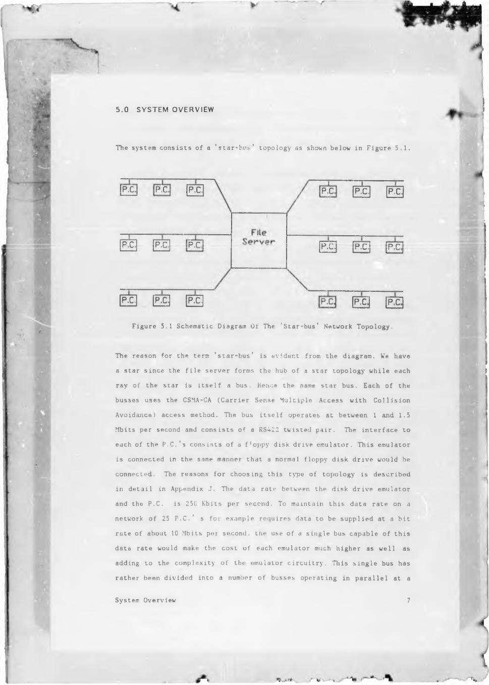
5 . 0 SYSTEM OVERVIEW
The system consists of a 'star-bvtv' topology as shown below in Figure 5.1.
P.C P.C P.C. P.C P.C. P.C.
P.C. P.C. P.C P.C. P.C. P.C
P.C. P.C. P.C. P.C P.C P.C
Figure 5.1 Schematic Diagram Of The 'Star-bus' Network Topology.
The reason for the term ’star-bus' is evident from the diagram. We have
a star since the file server forms the hub of a star topology while each
ray of the star is itself a bus. Hence the name star bus. Each of the
busses uses the CSMA-CA (Carrier Sense Multiple Access with Collision
Avoidance) access method. The bus itself operates at between 1 and 1.5
Mbits per second and consists of a RS422 twisted pair. The interface to
each of the P.C.'s consists of a floppy disk drive emulator. This emulator
is connected in the same manner that a normal floppy disk drive would be
connected. The reasons for choosing this type of topology is described
in detail in Appendix J . The data rate between the disk drive emulator
and the P.C. is 250 Kbits per second. To maintain this data rate on a
network of 25 P.C.' s for example requires data to be supplied at a bit
rate of about 10 Mbits per second, the use of a single bus capable of this
data rate would make the cost of each emulator much higher as well as
adding to the complexity of the emulator circuitry. This single bus has
rather been divided into a number of busses operating in parallel at a
System Overview 7

lower data rate. A substantial reduction in the cost per emulator can be
achieved but the complexity of the fiV-server hardware is increased.
This compromise was accepted however.
The network appears to the. P.C. on the hardware level as a floppy disk
drive unit and to the software as a number of logical floppy disk drives.
These additional logical disk drives are used by the file-server to pro
vide access to the software pool as well as individual user areas. The
data is transferred from the file server to the emulator in the form of
tracks of data rather than individual files. This requirement is a direct
result of the nature of the floppy disk emulator and will be explained
later.
The P.C. is provided with a type of menu program, the selections being
Lne software available for lhat particular operating system. One of these
menu programs would be required for each of the operating systems that
may be. used on the P.C. . When the P.C. 'boots-up' initially off the
network, the user would have to provide a user 1,1 . and password which
is used in the network management. The menu program loaded would be that
for ‘IS-DOS since this is the most frequently used operating system at this
stage. One of the options in this menu would be to change operating sys
tems. The menu program performs a fundamental role in the software pro
tection system since it is through this program that the user obtains
access to the protected software on the xile-seiver. The menu program
'maps-in' the requested software and hands ov< control to this software
package. When the package terminates, control is returned to the menu
program to 'map-out1 the software package. Hy doing this the user, even
if he leaves the menu program to the operating system, is unable to copy
any of the protected software since it will be mapped out of the system.
Problems do arise however in software packages that allow the use** to copy
files from within the package. Although elimination of the floppy disk
drives altogether from the P.C. would ensure that no copying took place,
System Overview 8

it was considered necessary that at 1 east one diive should be retained.
The reasoning behind this argument is that the students would be unable
to take any of their work home with them if they wished to do so.
An explanation of the operation of the entire system is rather complicated
and for this reason the explanation will start off with the simplest
configuration. This will be expanded upon until the full system is
reached.
The system developments that will be described are the following:-
1. One P.C. with the floppy disk drive emulator connected to the file-
server. The emulation of a single floppy disk will be described.
2. The same hardware configuration as in (1) but 2S floppy disk drives
will be emulated.
3. The operation of the menu program and software protection using the
same configuration as in (2).
4. The combination of a number of P.C.'s operating as in (3).
9
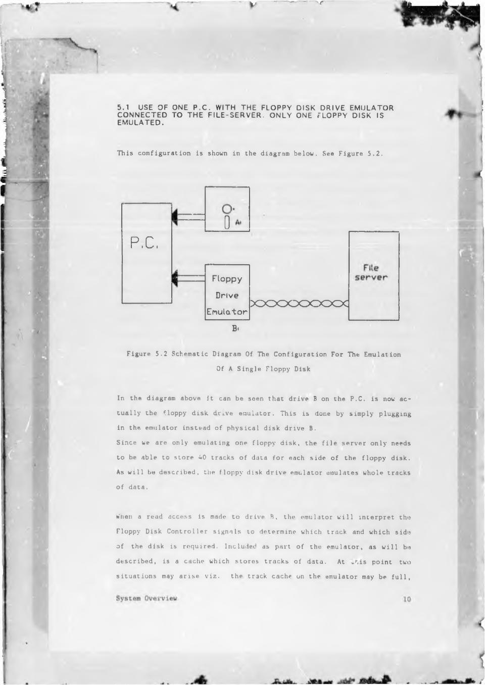
5.1 USE OF ONE P C . WITH THE FLOPPY D ISK D R IV E E M U LA T OR C O N N E C T E D TO T H E F IL E -S E R V E R . O N L Y ONE FLOPPY D ISK IS E M U L A T E D .
This configuration is shown in the diagram below. See Figure 5.2.
0P.C,
Floppy
Drive
EmulatorXDCOOOOOO<
B.
Figure 5.2 Schematic Diagram Of The Configuration For The Emulation
Of A Single Floppy Disk
In the diagram above it can be seen that drive B on the P.C. is now ac
tually the floppy disk dti.ve emulator. This is done by simply plugging
in the emulator instead of physical disk drive B .
Since we are only emulating one floppy disk, the file server only needs
to be able to store 40 tracks of data for each side of the floppy disk.
As will be described, the floppy disk drive emulator emulates whole tracks
of data.
When a read access is made to drive B, the emulator will interpret tho
Floppy Disk Controller signals to determine which track and which side
of the disk is required. Included as part of the emulator, as will bo
described, is a cache which stores tracks of data. At .r.is point two
situations may arise viz. the track cache on the emulator may be full,

or the cache may be empty or partly filled. In the latter case which will
occur most often when the emulator has just been powered up, the track
cache index will be searched to see if the required data is in the cache.
Obviously immediately after power-up the cache will be empty. In general
if the required data is found, the emulation process will commence imme
diately thus allowing the I loppy Disk Controller to begin reading in the
required data. When the required data is not found in the cache, a 're
quest' is sent to the. file-server for the required data. The file-*erver
then accesses the required data from its cache or disk and sends it to
the emulator. The emulator then updates its track cache and begins the
process described again.
When the track cache is full and the required data is not in the cache,
the cache management algorithm as will be described is implemented. This
algorithm decides which data in the cache should be over-written. The
process is then the same as described above viz. a request is sent to the
file-server and the data returned is then placed in the area that has just
been freed.
A write access to drive B is very similar to that described abcve for a
read access. The entire truck of data to which the write is taking place
still has to be emulated and thus the same procedure as above is followed.
When a track has been written to, this fact is flagged and the track
cannot be replaced in the cache until the updated version of the track
is written to the file server. This write takes place as soon as the em
ulator is able to access the file servar for this write operation.
The fact then that the data is not coming t rom a physical floppy disk
drive is totally invisible to the B.C. . The only modification that has
been made to the B.C. is the replacement of the physical disk drive by
the emulator.
System Overview 11
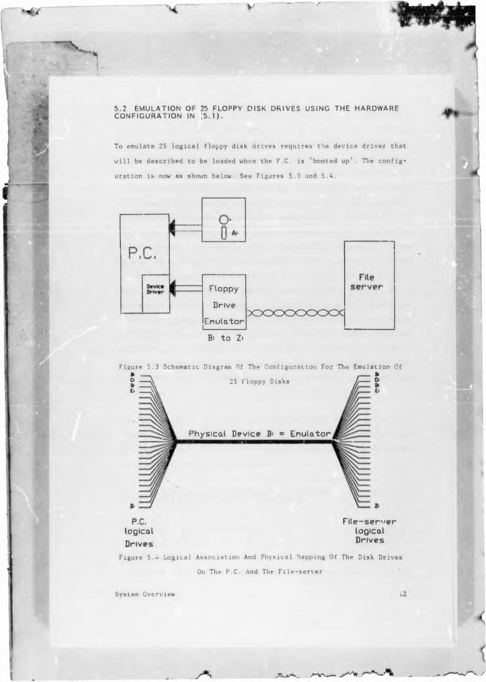
5 .2 E M U L A T IO N OF 25 FLOPPY D ISK D R IV E S US ING THE HARDWARE C O N F IG U R A T IO N IN [ 5 . 1 ) .
To emulate 25 logical floppy disk drives requires the device driver that
will be described to be loaded when the P.C. is 'booted up'. The config
uration is now as shown below. See Figures 5.3 and 5.4.
M Floppy
Drive
EmulatorX D O C X D C O O C X
B' to Zi
Figure 5.3 Schematic Diagram Of The Configuration For The Emulation Of» _________________________ ft{jj -- \ 25 Floppy Disks b--L ZZZa\ £•
Physical Device Bi ■ Em ulator
P.C.logicalDrives
F lle -s e rv e rlogicalDrives
Figure 5.4 Logical Association And Physical Mapping Of The Disk Drives
On The P.C. And The File-server
System Overview
As described in detail in Appendix M , the device driver performs some
'pre-processing' of the DOS calls for the floppy disks. This pre
processing consists of mapping all the logical disk drives from 3: to Z:
to one physical device viz. drive B. (Note MS-DOS assigns the logical
drives the letters of the alphabet from B to Z). This alone would be
rather pointless since we would still be accessing the same data no matter
which logical drive was selected. To overcome this a record is kept both
in the device driver and the floppy disk emulator as to which logical
device was accessed last. Whenever there is a change in the logical device
being accessed, a message' is sent to the emulator informing it of the
change. This message is sent to the emulator by writing a sector to track
40 which is beyond the normal range of track numbers used viz. 0 to 39.
Sending this message is vital since we may have track 1, say, of each of
the logical devices in the cache on the emulator and we must be able to
distinguish between which one is required. This write is performed using
one of the BIOS routines. The track emulator interprets this message and
all subsequent searches of the track cache index include this drive
identifier as one of the search criteria. The reason that track 40 is used
for message passing and the mechanism used in message passing is described
in Appendix L.
The user would then be able to access in effect 26 floppy disks. This
includes his physical drive A along with 25 floppy disks of data on the
file-sorver. Any of this data is accessible in the same way Lz data would
be accessed from any other disk drive.
5 .3 THE O PERA TION OF THE MENU PROGRAM AND SOFTWARE PR O T E C T IO N ON THE SYSTEM D E S C R IB E D IN ( 5 . 2 ) ABOVE.
The operation of the menu program is vital in the attempt to prevent
unauthorised software copying. The idea itself is rather simple. When he
user 'boots-up' the computer the first menu program will automatically
he executed. This menu will be that of the programs available that use
Syttern Overview 13
/-"VS—

the MS-DOS operating system. This program then prompts the user for his
choice. When a choice is made the file server is notified of the requested
software. The file-server then associates virtual floppy disks in its mass
storage with as many disks us the package requires. The current drive is
changed to whichever drive the package is on. The program is then loaded
and executed using the normal DOS call. This commences with a directory
search for the file-name The directory was empty previously but now it
contains the require i file-name.
An example may be useful to further illustrate the system. Consider a user
that boots up the computer and is provided with the menu choice, He then
branches from the menu to the operating system level. If the user now asks
for a directory of any of the logical drives on the file server, the re
sponse will indicate that there are no files on any of these drives. He
is unable then to copy any software.
Assuming the user returns to the menu program and requests a program
called 1Gamma-graphix' for example. This package when normally run on
floppy disks occupies three disks. The menu program then maps this package
into drives B , C and D say. At this stage if the user was able to exit
to the operating system and ask for a directory of drives B, C or D he
would find all the files on these disks that would normally be on the
individual floppy disks. (He would then bv able to copy these files). The
menu program would then commence execution of Ramma-graphix. When the user
exits from Gamma-grnnhix whether normally or abnormally, the menu program
would map Gamma-graphix out of drives B, C and 0. If the user now gets a
directory of these drives they would indicate that there are no files
present.
When a software package is requested in the menu program, a message is
passed to the disk emulator in the same way as in (2) above. The infor
mation contained in such a message is different however. The message
content in this case would include the number of floppy disks the package
System Overview 14

requires as well as in 'application number1. These messages are forwarded
directly to the file-se vf". Each application package has an application
number that has an important role in the overall system. For example when
the file-server maps out a software package a number of tracks of that
package will probably be present in the disk drive emulator track cache.
We could remove these U auks from the cache though it would be more ef
ficient to leave them there so that if the user left package A and then
decided soon after that he was going to use package A again, the tr .cks
of package A still in the cache would not have to be re-transferred across
the network.
The application number becomes an added search criterion when the track
cache index is being scanned to find a particular entry. The present ap
plication number being used is stored in the floppy disk drive emulator
and is updated each time the menu program writes a message to the emula
tor.
The menu program would then provide a degree of software protection by
not allowing the user to have direct access to the software files.
L .4 A NUMBER OF P . C . ' S O P ER A TIN G AS IN ( 5 . 3 ) ABOVE.
Extending the above system to a number of P.C.'s does not require much
effort at all. The only requirements now are that the user is prompted
for a user I.D. and password when the P.C. is booted up initially. Each
P.C. has associated with it a particular node number. The user I.D. pro
vides a logic i1 link to each user for the fi le-server while the node
number provides a means for the network software to know where exactly
to send the data. The network software also now has to contend for the
network since the emulator fi le-server link is now shared by more than
one user.

6 . 0 THE FLOPPY DISK D R IVE EMULATOR
Up until now reference has been iruue to the floppy disk drive emulator
that provides the interface between the P.C. and the network. Natural ly
a few questions arise viz. What is this floppy disk drive emulator, how
does it work and why emulate a floppy disk drive at all. These questions
will now be answered.
Firstly, what is a floppy disk drive emulator? The disk drive emulator
is a piece of microprocessor based circuitry that is able to emulate the
characteristics of a floppy disk drive unit. Operation of the emulator
will be discussed in detail later. The most interesting aspect is why
emulate a floppy disk drive. If we look at microprocessor systems over
recent years we soon see that the floppy disk has been the fundamental
means of transferring data between these machines since they are in effect
removable mass storage media. To execute a number of software packages
on a P.C. for example we would load these packages from a number of floppy
disks. The driving force behind the floppy disk drive emulator idea as
the connection to the network is tha instead of physically loading sep
arate floppy disks, the network could provide the same data, that would
be stored on u central file-server, to a floppy disk drive emu 1a10/. The
P.C. is then totally unaware that the data is coming from a network and
not from separate floppy disks. To appreciate why the floppy disk drive
itself should be emulated we must examine the whole disk system of a P.C..
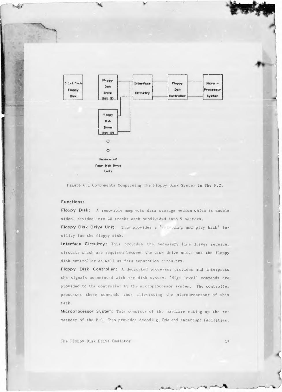
Components Compris ing the Floppy Disk System in a P .C . The primary
components of the floppy disk system in a P.C. arc identified and their
functions and structure described. The components are shown in Figure 6.1.
The Floppy Disk Drive Emulator 16
Floppy
Disk
F loppy
Disk3 1 /4 Inch F loppy
Disk
o
oMcurtmjn o f
Fovr- Disk D rive
U n its
Figure 6.1 Components Comprising The Floppy Disk System In The P.C.
Functions:
Floppy D isk: A removable magnetic data storage medium which is double
sided, divided into 40 tracks each subdivided into 1 sectors.
Floppy Disk D r ive U nit: This provides a *r ding and play back' fa
cility for the floppy disk.
In te r fa ce C i r c u i t r y : This provides the necessary line driver receiver
circuits which are required between the disk drive units and the floppy
disk controller as well as data separation circuitry.
Floppy Disk C o n tro lle r : A dedicated processor provides and interprets
the signals associated with the disk system. 'High level' commands are
provided to the controller by the microprocessor system. The controller
processes these commands thus alleviating the microprocessor of this
task.
Microprocessor System: This consists of the hardware making up the re
mainder of the P.C. This provides decoding. DMA and interrupt facilities.
The Floppy Disk Drive Emulator 17

The BIOS (Basic Input/Output Subroutines) provides low level software for
the floppy disk system (among other things).
From the above description we can see that only two components may be
emulated viz. the floppy disk drive nnit an^ the floppy disk controller.
When we consider the inputs and outputs and complexity of emulation of
each of these devices, emulation of the floppy disk drive unit is more
favourable.
From the diagram we can see that the floppy disk controller is interfaced
directly to the microprocessor system. This requires that the controller
be emulated on both the hardware and software levels. As described in
Appendix C the floppy disk controller is a very complex device. From a
purely practical point of view emulation of the controller would require
in a number of situations that the component be unsoldered from a circuit
and be replaced with a plug in header, say, thst is connected to the em
ulation circuitry. From an installation point of view the user would have
a daunting task on his honns.
Emulation of the floppy disk drive unit is restricted to hardware emu
lation. The number of inputs and outputs to the emulator is much smaller.
A disadvantage of this system, however, is that it is not possible to
identify which sector is required by the floppy disk controller. It is
only possible to isolate which track and which side of the disk is re
quired. See Appendices B and C .
An alternative to emulating both tin* floppy disk controller as well as
the floppy disk drive is the design and construction of a plug-in board
for the P.C.. This is the form that most of the commercially available
network boards take. These boards can interfere with the DMA and interrupt
system on the I’.C. (e.g. the same interrupt used by more than one board,
the same I/O addresses may he used etc.). Extensive software is often also
The Floppy Disk Drive Emulator 18
required to drive them. This software can often cause problems when dif
ferent operating systems are used with the same network card and may even
be problematic with everyday software packages. In this respect emulation
of the floppy disk drive unit does not interfere with DMA, interrupts or
the software since we rAn virtually say that the software is un-modificd.
The MS-DOS device driver for the extra logical drives is virtually iden
tical to that for the normal disk drive system. The only exception is the
message passing to track 40 but even this is totally transparent to
MS-DOS.
System busses into which plug-in boards are inserted and floppy disk
controllers are very specific devices. Emulation of the disk drive unit
is less specific since a number of disk drives have the same interface.
The small discrepancies that may occur can be overcome by adapting the
emulation principles developed. With speculation that future P.C.'s will
be equipped with 34 inch drives makes emulation of the disk drive a log
ical step. Current specifications for 3j inch devices indicate that the
emulator can be used, with possibly some small software modification on
these systems (2).
By keeping the P.C. interface as we would by emuliting the disk drive it
would be possible to include P.C.'s of various makes on the same network.
If these P.C.'s share the same operating system as other makes of machine
on the samv network, it would be possible for files to be shared by these
machines. This would be more difficult if a plug in card were used, say,
since these cards would have to be tailored to the individual systems.
C . l THE FLOPPY DISK D R IV E EMULATOR (HARDWARE)
The floppy disk drive emulator can be divided into six sub-sections.
These sections are:-
1. A decoder to process data being written to the disk drive.
The Floppy Disk Drive Emulator 19

2. An encoder to reproduce data being read from the disk drive.
3. A track counter to monitor the required head movement.
A. The CPU, RAM and EPROM to control the emulator and provide the track cache.
5. The network interface.
6. The interface to the floppy disk drive interface.
As described in Appendix D the date recorded on the floppy disk is MFM
encoded. If the fact that the data is MFM encoded is disregarded for the
moment and the data format on the floppy disk as described in Appendix A
is considered, the following characteristics become apparent:
1. The data stream is very similar to that on a synchronous communi
cations link.
2. The data is divided into blocks on which Cyclic Redundancy Checks
(CRC) are calculated.
Considering these two observations a synchronous communications device
was chosen to perform these tasks. Using NRZ (Non Return-to-Zero) encoding
on this communications chip the data entering and leaving the emulator
would just require MFM decoding and encoding respectively. The data flow
is shown in Figure 6.2.
VD and RD are the data input and output to the floppy disk drive units.
The lines shown here are the same as those on the 34 way interface cable
(See Appendix H ) except they have a1 ready been buffered.
This is conceptual ly how the data i low is managed. Unfortunately the
implementation is not quite so simple. The full details of these sub
sections are given in Appendices E and F .
The Floppy Disk Drive Emulator 20
_____ .. v6uA-
It is ne-essary to monitor the head position so that the correct track
can be emulated when required. The required head movement is indicated
to the floppy disk drive by two lines. These lines, DIRection and STEF,
convey this information. The state of the DIR line determines whether the
head must move inwards or outwards. Each pulse on the step line represents
the movement to move from one track to the next.
SynchronousCommunications
MFMEncoder
MFMDecoder
TxD
RxD
ChipHeon Brt R ate of ESOKbrts p e r second
Figure b .2 Flow Of Data In And Out Of The Emulator
For the floppy disk controller to know where the head is immediately after
power-up, for example, a feedback signal is provided from the floppy disk
drive unit to the disk controller. This signal, TRACKO, indicates that
the head is positioned over track 0 (the outermost track of the disk).
The floppy disk controller, when issued with a Recalibrate command (3),
steps the head outwards until the TRACKO signal becomes active. The floppy
disk drive controller then sets its internal counter to zero.
The Floppy Disk Drive Emulator 21
The principle of the floppy disk controller's track control circuitry is
extended to the emulator. An up-down counter whose direction is controlled
by DIR and clocked by STEP performs this function. The outputs are gated
to provide the TRACKO signal when the counter's value is zero. The outputs
are also made available to an input port on the CPU controller so that
the counter can be monitored.
The track counter is shown below in Figure 6.3.
Up/Down— Dato Bus
U L E Counter
OR
TRACKO
Figure 6.3 Schematic Diagram Of The Emulator Track Counter
The entire functioning of the emulator is co-ordinated using a micro
processor based system, the central processing unit used is the INTEL
80168. This is supported by 256Kbytes of RAM, (expandable to approximately
1Mbyte), SKbytes of EPROM, 2 Z8530 Synchronous Communications Control
lers, an 8 bit input and an 8 bit output port.
The 80188 CPU is ideal in this application since it combines a number of
peripheral devices within one physically small component. A dual channel
DMA controller, 3 16 bit timers, an interrupt controller, bus controller,
The Floppy Disk Drive Emulator 22

chip select logic, ready generation logic as well as a clock generator
are included in the package. 1 Mbyte of memory as directly addressable
which is extremely useful for cache management. The timer, clock gener
ator and DMA unit are used to overcome the problems commonly associated
with dynamic RAM memory. See Appvr.dix II. In the pn?sent implementation
of the emulator only ZSoKbytes of RAM are used. The emulation software
and general 'house-keeping' software resides in the Ei'ROM. The two Syn
chronous Communications Controllers (SCO are used for the emulator and
network. As mentioned above the input port is required for the track
counter. An output port is provided to drive L.E.D.'s to indicate various
states on the emulator and for general diagnostic purposes. The SCC's
provide various other control inputs and outputs that arc required.
The network interface consists of direct transmission of the data clock
along with the data on a three line system between the nodes. The only
additional circuitry required on the SCC's are the RS422 line drivers and
receivers. The line drivers outputs are controlled by the ITS line of the
network SCC.
Circuitry is required to interface the emulator to the floppy disk drive
interface circuitry. This circuitry is based on an open collector bus type
of system. All the outputs o f the emulator have to be equipped with open
collector drivers while the inputs must only accept information on the
bus when the relevant physical drive is selected. See Appendix G. The
circuitry is simple, however, ind merely coisists of latches and pull up
resistois on the inputs and open collector drivers on the outputs.
6 .2 THE FLOPPY DISK D R IVE EMULATOR (SOFTWARE)
Thy first aspect of the emulation software that will be discussed is that
of the track cache. An urea oi RAM memory <10LK) in this case has been
set aside for creating such a each* .
The Floppy Disk Drive Emulator 23

An index of the cache contents is kept separate from the data area of the
cache. This index contains entries identifying the track number, the head
number (i.e. side of the disk), the application number counters for the
implementation of the caching algoi.'hm and o pointer to the actual data
, The function of the track, liedu and application number has been
explained in the system overview. When the cache is full, a caching al
gorithm is implemented to determine which track entry should be replaced.
The algorithm is based on a method where both the frequency of access as
well as when last an entry was accessed are used in the decision algo
rithm. This decision algorithm is particularly well suited to small sized
caches. A detailed explanation of both the cache and the replacement al
gorithm is given in Appendix I.
Important aspects of the flow-chart will be mentioned here. See Figure
6.4.
The hardware of the emulator needs to be initialised and the memoiy tested
before the emulation process can be started. The CPU itself needs to have
certain parameters set up before the rest of the software can be executed.
Memory and I/O mapping as well as 'wait-state" generation are of primary
importance. One of th three timers as well as one ol the DMA channels
need to be configured to commence the refreshing of the emulator's dynamic
RAM. DMA cycles are performed at fixed time intervals to carry out this
function. Faulty memory locations are located by writing known bit pat
terns to an area of memory and than reading the contents of this area and
checking for correspondence. If all the memory functions as required the
truck cache is initialised. The current disk and application numbers are
given values that would not exist under normal circumstances and this
ensures that when the cache index is searched, the search fails and the
data is requested from the file server.
The Floppy Disk Drive Emulator 24
Initialisation
Read Track Counter Value
Read Head Value
emulate Track 40 Side 0, Sector 1Track 40 ?
INQ Get Current Drive and Appln. Nos.
Search Cache
Reqd Track Found 7
Apply Replacement Algorithm
Walt For Data
Insert Data In Cache
The Floppy Disk Drive Emulator 25
Figu
re
6.4
Flo
w-c
har
t Of
Th
e E
mul
ator
S
oft
wa
re

The track counter value is read from the Input port. One of the control
inputs on the SCC is used to check which head is required. This is pos
sible since the head can be only one of two values viz 0 or 1. If the
track counter value is y it is immediately identified with the ex
ceptional case of a message being passed to the emulator and an abnormal
track emulation takes place. The track size is reduced to 1 sector and
only track 40, side 0, sector 1 is emulated. This is done primarily to
save time as emulation of any further sectors is a waste of time The
message is then read in. This is done in the same way as any normal sector
write except that the is not written into the cache. Processing the
message may simply involve updating variables on the emulator such as the
current drive number and/or application number, sending an application
request to the file server or both.
If the track counter value read is between 0 and 39 then using the stored
drive and application numbers, the track index is searched to find an
entry corresponding to the required trcck and side as well as the correct
drive and application number. If the required entry is found, a pointer
to the data area is returned and the track emulation process is initiated.
The variables for cache management are also updated. In the case of an
entry not being found the cache replacement algorithm comes into effect.
The entry used least frequently is replaced. If the situation arises where
two or more entries have the same frequency of use the one that hasn't
been used for the longest period of time. This algorithm is desv^ibod
in detail in Appendix I. Once the area of the cache that is to be over
written has beet identified a message which includes information which
identifies the requesting vmulaior (source address), the typv of message
(request lor data), the required drive, application, track and side num
bers, is sent to the file server. The actual access method on the network
(CSMA-CA) is described in Appendix K . This method was chosen for its ease
of implementation both in ie*-ms of hardware and software. With the small
The Floppy Disk Drive Emulator 2b

number of users on each of the buss' < as explained in Appendix J (+- 5
users per bus), each user should receive sufficient use of tho network.
When the data is returned from the f i Iv-sewer it is inserted into the
track cache. The main emulation software is then called. As is explained
in Appendix P, the track emulation begins with the generation of the index
pulse followed by the gap preceding the first sector. Before each sector
is emulated the track number a-, well as the side number is re-read from
the respective input ports so that as soon as the floppy disk controller
has performed the required ^unction on the track initially chosen, the
emulator can respond to any change in the requested track or side. Con
tinued emulation of the originally chosen track is a waste. Emulation
of a particular track continues therefore until there is a change in the
emulator track or side inputs. The formatting information between sectors
has been reduced to the minimum possible so that as much emulation time
as possible is devoted to emulating data rather than formatting informa
tion that is useless to the user.
The Floppy Disk Drive Emulator 27
7 .0 REQUIREMENTS OF THE F IL E -S E R V E R
The requirements of the file-server both in terms of hardware and software
are discussed.
From a high level point of view the file-server has to manage the access
of a number of users both to an area of common software as well as the
individual user areas. The file-server software is closely associated
with the menu program on the P C. and the finer details of both their
implementations are beyond the scope of this report. In general though
the menu program instructs the file-scrv associate a certain number
of floppy disks with logical disks on tl . . Upon a request from the
P.C. the file-server must bt>. capable of providing any track required from
one of these logical disks. T1 perating system on the P.C. is always
in control of the logical disks themselves thus allowing the operating
system on the tile-server to be- different from that on the P.C. It would
be an advantage if the file-server used a multi-tasking operating system
so that disk accesses for example can be taking place at the same time
as other processing tasks. The file-server requires extensive mass stor
age facilities, the access time of which is of xtreme importance. In tnis
regard the. implementation 01 a track cache on the file-server would reduce
the access times particularly for software that is access by a number of
users.
The lower levels of software are dependant on the type of hardware
interface that exists between the file-server and the network. The two
situations that can be defined her.; are the cases uhere the processor
controlling the file-server controls the network, and then the case where
the network is controlled by a separate processor. In the latter case
communication with the network is by means of messages passed between the
processors. In the first case the hardware of the file-server needs a
synchronous communications port capable of handling SDLC communications
Requirements of the File-server 28

at speeds between 1 and l.SMbits per second. Software also has to imple
mented to control the media access. This makes the use of a multi-tasking
operating system virtually obligatory.
The second approach involves the inclusion in a multiprocessor environ
ment of a processor to handle the network management ""d media access.
Communication between the network processor and file-server processor is
by means of two queues. Requests from the network are entered into the
input queue while data for the network is extracted from an output queue.
These queues would be maintained in a memory area that can be accessed
by both processors. Tran, the fill-server's point of vi<*u communication
with the network would consist of fetching requests from the input queue,
processing them and providing the results in the output queue. This re
lieves the file-server of a large amount of processing.
The proposed system dees not therefore pose any major constraints on the
capacity, make of, or operating system used, on the file-server.
Requirements of the File-server 29

8.0 C O NCLUSION
A set of network requirements for an educational environment were derived
after analysing the requirements and peculiarities of such a system.
The proposed system , based on a 1star-bus' topology, provides a low
cost, flexible system. The file-server which forms the hub of the star
topology is subject to no major constraints and can be of any make and
use any operating system but should have mass storage facilities with
access times that are as short as possible. Using an RS422 twisted
pair bus provides a medium speed link at between 1 and 1.5 Mbits per
second as well as being cheaper, in terms of both material and in
stallation costs, when compared with a coaxial cable based system. The
CSMA CA access method provides a simple yet effective means for
controlling each of the busses especially since the number of users
per bus is small. No sophisticated hardware or software is requirea to
implement it either. The use of a radio based system on one or more rays
of the star for connecting computers that are some distance from the
file-server should be investigated since the CSMA CA access method does
lend itself to this type of medium as well.
The use of a floppy disk drive emulator as the interface between the P.C.
and the network is certainly a new approach. This method eliminates most
of the hardware incompatibilities that are often associated with plug-in
network boards as well as dispensing with the need for operating
system modifications. The design, implementation and testing of such
a unit has been described. Certain constraints laid down in the network
requirements have been satisfied by this interface. The cost of the
interface is approximately the same as that of a typical floppy disk
drive unit. No components have been used that are rare or expensive.
Most of the components can be ou ained from more than one man
ufacturer . The performance of the disk drive emulator unit when tested
Conclusion 30
as a stand alone unit proved to be excellent. Response time was
within the requirements and no data errors were encountered during the
testing.
Two disadvantages of the system must be mentioned. Due to the structure
of the network and the P.C. interface, the nett data rate between the
emulator and the P.C. is 250Kbits per second. When a single user,
therefore, is using the system he will not receive the full benefit
from the network operating at 1.SMbits per second, say, due to the
lower transfer rate between the emulator and the P.C.. The second
matter is not really a disadvantage but should be considered for
optimal performance. Since the data is transferred between the file*
server and the emulator in the form of tracks, the files should be
kept in a form that all the sectors on the tracks transferred ac
tually carry useful data. This can be ensured by keeping the. files on
the file-server in a contiguous form.
A limiting factor of the system under heavy loading could be the data
transfer rate between the file-server hardware and the file- server mass
storage system. This would limit the amount of data availaole to the
network. A cache in the memory of the file- server could reduce this
limitation in situations were the loading is heavy but a number of
users are requesting the same software.
These last two limitations should not make the overall system less
attractive. To ensure that the requirements laid down are met further
research and testing is required on the file-server and the network it
self. The performance of the file-server is very important since all the
data being transferred on the network passes into or out off it. Con
nection of a single floppy disk drive emulator to the file server will
give a good idea of the best performance possible. Extending the testing
to a full complement of P.C.'s on a ray of the star will give a good in
Conclusion 31

dication of the overall performance of the system since any additional
rays added will he operating in effect in parallel. The file-servers ca
pabilities will be the limiting factor. Implementation of a printer and/or
a plotter server using the message passing mechanism on track 40, as de
scribed, should be investigated. These servers will have to use other
tracks though.
The research described in this dissertation has described the network
system in general terms and the P.C. interlace in detail. It has also
provided a number of aspects that should be researched to optimise the
performance of the network as a whole.
Conclusion 32
APPENDIX A THE STRUCTURE OF FLOPPY DISKS
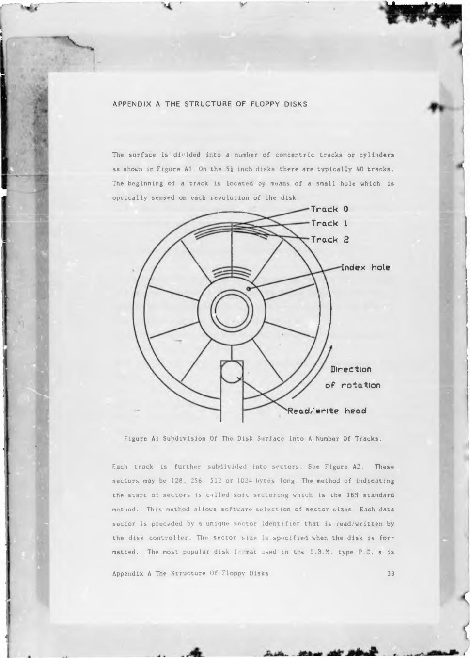
The surface is divided into a number of concentric tracks or cylinders
as shown in Figure A1 On the 5j inch disks there are typically 40 tracks.
The beginning of a track is located by means of a small hole which is
optically sensed on each revolution of the disk.Track 0 Track 1Track 2
index hole
Directionof rotation
Read/write head
Figure A1 Subdivision Of The Disk Surface Into A Number Of Tracks.
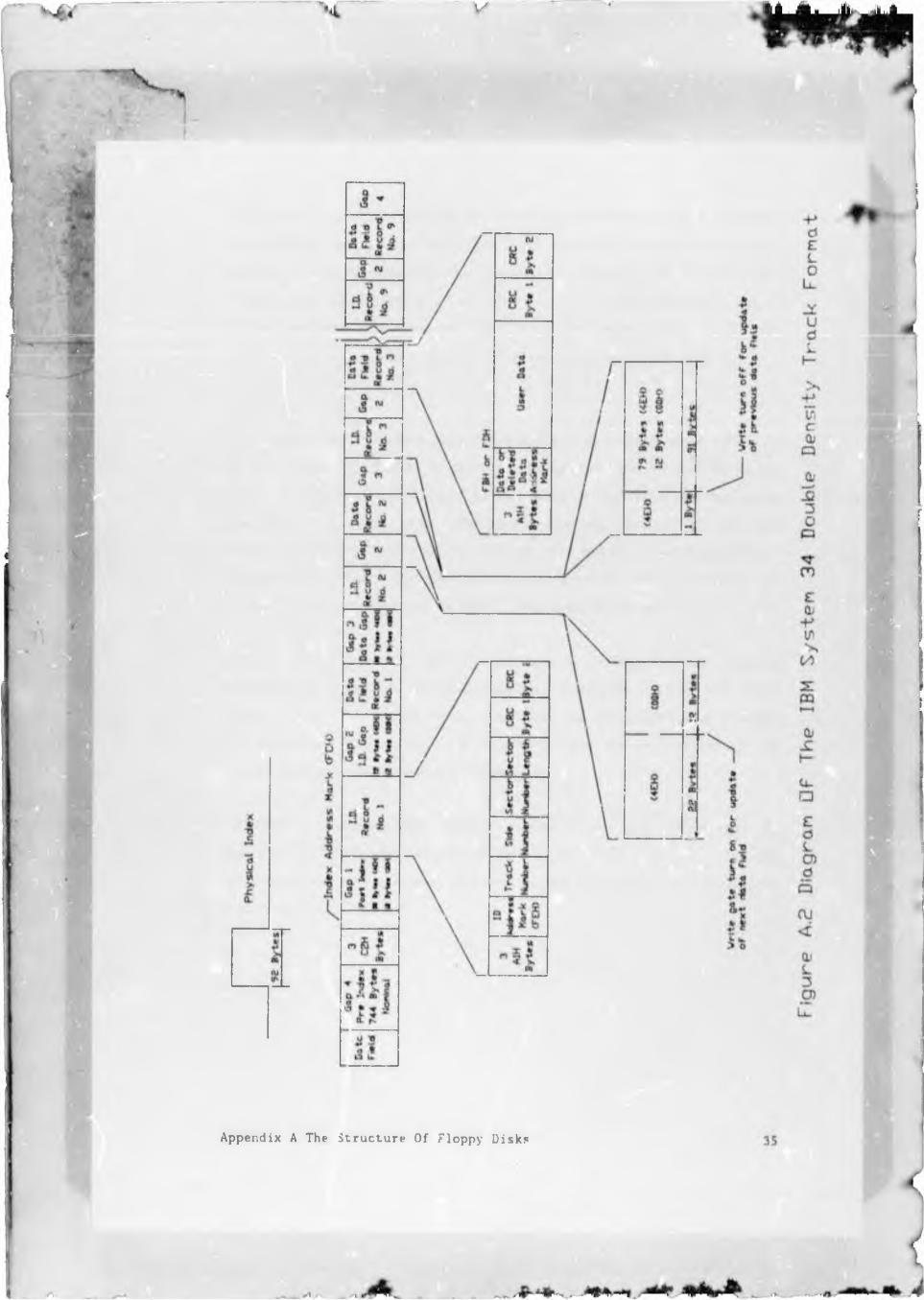
Each track is further subdivided into sectors. See Figure A2. These
sectors may be 128, 256, 512 or 1024 bytes long. The method of indicating
the start of sectors is called soft sectoring which is the IBM standard
method. This method allows software selection of sector sizes. Each data
sector is preceded by a unique sector identifier that is read/written by
the disk controller. The sector size is specified when the disk is for
matted. The most popular disk T mat used in the I.B.M. type P.C.'s is
Appendix A The Structure Of Floppy Disks 33

the 360K format. These disks are double sided which means there is a
read/write head on either side of the disk. The disks rotate at 300 r.p.m
which gives a rotation time of 200ms.
The 3t>0 Kbyte capacity is achieved as follows:-
The disk is subdivided into 40 tracks which arc then further subdivided
into 9 sectors each with 512 bytea. (l/2Kbyte). (Note this applies to
MS-DOS version 2 and subsequent versions). This gives a total of * X 40
X 9 = 180K. This is the capacity of each side of the disk and since the
disk is double sided the total is 360K.
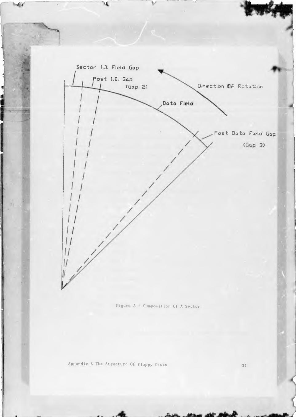
Each .ector is composed of four fields. See Figure \3.
1) The Sector I D. Field. This is ten bytes long and is written only when
the disk is formatted. This provides the sector identification that in
used by the controller when data is read fr.m or written to the disk.
The ten bytes each hive the following functions:
Bytes 1 - 3 are A1H bytes with missing clock pulses. These form part of
the address marker. See Appendix D.
Byte 4 - l.D. Address marker. This specifies the beginning of the l.D.
field.
Byte 5 - Track (cylinder) address
Byte 6 - Head address
Byte 7 - Sector address
Byte 8 - Sector length code
Bytes 9 and 10 - This is a 16 bit CRC for the l.D. field calculated on
the first eight byt"«.
The controller supplies the address mark during formatting and the three
preceding A1H bytes. The rest is supplied by the processor software.
Appendix A The Structure Of Floppy Disks 34
Appendix A The Structure Of floppy Disks

2) The Post ID. Field Gap (Gap 2). This gap is written during formatting.
During write operations, the device write circuitry is enat led within the
gap and are re-written each time a sector is updated. During read oper
ations the trailing bytes of the gap i.e. the 12 00H bytes are used to
synchronise the data separator Ionic with the upcoming data field. The
i umainder of the gap consists of 4EH bytes as shown in the Figure.
3) The Data Field
This field also commences with 3 Alh byt»s with missing clock pulses as
in the sector I D. field. In this case though they are followed by an FBH
byte. If the data area is found to be faulty during the format operation
the FBH byte is replaced by a FD1I byte indicating a bad sector. The rest
of the field is filled with the required data and has a two byte CRC for
the whole data field appended at the end (Note The CRC calculation in
cludes everything from and including the thro.' AIM bytes).
4) Post Data Field Gap (Gap 3). This gap is written when the track is
formatted and separates the proceeding data field from the next I.D. field
on the track This gap is not written alter the last sector on the track.
The number of bytes in this gap is programmable and is 22 bytes of 4EH
and 12 byi.cs of OOH as shown in Figure A2.
The CRC'c calculated above are calculated on t le most significant bit
first of each byte. The polynomial used is x1 * + x 11 + x1 + 1. The CRC
generators and receIvors trust be preset to all l’s before the calculations
are started.
Appendix A The Structure Of Floppy Disks 36
Sector I.D. Field GapPost I.D. Gap
(Gap 2) Direction Of Rotation
Post Data Field Ga
Figun- A.j Composition Of A Sector
Appendix A The Structure Of Floppy Disks 37
APPENDIX B THE FLOPPY DISK DRIVE INTERFACE
The interface to the floppy ilisk drive unit consists of a 34 way connector
cable. The odd numbered pins of this cable are grounded (i.e. pins 1 -
33). The remaining lines carry input and output signals at standard TTL
levels.
Output lines: These lines are driven by standard open collector gates. The
diskett" drives provide the pull-up resistors for these 1ines
Input lines: Each input line presents one low power Schottky (LO) load to t
diskette drives connected to the interface and is terminated
with a 150 Ohm load resistor to +5 V.
The even numbered lines have the following functions:
2,4,6,34 : No connection
8 : Index
10 : Motor 0
12 : Select 1
14 : Select 0
16 : Motor 1
18 : Direction
20 : Step
22 : Write Data
24 : Write Enable
26 : TRO (Track 0)
28 : Write Protect
30 : Read Data
32 : Hdsel I Head select)
In the following table 0 denotes an output while 1 denotes an input from
the P.C.'s point of vie',.
Appendix B The Floppy Disk Drive Interface 38
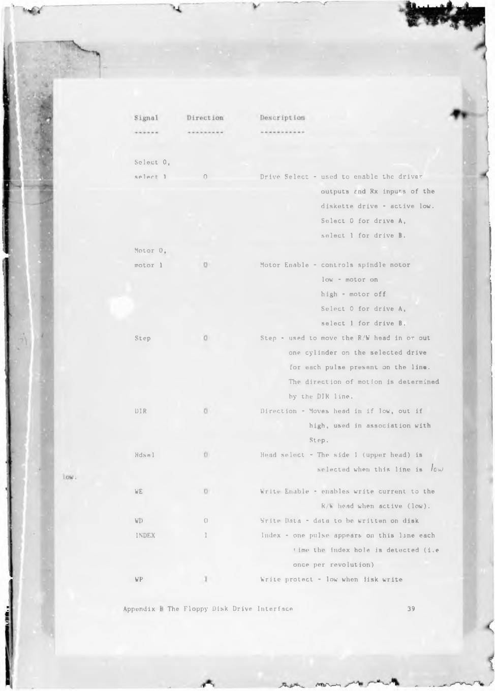
Select
s e l e c t
Motor 0
motor 1
Step
UIR
Hdse 1
WE
VI)
INDEX
WP
Appendix
0,
1 0 Drive Select - used to enable the driver
outputs end Rx inputs of the
diskette drive - active low.
Select 0 for drive A,
select 1 for drive B.
0
I
Motor Enable - controls spindle motor
low - motor on
high - motor off
Select 0 for drive A,
select 1 for drive B.
Step • used to move the R/W head in or out
one cylinder on the selected drive
for each pulse present on the line.
The direction of motion is determined
by the DIR line.
Direction - Moves head in if low, out if
high, used in association with
Step.
Head select - The side 1 (upper head) is
selected when this line is /oU
Ur ill- Enable - enables write current to the
R/U head when active (low).
Write Data - data to be vritten on disk
Index - one pulse appears on this line each
' ime the index hole is detected (i.e
once per revolution)
Write protect - low when lisk write
The Floppy Disk Drive Interface 39
.MVw-,
Signal Direction Description
Select
S P 1PCt
Motor 0
motor 1
Step
DIR
Hdsel
WE
VD
INDEX
WP
Appendix B
0,
1 0 Drive Select - used to enable the driver
outputs and Rx inputs of the
diskette drive - active low.
Select 0 for drive A,
select i for drive B.
Motor Enable - controls spindle motor
low - motor on
high - motor off
Select 0 for drive A,
select 1 for drive B .
Step - used to move the R/W head in or out
one cylinder on the selected drive
for each pulse present on the line.
The direction of motion is determined
by the DIR line.
Direction - Moves head in it low, out if
high, used in association with
Step.
Head select - The side 1 (upper head") is
selected when this line is IcU
0
I
Write Enable - enables write current to the
R/W head when active (low).
Writ*' Data - data to be written on disk
Index - one pulse appears on this line each
time the index hole is detected (i.e
once per revolution)
Write protect - low when disk write
The Floppy Disk Drive Interface
* * * * * *

protected
iRO I Track 00 - low when head over track 0
Read Data I Data read froiu the disk (data with imbedded
clock information)
Appendix B The Floppy Disk Drive Interface 40
APPENDIX C THE FLOPPY DISK CONTROLLER
The Floppy Disk Controller (F.D.C.) used in the l.B.M. type P.C.'s is the
Intel 8272A and the NEC 765. These LSI devices are very complex and will
only be described very briefly here. The F.D.C. interfaces to the central
processing unit like most peripheral devices and makes full use of the
interrupt and DMA resources available. The microprocessor is able to issue
15 'high level' commands to the F.D.C. These include read data, write
data, format a track, read a track, seek, recalibrate, sense drive status
etc. Typical parameters that are included with these commands are the
cylinder number (track number), head number, sector number, number of data
bytes in a sector, the last sector number on a track, the length of gap
3 etc.
Explanation of two of these commands will illustrate the functioning of
the F.D.C.
Firstly the seek command. This command is issued before data is read from
or written to a particular track. Although the cylinder number is one of
the parameters included in the read or write command, the floppy disk
controller does not automatically position the head over the required
track. The seek command is therefore necessary to perform this function.
When the seek command is issued the requested cylinder (track) number is
compared to the value stored in the controller. Step pulses on the STEP
line and the required level on the 1)1H line are asserted to position the
head over the required track.
When a urite command is issued, the F.D.C. begins to read the data passing
the read/write head. This continues until the required sector I.D . field
i.e. the sector I.D. field containing the required .ccior number is found.
As is shown in Figure A2 in Appendix A the synchronisation 00's are re
written followed by the data for the sector as well as the first byte of
Appendix C The Floppy Disk Controller 41

the next gap. These synchronisation bytes are rewritten each time a sector
is rewritten so that when the sector is read, the floppy disk controller
is properly synchronised with the incoming data field bv the time the data
field is encountered.
Appendix C The Floppy Disk Controller 42
APPENDIX D DATA RECORDING TECHNIQUES
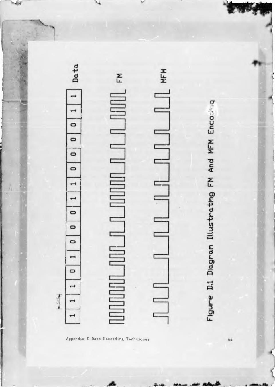
The recording technique used on a floppy - disk has to be such that it
is capable of conveying data as well as clock information. The method used
in double density recording as used on the P.C.'s under consideration is
called MFM (Modified FM). FM is the technique used in single density re
cording systems. The FM technique will be described first and then the
modifications will bo discussed.
Each data bit can be considered to have a 'bit cell1 associated with it.
In the FM technique, a pulse is always present at the beginning of each
bit cell (except for markers See later). This conveys the clock which
is used by the floppy - disk controller circuitry to synchronise itself
so that the data can be road correctly. If the data bit associated with
a bit cell is a 1, another pulse is present in the middle of the bit cell
i.e. there are two pulses in the bit cell. A 0 is therefore identified
by the absence of a pulse in the middle of the bit cell.
In the MFM technique, the pulse at the beginning of the bit cell NEED NOT
be present. The data bits are, as above, indicated by the presence or
absence at the middle of the bit cell for a 1 or 0 bit respectively. When
a 1 is followed by two or more 0 bits, the clock pulses at the start of
the bit cell ate re - inserted. This is necessary to maintain
synchronisation.
If we consider a bit call s i /.<• of ^ps as encountered on the standard 5i
inch floppy - disk interface, we can see ch<> waveform structure after
encoding in Figure 1)1. As can be seen, 3 fundamental time pacings between
pulses become ev e.nt. 4vis gaps are present between consecutive 1 bits
and between 0 bits after the second 0 hit rys gaps occur when there are
01 or 10 bit combinations except for the case of 101 where the gap is
Bps.
Appendix D Data Recording Techniques 43
Appendix D Data Recording Techniques
The difference between single and double density is clearly evident in
the figure The bit cell in the single density case is twice the size of
that in the double density name. The data per second ratio is therefore
2:1 between the two systems, .:ence the names.
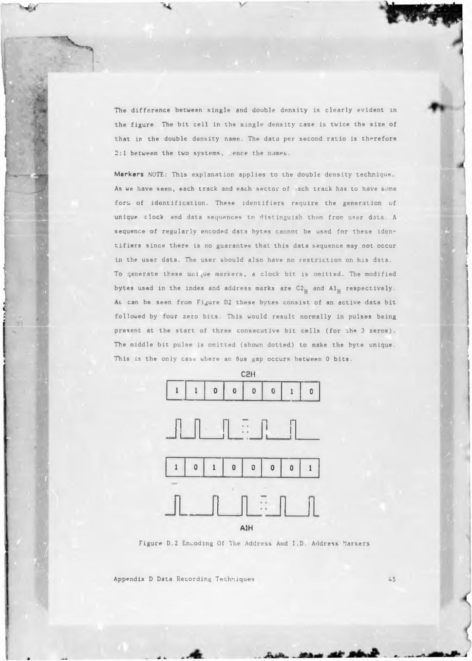
M arkers NOTE: This, explanation applies to the double density technique.
As we have seen, each track and each sector of Mach track has to have some
fora of identification. These identifiers require the generation of
unique clock and data sequences to distinguish them from user d.ita. A
sequence of regularly encoded data bytes cannot be used for these iden
tifiers since there is no guarantee that this data sequence may not occur
in the user data. The user should also have no restriction on his data.
To generate these unique markers, a clock bit is omitted. The modified
bytes used in the index and address marks are C2^ and Al^ respectively.
As can be seen from Figure D2 these bytes consist of an active data bit
followed by four zero bits. This would result normally in pulses being
present at the start of three consecutive bit cells (for the 3 zeros).
The middle bit pulse is omitted (shown dotted) to make the byte unique.
This is the only case where an 8ys gap occurs between 0 bits.
C2H1 1 0 0 0 0 1 0
-,
- —1
-
1 0 1 0 0 0 0 1
A1H
Figure D.2 Encoding Of The Address And I.D. Address Markers
Appendix D Data Recording Techniques 45
W rite Precompensation Peak ahifting i.e. shifting of the position of the
data pulses recorded on the disks is a characteristic of magnetic diuks
that results from interference of adjacent bit flux reversals which cause
a flux reversal to be read slightly befcre or after its nominal time.
Critical bit patterns are Oil, 1000, 110 and 0001. If, for example, we
consider the pattern 11011 the gap between the first two l's is A&mu,s ,
the second two i.e. 101 is Bps and the last two 4ps. The data pulses
corresponding to the l's on either side of the 0 appear to migrate towards
each other thus reducing the Bus gap. By writing the first of these pulses
earlier than normal and the second later than normal, they appear to be
in their correct positions when the- are rend. These early an late writes
are performed by shifting the position of the data pulses 250ns either
way of their nominal positions.
Appendix D Data Recording Techniques 46
APPENDIX £ THE DECODER C IR C U IT R Y
The function of this circuit is to tako the data waveform WD i.e. write
data, which would conventionally be written to the floppy disk, and re
trieve the data and prosont It in a slmiltr form to that which would be
cncounterud on a synchronous communications link, in this case NR2 coding.
It should be recalled that over and above the MFM encoding of the data,
the wave-form has write pre-compensation incorporated as well. The de
coder must also be capable of removing this compensation.
The circuit operates essentially according to the following principles:-
The data waveform is " sampled' to detect the data pulses being writt en
to the floppy disk. These pulse-* are used to reset a counter circuit which
obtains n certain count value in effect measuring the time betwran the
pulses. The counter value is stoiud before the counter is reset. The
counter value that has been stored is than, in effect, quantised thereby
producing an active signal corresponding to one of the three possible
nominal bit spacing* i.e. 4, b or Hus. This together with the previous
data it is used to calculate the present data bit. Clock information is
also generated from the incoming data stream. The NRZ data stream is re
versed on a byte by byte basis (See reason later) after being input to
the 28530 SCC (Synchronous Communications Controller) which performs se
rial to parallel conversion. The remainder of the circuitry is to cater
for special case conditions' which generally cucur at the beginning of
the data stream.
Appendix E The Decoder Circuitry 47
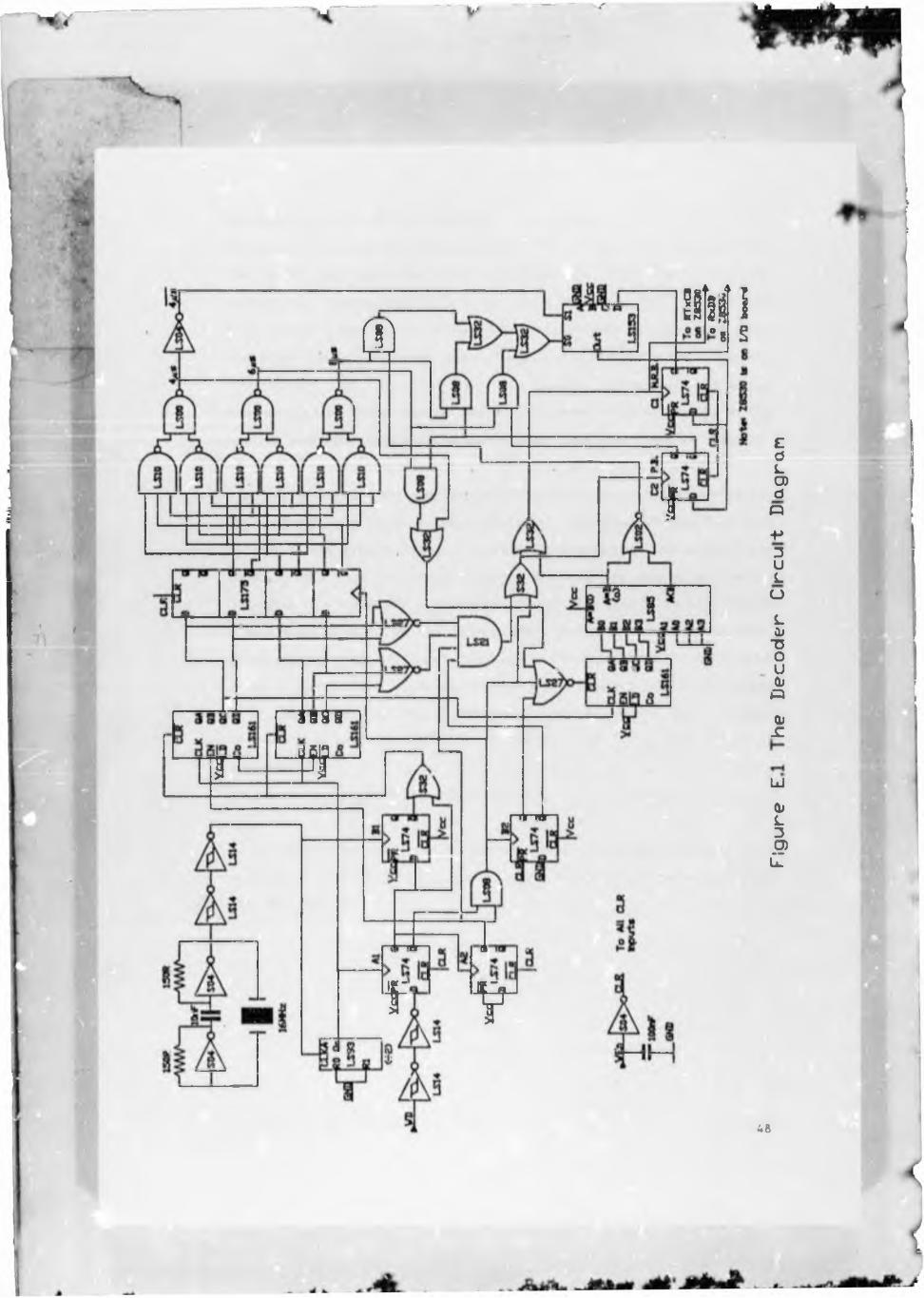
sm:"8 S@
I
$"3512arII rn
1-n
f r
EdLCDdo-K3ULUL0»TJOUfcOcuX
Id<DL3CDiT
ifi

Implementation details St*e Figure El. The inputs lo the circuit are the
WD (Write Data) and WEn (Write Enable). These signals are obtained from
the floppy disk interface after being buffered. A 16 MHz clock is ob
tained from a simple ring oscillator. The Write Enable (WEn) line is used
as a master dear signal to keep the whole decoder circuit in a reset
state when data Is not being input. The pulses occurring on the Write Data
(WD) decoder input are 250ns wide with nominal spacings of 6 or 8ys
between pulses. These spacings may vary by about 250ns either way of the
nominal positions (Write Pre-compensation). The data input is 'sampled'
at hMMz to ensure detection af the pulses In accordance will, the Xyyuist
sampling criterion. The sampling is performed by the D-type flip-flop Al.
Note: The LS74 is positive edge sensitive. The input to this flip-flop
ii preceded by Schmitt-trigger inverters to ensure that the waveform has
an acceptable form before the sampling process. The output of the Al
flip-flop is a 0 when WEn is inactive. The B1 flip-flop is used to provide
a narrow reset pulse on the falling edges of the WD pulses to the LS161
pulse spacing counteis. This occurs in the following manner:- The D input
to B1 is high between pulses which results in a 0 output from the Q* output
of Bl. When a negative edge occurs, the D input is now a 0. The two inputs
to the S32 OR gate an both 0 until the Bl latch is clocked. (Clocking
at 16MHz). When this occurs the latch output is set to a 1 thus termi
nating the reset pulse. See Figure E2.
If the WD line is monitored at the beginning of a write operation, the
waveform shown in Figure E3. The beginning of the write operation occurs
when WEn goes low.
Appendix E The Decoder Circuitry 49
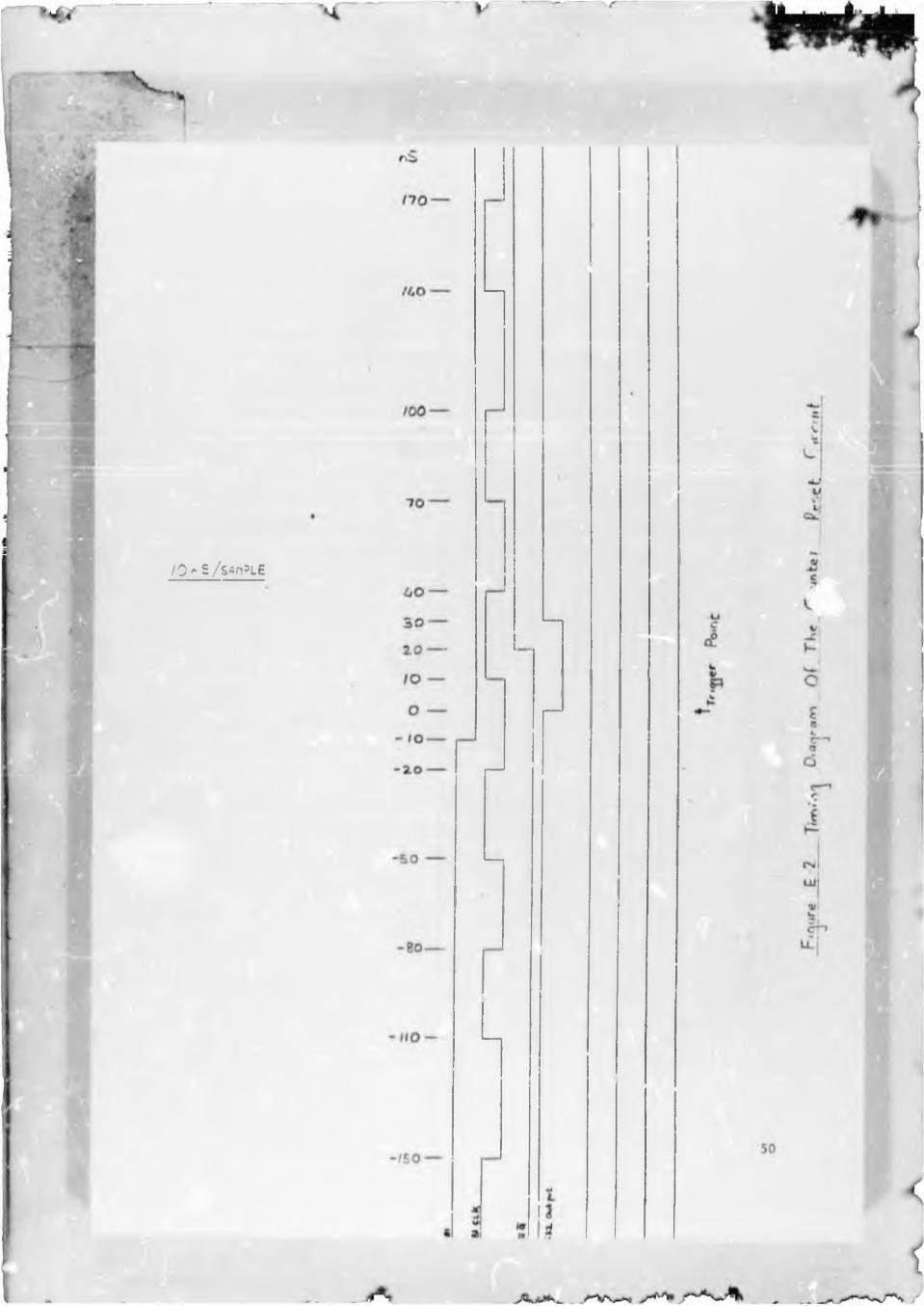
/O * S/SflnPlE
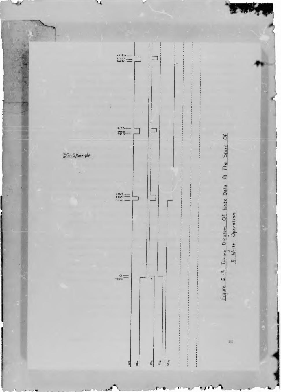
—
--
m s ouq?o./(■SO
g/SO
445 3 43S04(00
As was described above, the LS161 counters are reset on the falling edges
of the sampled WD waveform i.e. The Q output of latch Al. This leads to
an unacceptable situation at the start of the WD pulse train. The counters
begin to count while the sampled WD remains low. The result is that the
first count value latched on the falling edge of the first pulse is too
large. The required period is from the first rising edge ( pt A in Figure
E5 ) to the falling edge of the first pulse. For this reason flip-flop
A2 is included. This is used to disable the counters until a rising edge
is encountered in the waveform. The output then keeps the counters enabled
until the WEn line is deactivated. Flip-flop B2 keeps the third counter
(see function later) in a cleared state and inhibits the pulse expander
circuit (see later) until it is clocked. Latch B2 is clocked whenever a
pulse occurs on WD and latch A2 has enabled the circuit.
The pulse spacing counters are clocked at 6MHz. The outputs of these
counters form the input to two further sections of the circuit viz. the
counter latch LSI75 and the pulse expander (LS27's and LS21). The latter
circuit is used to provide a high output on the LS21 output when all five
counter outputs shown in the circuit diagram are all zero. This only oc
curs when the counter has been cleared (i.e. falling edge of WD). The WD
pulses are only 250ns wide. By combining the counter's outputs whose least
significant bit changes at 1MHz, and ORing this with the 250ns pulses, a
more symmetrical clock is generated for the 28530 SCC.
The data latch is used to store the counter value while the serial data
output is being generated and the next counter value is being generated.
The counter value is latrhed in on the falling edge of WD. i.e. just
before the counters ar ,ct.
As can be seen from Table 1, count values ranging from 24 to 39 make the
4ps output active while values from 40 to 55 and 5o to 71 make the bps
and Bps outputs active respectively. These outputs are obtained by gating
Appendix E The Decoder Circuitry 52
the outputs of the LSI75 latch using the LSOO's and LSlO's. The use of
these signals will be described shortly.
Flip-flops Cl and C2 are used to store the 'Most Recent Bit' (M.R.B.)
produced by the circuit and the 'Previous Bit' (P.B.) respectively.
The 1 previous bit' and the 4, 6 and Bps pulse width signals are used to
control the serial data generator according to the following conditions:-
Note: The 'previous bit' is in brackets. Bold face characters indicate
where data pulses are present.
C O N D IT IO N S DA TA
If 'previous bit' - 1 and Bps is active (1)0l (A)
= 0 and Bps is active (0)00 (B)
(Note: This second case is an exceptional case and only occurs in markers.
See Appendix D on Data Recording Techniques)
If 'previous bit' = 1 and Bps is active (1)00 (C)
= 0 and Bps is active (0)1 (D)
If 'previous bit' = 1 and 4ps is ai.tive (1)1 (E)
= 0 and 4ps is active (0)0 (F)
As can he seen from the above, cases A to C lequire an extra clock pulse
to be generated since there are more data bits than pulses from the WD
1 ine.
Appendix F. The Decoder Circuitry 53
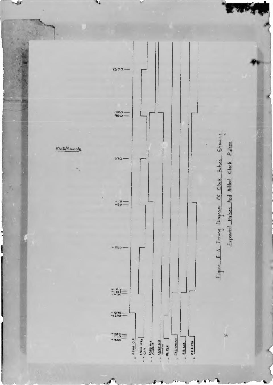
< 0(0icno/oso
On the output of the MFM decoder we require a clock edge for EACH data
bit. To cater for these situations the third LS161 counter is used along
with the LS85 magnitude comparator. This counter is cleared by each pulse
in WD and the counter is kept in the cleared state when cases D to F are
present. These cases are defined by fAim being active) OR (P.B.=0 AND
bps is active). In cas. < to C this LS161 clocks at 1 MHz. During the
second count period, tin A = B output is active due to the wiring on the
A inputs of the LSS5. It is necessary that this output should become
active on such a low count value since all possible bit combinations must
be able to be prccesso i in 4ys i.e. the shortest inter pulse gap. If this
was not the case it may be possible that a new counter value would be
latched before the previous one. had been completely processed.
The 4, 6 and Bps pulse width signals, the A < B output of the LS85 and
the present bit' value are used to drive the select lines of the LS153
(a 1 of 4 multiplexor). This is connected in such a way so as to generate
the required data bit on the output. The flip-flop Cl described above is
clocked cn every clock pulse at the output and thus stores the most recent
data bit. The C2 flip-flop, meanwhile, is clocked only when there is a
data pulse on the WD line. (i.e. stores the present bit).
The derivation of the next data bit in the serial dat^ generator may have
been done using fundamental gating but the use of a multiplexor made the
design easier. The requirements of the circuit are shown below. The fol
lowing should be noted:-
1. The 4, n and bps signals are mutually exclusive.
2. The ’ Present Bit' differs from the ’ Most Recent Bit' only when < i
additional clock pulse is added.
3. (A=B) + (A B) gives a 0 output when the clock pulse is generated and
stays in this state until the counter is reset.
Appendix E The Decoder Circuitry 55
(A=B)+(A<B) P.B.
0 00 11 01 10 00 11 n1 i0 00 11 01 1
4ps 6ys Hys
0 0 10 0 10 0 10 0 10 1 00 1 00 1 00 1 01 0 01 0 0* C 01 0 0
required output.
0100
Doesn't occur 0
Doesn't occur 0
Doesn't occur Doesn't occur M.R.B. (=P.B.) M.R.B. (=P.B.)
The •♦vis line defines a unique requirement and can therefore be connected
directly (after inversion) to one of the multiplexor select lines. The
other select line is controlled by the following equation:-
Sj = SysoP.B.oX + SysoP.B.oX + SysoP.B.oX + biisoP. B . oX + 6ysoP.B.oX
This can be simplified to
Sq = SpsoP.B. + SysoX + 6ysoP.B.
Where X B (A=B) + (A<B) The multiplexor inputs on fhe circuit diagram
correspond to the following select inputs:-
S j S Q i Input
0 0 | D
0 1 | C
1 0 | B
1 1 | A
The data input to thi- Z8530 SCC is obtained from the output of the M.R.B.
latch (Cl). The SCC clock consists of the WD pulses that are expanded as
well as the additional clock pulses from the LS85. Examples ere shown in
Figure F.4. The SCC is synchronised onto the NR7. data stream using
synchronisation characters in the data stream (See Appendix 0 on Emulation
Software;. The SCC converts the serial data into parallel form for the
microprocessor system. In the I/O circuit ry it should be noted that the
data is reversed i.e. the most significant bit is made the least signif
icant etc. since the data written to the disk is written most significant
Appendix E The Decoder Circuitry 56
. - A
bit first and the SCC expects the least significant hit first. This has
-jre serious ramifications for the Encoder circuitry a 111 bi> explained
more fully there.
The MFM decoder performs a vital fv.netion in the emulator by cunvez Ling
the write pre-compensated MFM encoded waveform in;o an NRZ coded waveform
suitable for a SCC. Each building block of the decoder is simple in iso
lation but are combined to perform a complicated task.
Appendix E The Decoder Circuitry 57
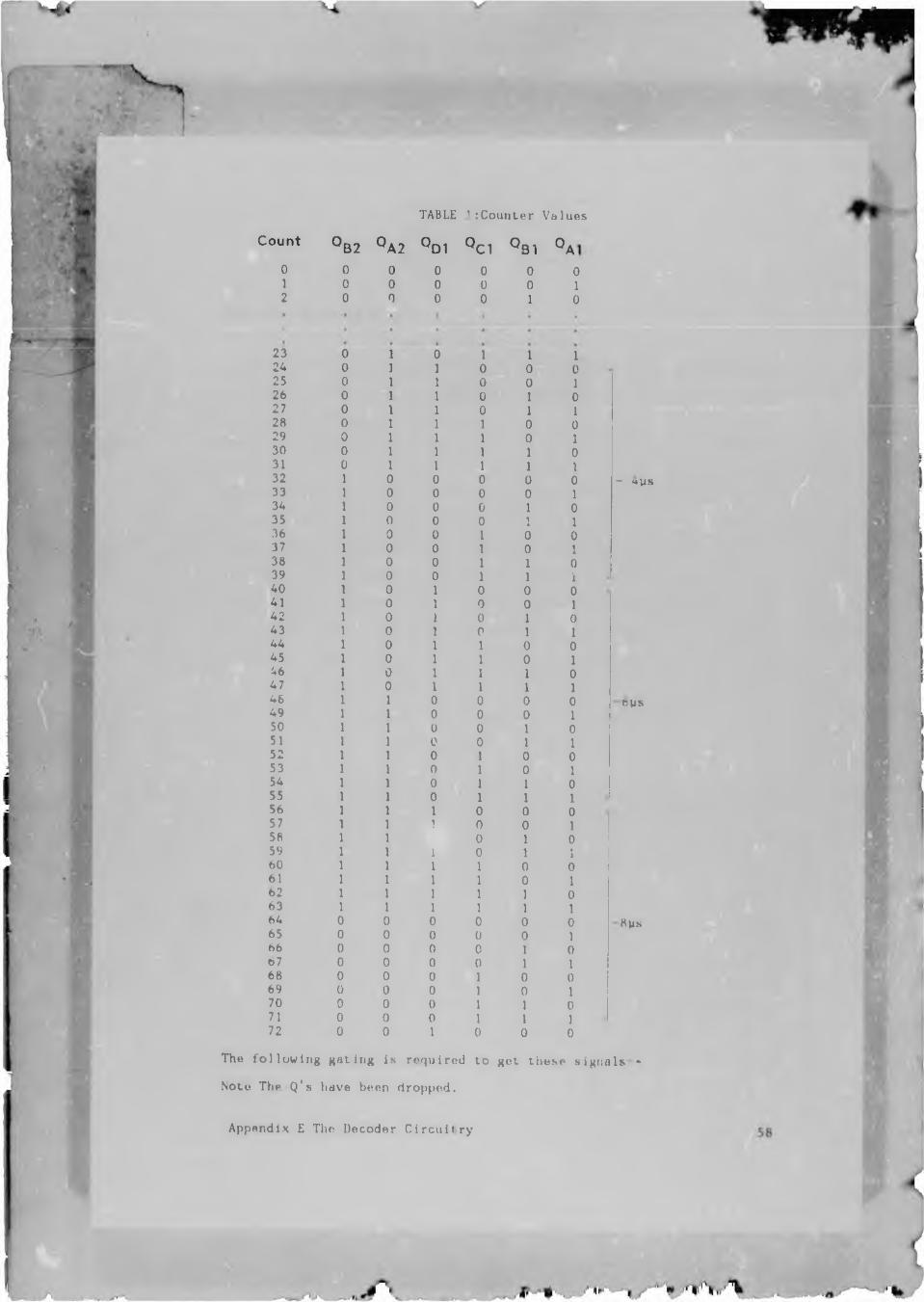
TABLE i:Counter Values
Count °B2 Q A2 °D1 Q C1 Q B1 <o
0 0 0 0 0 0 01 0 0 0 0 0 12 0 0 0 0 1 0
23 0 1 0 1 1 124 0 1 1 0 0 025 0 1 1 0 0 126 0 1 1 0 1 027 0 1 1 0 1 128 0 1 1 1 0 029 0 1 1 1 0 130 0 1 1 1 1 031 0 1 1 1 1 132 1 0 0 0 0 033 1 0 0 0 0 134 1 0 0 0 1 035 1 0 0 0 1 136 1 0 0 1 0 037 1 0 0 1 0 138 1 0 0 1 1 039 1 0 0 1 1 140 1 0 1 0 0 041 1 0 1 0 0 142 1 0 1 0 1 043 1 0 1 0 1 144 1 0 1 1 0 045 1 0 1 1 0 146 1 0 1 1 1 047 1 0 1 1 1 146 1 1 0 0 0 049 1 1 0 0 0 150 1 1 0 0 1 051 1 1 0 0 1 152 1 1 0 1 0 053 1 1 0 1 0 154 1 1 0 1 1 055 1 1 0 1 1 156 1 1 1 0 0 057 1 1 1 0 0 158 1 1 0 1 059 1 1 1 0 1 160 1 1 1 1 0 061 1 1 1 1 0 162 1 1 1 1 1 063 1 1 1 1 1 164 0 0 0 0 0 065 0 0 0 0 0 166 0 0 0 0 1 007 0 0 0 0 1 168 0 0 0 1 0 069 0 0 0 1 0 170 0 0 0 1 1 071 0 0 0 1 1 172 0 0 1 0 0 0
- -*us
oys
Rys
The following gating is required to get these signals -
Note Thr Q's have been dropped.
Appendix E The Decoder Circuitry
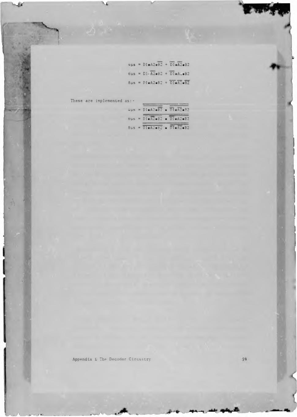
4ms = Dl»A2eB2 + DUA2eB2 bus = D1.A3.B2 + "dT.A-.B2
8ms = D1.A2.B2 + 1)T.A2.B2
T h e s e a r e i m p l e m e n t e d a s :-
A u s = D 1 . A 2 . B 2 * n i . A 2 . B 2
b u s = d 1 . A 2 . B 2 • D l . A 2 . B 2
bus * ni.A2.B2 * rrr./v.B2
Appendix L The Decoder Circuitry
APPENDIX F THE ENCODER C IR C U IT R Y
The encoder circuitry is required to perform the process of providing data
in such a form to the floppy disk interface of the computer so that it
appears to be receiving this data from the disk itself. As the problem
is examined more closely we can see that this requires extensive designing
in both the hardware and software fields since they have a very close
association.
Requirem ents It must be remembered that following the initial formatting
of a disk for use, the floppy disk controller expects to find all the data
recorded during formatting on subsequent disk read operations. For this
reason ALL the data, i.e. including that between sectors needs to be em
ulated. The waveform present on the read data line from the disk-drive
to the floppy disk controller was examined using a logic analyser to as
certain the exact characteristics of the wave-form. If this wave form
could be reproduced as accurately as possible, the floppy disk controller
must surely be convinced that it uas in fact receiving the data from a
disk and thus function as required.
Implementation The wave form consists of an MFM encoded data stream. The
pulso width was measured at 1 ys with nominal pult._ spacing uf 4, 6 and
8 ys when measured from the beginning of one pulse to the beginning of
the next. The voltage levels encountered were typical TTL levels as ex
pected. The data bytes are received MOST significant bit first. On the 5
1/4 inch disk drives as presently found on the IBM PC type computers, the
average bit rata is 250 kbits per second.
A Seriil Communications Controller (SCO is used to provide a number of
fundamental functions viz. parallel to serial conversion and CKC calcu
lation. An important fact must be emphasised at this stage. In a typical
data communication system using this or similar devices, the data is
Appendix F The Encoder lircuitry 60
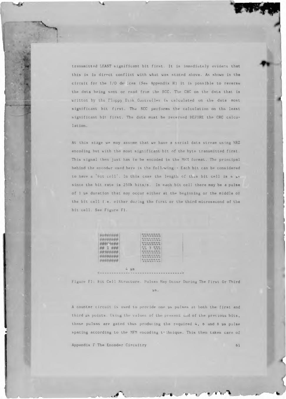
transmitted LEAST significant bit first. It is immediately evident that
this is in direct conflict with what was stated above. As shown in the
circuit for the I/O dc Ices (See Appendix H) it is possible to reverse
the data being sent or read from the SCO. The CKC on the data that is
written by the Floppy Disk Cuntiul lei is calculated on the data most
significant bit first. Thu SCC performs the calculation on the least
significant bit first. The data must be reversed BEFORE the CRC calcu
lation.
At this stage we may assume that we have a serial data stream using NRZ
encoding but with the most significant bit of the byte transmitted first.
This signal then just has to be encoded in the MKM format. The principal
behind the encoder used here is the following:- Each bit can be considered
to have a 1 Bit cell'. In this case the length of this bit cell is 4 wt
since the bit rate is 250k bits/s. In each bit cell there may be a pulse
of 1 us duration that may occur either at the beginning or the middle of
the bit cell i e . either during the first or the third microsecond of the
bit cell. See Figure FI.
4 us
o o o o o o n o o (i o r> •! n o o o n u o o o o o
o n n n o n o *
v. 3 % nOflOOOttOOO O o 1» » u ® S n o n n w o n * o o e o t i o e *
e n e n o o o o • o o v n r o e
Figure FI: Bit Cell Structure. I’ulses May Occur During The First Or Third
U ».
A counter circuit is used to provide one UR pulses at both the first and
third us points. Using the values of the present und of the previous bits,
these pulses are gated thus producing the required 4, 6 and 8 us pulse
spacing according to the MKM encoding technique. This then takes care of
Appendix F The Encoder Circuitry 61
/ I K
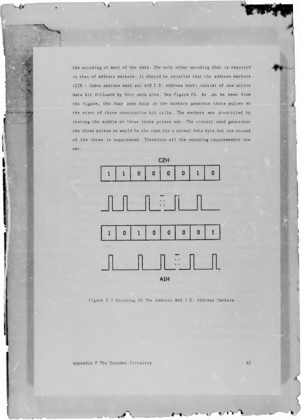
the encoding of most of the data. The only other encoding that is required
is that of address markers. It should be recalled that the address markers
(C2H - Index address mark and AIM I.D. address mark) consist of one active
data bit followed by four zero bits. See Figure F2. As -an be seen from
the figure, the four zero bits in the markers generate three pul:;es at
the start of three consecutive bit cells. The markers are identified by
leaving the middle of three three pulses out. The circuit used generates
the three pulses as would he the case for a normal data byte but the second
of the three is suppressed. Therefore all the encoding requirements are
met.
C2H
1 1 0 0 0 0 1 0
—1 j—1 -n — I—
1 0 1 0 0 0 0 1
A1H
Figure F.2 Encoding Of The Address And I.D Address Markers
Appendix F The Encoder Circuitry 62
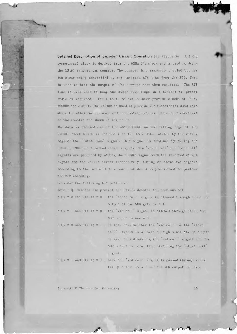
D etailed Description of Encoder C irc u it O peration Sec Figure FA. A 2 MHz
symmetrical clock is derived from the 8MH.C. CPU clock and is used to drive
the LSlbl synchronous counter. The counter is permanently enabled but has
its clear input controlled by the inverted RTS line from the SCC. This
is used to keep the output of the rmmtt»r zero when required. The RTS
line is also used to keep the other flip-flops in a cleared or preset
state as required. The outputs of the counter provide clocks at 1MHz,
500kHz and 250kHz. The 250kHz is used to provide the fundamental data rate
while the other two e used in the encoding process. The output waveforms
of the counter are shown in Figure F3.
The data is clocked out of the 28530 (SCC) on the falling edge of the
250kHz clock which is latched into the LS74 data latches by the rising
edge of the 1 latch load' signal. This signal is obtained by ANDing the
250kHz , 1MHz and inverted 500kHz signals. The 'start cell' and 'mid-cell'
signals are produced by ANDing the 500kHz signal with the inverted 2%0kHz
signal and the 250kHz signal respectively. Gating of these two signals
according to the serial bit stream provides a simple method to perform
the MFM encoding.
Consider the following bit patterns:-
Note:- Qi denotes the present and Q(i-l) denotes the previous bit
a.Qi * 0 and Q(i-l) - 0 , the 'start cell' signal is allowed through since the
output of the NOR gate is a 1.
b.Qi = 1 and Q(i-l) = 0 , the 'mid-cell' signal is allowed through since the
NOR output is now a 0.
c.Qi = 0 and Q(i-l) = 1 , in this case neither the mid-cell' or the 'start
cell' signals is allowed through since the Qi output
is zero thus disabling the 'mid-cell' signal and the
NOR output is zero. thus disabling the 'start cell'
signal.
d.Qi = 1 and Q(i-l) = 1 , here the 'mid-cell' signal is passed through since
the Qi output is a 1 and the NOR output is zero.
Appendix F The Encoder Circuitry 63
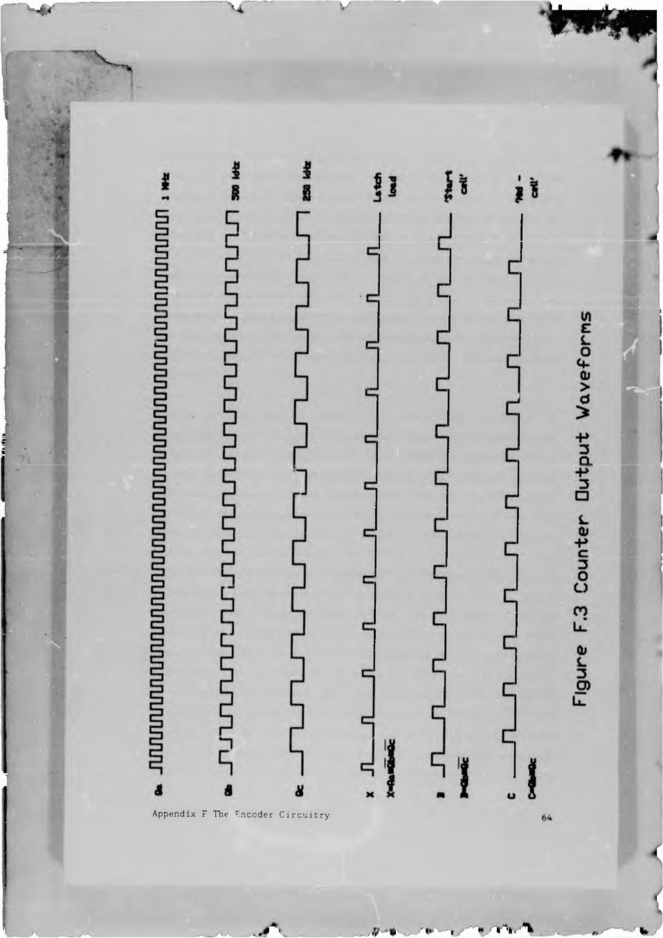
Appendix F The Encoder Circuitry
If wp consider some three bit, bit sequences the operation may become more
clear. If we consider the sequence 101 for example, when Qi is a 1 the
mid-cell' signal is always allowed through as can be seen from cases b
and d above, thus a pulse in the middle of the bit cell is present for
the first 1. in the next bit period then we have Q(i-l) = 1 and Qi “ 0
i.e. case c above. No pulse is allowed at either the start of the bit
cell or in the middle. In the next bit period we have Q(i-l) = 0 and Qi
* 1 i.e. case b above. Here only the mid cell pulse is allowed. If we
consider the spacing between the pulses, we can see that the required 8
Vis spacing is present between the two mid cell pulses. Using a similar
process it can be easily shown that the 6 and 4 ys gaps are produced
correctly.
As was described above the generation of address markers requires that
certain pulses be left out of the encoded stream. As can be seen from
Figure F2 the pulses that are left out to identify the bytes as markers
always occur at the start of the bit cells. An extra piece of circuitry
has been introduced to remove 'start cell' pulses when this is required.
The heart of this circuit is the J-K flip-flop. The output of this flip-
flop is ANDed with the 'start cell' signal i.e. the signal is suppressed
if the flip-flop output is a 0. The flip-flop is held in a preset state
i.e. Q=l when the encoder is disabled (via the DTK line and AND gate) and
it is also preset whenever a midcell pulse is produced (i.e. a 1 bit is
encoded). This is done to ensure that the flip-flop always allows the
required 'start cell' bits to pass through until it is necessary to remove
these pulses. The J and K inputs to the flip-flop are both tied high and
thus the output toggles on each applied clock. (Negative edge sensitive).
What happens then (assuming th*> ’ start cell' stream to be clocking the
flip-flop i.e. the. AND gate on the clock input by-passed) is that the
output, initially 1 and thus allowing passage of the signal, changes state
to 0 and thus prevents the next pulse from reaching the output. The
falling edge of this pulse does, however, restore the flip-flop output
Appendix F The Encoder Circuitry 65
to the 1 state. It is immediately evident therefore that this flip-flop
must only be allowed to operate during address marker generation. This
is done via the remaining O-type flip-flop whose output is held at 0 by
the DTK line of the Z85'30 that controls the clear input of the flip-flop.
The output is only allowed to attain the 1 state when it is clocked by a
1 in the data stream from the Z3530. This is advantageous since the DTR
line can be set as soon as the address mark data is written to the Z8530
without having to worry about the delays encountered in the encoder cir
cuit. A necessary condition for this to work is that there, are no 1 hits
in the data stream between the DTR line being asserted and the address
mark data arriving at the data latches. This condition is satisfied since
the address markers are always preceded by 12 00H bytes. Sv.s Appendix A.
The J-K flip-flop needs to be reset for each address mark byte since the
output would toggle to 0 on the first pulse, toggle to 1 on the second
and back to 0 on the third. It must, however be in the 1 state at the
start of the next address mark byte. Care must be taken when writing the
software that controls the DTR line since this line must remain active
until all three address markers have passed through the encoder. The
inclusion of the flip-flop chain on the ,1-K preset line ensures that only
three address markers can be generated. Th<> DTR line can be left in the
active state longer thus making the software less critical. After the
three markers have been generated the tlip-flop is forced into the preset
state.
The waveform available from the MFM encoder is buffered before being ap
plied to the floppy disk interface. The waveform produced by the circuitry
is identical to that obtained from a floppy disk drive unit. All that
is required is the software to provide the data expected by the Floppy
Disk Controller and to control the SCC control lines. This is described
in Appendix P.
Appendix F The Encoder Circuitry 66
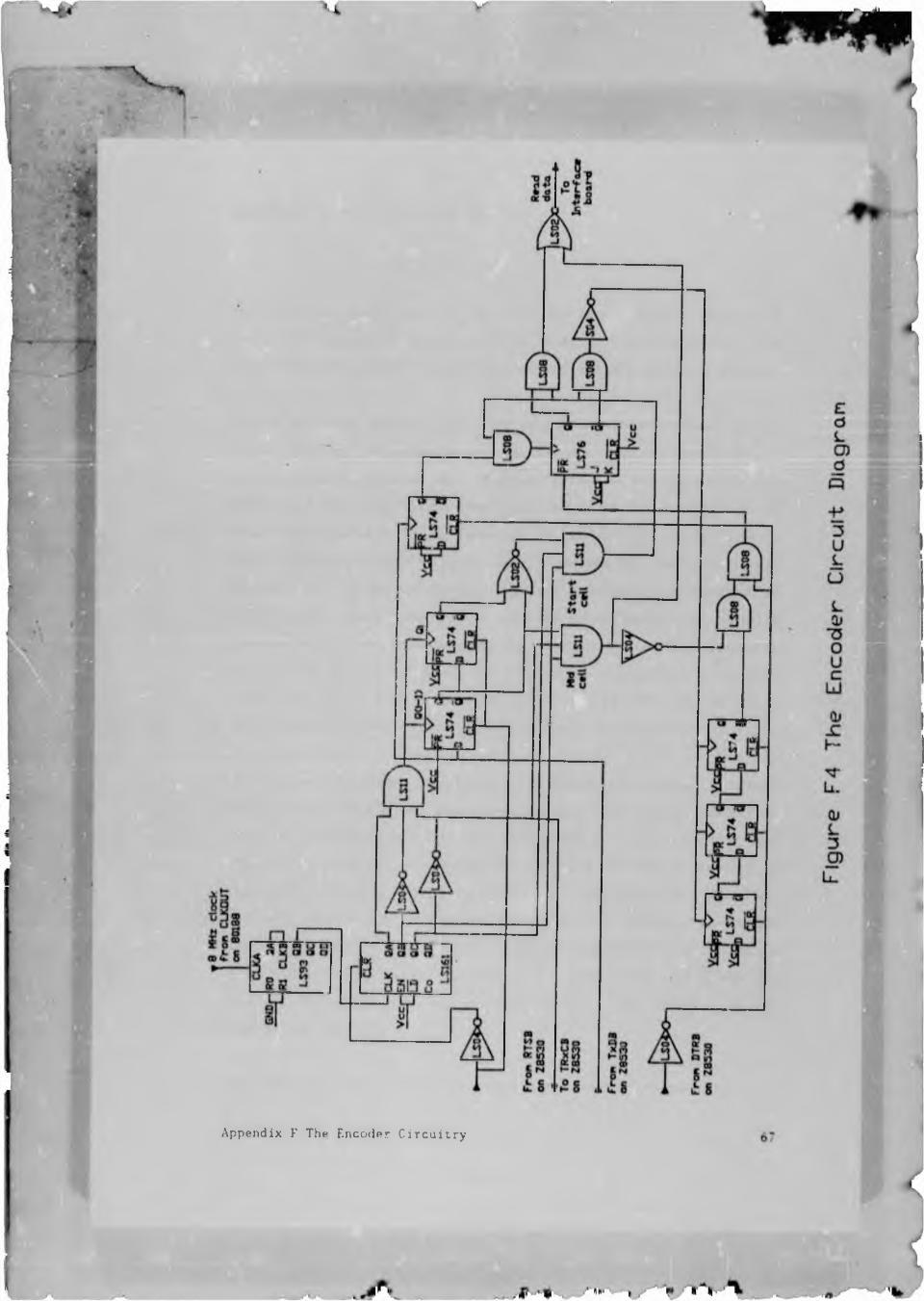
"
Appendix K The Encoder Circuitry
APPENDIX 0 THE INTERFACE BOARD
The interface board contains the input and output buffers required to
interface the emulator circuitry to the floppy disk interface cable. The
track counter to monitor the head movement is included in this circuitry.
Most of the lines on the interface cable are ’bus' signals except for the
select lines for the individual drives. All the lines are however driven
by open collector drivers. All the inputs therefore require pull-up re
sistors and 150Q resistors are used since this is the value used on normal
disk drive units. All the inputs except the select input are buffered by
D-type latches. In this way the state of the bus is retained when the
emulator is no longer selected. The select line itself is inverted to
enable these latches as well as to cause the output NAND drivers to drive
th*» bus. Most of the signals sources and destinations are self explanatory
but some are worthy of mention. The Index pulse is generated by software
which controls the I'TR line of channel A of the Z8530 SCC. The VP signal
is permanently disabled by grounding the input. See Figure Gl.
The head motion is monitored by an 8 bit up/down counter that is driven
by the DIR and STr.P lines. Step pulses are generated for each track that
is to be traversed. The DIR line determines in which direction the
counting takes place i.e. towards the centre or outside of the disk. A
low on DIR causes the count value to increase (equivalent to inward head
movement). The counter outputs are OKed together to generate the TRACKO
signal which, as its name implies, is active when the counter's value is
zero. A simple port allows the counters' outputs to be read by the CPU
when the PCS3 and RI) lines are low simultaneously. Note:-PCS3 is an I/O
chip select line from the 80188 CPU.
This board provides a simple yet critical function in the emulator.
Appendix G The Interface Board 68
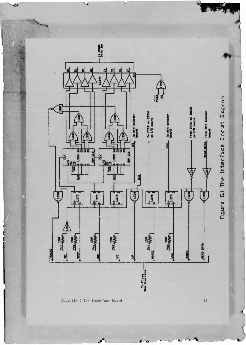
IOrnw— 1
. .
A
is
Appendix G The Interface hoard 69
Figu
re
G.l
The
Inte
rfa
ce
C
ircu
it D
iagr
am
APPENDIX H THE MICROPROCESSOR CONTROLLER UNIT
See Figure HI.
The microprocessor unit's functions ore to control the network and floppy
disk drive emulation. The 80188 microprocessor forms the core of the unit
and is supported by 2 Z8530 SCC's, a parallel input port (tri-state
buffer), a parallel port (latch'' as well as 2S6K of RAM which is expand
able to just under 1 Mbyte in 25bKbyte increments. 8Kbyte? of EPROM is
also allowed for.
The microprocessor controller unit consists of 3 boards viz. CPU, memory
and I/O boards and each will be discussed individually an far as possible.
It should be noted however that eventhough the tern boards has been used
this refers to logical divisions rather than physically separate circuit
boards.
The CPU board See Figure H2.
The only requirements for the internal oscillator of the 80188 micro
processor is a IhMHz crystal and 2 20pF capacitors as specified by vhe
manufacturer. Tho IhMHz crystal provides an 8MHz processor clock and an
8 MHz 50*. duty cycle clock on the CLKOUT line. The RES input is connected
to a conventional RC reset circuit. The component values are R=1K0 and
C*22vF which keep RES low long enough after power-up to satisfy the reset
input requirements. The low to high transition on RES must occur no sooner
than 50us after power-up|4]. The RESET output indicates that the 80188
is being reset internally, is synchronised with the system clock and can
be used as a master reset. In this cast it is only used to reset the Z8530
SCC. The unused inputs viz. HOLD, SRDY, ARDY, TEST, INTI, NM1 , IT2 and
IT3 are tied to Vcc or GNU depending on their respective inactive states.
Appendix H The Microprocessor Controller Unit 70
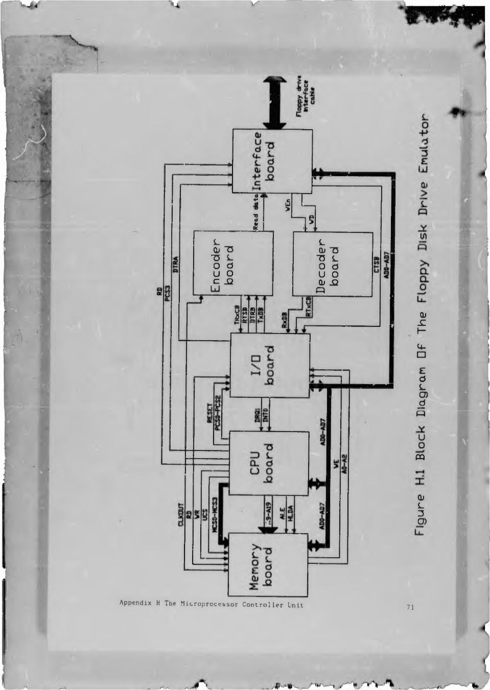
u
■ dJk■Hs
■o
1 15
» <
L L(Li 73 m 13
T5 L 73 Lo d o du o u oC _Q Oj _Q
U «
m CDs:h-
Q_□£dLO)d«
Uo
PQ
(DL3O)
Appendix H The Microprocessor Controller Lnit 71
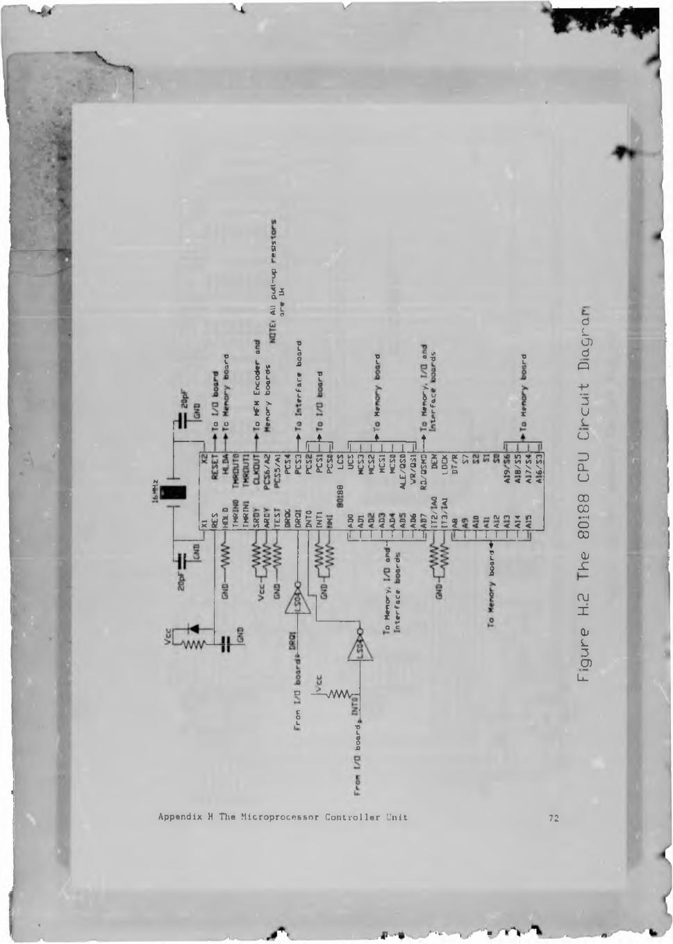
V
' #
'A
.
S p
rd
o o
Ni|\0 I
I1t
&
S tU
d
IIU S3 X >
n
■oIs£du.I
uL
TE -■8
£ ifl - d l -..T Z i L j . i x l
"OE
i
!|g8ggp§o^S
1115g “ G_l o O'«
sSiilxiSiSil* 11555511^?5 5
TT~ri"TTTTo — ru n
< < <
T
d "D L
if0 cD -^- V W W -
§L •eL1a
T T T T T
m n 10 n nX X \00 X <JJ < < <
5STeLI
dL(J)dO
•P*5uLU
Z)CLu00CO*""4o00
cuJZ
OJX
OjL3O)Ll_
Appendix H Tlie Microprocessor Controller Unit
JP ’• 'IV , , w
72
X L I d
20pF
From I/O b o a r d s
I/O b o a r d s
"]uND
16MHz
G h D ~ —
GND —
i-AAAAA-L- W v \ ^
To Memory, I/O and - In te r fa c e b o a rd *
r A M A A - ^ - A W / —
To Memory b o a rd *
T eopF
XI X2 —RLS RESET — ► To I/O b oardHOLD HI DA — ►To Memory boardTMHINO TMKOUTOTMRINl TMROUT1SRDY r.LKOUT — ►To MFM Encoder andARDY PCS6/A2 Memory b oardsTl ST PCSS/A1DKQO PCS4DRQ1 PCS3 ► To In te r fa c e b oardINTO PCS2 =1INTI PCS1 “ -»To I/O b oardNMI peso
80188 LCSADO u c sA 01 MCS3 —AD2 MCS2AD3 MCSl — To Memory b oard
ADA MCS0 —ADS ALE/QSO —A 06 VR/OS1 ■=.
AD7 RD/OSMD — ►To Memory, I /O andIT 2 /IA 0 D E N In te r fa c e b oards1T3/IA1 LOCKA8 DT/RA9 S7A10 S2Alt SIA12 SOA13 A19/S6AM A18/S5AI5 A17/S4
► To Memory b oard
Alt, 1
a re Ik
F ig u r e H,2 The 80188 CPU C i r c u i t D iagram
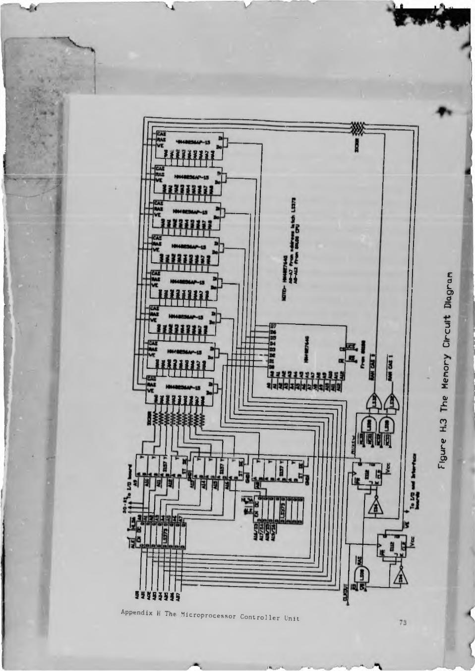
XL
i m m h
i
it
m m -
B m fcm r n i
IB! 1
99SS353S
EdLO)d«
3 U LU
LOcQ#X0/X
n xOf53>U-
Appendix H The Microprocessor Control 1er Unit
The Memory Board See Figure H3.
Note the sources of the address lines on the HN4827b4G EI’ROM.
The first requirement for both memory and I/O devices is for the lower
address lines AO - A7 and upper lines A16 - A19 to be de-mu 11iplexed. On
the 80188, the former group is multiplexed with the data lines while the
latter group is multiplexed with some status lines. This is done simply
using two LS373 latches which are enabled by the ALE (Address Latch Ena
ble) line of the 80188. The outputs of the memory mapping unit in the
60188 are programmable thus allowing these lines to be activated at var
ious positions in memory. The memory map of the microprocessor unit is
shown in Figure H4. Address lines A0-A2 are provided in their de
multiplexed form for use on the I/O board. The EPROM is located at the
top of memory since the reset vector is located at FFFFOH. The position
of the DCS (Upper Chip Select) line is progiammed to become active at
FE000H. EPROMS with access times of up to 250ns can be used with a CPU
clock frequency of 8MHz.
It is possible to use four banks of 256K RAM chips to give (1Mbyte-EPROM
size)K bytes of RAM. If more than 512K is used, chip select lines have
to be generated due to a peculiarity of the 80188. The four MSC (Mid -
range Memory Chip Select ) lines are used to enable the lower 512K i.e.O
to 512K. The chip select lines for the area above this would have to be
generated using UCS and A19 and A18. LCS (Lower Memory Chip Select) is
not used in this design. MCS0 and M0S1 select 0 to 256K while MCS2 and
MCS3 select 256 to 512K.
The 256K RAM chips have 9 multiplexed row/column address lines. Address
lines A0 to A 17 are multiplexed to provide the required 4 lines i.e. MAO
of the RAM is switched between AO and A‘> of tne processor. The RD and WR
lines of the processor are used to generate the RAS signal for the RAM.
The RAS line also controls the operation of one of the S112 J-K flip-
flops. When RAS is active and the flip-flop is clocked by the CLK0UT line
of the 80188, the output changes thus switching the address multiplexor.
Appendix H The Microprocessor Controller Unit 74
The multiplexor should therefore switch at the start of the T3 CPU cycle.
See Figure H5. The actual CAS signals applied to the RAM chips is a
combination of this multiplexor switching line and the Chip Select lines.
Resistors are included on the inputs to the RAM chips in an attempt to
keep the voltage overshoots and ringing that can occur to a minimum.
The WE enable inputs of the RAM chips as well as that of the Z8530 require
that the data to be written be stable on the data bus before this line
is active The WR line of the 80188 does not satisfy this condition and
a WE signal is generated by allowing the output of the SI 12 J-K flip-flop
controlled by WR only to become active on the rising edge of CLKOUT fol
lowing the activation of the WR line. Again this should correspond to
the start of the T3 CPU cycle.
The RAM chips require each row to be refreshed every 4ms Considering that
there are 256 rows that require refreshing, and assuming refreshing is
done on a regular continuous basis, a refresh cycle is required every
15.625us. The refreshing is done by programming one of the timers in the
80188 to request a memory DMA cycle. See Appendix 0. Each of these cycles
refreshes an entire row of the memory.
Appendix H The Microprocessor Controller Unit 75
ucs
MCS3
MCS2
MCS1
MCSO
FFFFFH
FEOOOH
COOOOH
80000H
40000H
OOOOOH
8K EPROM
256K DRAM
768K
512K
256K
Figure H.4 The Memory Map OF The 80188
Appendix H The Microprocessor Controller Unit 76
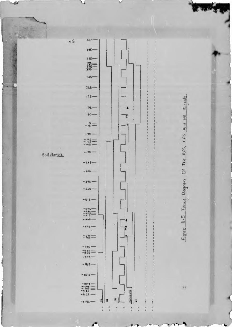
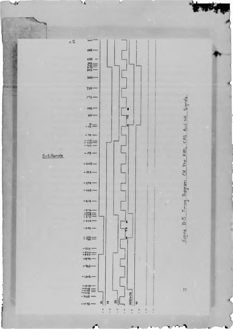
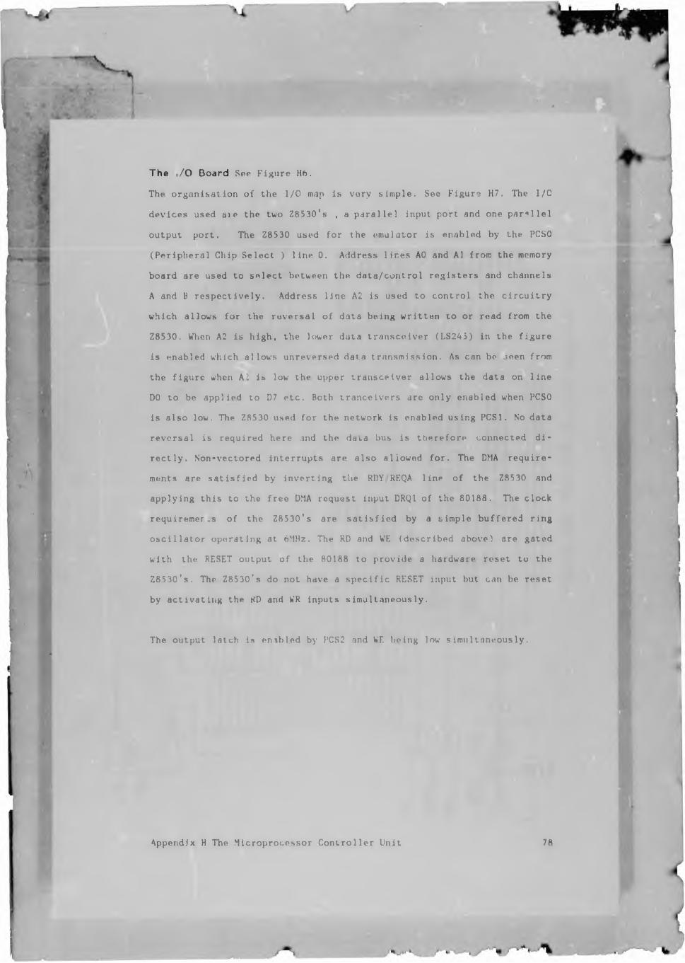
The i/O Board See Figure H6.
The organisation of the I/O map is very simple. See Figure H7. The I/C
devices used aie the two Z8530's , a parallel input port and one parallel
output port. The Z8530 used for the emulator is enabled by the PCSO
(Peripheral Chip Select ) line 0. Address lines AO and A] from the memory
board are used to select between the data/control registers and channels
A and B respectively. Address line A2 is used to control the circuitry
which allows for the reversal of data being written to or read from the
Z8530. When A2 is high, the lower data transceiver (LS245) in the figure
is enabled which allows unreversed data transmission. As can be joen from
the figure when A2 is low the upper transceiver allows the data on line
DO to be applied to D7 etc. Both tranceivers are only enabled when PCSO
is also low. The Z8530 used for the network is enabled using PCS1. No data
reversal is required here and the data bus is therefore connected di
rectly. Non-vectored interrupts are also allowed for. The DMA require
ments are satisfied by inverting the RDY RF.QA line of the Z8530 and
applying this to the free DMA request input DRQ1 of the 80188. The clock
requiremer.s of the Z8530's are satisfied by a simple buffered ring
oscillator operating at 6MHz. The RD and WE (described above) are gated
with the RESET output of the 80188 to provide a hardware reset to the
Z8530's. The Z8530*s do not have a specific RESET input but can be reset
by activating the RD and WR inputs simultaneously.
The output latch is enabled by PCS2 and WE being low simultaneously.
Appendix H The Microprocessor Controller Unit 78
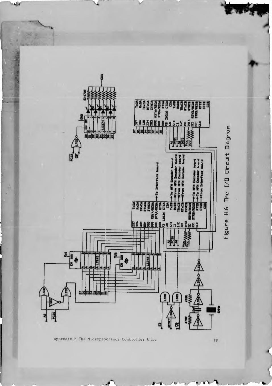
IE 1SgiSigglssSBSsiBaay s a s s a - H g
m in
si Ii i i i igg iB tStiS iiSBBa
B - g
Appendix H The Microprocessor Controller Unit
Figu
re
H.6
The
I/O
Circ
uit
Dia
gram
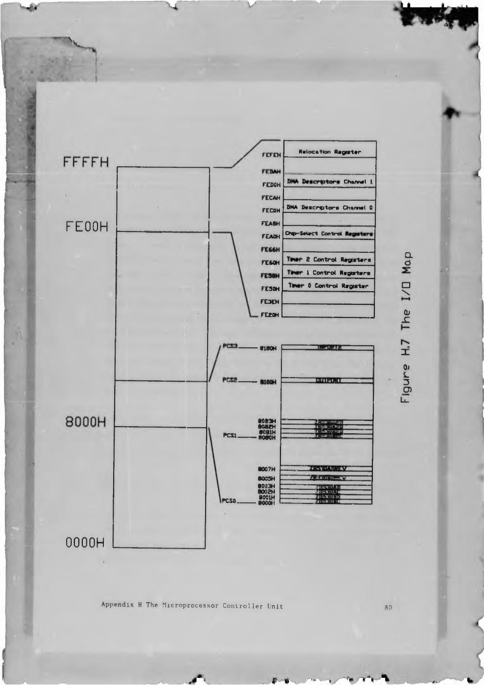
Relocation R»gttrterFETCH
Channel 1FEDOH
FECAHDMA D escrip to rs Channel 0FECOH
FEOOH FEA8HCh<>-$etect ControlFEAOH
2 Control RegistersFEMH1 Control Registers0 Control RegisterFE30H
FE3EH
FL20H
eieoH
8083HeoatHeoeiH8080HPCSl
8007H 8003H B003H 800PH 8001H 8000HPCSO
OOOOH
CL d
□\
(U JC
%
0)L3O)L_
Appendix H The Microprocessor Controller Unit RO
/ Iflw
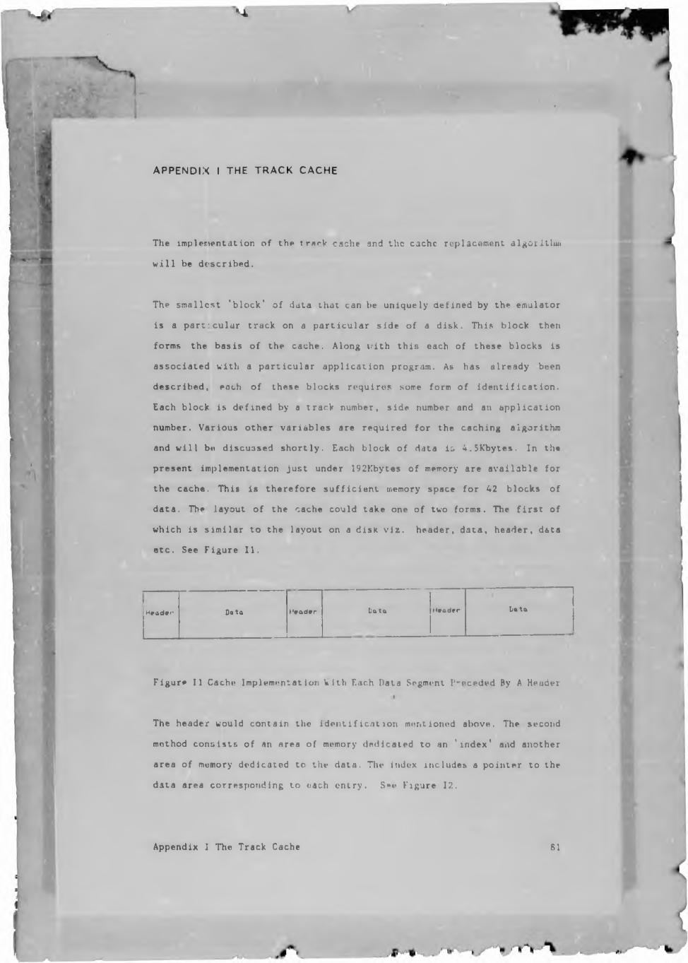
'A
A P P E N D IX I THE T R A C K CACHE
The implementation of the tr«rV. cache and the cache replacement algorithm
will be described.
The smallest 'block' of data that can be uniquely defined by the emulator
is a particular track on a particular side of a disk. This block then
forms the basis of the cache. Along with this each of these blocks is
associated with a particular application program. As has already been
described, each of these blocks requires some form of identification.
Each block is defined by a track number, side number and an application
number. Various other variables are required for the caching algorithm
and will be discussed shortly. Each block of data ia 4.SKbytes. In the
present implementation just under 192Kbytes of memory are available for
the cache. This is therefore sufficient memory space for 42 blocks of
data. The layout of the cache could take one of two forms. The first of
which is similar to the layout on a disk viz. header, data, header, data
etc. See Figure II.
Header* Data Header Lata Header lota
Figure II Cache Implementation V1th Each Data Segment Preceded By A Header
The header would contain the identification mentioned above. The second
method consists of an area of memory dedicated to an 'index1 and another
area of memory dedicated to the data. The index includes a pointer to the
data area corresponding to each entry. S«e Figure 12.
Appendix I The Track Cache 81
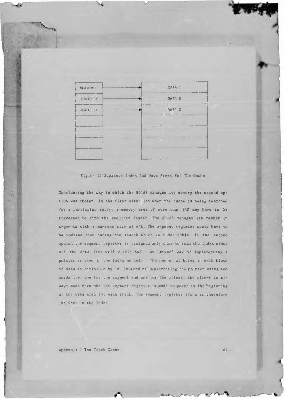
---------- --------HEADER I DATA 1
HEADER 2 □ATA 2
.... - .... - ..... ^HEADER 3 ’)Af A 3
•
Figure 12 Separate Index And Data Areas For The Cache
Considering the way in which the 80188 manages its memory the second op
tion was chosen. In the first situ/ ion when the cache is being searched
for a particular entry, a memory area of more than 64K may have to be
traversed to find the required header. The 8(188 manages its memory in
segments with a maximum size of o4K. The segment register would have to
he updated then during the search which is undesirable. In the second
option the segment register is assigned only once to scan the index since
all the data lies well within 64K. An unusual way of implementing a
pointer is used in the index is well. The number of bytes in each block
of data is divisible by 16. Instead of implementing the pointer using two
words i.e. one for the segment and one for the offset, the offset is al
ways made zero and the segment register is made to point to the beginning
of the data area for each track. The segment register a 1 one is therefore
includes in the index.
Appendix I The Track Cache 82
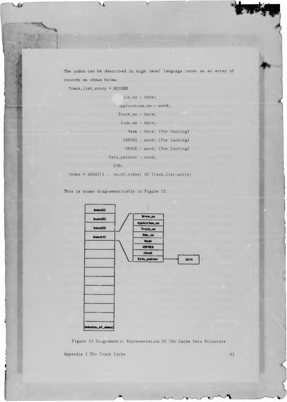
The index can be described in high level language terms as an array of
records as shown below.
Track_list.entry = RECORD
ive_no : byte;
.%ppl ication_no : word;
Track,no : byte;
Side_no : byte;
Mask : byte; (For Caching)
XBFREQ : word; {For Caching)
XBAGE : word; {For Caching)
Data_pointer : word;
END;
Index ■ ARRAYj1 •• no_of_sides] OF Track_list_entry;
This is shown diagrammatically in Figure 13.
XBAGC
DATA
Figure 13 Diagrammatic Representation Of The Cache Data Structure
Appendix I Thi* Track Cache
I I
!
83
Managing the cache is a simple task until all the blocks in the cache are
filled. The problem then arises as to which block should be overwritten.
Decision algorithms in common use are random replacement, First In / First
Out (FIFO) and Least Recently Used (LRU). In large caches the performance
of those algorithms is much the Bam»[5 j .The key to the benei technique
proposed by McKeon [6] is to measure the frequency of access of a block
and use this in combination with when last the block was used when making
the replacement decision. The additional information in the RECORD above
is to implement tnis algorithm. The Mask is to indicate whether a block
is in use and whether a track has been updated i.e. written to, but has
not yet been updated on the file server. XBFRF.Q is used for the frequency
of access while XBASE is for when last the block was used.
When a block is found in the cache (a 'hit'), the frequency of access
parameter (X3FREQ) is increased. When a block is not in the cache (a
miss') and no nutters are free, the cache is scanned to find a block with
the lowest, frequency of use i.e. lowest XBFRF.Q and tnis block is replaced.
If multiple blocks with the same lowest frequency of use are found, then
the block that has not been used for the largest amount of time is re
placed . This decision is made using the XBAGE parameter. It is obvious
that copies that stay in the cache have a better chance of being found
and therefore the XBFREQ parameters will continue to increase. This pa
rameter is 'decayed* over a period of time otherwise some blocks would
remain permanently in the cache. The decay process is implemented by
halving the XBFREQ parameter every sixteenth call to the cache. The reason
for halving every sixteenth call is that these functions can be performed
conveniently and quickly using masking and rotates. The XBFREQ parameter
is increased by 128 for each 'hit . Using these values, even in the worst
case where the same blo~k is accessed repeatedly, the XBFREQ parameter
cannot overflow. The maximum that XBFREQ can attain is lt> X 128 + i X 16
X 128 + i X 16 X 28 + ... which can be recognised as a geometric
Appendix I The Track Cache 84
progression. In the limit then the maximum value that can be reached is
2 X 16 X 128.
A high level description of the replacement algorithm, based on the data
structure described above, is shown below.
CONST
no_of_sides ■ 42; (Maximum number of tracks in cache }
in.use = 100000008; (Bit mask indicating block in use }
VAR
devioage : word; (Global variable)
BEGIN
devioage := 0; (Initialisa variable in main program)
PROCEDURE get.block (reqdrive, roq eqtrack : byte,
reqAppln.no : word,
VAR data.point : word);
V A R
index.posn : byte;
BEGIN
devioage := devioage + 1; {increment global age for each routine access
IF devioage = 16 THEN
FOR index posn := 1 TO no_of.sides DO
WITH index}i) DO
IF ((Mask AND in.use) = 1) THEN
XLFREQ := XBFREQ DIV 2;
(If block in use then halve the frequency of access }
Findblock(reqdrive, reqside, reqtrack, reqAppln no, status, index posn);
IF status = successful T H E N
WITH index[index.posn] DO
BEGIN
XBFREQ := XBFREQ +128; (Record a hit)
XBAGE :* devioage; (Update access age)
data point := data pointer (Set pointer to data area)
Appendix I The Track Cache 85
status := successful;
END
ELSE BEGIN {block not in cache)
allocate_block (index_posn);
WITH indcx(Index posn] DO
BEGIN
Drive := reqdrive;
Side := reqside;
Track := reqtrack;
Application_no := reqAppln no;
Mask in.use;
XBAGE := devioage;
XBKREQ := 0;
data_point := data_pointer;
END;
get _ data (data pointer);
END;
PROCEDURE Findblock (reqdrive, reqside, reqtrack : byte;
reqAppln no : word;
VAR status index posn : byte);
BEGIN
index posn := 0;
REPEAT
index .posn := index posn + I;
UNTIL (index[index posn].Drive = reqdrive AND
indexjindex posn].Side = reqside AND
index]index posn].Track = reqtrack AND
index] index poan] .Application no - reqAppln.. no)
(index posn = no of sides);
status := NOT (index posn = no of sides);
END;
Appendix I The Track Cache
PROCEDURE allocate_block (VAR index, posn : byte);
VAR
age, freq, oldest : word;
i, marker : byte;
BEGIN
index.posn := 0;
REPEAT
index.posn := index posn 41;
UNTIL ((index}index posn].Mask AND in.use) = 0) OR
(index_posn * no of.sides);
status := NOT (index.posn = no of sides);
IF NOT status THEN
BEGIN
freq := 32767; (Find XBFREQ smaller than this)
oldest :* 0;
FOR i:= 1 TO no.of.sides DO
WITH index[i] DO
IF ((Mask AND in use) =1 ) AND ((Mask AND write)
THEN IF XBFREQ <= freq THEN
BEGIN
freq := XBFREQ;
age := devioagc - XBAGE;
IF (age > oldest) THEN
BEGIN
oldest := age;
marker := i;
END;
END
END
END;
Appendix I The Track Cache

Tho get_blook procedure would be called each time data is required from
the cache. The procedures are then called as required. The get data pro
cedure is not described here but this procedure's responsibility is to
obtain the required data from the file-server and insert it at the area
starting where data pointer is pointing to.
Appendix 1 The Track Cache 88
APPENDIX J WHY 'STAR-BUS' NOT ETHERNET
The disk drive emulator board has a nett data rate of 250Kbits per second
between it and the P.C.. To provide each user with a response time com
parable to that of a floppy disk, the network must be capable of providing
data at a sufficient rate. To illustrate the needs of the network a
loading situation that was described earlier to be possible in this type
of environment will be considered viz. a number of users simultaneously
request ing data that has to be fetched from the file-server. The emulation
of a track of data takes approximately 200ms. If we take a number of em
ulators each successively requesting data from the file-server we can
obtain a feel for the bit rate necessary for the network. A bit rate of
250Kbits per second would therefore sustain the needs of one emulator.
If we take a system with 25 P.C.'s the required bit rate can * calcu
lated.
D a to rate =■ S O AC bits x 2 G
~ ' S’* 11 ti p i f t f o'-) cl
An Ethernet type system with a bit rate of 10 Mbits per second would
therefore satisfy the requirements from the bit rate point of view, This
has some significant cost implications as will be discussed shortly.
Looking at a simpler twisted pair type network with transmission speeds
of the order of 1 Mbit per second we find that the operation of a maximum
of four 'simulators can be sustained. This therefore does not provide very
extensive networking capabilities. Typical maximum transmission speeds
that can be achieved with common communications controllers is 1.25Mbits
per second. This increases the maximum number of emulators to five. The
possibility of constructing a star type network with the file-server at
the hub was considered. Each ray of the star would consist of a bus
structure operating at 1.25Mbit per second. The number of these rays could
Appendix J Why 1Star-bus1 not E.hernet 89

be increased until sufficient nodes could be catered for. In this way an
equivalent effective throughput of the Ethernet system could be achieved.
As always these two systems have compromises. In the first instance the
cost and complexity per emulator would be increased considerably since
hardware capable of providing these high bit rates has to be provided.
The file-server would only require one of these Ethernet type controllers
and would therefore be less complex than that for the star system. For
the second system each emulator need only be capable of transferring data
at 1.25Mbits per second that can be handled by a communications control
ler. The emulator's network complexity is therefore limited. The file-
server is however far more complex than in the first case. A
communications controller is required for each of the rays of the star.
The bus access is less contentious however having fewer nodes on each bus
since there are a number of busses running in parallel.
The added complexity of the file-server is worthwhile when the costs for
the Ethernet type system are considered. Although the system may be com
plex, the individual components on the file-server board are relatively
cheap. The overall system is therefore substantially cheaper. The
Ethernet type interface would make the goal of the P.C. interface price
being comparable to that of a disk drive, impossible to attain. Typical
prices for Ethernet controllers alone are of thj order of R200 while the
communications controllers in question are of the order of K20. The wiring
and installation costs are also substantially cheaper than those associ
ated with a coaxial cable based system.
Appendix J Why 'Star-bus' not Ethernet 90
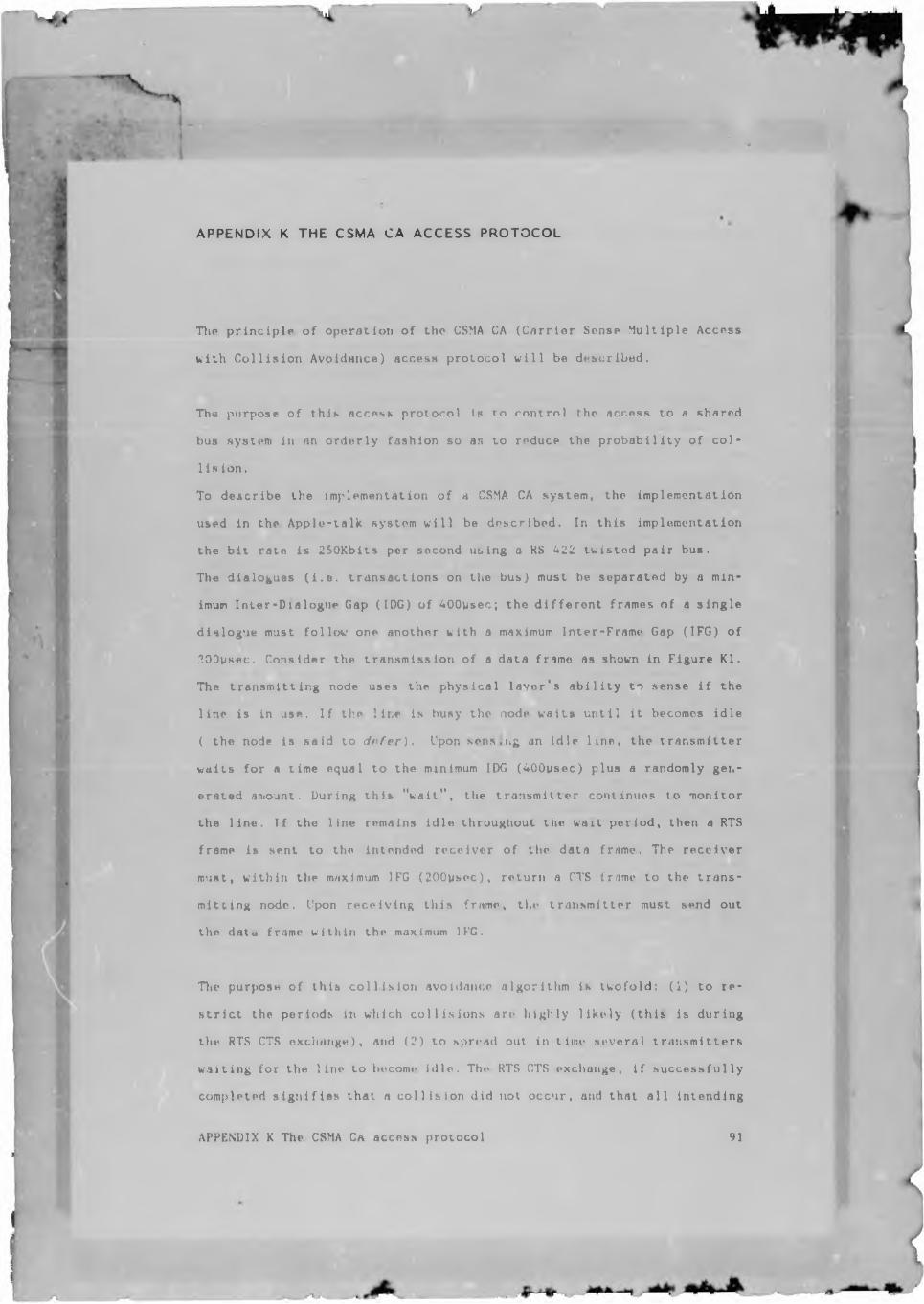
APPENDIX K THE CSMA CA ACCESS PROTOCOL
The principle of operation of the CSMA CA (Carrier Sense Multiple Access
with Collision Avoidance) access protocol will be described.
The purpose of this access protocol is to control the access to a shared
bus system in an orderly fashion so as to reduce the probability of col
lision.
To describe the implementation of a CSMA CA system, the implementation
used in the Apple-talk system will be described. In this implementation
the bit rate is 250Kbits per second using a KS 422 twisted pair bus.
The dialogues (i.e. transactions on the bus) must be separated by a min
imum Inter-Dialogue Gap (IDG) of 400ysec; the different frames of a single
dialogue must follow one another with a maximum Inter-Frame Gap (IFG) of
200ysec. Consider the transmission of a data frame as shown in Figure Kl.
The transmitting node uses the physical laver's ability to sense if the
line is in use. If the line is busy the node waits until it becomes idle
( the node is said to drfer). Upon sens.ng an idle line, the transmitter
waits for a time equal to the minimum IDG (400ysec) plus a randomly gen
erated amount. During this "wait", the transmitter continues to monitor
the line. If the line remains idle throughout the wait period, then a RTS
frame is sent to the intended receiver of the data frame. The receiver
must, within the maximum IFG (200ysec), return a CT8 frame to the trans
mitting node. Upon receiving this frame, the transmitter must send out
the data frame within the maximum IFG.
The purpose of this collision avoidance algorithm is twofold: (1) to re
strict the periods in which collisions are highly likely (this is during
the RTS CTS exchange), and (2) to spread out in time several transmitters
waiting for the line to become idle. The RTS CTS exchange, if successfully
completed signifies that a collision did not occur, and that all intending
APPENDIX K The CSMA CA access protocol 91

transmitters have heard of the coming data frame transmission and are
deferring/waiting.
If a collision does occur dnring the RTS CTS exchange, a CTS will not he
received, and the sending node will then backoff and retry. The sending
node is said to presume a collision.
The range of the random wait is adjusted if such a collision is detected.
In fact, this adjustment or hick off is d o m using a linear back off
algorithm that dynamically modifies this range in response to recent
traffic history. The idea is thtt if collisions have been presumed for
recently sent packets, this sign(lies heavier loading and higher con
tention for the bus. Then the random wait should be generated over a
larger range, thus spreading out ( in time ) the different contenders for
the line.
Two factors are used for adjusting the range: (a) the number of times the
node had to defer, and (b) the number of times it had to backoff. Thi-
history is maintained In two 8-bit history bytes, one each for the def
erences and for backoffs. At each attempt to send a packet these bytes
are shifted luft one bit. The lowest hit of each byte then set if the
node had to defer or back off, respectively, on that attempt, else this
hit is cleared. In effect the history bytes remember the deference and
back off history for the last eight attempts.
The history byte is used to adjust a global bjtckofi m.;sk. The mask takes
values in the range 00H to OFH When the first attempt is made to send a
particular frame, and the node must defer, the mask is OR'ed with 01H,
thus setting its lowest bit.
APPENDIX K The CSMA CA access protocol 92
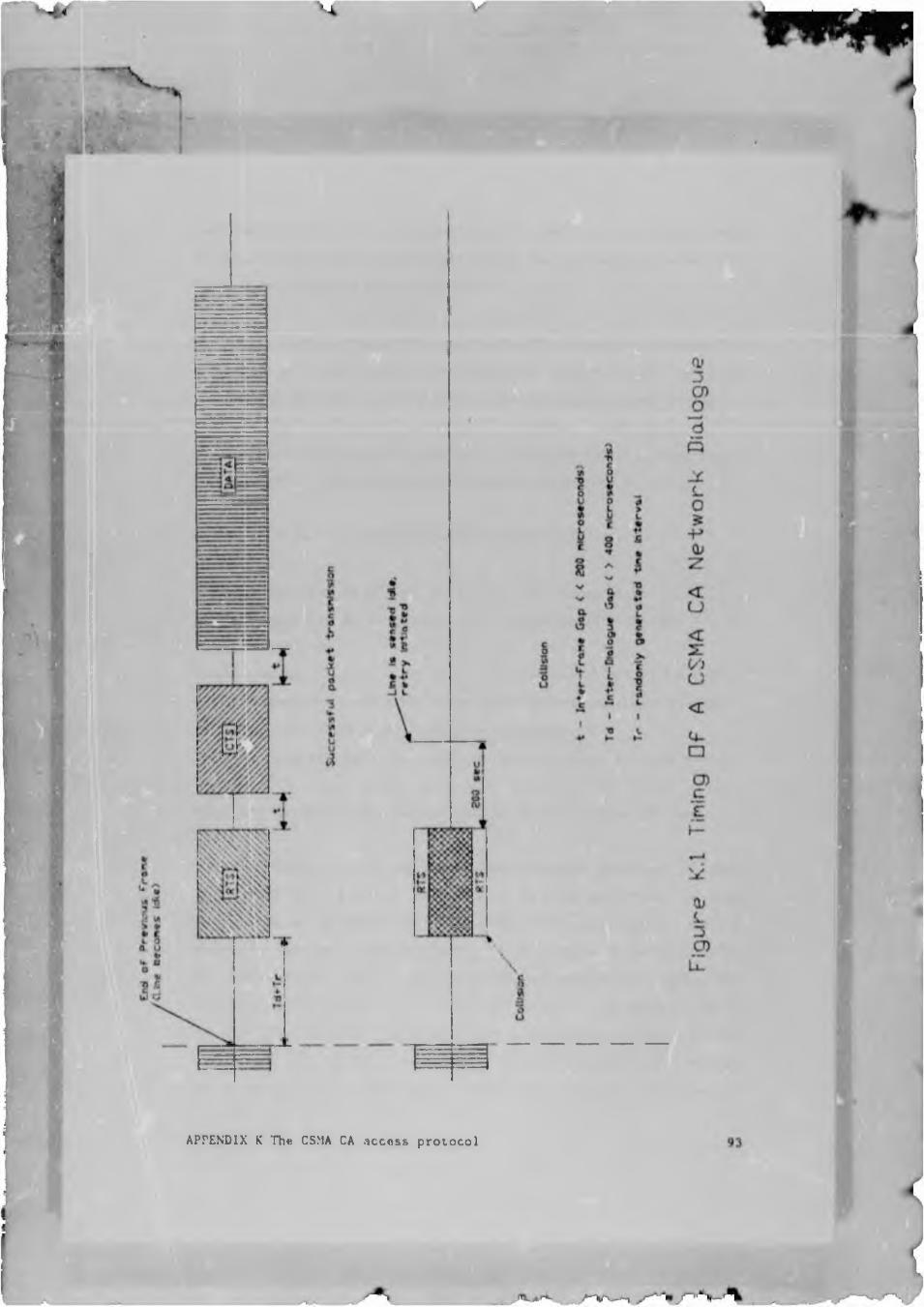
APPENDIX K The CSMA CA access protocol
I
s
Icd5a 5
\
-u
APPENDIX K The CSMA CA access protocol
r£
t♦*5l
1
Ii :
; -t5
h 8
01t
i•o
5TOzt?6XILIL
OJ3CD_odQ
LO5-P0-z
cu
<r5:wu
<4-□CDCE_
CUL3CDLi-
93

The number of bits set in each history byte provides a count of the number
of times the node had to defer (back off) in the last eight attempts. This
is used to adjust the mask as follows:-
o If the number of times the node backed off during the last eight at
tempts is greater than 2, the mask is extended by one bit (up to the
maximum of 4 bits) and the rack off history byte is then cleared.
o Else, if the number of times the node had to defer is less than 2,
the mask is reduced by one bit (down to the minimum of 1 bit).
o Else, if neither of these apply, the mask is left as is.
A typical dialogue takes place as follows (See Figure K1 )
LI)The transmitter senses the bus until the bus is idle for the
minimum IDG time.
L2)The transmitter waits an additional time determined by a random number.
L3)The transmitter sends a RTS frame to the intended destination node.
L4 )The receiver sends CTS frame to the transmitter.
L5)The transmitter, upon successful reception of the CTS, sends a Data
frame.
NOTE: All response frames must be sent within the maximum IFG time.
For nuch attempt in 1,2 a new random number must be generated. If after
32. attempts the transmitter is unable to send the data frame, an error
is reported to the higher level software The access method may seem
clumsy in that three frames are required to transfer on packet of data.
The extra transactions required must be weighed against the extra circu
itry that would be required to detect collisions on the hardware level.
We must also consider the frame format as is shown in Figure K2. The
figure shows the general frame format. It should be noted that the frame
is of the form used <n SDLC links and thus the flags are 7EH bytes and
Al’FENDIX K The CSMA CA access protocol 94
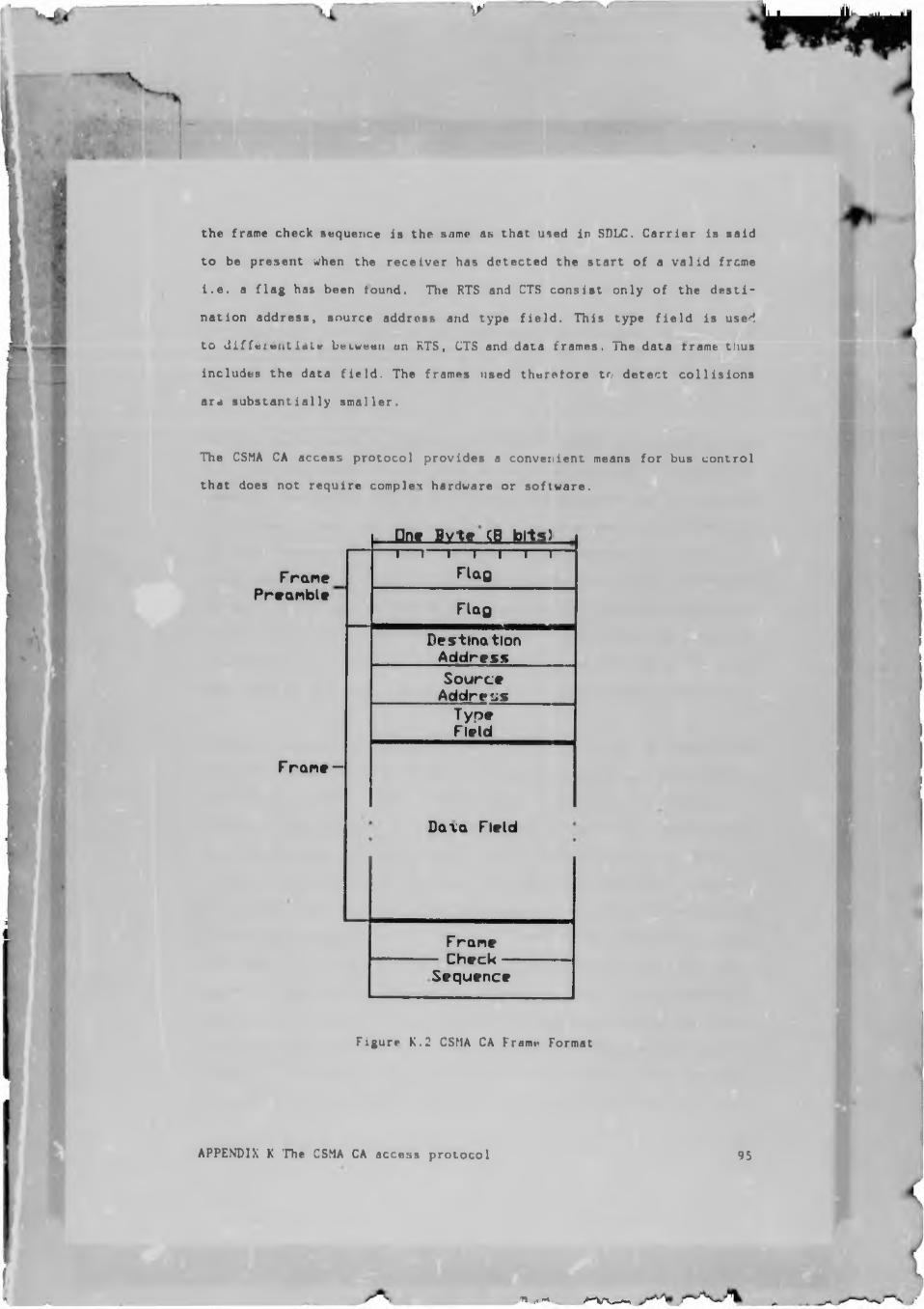
\r>
the frame check sequence is the same as that used in SDLC. Carrier is said
to be present when the receiver has detected the start of a valid frame
i.e. a flag has been found. The RTS and CTS consist only of the desti
nation address, source address and type field. This type field is used
to Jiffeientidle between an RTS, CTS and data frames. The data frame tlms
includes the data field. The frames used therefore to detect collisions
are substantially smaller.
The CSMA CA access protocol provides a convenient means for bus control
that does not require complex hardware or software.
FramePreamble
F rame —
.Qng .fivtg <18 bll9)_i— i— i— i— i— i— r
FlagFlag
DestinationAddressSourceAddressTypeField
Daxa Field
FrameCheckSequence
Figure K.2 CSMA CA Frame Format
APPENDIX K The CSMA CA access protocol 95
Hi. <4 -t. a *v x -*i .
APPENDIX L MESSAGE PASSING ON TRACK 40
The reason for using track 40 for passing messages between the P.C. and
the floppy disk drive emulator will he explained as well as the method
used.
The file server needs to know when the logical drives are changed on the
P.C. and when application programs are selected in the mei u program. The
amount of information that has to be transferred between the P.C. and the
file-server is small and in general only a few bytes are required. To keep
the data transactions between the P.C. and the emulator the same at all
times, the method of transferring information in the form of a sector was
chosen. In the case of MS-DOS this restricts the maximum message size
to 512 bytes which is more than sufficient. Another factor in favour of
this method is the availability of BIOS routines in the ROM of the P.C.
thf.t r.llow single sectors to be written to the floppy disk dri es.
Before discussing the details of the BIOS routine, let us examine the
reason for using track 40. There are three main reasons for this choice.
The first is the structure of floppy disks, the second is a hardware re
striction and the third is time. The floppy disks being emulated have
forty tracks numbered from 0 to 39. None of these tracks can be used for
message passing sines they carry the data. The track number must therefore
be greater than 39. The second constraint is directly related to the
floppy disk controller used in the P.C. (Intel 8272A, NEC yPI)765). This
controller is designed for use in disk systems where the disks have less
than 77 tracks. When a RECALIBRATE command is given to the floppy disk
controller, the head is stepped outwards towards track 0 until the signal
from the floppy disk drive unit indicates that the head is over track 0
(TRACED). If after 77 step pulses (i.e. 77 tracks) nave been issued by
the controller and a TRACED signal has not been received, the disk con-
Appendix L Message Passing On Track 40 9b
APPENDIX L MESSAGE PASSING ON TRACK 40
The reason for using track 40 for passing messages between the P.C. and
the floppy disk drive emulator will be explained as well as the method
used.
The file server needs to know when the logical drives are changed on the
P.C. and when application programs are selected in the menu program. The
amount of information that has to be transferred between the P.C. and the
file-server is small and in general only a few bytes are required. To keep
the data transactions between the P.C. and the emulator the same at all
times, the method of transferring information in the form of a sector was
chosen. In the case of MS-DOS this restricts the maximum message size
to 512 bytes which is mere than sufficient. Another factor in favour of
this method is the availability of BIOS routines in the ROM of the P.C.
that allow single sectors to be written to the floppy disk drives.
Before discussing the details of the BIOS routine, let us examine the
reason for using track 40. There are three main reasons for this choice.
The first is the structure of floppy disks, the second is a hardware re
striction and the third is time. The floppy disks being emulated have
forty tracks numbered from 0 to 39. None of these tracks can be used for
message, passing since they carry the data. 'Die track number must therefore
be greater than 39. The second constraint is directly related to the
floppy disk controller used in the P.C. (Intel 8272A, NEC vPI)765). This
controller is designed for use in disk systems where the disks have less
than 77 tracks. When a RECALIBRATE command is $i\en to the floppy disk
controller, the head is stepped outwards towards track 0 until th jrutl
from the floppy disk drive unit indicates that the head is over track 0
(TRACKO). If after 77 step pulses (i.e. 77 tracks) have been issued by
the controller and a TRACKO signal has not been received, the disk con-
Appendix L Message Passing On Track 40 96
x r g y
[roller indicates a fault with the equipment [3]. This is not acceptable
and therefore we cannot step further than 77 tracks from track 0. The
permissible range for the message passing track is then between tracks
39 and 77.
Stepping between tracks is a slow process (of the order of milliseconds)
and should be avoided as much as possible. It is an advantage therefore
to have the track used for messages as close to the data tracks as pos
sible. Hence the choice of track 40.
The BIOS routine for accessing the floppy disks is an interrupt routine
viz. INT 13H. Various parameters are passed to this routine via the reg
isters of the 8088/8086 CPU of the P.C..
The parameters are as follows [7]
Inputs: AH = 0 Reset disk system
= 1 Read status of disk system into AL
= 2 Read desired sectors into memory
■ 3 Write desired sectors from memory
= 4 Verify desired sectors
= 5 Format desired track
DL - Drive Number (0-3 allowed, value checked)
DH - Head Number (0-1 allowed, not value checked)
CH - Track Number (0-39, not value checked)
CL - Sector Number (1-9. not value checked)
AL - Number of Sectors (Max = 9, not value checked)
ES : HX - Address of Buffer
Outputs: AH * Status of Operation
No Carry - Successful operation (AH = 0 on return)
Carry Set - Operation failed (All has error reason)
The message to be written is assembled in memory and F.S is set to the
segment containing the message and BX to the offset of the message. The
Appendix L Message Passing On Track 40 97
/ • •> W
required function viz. write desired sectors from memory is chosen by
setting AH to 3. An assembler program segment will be given for the sake
of completeness.
Note: It is assumed that the message is in a byte array called BUFFER
defined as
BUFFER DB 512 0UP(?)
The program segment follows:
MOV AX.SEG BUFFER ;LOAD SEGMENT IN WHICH BUFFER LIES
ES.AX ;INTO ES
BX,OFFSET BUFFER ;LOAD BUFFER OFFSET IN BX
MOV
MOV
MOV
MOV
MOV
MOV
MOV
MOV
I NT
AH, 3
DL.l
DH.O
CH ,40
CL, 1
AL.l
13H
SELECT WRITE SECTORS FUNCTION
SELECT PHYSICAL DRIVE B
SELECT SIDE 0
SELECT TRACK 40
SELECT SECTOR 1
WRITE ONLY ONE SECTOR
CALL BIOS ROUTINE
The floppy disk drive emulator need only emulate this one. sector on track
40 since this is the only sector that the floppy disk controller will look
for.
This method is an effer . ive waj of transferring the required data between
the P.C. and the emulator and file server.
Appendix L Message Passing On Track 40 98
APPENDIX M THE MS-DUS DEVICE DRIVER
The device driver creates Ingir*! drives on the P.C. as required by
the network as well as being responsible for passing messages on track
40 to the emulator when logical drives are changed. This file is called
up during the booting up process of the P.C. and forms part of the
CONFIG.SYS file. Various criteria for the structure of device drivers
are specified and since these are standard they will not be discussed in
detail here. Only the important features will be explained since the code
(later in the Appendix) is well commented. Numbers in brackets refer to
offsets in the program. This is the left-hand most column of numbers in
the program listing.
In the device header, th« constant DRVMAX (OGOA) corresponding to the
Name/unit field in the standard device header (8] is set to 24 by the
INITialisat ion routine (0650) of the device driver. If fewer drives are
required the 24 can be reduced. MS-DOS assigns the letters of the alpha
bet , starting at A, to block devices such as the disks. Hence the standard
two floppy disk system has drives A and B . Subsequent drives are assigned
the letters up to Z. If more than 24 drives ari requested in this device
driver, the drive identifiers bee Mite the ASCII characters following cap
ital Z in the ASCII character table. This makes drive identification
aussewhat difficult. The remainder of the parameters in the device header
are ' e pointer to the next device header, attribute of the device, the
pointer to the liev'ce strategy and the pointer to the device's interrupt
routine in that order.
DRVTBL (0008) ontains a number of pointers to routine to be called de
pending on the function required when the device driver is accessed. As
can be seen from the listing « number of those point to the exit routine
directly si net. these functions are not supper'.ed by the device driver.
Appendix M The MS-DOS device driver 99
• * * * * *
The EXIT (0077) routine by which, as the name implies, the device driver
terminates, is responsible for returning status information regarding the
operations performed, to the calling program. The most significant bit
of AH, when set, indicates that an error has occurred. The least signif
icant bit of AH indicates that the operation is complete. If an error has
occurred, the error code is returned in AL. The number of su i sful I/O
operations that did take place is updated before the mach, tate is
restored and control is handed back to the calling program.
The MEDIASCHK (008BI routine is called by DOS before an operation is
perf:rmed by DOS on a logical device. This is necessary so that DOS knows
whether this data relates to the actual media in the logical device or
not. If we consider a floppy disk system where the medium is removable
the information in the buffer may be from a previous disk because the
media can be changed between accesses to the disk. In tha case of a hard
Jiak which is not removable we know the buffer will have valid informa
tion. This media check can return one of thrae values to DOS viz. The
media has been changed, the media hasn't been changed or I don't know if
the media has changed. It is obviously an advantago to oe able to say that
the media has not b«*en changed. In the case of the emulator unfortunately
we cannot say that the medium has not changed because a floppy disk may
be mapped out by the file-server for example between accesses. The device
driver therefore always responds with I don't know if thr medium has been
changed.
The BUILDUP routine (00AB) generates th required BIOS parameter block
according to the given media descriptor byte. The routine usually gener
ates the parameter block for a double sided disk with nine sectors pet
track. It is possible to have 8 sectors per track and a single sided disk
if so desired.
This routine is followed by a number of variables, the first of wnich
records trie current drive , It may be recalled that both the device driver
Appendix M The MS-DOS device driver 100

in the P.C. as well as the emulator are required to remember which was
the most recent logical device, that was accessed. This variable performs
this function and is initialised to a value that would not normally exist.
This is done so that as sc in as the first access is made to the one of
the logical drives, a message is sent to the emulator. The remaining
variables store temporary values during the actual data transfer.
When DOS calls a block device driver i.e. a device driver for a dirk or
similar system where the data is stored in blocks, the request is in terms
of a logical start sector and a number of sectors after that, that have
to be read or written. DOS also gives a Transfer Address where this data
is to be transferred to or from. This method of requesting data is useful
in the general sense that it is not device specific. It is upto the in
dividual device driver to interpret exactly where on the physical device
being used, the data must be transferred. In this case therefore we re
q u i t e a start track, start side and starting sector on the physical de
vice. Before the calculations are done to find these parameters the
current logical device must be conveyed to the disk drive emulator. In
the SETUP (0135) routine after the jump is made to INRANGE (0147), the
current drive is compared to the requested drive number. If they are the
same all is well, if not a message is passed to the emulator via track
40 (See Appendix L). The message itself is inserted at this stage into
the the buffer called TEMP BUFFER (0450). The maximum length of the mes
sage is restricted tc 512 bytes. The contents of the message itself are
not important as long as they correspond to some message format that the
emulator will understand i.e. the emulator's software and the device
driver can be modified to send and receive message formats as m-'.y be re
quired.
The message passing along with making the physical drive B in all cases
takes care of the mapping of all the logical devices into one physical
device. This is followed by the calculation of the physical location of
Appendix M The MS-DOS device driver 101

the data required from the logical sector specified by DOS. The number
of sectors to be transferred is stored for later use. To calculate the
starting sector the logical sector is divide by the number of sectors per
track. The remainder of this calculation gives the starting sector between
0 and one less thai. the number of sectors per track. This value is in
cremented and stored. Th quotient of this calculation is then divided
by the number of heads on the device, in this case two, to determine on
which side of the disk the data transfer begins. The remainder of this
division thus gives the head required, while the quotient gives the
starting track. We can now commence the data transfer.
The actual data transfer software has to be inside a loop, the reason for
this being that the maximum number of sectors that ran be transferred by
each BIOS call is in this case nine i.e. one whole track. The number of
sectors requested by DOS may exceed this value or wo may have the situ
ation where only two »ec.tui s may be required but the first o c these is
the last sector on a track. Two BIOS calls have to be made in this case.
The loop counter therefore is the number of sectors that hive to be
transferred The loop performs the following:- A retry counter is reset
for each I/O operation. Four retries are performed for each operation
before an error status is returned to DOS. The i'KF.SET (03C0) routine
checks for when the end of a track has been reached. If the track end has
been reached and thi* operation has just been performed on sidv zero then
the side is changed to 1 and the physical -.octor set to 1 i.e. the start
of the track on the other side of the disk. If the end of the track on
side one is reached, the track number is incremented, the physical sector
set to oni* and th*» sid# set back to zero. The first time this routine is
called, none of these situations will arise since the starting parameters
will just have been calculated. The parameters for the BIOS routine (See
Appendix L) are loaded and the routine called. This BIOS routine returns
with the carry flag set if an error has occurred. AL returns the number
of sectors that have been transferred. Taking initially the case *..ien
Appendix M The MS-DOS device driver 102
the routine returns without an error, the transfer address has to be up
dated by an amount equal to the number of sectors transferred times the
sector size. The segment register (ES) is constantly updated to prevent
the offset register overflowing. The transfer address is not updated by
the BIOS routine since the data transfer is performed using DMa . The
correct value of the transfer address must be obtained for subsequent data
transfers. The number of sectors still to be transferred is updated ard
then the loop repeated until all the required data has been transferred.
When an error condition is returned by the BIOS suitable error handling
has to be performed (BIOS KHROR). The exact cause of this condition is
returned in the AH register If a DMA error is returned (AH=9) it is
handled differently to the others since it is the only error that may not
disappear if a retry is attempted. Since the cause and handling of this
error are somewhat different tc that for the others it will be discussed
later. The retry counter is d.1'-rodented and the operation re attempted
until the operation is either successful or the number of retries has been
exceeded. In the latter case the BIOS error number is transfotmed to DOS
via ERROR EXIT (0292)
Th* Li\4 error results from a hardware design aspect of the P.C.. The DMA
controller used is only capable of addressing e4K of memory directly. The
P.C. 's memory size is 1 Mbyte and for this reason an extra register has
been added to accommodate the extra memory i.e. the DM\ controller son*
trols address linos AO - A15 while the register controls linos Alb - A19.
The DMA error occurs in the following situation, DOS may allocate a data
transfer area that causes the address register of the DMA controller to
overflow. What we would like to happen is that the extra register be
incromnntnd automatically. Before commencing the data transfer the BIOS
routine chocks for this situation and if it will occur the or or is re
turned. The following procedure is then adopted: the number of whole
sectors that can be transferred before the overflow occurs is calculated.
Appendix M The MS-DOS device driver 103
a- ..V - -

A request to transfer these sectors is then given. The sector in which
the overflow occurs is then transferred to a temporary buffer
(TEMP BUFFER) i.e. a request to transfer or j sector is given vith the
transfer address being that of the temporary buffer. When this transfer
has taken place, the temporary buffer is transferred byte by byte to the
original data transfer area. The remaining sectors are then transferred
in the normal manner. A similar approach is used when the problem occurs
with a disk write. In this case however the data is transferred into the
temporary buffer before the BIOS routine is called.
IN1TAB contains a pointer to a BIOS parameter block for each of the log
ical devices. The 1)RV$INIT routine is called to initialise the device
driver. The 24 that is loaded into AL in the first line of this routine
is what must be changed if fewer device drivers are wanted.
Appendix M The MS-DOS device driver 104
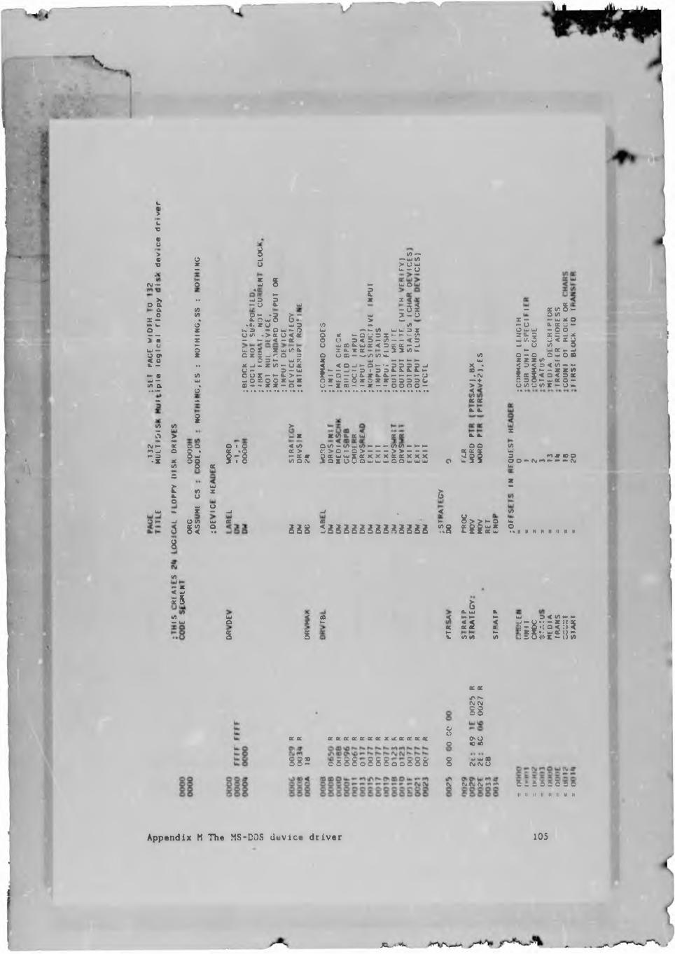
L>uV5> 8 v)—« O -1 — UJ v>T9 Z U > U UJ«• Ue ■* O
CU — O 5 § u- UJ ot-
o d M O Z w2
X • • w b p X I <
a (/> - 5 5 — « v> B —
= 2 "I 2 5 J 5 5 T 5 i - “ %- 2 2 *o— u. o .t. Z L) W O W — V) — U & Z U -O Z k. 3 — O W — O W — — VI UJU. 3 T O uj UJ — o o — O v i « > a. O < * O * « - O U 3 S > - f - - W Z - 3 Z = — *3 n X — — w < — X O O 3 < 3 — IT < 3 U V. 5 3 < X yu — u w m e L u x < 3 a c a c — -J — o iA Ow — o u. o i Zwiea r a. x ac — — S x ia u. — — x - -iO O' Z C Z $ U < O 3 O O CO — — IAIA u. <A 0 - 0 O UJ O CD< O 0 3 — w K Z w — — — — W Z Z Z I A u .(L - .. * U - Z I A — U * < < 0 -1— O — • - P P P P - J X • < 3 < 3 <CA — —U - 3 — UJ r — — U — 3 I 3 3 * . x E C — CD ~ X X — - Z Z (A— e ia oux — — a.>- I — o — V&-ZU.& — — — — u •cm X cc x < o < 3 ceUJ — W - i O S o O Z ujZ O Z w O O Z C Z Z 3 3 3 3 0 — ♦ 0 3 0 —ujCCO-v) a . x — z z — o — u — xcd- - z — o o o o — >> uiauiax — O —• • —■ O • * • • • * • • • * • • • • • • • • * * * • • • • * * • • # * • • • • • • * * *% 4^ • •
— - ae oc
o w U
V)ii
a. a.
S( A M >3 > - z z <A cu cc u j a X 0 . 0 .Q. Ou X
fy — X 30 0(0 < V> OCA — <Aw(A — — — <AV> — — — O O Mia -j o © • cc •o oc > r > o — a > > > - - — ccxac —<— 3 ow 5-5 - x » pacujujxexxxococxxx 3 O 5 3 mz op. X * 30 3 ■ O (A 3 »\j "IOXOOO ujw—jO O ujwuj O u. 3 $ 3 0 — Oj — — — — Cu(A O X uj
S Z> w —t S 1 5
< MUJ u. X — J -J . <
o — u o m w x x - 8 > > — g —5 55 ?. 2 2 8 1 2 2 2 2 2 2 2 2 2 2 2 2 2 T.8 £ § 2 ^ 5 °I • •H tt N H N II N H
( A W « e «{ — — — w . 3 < M — —— UJ O i ►—5 5 acH%
>< u § a.H- ►-< < <ac a a.
Kv> </> in m m n
8oc ac ac oc oc oc ac oc ac x a: cr o: oc Os pQ oo ac
8 8 2 0 8 8 8 0 8 8 8 0 0 8 8 8 8 % £ 5
OC 06ii
ru rv Ov m m C t i i C O C CII Ii II I II II II l«
Appendix M The MS-DOS device driver 105
JC.
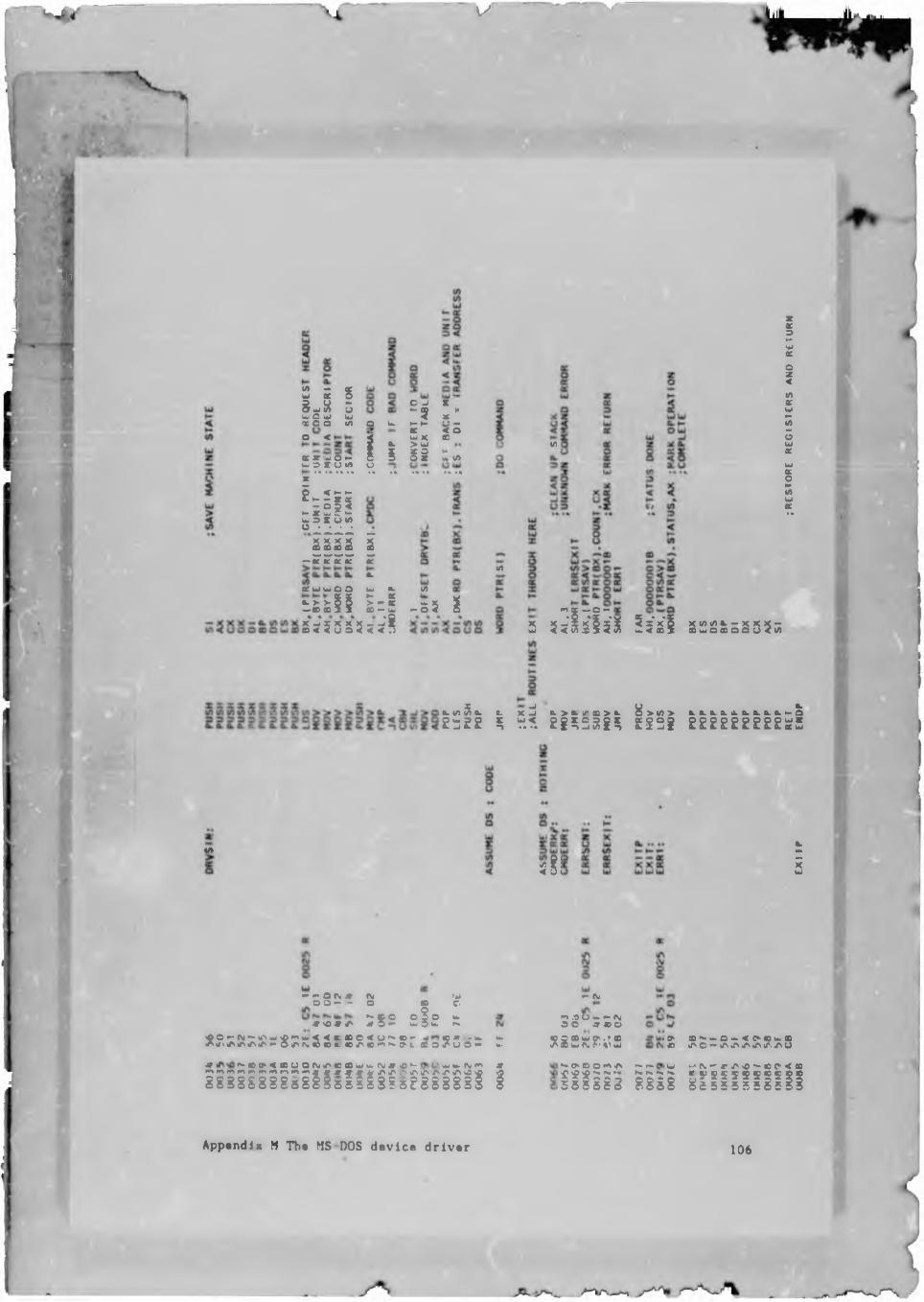
V
:,
V) - ac% j !w O w w ac O o m O u.o < <
ik x w o - 5W 3 t U V> U
O -J 1-5 x " 5^ <SW x CDi II u
T
h il lo • • • •
IIII I— a a a q: ac
a.
0? UJ U< O Q
usllCm CL
s=i£i$355sal
co.55 I
CO
CZ) (
m qc w Q •» i5 3^*15h i h i# $I2S&5§53S
i a. V) $ a. c. x d e. > a. tz> as > a. 8 > i/i > a. a. a. a. a. a. a. a. a.
2 : 2 2 3 :f. 2 1 ^ 5 5 2 ^ 2 2 2 2 2 2 2 2 2 2 2 2 2
v>
s § !
»* »• O f\J X f\J wO O " - o s c►» » O 0 8 0 u.X O X 1A X 5 "■ aj 5 a. fa
~ p O f ( M ’ u>^v()"'a.<<er, C D C < U ~ e - to * V a. a. ^unAiAAir - OiAfvjeea..eiAewfaff-c m o f u o — a.X fa « 9. 4 CD U O (Vi IA C CD W a M X 0 ^ - aj a. (\« m X pnmmmfiiammmfaf X X X X X A A . ‘'irv^AAiAO'0 \0SSSgSgggsgllslilglsigggSil i
*- fu"V 3 O a *• M3 C X » o
X g E K P ^ S - a eofaaOaxcaeaej *> lAO iAifV i/M?. AO) fa o. CB O fA a fa fa w ►-• (V «“ X A O "a C C* «t 60
imils Sill ililiiiiiilAppendix M TVie MS DOS device driver 106
RE I
;RES
TORE
RE
GIST
ERS
AND
RETU
RN
EX J I
f EN
OP
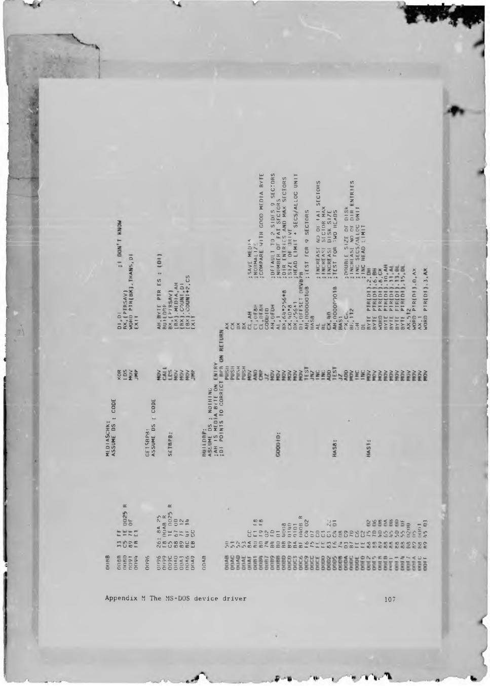
a</)
2i ”(Z) QC o: ►-C-
— Q.O O H.
zsiE
(/)w
o:
to oX — *< Q (NJ
> < — —U- O- O' — C O^ r - X O 'J>■ o ...
- - X X X - X 3 X ££ 20 CD X^ £D CO —- w W
w toX Kto —> c X z to toCD ► *
u O XB
X
< w u u H Xto w O ua to to -J X zX OS X X toX o X < X X frto — to — < x tO ee X —g x U X to X < X fSl c — — z8
O x— to_ uC x cH «*• — <
X to u o c ac to z to u - c = x X U H< X o - x o o o —X Pd < > 4- to u to o - Xto — O uw — 3 x C —z < -J — .
<■" — - uty o U K *- O' z to a kXiN o X ” X X X X X x to X to Ot— o to tr to o to u <x 3 x -J X Z O X X < < < X X < X X< < X x X x X to Zw T x < X x O H X X X * - CC X> X X - X X N < to u u u to a u u u< o c X X X Z Z Z X c z z zto X u o z o to X X 1- o — — —
oo
X • • CD
X COc o CD
5
X I Xoo oo c a < c o a o —
X X X X ~ -J -J O X* -J < U X O C U O O < <
so »-U> f- wJ(\j 00 4" to* * VOzr O ifvu. sc C Aj OX X X - X O Q C
1O OO• toX < _ j _ j < X < CD
gI• C 1 PU
• • • C tfs (\j sO 00 O f'l
o o o o c o o c oX X X X X X X X XH- ►- N- *- k- *—x x x x x a. x csj x x
•- o - •to • • X < X * X - J > >
WWOWWWWlTvO — C X h- — • X • Xx . c x - i > > o > > > > x o x ocvffit5Qccx5fflffimcD<5<^
llll > U (0 > > > XX ffi X X X X— X^tOlOtO>CX > > > > > > ION O U O to Q > U U > > > > > > > > > > >
w wQ Qo ou oM
at to toZ Q .. QX w 2pX w £< X £ X X- 3 cr 3 CDo to fr- tox tO x to IaJX < o < to
z uU O U , Z X — w X
2 : 8 O CO
z < 2* Q to to X ►- • • c r z
S LU to o c r - x
— v/) X —a < < QQa %< to<
X Xtn
tn x c\ jO x X D O CM 3-o o £ O O —
< <00 o X r- X X UX — ^ x o *- SO ^ ^ 0
rn CS CO SO CO lA £ Os U £m u co x c\j X u £ £ £ X
£ £ C #- a- VC sO Os U O ^ vC O' £X CD £ OS Ch Os 0s Os Os < < < < <o O c o c c c c o c o oc cc c c c o c o c o c o c o o
(V so oo < X X U . roXOO 00 C\J ■'J V»— u . C O C ^ “ X O r g O
C & O C C cU*-OsPuO — o — — 3‘ ^ O r ^ » - 3 ‘XOsUsO(MLfsOOirxJ,' O ^ C V w XiO UUJu-OwCiTCCCUOOUUOCU^UU'^^crsO^u'SkOX c XCC Xl m < CC~~OC 00'<wk.\0 iAk-. UfrnvO ror uJLuflOXysoCOCOOaOCOOvaOOv L^j>Lnu^ooccoo^xxxxmx — -.-.oou.r-.offi«- cotoocooocxccxxxx
~ ^ < u u.
Appendix M The MS-DOS device driver 107
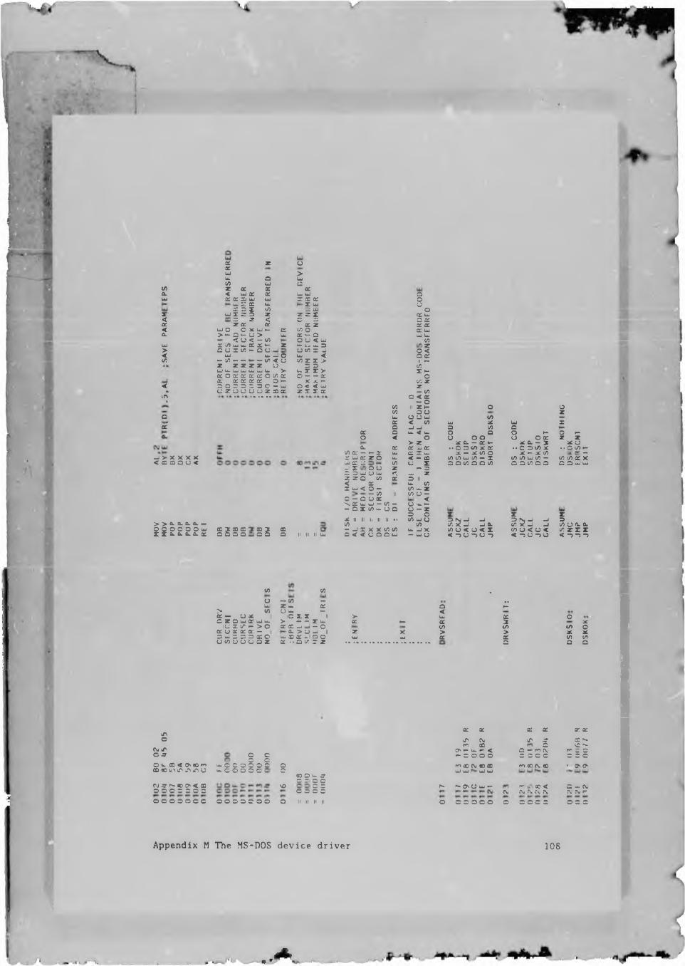
X z OXw >u . Q wto w t t
to z X X XCL < UJ X X W UJUJ X X X UJ UJ X X X
— n x Uu Z UjX 3 z co 3 LU
X w r z 3 z z z z< 3 Z < C 3X Z X X X z< w O O x UJ A X to oa . > • - o — u > UJ X — o
< U < — to O CJ < u iw X tO W W X X u- z » - u u . 3> C U X to — o u CJ CO 3 J< w UJ - o U <to — uo — — — i o < C to z z >
z z z z z O 3 3w u . UJ UJ UJ UJ u. > u r r >x o x x x x o t o x o — — XX X X X X O H- X X • -
< 3 O 3 3 3 3 0 — w O < < UIC Z U U U U Z 3 X z r i. x
l f \ • • ft • ft * ft
oof
-J > X X X X < 23 CO Q U <
> > a. a. a. a. ►-
£ i £ £ 2 £i 2 2 S§: igl COQ M II M UJ
§a.v) e: —
r u i c: w c: u
| l sX U» <0 — 0>vo: u-'- o rx n n (/)- -J Xo < <
*- Xz - o
o uu UJ COIsu ac uJ — to —CO u. U Oll II II ••X X to toU O O UJ
II
§o ac wC X X X X wW L.COE#I —COr H-
oto z z— to
O < X— o
to II Z H O oto oo zUI O CJ UJ </>X < to W X w Xo -J -J 3 (O 3o u- < U. O Q O H O H-< o o oo o ox z z
> z X X — X A X X — i X uX X uJ X • • C 3 V> X X • • C 3 V > X • • o <o *■»u x x ui X — X to o X - X to -L -- -u. < — X to to UI to — X to to w to — to to X Xto U X 3 O CO O O to 3 3 tO 3 3 3 3 WW Wz — 3g U ZX 3 II
u tOt o u . Zt o u —
u ■». 5 E - gV ) UJ U vs u . _ l x— UJ U
3 ISJ U Uv . X _ i - J O . vs o < o < x < - s u - s u - s
X X3 N - I -J 3v s x - j _ j vs u fs. a.vs u < u < vszxx< - ) U -s O < 3 3 - 5
vsow> vsCC — U X I
C Z O UJ X u J u .I U X V — > oX U X X X — I
3 u. 3 3 3 K Oo vs u o u o z
(A
*— to —Z u . XCJ U. —w'OXX_ I > — — Xu.x x - j - oflu > U -I Iw X X . o o x ..o co r z
•*$
3 u<
> w X oX K X 3 X
to t o t o oz X > > X Xw w X X to to
3 3 3
lAo
Cu iAc a-■ ■ ■ ■ ■ § § OU. CO < O' 60 3 u. c C O O O 3- - - u . C O ----------------CDOOuMnVMAU
(\l » 3 «0 o < s 0 0 0 3 3 0 3
o O C :
O O O O O O C 0 0 0 3 0 0 0
X X X X X XlA CNJ tA 5 3 *-m 3 3 C 0s — u - < 3 — m (M ^ 0 o- 0 0 0 3 3 0 0 0 3 3 0
o m 00 OJ 00 3 m eo cm eo t on O'o UI UJ UI UIx o u a-or ocNO o o h- ^ O' CJ w — fr OO < 3 — CMc o c o CM CM CM CM CM CM rsi r-o II II II II o 0 3 0 0 0 O 3 0 0 3 0 3 0
Appendix M The MS-DOS device driver 106
. - A
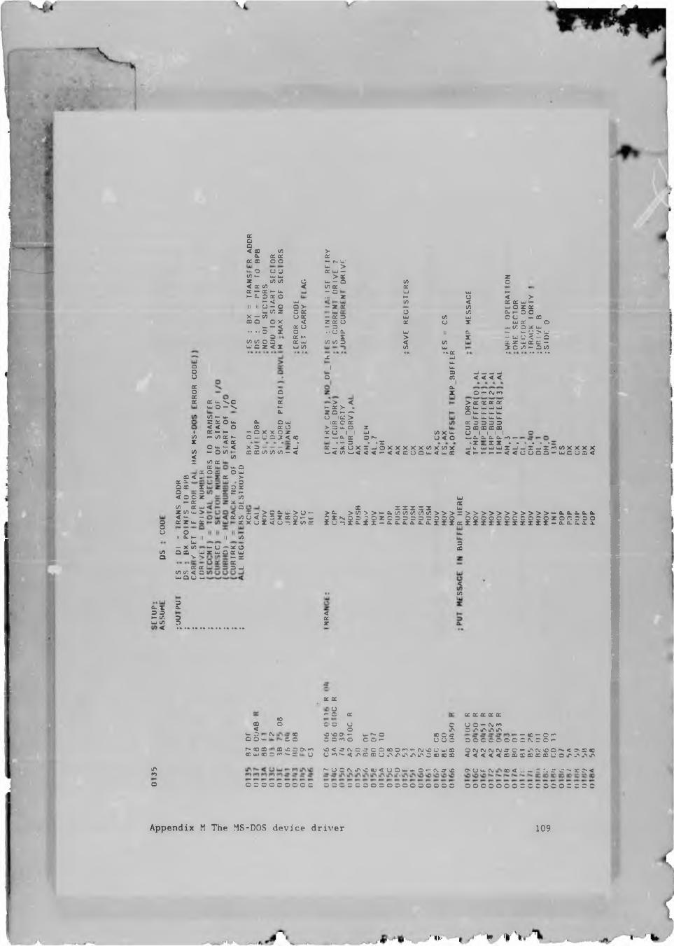
o8<£OQCX
1
COQ
I IU 00 <
IIf)z<A<X
%2) < WWq: a.O X X§ = Ei
M- X (/> X W Z W > < — — X X U. x
QII x k. IIw— X tZ)Q CL —
> >
X X V) to < o w O U —
2
X U. v^c uJ O — tn *- u.ir x o u. < < o x-»-*- to X >“< X O u. •- <— O CO ♦- (/)(/) X XO X X
85< x coX X Xx x o o
u.° u u to — w w X (O V)< X COX — X •— u.H X o x O •— <II H u - o -J to X x — co X o o x
. . . 5 ~ 53to CO c o U.' X X < X
QXh-X
x O wX X o
- Q X X O XO -J u X 5 < 00X X ~ - - z JX X CO CO to — <
>X•— e». u.'U. >X UJ —> x zo uj — O to O< co x X—• O u w ►»- Z H o < >UJ to < X X W k-c > - Z X CO LJ O Z XO X o CO x »- o Oo x - X X w to UJ c U u_ X< z X o X o z w X OX o - X UJ to o X UJo .. £J X w II X h- — c > tuX k- X > z — Ll! o < — cX UJ co to x < to X Z hU X X —W CO CO w 3 O CO M X toX
1•-XUJ
LL.u.
■ • • e m • *
X U -J U -J 1O X < < < <
I
> <H> X > •X Q * - —*U IX >
IX c X > X - Q X X U I I UJ — w x s: or-- - X * -X
Xz
to X U.u < o
L
X - J X U X X - J O X X X X X l O X t O X^,<lOw < < < — < < X U C U J < U J X
o *■“ C\J fO> X X X X X UJ UJ UJ UJ X u. u. u- U.
IU. u. u. u.X X X X X X X X X XU I I I I owXXXXro*—»z zz z * * * • * »x-iL'UJUJUJX-J-JX-JXrncOXXXX < h - h - > - » - < < U U C X — U J C U X <
^ oO UJ
=1 X —COX u-l
< °X to
X
X - ' > C X u - > 0 * - U < C X I X O — u- XUX<UnZt^X
> XwX.
X X X X X X U.> c o > > - x c o c o t o t r t c o > > > x > > > > > > > > > > > - x x x x x
i S S i S i B E E S E S S E E S S e r i i S i E E i i B B E E g g S g SII V)
- u —Z UJ Q X o X w H Xi-j
XX
<CO
5 <Xz
5U. x <NJQ O WUr- ao X 00 uJ 00 O
§00
G OX "sO o 0\ m r*"' ^ X O
X X
u— C X
CO u CDxC <) 0< r-X O ro O UJ ^ O C O ' -%
853v r X ^ C o C . ^ C C o O O f * * ' — ( M v O O U i X om^<ir\xxuiAinmj\i^cooxx
X X X X X
U O — f\j ro O U> J> iTMTn — oo — Of^OOCOOOOC(N.OO^ofucvcvrvj^-o — J>f\jsoc^< o x oo < < < < < X X X X X X U O U ^ - ^ ^ t n
inmo
N-OOf^J>cou<uCuju-o*-c\icrvC o u u. ou oo < . — rrwjro^5rr'<o o o o o o o o c O O w C C O O S O O O O O O O O O o o o o o o o c c c c c o c c c c
Appendix M The MS-DOS device driver 109
/Ik-' v -ir>r
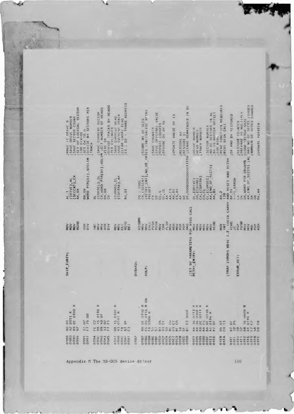
v
7)
COX 3 3 3a: cc to o w O UJo w Q < « > oc 3 3Q. oc < UJ o QC UJ Z —j »- — > < <o O UJ X X o H- =3 CO < UJ 3 Q -J c ca: w V) >- X o u < L. -u UJ CO or UJ c. _w z m QC u > < < o co q: < ft: Z u. W X — UJ00 cc3 O UJ u. cc w ft:< CO u > NO U. uJ — u. cr o X — Nl CO COs O -J #— to o % K -J z w w QC O Q O -J U» — Xu. =)o < i; (O < to CO -JUJ Z o: co z u CO - 3 CO L> w> z o w — cr x a:»- u- cr QC< > UJ cs: ft: w cr x o < w z X UJ >cr O c/5 z UJ O UJ iff z > u. _J UJ Z CD < uj cr w re o uj — o X -5 X tO X za: w O 8S U- CO < 2 UJ UJcr o < 3 X - X W Ui CC X K- U. k- o c oc > O > o: I o: z a: crQCli z o O < < ouj X CD X 3 u u. ox X O — u- 3U - h- CD ft: 3 »- — o: rj.< o #- 3 o a > QC Z X 3 z uj 3 y; z co CD U C 3 CL*- a:Uj > =2 Z X - 5 3 O z — o ft: w w Z 3 Z CO X O 3 —- a (/) c. — X w U O UJ > u U Q z O o UJw w cr QC w z X — U. o Q X X 0/ c U.3 O O C X h- Q U CC — Q K- o o > U X O u. (O X Z O < Z u>W UJUJ — o UJ LU o — W Uj< UJw < < — < >30 *- O — O CO < *- X 3 X <x > > oc >< > c a: > ft: > > UJ o > > > Q to to LU - < < u x < o CO w < to x 3< < < UJ c U — QC < •*Uj — uj < < -J CO — CO < < O & UJUJ _J ft: w ft: UJ o X O U. — UJ X o < X£ 00to in u. c/) n h- CO N O a. to COU W CO Lw to toQC O 3 QC QC •» 3 X »- CO Z X w_ x X 3 X X _ % Z 3__ QC 33 • • • • - • * * -Jz -J *— > <Q 1 X-J Z Xo O UJ x —■UJ 1 O to X > CO</) O i § h-o Q 5SO w z wX -JQC ^5 o '—CO < X to-»u o Q h- U» i* o - - X U 1 X #- 1< - CL Q % w 3C Z o U O QC W u. H O X u.a: Q U O o > X h- co o W X ou- »— O Q — X O O 1 o - % ft: X I CO X C 1w z CL W QC o ft: O UJ > H o C 3 3 3 O w LU X c>U X X coox = co o: uj -J CO — X o 3 U O -J U Z — X — 1 o z Xu o Q O 23 0 Q: ft: Q • • w »— CO ^ O UJ o < c O CO 3 «- <-a: uj - ft. 3 * . % 3 • UJ u -c-j o i U U X X X o u X to x QC or x — - X X X 10 X -JXXX-JXX X rr>z X X X X X X X< — o — o o u 03 O U O. u o u o < < < UJ < O O 3 3 O U U < CD < < x c O 3 3 < 3 3 3
> > > =IE
oU > > C £ > > > U T? i § § 5
— X X XV)>>-JV)V;>Q:V)" 'i£S"_
5tZ)o
3223; :BaZ>S>0-E S S E
a-QCC>>>>>>lZ Z ± i i i £ 2 2 $O
(/)a:
>«:AC<oxuw5$ CL ( / ? > > ■ • C. O
gE .%%2 2 S E ; 2 S
Utitr
o
X(Z)
QQCXOQC
a. h-
>tr
(/>QCHoc wwu o:
Q. ocrq:
X X X3 o u.
X o C XQ u»m o o oo o *-w (\J iT \ Cu NO 3 ou f- NO *- U.oo O 3 N u — a- 3 u. — O 3
OCVIOn C\j t ' i h~ uj x x m r- X ro X roX < 00 On fO u. u. on oo m u. 00 < — 00 (JCD 3 C J? iTN N. < U O m ir h- X uj u. »— (N.00 00ON O' ON ON O n O' < < < < < < < X CDo o oo oo 0 0 3 0 0 c o o o c O
o NO o — acco:ui o m coc a- U.OUi 0^0ou o
ft: a: o: o:O O t- *- QCO • - f * - r -O C C O C-S
<0 vC uJ 7s Uu u .uj — m O u, o O QCCnOOD*-^- — CU^ujOO^-r-COUhiJu iAftlQinoCOaOkrMACO < < CD < < •— n*
OC 00 03 00 00 < ao
CM ro O fzr cod u
u. if\ OCl
ccC QC cc s-sC •“ C\ *•— O U- u.
oo iTN4n50<-.. 0— O —C O O O O C O O
Appendix M The MS-DOS device driver 110
<
,n [fljv .f -# , -*W » > ■ #11 n 1
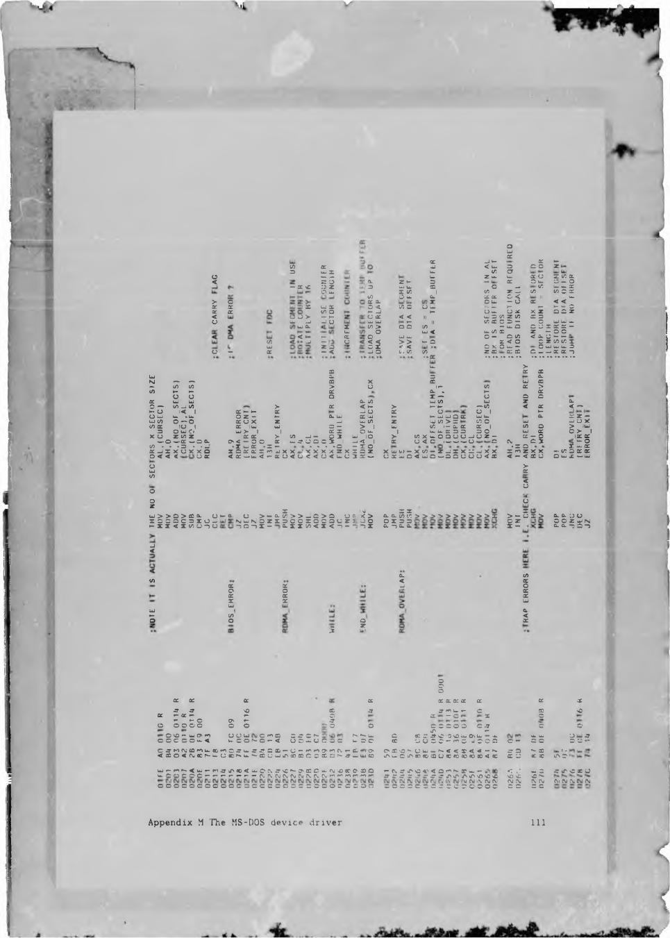
$
>2Zcc<o
t/>3— % \C
o££o: is
O -(/)wcc
o u >uj —Jw a.< Iu
5 xiiO uJUJ %1Z) o— h-- u
isXwCLO
a.J340IIu irLU W
I !
owQC
IT - j k- a: #-UJ < w 3 c o Zu. </> aU. Z U- UJ X u z co cr
Z u- © CL o UJ 0 — 0uJ W CD O -J co w w. a:Z (0 1 C/5 z -J CO co © xO w. ft. cr cr G < II W
I O uj - O a: < <5/5 C U Ui >- — H t- ^ - ©
K O u. O jT X z © © z< < H u. © I/) Z (/) CD=3
II CO CD C © — O uj u- —a 5 'S> — u- © © o x cr c: -
w < u. CO CD Z — © ©W UJ o - O CO < o. O — —> > - O X < O © Z CO CO x< < © X O Lw — O LU UJ U. ©0/ t/5 CZ) Z CD ft! CD © — — X X -5
■ •a:u. >
CO X Xw X © ft.N — ^ X X X w X— co to > o If- CO X >CO k- *- X X % »- Xo o a z — O © ©X U* UJ ft- iO W CO w z© — CO -J CO > X < H > h- U- — *C0 < X•- O l < 1 X *— >— X u o X o O 1 HO UJ u. .u. O z - H- X UJ X -u H— u- UJ UJ © X w u. CLuj CO 0 — 0 X O X z -J W CO z W CO > X CO O wCO X IO 1 X IUJ w © — > 1 UJ CO 1- X X X 1 CO ©© O UJ o UJ > 1 1 X X ou. 1 u. u. s: © © © O UJ XX O Z CO z 1X X > co -J- O 3 UJ IO > C O X u - O Q O O - J O Z — X - o
—» © —' X '— © f t . o < - © © X w jy o o e S i -J < 1 X U < O 1 w *-*’ w O o CVi C 3CO • • * © * • —< -z UJ X * X * - • •• • »© - T O • X ©X - J X X O X X O X © X X X m w X X x x x x z x x o z X w v; — X t o — Z - J X X l : - j x x X ro Z X X© < < < O X < X —-UJ < » - X 0 < 0 < < 0 < U - U 5 X — O X UJ © < U J O W © © O U O < X < — < X o
Cl < —
X z -uJ U X > IUJ =&=' r 3 §
— t/5 5 cc ocQ Uj X *— _Uuwtz>01UJ > > O > CD Q. o IOOCC3ZO-- *-ZZ<Z(/)U-)U
u- ft X INU > - c - i c > > _ . C > Q O =- < > a.
m uin. o r r = o o x o c o c r r j o o-5 a -! I - o- I I 1/5 < I < -5 — ~ *2 I o.X X 0- Ifl tt 1 3 =
- 5 a. a.
> > > > > > > > > > x
>cr
5_Lo
>- 5 x > $ E
a. o-uoO C Z w Nc. c. — o -)
_J<
00
wh-o
§ACXw
V,'o
Koo:%
5 §
CL<UC/5§IWa<a:
cco
cc o:zr ^»- oc «-*— ^ oo o o o
O <0 uj f> m O O C C O u . <
ccNOs i
u u tu c m co u. © © r- © *- <
CDOJ3-:o© C C N*N-U O u.' u c Q C U. ©
C^y,MfMtorou.oOrn©jyuJS, ^ l © C D f-U — ^r- )0 '^ (X '^ -C L f <cD©<ruoor^u-uoo^u.*^cD{jujif\oocDc:©x©f^jy-.v
ttcroUJe>0\ * co
ccc
Icr s. o: cr <r^ fO U. r- ©
CL — O CCc© ©5© c rtT- «-OC r^ 'O 'O O U -O ^U J — v*.uoeo - w o . u o o o
Lu^ ror>~.<uj'— r»l^ru>aD<u,©f\^rNC^-a\Cr:C^L.CVvDCC0-'2DQu . © O C © © » - » - » - » - f - » - — (\l fV(\;fM(\ir>jrvC\Jf\jr#l^'rorr'enfv‘
© 0 © © © 0 0 © © © C © C C C © © © © © © © 0 C C C 0 ©
O 2Cs0 ,s*-Uu;w.r -<< X <. < — kA^©kf\0D0DCDUCOCC0OeOaD<QC
- ( \ ^ > r N O < i r < © ^ ^ c c ' i -5-r^r.r..T^r^reJ>^ irNsr>sD\C . , V V cv X CNj f \© o o c c c o o e c o o o o o
X XX so©© ©
U» w o ^© — c © © © -C 3 ^ X f - Ufx U OC X LT\ ©
< V W 3 ^ ■ ^ o x ov£> C c cu rw CN. rg c\i M X CN© © © c
Appendix M The MS-DOS device driver 111
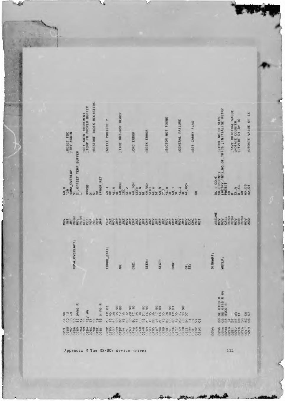
X XX o o o oO m © co <\j — x co «- m ©X » * * O » • uj • * O • »O * •X r-> O Q X cr x x - j w x x _ i w x w _ j w x w _ j w x . ; _ j w x u . u w _ j
< , - % ( / ) ( / ) u x o u u j < t z < © < u < r o < ^ < s < v ) < © < u < m < o < f f l <
>>-c.^>v:©CLa.w © -j
g = 5 5
(
— UiTCJ>Ui/M\lSI.)ir3"Ui/N'»'~Uir'«e3Uin»'mu O i»-30"ii-C3K»-0DfN<>*’0 3 * * i ^ C C 3 ‘— C 3 C C
^rcacc^ujr-uwwuiova. o^cxoirisc 3u>3eD3iri~{SOirc,so^'oec«c'JM>m roui- ir>cDJM-. .iAu>iAuj er-.c«-e’~ai~eor~x««je'~aitioo"~eitiT~-eitia — «.i/>oui o rw -»if. w »< < u o uj ... (\nr .o<u — w'60'XQr',i>r',~<o — — »~-e>ewc. — <Mw'~»exeeTxe<ree c>.oc t>CM3'<<<*i< < x b s ix x x c u o u u u u £ 3 0 c (\jPjfjPjtS/<V''JfM<\jPj(M<\j MNlPj lX(\ l , ,M<M(Vfj(\J(NirMru(V(\jrj(\irj<\u(N,fu(\J(MVU<NirjXej(NjoreocoouoooDre o o o x o c o c c o o o o o s s o a e o s a c c o c a o o
Appendix M The MS-DOS device driver
t/J X Cz —
a u uir x w
tnxxxx--j-xx^
5 ^ x x r — rvjfjr'-o C = Z 3 — w — u. — -<w
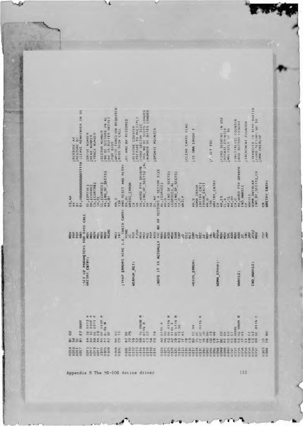
Xw a a wo X L-U.X _J w a > < < w 3< W a a w o o (O X C Oto w w a w w a W X XX Z u. X x — w a XH O X *- N to 10 < z Z O w 2 a.a O Z -J x w — X \0 3 Z Z W 3z X to 3 W to - 3 to u m. w u. uj o - aX X w X X — < w Z T UJ V X u - o X< w X W x a M- o x a x to x z > O z z > u O X xx - £ CO MJ CD X — u. u o o o — x ar w 3 CP w X - c << L X X 3 U u. Z X X o — W u. O x X o X C to o *- — wX 3 3 3 z u. a to a to CC u o o X < w a o u > — w z X U Xu w Z 3 Z to X O u. — o W W — U W W ak. W3 X W Z X - e a x x to o x w to w x < W z U. If >O 3 > W X O W to CD w z o < Z u. w X ■ to — to G< > o o O — - to < - x a x < < O w a < - N. x Z 3to <o Ui — < < u x - o tO w < t0 Z a to < ►- w - a u < < <— --1 X w X w O X o x - — w X O < 3 X w to o c a z a z 5 5 #X X .% a x - to Z X u. 3 x a x x _ r z a o w x z — < —• • •••••* • eX w
> <X aX w Kw a N ^ ^ ■ Xto X >10 — to to > Qhi X H- to w H XU e a o u o aUJ z u X w w > X to
< X X to O to w to x X < *-U 1 5 w i »- O l< 1 X L- H H- w w W Uw a x w u. H X X U . U u j u. »u. O z - z x _ X UJ> X »- to o — X o W to 0 ^ 0 X u X w W 10- X X X to w a i to X IO 1 X IW | a x > 1or a a a a w l x o 3 O W O w > 1 > X 3 w O wX a o o w u z - X - to o z X X U Z to Z X IX X X to w — 0 3 w IO< o m a o 3 — < w O w X w C w O' < "• O © i- w » U a 3 3 1 — < 1-x a *tO •> » *3 * » • X w X •X W 3 X z o(O X — — w x x x u x x x m z x x x x x x x x
5 § ; 5 5 i g s sx a x x z f r x x X w x X X X Z X 3 a zw < a o a a u t> u < x < - < x 3 u a a < c a < 3 w u j < ^ 3 U < u < < O < UJ C 3 3 w
>QC
>oc
>Kzuw10
tooau
oo
> a. a. a cc > > |i° a. $ > > u a.y o £ 2 $ i i £ 5 5X -> I
0 u > > 0 > C D C . U — CL O > - 0 . $ > > U O > Q U o- 3 : z. a.25
toQC
5>QCUJXtos to $
=£'w wns
a.5 I
IQLS?
CC CC K. QC
Cr- C »"C O O 3 a
QL Qg #- O 3 3 C §
XsO
£ 5c
X
\0 \0 w w “ u.*- m o w 3 O O •om -O *- Cw flC p- 3 \D — w O' m U O u* X 3 ffi 3 3 5 O ^ u.3 — O C\j — 3 uj u. 3 O C C O -- < u. c 3 5 «~ < U O W L ) 3 3 3 w. o 3 3oc
(
I
i
W O W v» < < X < < »- ^» ® x on eo < x 25 ® r~ i/> 00 < w-kAC < X O < ( \ i X ' ^ ^ U X ' ^ ^ . ^ X U w i f \ X X 3 3 X 3 ^ ^ W w j X 3 X*rs —
5500 O UJ u. «> •>. K) U. — if\ ep w W w W W i*. ■*. w. c C m w w i j w w hc o c o o c o c o o c oc c c o o c c c o o o o o o o o e c o c c c s o e o e o o c c o c s o s c cwOMx^reoCOU/ O iA O O O « lA vO < U C »V. « O 00 CD O — — S OC < X O »- a
s c
Appendix M The MS-DOS device driver 113
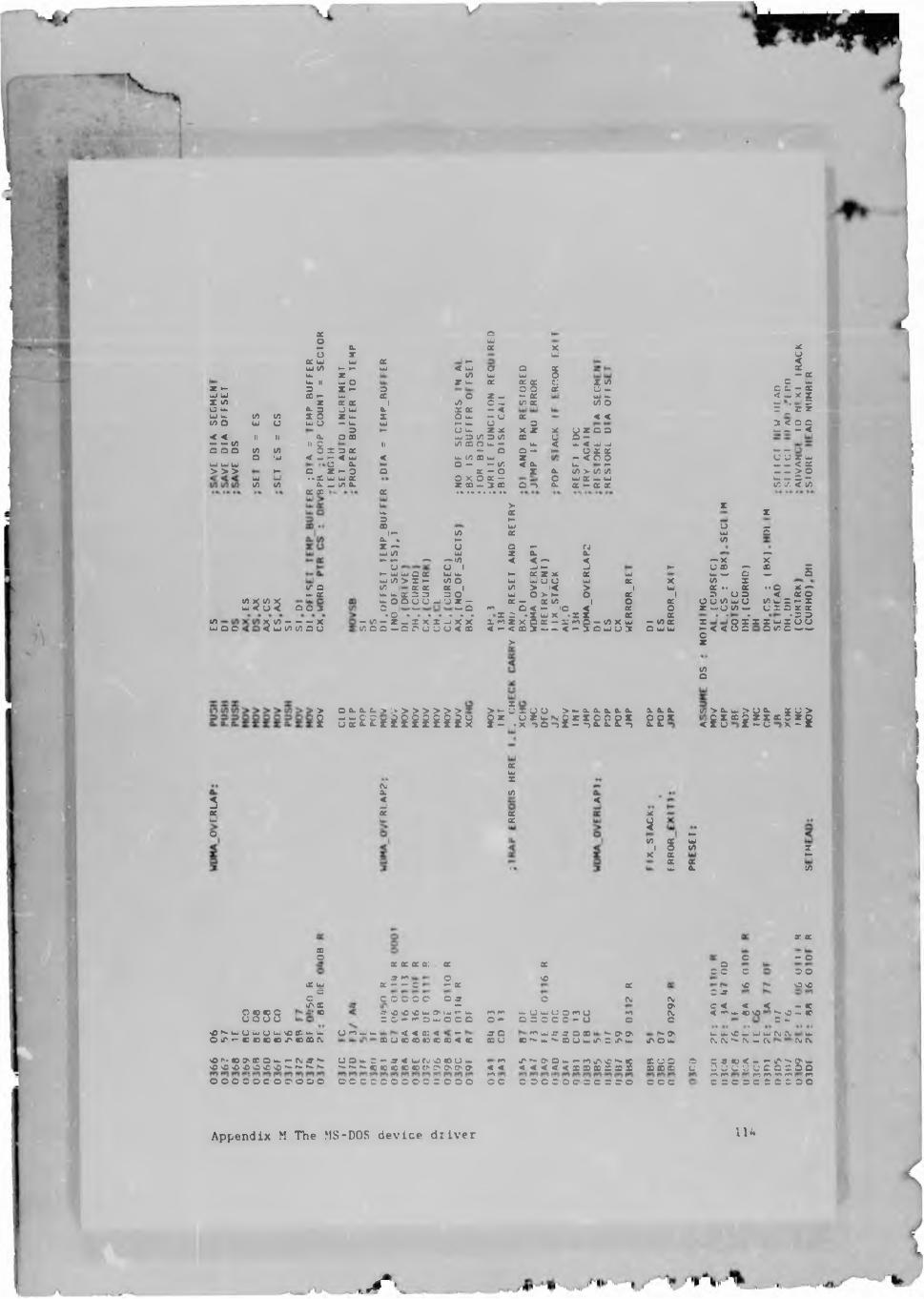
Xow Xo rX w w XW CZ) »— #» wu. zw II w Oz *- D X *- DuJ W cc — — XX to iz X X 1U U. CL D D W XUJ U CZ) (/) X c z w Xc/> O w o w O — w D wft—< < 11 II X O CD— — co II O IIO C O CZ) CZ) c X D Xo w < — F- < W <W W W c x> > > ft— c Z F- O o
w — • • X w w XCZ) CZ) x -j tr xX CD X
25CO uj O O
2332
V* oW. QCOO )
— — — XVO (Z) o u
owcc< Z o oCZ) w wZ ft*- X X XD Oo z w - XftZ) C _J CZ) XX X - <O ft** — U X»— ft- o O W X X X NOw OCZ) DC/) CDCZ) ® O U — u.— o o —w </) 60 w zO — ft— CZ1 < XX - o XO X O X -Z ® ft- 3 Xft* ft* * ft ft* ft* O -5
Xw
Ia:
X!S
CL£
52 5)5 < <
% 5 = =U. < -u u-555u. *—t/> > tZ> V) Uj CC UJ CL — CLX
X
I.c -c a. — cc < - x $?; = l3 < D Ct— u. — <— —223%zz§2tf! X < <A
§!*■' CZ) X * wX oW CZ) w— F- —* *f/)
u u i AND
RETR
Y
LAP1
T)25 h»
XuwCZ)
— XO ® ""ft
z5
i gft- w w O X W ft*. F- CLX X X w w ft— O — aW CZ) > X F- CZ) o W ft- u CJCZ) > l< uj X X CZ) XCZ) X X X I > I w X " X •• o x — ■W. u. x D D D O W O > H O X 1 D O D < at oft*.OOOOWUZ — X — IX CZ) 1 o X © U CZ) w o v> U. = i- XO ' W e— o m O < *- l© < x o Z — U CZ) W u X = X X»© * * * * * * * X D *X W X »X X X X •= 3- C Z ) - Z W Z X Z _ J X X X F O Z X O X - X f o p — CZ) X w — CZ) X e <" < ' § i * X UJX o uCZ)QOw O O O U O < ® <*-<®3Cw^.<«- 3 0 W U 3 O w W O (Z) c ---> i
(Z>O
- > oa.ft.s-> > > > > > > > -!$ d % £ E E i i £ £ i $ i ^
> •- $ O V U > — ft. ft. ft. ft. ft. ft. ft. ft.IE .%%%%|E%2225 ££* v) > ft. u. > u a- x O >< 1 5 * 1 E 5 * f E g
5X—o
2<—XB
xwXto
$<
X
%CO
1 £ *■! £I Xt-
to
CDo
X wc uiAflCr co8 8 8 8
sO^-UJUujUUjsCCC.u-Lv u rr,OtT*- eC<OOOCOJ>«X(\J
x x x a: x^ m ©X •- *“ c #- X
D D C O C C £ZT \0 \0 w O' iw *- u.C©^-f^©UJ©CO
w f * U X < Ci <C •“XUOOCOODODCO< cc
XvOo
r> m u. U uj U © m o O - O O C C C - U^ O w1'u i ^ c O ®CB U 00 CO U uj
XC\JroO
^ C' lT D UT\ ft**I
h» O'kTN O u-
= § co>cc#
c < < << FA ft*. 60 \0U. weJ \0 w UJ Wfv. CL fV •• C\i
or. x— ©D ONO NO• CFft. © W. 00X *•
Pg .X u. X X\OP-eOO'!»Ou.^«i»'~' u o « . c — »<ujrg\e«ou«. 'CO.O'CvOOvO'^'-'-P- •~r«.N.ececaceoeCPC'0'0'0>o o o s o c o o o o o c c c c c c o o s c e o o
M i/'k'0'3w^wjr\£>~or BU S »« < < < < X » X l £ x 5 fflBB V< <mo c C S C C O C C C X X O CCSC a eo < - -u u u u u cI" *> ro m= = = = = =
u"« g> w 0 = 30 ». w. me = = o
Appendix M The MS-DOS device driver 114
. / •
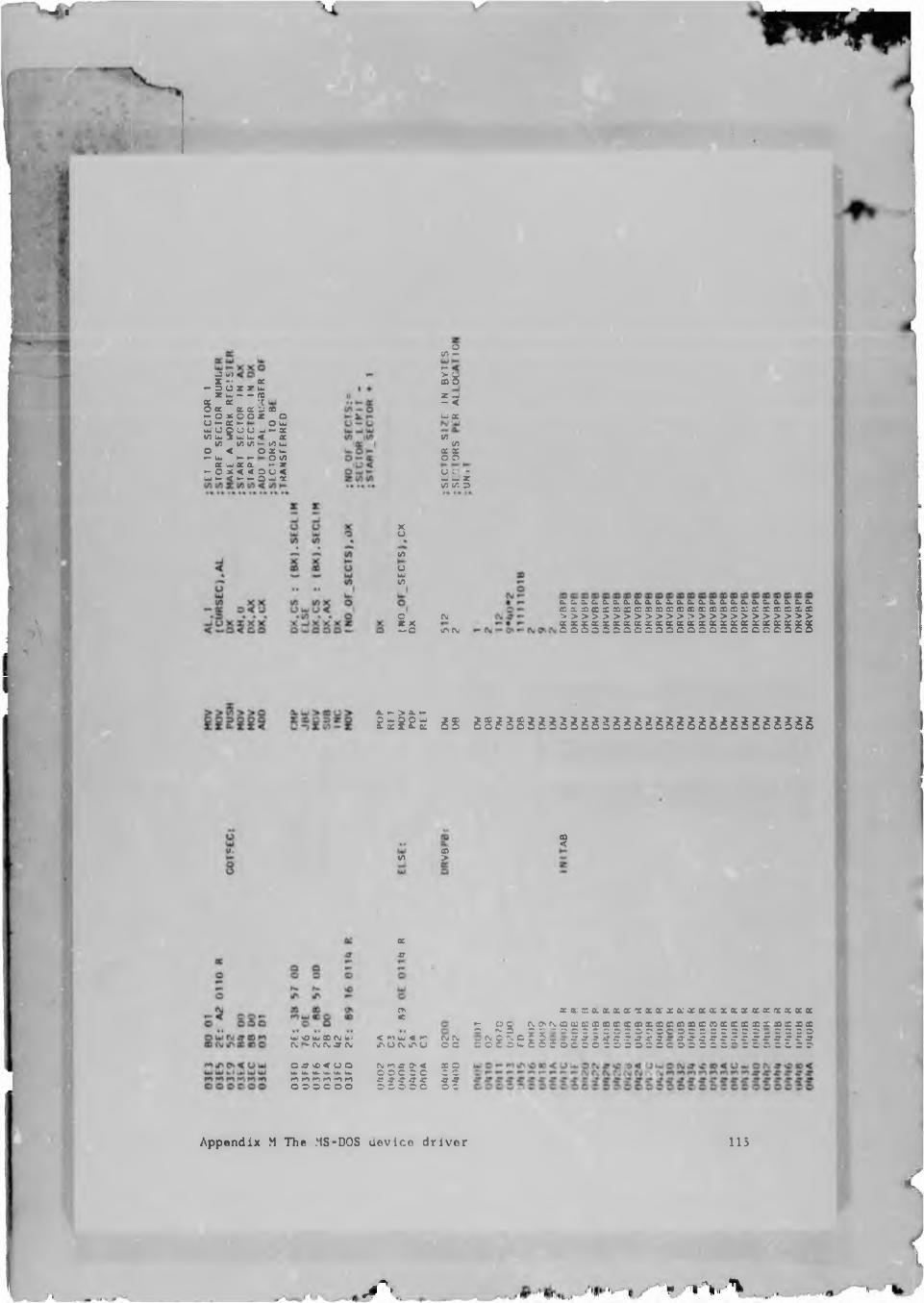
- 4
w: v)X — GC- 3 o z r w2? uj — — ft)g ee etct C. (X L,' 23^ o X o o z o(j _ ac _ o wU-OOUU W f- Z(/) w 3 w w < x(/) l/) (/)— (/) UJ
O < O X U.►— w ►- h* o </)X W X X - z»-OX<<3U< lu«— <*- — QkUX
v-2
i 8z u - <W XV3(/)ggU £. -■--ZV) V. 3
5(/)UwV>
h CVJk/> Ou
6. >- > a. -2 2 i E S
V) 5§
X5T
OnCOUl xc ti, e N Ul < fi w < r- <\i (\J(M {\J fVi J <M XxUfvinu o cOJf v0<OO c\i w a- o- < a ow u. W w M. u. O C C 2 C c Em m m M m m a a a a a a ao o o c o o 0 2 0 2 0 60
Appendix M The MS-DOS device driver 113
XX > ' l r % r %
X X X X X X X X X X X X C . X X X X X X X X X X XXXSffiXXXOCD2DXXCOXXXX23XXXXXX> > > > > > > > > > > > > > > > > > > > > > > >g g g g l g g g i g g g i i g l g g g g g i E i
2 : 2 S 2 2 S 2 2 2 2 2 2 2 2 2 2 2 2 2 2 2 2 2 2 2 2 2 2 2 2 2 2 2
aeaiKa.acKK'xaca.'XKxacKxecxeKXxxa:»- o c M>r\;e(tieirasecemxmKcn83cc»eexexaasx = h-5 r c . T ^ c c r c 3 r o r 3 c a r z = 2 r r r - z = ;o2 g § S £ l i 5 B S 8 l i g g S S S E S § S S S 5 § S S S € S f
<X
X k V '-
oH5</>>
OD CD
I I %
ICL
$
<«c
I ?2 E— UJ(Z) U)
C OIT< 5i o 8 ij
—' —- CM —“<\jX -j X ♦ X ♦2D < X LO 20 —5 ? < « Do. < o. •>. o. o4T X • •^ > C —*C•- o: x x « x - -j>5pcDcax
(A > > > 0.
v><eO
?
1v u; UJ I !§!!§!] ‘“IsSSI O O : .I V u o u o u
' i3 0 i r ' e » r g ' - ' 0 p c u » i ^ 0 ' - 0 r g » w s 0 ,~ ' " & c i
> o o o o 5 5 o 5 o o o o c o o o o o o o o o o c
2
QC CL w CD CD Q
I f Eoo o
I I
"o o
v> i> i23 3
<C
s
U w
a iO 6 iti O fx.»O C c ^ru r~
W#" — JT S ' & X & O
IT OODui^ U n-U ^ u cieoruufloucujo ^^o^ar\j^<oc
>C sc >£)NO sC O VO vC >C© c o o o c e o c o ©
S 2 M S
20cItv>U1I
wcitz
w A
8 (A
X X O C X (-XX u U X W W O W X X W X X X X X © w < < < < a > < < a j Q ) < - - x - < < - < < < < < r f t )® WWWkwjQWW^^) w J>c. Z Z Z Z £ - Z Z E E Z r ® 5 x Z Z X Z Z Z Z 5 L $ 6
— -j-ju-,zuurxuu-Juu-j-ju-ju-iu-.-.z
0)EitZ
• 8 .......................................• OC • • • • • • • e e e e e « e e e w O w •••OCCL &. > — — < —• «j cd - • k oc * • • • u ». « a e. . e = w y a > x
iq x a uj >- a u. x a x :t - — x 5 x _ —• v> -j •Uuju.az z i/) — ix x >• v> </></> i/> x a — o-a£gcia3uxxKxv)v>->>>> -»>>s Q s 5 5 u 5 S 8 S u 8 i i o o 2 2 2 2 2 2 i i
Appendix M The MS-DOS device driver lie
DKVMAX
L
BYTE
H
JZ->
0)
IIh Mr rw w O'c zQ t
Appendix M The MS-DOS device driver 117
■
§ § 5 § o o § § § S S S § S S o o § i § S § o S § iu u o o o u o o u u o u u u u o u u u u u o o o u < in ii iilii iine III
o a x K x x a c x z x x x x U w S x x i t x g : - o x - x ra u x x : < < < < < < < < < < < < 0 < < < < < < < o x < 01 < x y < < :4 ui w ,
X < < < < < < < < < < < < O < < < < < < < y x < y < w X W W W i— « W Lw <0 O ^ Z Z Z Z Z Z Z Z X Z Z Z X Z Z Z X ^ Z Z -----X X X X u - X O W X X X X X X - - X U W - - X X X X< < < < - < x y < < < < < < Q»c<o-y®<<<<
< . z z e 3 Z E z $ E z z E z z z z e z $ £ z z z z z z § E z x f f l 6 £ z z z zu «j u * u -j* u u * u u u u -j u u u u — *-j u u -i u u £ * u h.-j4 z -i —
• e • • w — # M" • X X W I • u •— X ^ ■ w u j X < iC-j O • • r 3 z x • i 1 ■ . — t-
C6 - X 3 3 U w X X X X V) 6)*-</> 0 uj *r><s>— o o O •- «- k/.> x x w o o x x t : x x c x -X V l V i - . Z Z X K X X X X X X - U . .
a. a. . CLIZ> V) < < > X z < <• a a • > • • C X% u — O X X - X X X• X Uw w X z •sV • • X $UJ y % —•v> 1 1 " #- > X c c 3X i X • • » < - X 3 3I < < < ^ — < i> > z CL L. X ,tA ir 1— Q O • i/ i iA a. < w -J H» x x r cl x < < <
a 3 0 1 wj x 5 5 V u ~ — < < X X X < - -3 Z w w O O X X — — w w U X X Z -X X X x * * <L a.X X X GZ l£ a* v) t/> v) (/> v> (/) 1Z> IZ) l/> V) cz>tr - 3 3 3 3
1 I P '> nr N„, ■ft
u u u
— fg <v <*> e » e — i" i— O ia r - r<i M (N, t \ . wo o o o o o
Appendix M The MS-DOS device driver
APPENDIX N THE ENVISAGED FILE SERVER HARDWARE
The hardware required for the file-server of this star-bus network is
described.
The network interface of the file-server should be fully self sufficient
in so far as network management and control is concerned. The file-server
as a whole can be considered as a multiprocessor environment where the
one processor is dedicated to the network while the other(s) is dedicated
to the mass storage system and possibly management of a cache. Communi
cation between the two processors is by means of an input queue and an
output queue which is maintained within the file-server processor's mem
ory area. This memory area must obviously be accessed by both processors.
A semaphore type system for the management of these queues would be re
quired. Requests from the network would be submitted to the input queue
of the file-server along with the appropriate data, if applicable. The
file-server output would likewise be extracted from the output queue by
the network processor
Each ray of the star shaped network requires a single SCC to provide the
1.5 Mbit per second data rate. These SCC's also require the use of DMA
to sustain this data rate. A DMA controller such as the Intel 8237-5 would
be .apable of supporting four SCC's. The memory requirements of the net
work controller are not extensive since the only space really necessary
is a buffer area capable of storing a track of data for each of the SCC's
on the network. This would satisfy the situation where date movement is
taking place simultaneously on all the SCC's at the same time.
The processor power required is not extensive but the Intel 8018b would
be an ideal candidate for this application. A full lo bit date bus is
supported along with all the. features pertaining to the 80188 described
previously. This processor itself could provide a wide bandwidth DMA link
Appendix N The Envisaged File Server Hardware 119
between the network processor memory and the file-server processor memory
area.
Units built along these lines could be included in Multibus type file-
servers or even in P.C.'s with a bus structure similar to the Olivetti
M24 P.O. where it is possible to have a co-processor on the bus.
Appendix N Tne Envisaged File Servei Hardware 120
APPENDIX O EMULATION SOFTWARE
The software used during the testing of the emulator is described. The
listing at the end of the appendix is divided into logical blocks for
description purposes. Most of these blocks do however correspond to pro
cedures in the software, A s t e p by step description is not given since
the principle aspects of the software have already been described and the
listing is itself well commented.
Initialisation of the 80188 The initialisation of the parameters relevant
to the emulation software in this appendix and Appendix P will be dis
cussed in the order in which they appear.: UMCS - UPPER MEMORY CHIP SE
LECT The upper memory chip select line (UCS) of the 80188 is active from
the location specified in the upper memory chip select up to location
FFFFFH. After reset this line defaults to be active over IK below FFFFFH.
Since in this application we have a 8K EPROM which must be selected by
the UCS line this register must be re-programmed. From the table in [4]
if no wait states are required, as in this case, the value for UMCS is
FE36H. I. this case the ready inputs on the CPU are also ignored. This
modifies the 3 least significant bits of the above value. The 3rd least
significant bit is set if the ready inputs are ignored. Hence the value
FE3CH.
Registers such as UMCS form part of a control block that may be relocated
within the 1/0 or memory map of the 80188. In this case the control block
is not relocated from its reset position. The control block starts at
FFOUh in the I/C space. The UMCS register is at offset AOH from the. con
trol block base. Hence UMCSlGC (location ot UMCS) is FFAOH.
In a similar manner to that described above., MPCS is programmed from a
table in [4j. This register is for the mid-memory select lines MCS0-MCS3.
Appendix 0 Emulation Software 121
A 512K block, with an individual select size of 128K, is required. The
ready bits (bits 0 to 3) in this register refer to the peripheral select
lines PCS 4 to PCS6. These bits are programmed as before, no wait states
and ignore external ready inputs. Two additional bits are present MS and
EX which are bits 6 and 7 respectively. MS is used to map the peripheral
in the I/O or memory space. This is given the value 0 which places the
peripherals in the I/O area. EX determines whether there are 7 peripheral
select lines or if address lines Al and A2 are latched on lines PCS5 and
PCSo. EX is made 1 which selects 7 peripheral select lines. MFCS is
therefore 01FCH and is located at offset ARM in the control block, hence
MPCSLOG is FFA8H.
MMCS defines where the mid-memory block defined by MFCS starts as well
as the ready bits for the mid-memory. The peculiarity of the 80188 chip
select logic now rears its head. A 512K block can only start at one of
two locations vis. 00CQ0H or P0000H. This results in the mid-memory block
either overlapping with the memory area that would be catered for by UCS
if it is set at 60000H or with LCS (Lower Chip Select) if it starts at
00000H. In this application it is made to start ,it 0000011 and therefore
LCS is not and cannot in fact be used. For this reason if more than 512K
of memory is used, the chip select lines; have to be generated from UCS
and the upper memory lines. Again no wait states are required and the
ready inputs are ignored. MMCS is therefore 01FCH. This is located at
offset AnH in the control block hence MMCSLOC is FFA6H.
PACS is used to control the peripheral chip select lines (PCSO to PCS6)
Each of these chip selects is active for one of the seven contiguous
blocks of 128 bytes above a programmable base address. The only re
strictions on the choice of base iddxess is that it must be a multiple
of IK i.e. the lowest 10 bits are all 0. If the control block is in the
I/O area then the addressee activated by the PCS lines must not. coincide
with the location of the control block. A start location of 0800H was
Appendix 0 Emulation Software 122
chosen. Two wait states are required for the Z8530 SCC's [9] hut again
the ready inputs are ignored. 1’ACS has a value of 083EH. for the above
mentioned conditions. This register is located rt offset A4H in the con
trol block hence PACSI.OC is FFA4H.
The dynamic HAM devices require that each row of the chips be. refreshed
every 4 mS. There are 256 rows. If we use a method where the time between
refresh cycles is constant. we require that a refresh cycle be performed
every 15.625vs. (<tmS/256). Timer 2 of the 80188 is programmed to request
a DMA cycle from DMA channel 0 to satisfy this requirement.
Firstly programming the timer:-
Timer 2 was chosen to perform this task since event hough its capabilities
are less than the other two, it does have what is required. It is also
the only timer with an internal DMA request. Two registers need to be
programmed viz. the maximum count value and the mode/control word.
The maximum count value required to give the necessary DMA request spacing
is calculated as follows. The system clock frequency is 6MHz therefore
the maximum clock input frequency is 2 MHz. (Hardware cha"..cteristic)(4)
Therefore T = 500ns. The count value is thus 15.625us/500nS = 31.25. A
count value of 31 will give a 15. 5vs gap between refresh cycles which i s
acceptable. Hence T2MAXCNT is 31. This is loaded into location T2CNTAL0C.
The control word is set up so that the counter counts continuously, and
interrupts from this counter are disabled. A number of other parameters
are fixed as shown in |4). This gives T2C0NTV a value of C001H.
Programming DMA channel 0 will be discussed here eventhough the variables
are only listed later. The DMA channel is programmed to perform memory
to memory transfers. The source of these transfers is set initially at
the base of the memory 00000H and is continuously incremented over the
full 1Mbyte range. Phis lias the required effect since the row addresses
of the RAM chips are multiplexed from iddress lines AO to A9 and thus
Appendix 0 Emulation Software 123

these chanye with each DMA cycle. All 256 rows are thus cycled through.
The corresponding column addresses that may be generated are of no rele
vance. The destination address is fixed at a location in the EPROM range
and hence the writes to this location have no effect. The terminal count
is set to 65535. This gives the following values for the variables DMAOTC
= 65535, DMAODPU (upper four bits of the destination address) = FFFFH,
DMAODP = OFFFFH, DMAOSP = OOOOH, DMAOSPU = 0000H. The suffixes SP and DP
refer to source pointer and destination pointer respectively. The control
wor-1 for the DMA channel is set up according to these criteria: The des
tination address is in the memory area and must not be incremented or
decremented, the source address is in the memory area and must be incre
mented, DMA activity must continue after the terminal count value has been
reached, no interrupt must be generated when the terminal count value is
reached, the transfers are source synchronised (SYN), select highest
priority (P), DMA requests from timer 2 are enabled (TDRQ), and DMA ac
tivity must start immediately (ST/STOP).
|" |T QIC j MC "'DO' MC : WC TV err m P |td*o » i*11ITS# l,w
oemNAnoNCKO/RBCWJ
The first action taken after reset is to set the UCS line to FE000H and
then a jump is made to this location whore the remainder of the
initialisation cakes place.
The Memory Test The memory test does the following: The offset of each
word is written into each word throughout the entire segment. The contents
of each word, starting at the beginning of the segment, is compared with
the offset of that word in the segment. These values should correspond.
If they do not then the memory location at which the first mismatch occurs
is faulty. A similar test is then performed except in this case the com
pliment of the address is written in each case. Again after the whole
Appendix 0 Emulation Software 124
these change with each DMA cycle. All 256 rows are thus cycled through.
The corresponding column addresses that may be generated are of no rele
vance. The destination address is fixed at e location in the EPROM range
and hence the writes to this location have no effect. The terminal count
is set to 65535. This gives the following values for the variables DMAOTC
= 65535, DMAODPV (upper four bits of the destination address) = FFFFH,
DMAODP = OFFFFH, DMAOSP = 0000H, DMAOSPU = 0000H. The suffixes SP and DP
rofet to source pointer and destination pointer respectively. The control
word for the DMA channel is set up according to these criteria: The des
tination address is in the memory area and must not be incremented or
decremented, the source address is in the memory area and must be incre
mented, DMA activity must continue after the terminal count value has been
reached, no interrupt must be generated when the terminal count value is
reached, the transfers are source synchronised (SYN), select highest
priority (P), DMA requests from timer 2 are enabled (TDRQ), and DMA ac
tivity must start immediately (ST/STOP).
11"'raj owe i wc "'DO; | "C TC NT m p rowo * f
mr*! •w
ocmNAT.nN woeno
The first action taken after reset is to set the UCS line to FE000H and
then a jump is made to this location where the remainder of the
initialisation takes place.
The Memory Test The memory test does the following: The offset of each
word is written into each word throughout the entire segment. The contents
of each word, starting at the beginning of the segment, is compared with
the offset of that word in the segment. These values should correspond.
If they do not then the memory location at which the first mismatch occurs
is faulty. A similar test is then performed except in this case the com
pliment of the address is written in each case. Again after rhe whole
Appendix 0 Emulation Software 124
segment has been written to, the contents are read and compared with the
complimented offset. Again if a mismatch is found this memory location
is faulty. In this way each bit in the whole segment is checked to see
if it can be set and reset.
The code to, do this test is shown in PROCedure TESTRAM in the assembler
listing at the end of this appendix. The unusual exit from the procedure
is necessary because the first time the routine is used, a jump has to
be made to the routine instead of a call. There is nowhere to put the
return address for a call instruction because the stack cmi only be set
up after the memory is checked. The routine is therefore 'jumped' to check
the top most 64K segment. If this memory is functioning the stack is set
up at the upper end of this segment. All subsequent memory checks are
made using a call to the routine. Each phase of the memory check is in
dicated on the diagnostic L.E.D.'s.
ini tial isat ion and programming of the Z8530 5CC ( Emulator SCC ) The
method of programming of this device and the initialisation required tor
the emulation software is described. This is done in the Z8530B_INIT
procedure.
If we consider only one channel of the SCC on the hardware level we find
that only two I/O locations are used. The SCC however has nine read reg
isters and sixteen write registers. Some oi these registers are shared
by both channels [10]. Read register 0 and write register 0 can be ac
cessed directly by the hardware by addressing the control register of that
channel. Write register 0 has its four least significant bits that can
be programmed as a 'vector' to a required register. If one wants to write
to register 10 for example a write is first made to write register 0 to
set up the 'vector' to register 10. A write is again made to the same
1/0 location with the data required for register 10. The 'vector' is then
reset back to 0 after this write. Similarly a read from a register other
than read register 0 requires a write to register 0 to set up the vector
Appendix 0 Emulation Software 125
followed by a read from register 0. The transmitter buffer (Write register
8) and receiver buffer (Read register 8) are exceptions to this rule and
can be accessed directly by addressing the data register of the appro
priate channel on the hardware level.
The SCC is programmed to function as a Bi - sync receiver / transmitter
using NRZ coding. It obtains both its transmitter and receiver clocks from
external sources. The Bi - sync mode was chosen so that two
synchronisation characters could be specified and also since the bit-
stuffing used in SDLe/HDLC communications is not desired.
The programming of the individual registers will be discussed along with
the programming method.
The procedure called WR was written to perform the dual writes required
for most of the registers as described above. This routine requires that
the DX register of the CPU contain the address of the port to be written
to, the AH register contain the required SCC register to be written to
and AL contain the value to be written to the SCC.
The equates used in the assembler are the following:
Z8530BC - Control register of channel £ of the emulator SCC.
Z853UBD - Data register of channel B of the emulator SCC.
Z8530BDREV - Data register of channel B of the emulator SCC but with the
data bits reversed.
Because, of the dual write programming described above it is possible that
when one starts programming the SCC the 'vector1 in register 0 is set
pointing to some other register. Before the device can be programmed
therefore it should be brought into a known state. (In this application
this could he regarded as a redundant step since he SCC is reset on power
up). By performing a write to register 0 requesting register 0 and then
a read from register 0 we can be sure the pointer is set back to zero.
If the case where the vectoi is zero initially is considered, by ro-
Appendix 0 Emulation Software 126
questing register zero ue liave left the vector unchanged and the read will
be from register 0. If the vector has some other value in it then the
writing of a zero will put a zero in which ever register the vector was
pointing to and reset the vector to 0,
The channel is reset and then configured.
The configuration selected is: x 1 clock mode, 16 bit synchronisation
character, synchronous communications mode enabled, no parity.
The clock sources are: No XTAI. i e. the internal oscillator of the SCC
is not used, the receiver clock is input on the KTxC pin (from the MFM
decoder), the transmitter clock is input on the TRxC pin (from the MFM
encoder).
Register 10 has various control bits that are programmed as follows: The
CRC generator and checker are preset to all ones, NRZ coding is to be
used, a full le bit synchronisation character is required.
The control bits in register 14 are programmed to disable the Digital
Phase Locked Loop in the SCC. All the interrupt enable bits in registers
1 and IS are all disabled.
The initial synchronisation characters programmed are 4EH bytes corre
sponding to the contents of the gap 1. See Figure PI. Note that the bits
of these characters are reversed since when they axe written to the SCC
they are not reversed by the hardware.
Finally the receiver error hits are reset. The transmitter and receiver
th vnselvos are nut enabled until the track emulation routine is called.
The actual CRC polynomial required is chosen by one of the bits that is
in the s a m e register as the transmitter enable bit. The required CRC is
that used in SDLC communication* viz. x 1* + x 11 4 x' + 1 and is selected
by resetting bit 2 of register S.
A brief description of each of the remaining routines.
VEC.TBL.INIT Event hough interrupts ire not used in the software the
interrupt vector table is initialised to a known state. Each of the vec
Appendix 0 Emulation Software 127
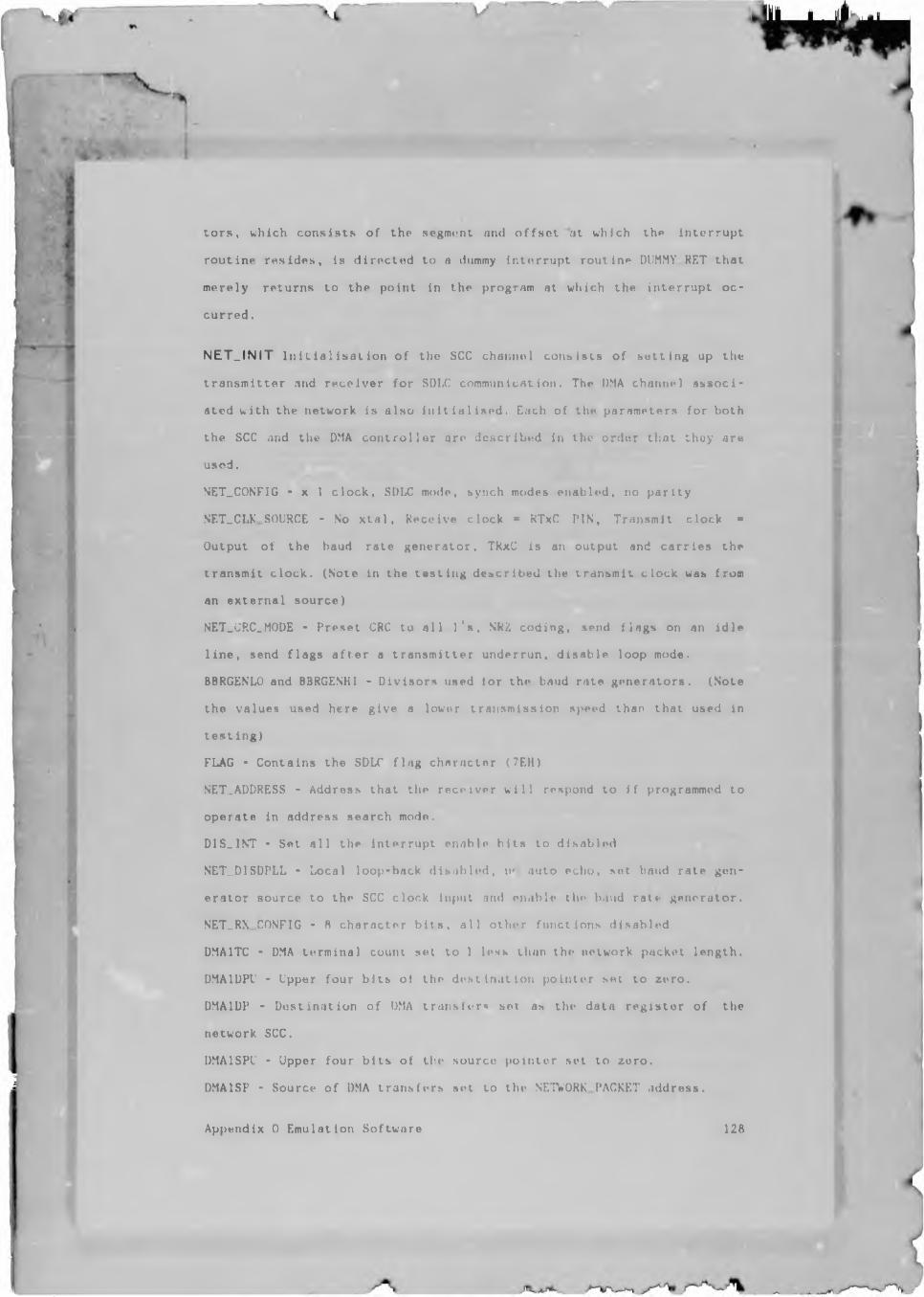
tors, which consists of the segment and offset at which the interrupt
routine resides, is directed to a dummy interrupt routine DUMMY RET that
merely returns to the point in the program at which the interrupt oc
curred .
NET_INIT Initialisation of the SCC channel consists of setting up the
transmitter and receiver for SDLC communication. The DMA channel associ
ated with the network is also initialised. Each of the parameters for both
the SCC and the DMA controller are described in the order that they are
used.
NET_CONFIG - x 1 clock, SDLC mode, synch modes enabled, no parity
NET.CLK SOURCE - No xta1, Receive clock = KTxC PIN, Transmit clock *
Output of the baud rate generator. TRxC is an output and carries the
transmit clock. (Note in the testing described the transmit clock was from
an external source)
NET_CRC_MODE - Preset CRC to all 11s , NRZ coding, send flags on an idle
line, send flags after a transmitter underrun, disable loop mode.
BBRGENLO and BBRGENHI - Divisors used for the baud rate generators. (Note
the values used here give a lower transmission speed than that used in
testing)
FLAG - Contains the SDLC flag character (7EH)
NET_ADDRESS - Address that the receiver will respond to if programmed to
operate in address search mode.
DIS_INT - Set all the interrupt enable hits to disabled NET_D1SDPLL - Local loop-hack disabled, iv auto echo, set baud rate gen
erator source to the SCC clock input and enable t h e baud rate generator.
NET_RX CONFIG - ft character bits, all other functions disabled
DMA1TC - DMA terminal count set to 1 less than the network packet length.
DMA1DPU - Upper four bits of the destination pointer set to zero.
DMA 1 DP - Destination of DMA transfers set as the data register of the
network SCC.
DMA1SPU - Upper four bits of the source pointer set to zero.
DMA1SP - Source of DMA transfers set to the NETWORK PACKET address.
Appendix 0 Emulation Software 128
NETDMA1CW - The control word is set up as follows - Destination in I/O
map and address to remain unchanged, source in memory area and must be
incremented after each transfer, DMA activity to cease after terminal
count reached, no interrupt on terminal count, destination
synchronisation (SYN), low priority channel (P), disable timer 2 DMA re
quest (TDRQ), start immediately (ST/STOP).
is"'raj D«c i me M ( Oj oec I inc TC INT T 1 ’ two! x I t
oetnNATKw •ounce Moewa J
NET_TX_C0NFI3 - 8 bits per character, all other functions disabled.
NET_SEND This routine generates data for the test network packet and
initiates its transmission from the SCO. The information included in the
packet includes the address of the node tc which the packet is being sent
as well as the current variables from the emulator. The first data byte
is loaded into the transmitter before resetting the EUM latch for the CRC
transmission at the end of the packet. The DMA request function for the
transmitter is also enabled.
"TRACK _LIST_INIT The track cache index h o be initialised before use.
In this case the 42 available data block ^re assigned to the two sides
of the first 21 tracks of the disk. The drive number and application
number are. initialised to values that would not normally exist during the
emulation process. The various records making up the index are initialised
as well as. the pointers to the respective data areas.
TRACKO.IN IT This routine initialises track 0 on the emulator to the
state that the corresponding track on a physical disk would be. in imme
diately after formatting. Procedures FIRST, SECOND and SIXTH are used to
initialise individual secton; to their required states. FIRST is used to
fill the bootstrap sector (sector 1) and the second sectors of each of
the File Allocation Tables with zeros i.e. sectors 3 and 5. SECOND gen-
Appendix 0 Emulation Software 129
crates the first sectors of each of the File Allocation Tables. SIXTH
generates the contents of each of the sectors occupied by the directory.
S C A N _ TR A C K _L IS T This routine returns a status whether a particular
track that is required has been found or not. If the search is successful
a pointer to the data area required in the variable TRACK_SEG. Parameters
passed to the routine include the required drive, application number,
track number and side number.
Note that in the assembler listing that follows a number of brackets that
would normally be square have been replaced by round brackets for
typographical reasons.
Appendix 0 Emulation Software 130
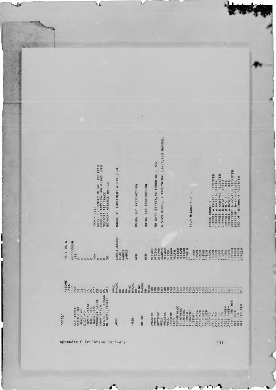
Xk
Q O w w X— (/) Z< 3 3U )
ZUJ — <Ul zo x w zZ u. < o— Z u.W o 3 KCD ~ X X z o— O 3> < < UJ z z-J O Z O UJ
t/)z - to X zuj a. z to X•— Z Cl uj l*.
<0 Z < CL x O- 3 O \-J o — to X H-z z z
x UJ u, C p o SOo > z — 5 z 00< — Z QJ r-Z Z =3 UJ UJ oh- Cl U tO Z oo
a:
sooo
$
i °
a
§ocu c — 5ou>ooooo«roooou
(\J
— Ou
* o «y S
><wQCO
<rQ.
oo
<
5
c.Q.
t/)wX
_J
2wXCL
ccUJar~.
%
xOJ
<
tnacu,)Q:<<^2:-< < k — —o o tn o
V)012
1o
inin
o — o —w tC w (/) c: — cr —
o c— — Uuc o: o c: o: K— < — <
K Z - Z -u . o < O < — u o u o< < CO CO-J__1 -iW W W W
i l l i = = = =u u u o
O 3 O O K— u-' s: —t/) V) — 22 — <r s: z a. lu c X D> > U (T K -J U. < Zz x c r -co < *- — z 0. £. —— - r =>w W z Zz z z z o3 Z — —< < — — Q
(J O — — uJ
%
X S X X X X x x x x x = x xcoecti\cx^xvot\.o>- x x x x x r r r r . = = = ocec.-\-ju. ui u. o u. u. u. « u. w o o e o e o o o e o o c e c c o c o i - — — i- u-u-^-uu. — u-ecu-u-u-U — - c o c o — c r c r c c — — - — O O O O O O O O C O O O ' ^ O O O O O O O C X O O O O O O O C O C C ' O O O O O o o o
-
8 5w — u i/) </) v>
! g 2 § 3 § s § 2 3 § § 2 2 §XO H .
UJ < UJ H- > Z XUJ — ►- u</) «- Z Z I <
UJ O ^ O in O -J z a . -j z o u. — i a. w i CC i Z OOl / } — *- CLO.Xt < a ix i i i* < iocCO -Ox IX x x IV) o<6 ih-ULuuuuaca:--!o uo<o<<<xa:Uf-
oo luwo: — a s x x o u j u jt >i/) — v) — — — oui/iz
Appendix 0 Emulation Software
c 21 U ='= = = 2= = = = = = = = = = = = = = = = = = = = = = = = o?:$ s 2 3 s : 2 5 x 5 £ x 000'c!,0::,0,0,{7oc?® o a c y o o a o a 5 5 5r'5'555o
X $X CO h-z z o-5 o
8 8mm' rnjto a ) c/3
5^° 88 8 2
( /) CO
1 1
10 V)
is<J) c
CL ►-y orvj ru
> ><- u o uo^Z-NNNNI\C = L: = = =.=-UQ:<<x:~2-<<srx< _ z x o o o o = % = : = z = =
C I >- ITV 1X> iA S. J' ^ —cvevooooDcoeosocrefsiiCKX ► -► -O NNN rsi — Si'sN N jN iiS i —
131
oat
y - O§ 2 =
<
.
> >
IIzi
V)(X
55> >■
8U E 5
255 5§ 5g :(/) O u. <
2 §
1C1 1> > (/) (/):o xX »- (X g< i— % — #— V)
S3 <53 CO O sO %X X
5 5< U. X <X Z < II X: S 3 n - - x
oX X X
d d "cXXX l i
ruuxui^v^h*. I/) X — Z X U. »X Z X X J) X x X
O u tnu. UJ UJX X X Qu:(/3wi-XX X < % ® oo 2 <
— u u > cISxi^SEuJ X «— w — w U w - Ui - X > XX-Je-w X»*U —< X ww — Lw *W— < (Z, u1; x n u-XXU.U.ZLJXUI CU.WJXX — xzx
= 35 5■*. < u. 25 (/)X 1C X X
i l i i
l i ? =»- LU CZ> (/)
x x x x x r X XC O O O O O C O
i o S S o S o B g B B S S s g s S o S o g B S S B o g B S g s s s B B g B B s B B B s s S B B B s i B B B g i g g
u uS34 - = B^ =Ui
3- X X u c u«<= £- U' Z u. > | v. - v r = -• v s z z z a: — z o ac tr a. — r z o s. - c zU. 3 -J X C <-3<U. = - . U < - « —r w. 3 V) i u u. * y. 3- = - 3 3 z ie e < — z z r - w. 3 v; $ u. u. a. y 3 v — zz c 3 z z y y w z < - i w w u <- u - — iz vi r — - c x x x y 5 x x ------- .- z - - a- is; - z z - - -x u 3 x r 5 u 3 « - — - 3 3S— rvmsry'S’ aua — --- — — — 3 X X w o u 3 — 3 3 3 3 u 3 Z 30 0 e u c u 3 0 0 0 U 3 0 y u v ) z * 3 3 ---- 3 < y y c T 3 - i3tn«- iy y z 3 u < 3 z z - - - < ---- 3 -----
w w w ^ « u u w w ^ . w J » u . w * . — C C X X U U X X wJ — X — *— X X u . » > X X X - > wn — —. — w w w X * — *»X U U X X X X < X C X X O X X - O X u J X X X U Qx x x x x x x x x x x x x x x x1 I
•*. ** ^ h*« — » 1* — — * • •— •* ■>•u-XO*- C/3Z. X X Z » r 2 Z < X X Z
Appendix 0 Emulation Software 13:
v .*i <• .
1/
> >X X< < ^ zU. Zt — —a. clC Oz z ou
x X‘ * X Xz z — —— idJ
x .X55 %%
ITc:
s
-cO
o < cc < - a: a: < w :<C3 : = z : u e: d o) O u. <t«J V10 (0 CD < c.z z z X X Xz Z uJ c uJ X WX c- a. X 00 < X to <X 3 < r z
05 Z Z fv. U U 3 X t - X to to<> • X X mJ X < 3 < - X X Xa. (/) (/) {A X z < # X8 X x z s CD < X X o XX II n < < < 1 z 3 X w X X</) X X X o — s r u c o oX Ui 50 CD W -Jw O K Z C U < L)to to < u.U U w u to X Z X UJ - 3 toZ ■0 r X f f i z z a. x X X u u > 0 X 3 X to X XC/5 x cr z < < o wJ X X Z X $ to X X x UJ < << X X c u X X 25 Ly t/5 U UUJ X u 5«JX X < < 3 u -j to10 X > X u.
ac £ m X OU X X X u — toc X< U o X X W wJ < X Urf < u, S L. u- zV5 C O X w L3 (/)(/></) CDCO < to </> < to to to NJ < zu u.1 O p w w w z to z u . Z UJ X UJ X > >O X x a: x z z c or x x x o ooC O w < O u j ^ u X X X z X — UJ toto
i
z - j i t c ^ z -C - V c X U w sv: a. - r s c ^ - c rz =" Z coo:L3 u x c — o < u. - — 2 v; r uj u.
Appendix 0 Emulation Software 13:
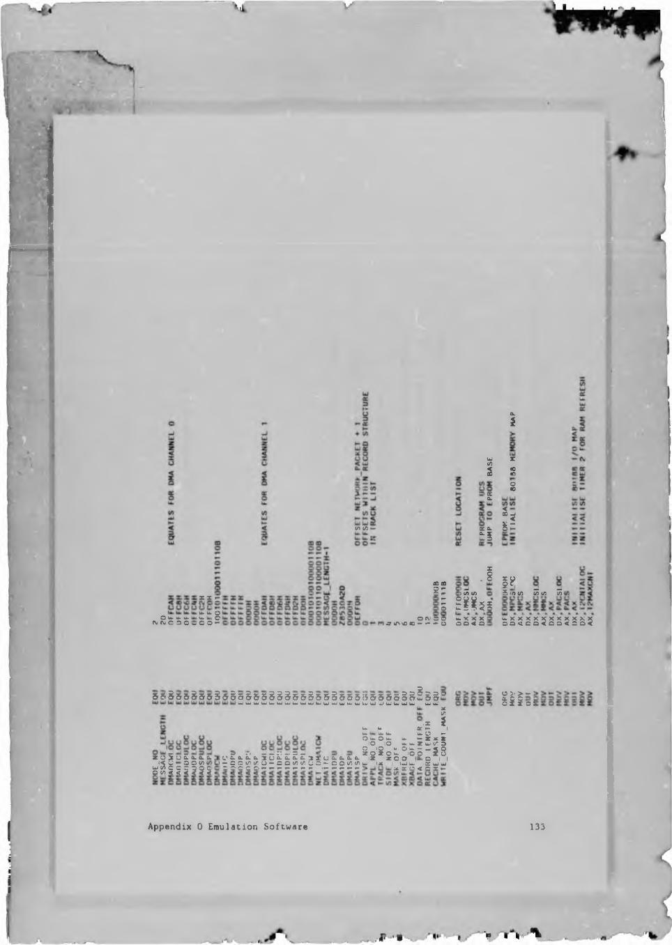
l/> I/) —
ZZ %u- u. Ou- C OO-O u. u. u.(Nj Cg C O O w
a.
5
UJcn Z5 0000
Eg
El is® »g:
XJ) u> t/> CA
i E i l s s
I?5<aia — —</></) V)
OCX' 5 O ^kA'aoO— '——"O u. X X X < O O < o: 5 5 5 5 5 5 5 5 5 3 5 $
xu^uCaiau■ l i s i i l ?
5 5 § 5 & g 5 5 § 5 S 5 g 5 5 i § § 5 5 § 5 5 S 5 5 5 i 5 5 5 5 5 § g £ & §§5 = 0W WWWW W W W W w L J W W W W W L w W wJWWWW uJ u-Xin
o >* > — :glio!
■0 «T < — ■■ D w« 3 *i (.' 6. a o. a % u a a a a % ± u <) — ccvotA/U— comiruo — ocmmu. ix iu uj ;o: w w x ac c < o z ►-i a a a a
iz iU u Of t - Iu. u- u, u.' O *-ra — o u. u. —x x xIO IO — W X ui v: 3O lO lU- O u. — _ <
X O X O U. _IO O |ix ixoo _' O O C C O — — — — — — ^ '— — — — —
■:3S. O II
Appendix 0 Emulation Software 133
,JP '• > » » %
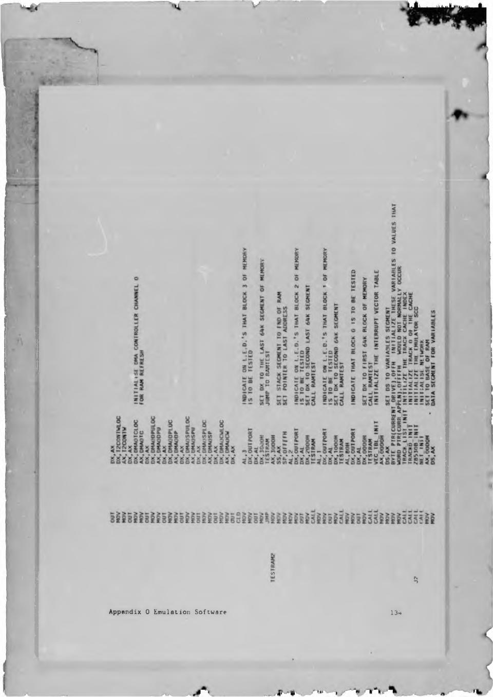
l/lCM-)
Appendix 0 Emulation Software 134
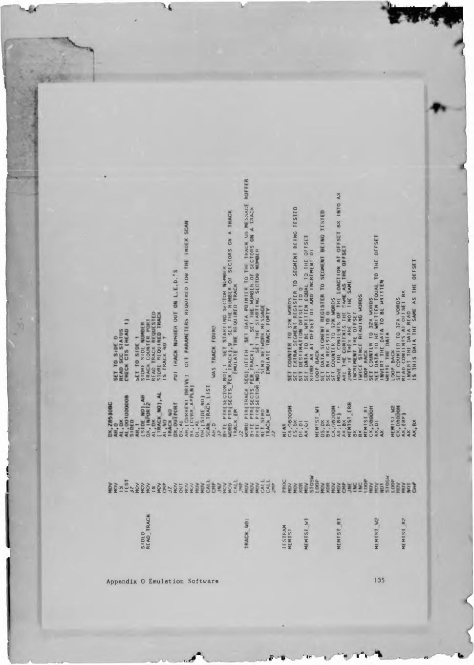
u V
O X
CZ)6
8QC
1
m xU) u a: a: uUJ X w 2S s S S -^ % W M. to</) »» 06 c/5 -
i
8u.051u.06V)
i 8
I ;
- a. z <
</>
«« X -*<- -J (— o < — < <
g j
_» e l— - U — V5 I<«— «.»< w * oH i s i z i
1 1
<8in8Hoa. wuJ t/)
h 306 O8S2u s _w Z O </> w
5 f lCj ^ W Z Z WK3 < </>
</i x —
, ni f8 JUO w wC/> </5z xXx x _ at W O O
CZ)$
<N. > <
o
II
e a ;
% 3 «Z O w U Z
i 35 * o o 8X Uz w w
w ffi (Z)
| h
< - < to z►- *- co O< — y> lu u.O w xlf> W X #- X X o^ w.►-X —»(/) w wxx Z XW U < w < O w oz - z 2 •X .u Xx» i—»co w
CZ) X |ZV,'S< uuZ w w- to IZ)Z Z Z O XX ^ x wX X X w |
CZ) XO w X IQ: x <) > > w z ru
owCZ)wXg WMX COflO XX —*oozX XXX X z3 x XX Xto o xX zo oX X zo < -zw O ao
CO x w Zo co <zp O x x —5 x cz) x o
tz>w
5o
$
IZ)
:S£ 5 SiCZ)o
CZ)xxowXxO
Z X x
CZ) w C X
{\i — O Z UJ •- (\j (/)m z 3t V> h- m«-
O uj u.- «e o5 2 ;
z$wCZ)
5 S < 3W Q Q W — — OW W W XCZ) CZ) CZ) CZ)
•- M V)
5wCZ)Xfl
8 CX CZ)
rz _< x O w |W H #"2 - 8O w UW X cZ Z wx S 5CD U Wx x >wx Ocz> cz) f
- I
58CZV M X X X5 g SCZ) X Xx Z O z <X wx > X Z x x O X
X - XX Xill
5 :CZ) O —o cz) w z0 Z Z 36% O w w5 x 0Z X - O1X o x X <Z X o < xX Z O ° Ou X X X Z at X xx
o O < XX u O Z XU — w »-
X XCZ)CZ) — 5
CZ)XxO$$ HCZ) CZ)Ox <
p CZ) X§ : S 3Z O X CZ) fv Z r-> — x
o 5 5- 2 5 < - - <- — — — < - - - X o
l i r -S 8 ° S Ea. O x x8 X Z CZ) x CZ) Z — —
)Z(ML ___Ex-jiOZZx-j
8 J ox J- 8 8 5 3 2 8 8 8 5 8 2% » • % X * • • * • X
£ 58COO-j oo
X c Xco o m— o 5i8253 $28553=^885553 $5535
• > <« > > > >- >•->>: ! i 5 2 S g 8 g E i 8 5 5 $ 8 $ $ i
ih '— Xto z
; m 5 i• -J u z• 3 3 8
8 > > V) a 31-
*5 xz to 3COX zX XX x z
to5XZtoX$
MztoXX
Appendix 0 Emulation Software 135
/ f / #- > ' Tl H ■ /!)
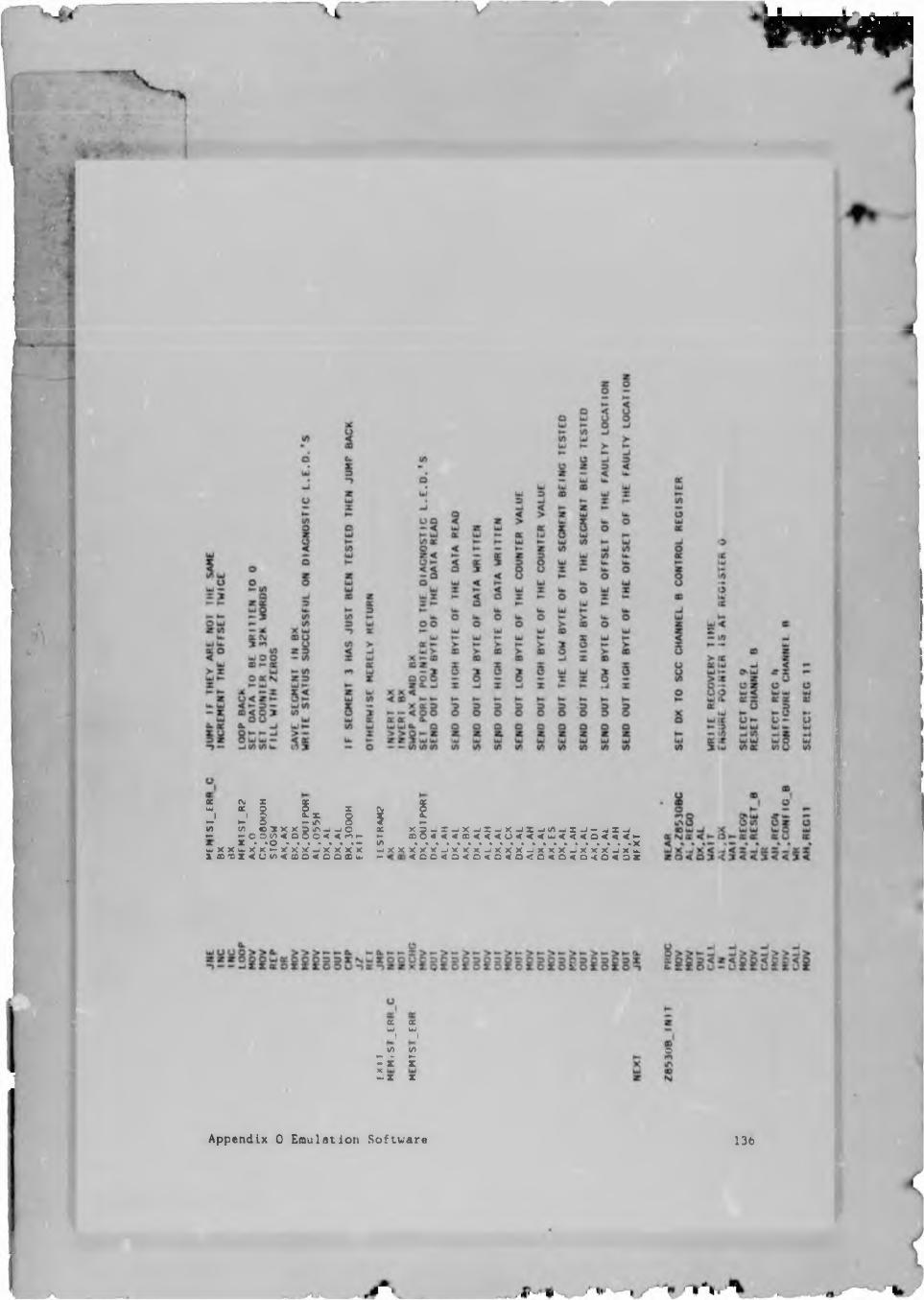
5 5 1 h i i Iv> vi b ■* >< x 5 ir-j-j o oc x = _ s-j x j s j x-j z-j v) _j r _j - -j x-j» ~ 0 3 V ) < 0 0 0 < < m i - *- ® 5 < < < ffl < < < U < < < uj < < < O < < < ►-* Z • %0 * * * * * * * " t/) * * * * * * * * * * * * * * * * * * * * * xW X X w X X " - X X X - ; X X X X u j x x x x x - i x x x u x x x - i x x x - x x x - j x u : l B « X 4 U e z > < X O « O O C D u J — < 0 0 < 3 < 0 < 0 < 0 < 0 < 0 < 0 < 0 < o x
« eew wI IV> V)<“ • *-- X X
1 X X
r w f l p
o
Appendix 0 Emulation Software 13b
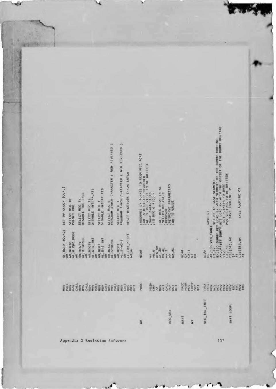
Al.B
CLH,
SOUR
CE
SET
UF CLOCK
SOUR
CE
a.•a c
V)Q.3%lT> rc
<LD5
</)q:>UJx
IO
Xw>wor
xw
I
£ 503wOC
Uuj w V> -J wK £
uu — W (/)
ww o os u co u e ooc u <(/> w < UJ < Uf < UJ O W Vuj —J </> — u5 -j V) u O —j (w — cn o I - UJ X(/) O (/> x
OC a- a Lf> —o u o S o v)u. —
bc aUJ I UJ —x to x a
! $ £ $ $ < 5 5 £
— Ic tnX
3 *£ vi
5
i$
W W >0 U ^ U >o >• o >w V)
X
w X
oUJX
V)
Ia xUJ iux h
l o ix w X wo — m
^ BoC/> 'uJ H.u- XX UJ tz> >- X 3 X2u. w — O►- < - a1/5 > uj UJ X - X X1 O UJ <Q
IZ) XLJ £ < °
V) x X
UJ(/>(A wX Xg 1
o r Xw v X -JX (/) UJ <
<x -j e6 U X< < !l « 3 X
x O X </> t/5 uj 3 — — w Xu> >
c/>U X< wX X— w
g -w o
X U > UJ UJ UJ o X ►-
§ £ £ £ § • * •» •• • •
5 5 £ £ S l 5 §
5 u . ° =w X uj U X
VIU j O ffi UU —t/5 Ui X &J
or o w wW — U- o X z
^ X 31 H -< u. X u.= 5 3 = 2 8 82 x = E 2 e
X
i f ) e « o u uj wO 1/1 O U L- > O Q -J > < 3w < — V) </5
5^ O f- UJ lAU- -1 UJ </> lA V) X (M
5 $
5 1£ 5 5 5 5
I* ™ O O u. i/\ —UJ X UJ » lA V)cc (a o /iooai —
U V):e o x v ) x x - x v ' - - < a -<aeD«vioov)v)ov)
!58i5! M !5! i s i i s ! ;H l 8 £ £■j' U. U tt. u- ►. _ V5 > o x U.
85£8£ £2822£ 8 5 :£ 8 1 H i
Appendix 0 Emulation Software 137
. /•.. * » '"" . > .
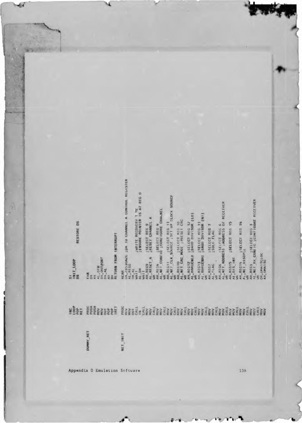
w
M X
X% O —O OO 06*- CL - ODO o *-
W H» UJ W06 u j a: cACA w••o u ?UJ w U# #*-JO - J
u i 06 U I wCA g CA O
(V m
QCH>wouJ06
to O P"
a>u,Uu.(L
w — Lw — W Oec > k > a <o
oc > o
w Otilv) m I o
o«L. ■K >
5=V) 03
ocaU . V ) 06 W
oUJa:
u tUj «ow o - •*u j O wCZ) (A CA V)• CA
5 8 << X X -J* * x‘ Q < < O O XXU,
A Se w -j M K 4 >z 3 « c :
•“ u op _3 1 I I O •- O O I I I #- O — o 006 006 O < O ’- OCA O — C —w w UJ uj uj uj uj 60 u* (£ u. u w w u- — u. W UJ wwIo *W CC06 ec5V
T ll
Cu.06#—-<z a K 8
^ oGJ
o-w u.
:: w- OV ) Z
Xx
K u X * K Q§ 5 ^ $ $ ^ $ 5 < 5 5 3 $
L
a
5 < $ § 5*
Appendix 0 Emulation Software 138
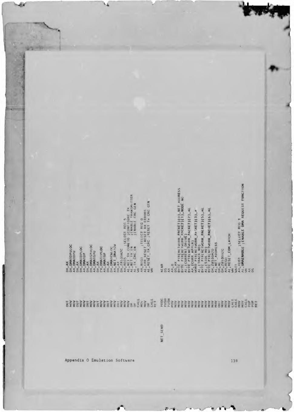
> 4 ' V
8 y 8■■J 5 uO 3 u 3 3X X X X a a.o o o o V) w A.m
06§■►» z- r ...
x $ 3o
* (0 u< o 1 1W% 06 c o% - u Xass 0 06 XO uj uj W H------- - ouj u. CD 00 u; X >-c; z < < Z Z UJ
O X X V)*— U uj w
U UJ zw UJ (/) ••u o — ww — - X U1Z) Ur“ I "5D Z Z ►“ 1U O UJ UJ
I I I 552< x x o UJ Io — o: X —mwr\ 1 u 3x55J> O *- ►- 1X cc Up UJ UJ X
< N Z Z Z •-w Z WZ uj Z
5
iI/) 61§
O (N. ifN nO 06
(OU)
l $,IW
< < < <
i i j iI : !
W — u. X U X X — X — X X X < W wl/l — l/l •«X C 2 X g % O p p (0 -J </) ••
3 • - * •• O 3 3 0 3 - 1 —$ $ IA _ ly u o * k •- i — - x - o — — u x uO'- U U w w w X w W k - w X w X W p w O X O O- 5 fy ( A - Z Z Z Z < Z I X S Z N O (N wl— — i— X — i— < Q *X
X X K K X X U X U X O < O - — — Xf - X — < — O — W I O W X X 3 X O X X X — Xifxe- lTv 5 V)X U U <- (A ao U. -100 — w w 1 X 0 < U - l K — C — U.— U I N , Z < I M X X — X !
555£§55£35£5555555<<5$5«<$ ^ 5 5 8 l 5 ^ 5 l ^ ^ t i S 6 5 ^ $ $ 3 j$51S
i$i&;$ 5 5 S i i i i S i $ i i $ £ 8 § 5 i $ S 5 z r z E r £ E $ £ $ £ £ $ £ £ i $ $ l $ £ £ 5 5 E E 2 2 E
zUJV)
Appendix 0 Emulation Software 139
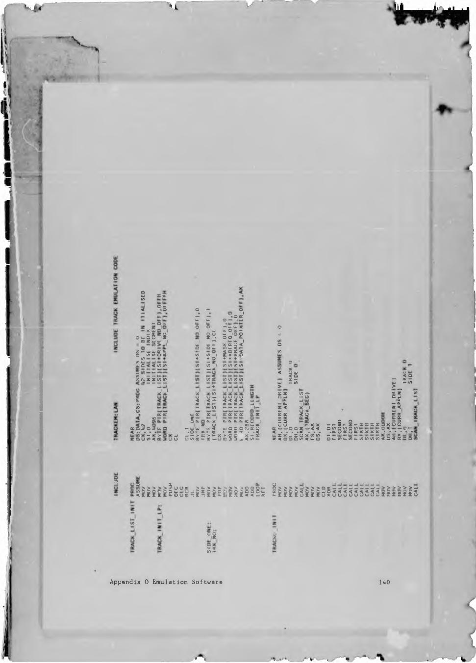
U v
§-J
Q%<
Z u.
®S
°££; tZ) w w C
*— o >•*-
I I j 8!w w or a.co irj o << < coco
d!/) - — coazzcoco
— — — —
tf 5 * 12sac oS < •• •
z o o
ct cc >o — w-O S u.1 o35 < i !
O •“ o— — o OC1u. w o -*• . UJ
O O —*1*. u. xI tu u. o — —8°. I i '- W w w
O o u.
CO CO I♦ •
CO to 1 CO to to COI*co 5— ♦.'S
U. lO O o c 'S.IUJ w |
S 2 3 Z2 5 5 2 + + + ;
to CO CO to
u d
^ 5 = %% % % : :a x - x x x x u .»- co #-#-»-#- ik-UJ X X - X X X X X *
XX X x X X ec u iC W X
UJ O C O CNi X O_ _ ►- x x r - »<w — > x > K X > c g x - x v to x - x w(j x 5 5 < to i-
* = . u^ UJ Ud lUd <
• o *- Jt *- X
oasto
to<u>
:IIK* W —n _i — o
h'X— XJ",IIu o i— x x -K — — O O Z — < < O
< • » » »dr » » * *UjXX-ZOXV)^ -r « to a o (7) « w a o
o of- X ► ■ Xv) o v) o z u z uu. V) u. IZ)
>- s s s x a w ax x x x * •u. V) (Z) V) V) <
- IsW — CO >$! .— X
2 < i11 i5 ® B a . =H i - i l
to
I mJ mtJ tmJ mtJ wJ mm‘ ® > > > > > $ u u « > g. > > 6 . > >-» » o o g « - 8 > > > > u > > > o a c i L - j - - , - - . - - j - > > > > > > ^
:5 E i 8 k i 2 S u ^ ^ i ^ £ 8 E i ? £ $ i § 5 ! s £ £ $ £ E 5 i i £ d h 5 5 S 5 5 5 5 5 $ l $ z i £ 5
CO
= 8
35£2
Appendix 0 Emulation Software 140
/>
ooh-XuJQ
%*LUQ<QwX
go
u»oacwQZ
XwQC
Ow(/)
<H - x x-xxz»< X O »- *- K-. . . X X Xx c/) cz> — — —-< UJ O o V) l/> tz>
cruu-UUJI/)XUJa(/)uJ
OuwXsu .o6
XC\J o — XX OlACZ)< * »oUJ _J X »- Z < u </)
X X Xc X G\ oL C X SO o oX c o o in co X l*J x c o co< . • -o < . X < * - -oUJ _u u -J X N- UJ X X — X f- UJ _J -J X h-z < < < 0 ( 0 z u U Q O (0 z < < O CO
XO CO
cu xwo
> Kto
g § ww o
oUJ || Z X -JX
x < x c-J 5II o X w —- wX . W W W< o o X c W o
z z h 1 o o— o « n 1c o w i z c z cx Q I Z z110.— X w I X 1
< 10 w > w O w<0 — — X < oc o o Z X x X
o o C O < h- to10 W w C *f «♦* 1- 4w X XX co to CO toX II IItoCO x X O f - f-< X c _J ro CO to to
W W W wx ! X 1 X 1 X 1I 1 1 If- > w > *- > *-w QC •— X X —X — X *- X - X*— o z — o z — Z ‘-*
C\J I I 1 Z 1X o - y w - i — O X — w 1— Wl< - X x X < X *- O X f-w — X > X W C X U . > — — >z t O ( J X < Z 3 — z x c o z x
x a m x- i - j - j y u u x -J x y in yO > > tt. i~ 0 > 0 > 0 0 > > a - * - O > V) _i Q. O >- O > C > > a- h- O > > a a. o- £. c. a. a.
H"V)uX 1<a. 6" OO »- .. * * O*- 5 z u I uj i *</> O *- W X > -I X Ix u x k < — e. < o
— UJ — f — (J x x x —u. cn co c/5 o c/) o < ~ CO
Appendix 0 Emulation Software 141
Nz, m d § l
>QC
I 5*
Appendix 0 Emulation Software 142
„V'.. , , " W V t , „ ■ k
APPENDIX P THE TRACK EMULATION SOFTWARE
This routine forms the core of the entire disk emulation process. As its
name implies the routine controls the emulation of a track of data that
would normally be read off a floppy disk. This routine also accepts data
that would be written to the floppy disk. The track that has to be emu
lated is shown in Figure PI and is described in detail in Appendix A.
The track emulation procedure is described below in terms of a high level
language. Procedure names that are in capital letters relate to procedures
that can be directly associated with characteristic features of the track
of the disk as shown in Figure PI. Procedure names that are in small
letters are procedures that are required due to implementation details.
Bracketed procedures indicate procedures that have been split but con
ceptually should be one procedure. The assembler listing is at the end
of this appendix.
It is assumed that the communications controller has been programmed
previously See Appendix 0.
Appendix P The Track Emulation Software 143
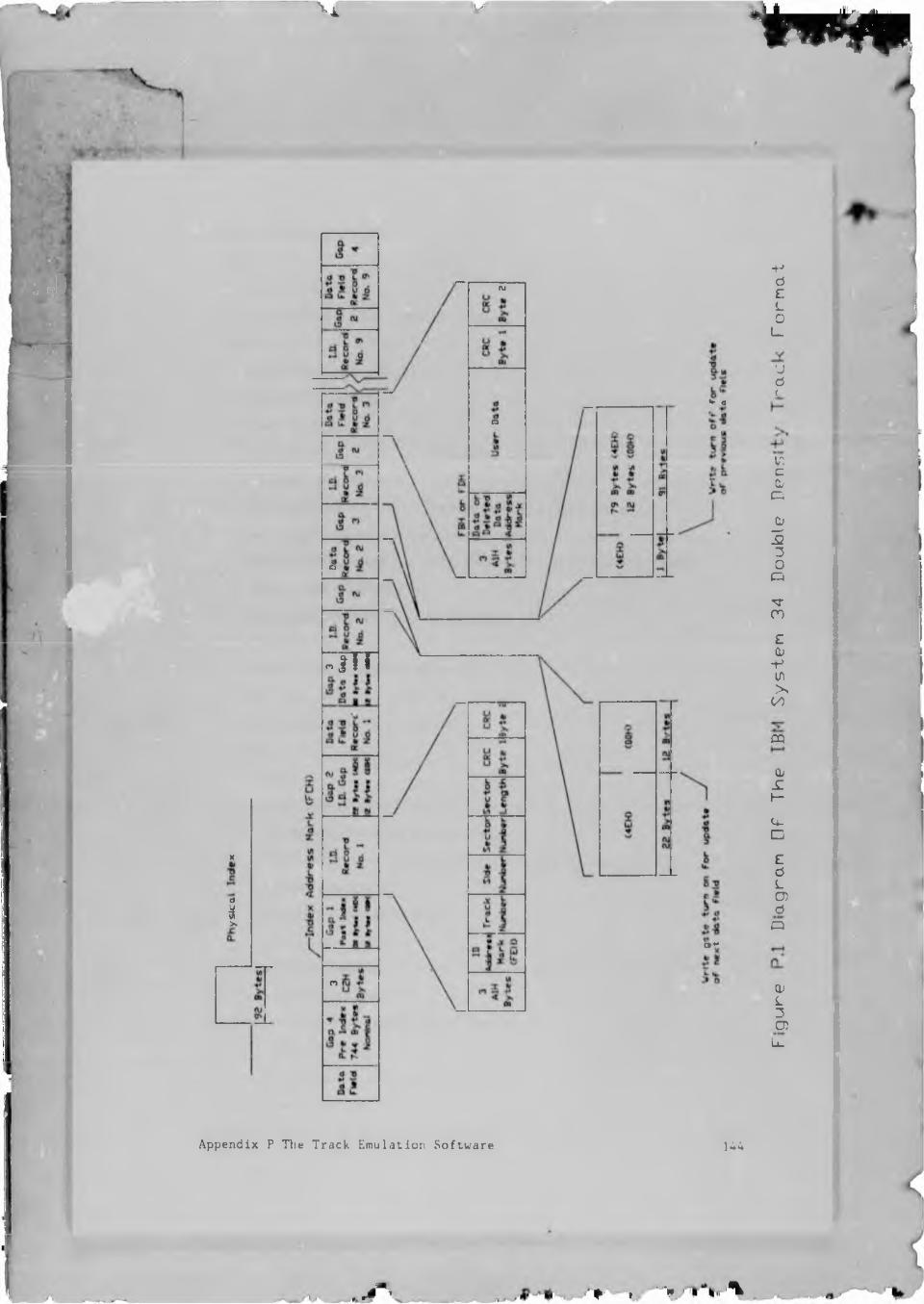
' 5#
X l V"
w w
:: 3.1
X
dI>.
rxj
u- da
o
mn
ce*'
m
•HdEL0L
Jd<.
incCL'C_Cj530Q
Vn
E(Li-Pin>>(/)
m
Hi_ch-
U-□£dLO)do
aiL3CDU.
Appendix P The Track Emulation Software 144
i
V - >■ -i / ■ > A
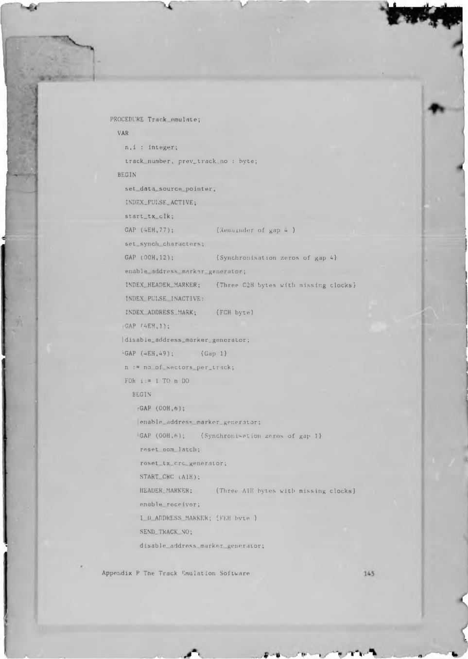
PROCEDURE Track emulate;
VAR
n,i : Integer;
track number, prev_track.no : byte;
BEGIN
set data source pointer,
INDEX_PU1,SE_ ACTIVE;
start_tx elk;
GAP (4EH.77); {Remainder of gap 4 }
set synch characters;
GAP (OOH,12); {Synchronisation zeros of gap 4)
enable address marker generator;
INDEX.HEADER MARKER; {Three C2H bytes with missing clocks}
INDEX.PULSE INACTIVE:
n :* no.of sectors per.track;
FOR i:= 1 TO n DO
BEGIN
'GAP (OOH,6);
enable address marker generator;
GAP (OOH,6); {Synchronisation zeros of gap 1}
reset com latch;
reset tx ore generator;
START CRC (A1H);
HEADER MARKER; {Three A 111 bytes with missing clocks)
enable receiver;
1 1) ADDRESS MARKER; {FEH byte }
SEND TRACK NO;
disable address, marker generator;
INDEX. ADDRESS.MASK; {FCH byte)
-GAP f4EH,1);
!disable_address_marker_generatcr;
LGAP (4EH.49); {Gap 1)
Appendix P The Track Emulation Software
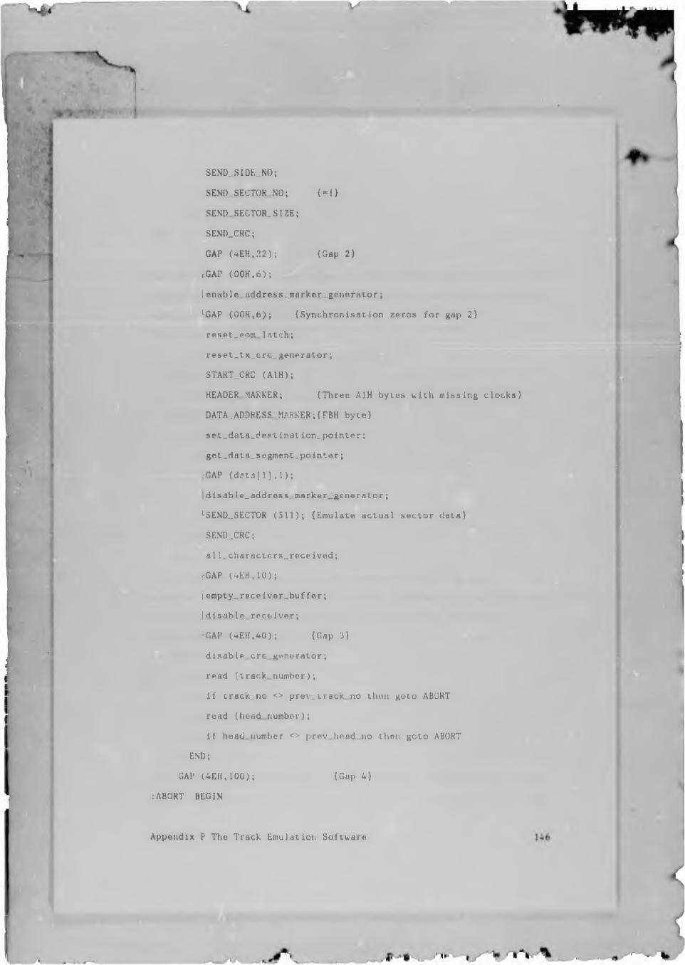
SEND.SIDF._NO;
SEND_SECT0R NO; (=i)
SEND SECTOR.SIZE;
SEND_CRC;
GAP (4EH.22); {Gap 2)
rGAP (00H.6);
I enable, address.marker_go.norfltor;
LGAP (OOH,6); {Synchronisation zeros for gap 2}
reset_eom latch;
reset_tx_crc_generator;
START„CRC (AIM);
HEADER MARKER; {Three A 1H bytes with missing clocks)
DATA_ADDRESS.MARKER;{FBH byte)
set_data_dest ination_pointer;
get_data_segment. pointer;
-CAP (d<?ta[l),1);
disable_address. marker_gcnerator;
LSEND..SECTOR (511); (Emulate actual sector data)
SEND.CRC;
all_characters_rece ived;
rGAP (4EH,10);
!empty_receiver_buffer;
|disable receiver;
LGAP (4EH.40); (Gap 3)
disable crc generator;
read (track number);
if track_no <> prev,track no then goto ABORT
read (head number);
if head number <> prev head no then goto ABORT
END;
GAP (4EH, 100); {Gap 4)
:ABORT BEGIN
Appendix P The Track Emulation Software
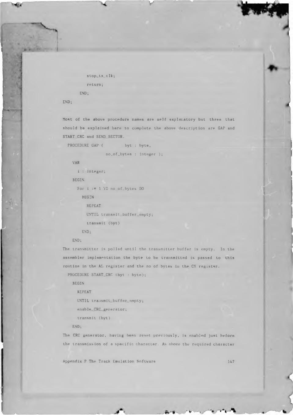
stop_tx_clk;
return;
END;
END;
Most of the above procedure names are self explanatory but three that
should be explained here to complete the above description are GAP and
START. CRC and SEND SECTOR.
PROCEDURE GAP ( byt : byte,
no_of_bytes : integer );
VAR
i : integer;
BEGIN
For i :» 1 TO no.of.bytcs DO
BEGIN
REPEAT
UNTIL transmit. buffer_cmpty;
transmit (byt)
END;
END;
The transmitter is polled until the transmitter buffer is empty. In the
assembler implementation the byte to be transmitted is passed to this
routine in the AL register and the no of bytes in the CX register.
PROCEDURE START CRC (byt : byte);
BEGIN
REPEAT
UNTIL transmit buffer empty;
enable CRC generator;
transmit (byt)
END;
The CRC generator, having been reset previously, is enabled just before
the transmission of a specific character. As above the required character
Appendix P The Track Emulation Software 147
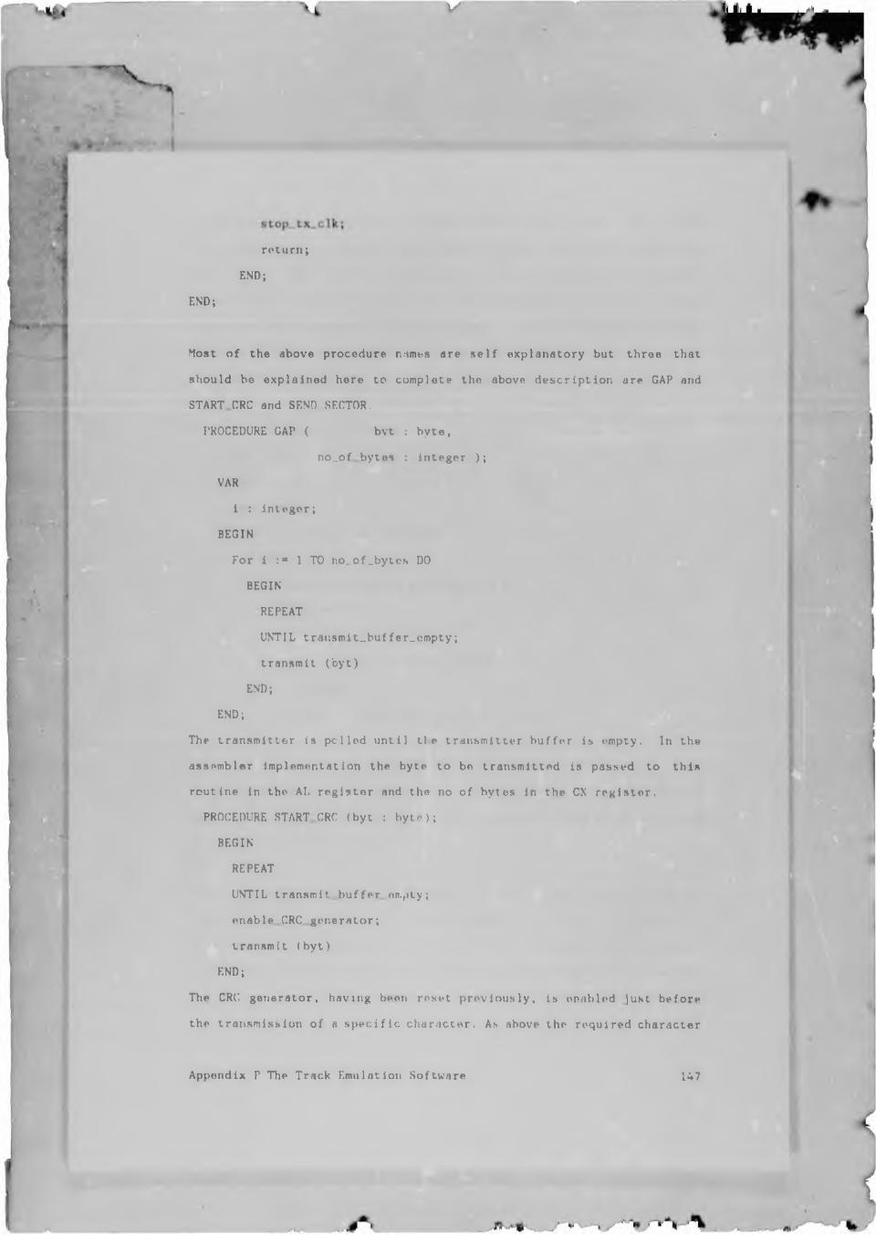
return;
END;
END;
Most of the above procedure names are self explanatory but three that
should be explained here to complete the above description are GAP and
START CRC and SEND SECTOR.
PROCEDURE GAP ( byt ; byte,
no_of bytes : integer );
VAR
i : integer;
BEGIN
For i :* 1 TO no_of.bytes DO
BEGIN
REPEAT
UNTIL transmit_buffer_empty;
transmit (byt)
END;
END;
The transmitter is pci led until tie transmitter buffer is empty. In the
assembler implementation the byte to be transmitted is passed to this
routine in the AI. register and the no of bytes in the CX register.
PROCEDURE START CRC (byt : byte);
BEGIN
REPEAT
UNTIL transmit buffer empty;
enable CRC generator;
transmit (byt)
END;
The CRC generator, having been reset previously, is enabled just before
the transmission of a specific character. As above the required character
Appendix P The Track Emulation Software 147
is passed to the procedure in the AL register. The transmit CRC enable
bit should be in the desited state when the data character is loaded from
the transmit data buffer into the transmit shift register. To ensure the
proper state of this bit, the buffer state is monitored until it i$ empty
i.e. the data would have been transferred to the shift register and only
then is the CRC enabled and the data character loaded.
PROCEDURE; SEND.SECTOR (no of bytes : word);
VAR
i.RxD.CHARS : integers;
byt : byte;
BEGIN
RxD.CHARS := 0;
For i ;= 1 TO no_of_bytes DO
BEGIN
IF char.ready AND (RxD_CHARS <512)
THEN BEGIN
receive (byt);
RxD.CHARS :* RxD.CHARS + 1;
END;
IF tru smit buffer empty THEN send (byt)
END;
This procedure is responsible for transmitting the sector information
during the emulation process wHle at the same time accepting data that
is being written to the sector.
Most of the above mentioned procedures can be followed easily in the as
sembler listing at the end of this appendix. Only aspects of particular
interest and importance will be discussed. The constants used will be self
explanatory in most cases but all constants used are defined in Appendix
0. The peculiarities of programming the SCC will also be described there.
Ap endix P The Track Emulation Software 148
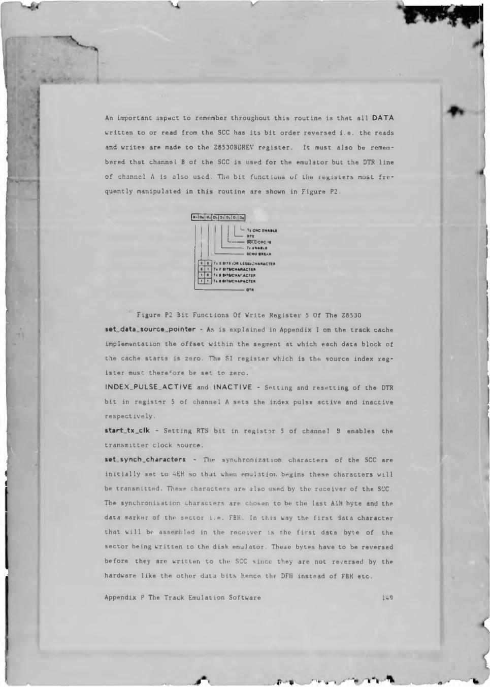
An important aspect to remember throughout this routine is that all D A T A
written to or read from the SCC has its bit order reversed i.e. the reads
and writes are made to the Z8530BDREV register. It must also be remem
bered that channel B of the SCC is used for the emulator but the DTK line
of channel A is also used. The bit functions of the legisters most fre
quently manipulated in this routine are shown in Figure P2.
|p.io.]o,fp.|t),!o,(o,[5
Lt - T« CMC I N A iU — AT*
L.'. nrc&c*c<i---------- ft «NA*ll
------------------------ IC N O M tA A
T« I i l t l 10* K U k C H A A A C T t*T i I SITWCHAAACTl*
T l * AITt/CHAf.ACTIA T i i •ITKCH AA4C TIA
------------------------ - OTA
Figure P2 Bit Functions Of Write Register 5 Of The Z8530
set_data_source_pointer - As is explained in Appendix I on the track cache
implementation the offset within the segment at which each data block of
the cache starts is zero. The SI register which is the source index reg
ister must therefore be set to zero.
INDEX_PULSE_ACTIVE and INACTIVE - Setting and resetting of the DTR
bit in register 5 of channel A sets the index pulse active and inactive
respectively.
start_tx_clk - Setting RTS bit in register 5 of channel B enables the
transmitter clock source.
set_ synch .characters - Th" synchronization characters of the SCC are
initially set to 4EH so that when emulation begins these characters will
be transmitted. These characters are also used by the receiver of the SCC.
The synchronisation characters are chosen to be the last A1H byte and the
data marker of the sector i.e. FBH. In this way the first data character
that will be assembled in the receiver is The first data byte of the
sector being written to the disk emulator. These bytes have to be reversed
before they are written to the SCC since they are not reversed by the
hardware like the other data bits hence the DFI1 instead of FBH etc.
0 00 11 01 1
Appendix P The Track Emulation Software 149
enable_address_marker_generator and disable ... - Setting and resetting
the DTR bit in register 5 of channel B enables and disables the address
marker generator.
reset_eom_latch - For the CRC to be appended to t block of data this latch
has to be reset after the first data byte of the block has been loaded.
When this latch is set again when no more data is supplied at the end of
the message the CRC is automatically appended. This is done by issuing
the reset EOM command to register 0 of channel B.
reset_tx_crc_generator * The CRC generator has to be preset before the
calculation of the CRC on the forthcoming data stream can be performed.
This is done by issuing the reset Tx CRC command to register 0 of channel
B.
SEND_CRC - The SCC is forced to send the CRC calculated on the data
by causing the transmitter to under-run i.e. stop providing the trans
mitter above. The EOM (End Of Message) latch must have been reset at some
stage between the first and last character being loaded into the trans
mitter. The way that this is done here is by forcing the program into a
loop after the last character of a block is sent. This loop is terminated
by the EOM bit being set which indicates that the transmission of the CRC
is in progress.
set_destination..pomter - The source pointer is cons m i ly updated
throughout the emulation of a track of data. The destination pointer is
only updated during a disk write operation and since not all the sectors
need be written to. The destination pointer is therefore updated at the
start of each sector of data in anticipation of a disk write.
get_data segment.pointer - As explained the track cache index stores the
segment at which the data starts. The data segment register is loaded with
this value.
all_characters_received - Characters are loaded from the SCC until the
full sector being written to the emulator has been read in.
Appendix P The Track Emulation Software 150

When the assembler listing is examined the gap sizes implemented in the
program are actually smaller than those specified in the high level de
scription. As was mentioned previously the gap sizes were reduced as much
as possible to increase the efficiency of the emulation process. The only
gap size that could not be teduced is that of gap 2 between the sector
I.D. and the actual sector. When this gap was reduced ('ata being written
to the disk was lost at the beginning of the sector. This gap therefore
is best left the correct length. The Floppv Disk Controller did not appear
to be affected by the reductions in the other gap sizes.
n
Appendix P The Track Emulation Software 151
V S
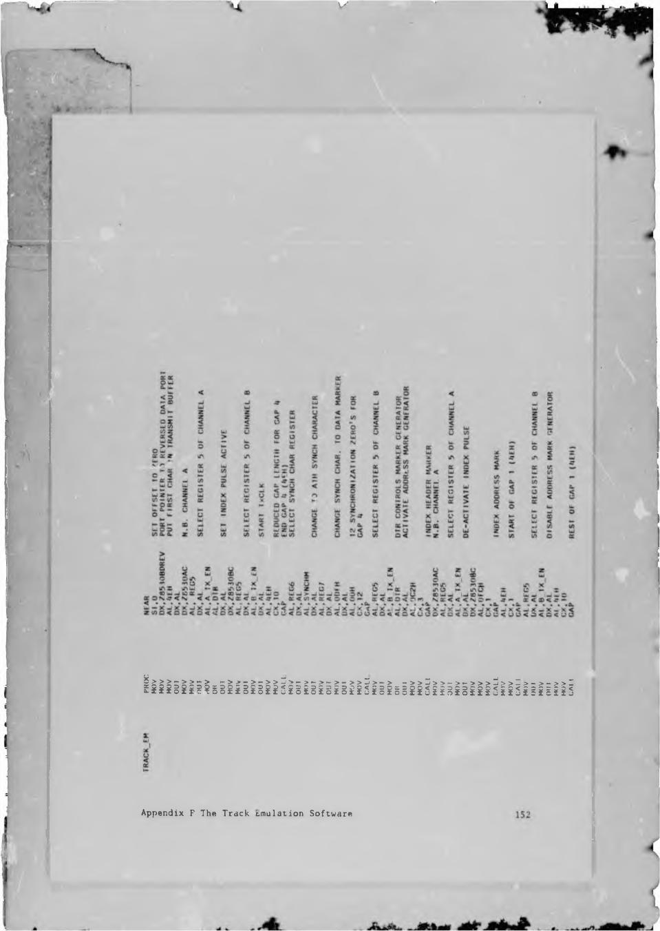
v
iiiiiiiiiiiiiilliiilllilililiiiliiliiiliiiiiiliiiiliilili
Appendix F The Track emulation Software
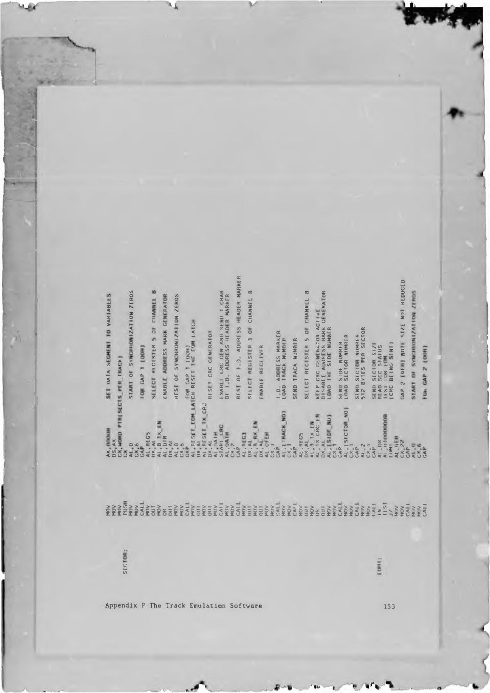
' H
w5I
x
<?
V)§wNzO<N
5
>V)C/)2 h o a.
5
t/) u.
ruo
acwV)cUiK
5
O -
IV)V)
I1/5 W
XH 3X
V) X 1 X X X 8< X X o 3o Z W •J -J uX u x X w u < XLU X UJ z z XN
- 2o z z< < < > z c
z e 1 zo z Z X z G u N- Ou G UJ
5? o V) < X X X N.< < £ < </> o X o X w oN -J o O UJ u. UI
g g gX X — V5
z z X m ^ X X J> u. UI Gi
< <i
X UI — ►- 3 X X X u Ui *—X t/> X X < X X X •x ic z u x X (A n m •—X Z UJ — Z V) < Ui I X X UI X VO X 3 3 — 3 Z czg w z > D 3 X Z Z X i/5 — U z
G X V) t/3 Z z V) Z X o 3 wz w X G 3 o w tn Wh. 3 — G 3 1/5 x g> w S G o ui z *• G O I/; u. Gc/> U i < u1
w < W N- *- 1/5 N- Z uu X u X X X G U 3 G G w G G X - a-u x W u u o a: X X w Z — UJ UI *- u U O ui V5 G w- Xo 5i2 u Q O w < f- H u G - i- V) tn V5 >u u — G X X <NiX X - u X ■ o O w X < Q 0 3 o C 3 - G(/)g z
00 < C/5 «J < °.§ z —1 ui (A < z < zeu Z < 1/5 X Xw u ^ !Z w u z H UI u C «— •* m. u G <X u U X uu O X V, Lw — _i c/> V) x C — V5 -i in jy 1/5 X — w G
) X <><: 0\c
5S u u< u
r xO XUI U IN- u QC<XO<
< Jx J JxO < C < < Q
T)g
ia in —U U U -J <Ovc a < a: < c
-J x < - x u x* —< u o < o < o <
; u :
i =
w 3u,g
£ 2 ° ,- U U IX —— X < ffi »- <
soou(/)
X O ^ X < X < o — X < X »—•— Ow *—<X • »X • • » » » * Q. » • X • • • • » » »X % * X » *• - - J X < - J X U X - / X < ^ X < U X U - Z X U X < U X < - J Xi n < u o < o < Q < u o < u o < c x < o < o o < u o < u
X «-rw c r — t\jCL » * X » »X » e X
< — 5 u x ,O < < w < o o- < u S
> > > i«> > _j>>-> - > > - > - > - > r > > _j> - > - > > _i> > r >-> - > > _ > > - > > ! v > > " > > zl i i s i i S i S E g g i i S i S i i i S S i s i S i B i i S i i s i s i B g i i S i h i S S E r ^ I i s i i S
Vw1/1
Appendix P The Track Emulation Software 153
rVx. I H P I wHb- 'I
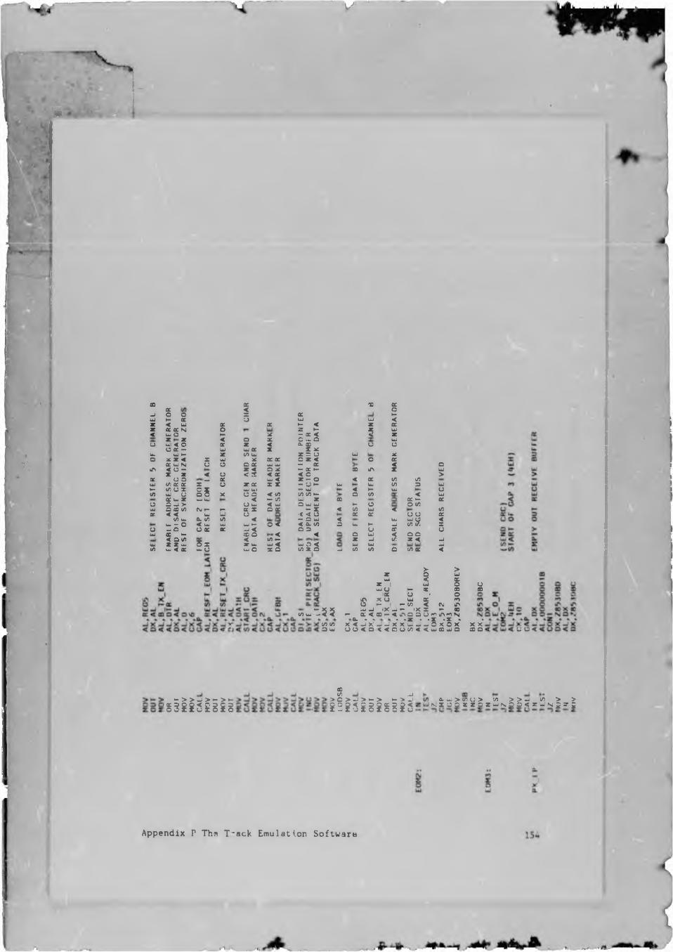
V
*
A
CD QC ro XK < o-J O O X X h-W H CC u UI UI <z < UI oc QC k- < z Xz QC QC N o z K z Ui< ui O H )C - X < 1 zz z < o X O u .Q wu u < O CC z < CV CD o oO CC - UI w CC X X Xu. w u- z to W Z 3 u w JCo X z < X UJ ac X X o z < o Xa: uj n u o o CC W UJ - X < Difx < o - z < a x t- X u. X lA X wX Z < u < X < X < o >X u o 02 UJ < Z •— O < X V) l/>
Ui IS) CZ X x “- u z a: X X - U K UI UJ to 3 Wk- to u X C I UI Ui *— w < t— UI Otn u, u o 5 X o o < t/> 10 CO u. o to < UICC UJ z - LW < — v> u. Z CD X H- XO S u > O UJ < UJ O w ui u o o tow O tfl V) CM #- k- a x Q X - X < (0 w < toar. < < UJ — O < 4 0 X X o o X</> U 0l 05 to < — O UJ < UJ UJ O <u. — c < UJ u. w *- O < < CL t0 a u H u to t7; X
u -JO O K QC - j < C 3 o X Ow CD k- CD O < < Q UI < O Q< QU) < CO N- Z -J to z < _J
w z z ^ 5 x Z u. UJ < ui O < Ui w u(/) w < Z u- c w O x a </5 Z O «j to to o to X <
> >5 S £
Z I w o uuj u — cc n cdIK O I Oin X u Ui k mo »— i »-1/) < N nuj u ix-i— ix i - ®a:<coi-<iAaoornirM^N& * * - JC • »X ‘X *COCrt X < - I X ' - , - . X X U ---------1 O X O X X XO W U 0 < 0 < < 0 0 t / ) < < u j a 3 u j 0 CD o
v) w *3.5 5 —
• - > > - i > i - > f - :!§ 3 £ i 5 £ § i g i
$ i->d' > O > _l > •- >! £ 2 £ 5 i 8 i § § i 5
a. ^, > v> t ; > V) > > _ . V) > >n. x c c z z o s u i N O O c z - x s r ;
Appendix P Ths T~ack Emulation Software
c o<
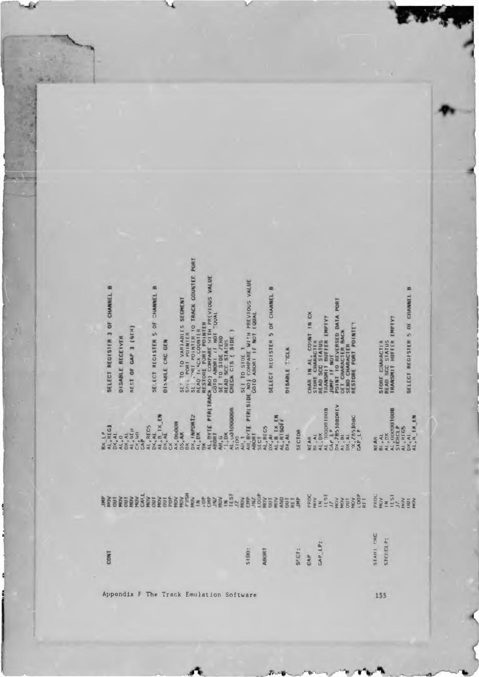
^ 4
■C)
V)o
5
s >Xw
o
</)
owQC 8
V)wacs 5-i v)
v> ow — a:- j tr w 20 u, OC •-<»- — z
lil!O M- o ¥- ac — *o h c
II• x
v>8> < IU<L UJ
Z % tZ)j u. N ►-<:I
m
w Q► -V •< WQ'WW I/) V) VS K
S - < 2
foO
rr
) *-f ugo8
S 5 -:00V)owX
in z- o 2%=,S in
m wM
O Sa. uj — — w c-JOC < o< 3 sS 5a: < m <
X ^ 2 ^ 5 ^ S 5 ^ 2 < 5 5 5 8 8 5 ^ < <5.8< in
>• £w •.< I*— -J• «o o
5 5 < S < § < < 5
r z in x in z — 3 w
x in z
o in xo in x
§aV)
>X w1 1 - 8c o Oo ^O X u> f\x
u x c ^ -J 00 Ux < o n IN ® < N 1< • * X * » • »Xl w _ _ l _ , < x _ i x x <z o < < o o < o r ' 0
- i x 5 c — ie<CJOa:s:<eu. j — — x * C D < < V > < 0 <
8 > Zr CL>><- > o >-2 i E ^ ^ $ $ 8 E 8 i
8 > £2 E 5 Z
> - >^£ = $
8
inxs
X •JI 8
V! V)
Appendix F The Track Emulation Software
_ . > -•"■>.
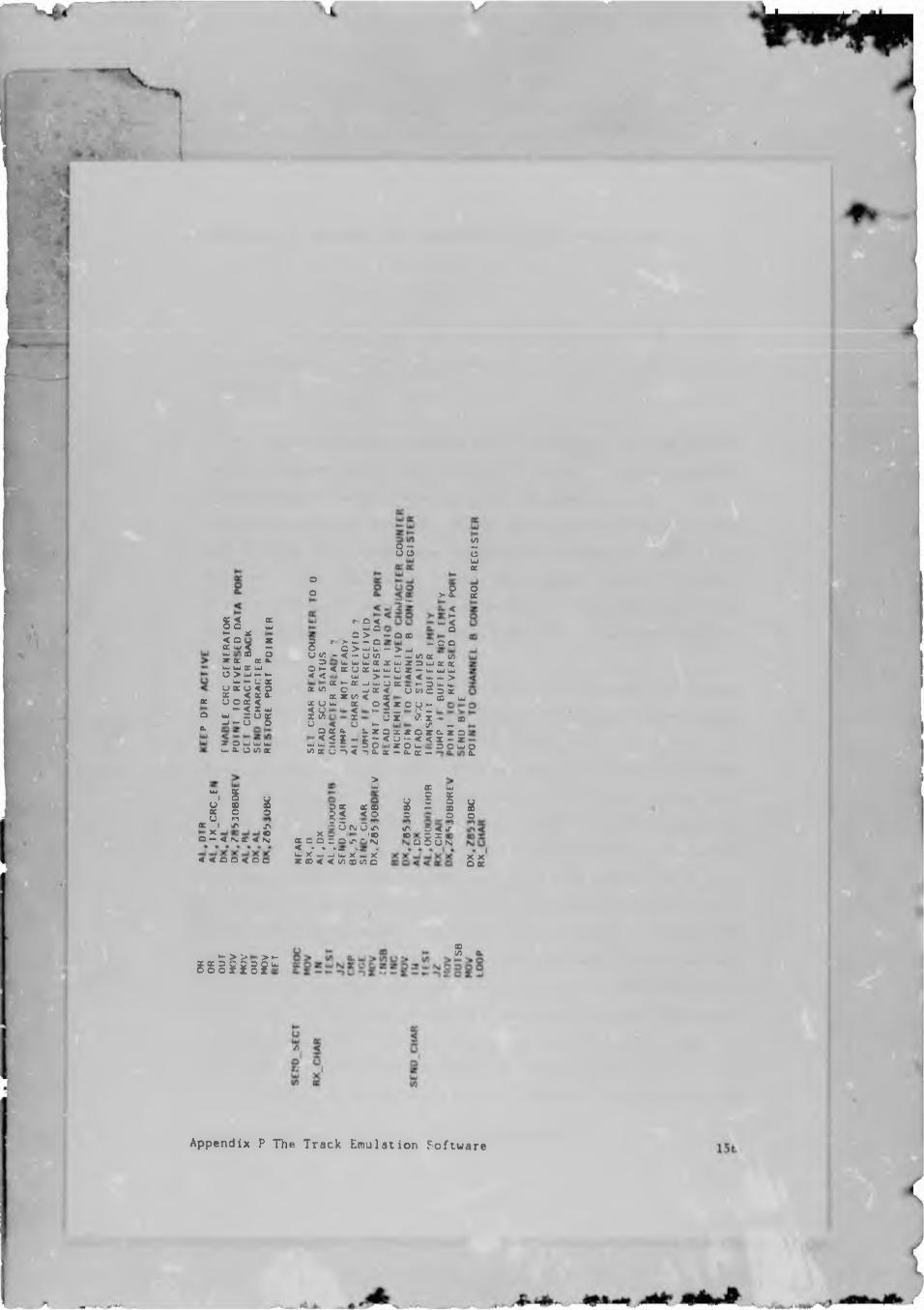
cra
Q.
g< oc O O yjM- ^22 < 5uj od oz x cc cl w w o: w O > w »- t-w # - u %
m u^i-5u B7 O UJ u UJw a. o a:
oo
§U (C :si;' - !::« £• OC k-o: tn o x z
P “ “s— U.U> Xilu ->
r* O < <— O3 >urf — Q> w W— o co wu.cc U % w W >a: - j u.
i'fi i i
8 5
- Q flD- > -j
— — ^ cr% w z 3 w uj U Z — ^— uj < < »*.3 = o % g l f ° H rU X CA X
> 2
-I- C O
VO
5wcr
§
<7. x - it »-
V)q: ocw wU. >W. UiE ' w
— CO
§ 5 f § l « 5 £ £ =
6- Z O§ 5 5 s
1i' I Iet i j \ jno < N r < 5< < Q Q < C Q
>UJ
j l ...•- o M u ir5S
1(0OiAONX _x z a z < • • «— - — . U X - J U U J X w X Z S 3 < < V ) 0 0 V ) O
§ =
OR w $ !ir d < j-® o S 5 n
%o
2 2
$g g U g § § :
Appendix P The Track Emulation Software

APPENDIX Q TESTING THE FLOPPY DISK DRIVE EMULATOR
Teslinji u unit such as the floppy d'sk drive emulator requires a modular
testing approach so that the number of variables in each test is
minimised.
The unit can be divided into three modules tor testing the MFM decoder,
the microprocessor control unit and the MFM encoder. A brief explanation
of the testing of each of these units will be given.
Olivetti M24 Personal Computers provide the facility for the user to in
sert a 2ilog 28530 Synchronous Communications Controller (SCC) on the
motherboard. Only one channel of this dual channel device is hardwired
to the RS 232 serial port with the other free for use. Using two P.C.'s,
one of which should be an Olivetti to provide the above mentioned feature,
the MFM decoder can be tested.
The MFM decoder has two inputs viz. the Write Enable and Write Data inputs
that require connection to the floppy disk drive interface and two outputs
providing a synchrtnous clock and data output. The decoder inputs are
connected directly to the write enable and write data lines on the floppy
disk drive interface. The outputs are connected to the RxD (Receive data)
and one of the clock inputs on the SCC. A short assembler program was
written for the Olivetti P.C. which initialises the SCC and then enters
a polling routine to read in characters and display them on the screen.
To ensure that no characters are missed, the characters are written di
rectly to the screen memory. The synchronisation characters used ar 4F.H
characters. Note the synchronisation characteis must be written with
tleir bit order reversed. The cnip initialisation is the same as described
in Appendix 0. Using these synchronisation characters the SCC should begin
assembling characters, two characters alter the write enable signal be
comes active. A disk is then formatted in the normal way on the P.C. to
which the inputs of the decoder have been connected The program on the
Appendix Q Testing the Floppy Disk Drive Emulator 157

Olivetti P.C. should be started first so that the SCC is initialised and
'hunts’ for synchronisation characters. When the format program is
started the SCC will synchronise on the characters in gap 4 preceding the
index address marker. See Figure PI. The characters being written to the
disk being formatted are written to the screen of the Olivetti BUT their
biw order is reversed i.e. instead of N's appearing (ASCII character
corresponding to 4EH) wo find r's (ASCII character corresponding to 72H)
Beside testing the operation of the decoder, the format information
written to the disk during formatting could be verified. The CKC charac
ters were also of great use as will be described later.
The synchronisativ.ii characters wore then changed to A Hi and FBH respec
tively. These two characters are the characters immediately preceding the
data written in a sector. (Again these two characters must be written with
their bit older reversed). Using the same program as above on the Olivetti
P.C. with the minor change in the synchronisation characters. PCTOOLS was
run on the other P.C.. Again the Olivetti's program is started first and
then individual sectors were written to the floppy disk drives. (Note in
this test and the one described above a i >rma 1 floppy disk is being
written to. Which disk drive is used is of no importance since the Write
Enable and Write Uata signals connected to the decoder are common to all
the floppy disk drives). This test was done to see if the choice of
synchronisation characters would be suitable for the SCC receiver on the
emulator. This choice of synchronisation characters require* no inter
vention from the CPU to separate the data. The data appearing on the
Olivetti screen was compared with that being written using PCTOOLS. Using
synchronisation characters of AIM and FEU the I D. records of each sector
could be checked during the formatting process. This proved to be very
useful in the CRC checks as is explained later.
These tests verified the operation of the MFM decoder hardware as well
as verifying some aspects of the software (or the emulator. By using this
Appendix Q Testing the Floppy Disk Drive Emulator 158
Olivetti P.O. should be started first so that the SCC is initialised and
'hunts' for synchronisation characters. When the format program is
started the SCC will synchronise on the characters in gap 4 preceding the
index address marker. See Figure PI. The characters being written to the
disk being formatted are written to the screen of the Olivetti BUT their
bit order is reversed i.e. instead of N's appearing (ASCII character
corresponding to 4F.H) we find r's ' ASCI I character corresponding to 72H).
Beside testing the operation of the decoder, the format information
written to the disk during formatting could be verified. The CRC charac
ters were also of great use as will be described later.
The synchronisation characters were then changed to A1H and FBH respec
tively. These two characters fre the characters immediately preceding the
data writtun in a sector. (Again these two characters must be written with
their bit order reversed). Using the same program as above on the Olivetti
PC. with the minor change in the synchronisation characters, PCTOOLS was
run on the other P.C.. Again the Olivetti's program is started first and
then individual sectors were written to the floppy disk drives. (Note in
this test and the one described above a normal floppy disk is being
written to. Which disk drive is used is of no importance since the Write
enable and Write Data s.'gnals connected to the decoder are common to all
the floppy disk drives >. This test was done to see if the choice of
synchronisation characters would be suitable for the SCC receiver on the
emulator. This choice of synchronisation characters requires no inter
vention from the CPU to separate the da' i. The data appearing on the
Olivetti scieon was compared with that being written using PCTOOLS. Using
synchronisation characters of A1H and FEU the l.D. records of each sector
could be checked during the formatting process. This proved to be very
useful in the CRC checks as is explained later.
These tests verified the operation of the MFM decoder hardware as well
as verifying some aspects of the software for the emulator. By using this
Appendix Q Testing the Floppy Disk Drive Emulator 158
Vi v
test configuration tlie area where hardware problems were most likely was
restricted to the decoder.
Testing of the microprocessor control unit was done by testing sub-units
within the control unit. The first sub-unit tested were the diagnostic
L.E.D.'a since they couldn't fulfil their purpose until their functioning
had been verified. The memory test described in Appendix 0 could then be
performed. The input port that is used foi the track counter was tested
by applying various inputs to this port which was then output on the
L.E.D.'s. The Olivetti P.C. was used in the testing of the control unit
as well. Each of the SCO's on the control unit were tested by sending
messages from the control unit to the P.O.. The P.C. was using the same
program as described above.
At this stage the MFM decoder could be combined with the control unit.
The one ECC's receiver was thus connected to the MFM decoder in the same
way as it had been connected to tha SCC in the Olivetti previously. The
second SCC was connected up as a transmitter to the Olivetti P.C.. The
software required for this tost was a combination of the software lined
up to this stage. The program written for the Olivetti for the first
formatting test was implement# on the cont;o1 unit along with the program
to transmit data to tho Olivetti P.C. . This sotiwaro was combined in such
a way that a block of data was read into the control unit which was then
transmitted to the Olivetti. The connections to the inputs of the MFM
decoder were th" same as in the original tests. The tests tnct had been
previously performed on the MFM decoder were repeated. In this case though
the data appearing on the Olivetti screen is not hit reversed since the
bit order is restored by the control unit hardware. The original results
obtained with the MFM decoder and Olivetti alone were now verified with
the control unit included.
This cc’.firmed the operation of the MFM decoder with the control unit.
Appendix Q Testing the Floppy Disk Drive Emulator 159
Testing of the MFM encoder required the use of a logic analyser as well
as the Olivetti P.C.. The SCC on the Olivetti provided the inputs to the
MFM encoder. The data inputs to the MFM encoder as well as its output we,^
monitored on the logic analyser. The encoding of all the bit sequences
that when encoded produce all the possible MFM coding combinations ware
tested. These combinations are described in Appendix F. Sequences of zeros
followeo by the characters in the Index and I.D. address markers were used
tc verify the operation of the address maik generator. This required some
control to be included from the software level. Recall that the address
mark generator is controlled by the DTK line of the SCC. The waveforms
recorded with the logic analyser corresponded with those of data being
read off a typical floppy disk as required.
Having verified the encoding of the data only the CRC generation had to
be verified. This proved to be rather difficult and time consuming. The
main reason for this being that the manufacturers data either doesn't
specify which CRC polynomial is used or what starting conditions arc used
or exactly what data it is calculated on. Some of the data that is
available is in fact incorrect. In an Intel application note entitled 'An
Intelligent Uata Base System using the 8272' |9) the following statement
is made in their discussion on the sector I.D. field. "The first byte of
the field is the I.D. address mark. The second, third and fourth bytes
are the cylinder, head and sector addresses, respectively, and the fifth
byte is the sector length code. The CRC character is derived by the
controller from the data in the first five bytes". As it turns out this
is not the case. The Western Digital corporation have the FD1731/2 Floppy
Disk Formatter / Controller that can be programmed to operate as a con
troller for the IBM System 3a Double Density format tiiigj 10) , This format
it thoulu he recalled is the format used on the PC.. The data sheet for
the. FD1791/2 states that the polynomial used is x “ + x*1 + x* + 1. It
also states that the CRC register is preset to ones before the data is
shifted through it. This information was found to be correct. It also
Appendix Q Testing the Floppy Disk Drive Emulator 160
states that the CRC includes all information starting with the address
mark up to the CRC characters. In a figure in the datsheet the I.D.
address mark is shown to he the FEH byte In the data listed to format
disks for the IBM format the data byte written to produce each of the AIM
bytes required (which have missing clock pulses) states that the AIM byte
is written in MFM and the CRC is preset. Comparing this information then
with that from Intel it would appear that the CRC calculation commenced
with the T.D, address mark in the case, of sector I.D. 1 a and the data
address mark in the case of sectors of data.
Armed with this information the SCC in the Olivetti was initialised to
use the above mentioned CRC polynomial and initial conditions. The uata
in some of the sector I.D. 's that wet e read during the testing of the MFM
decoder were sent through the SCC and the CRC generated. (Note the SCC
was in loop-back mode so that the resulting message and CRC could be ex
amined on the screen). The CRC charactotw generated did not agree with
those read using the MFM decoder. A number of these sector I.D.'s were
tested and none produced the required results. Finding patterns in the
results obtained to try and determine the reason for the discrepancy is
virtually impossible.
Some of the CRC1s generated were verified by hand calculation. The results
of the hand calculations corresponded with those of the SCC.
The first attempt to rectify the problem was to reverse the bits of each
of the data bytes before calculating the CRC. Ttiis unfortunately just
generated a third sot of values. Working on the assumption that the
polynomial and the initial conditions were correct. the only reason for
an incorrect CRC is that the data on which it was calculated was incor
rect. Tliis assumption was made since the CRC polynomial used in the 8271
Single Density floppy disk conti iior |11) was the same and likewise the
82062 Winchester Disk controller!12] used this polynomial. An application
note entitled 'Hard Disk Controller Design using the Intel 8089'|13]
Appendix Q Testing the Floppy Disk Drive Emulator 161

states that this polynomial is ussd thore as well. The polynomial there
fore seemed a popular choice for this type of application.
The data passed through the gnnerntor was varied by adding and leaving
out bytes, reversing the data etc. The solution was eventually found to
be that the 3 A1H bytes preceding the sector l.D. address marker had to
be included in the CRC calculation. The data must also be presented to
the generator most significant bit. first. The 3 A1H bytes preceding the
data address marker were included in the CRC calculation foi the data
sector. Fortunately ihe resulting CRC corresponded with that of the floppy
disk controller.
The final sub-unit that required testing was the track counter. This was
done by connecting the STEP and DIR linos to the floppy disk interface.
The control unit was programmed to read the track com.ter input port and
put the value raad out on the diagnostic L E D.'#. When a disk is for
matted using MS-DOS 2.111s format program the track numbers arc displayed
on tne screen as formatting takes place. The values on the L.E.D.'s were
then compared with those on the screen.
Software based or. the f< mat information available was written tc -mulate
a track of dcta i.e. the TRACK KM routine with full size gaps. Sen Ap
pendix P. The MFM decoder, encoder and controller unit wore then inter
faced to tl > y disk driv» cable via the interface unit. The floppy
disk drive mul.-.or was then connected in place of one of the floppy disk
drive units At cess to the emulator 11 m DOS returned a 'NON DOS DISK
F.RROR' This error indicated favourable performance by the emulator. Tiie
floDpy disk control 1« was thus ible to find the sector that it was
look inn for. Wh*»n the sector was read and DOS realised that it did not
correspond with the required DOS format the error was given.
Appendix Q Testing the Floppy Disk Drive Emulator 162

Track 0 of a floppy disk contains various pieces of information for the
operating system. This includes the bootstrap, file allocation table and
the disk directory. The sectors assigned to these pieces of information
are the following:-
Sector 1 - Boot record
Sectors 2 and 3 - First copy of the file allocation table
Sectors 4 and 5 - Second copy of the file allocation table
Sectors 6 to 12 - Directory entries
The sectors tnat the operating system reads when a directory of a disk
is requested were ascertained by intercepting a BIOS interrupt call. The
T\T 13H routine in tie BIOS is used for accessing the floppy disk con
troller from the high' r levels of software. A short piece of assembler
patch ci de was written that redirected this BIOS interrupt routine to a
short routine that prints the parameters passed to this routine on the
scree; before proceeding with the rest of the interrupt routine. In this
way the sectors required by the floppy disk controller can be seen. From
this information the sectors required to -•r wide a directory of a disk
for example were determined. All these sectors lie on the same track viz.
track 0. The information in these sectors was read from & physical floppy
disk that had just been formatted. This information is inserted in track
0 in procedure TRACK0__INIT shown in the. assembler listing at the end of
this appendix.
The TKACKO INIT procedure calls procedures FIRST, SECOND and SIXTH to
generate the data required. FIRST fills the first and third sectors and
fifth sectors with zeros. SECOND fills the second and fourth sectors which
contain the File Allocation Table. SIXTH generates the data for each of
the directory sectors.
When a directory was now requested the ’Files not found1 message was re
turned by DOS which had immense significance. This indicates that the
floppy disk controlle* has been able to extract data from the information
Appendix Q Testing the Floppy Disk Drive Emulator 163
being generated by the floppy disk drive emulator. To test the ability
of the emulator to store data written to it various write operations that
require the use if track 0 alone were performed. This includes making
directories (MKDIR) and removing directories (RMDT.R). These operations
require that the file allocation tables as well as the directory sectors
are updated. Tests using PCTOOLS were also performed where a sector is
read in from the emulator and the first and/or last characters say of the
sector were changed. The sector is then written to the emulator and then
re-read to ensure that the entire sector was being written correctly.
These test alone proved that the majority of the hardware was functioning
as required and the software used to control it also appeared satisfac
tory.
The final test that was performed was the following : - The track cache
was implemented in such a way that its contents were fixed i.e. it con
tained the first 21 tracks (i.e. 42 sides ) of a floppy disk. Track 0
was again initialised in a similar way to that described above. It was
now possible to emulate a floppy disk with approximately 180K of storage
capacity. Now it is possible to copy large files onto the emulator and
read them off again.
At this stage various experiments were performed in which the gap sizes
were reduced. Again PCTOOLS was used to modify the beginning and end
characters of the individual sectors. When the size of gap 2 is changed
characters are lost in the sector being written. This gap was therefore
left unchanged. The other gap sizes were reduced with no adverse effect.
A test was performed to observe the effects of simulated network operation
on the disk drive emulation process. It snould be noted that in the ori
ginal emulator design had only one SCC. These devices have two channels
Appendix Q Testing the Floppy Disk Drive Emulator 164

and it was originally designed for one channel to be used by the emulator
while the other was for the network.
the network channel was initialised to accep an external transmit clock
source and to transmit data in synchronous data format. The data that was
to be transmitted was accessed from a single memory location using DMA.
The external clock source was provided from a variable frequency
oscillator. Files were read and written to the emulator as described above
while at the same time the transmit clock frequency was increased. The
results of this test were hardly encouraging. The required transmit clock
frequency is between 1 and 1.5MHz but the emulation process was failing
at frequencies as low as 20kHz!. Occasionally the emulation process was
failing at lower frequencies. Closer examination of the problem with c logic analyser led to these conclusions :- The emulator software was based
on polling while the network data was being supplied using DMA. DMA cycles
can occur at anytime when the bus has not been locked by the central
processing unit. It was possible therefore for a read or write to be made
by the polling software on the SCC which would be followed or preceded
immediately by a DMA access on the same device. The SCC has a certain
access recovery time i.e. a minimum period is required between the ac
cesses to the SCC. In the situation described where two accesses were made
on the SCC one after another this access recovery time was not met. In a
number of cases this corresponded with the failure of the emulation
process. For this reason a second SCC was added for exclusive use by the
network. When the tests were performed now the network transmit clock
frequency could be increased to within the required range without any
adverse effects on the emulation process.
The floppy disk drive emulator thus performed as required with file access
times slightly shorter or the same as that from a physical floppy disk.
Appendix Q Testing the Floppy Disk Drive Emulator 165
\ 4
LIST OF REFERENCES
1. Haugdithl, J. Scott 1 Local-area networks for the IBM PC' BYTE Vol. 9
No. 13 Dec. 1984 pp. 147 - 174
2. Abraham, R and Munro.R 'Microfloppies battle for pre-eminence1 COM
PUTER DESIGN Vol. 22 No. 1 Jan. 1983 pp.119 - 126
3. INTEL 18272A Single/double density floppy disk controller' MICROSYS
TEMS COMPONENTS HANDBOOK Volume 2 1984 Order No.230843 pp. 6-553 -
6-571
4. INTEL 'iAPX 86/88, 186/188 User's u mal Hardware Reference' 1985
Order No. 210912-001 pp. 2-1 - 2-32
5. Chaney,R and Johnson,b 'Maximising hard-disk performance' BYTE Vol.
9 No. 5 May 1984 pp. 307
6. McKeon, Brian 'An algorithm for disk caching with limited memory'
BYTE Vol. 10 No. 9 Sept. 1985 pp. 129 - 138
7. 'IBM PC Technical Reference Manual' First Edition (Revised March 1983
) Part No. 6936844
8. 'l.B.M. Disk Operating System ' First Edition (Revised May 1983)
Version 2.00 Part No. 6183485
9. INTEL '82530 SCC Technical Manual' July 1984 Order No. 230925-001
10. 21 LOG '28530 Data Sheet' 1983/84 Data Book Order No.00-2034-03 pp.
409 - 429
List Of References 166
11. INTEL AP-116 'An intelligent data base system using the 8272' MICRO
SYSTEM COMPONENTS HANDrOOK Volume 2 1984 Order No.230843 pp.6-421 -
6-454
12. WESTERN DIGITAL CORPORATION 'F01791/2 Floppy Disk
Formatter/Controller1 Document No. #A0103
13. INTEL '8271/8271-6 Programmable floppy disk controller' MICROSYSTEMS CONTROLLER H.ANDBO1 V V 'urn#- 2 19R6 O r r W Nr. :nnR63 pp. 6-541
14. INTEL '82062 Winchester dJsk controller' MICROSYSTEMS CONTROLLER HANDBOOK Volume 2 1984 Order No.230843 pp. 6-574
15. INTEL AP-122 'Hard disk controller design using the 8089' MICROSYS
TEMS COMPONENTS HANDBOOK Volume 2 1984 Order No.230843 pp. 3-89
List Of References 167
1 .<F '*'■ . "'IK * ,
BIBLIOGRAPHY
o Sirihn, G.S. And Andrews, R.K. 'Applebus PROTOCOL ARCHITECTURE' Apple Computer Inc. May 1 1984
o Worden, J 'Design Considerations For Dual-Density Diskette Control
lers' Computer Design Vol. 17 No. 6 June 1978
o Bass, C. 'Local Area Networks - A Merger Of Computer And Communi
cations Technologies' Microprocessors and Microsystems Vol.5 No.5
June 1981
o Hurwicz, M. 'MS-DOS 3.1 Makes It Easy To Use IBM PCs On A Network'
Data Communications Vol. 14 No. 12 Nov. 1985
o Mier, E. 'The Evolution Of A Standard Ethernet' BYTE Vol. 9 No. 13
Dec. 1984
o Sahr, R Two Low-Speed Nets Race To I,ink Computers' ElectronicsVeek
Vol. 57 No. 36 Dec. 17 1984
o Loyer, B.A. 'LAN’s: The Corning Revolution In Factory Control' Machine
Design Vol. 56 No. 27 Nov. 22 1984
o Honpuner, J.F. and Wall, L.H. 'Encoding / Decoding Techniques Double
Floppy Disk Capacity’ Computer Design Vol. 19 No. 2 Feb. 980
o March, D. 1 Floppy Disks' Electronics £> Wireless World Vol. 91 No.
1587 Jan 1985
Bibliography 168
X l
Roskos, J.E. 'Writ ing Device Drivers For MS-DOS 2.0' BYTE Vol. 9 No.
2 Feb. 1984
Linge, N. 'Emerging Local Area Network Technologies' Microprocessors
and Microsystems Vol. 10 No. 1 Jau/Feb 1986
G1 inert-Cole, S. 'A Network For All Reasons' PC TECH JOURNAL Vol. 2
No. 12 Dec. 1984
Schwadcrer, W.D. 'CRC Calculations' PC TECH JOURNAL Vol. 3 No. 4 April

f . i> i *
*
v
U SB-: ■
<
'
**

Author De Souza E A Name of thesis Edulan: a Local area network for an educational environment 1987
PUBLISHER: University of the Witwatersrand, Johannesburg
©2013
LEGAL NOTICES:
Copyright Notice: All materials on the Un i ve r s i t y o f the Wi twa te r s rand , Johannesbu rg L ib ra ry website are protected by South African copyright law and may not be distributed, transmitted, displayed, or otherwise published in any format, without the prior written permission of the copyright owner.
Disclaimer and Terms of Use: Provided that you maintain all copyright and other notices contained therein, you may download material (one machine readable copy and one print copy per page) for your personal and/or educational non-commercial use only.
The University of the Witwatersrand, Johannesburg, is not responsible for any errors or omissions and excludes any and all liability for any errors in or omissions from the information on the Library website.


