Embed Size (px)
Citation preview
The Pennsylvania State University
The Graduate School
LOW TEMPERATURE PROCESSING OF ELECTRO-CERAMIC MATERIALS AND
DEVICES
A Dissertation in
Materials Science and Engineering
by
Dixiong Wang
2020 Dixiong Wang
Submitted in Partial Fulfillment
of the Requirements
for the Degree of
Doctor of Philosophy
May 2020
The dissertation of Dixiong Wang was reviewed and approved by the following:
Susan E. Trolier-McKinstry
Steward S. Flaschen Professor of Ceramic Science and Engineering
Dissertation Advisor
Chair of Committee
Clive A. Randall
Professor of Material Science and Engineering
Thomas N. Jackson
Robert E. Kirby Chair Professor of Electrical Engineering
Qing Wang
Professor of Materials Science and Engineering
John C. Mauro
Professor of Materials Science and Engineering and Electrical Engineering
Chair of Intercollege Graduate Degree Program in Materials Science and
Engineering
iii
ABSTRACT
The dissertation investigated two low temperature processing methods: Applying deep
ultra-violet (DUV) radiation during the sol-gel deposition of Bi3NbO7 (BNO) thin films to
facilitate carbon removal, and the cold sintering process (CSP) of Pb(Zr, Ti)O3 (PZT)
powder/tape.
A DUV treatment between the drying and pyrolyzing steps during sol-gel deposition can
effectively eliminate the residual carbon in BNO thin films at < 350 °C, which decreases the
porosity, and improves the energy storage densities of the BNO capacitors. As a result, the BNO
thin film, when annealed between 350-450 °C, presented energy storage densities of 13-39 J/cm3,
which is comparable with many thin films crystallized at 700 °C. Furthermore, by suppressing the
maximum heat treatment temperature, high performance thin film capacitors can be directly
deposited on the polymer/metal substrates. This will shorten the processing flow of flexible
electronics and can be beneficial to the production of wearable devices.
The cold sintering process was also employed in order to densify lead zirconate titanate,
one of the most widely used piezoelectric materials. The CSP often utilizes a water-based
transient liquid phase to either partially dissolve the ceramic powder, creating a liquid phase
sintering (LPS) condition; or lubricate the powder to enhance the compaction. Because it is
difficult to dissolve PZT powder, moistened Pb(NO3)2 was mixed with PZT to help packing the
PZT powder to a relative density over 80% during cold sintering at 300 °C, 500 MPa. The
Pb(NO3)2 also decomposes into PbO, which helps to liquid phase sinter the PZT when the cold
sintered samples were post-annealed at 700-900 °C. The 900 °C post-annealed PZT showed a
relative density ~99% with a room-temperature relative permittivity over 1300 and a d33 ~200
pC/N. Further study also suggested the cold sintering of PZT/Pb(NO3)2 obeys a viscous sintering
model, which differs from the cold sintering mechanisms reported for many other materials.
iv
The dissertation also evaluated the processing of PZT/metal/PZT 2-2 composites via cold
sintering and post-annealing. It was found that the cold sintering process can suppress micro-
cracking in the PZT layer, presumably by strengthening the ceramic compact at low temperatures.
Constrained sintering was observed when PZT was cold sintered on Ni or Cu foils; these could be
avoided by laminating tape cast PZT and Cu powder instead. However, the Cu2O interface
formed between PZT and Cu is still problematic. The relative permittivity of the 800 °C annealed
PZT on Cu is only ~500, with an -e31,f less than 5 C/m2. If future work is able to achieve a clean
interface, this process can be helpful for the fabrication of piezoelectric energy harvesters with
high open circuit voltages.
v
TABLE OF CONTENTS
LIST OF FIGURES ................................................................................................................. viii
LIST OF TABLES ................................................................................................................... xvii
ACKNOWLEDGEMENTS ..................................................................................................... xviii
Chapter 1 Statement of Goals and Thesis Organization ......................................................... 1
1.1 Statement of purpose .................................................................................................. 1 1.2 Dissertation structure ................................................................................................. 2
Chapter 2 Ultra-Violet-Assisted Low Temperature Processing of Bismuth Niobate Thin
Film for Dielectric Energy Storage Capacitors ................................................................ 4
2.1 Introduction ................................................................................................................ 4 2.2 Literature review ........................................................................................................ 5
2.2.1 Dielectric energy storage capacitors ................................................................ 5 2.2.2 Electrical breakdown mechanisms .................................................................. 8
2.2.2.1 Intrinsic (avalanche) breakdown .......................................................... 8
2.2.2.2 Thermal breakdown .............................................................................. 9
2.2.2.3 Discharge breakdown ........................................................................... 10
2.2.3 Materials for dielectric energy storage ............................................................ 12 2.2.3.1 Polymers ............................................................................................... 14
2.2.3.2 Nanocomposites ................................................................................... 16
2.2.3.3 Inorganic glass ...................................................................................... 20
2.2.3.4 Bulk ceramics ....................................................................................... 22
2.2.3.5 Thin films ceramics .............................................................................. 27
2.3 Experimental procedures ............................................................................................ 30 2.4 Results and discussion ............................................................................................... 33
2.4.1 The BNO thin films without UV treatment ..................................................... 33 2.4.2 UV treated BNO thin films ............................................................................. 37
2.5 Conclusions ................................................................................................................ 44 References ........................................................................................................................ 45
Chapter 3 The Cold Sintering Process and Electrical Characterizations of Lead Zirconate
Titanate Ceramics ............................................................................................................ 56
3.1 Introduction ................................................................................................................ 56 3.2 Literature review ........................................................................................................ 57
3.2.1 Sintering of ceramics ....................................................................................... 57 3.2.2 Solid State Sintering (SSS) ............................................................................. 59 3.2.3 Pressure-assisted sintering: hot pressing (HP) and isostatic pressing (HIP) ... 62 3.2.4 Liquid pase sintering (LPS) ............................................................................. 63 3.2.5 Viscous sintering ............................................................................................. 66 3.2.6 Electromagnetic field-assisted sintering .......................................................... 67
vi
3.2.7 Cold sintering process (CSP) .......................................................................... 68 3.3 Experimental procedures ............................................................................................ 72 3.4 Results and discussion ............................................................................................... 76
3.4.1 Cold sintering and electrical characterization of lead zirconate titanate
piezoelectric ceramics ...................................................................................... 76 3.4.2 Unveiling the underlying physics during the CSP of PZT .............................. 83
3.5 Conclusions ................................................................................................................ 92 References ........................................................................................................................ 92
Chapter 4 Cold Sintered Lead Zirconate Titanate Thick Films on Metal Foils for
Piezoelectric Energy Harvesters ...................................................................................... 102
4.1 Introduction ................................................................................................................ 102 4.2 Literature review ........................................................................................................ 103
4.2.1 Electromagnetic (inductive) energy harvesters ............................................... 103 4.2.2 Electrostatic (capacitive) energy harvesters .................................................... 104 4.2.3 Piezoelectric energy harvesters (PEH) ............................................................ 106 4.2.4 Device configurations for PEH performance enhancement ............................ 107 4.2.5 Materials selection and processing for piezoelectric energy harvesters .......... 109
4.2.5.1 Polymers ............................................................................................... 111
4.2.5.2 Single crystals ....................................................................................... 112
4.2.5.3 Ceramics ............................................................................................... 112
4.3 Experimental procedures ............................................................................................ 118 4.3.1 Preparation of PZT tape metal foils and Cu tapes ........................................... 119 4.3.2 Cold sintering and co-firing of PZT/metal/PZT 2-2 composites ..................... 120 4.3.3 Characterization of PZT/metal/PZT 2-2 composites ....................................... 121
4.4 Results and discussion ............................................................................................... 123 4.4.1 PZT thick films on metal foils ......................................................................... 123 4.4.2 PZT thick films on tape cast Cu films ............................................................. 129
4.5 Conclusions ................................................................................................................ 132 References ........................................................................................................................ 132
Chapter 5 Conclusions and Future Work ................................................................................ 142
5.1 Conclusions ................................................................................................................ 142 5.2 Future work ................................................................................................................ 144
5.2.1 Understanding the mechanisms of carbon elimination via deep ultra-violet
treatment ........................................................................................................... 144
5.2.2 Constructing heterostructures in BNO thin films with enhanced electrical
breakdown strengths ......................................................................................... 147 5.2.3 Isovalent and aliovalent doping of BNO thin films ........................................ 152 5.2.4 Incorporation of small volume fraction high aspect ratio nanosheets with
ultra-high k ceramics ........................................................................................ 155 5.2.5 CSP of functional PZT without post-annealing using NaOH/KOH eutectic
flux ................................................................................................................... 156 5.2.6 Innovative sintering techniques ....................................................................... 162 5.2.7 Piezoelectric energy harvesting measurements of PZT/Cu/PZT beams ......... 164
vii
5.2.8 Cold sintering textured PZT thick films on metal substrates for high FoM
PEH .................................................................................................................. 165 5.2.9 A design of multi-layered piezo MEMS structure for high power PEH ......... 166 5.2.10 Fabrication of high frequency ultrasound transducer array by cold
sintered PZT tape .............................................................................................. 167 References ........................................................................................................................ 170
Appendix A Supplementary Materials for Chapter 2 .............................................................. 176
Appendix B Supplementary Materials for Chapter 3 ............................................................... 181
Appendix C Supplementary Materials for Chapter 4 ............................................................... 184
viii
LIST OF FIGURES
Figure 2-1: (a) Comparisons between (dielectric) capacitors, electrochemical capacitors,
batteries and fuel cells in terms of their power density and energy density. (b) The
working frequency ranges of electrochemical and dielectric capacitors where εr’ and
εr’’ represent relative dielectric permittivity and dielectric loss, respectively. ................ 5
Figure 2-2: A schematic plot of a P-E loop. The area shown in blue shading represents
the amount of energy stored per unit volume in a capacitor, while the green area
shows the energy loss due to Joule heating.. .................................................................... 6
Figure 2-3: The relationship between breakdown strength and the relative density of high
purity alumina. Plot from Moulson et al.. ........................................................................ 11
Figure 2-4: (a) The variation of electric breakdown strengths of high purity alumina with
different thicknesses. Figure reproduced from Moulson et al. (b) The leakage current
versus electric field of bismuth zinc niobate tantalate thin film with LaNiO3 (LNO)
or Pt top electrodes of two different diameters (200 µm or 2 mm). The complete
breakdown happens at the upper right of the plots. Figure adopted from the Ph.D.
thesis of E. Michael.. ........................................................................................................ 11
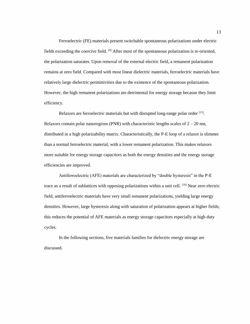
Figure 2-5: The characteristic polarization-electric field hysteresis loops for (a) linear
dielectrics, (b) ferroelectric materials, (c) relaxors, and (d) anti-ferroelectric
materials. The shaded area represents the energy storage densities in each case.
(Modified figure based on Sherrit et al.) .......................................................................... 12
Figure 2-6: The molecular structures of α, β, and γ-phase PVDF. The red balls represent
fluorine atoms, white balls represent hydrogen atoms, and blue balls are carbon
atoms. (Figure adopted from Wan et al.). ........................................................................ 15
Figure 2-7: P-E loops for (a) P(VDF-TrFE) which is ferroelectric and (b) P(VDF-TrFE-
CFE) as a relaxor. The blue areas indicated the energy densities of the two materials.
Figure by B. Chu et al. ..................................................................................................... 16
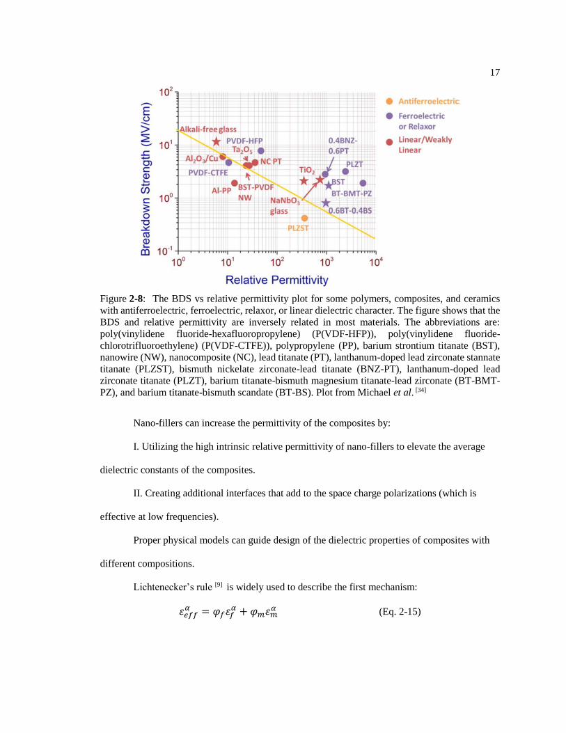
Figure 2-8: The BDS vs relative permittivity plot for some polymers, composites, and
ceramics with antiferroelectric, ferroelectric, relaxor, or linear dielectric character.
The figure shows that the BDS and relative permittivity are inversely related in most
materials. The abbreviations are: poly(vinylidene fluoride-hexafluoropropylene)
(P(VDF-HFP)), poly(vinylidene fluoride- chlorotrifluoroethylene) (P(VDF-CTFE)),
polypropylene (PP), barium strontium titanate (BST), nanowire (NW),
nanocomposite (NC), lead titanate (PT), lanthanum-doped lead zirconate stannate
titanate (PLZST), bismuth nickelate zirconate-lead titanate (BNZ-PT), lanthanum-
doped lead zirconate titanate (PLZT), barium titanate-bismuth magnesium titanate-
lead zirconate (BT-BMT-PZ), and barium titanate-bismuth scandate (BT-BS). Plot
from Michael et al. ........................................................................................................... 17
ix
Figure 2-9: The variation of the effective permittivity of composites with respect to the
volume fraction of high permittivity filler, predicted by multiple models including
parallel connection, series connection, Lichtenecker’s logarithmic law, modified
Lichtenecker’s law, Maxwell-Garnett equation, Bruggeman’s model, Knott
equation, and Yamanda’s model. Figure from Zhang et al. ............................................. 18
Figure 2-10: The multi-core model for polymer-based nanocomposites interfaces
developed by Tanaka et al................................................................................................ 19
Figure 2-11: (a) Some possible geometrical arrangements of various-shaped nano-fillers
(BaTiO3) in an amorphous matrix (PVDF) and (b) their corresponding BDS
estimated by phase field simulations. Figure by Shen et al. ............................................ 20
Figure 2-12: (a) The P-E loops of P(VDF-HFP), OA-10G glass, polyimide, and
polypropylene (PP). (b) The dependence of energy storage densities with respect to
temperatures for the above 4 materials. Plots are originally from Manoharan et al. ....... 21
Figure 2-13: The energy density-relative permittivity relationship of some recently
proposed bulk ceramics. Numbers on the figure represent: (1) Mn-doped 0.8CaTiO3-
0.2CaHfO3 (2) BaTiO3/0.65Bi2O3-0.2B2O3-0.15SiO2 ceramic glass (3)
(Na0.5Bi0.5)TiO3-0.4(Sr0.7Bi0.2)TiO3 (4) 0.7BaTiO3-0.3BiScO3 (5) CaZr0.8Ti0.2O3 (6)
AgNb0.85Ta0.15O3 (7) 0.9(K0.5Na0.5)NbO3-0.1Bi(Mg2/3Nb1/3)O3 (8) AgNbO3 (9)
(Na0.5Bi0.5)0.8Ba0.2Ti0.8Sn0.2O3 (10) BaTiO3-Bi(Zn0.5Ti0.5)O3 (11) 0.92BaTiO3-
0.08K0.73Bi0.09NbO3 (12) 0.9Bi0.48La0.02Na0.48Li0.02Ti0.98Zr0.02O3-0.1Na0.73Bi0.09NbO3
(13) 0.5(SrTiO3)-0.5(0.94Bi0.54Na0.46TiO3-0.06BaTiO3) (14) 0.5SrTiO3-
0.5(0.95Bi0.5Na0.5TiO3-0.05BaAl0.5Nb0.5O3) (15) Bi0.5K0.5TiO3-0.06La(Mg0.5Ti0.5)O3
(16) 0.8BaTiO3-0.2Bi(Mg2/3Nb1/3)O3 (17) 0.695Bi0.5Na0.5TiO3-0.3Sr0.7Bi0.2TiO3-
0.005LaTi0.5Mg0.5O3 (18) CuO-doped BaTiO3-SiO2 ceramic-glass (19)
Ba0.997Sm0.002Zr0.15Ti0.85O3 (20) 0.8BaTiO3-0.2BiYO3 (21) Sr0.92(Bi,Li)0.08TiO3. ............. 23
Figure 2-14: (a) The Cole-Cole plot of Bi1.5Zn0.9Nb1.35Ta0.15O6.9 (BZNT) at different
temperatures. (b) The extrapolated electrical conductivities of BZNT grain interiors
and grain boundaries from (a). Figure by Michael et al. .................................................. 24
Figure 2-15: (a)-(d) Cross-sections showing the microstructure evolution of ceramic Sr1-
x(Bi,Li)xTiO3 (SBLT) with x=0, 0.02, 0.04, and 0.08 respectively. (e) The
corresponding electrical BDS and energy densities of SBLT ceramics. Reproduced
from Alkathy et al. ........................................................................................................... 24
Figure 2-16: TEM of SiO2-coated BaTiO3 nanoparticles when the SiO2 content is (a) 0
wt%, (b) 1.0 wt%, (c) 1.5 wt%, (d) 2.0 wt%, (e) 2.5 wt%, (f) 3.0 wt%, (g) 4.0 wt%,
(h) 6.0 wt% and (i) 8.0 wt%. Figure from Zhang et al. .................................................... 26
Figure 2-17: (a) The P-E loops of AgNbO3 and 15 mol% Ta5+-doped AgNbO3. The
shaded areas indicate the recoverable energy densities. (b) The recoverable energy
storage densities (Wrec) and corresponding energy storage efficiencies of AgNbO3
with dependence of Ta doping levels. (Figure from Zhao et al. ...................................... 27
x
Figure 2-18: Chemical solution deposition process of BNO thin films. DUV denotes deep
UV exposure. ................................................................................................................... 31
Figure 2-19: XRD of BNO thin films with and without UV treatment, and annealed at
different temperatures after spin casting. Unless specifically mentioned in the figure,
the 2nd step heat treatment time was 10 min. Substrate peaks are marked by “*”.
Curves are offset vertically for clarity. ............................................................................ 34
Figure 2-20: (a) The dielectric permittivity and loss tangent as a function of frequency for
BNO films annealed at 350 °C, 375 °C and 400 °C without UV treatment. The
thicknesses of the films are 140 nm, 140 nm and 120 nm respectively. (b) The 10
kHz P-E loops of BNO thin films annealed at 350 °C, 375 °C and 400 °C without
UV treatment. ................................................................................................................... 35
Figure 2-21: (a) Overlay of the carbon XPS depth profiles of BNO thin films annealed at
350 °C with and without UV treatment. (b) The SIMS depth profiles of the BNO
thin films treated without UV exposure and annealed at 350 °C. (c) The SIMS depth
profiles of the BNO thin films treated with UV exposure and annealed at 350 °C. ........ 36
Figure 2-22: The top-down FESEM images of BNO thin films (a) annealed at 450 °C
without UV treatment and (b) annealed at 450 °C with the UV treatment procedure. .... 38
Figure 2-23: (a) The dielectric constants and loss tangent of UV treated BNO thin films
as a function of frequency. (b) The DC leakage currents of BNO thin films with and
without DUV exposure. (c) The P-E loops of UV treated BNO thin films at 10 kHz. .... 40
Figure 2-24: (a) The 10 kHz energy densities and efficiencies of the UV treated BNO thin
films measured under different temperatures at 1 MV/cm. (b) The 1 kHz energy
densities and efficiencies of the UV treated BNO thin films measured at different
temperatures at 1 MV/cm. ................................................................................................ 43
Figure 2-25: Comparison of reported dielectric energy densities for materials processed at
different temperatures. The open symbols are materials with efficiency > 90%.
Notice that the frequencies under which the energy densities and efficiencies were
measured are not uniform. The numbers correspond to materials listed in Table A-1. ... 44
Figure 3-1: The 6 pathways for diffusion between ceramic particles: 1. Surface diffusion.
2. Lattice diffusion from the surface. 3. Vapor transport. 4. Grain boundary
diffusion. 5. Lattice diffusion from the grain boundary. 6. Plastic flow. (Picture from
Rahaman et al. (2003).) .................................................................................................... 58
Figure 3-2: Illustration of morphology change in ceramic grains (a) before sintering, (b)
at the initial stage of sintering when necks begin to form, (c) during the intermediate
stage of sintering when grains turn into tetrakaidecahedrons with inter-connected
pores, and (d) at final stage during which the channels along the grain edge close up
and pores are isolated. (Figure adopted from Coble et al. (1961).) ................................. 60
xi
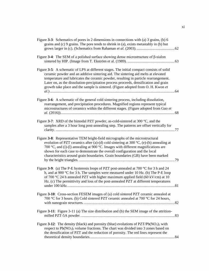
Figure 3-3: Schematics of pores in 2 dimensions in connections with (a) 3 grains, (b) 6
grains and (c) 9 grains. The pore tends to shrink in (a), exists metastably in (b) but
grows larger in (c). (Schematics from Rahaman et al. (2003). ........................................ 62
Figure 3-4: The SEM of a polished surface showing dense microstructure of β-sialon
sintered by HIP. (Image from T. Ekström et al. (1989). .................................................. 63
Figure 3-5: A schematic of LPS at different stages. The initial compact consists of solid
ceramic powder and an additive sintering aid. The sintering aid melts at elevated
temperature and lubricates the ceramic powder, resulting in particle rearrangement.
Later on, as the dissolution-precipitation process proceeds, densification and grain
growth take place and the sample is sintered. (Figure adopted from O. H. Kwon et
al.) .................................................................................................................................... 64
Figure 3-6: A schematic of the general cold sintering process, including dissolution,
rearrangement, and precipitation procedures. Magnified regions represent typical
microstructures of ceramics within the different stages. (Figure adopted from Guo et
al. (2016))......................................................................................................................... 68
Figure 3-7: XRD of the bimodal PZT powder, as-cold-sintered at 300 °C, and the
samples after a 3 hour long post-annealing step. The patterns are offset vertically for
clarity. .............................................................................................................................. 77
Figure 3-8: Representative TEM bright-field micrographs of the microstructural
evolution of PZT ceramics after (a)-(d) cold sintering at 300 °C, (e)-(h) annealing at
700 °C, and (i)-(l) annealing at 900 °C. Images with different magnifications are
shown for each case to demonstrate the overall configuration and the local
characteristics around grain boundaries. Grain boundaries (GB) have been marked
by the bright triangles. ..................................................................................................... 79
Figure 3-9: (a) The P-E hysteresis loops of PZT post-annealed at 700 °C for 3 h and 24
h, and at 900 °C for 3 h. The samples were measured under 10 Hz. (b) The P-E loop
of 700 °C 24 h annealed PZT with higher maximum applied field (60 kV/cm) at 10
Hz. (c) The permittivity and loss of the post-annealed PZT at different temperatures
under 100 kHz. ................................................................................................................. 81
Figure 3-10: Cross-section FESEM images of (a) cold sintered PZT ceramic annealed at
700 °C for 3 hours. (b) Cold sintered PZT ceramic annealed at 700 °C for 24 hours,
with nanograin structures. ................................................................................................ 82
Figure 3-11: Figure 3-11 (a) The size distribution and (b) the SEM image of the attrition-
milled PZT-5A powder. ................................................................................................... 83
Figure 3-12: The density (black) and porosity (blue) evolutions of PZT/Pb(NO3)2 with
respect to Pb(NO3)2 volume fractions. The chart was divided into 3 zones based on
the densification of PZT and the reduction of porosity. The red lines represent the
theoretical density boundaries. ......................................................................................... 84
xii
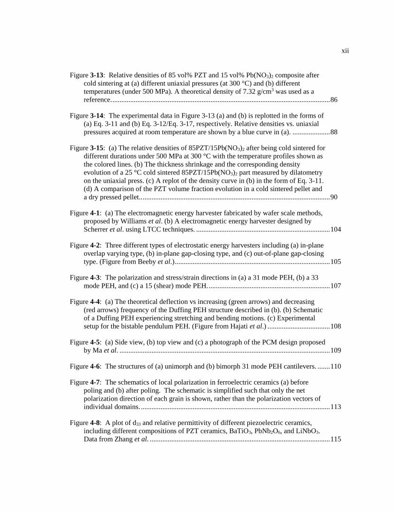
Figure 3-13: Relative densities of 85 vol% PZT and 15 vol% Pb(NO3)2 composite after
cold sintering at (a) different uniaxial pressures (at 300 °C) and (b) different
temperatures (under 500 MPa). A theoretical density of 7.32 g/cm3 was used as a
reference. .......................................................................................................................... 86
Figure 3-14: The experimental data in Figure 3-13 (a) and (b) is replotted in the forms of
(a) Eq. 3-11 and (b) Eq. 3-12/Eq. 3-17, respectively. Relative densities vs. uniaxial
pressures acquired at room temperature are shown by a blue curve in (a). ..................... 88
Figure 3-15: (a) The relative densities of 85PZT/15Pb(NO3)2 after being cold sintered for
different durations under 500 MPa at 300 °C with the temperature profiles shown as
the colored lines. (b) The thickness shrinkage and the corresponding density
evolution of a 25 °C cold sintered 85PZT/15Pb(NO3)2 part measured by dilatometry
on the uniaxial press. (c) A replot of the density curve in (b) in the form of Eq. 3-11.
(d) A comparison of the PZT volume fraction evolution in a cold sintered pellet and
a dry pressed pellet.. ......................................................................................................... 90
Figure 4-1: (a) The electromagnetic energy harvester fabricated by wafer scale methods,
proposed by Williams et al. (b) A electromagnetic energy harvester designed by
Scherrer et al. using LTCC techniques. ........................................................................... 104
Figure 4-2: Three different types of electrostatic energy harvesters including (a) in-plane
overlap varying type, (b) in-plane gap-closing type, and (c) out-of-plane gap-closing
type. (Figure from Beeby et al.) ....................................................................................... 105
Figure 4-3: The polarization and stress/strain directions in (a) a 31 mode PEH, (b) a 33
mode PEH, and (c) a 15 (shear) mode PEH. .................................................................... 107
Figure 4-4: (a) The theoretical deflection vs increasing (green arrows) and decreasing
(red arrows) frequency of the Duffing PEH structure described in (b). (b) Schematic
of a Duffing PEH experiencing stretching and bending motions. (c) Experimental
setup for the bistable pendulum PEH. (Figure from Hajati et al.) ................................... 108
Figure 4-5: (a) Side view, (b) top view and (c) a photograph of the PCM design proposed
by Ma et al. ...................................................................................................................... 109
Figure 4-6: The structures of (a) unimorph and (b) bimorph 31 mode PEH cantilevers. ....... 110
Figure 4-7: The schematics of local polarization in ferroelectric ceramics (a) before
poling and (b) after poling. The schematic is simplified such that only the net
polarization direction of each grain is shown, rather than the polarization vectors of
individual domains. .......................................................................................................... 113
Figure 4-8: A plot of d33 and relative permittivity of different piezoelectric ceramics,
including different compositions of PZT ceramics, BaTiO3, PbNb2O6, and LiNbO3.
Data from Zhang et al. ..................................................................................................... 115
xiii
Figure 4-9: (a) Photos of curved PZT plates attached to 3D printed PET frames. (b) The
device configuration of “gullwing”-structured PEH excited by a rotating gear. Figure
by Yang et al. ................................................................................................................... 116
Figure 4-10: SEM showing (a) the microstructure and (b) micro-cracks on 5.4 µm thick
PZT thin films. Images from Yeo et al. ........................................................................... 118
Figure 4-11: Schematic flow chart for the fabrication of PZT/metal/PZT 2-2 composites.
The photograph on the bottom left shows a PZT thick film on Ni foil after post-
sintering. ........................................................................................................................... 121
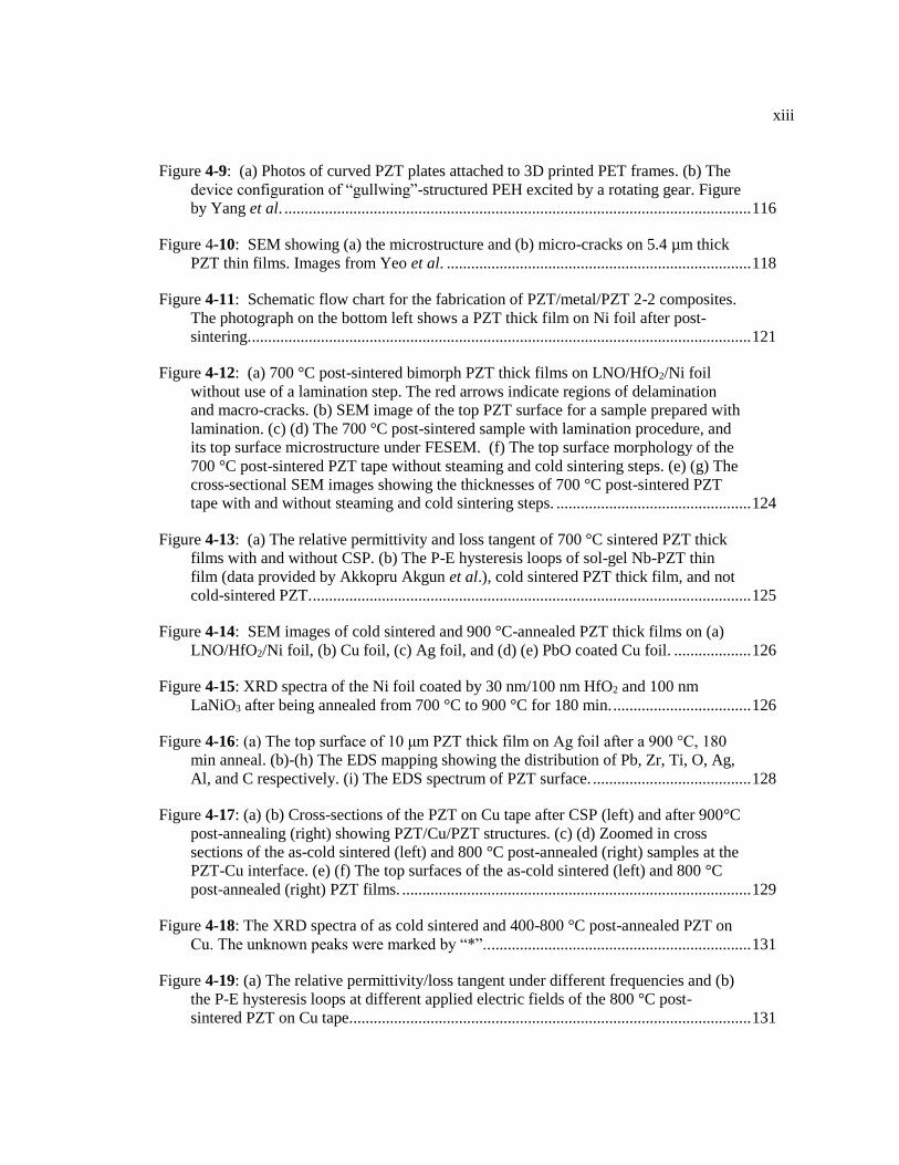
Figure 4-12: (a) 700 °C post-sintered bimorph PZT thick films on LNO/HfO2/Ni foil
without use of a lamination step. The red arrows indicate regions of delamination
and macro-cracks. (b) SEM image of the top PZT surface for a sample prepared with
lamination. (c) (d) The 700 °C post-sintered sample with lamination procedure, and
its top surface microstructure under FESEM. (f) The top surface morphology of the
700 °C post-sintered PZT tape without steaming and cold sintering steps. (e) (g) The
cross-sectional SEM images showing the thicknesses of 700 °C post-sintered PZT
tape with and without steaming and cold sintering steps. ................................................ 124
Figure 4-13: (a) The relative permittivity and loss tangent of 700 °C sintered PZT thick
films with and without CSP. (b) The P-E hysteresis loops of sol-gel Nb-PZT thin
film (data provided by Akkopru Akgun et al.), cold sintered PZT thick film, and not
cold-sintered PZT. ............................................................................................................ 125
Figure 4-14: SEM images of cold sintered and 900 °C-annealed PZT thick films on (a)
LNO/HfO2/Ni foil, (b) Cu foil, (c) Ag foil, and (d) (e) PbO coated Cu foil. ................... 126
Figure 4-15: XRD spectra of the Ni foil coated by 30 nm/100 nm HfO2 and 100 nm
LaNiO3 after being annealed from 700 °C to 900 °C for 180 min. .................................. 126
Figure 4-16: (a) The top surface of 10 μm PZT thick film on Ag foil after a 900 °C, 180
min anneal. (b)-(h) The EDS mapping showing the distribution of Pb, Zr, Ti, O, Ag,
Al, and C respectively. (i) The EDS spectrum of PZT surface. ....................................... 128
Figure 4-17: (a) (b) Cross-sections of the PZT on Cu tape after CSP (left) and after 900°C
post-annealing (right) showing PZT/Cu/PZT structures. (c) (d) Zoomed in cross
sections of the as-cold sintered (left) and 800 °C post-annealed (right) samples at the
PZT-Cu interface. (e) (f) The top surfaces of the as-cold sintered (left) and 800 °C
post-annealed (right) PZT films. ...................................................................................... 129
Figure 4-18: The XRD spectra of as cold sintered and 400-800 °C post-annealed PZT on
Cu. The unknown peaks were marked by “*”.. ................................................................ 131
Figure 4-19: (a) The relative permittivity/loss tangent under different frequencies and (b)
the P-E hysteresis loops at different applied electric fields of the 800 °C post-
sintered PZT on Cu tape. .................................................................................................. 131
xiv
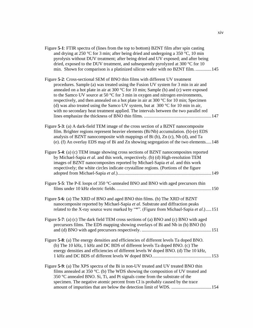
Figure 5-1: FTIR spectra of (lines from the top to bottom) BZNT film after spin casting
and drying at 250 °C for 3 min; after being dried and undergoing a 350 °C, 10 min
pyrolysis without DUV treatment; after being dried and UV exposed; and after being
dried, exposed to the DUV treatment, and subsequently pyrolyzed at 300 °C for 10
min. Shown for comparison is a platinized silicon wafer with no BZNT film. .............. 145
Figure 5-2: Cross-sectional SEM of BNO thin films with different UV treatment
procedures. Sample (a) was treated using the Fusion UV system for 3 min in air and
annealed on a hot plate in air at 300 °C for 10 min; Sample (b) and (c) were exposed
to the Samco UV source at 50 °C for 3 min in oxygen and nitrogen environments,
respectively, and then annealed on a hot plate in air at 300 °C for 10 min; Specimen
(d) was also treated using the Samco UV system, but at 300 °C for 10 min in air,
with no secondary heat treatment applied. The intervals between the two parallel red
lines emphasize the thickness of BNO thin films. ........................................................... 147
Figure 5-3: (a) A dark-field TEM image of the cross section of a BZNT nanocomposite
film. Brighter regions represent heavier elements (Bi/Nb) accumulation. (b)-(e) EDS
analysis of BZNT nanocomposite with mappings of Bi (b), Zn (c), Nb (d), and Ta
(e). (f) An overlay EDS map of Bi and Zn showing segregation of the two elements..... 148
Figure 5-4: (a) (c) TEM image showing cross sections of BZNT nanocomposites reported
by Michael-Sapia et al. and this work, respectively. (b) (d) High-resolution TEM
images of BZNT nanocomposites reported by Michael-Sapia et al. and this work
respectively; the white circles indicate crystalline regions. (Portions of the figure
adopted from Michael-Sapia et al.) .................................................................................. 149
Figure 5-5: The P-E loops of 350 °C-annealed BNO and BNO with aged precursors thin
films under 10 kHz electric fields. ................................................................................... 150
Figure 5-6: (a) The XRD of BNO and aged BNO thin films. (b) The XRD of BZNT
nanocomposite reported by Michael-Sapia et al. Substrate and diffraction peaks
related to the X-ray source were marked by “*”. (Figure from Michael-Sapia et al.) ..... 151
Figure 5-7: (a) (c) The dark field TEM cross sections of (a) BNO and (c) BNO with aged
precursors films. The EDS mapping showing overlays of Bi and Nb in (b) BNO (b)
and (d) BNO with aged precursors respectively. ............................................................. 151
Figure 5-8: (a) The energy densities and efficiencies of different levels Ta doped BNO.
(b) The 10 kHz, 1 kHz and DC BDS of different levels Ta doped BNO. (c) The
energy densities and efficiencies of different levels W doped BNO. (d) The 10 kHz,
1 kHz and DC BDS of different levels W doped BNO. ................................................... 153
Figure 5-9: (a) The XPS spectra of the Bi in non-UV treated and UV treated BNO thin
films annealed at 350 °C. (b) The WDS showing the composition of UV treated and
350 °C annealed BNO. Si, Ti, and Pt signals come from the substrate of the
specimen. The negative atomic percent from Cl is probably caused by the trace
amount of impurities that are below the detection limit of WDS. ................................... 154
xv
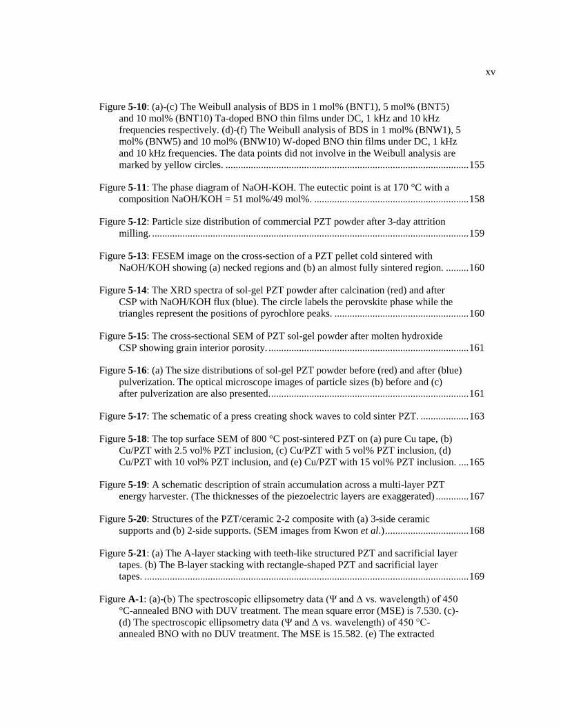
Figure 5-10: (a)-(c) The Weibull analysis of BDS in 1 mol% (BNT1), 5 mol% (BNT5)
and 10 mol% (BNT10) Ta-doped BNO thin films under DC, 1 kHz and 10 kHz
frequencies respectively. (d)-(f) The Weibull analysis of BDS in 1 mol% (BNW1), 5
mol% (BNW5) and 10 mol% (BNW10) W-doped BNO thin films under DC, 1 kHz
and 10 kHz frequencies. The data points did not involve in the Weibull analysis are
marked by yellow circles. ................................................................................................ 155
Figure 5-11: The phase diagram of NaOH-KOH. The eutectic point is at 170 °C with a
composition NaOH/KOH = 51 mol%/49 mol%. ............................................................. 158
Figure 5-12: Particle size distribution of commercial PZT powder after 3-day attrition
milling. ............................................................................................................................. 159
Figure 5-13: FESEM image on the cross-section of a PZT pellet cold sintered with
NaOH/KOH showing (a) necked regions and (b) an almost fully sintered region. ......... 160
Figure 5-14: The XRD spectra of sol-gel PZT powder after calcination (red) and after
CSP with NaOH/KOH flux (blue). The circle labels the perovskite phase while the
triangles represent the positions of pyrochlore peaks. ..................................................... 160
Figure 5-15: The cross-sectional SEM of PZT sol-gel powder after molten hydroxide
CSP showing grain interior porosity. ............................................................................... 161
Figure 5-16: (a) The size distributions of sol-gel PZT powder before (red) and after (blue)
pulverization. The optical microscope images of particle sizes (b) before and (c)
after pulverization are also presented. .............................................................................. 161
Figure 5-17: The schematic of a press creating shock waves to cold sinter PZT. ................... 163
Figure 5-18: The top surface SEM of 800 °C post-sintered PZT on (a) pure Cu tape, (b)
Cu/PZT with 2.5 vol% PZT inclusion, (c) Cu/PZT with 5 vol% PZT inclusion, (d)
Cu/PZT with 10 vol% PZT inclusion, and (e) Cu/PZT with 15 vol% PZT inclusion. .... 165
Figure 5-19: A schematic description of strain accumulation across a multi-layer PZT
energy harvester. (The thicknesses of the piezoelectric layers are exaggerated) ............. 167
Figure 5-20: Structures of the PZT/ceramic 2-2 composite with (a) 3-side ceramic
supports and (b) 2-side supports. (SEM images from Kwon et al.) ................................. 168
Figure 5-21: (a) The A-layer stacking with teeth-like structured PZT and sacrificial layer
tapes. (b) The B-layer stacking with rectangle-shaped PZT and sacrificial layer
tapes. ................................................................................................................................ 169
Figure A-1: (a)-(b) The spectroscopic ellipsometry data (Ψ and Δ vs. wavelength) of 450
°C-annealed BNO with DUV treatment. The mean square error (MSE) is 7.530. (c)-
(d) The spectroscopic ellipsometry data (Ψ and Δ vs. wavelength) of 450 °C-
annealed BNO with no DUV treatment. The MSE is 15.582. (e) The extracted
xvi
refractive index vs. wavelength for 450 °C-annealed BNO thin films with and
without UV exposure. ...................................................................................................... 176
Figure A-2: (a) The 1 kHz energy densities and efficiencies of the UV treated BNO thin
films measured under different temperatures at their maximum electric fields. (b)
The 10 kHz energy densities and efficiencies of the UV treated BNO thin films
measured at different temperatures at their maximum electric fields. ............................. 177
Figure B-1: (a) Representative HAADF micrograph, (b)-(e) corresponding EDS chemical
mapping, and (f) EDS spectrum, of the PZT ceramics cold sintered at 300 ºC. .............. 181
Figure B-2: (a) Representative HAADF micrograph, (b)-(e) corresponding EDS chemical
mapping, and (f) EDS spectrum, of the cold sintered PZT ceramics after annealing at
700 ºC. .............................................................................................................................. 182
Figure B-3: (a) Representative HAADF micrograph, (b)-(e) corresponding EDS chemical
map, and (f) EDS spectrum of the cold sintered PZT ceramics after annealing at 900
ºC. ..................................................................................................................................... 182
Figure B-4: (a) FESEM fracture surface image of a bimodal PZT pellet uniaxially pressed
without cold sintering (e.g. no lead nitrate or liquid at 300 ºC for 3 hrs) under 500
MPa and post-annealed at 900 ºC for 3 hrs in air. (b) The bimodal PZT cold sintered
with lead nitrate sintering aid at 300 ºC for 3 hrs under 500 MPa and post-annealed
at 900 ºC for 3 hrs in air. .................................................................................................. 183
Figure C-1: (a) The surface morphology of an 800 °C annealed PZT tape without lead
nitrate as a sintering aid. .................................................................................................. 184
Figure C-2: (a) The top surface of 800 °C annealed PZT indicating a Cu2O crystal. (b)-(g)
EDS mapping of Cu, O, Pb, Zr, Ti, and C respectively. (h) The EDS spectrum of
PZT surface. ..................................................................................................................... 185
Figure C-3: The XRD spectra of 800 °C post-sintered PZT on Cu with Cu2O
contamination (Process A), the 800 °C post-sintered PZT on Cu from PZT tape
without lead nitrate (Process B), and the sintered PZT/Cu composite using a cleaned
(at 900 °C for 12 hours) alumina sample holder (Process C). .......................................... 186
Figure C-4: (a) (b) Cross-sectional SEM of as cold-sintered PZT/Cu (left) and 800 °C
annealed PZT/Cu (right) showing the EDS line scan positions. (c) (d) The EDS line
scans of the two above regions. (e) (f) The EDS spectra from the line scans on as
cold-sintered PZT/Cu (left) and 800 °C annealed PZT/Cu (right). .................................. 187
Figure C-5: (a) Cross-sectional and (b) top-down SEM of cold sintered and 400 °C 3hrs
annealed PZT/Cu. (c) (d) Cross-sectional and top-down SEM of cold sintered and
500 °C 3hrs annealed PZT/Cu. (e) (f) SEM of cold sintered and 600 °C 3hrs
annealed PZT/Cu. (g) (h) SEM of cold sintered and 700 °C 3hrs annealed PZT/Cu. ..... 188
xvii
LIST OF TABLES
Table 2-1: The FWHM values for the BNO thin films. ........................................................... 39
Table 2-2: The average DC breakdown strengths of the BNO thin films with 95% CI.
Five electrodes were tested to allow an average value to be calculated. .......................... 41
Table 2-3: The maximum energy storage densities and the efficiencies of BNO thin films
prepared using the UV treatment. .................................................................................... 41
Table 2-4: The maximum energy storage densities and the efficiencies of the DUV
treated BNO thin films with efficiencies ≥ 90%. ............................................................. 42
Table 3-1: Some typical materials that have been cold sintered. The cold sintering
conditions and their potential applications are also listed. ............................................... 70
Table 3-2: The densities and d33 of cold sintered (300 ˚C, 500 MPa, 3 hrs) PZT with
different post-annealing temperatures. The d33 values are the average of 3
measurements of the same sample for each condition. .................................................... 76
Table 4-1: Comparisons of piezoelectric coefficients (d33) between single crystals and
ceramics. .......................................................................................................................... 113
Table 5-1: UV treatment conditions and electrical properties of BNO thin films. ................. 146
Table 5-2: Sintering techniques categorized by forms of energy input. ................................. 162
Table A-1: A summary of the additional information on the materials mentioned in
Figure 2-25 including maximum processing temperatures, energy densities,
maximum applied fields, efficiencies, frequencies, sample thicknesses, electrode
materials and electrode diameters. The numbers in the table correspond to the
numbers in Figure 2-25. ................................................................................................... 178
xviii
ACKNOWLEDGEMENTS
Even many years later, as I will probably still keep striving for my ambition somewhere,
I shall never forget that distant summer afternoon when I first landed in State College, the willow
was gently fiddled by the wind. Now, Nittany Mountain is hibernating amongst the cold rain, and
the finale of my student era is near. This is the seventh year of me being a “Penn Stater”.
Although it is never possible to list every person I have received help from in the past seven
years, a few of them must be addressed for their importance in my life.
First and foremost, I would like to present my greatest appreciation to Dr. Susan Trolier-
McKinstry. She is not only a knowledgeable advisor with inspiring ideas, excellent teaching
skills, and brilliant problem-solving techniques, but also an educator of merits to be admired.
After an intensive four-and-half-year PhD program, I have been taught to love my career, stay
humble, be suspicious as a scientist, and always shoot for perfection.
I would also acknowledge my thesis committee members: Dr. Clive Randall, Dr. Tom
Jackson, and Dr. Qing Wang. They have led me to many helpful discussions to strengthen my
weak points during the comprehensive exam, as well as providing suggestions for my project
from their expertise.
I would like to thank the staff members in MSC, including Beth Jones, Amanda Baker,
Bangzhi Liu, Bill Drawl, Mike Labella, Andy Fitzgerald, Guy Lavallee, Kathy Gehoski, Chad
Eichfeld, Ke Wang, Julie Anderson, Nicole Wonderling, Katya Bazilevskaya, Maria Dicola,
Manuel Villalpando, Gino Tambourine, Jeff Long, Steve Perini, Tim Klinger, and Damina
Richards for their support.
My appreciation should also be shared with the past and current group members of Dr.
Susan Trolier-McKinstry and Dr. Clive Randall: Sandie Elder, Elizabeth Michael, Ryan Keech,
Hong Goo Yeo, Carl Morandi, Wanlin Zhu, Song Won Ko, Jung In Yang, Smitha Shetty,
xix
Veronika Kovacova, Daisuke Hama, Sanshiro Aman, Lyndsey Dennis, Trent Borman, Betul
Akkopru Akgun, Tianning Liu, Kathleen Coleman, Chris Cheng, Leonard Jacques, Nicole Hall,
Shruti Gupta, Nathan Bishop, Mike Hahn, Travis Peters, Pannawit Tipsawat, Joanne Aller,
Hanzheng Guo, Jing Guo, Lisheng Gao, Seth Berbano, Sinan Dursun, Arnaud Nadayishimiye,
Kosuke Tsuji, Joo Hwan Seo, Sun Hwi Bang, and Zane Grady.
This thesis would never be completed without the help from all the collaborators, and I
give thanks to Dr. Shad Roundy, Dr. Mehdi Kiani, Binh Duc Truong, Miao Meng, Mike Clark,
and Tony Sokolov. I would also like to acknowledge the Dow Chemical Company and Empower
Materials, Inc. for their supplies.
A group of friends Yihuang Xiong, Kehao Zhang, Jinwen Zhu, Chengye Dong, Ding Ai,
Wenbo Guo, Ying Zhang, Weinan Chen, Zhuqing Wang, Ning Yi, and Xiaotian Zhang, and Siyu
Xu should be acknowledged for all the interdisciplinary discussions during our weekly “Hot Pot
Seminar.” Some really interesting ideas engendered during these discussions are reflected in the
future work of this thesis.
I have to mention two of my previous advisors: Dr. Joshua Robinson and Dr. Yaming
Wang (Harbin Institute of Technology, China). The experiences working in their groups have
solidified the foundation of my research and have brought me a broad vision.
Financial support for this thesis was provided by Dow Chemical and NSF ASSIST
funding.
Last but not the least, I would give a special thanks to my parents Baojin Wang and Li
Cai, and my family for their love and care.
Chapter 1
Statement of Goals and Thesis Organization
1.1 Statement of purpose
The rapidly growing market of wearable and implantable electronics has brought
convenience to people’s lives as well as challenges to material scientists: How to advance the
material synthesis and processing techniques that suits the fabrication of those devices. In
particular, there is a need to develop flexible, miniaturized, non-toxic, and high-performance
material systems. Especially for electro-ceramics, the synthesis and processing of which are
generally carried out at temperatures too high for most flexible organic and metallic substrates,
technology upgrades are essential.
As an example, the deposition of oxide thin films by either chemical solution deposition
or physical/chemical vapor deposition, requires minimum crystallization temperatures typically
above 600 °C, where almost all polymers will be immediately pyrolyzed, and base metals are
subject to oxidation. Lowering the deposition temperatures, however, induces degraded
crystallinity, secondary phases, or chemical residues that diminish the energy storage densities of
the products. A low temperature deposition process should be proposed along with novel material
systems to maximize the energy storage performance.
Another important trend for future implantable electronics is self-powering, since many
devices are expected to provide continuous service. Currently developed self-power solutions
based on piezoelectric energy harvesters have limited power density and low energy conversion
2
efficiencies due to constraints on piezoelectric layer thickness. Thicker piezoelectric layers
deposited by sol-gel or sputtering method are not only expensive but also present high micro-
crack densities. And ceramic thick films prepared by low temperature co-fired ceramic (LTCC)
technologies are typically difficult to densify. Cold sintering has the potential to densify ceramic
pellets and thick films at an acceptably low temperature range, and might be useful for
manufacturing high figure of merit piezoelectric energy harvester beams.
1.2 Dissertation structure
The thesis was constructed with three main topics focusing on the processing of ceramic
thin films, pellets, and thick films at temperatures lower than conventional techniques.
Chapter 2 discusses the development of bismuth-based thin film energy storage
capacitors. Facilitated by deep ultra-violet (DUV) treatment, bismuth niobate thin films with
improved electrical properties were achieved. The influences of DUV radiation on density,
crystallinity, relative permittivity, and electric breakdown strength were compared under different
heat treatment temperatures. Future work also suggested some preliminary results for the further
increase in the energy densities.
Chapter 3 depicts an exploration on the cold sintering process of bulk lead zirconate
titanate (PZT) ceramics. The microstructure, dielectric properties, and piezoelectric constants of
PZT powder cold sintered with moistened lead nitrate are presented. The underlying densification
mechanisms of PZT as well as the effects of cold sintering temperature, pressure, and holding
time were incorporated into a modified viscous sintering model. A one-step sintering technique is
introduced at the end of this chapter that can potentially fully densify PZT below 400 °C.
Chapter 4 describes the attempt to cold sinter PZT thick films with metal for high voltage
piezoelectric energy harvesters. With the pathways paved by the studies on pellet cold sintering,

3
this process was successfully integrated with tape cast piezoelectric layers. The behaviors of PZT
along with multiple commonly used metals during cold sintering and post-sintering was
evaluated.
* Part of this chapter is reproduced from D. Wang, M. Clark, and S. Trolier-McKinstry “Bismuth
Niobate Thin Films for Dielectric Energy Storage Applications.” Journal of the American
Ceramic Society 101 (8), 3343-3451 (2018).
Chapter 2
Ultra-Violet-Assisted Low Temperature Processing of Bismuth Niobate Thin
Film for Dielectric Energy Storage Capacitors
2.1 Introduction
Capacitive energy storage is of interest for high charge-discharge rates in electronic
circuits. With the rapid development of wearable electronic devices, flexible electronics, and
embedded passive components, integration of capacitors on polymer films [1–3] or metal foils [4,5]
has drawn recent interest. Moreover, the miniaturization of microelectronic devices requires
materials with high volumetric energy storage densities. Thus, there is interest in developing new
materials and processes for high energy storage density capacitors on flexible substrates. Many
widely studied oxide thin films, such as BaTiO3 [6] and Bi1.5ZnNb1.5O7 [7], are suitable for dielectric
energy storage, but require high crystallization temperatures beyond the glass transition
temperatures of polymers, and annealing atmospheres that oxidize base metal foils.
This work explores low temperature processed Bi3NbO7 (BNO) thin films as potential
candidates for high energy density capacitors. The BNO samples were fabricated by a chemical
solution deposition method followed by ultra-violet (UV) exposure and heat treatments. A UV
treatment prior to the final pyrolysis step was found to eliminate bound carbon and promote
crystallization of BNO at low temperatures. Following a series of heat treatments from 350 °C -
450 °C, the energy storage density of the BNO thin film increased from 13 J/cm3 to 39 J/cm3.
Furthermore, 350 °C and 375 °C treated BNO samples showed that the efficiencies of the films
remained above 97% up to 150 °C at 10 kHz under 1 MV/cm applied field.
5
2.2 Literature review
2.2.1 Dielectric energy storage capacitors
A capacitor is a device that stores electrical energy. Compared with batteries and fuel
cells, capacitors have low to modest levels of specific energy (or energy densities) but very high
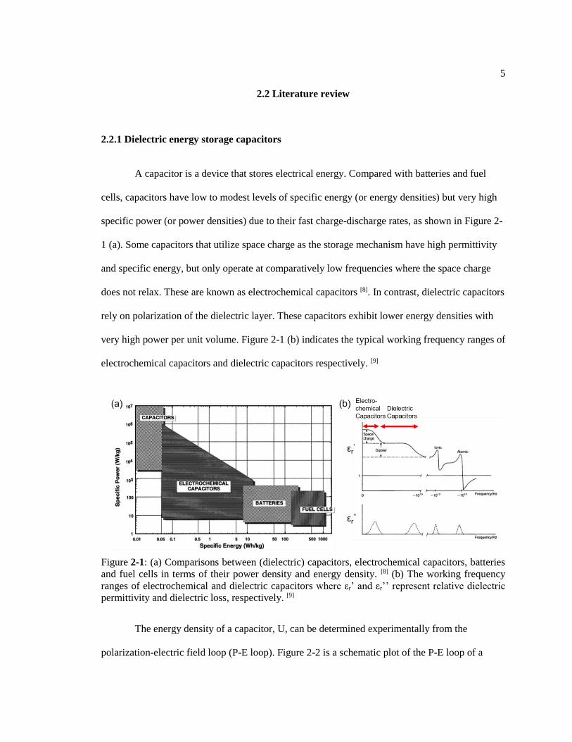
specific power (or power densities) due to their fast charge-discharge rates, as shown in Figure 2-
1 (a). Some capacitors that utilize space charge as the storage mechanism have high permittivity
and specific energy, but only operate at comparatively low frequencies where the space charge
does not relax. These are known as electrochemical capacitors [8]. In contrast, dielectric capacitors
rely on polarization of the dielectric layer. These capacitors exhibit lower energy densities with
very high power per unit volume. Figure 2-1 (b) indicates the typical working frequency ranges of
electrochemical capacitors and dielectric capacitors respectively. [9]
The energy density of a capacitor, U, can be determined experimentally from the
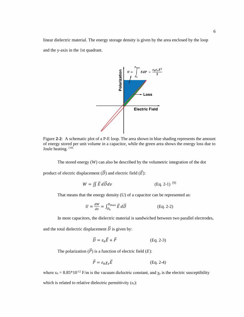
polarization-electric field loop (P-E loop). Figure 2-2 is a schematic plot of the P-E loop of a
Figure 2-1: (a) Comparisons between (dielectric) capacitors, electrochemical capacitors, batteries
and fuel cells in terms of their power density and energy density. [8] (b) The working frequency
ranges of electrochemical and dielectric capacitors where εr’ and εr’’ represent relative dielectric
permittivity and dielectric loss, respectively. [9]
6
linear dielectric material. The energy storage density is given by the area enclosed by the loop
and the y-axis in the 1st quadrant.
The stored energy (W) can also be described by the volumetric integration of the dot
product of electric displacement (�⃗⃗� ) and electric field (�⃗� ):
𝑊 = ∬�⃗� 𝑑�⃗⃗� 𝑑𝑣 (Eq. 2-1) [9]
That means that the energy density (U) of a capacitor can be represented as:
𝑈 =𝑑𝑊
𝑑𝑣= ∫ �⃗�
𝐷𝑚𝑎𝑥
𝐷0𝑑�⃗⃗� (Eq. 2-2)
In most capacitors, the dielectric material is sandwiched between two parallel electrodes,
and the total dielectric displacement �⃗⃗� is given by:
�⃗⃗� = 휀0�⃗� + �⃗� (Eq. 2-3)
The polarization (�⃗� ) is a function of electric field (𝐸):
�⃗� = 휀0𝜒𝑒�⃗� (Eq. 2-4)
where ε0 = 8.85*10-12 F/m is the vacuum dielectric constant, and χe is the electric susceptibility
which is related to relative dielectric permittivity (εr):
Figure 2-2: A schematic plot of a P-E loop. The area shown in blue shading represents the amount
of energy stored per unit volume in a capacitor, while the green area shows the energy loss due to
Joule heating. [10]
7
𝜒𝑒 = 휀𝑟 − 1 (Eq. 2-5)
For many dielectric materials, the relative permittivity is much larger than 1, χe ≈ εr.
Thus:
𝑈 = ∫ �⃗� 𝑃𝑚𝑎𝑥
𝑃0𝑑�⃗� (Eq. 2-6)
For an ideal linear dielectric material with no loss, all the input energy can be stored and
fully extracted upon discharging the capacitor, giving an inclined single line for the P-E loop.
However, in practice, materials have a finite electrical conductivity and part of the input energy is
dissipated via Joule heating. This loss is represented as the green region in Figure 2-2, which has
an area of:
𝑤𝑒 = 2𝜋 ∙ 𝑈 ∙ 𝑡𝑎𝑛𝛿 (Eq. 2-7) [11]
where tanδ is called the loss tangent of a material.
Considering the loss of a capacitor, the energy storage efficiency (η) can be defined as:
𝜂 =𝑈𝑟𝑒𝑐
𝑈𝑡𝑜𝑡𝑎𝑙=
𝑈𝑟𝑒𝑐
𝑈𝑟𝑒𝑐+𝑤𝑒× 100% (Eq. 2-8)
Urec is the recoverable (or discharge) energy density, Utotal is the total energy input during
charging. Figure 2-2 shows that the energy storage efficiency is the fraction of the blue area with
respect to the sum of blue and green areas. During the design of novel energy storage materials, it
is almost as important to consider the energy storage efficiency as the magnitude of recoverable
energy density; less efficient capacitors waste energy, and have shorter lifetimes due to
degradation caused by accumulated Joule heating.
By plugging Eq. 2-3, Eq. 2-4, and Eq. 2-5 into Eq. 2-2, and assuming the electric
displacement is in the same direction as the applied electric field:
𝑈 =1
2휀0휀𝑟𝐸
2 (Eq. 2-9)
8
From Eq. 2-9, it is obvious that in the case of an ideal linear dielectric material with
negligible loss tangent, the energy density is proportional to εr and E2, which means that high
energy storage densities can be achieved in materials with not only large dielectric constants but
also high breakdown strengths (BDS, the highest applicable electric field before short circuiting
the capacitor). And since energy density is proportional to the square of electric field, materials
with modest permittivity but outstanding BDS are more suitable for energy storage in high
voltage systems. Therefore, it is of interest to understand the electrical breakdown mechanisms.
2.2.2 Electrical breakdown mechanisms
The electrical breakdown defines the “failure of dielectrics under electrical stress”. [9]
There are three main mechanisms that contribute to electrical breakdown: intrinsic (avalanche)
breakdown, thermal breakdown, and discharge breakdown.
2.2.2.1 Intrinsic (avalanche) breakdown
Intrinsic breakdown describes the process during which, upon steadily increasing electric
fields, the leakage currents in a sample first saturate, and then increase sharply within 10-8 sec.
The intrinsic breakdown process can be depicted as the electric current amplification due to a
combination of electron injection from the cathode and the collision ionization with the
dielectrics: [12]
𝐽(𝑑) = 𝐽0𝑒𝑥𝑝 [−4(2𝑚)
12𝛷
32
3ℏ𝑒𝐸+
𝑒𝐸𝑑
𝐸𝑎] (Eq. 2-10)
where J is the current density, d is the thickness of the sample, m is the effective mass of the
electrons, Φ is the work function of the cathode, Ea is the material-dependent activation energy
9
for collision ionization, ħ=h/2π represents the reduced Planck’s constant, e is the electron charge,
and E is the applied electric field.
From Eq. 2-10, breakdown should occur when the current density starts to increase and
do damage to the dielectric, namely, when
−4(2𝑚)
12𝛷
32
3ℏ𝑒𝐸+
𝑒𝐸𝑑
𝐸𝑎= 0 (Eq. 2-11)
Solving for E yields:
𝐸𝑏𝑟𝑒𝑎𝑘𝑑𝑜𝑤𝑛 = √4(2𝑚)12𝛷
32𝐸𝑎
3ℏ𝑒2𝑑≈
3×10⁴
𝑑12
𝑉/𝑐𝑚 (Eq. 2-12)
Eq. 2-12 suggests for the same homogeneous material with the same electrodes, the
intrinsic breakdown strength should be inversely proportional to the square root of the dielectric
thickness.
2.2.2.2 Thermal breakdown
Thermal breakdown appears when a device generates heat faster than the heat is
dissipated. The accumulated heat increases the temperature of the dielectric, elevates the ionic
and electronic conductivities, and eventually leads to breakdown. [9] Thermal breakdown behavior
is governed by Eq. (2-13), according to O’Dwyer. [12]
𝐶𝑣𝑑𝑇
𝑑𝑡− 𝑔𝑟𝑎𝑑(𝜅 ∙ 𝑑𝑖𝑣𝑇) = 𝜎𝐸2 (Eq. 2-13)
where Cv is the volumetric specific heat, T is the temperature, t is the time, κ is the thermal
conductivity, σ is the electrical conductivity, and E represents the electric field strength. This
equation associates the heat accumulation (𝐶𝑣𝑑𝑇
𝑑𝑡) and the heat dissipation (−𝑔𝑟𝑎𝑑(κ ∙ 𝑑𝑖𝑣𝑇))
with the heat generation (𝜎𝐸2).
10
Practically, however, it is difficult to solve this equation because there are too many
variables. For example, the electric field can be a function of both position and time (AC fields),
so too the temperature; the electrical conductivity σ is affected by both electric field and
temperature; the thermal conductivity κ is related to the temperature of the dielectric. These
variables make it nearly impossible to find an analytical solution for a material. Even numerical
solutions from experimental data vary as a function of the electrode geometry. Additionally,
external conditions such as field frequency, and the heat transfer rate between the dielectric and
their environment further influence the results.
2.2.2.3 Discharge breakdown
Discharge breakdown results from defects in the dielectric, such as compositional
inhomogeneity, interfaces, and pores. These defects produce field concentrations and can
potentially become sites for discharge under electrical stress. [9]
One of the most notorious culprits for discharge breakdown is porosity. For instance, in a
disc-shaped pore perpendicular to the applied electric field, the electric field inside the pore is [9]
𝐸𝑐𝑎𝑣𝑖𝑡𝑦 = 𝑟,𝑚𝑎𝑡𝑟𝑖𝑥
𝑟,𝑝𝑜𝑟𝑒𝐸 (Eq. 2-14)
Note that the relative permittivity of the gas (or vacuum) in the cavity (εr,pore) is typically ~1,
while the relative permittivity of the dielectric matrix (εr,matrix) is much larger. This leads to high
electric field accumulation inside the pore, which is sufficient to initiate failure. Therefore, a
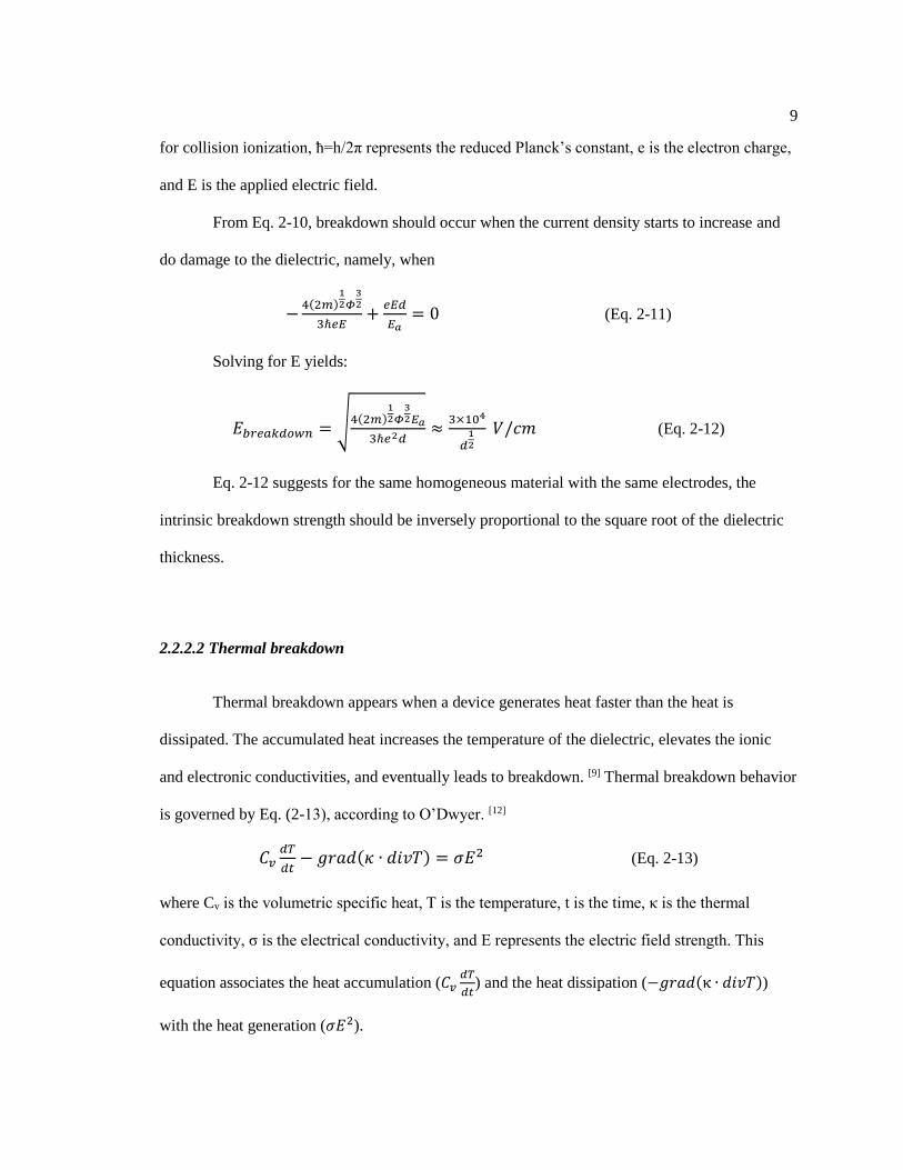
homogeneous dense sample is essential to mitigate discharge breakdown. Moulson et al. illustrate
the relationship between breakdown strengths and the relative density of high purity alumina, as
shown in Figure 2-3. [9] The dependence of breakdown strength on the relative density of the
alumina is believed to be dominated by discharge phenomenon.
11
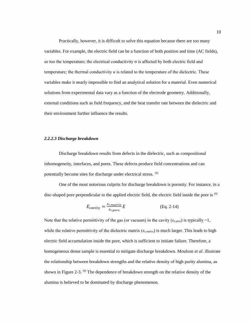
The discharge breakdown strength can also be enhanced by miniaturizing the dimensions
of the devices. This trend is observed because the smaller the sample thickness/electrode area, the
lower the possibility of a critical defect, as shown by many authors, including Moulson et al. on
high purity alumina [9] and Michael et al. in bismuth zinc niobate tantalite (BZNT) [13].
Figure 2-3: The relationship between breakdown strength and the relative density of high purity
alumina. Plot from Moulson et al. [9]
Figure 2-4: (a) The variation of electric breakdown strengths of high purity alumina with different
thicknesses. Figure reproduced from Moulson et al. [9]. (b) The leakage current versus electric field
12
In summary, high permittivity is often associated with high valence cations with
appreciable net polarizations, while outstanding breakdown strength should appear in a system
with high bandgap, short bonds, and extraordinary homogeneity.
2.2.3 Materials for dielectric energy storage
Linear dielectric materials, ferroelectric materials, relaxors, and anti-ferroelectric
materials can all be used as dielectrics.
of bismuth zinc niobate tantalate thin film with LaNiO3 (LNO) or Pt top electrodes of two different
diameters (200 µm or 2 mm). Complete breakdown happens at the upper right of the plot. Figure
adopted from the Ph.D. thesis of E. Michael. [13]
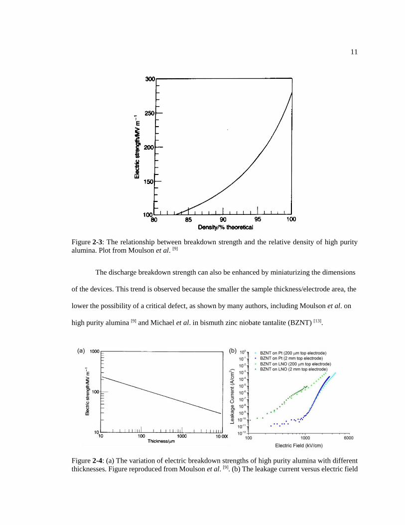
Figure 2-5: The characteristic polarization-electric field hysteresis loops for (a) linear dielectrics,
(b) ferroelectric materials, (c) relaxors, and (d) anti-ferroelectric materials. The shaded area
represents the energy storage densities in each case. (Modified figure based on Sherrit et al. [14])
13
Ferroelectric (FE) materials present switchable spontaneous polarizations under electric
fields exceeding the coercive field. [9] After most of the spontaneous polarization is re-oriented,
the polarization saturates. Upon removal of the external electric field, a remanent polarization
remains at zero field. Compared with most linear dielectric materials, ferroelectric materials have
relatively large dielectric permittivities due to the existence of the spontaneous polarization.
However, the high remanent polarizations are detrimental for energy storage because they limit
efficiency.
Relaxors are ferroelectric materials but with disrupted long-range polar order [15].
Relaxors contain polar nanoregions (PNR) with characteristic lengths scales of 2 – 20 nm,
distributed in a high polarizability matrix. Characteristically, the P-E loop of a relaxor is slimmer
than a normal ferroelectric material, with a lower remanent polarization. This makes relaxors
more suitable for energy storage capacitors as both the energy densities and the energy storage
efficiencies are improved.
Antiferroelectric (AFE) materials are characterized by “double hysteresis” in the P-E
trace as a result of sublattices with opposing polarizations within a unit cell. [16] Near zero electric
field, antiferroelectric materials have very small remanent polarizations, yielding large energy
densities. However, large hysteresis along with saturation of polarization appears at higher fields;
this reduces the potential of AFE materials as energy storage capacitors especially at high duty
cycles.
In the following sections, five materials families for dielectric energy storage are
discussed.
14
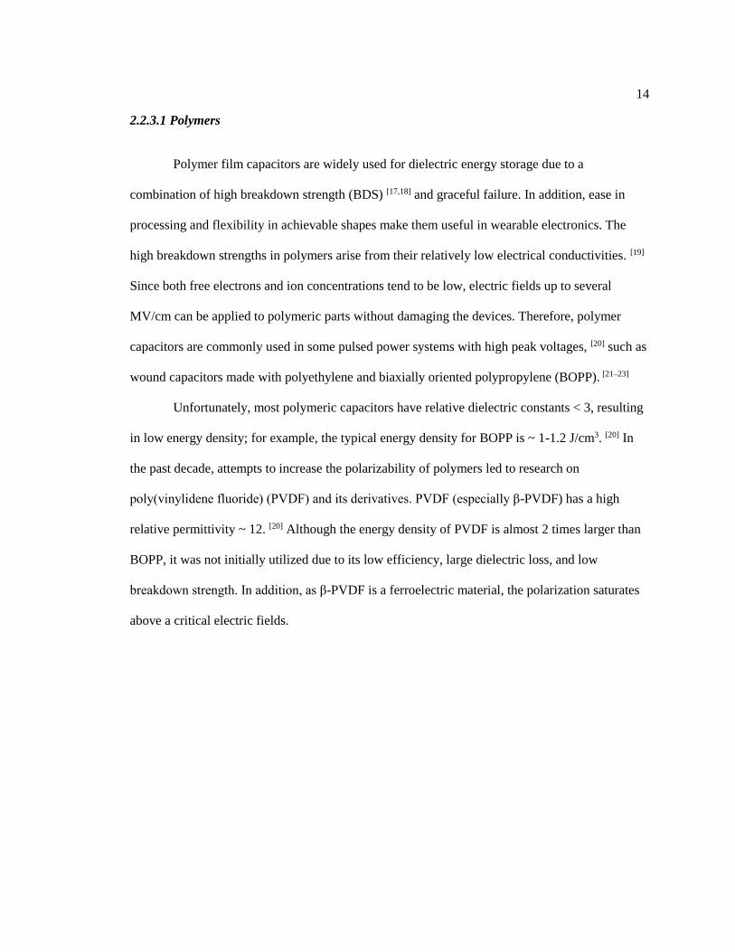
2.2.3.1 Polymers
Polymer film capacitors are widely used for dielectric energy storage due to a
combination of high breakdown strength (BDS) [17,18] and graceful failure. In addition, ease in
processing and flexibility in achievable shapes make them useful in wearable electronics. The
high breakdown strengths in polymers arise from their relatively low electrical conductivities. [19]
Since both free electrons and ion concentrations tend to be low, electric fields up to several
MV/cm can be applied to polymeric parts without damaging the devices. Therefore, polymer
capacitors are commonly used in some pulsed power systems with high peak voltages, [20] such as
wound capacitors made with polyethylene and biaxially oriented polypropylene (BOPP). [21–23]
Unfortunately, most polymeric capacitors have relative dielectric constants < 3, resulting
in low energy density; for example, the typical energy density for BOPP is ~ 1-1.2 J/cm3. [20] In
the past decade, attempts to increase the polarizability of polymers led to research on
poly(vinylidene fluoride) (PVDF) and its derivatives. PVDF (especially β-PVDF) has a high
relative permittivity ~ 12. [20] Although the energy density of PVDF is almost 2 times larger than
BOPP, it was not initially utilized due to its low efficiency, large dielectric loss, and low
breakdown strength. In addition, as β-PVDF is a ferroelectric material, the polarization saturates
above a critical electric fields.
15
The situation had drastically changed in the past 10-15 years, however. Li et al.
compared the energy storage performance of α, β, and γ-phase PVDF, finding that γ-PVDF is
more promising. Because of the reduced crystallinity produced by the β to γ transition, the
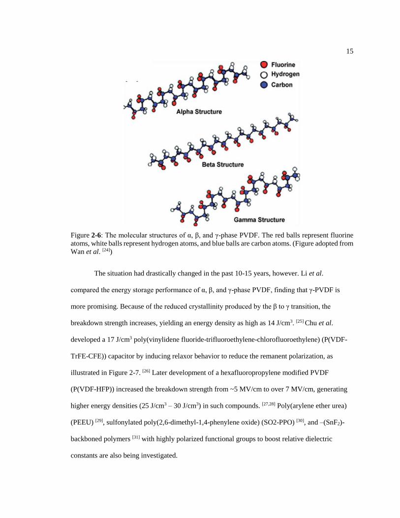
breakdown strength increases, yielding an energy density as high as 14 J/cm3. [25] Chu et al.
developed a 17 J/cm3 poly(vinylidene fluoride-trifluoroethylene-chlorofluoroethylene) (P(VDF-
TrFE-CFE)) capacitor by inducing relaxor behavior to reduce the remanent polarization, as
illustrated in Figure 2-7. [26] Later development of a hexafluoropropylene modified PVDF
(P(VDF-HFP)) increased the breakdown strength from ~5 MV/cm to over 7 MV/cm, generating
higher energy densities (25 J/cm3 – 30 J/cm3) in such compounds. [27,28] Poly(arylene ether urea)
(PEEU) [29], sulfonylated poly(2,6-dimethyl-1,4-phenylene oxide) (SO2-PPO) [30], and –(SnF2)-
backboned polymers [31] with highly polarized functional groups to boost relative dielectric
constants are also being investigated.
Figure 2-6: The molecular structures of α, β, and γ-phase PVDF. The red balls represent fluorine
atoms, white balls represent hydrogen atoms, and blue balls are carbon atoms. (Figure adopted from
Wan et al. [24])
16
2.2.3.2 Nanocomposites
To surpass the relative dielectric constants of polymer-based materials, many groups have
explored increasing the storage densities through use of filler particles in polymer matrices. Bi et
al. showed that 30 vol% BaTiO3 inclusion in mixed α and β-phase PVDF increased the energy
density from 2.5 J/cm3 to 4.1 J/cm3.[32] This increase can be attributed to the BaTiO3 filler that
raises the composite permittivity from 8 to 17, at the expense of reducing the BDS of the
composite to ~ 2 MV/cm. Similarly, Zhang et al. achieved a relative permittivity of 23 with 3
vol% TiO2@BaTiO3 (TiO2-coated BaTiO3) nanorods in PVDF, while the BDS remains above 6
MV/cm.[33] These examples illustrate that filled nanocomposites can benefit the overall energy
storage densities. As the relative permittivity and BDS are often negatively correlated (as
indicated in Figure 2-8 [34]), nanocomposites are advantageous because one can easily engineer
the volume fractions of inclusions to seek the best mixture for energy storage performance.
Figure 2-7: P-E loops for (a) P(VDF-TrFE) which is ferroelectric and (b) P(VDF-TrFE-CFE) as a
relaxor. The blue areas indicated the energy densities of the two materials. Figure by B. Chu et al. [26]
17
Nano-fillers can increase the permittivity of the composites by:
I. Utilizing the high intrinsic relative permittivity of nano-fillers to elevate the average
dielectric constants of the composites.
II. Creating additional interfaces that add to the space charge polarizations (which is
effective at low frequencies).
Proper physical models can guide design of the dielectric properties of composites with
different compositions.
Lichtenecker’s rule [9] is widely used to describe the first mechanism:
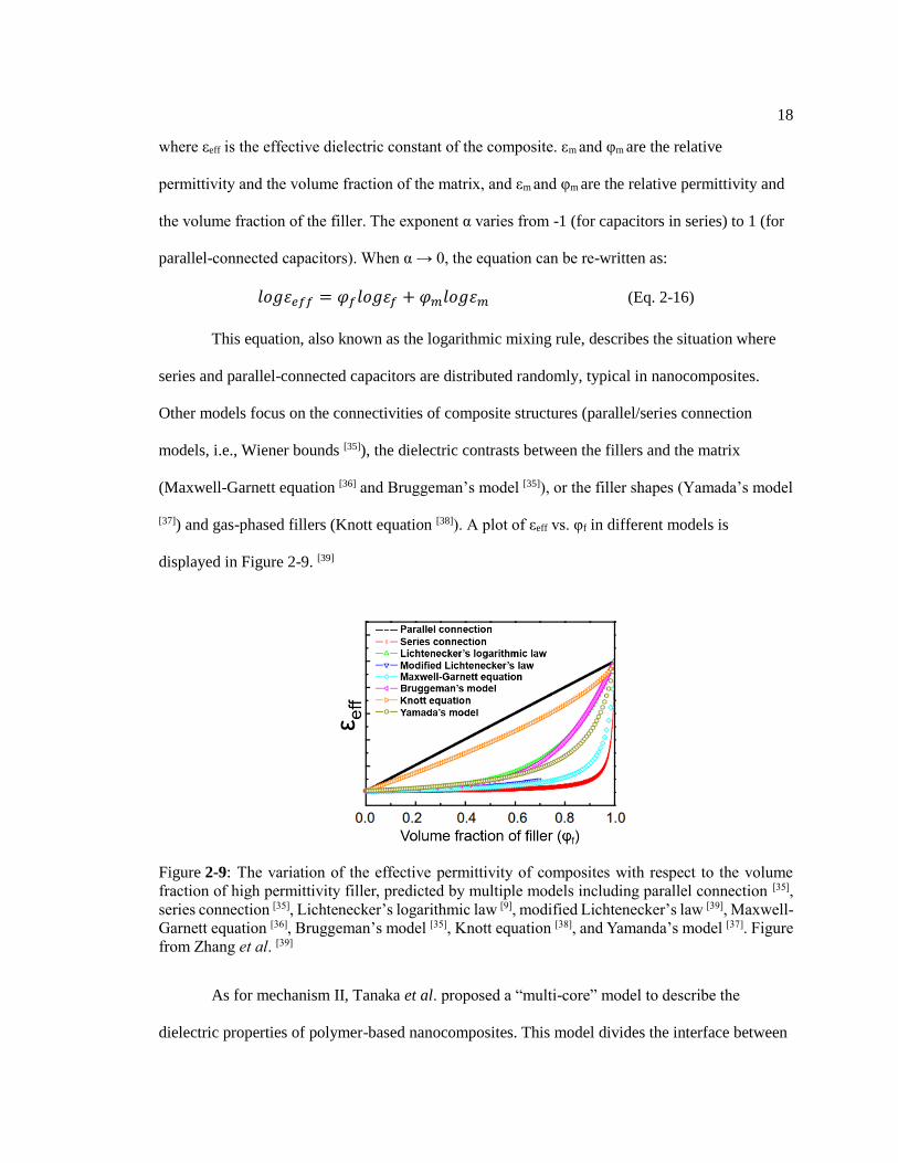
휀𝑒𝑓𝑓𝛼 = 𝜑𝑓휀𝑓
𝛼 + 𝜑𝑚휀𝑚𝛼 (Eq. 2-15)
Figure 2-8: The BDS vs relative permittivity plot for some polymers, composites, and ceramics
with antiferroelectric, ferroelectric, relaxor, or linear dielectric character. The figure shows that the
BDS and relative permittivity are inversely related in most materials. The abbreviations are:
poly(vinylidene fluoride-hexafluoropropylene) (P(VDF-HFP)), poly(vinylidene fluoride-
chlorotrifluoroethylene) (P(VDF-CTFE)), polypropylene (PP), barium strontium titanate (BST),
nanowire (NW), nanocomposite (NC), lead titanate (PT), lanthanum-doped lead zirconate stannate
titanate (PLZST), bismuth nickelate zirconate-lead titanate (BNZ-PT), lanthanum-doped lead
zirconate titanate (PLZT), barium titanate-bismuth magnesium titanate-lead zirconate (BT-BMT-
PZ), and barium titanate-bismuth scandate (BT-BS). Plot from Michael et al. [34]
18
where εeff is the effective dielectric constant of the composite. εm and φm are the relative
permittivity and the volume fraction of the matrix, and εm and φm are the relative permittivity and
the volume fraction of the filler. The exponent α varies from -1 (for capacitors in series) to 1 (for
parallel-connected capacitors). When α → 0, the equation can be re-written as:
𝑙𝑜𝑔휀𝑒𝑓𝑓 = 𝜑𝑓𝑙𝑜𝑔휀𝑓 + 𝜑𝑚𝑙𝑜𝑔휀𝑚 (Eq. 2-16)
This equation, also known as the logarithmic mixing rule, describes the situation where
series and parallel-connected capacitors are distributed randomly, typical in nanocomposites.
Other models focus on the connectivities of composite structures (parallel/series connection
models, i.e., Wiener bounds [35]), the dielectric contrasts between the fillers and the matrix
(Maxwell-Garnett equation [36] and Bruggeman’s model [35]), or the filler shapes (Yamada’s model
[37]) and gas-phased fillers (Knott equation [38]). A plot of εeff vs. φf in different models is
displayed in Figure 2-9. [39]
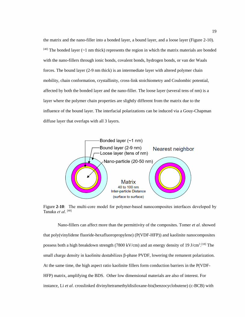
As for mechanism II, Tanaka et al. proposed a “multi-core” model to describe the
dielectric properties of polymer-based nanocomposites. This model divides the interface between
Figure 2-9: The variation of the effective permittivity of composites with respect to the volume
fraction of high permittivity filler, predicted by multiple models including parallel connection [35],
series connection [35], Lichtenecker’s logarithmic law [9], modified Lichtenecker’s law [39], Maxwell-
Garnett equation [36], Bruggeman’s model [35], Knott equation [38], and Yamanda’s model [37]. Figure
from Zhang et al. [39]
19
the matrix and the nano-filler into a bonded layer, a bound layer, and a loose layer (Figure 2-10).
[40] The bonded layer (~1 nm thick) represents the region in which the matrix materials are bonded
with the nano-fillers through ionic bonds, covalent bonds, hydrogen bonds, or van der Waals
forces. The bound layer (2-9 nm thick) is an intermediate layer with altered polymer chain
mobility, chain conformation, crystallinity, cross-link stoichiometry and Coulombic potential,
affected by both the bonded layer and the nano-filler. The loose layer (several tens of nm) is a
layer where the polymer chain properties are slightly different from the matrix due to the
influence of the bound layer. The interfacial polarizations can be induced via a Gouy-Chapman
diffuse layer that overlaps with all 3 layers.
Nano-fillers can affect more than the permittivity of the composites. Tomer et al. showed
that poly(vinylidene fluoride-hexafluoropropylene) (P(VDF-HFP)) and kaolinite nanocomposites
possess both a high breakdown strength (7800 kV/cm) and an energy density of 19 J/cm3.[18] The
small charge density in kaolinite destabilizes β-phase PVDF, lowering the remanent polarization.
At the same time, the high aspect ratio kaolinite fillers form conduction barriers in the P(VDF-
HFP) matrix, amplifying the BDS. Other low dimensional materials are also of interest. For
instance, Li et al. crosslinked divinyltetramethyldisiloxane-bis(benzocyclobutene) (c-BCB) with
Figure 2-10: The multi-core model for polymer-based nanocomposites interfaces developed by
Tanaka et al. [40]
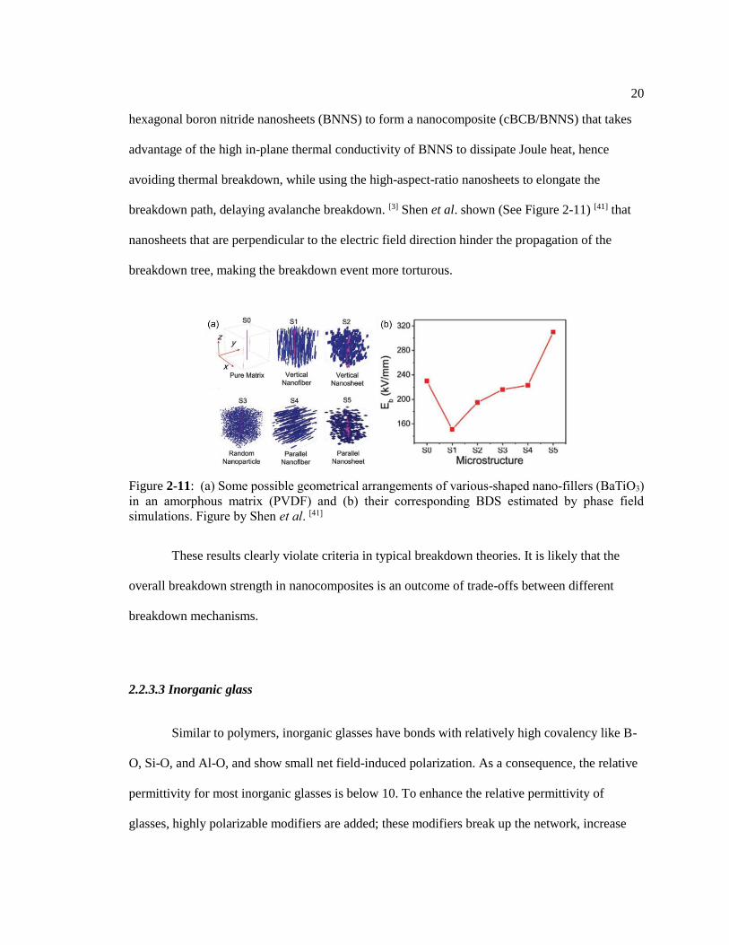
20
hexagonal boron nitride nanosheets (BNNS) to form a nanocomposite (cBCB/BNNS) that takes
advantage of the high in-plane thermal conductivity of BNNS to dissipate Joule heat, hence
avoiding thermal breakdown, while using the high-aspect-ratio nanosheets to elongate the
breakdown path, delaying avalanche breakdown. [3] Shen et al. shown (See Figure 2-11) [41] that
nanosheets that are perpendicular to the electric field direction hinder the propagation of the
breakdown tree, making the breakdown event more torturous.
These results clearly violate criteria in typical breakdown theories. It is likely that the
overall breakdown strength in nanocomposites is an outcome of trade-offs between different
breakdown mechanisms.
2.2.3.3 Inorganic glass
Similar to polymers, inorganic glasses have bonds with relatively high covalency like B-
O, Si-O, and Al-O, and show small net field-induced polarization. As a consequence, the relative
permittivity for most inorganic glasses is below 10. To enhance the relative permittivity of
glasses, highly polarizable modifiers are added; these modifiers break up the network, increase
Figure 2-11: (a) Some possible geometrical arrangements of various-shaped nano-fillers (BaTiO3)
in an amorphous matrix (PVDF) and (b) their corresponding BDS estimated by phase field
simulations. Figure by Shen et al. [41]
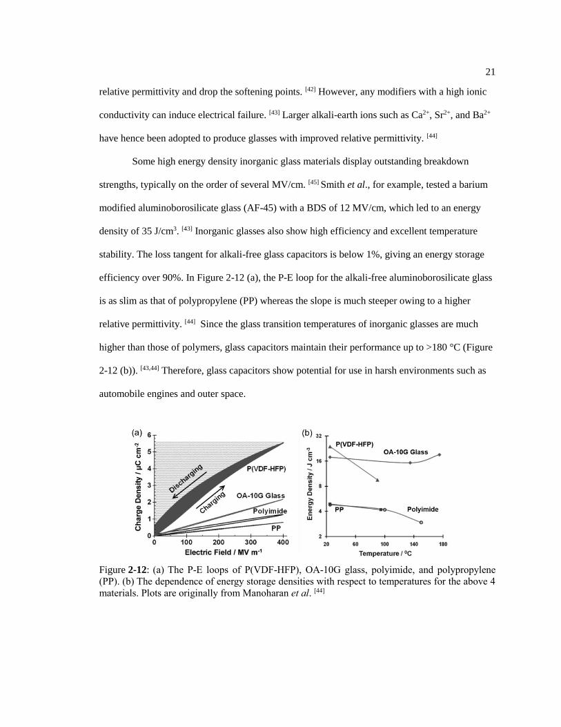
21
relative permittivity and drop the softening points. [42] However, any modifiers with a high ionic
conductivity can induce electrical failure. [43] Larger alkali-earth ions such as Ca2+, Sr2+, and Ba2+
have hence been adopted to produce glasses with improved relative permittivity. [44]
Some high energy density inorganic glass materials display outstanding breakdown
strengths, typically on the order of several MV/cm. [45] Smith et al., for example, tested a barium
modified aluminoborosilicate glass (AF-45) with a BDS of 12 MV/cm, which led to an energy
density of 35 J/cm3. [43] Inorganic glasses also show high efficiency and excellent temperature
stability. The loss tangent for alkali-free glass capacitors is below 1%, giving an energy storage
efficiency over 90%. In Figure 2-12 (a), the P-E loop for the alkali-free aluminoborosilicate glass
is as slim as that of polypropylene (PP) whereas the slope is much steeper owing to a higher
relative permittivity. [44] Since the glass transition temperatures of inorganic glasses are much
higher than those of polymers, glass capacitors maintain their performance up to >180 °C (Figure
2-12 (b)). [43,44] Therefore, glass capacitors show potential for use in harsh environments such as
automobile engines and outer space.
Figure 2-12: (a) The P-E loops of P(VDF-HFP), OA-10G glass, polyimide, and polypropylene
(PP). (b) The dependence of energy storage densities with respect to temperatures for the above 4
materials. Plots are originally from Manoharan et al. [44]
22
2.2.3.4 Bulk ceramics
Appropriately formulated ceramic materials have a high dielectric permittivity, which
provides better energy storage performance at lower fields. BaTiO3, a widely used dielectric
ceramic has a room temperature permittivity over 1000 [19],[46] There have been reports on TiO2-
based ceramics with III-V cation complexes (In3+-Nb5+ or Pr3+-Nb5+) that showed colossal relative
permittivity on the order of 104. [47–49] However, the losses of those systems are also 1-2 orders of
magnitude higher than conventional energy storage materials, making these compounds
unsuitable for energy storage applications. In fact, many reported bulk ceramics with high energy
densities have relative dielectric constants between several hundreds and low thousands (Figure
2-13). [50–70].
The energy densities in Figure 2-13 are on average lower than the values from PVDF-
based polymer and nanocomposite films because bulk ceramic samples are generally 100 µm – 1
cm thick. The thickness dependence described in section 2.2.2.3 significantly diminishes the BDS
of bulk ceramics. Typical BDS for bulk ceramics are less than 1 MV/cm.
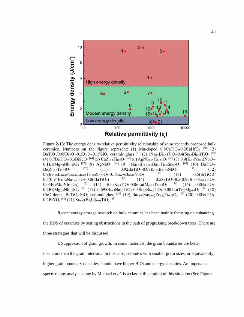
23
Recent energy storage research on bulk ceramics has been mainly focusing on enhancing
the BDS of ceramics by setting obstructions in the path of progressing breakdown trees. There are
three strategies that will be discussed.
I. Suppression of grain growth: In some materials, the grain boundaries are better
insulators than the grain interiors. In this case, ceramics with smaller grain sizes, or equivalently,
higher grain boundary densities, should have higher BDS and energy densities. An impedance
spectroscopy analysis done by Michael et al. is a classic illustration of this situation (See Figure
Figure 2-13: The energy density-relative permittivity relationship of some recently proposed bulk
ceramics. Numbers on the figure represent: (1) Mn-doped 0.8CaTiO3-0.2CaHfO3 [50] (2)
BaTiO3/0.65Bi2O3-0.2B2O3-0.15SiO2 ceramic glass [51] (3) (Na0.5Bi0.5)TiO3-0.4(Sr0.7Bi0.2)TiO3 [62]
(4) 0.7BaTiO3-0.3BiScO3 [64] (5) CaZr0.8Ti0.2O3 [65] (6) AgNb0.85Ta0.15O3 [66] (7) 0.9(K0.5Na0.5)NbO3-
0.1Bi(Mg2/3Nb1/3)O3 [67] (8) AgNbO3 [68] (9) (Na0.5Bi0.5)0.8Ba0.2Ti0.8Sn0.2O3 [69] (10) BaTiO3-
Bi(Zn0.5Ti0.5)O3 [70] (11) 0.92BaTiO3-0.08K0.73Bi0.09NbO3 [52] (12)
0.9Bi0.48La0.02Na0.48Li0.02Ti0.98Zr0.02O3-0.1Na0.73Bi0.09NbO3 [53] (13) 0.5(SrTiO3)-
0.5(0.94Bi0.54Na0.46TiO3-0.06BaTiO3) [54] (14) 0.5SrTiO3-0.5(0.95Bi0.5Na0.5TiO3-
0.05BaAl0.5Nb0.5O3) [55] (15) Bi0.5K0.5TiO3-0.06La(Mg0.5Ti0.5)O3 [56] (16) 0.8BaTiO3-
0.2Bi(Mg2/3Nb1/3)O3 [57] (17) 0.695Bi0.5Na0.5TiO3-0.3Sr0.7Bi0.2TiO3-0.005LaTi0.5Mg0.5O3 [58] (18)
CuO-doped BaTiO3-SiO2 ceramic-glass [59] (19) Ba0.997Sm0.002Zr0.15Ti0.85O3 [60] (20) 0.8BaTiO3-
0.2BiYO3 [61] (21) Sr0.92(Bi,Li)0.08TiO3 [63].
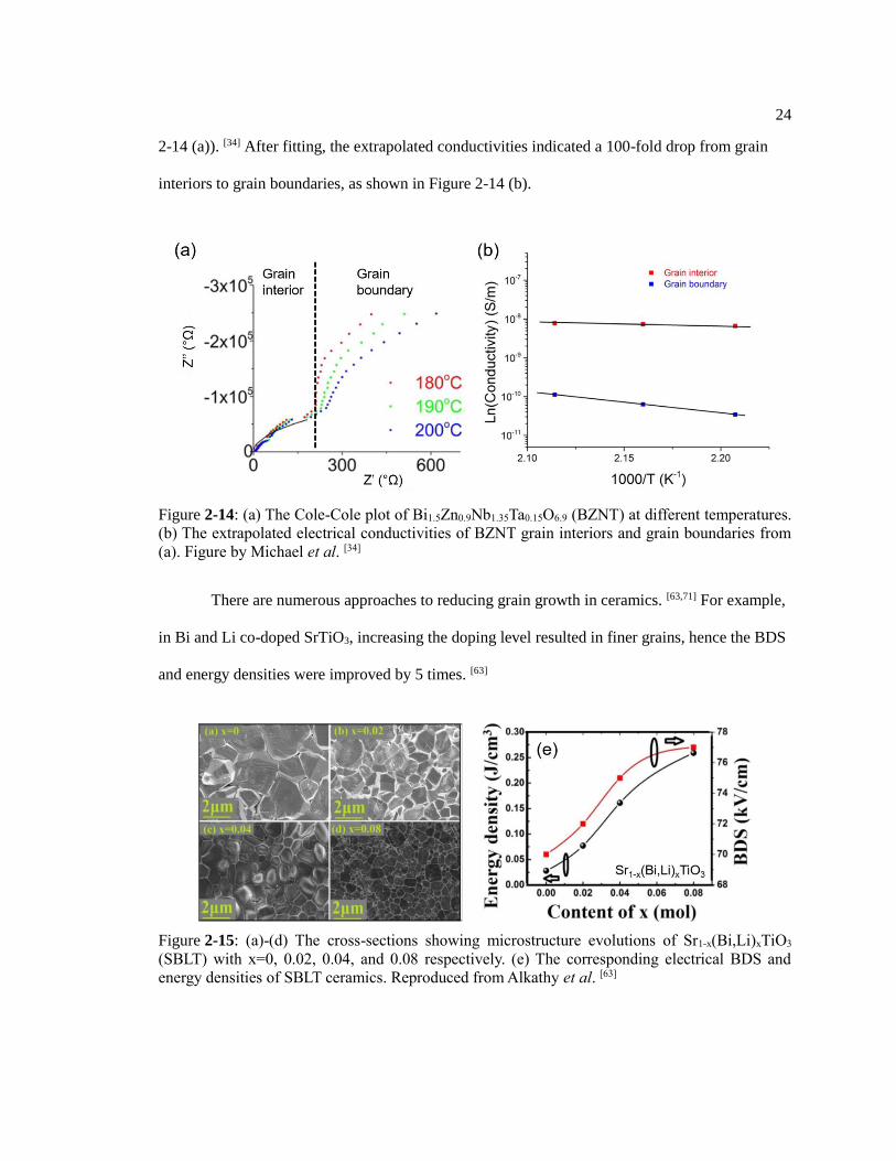
24
2-14 (a)). [34] After fitting, the extrapolated conductivities indicated a 100-fold drop from grain
interiors to grain boundaries, as shown in Figure 2-14 (b).
There are numerous approaches to reducing grain growth in ceramics. [63,71] For example,
in Bi and Li co-doped SrTiO3, increasing the doping level resulted in finer grains, hence the BDS
and energy densities were improved by 5 times. [63]
Figure 2-14: (a) The Cole-Cole plot of Bi1.5Zn0.9Nb1.35Ta0.15O6.9 (BZNT) at different temperatures.
(b) The extrapolated electrical conductivities of BZNT grain interiors and grain boundaries from
(a). Figure by Michael et al. [34]
Figure 2-15: (a)-(d) The cross-sections showing microstructure evolutions of Sr1-x(Bi,Li)xTiO3
(SBLT) with x=0, 0.02, 0.04, and 0.08 respectively. (e) The corresponding electrical BDS and
energy densities of SBLT ceramics. Reproduced from Alkathy et al. [63]
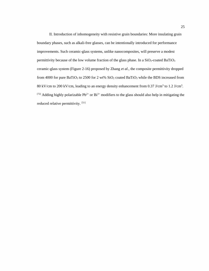
25
II. Introduction of inhomogeneity with resistive grain boundaries: More insulating grain
boundary phases, such as alkali-free glasses, can be intentionally introduced for performance
improvements. Such ceramic-glass systems, unlike nanocomposites, will preserve a modest
permittivity because of the low volume fraction of the glass phase. In a SiO2-coated BaTiO3
ceramic-glass system (Figure 2-16) proposed by Zhang et al., the composite permittivity dropped
from 4000 for pure BaTiO3 to 2500 for 2 wt% SiO2 coated BaTiO3 while the BDS increased from
80 kV/cm to 200 kV/cm, leading to an energy density enhancement from 0.37 J/cm3 to 1.2 J/cm3.
[72] Adding highly polarizable Pb2+ or Bi3+ modifiers to the glass should also help in mitigating the
reduced relative permittivity. [51]
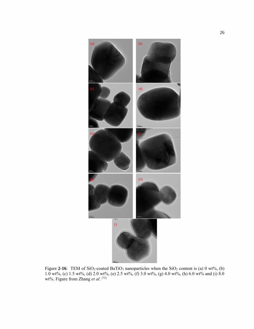
26
Figure 2-16: TEM of SiO2-coated BaTiO3 nanoparticles when the SiO2 content is (a) 0 wt%, (b)
1.0 wt%, (c) 1.5 wt%, (d) 2.0 wt%, (e) 2.5 wt%, (f) 3.0 wt%, (g) 4.0 wt%, (h) 6.0 wt% and (i) 8.0
wt%. Figure from Zhang et al. [72]
27
III. Phase engineering of complex oxides: By stabilizing certain phase(s), it is possible to
tune the energy storage performance of materials. For example, it is well-known that AFE
materials are suitable for energy storage up to the electric field that switches the spontaneous
polarization. If the re-orientation of polarization can be delayed in an antiferroelectric, the energy
density should increase accordingly, as illustrated by Figure 2-17. This idea was successfully
demonstrated by Zhao et al. in Ta-doped silver niobate. [66]
In addition, facilitating the appearance of polar nanoregions (PNR) in relaxors is also
effective in improving energy storage ceramics. This is achieved by substituting aliovalent
cations on the same site to destroy the long-range polar order in the ceramics [73], thus often
leading to compositions of high complexity. [55,60]
2.2.3.5 Thin film ceramics
Thin film ceramic capacitors have become a popular topic in recent years in part due to
intensifying needs for electronics miniaturization. Films can be grown by multiple deposition
Figure 2-17: (a) The P-E loops of AgNbO3 and 15 mol% Ta5+-doped AgNbO3. The shaded areas
indicate the recoverable energy densities. (b) The recoverable energy storage densities (Wrec) and
corresponding energy storage efficiencies of AgNbO3 with dependence of Ta doping levels. (Figure
from Zhao et al. [66])
28
methods, including chemical solution deposition [74], sputtering [6], pulsed laser deposition [75], and
atomic layer deposition [76]. In addition, as the thicknesses of ceramic thin films can be precisely
controlled between 10 nm and several microns, it is possible to integrate some thin film
capacitors on flexible substrates such as mica [77], metal foils [5], and polyimide [2], which could
enable the commercialization of wearable electronics.
The strategies to elevate energy storage densities in bulk ceramics also apply to films.
[75,78] Additionally, with the decrease of sample dimensions, thin film ceramics present
significantly higher BDS than bulk specimen since there is less of a chance that critical defects
will appear in the thin films. In cases where the breakdown strengths of ceramic thin films can be
engineered to be comparable to those of polymer and nanocomposite films, very large energy
storage densities can be achieved. For example, Hu et al. demonstrated an antiferroelectric La-
doped lead zirconate titanate (PLZT) thin film with an energy storage density of 61 J/cm3 at 4.3
MV/cm [79]. Ta-doped bismuth zinc niobate (BZNT) films also show a high energy density (67
J/cm3) and high breakdown strength (6.1 MV/cm) [34].
Specifically for thin films, the interactions between films and substrates, or between films
of different compositions can also play an important role. Recently, ultrahigh energy densities
were achieved in films deposited on defect engineered substrates. For instance, SrTiO3 on
La0.67Sr0.33MnO3 substrate (STO/LSMO) had been proposed to exhibit an energy density as large
as 307 J/cm3 at 6.6 MV/cm due to the increased BDS via interfacial local electric field re-
distribution induced within the inter-diffusion layer between STM and LSMO. [80] Another case
that is akin to STO/LSMO was demonstrated in aluminum/amorphous alumina (Al/AmAO) films
where residual AmAO depressed the leakage current of dense crystalline Al2O3. [81] In terms of
film-film interactions, sandwich structured multilayer films were claimed to be effective in
enhancing energy densities. These systems succeeded by either tuning the permittivity-BDS
29
relationships (like nanocomposites) [82] or using one layer as a template to control the morphology
of the other layer. [83]
Although the energy densities reported in thin film ceramic capacitors are much larger
than those of bulk materials, it is often unfair to compare the numbers with those of polymers,
nanocomposites, glasses, and bulk ceramics. This is because almost all the reported values for
thin films are measured at 1 kHz – 10 kHz, while for other materials frequency ranges from 1-10
Hz are used. High frequency P-E loops tend to significantly inflate the maximum achievable
electric fields, but demonstrate the potentials for high power density applications. Secondly, in
most thin films, the volume of the substrate is ignored in calculating the energy density.
Therefore, it makes more sense to state thin films are more competitive for low voltage devices
with outstanding power densities while polymers, nanocomposites, glasses, and bulk ceramics are
suitable for storing a large amount of energy in a high-voltage, lower-power system.
One common drawback of bulk and thin film ceramic capacitors is the high processing
temperatures. Most bulk ceramics are sintered at >1000 °C [67,84] while many films are crystallized
above ~ 500 °C.[13,75,79,85] These temperatures exceed the decomposition temperatures of polymer
substrates. Base metal substrates such as Ni, Cu, and Al foil are also susceptible to oxidation at
these temperatures. Michael-Sapia et al. reported a BZNT film with a maximum heat treatment
temperature of 350 °C [2] in which the presence of nanocrystallites increased the permittivity.
These films showed a dielectric constant of ~ 50 and an energy density ~ 40 J/cm3 under an
applied field of 4 MV/cm [2]. It was suggested by Michael-Sapia et al. that the crystalline phase is
based on δ-Bi2O3 [2]. δ-Bi2O3 is a fluorite structured phase that is only thermodynamically stable
at high temperature but can be stabilized at room temperature with Nb doping [86]. One possible
chemical formula of Nb-doped δ-Bi2O3 is Bi3NbO7 [86]. Inspired by Michael-Sapia’s work,
Bi3NbO7 thin films were made to study the energy storage behavior of this material.
30
2.3 Experimental procedures
0.1 mol/L BNO (Bi3NbO7) sol-gel solutions were made using Pechini’s method, based on
the research of Michael-Sapia et al. [2]. First, bismuth nitrate pentahydrate (Sigma-Aldrich Corp.,
St. Louis, MO) and niobium ethoxide (Sigma-Aldrich) were dissolved separately into two flasks
of anhydrous ethylene glycol (Sigma-Aldrich) in a N2 filled glove box. For tungsten or tantalum-
doped solutions, tungsten (VI) ethoxide (Sigma-Aldrich) or tantalum (V) ethoxide (Sigma-
Aldrich) was added to the niobium ethoxide flask. Then citric acid (Sigma-Aldrich) was added to
both of the flasks so as to stabilize the precursors. The molar ratio of organometallic precursors
and citric acid is 2:1. Finally, the solution in the Nb flask was added to the Bi flask. While the
solutions were stable (without precipitation) for periods of up to a year, it was found that the
viscosity changed over time, resulting in thicker films from aged solutions.
Chemical solution deposition processes were used for the fabrication of the BNO thin
films, as shown in Figure 2-18. A 5 µm filter was used during the deposition. The BNO solution
was spin cast on platinized silicon wafers (Pt (150 nm)/Ti (20 nm)/SiO2 (500 nm)/Si, NOVA
Electronic Materials, Flower Mound, TX) at a speed of 4000 rpm for 40 sec, followed by a drying
procedure on the hotplate at 250 °C for 3 min. The samples were then heated on the hotplate at
temperatures varied from 350 °C to 450 °C for 10 min. The hot plate temperatures were
calibrated using a thermometer embedded in the hot plate for temperatures below 250 °C. At
higher temperatures, a thermocouple was placed on the hot plate surface to provide a more
accurate measurement. The heat treatments occurred after the deposition of each layer of BNO
solution and 5 cycles of deposition/heat treatment cycles were used to build up a film thickness of
~ 120-140 nm. Some films were exposed to UV radiation to improve organic removal. For this
purpose, a 260 nm, 385 mW ultra-violet (Fusion DUV system, Heraeus Noblelight America LLC,
Gaithersburg, MD) exposure, with the substrate held at 60°C for 3 min in air was added between
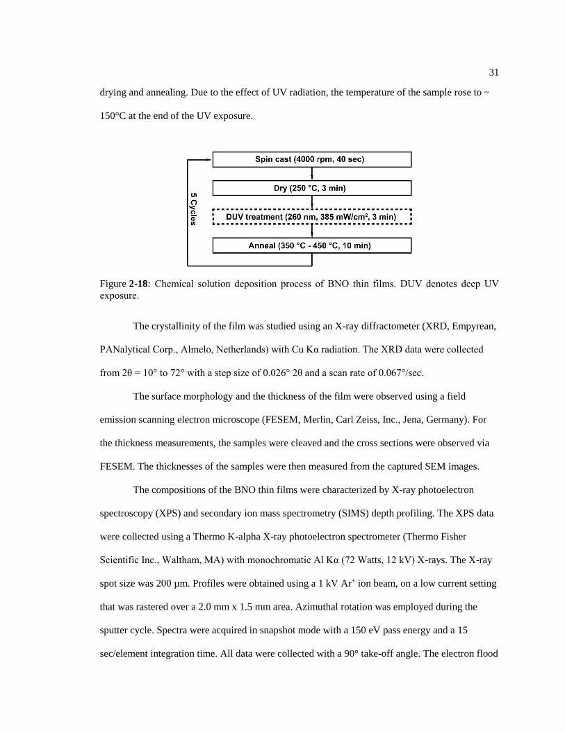
31
drying and annealing. Due to the effect of UV radiation, the temperature of the sample rose to ~
150°C at the end of the UV exposure.
The crystallinity of the film was studied using an X-ray diffractometer (XRD, Empyrean,
PANalytical Corp., Almelo, Netherlands) with Cu Kα radiation. The XRD data were collected
from 2θ = 10° to 72° with a step size of 0.026° 2θ and a scan rate of 0.067°/sec.
The surface morphology and the thickness of the film were observed using a field
emission scanning electron microscope (FESEM, Merlin, Carl Zeiss, Inc., Jena, Germany). For
the thickness measurements, the samples were cleaved and the cross sections were observed via
FESEM. The thicknesses of the samples were then measured from the captured SEM images.
The compositions of the BNO thin films were characterized by X-ray photoelectron
spectroscopy (XPS) and secondary ion mass spectrometry (SIMS) depth profiling. The XPS data
were collected using a Thermo K-alpha X-ray photoelectron spectrometer (Thermo Fisher
Scientific Inc., Waltham, MA) with monochromatic Al Kα (72 Watts, 12 kV) X-rays. The X-ray
spot size was 200 µm. Profiles were obtained using a 1 kV Ar+ ion beam, on a low current setting
that was rastered over a 2.0 mm x 1.5 mm area. Azimuthal rotation was employed during the
sputter cycle. Spectra were acquired in snapshot mode with a 150 eV pass energy and a 15
sec/element integration time. All data were collected with a 90° take-off angle. The electron flood
Figure 2-18: Chemical solution deposition process of BNO thin films. DUV denotes deep UV
exposure.
32
gun with standard settings (0.4 V beam voltage, 100 µA emission) was used for charge
compensation. The data were processed with the Thermo Advantage software.
The SIMS data were collected using an IonTof IV secondary ion mass spectrometer (Ion-
Tof GmbH, Münster, Germany). Negative ion profiles were collected with 25kV Bi+ primary ions
(1.2 pA) and a 1 kV Cs+ sputter beam (100 nA). The primary ions were rastered over a 150 µm x
150 µm area with a pixel density of 128 pixels x 128 pixels and the Cs+ beam was rastered over a
400 µm x 400 µm area. The analysis area was centered in the sputter area and profiles were
collected in interlace mode. A cycle time of 60 µsec was employed which resulted in a mass
range of 0-323 Da. The data were processed using the IonTof-SurfaceLab 6.6 software.
A spectroscopic ellipsometer (M-2000, J. A. Woollam Co., Lincoln, NE) was used to
characterize the optical properties of the BNO thin films as well as quantifying the porosity of the
non-UV treated BNO thin film. Data within wavelengths from 400 nm to 1690 nm and 3 incident
angles (55°, 65° and 75°) were collected and fitted with CompleteEASE software (J. A. Woollam
Co.). A stack of BNO/intermix/Pt model was utilized to fit the ellipsometry data. A Sellmeier
model was initially applied to fit the BNO layer over the wavelength range where the film was
transparent; these data were used to help parameterize the optical properties to a general oscillator
model by Tauc-Lorentz function. Assuming 100% density for 450 °C-annealed UV treated BNO,
the porosity of the 450 °C-annealed non-UV treated BNO thin film was calculated by replacing
the BNO layer with an effective medium layer of BNO and void.
For electrical measurements, 50 nm thick sputtered Pt top electrodes (CMS-18 Sputter
System, Kurt J. Lesker Company, Pittsburgh, PA) were patterned using a double layer
lithography process. The diameter of the circular electrodes was 200 µm. After the lift-off
process, the film was annealed in a rapid thermal annealing (RTA) furnace (RTP-600S, Modular
Process Technology Corp., San Jose, CA) at 300 °C for 10 min.
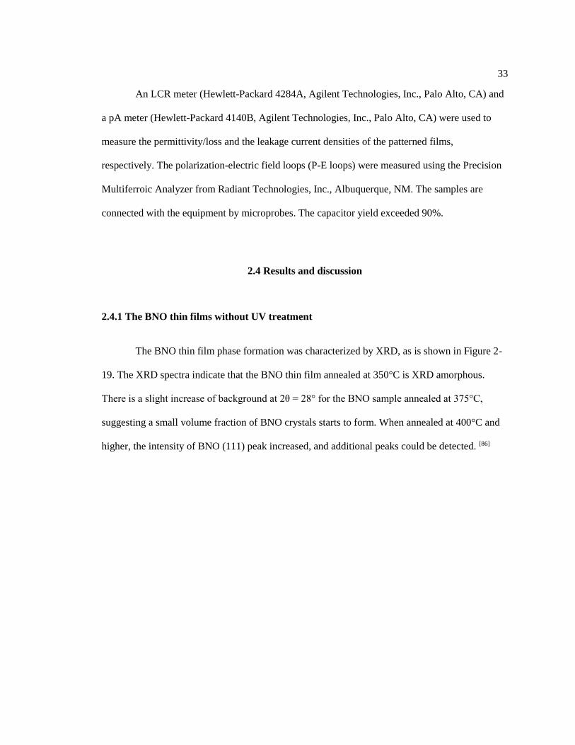
33
An LCR meter (Hewlett-Packard 4284A, Agilent Technologies, Inc., Palo Alto, CA) and
a pA meter (Hewlett-Packard 4140B, Agilent Technologies, Inc., Palo Alto, CA) were used to
measure the permittivity/loss and the leakage current densities of the patterned films,
respectively. The polarization-electric field loops (P-E loops) were measured using the Precision
Multiferroic Analyzer from Radiant Technologies, Inc., Albuquerque, NM. The samples are
connected with the equipment by microprobes. The capacitor yield exceeded 90%.
2.4 Results and discussion
2.4.1 The BNO thin films without UV treatment
The BNO thin film phase formation was characterized by XRD, as is shown in Figure 2-
19. The XRD spectra indicate that the BNO thin film annealed at 350°C is XRD amorphous.
There is a slight increase of background at 2θ = 28° for the BNO sample annealed at 375°C,
suggesting a small volume fraction of BNO crystals starts to form. When annealed at 400°C and
higher, the intensity of BNO (111) peak increased, and additional peaks could be detected. [86]
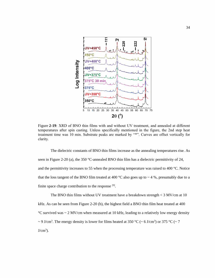
34
The dielectric constants of BNO thin films increase as the annealing temperatures rise. As
seen in Figure 2-20 (a), the 350 °C-annealed BNO thin film has a dielectric permittivity of 24,
and the permittivity increases to 55 when the processing temperature was raised to 400 °C. Notice
that the loss tangent of the BNO film treated at 400 °C also goes up to ~ 4 %, presumably due to a
finite space charge contribution to the response [9].
The BNO thin films without UV treatment have a breakdown strength < 3 MV/cm at 10
kHz. As can be seen from Figure 2-20 (b), the highest field a BNO thin film heat treated at 400
°C survived was ~ 2 MV/cm when measured at 10 kHz, leading to a relatively low energy density
~ 9 J/cm3. The energy density is lower for films heated at 350 °C (~ 6 J/cm3) or 375 °C (~ 7
J/cm3).
Figure 2-19: XRD of BNO thin films with and without UV treatment, and annealed at different
temperatures after spin casting. Unless specifically mentioned in the figure, the 2nd step heat
treatment time was 10 min. Substrate peaks are marked by “*”. Curves are offset vertically for
clarity.
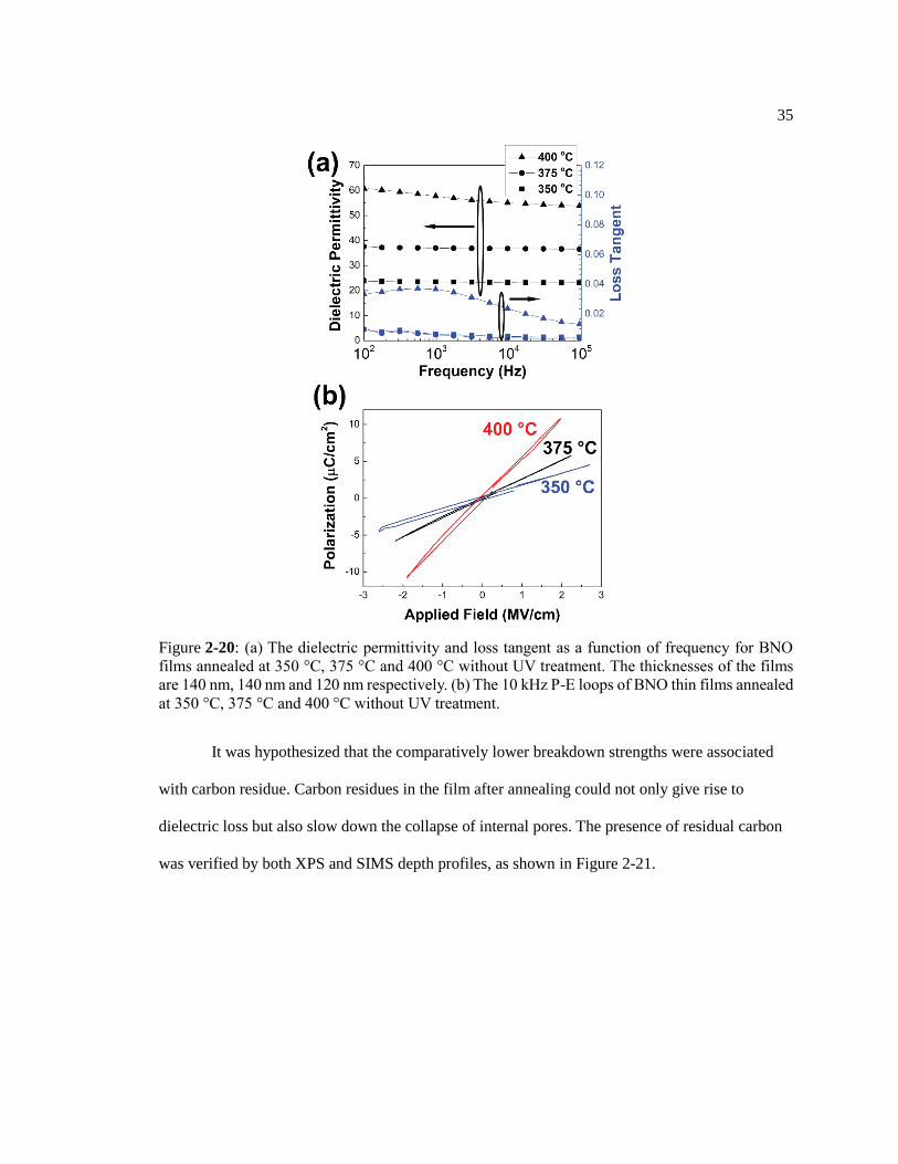
35
It was hypothesized that the comparatively lower breakdown strengths were associated
with carbon residue. Carbon residues in the film after annealing could not only give rise to
dielectric loss but also slow down the collapse of internal pores. The presence of residual carbon
was verified by both XPS and SIMS depth profiles, as shown in Figure 2-21.
Figure 2-20: (a) The dielectric permittivity and loss tangent as a function of frequency for BNO
films annealed at 350 °C, 375 °C and 400 °C without UV treatment. The thicknesses of the films
are 140 nm, 140 nm and 120 nm respectively. (b) The 10 kHz P-E loops of BNO thin films annealed
at 350 °C, 375 °C and 400 °C without UV treatment.
36
Figure 2-21: (a) Overlay of the carbon XPS depth profiles of BNO thin films annealed at 350 °C
with and without UV treatment. (b) The SIMS depth profiles of the BNO thin films treated without
UV exposure and annealed at 350 °C. (c) The SIMS depth profiles of the BNO thin films treated
with UV exposure and annealed at 350 °C.
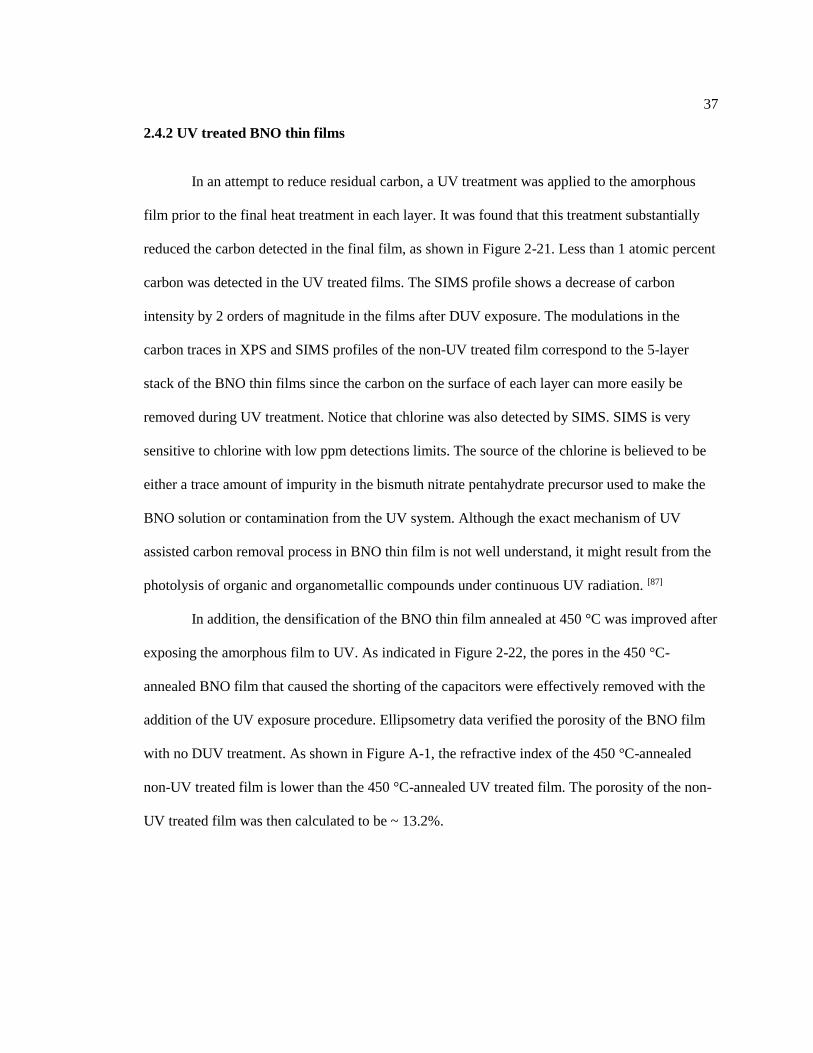
37
2.4.2 UV treated BNO thin films
In an attempt to reduce residual carbon, a UV treatment was applied to the amorphous
film prior to the final heat treatment in each layer. It was found that this treatment substantially
reduced the carbon detected in the final film, as shown in Figure 2-21. Less than 1 atomic percent
carbon was detected in the UV treated films. The SIMS profile shows a decrease of carbon
intensity by 2 orders of magnitude in the films after DUV exposure. The modulations in the
carbon traces in XPS and SIMS profiles of the non-UV treated film correspond to the 5-layer
stack of the BNO thin films since the carbon on the surface of each layer can more easily be
removed during UV treatment. Notice that chlorine was also detected by SIMS. SIMS is very
sensitive to chlorine with low ppm detections limits. The source of the chlorine is believed to be
either a trace amount of impurity in the bismuth nitrate pentahydrate precursor used to make the
BNO solution or contamination from the UV system. Although the exact mechanism of UV
assisted carbon removal process in BNO thin film is not well understand, it might result from the
photolysis of organic and organometallic compounds under continuous UV radiation. [87]
In addition, the densification of the BNO thin film annealed at 450 °C was improved after
exposing the amorphous film to UV. As indicated in Figure 2-22, the pores in the 450 °C-
annealed BNO film that caused the shorting of the capacitors were effectively removed with the
addition of the UV exposure procedure. Ellipsometry data verified the porosity of the BNO film
with no DUV treatment. As shown in Figure A-1, the refractive index of the 450 °C-annealed
non-UV treated film is lower than the 450 °C-annealed UV treated film. The porosity of the non-
UV treated film was then calculated to be ~ 13.2%.
38
Possibly due to the removal of residual carbon in the films, the crystallinity of the UV
treated BNO thin films increased when treated films were annealed ≥ 375 °C. As can be seen
from Figure 2-19, the UV treated BNO thin film annealed at 375 °C has higher XRD peak
intensities than those without the UV treatment. Also, as apparent in Table 2-1, the UV treated
BNO thin films show smaller full width at half maximum (FWHM) values than the samples
without UV exposure. This suggests the crystallite sizes are larger for the BNO thin films treated
Figure 2-22: The top-down FESEM images of BNO thin films (a) annealed at 450 °C without UV
treatment and (b) annealed at 450 °C with the UV treatment procedure.
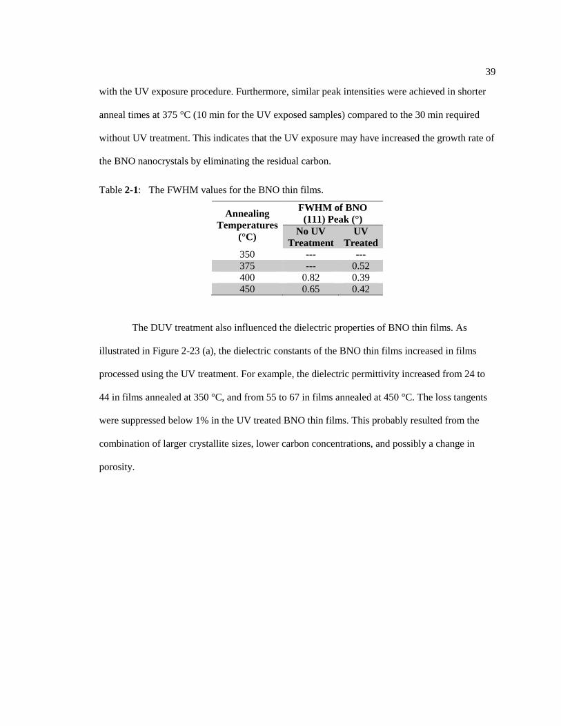
39
with the UV exposure procedure. Furthermore, similar peak intensities were achieved in shorter
anneal times at 375 °C (10 min for the UV exposed samples) compared to the 30 min required
without UV treatment. This indicates that the UV exposure may have increased the growth rate of
the BNO nanocrystals by eliminating the residual carbon.
The DUV treatment also influenced the dielectric properties of BNO thin films. As
illustrated in Figure 2-23 (a), the dielectric constants of the BNO thin films increased in films
processed using the UV treatment. For example, the dielectric permittivity increased from 24 to
44 in films annealed at 350 °C, and from 55 to 67 in films annealed at 450 °C. The loss tangents
were suppressed below 1% in the UV treated BNO thin films. This probably resulted from the
combination of larger crystallite sizes, lower carbon concentrations, and possibly a change in
porosity.
Table 2-1: The FWHM values for the BNO thin films.
Annealing
Temperatures
(°C)
FWHM of BNO
(111) Peak (°)
No UV
Treatment
UV
Treated 350 --- ---
375 --- 0.52
400 0.82 0.39
450 0.65 0.42
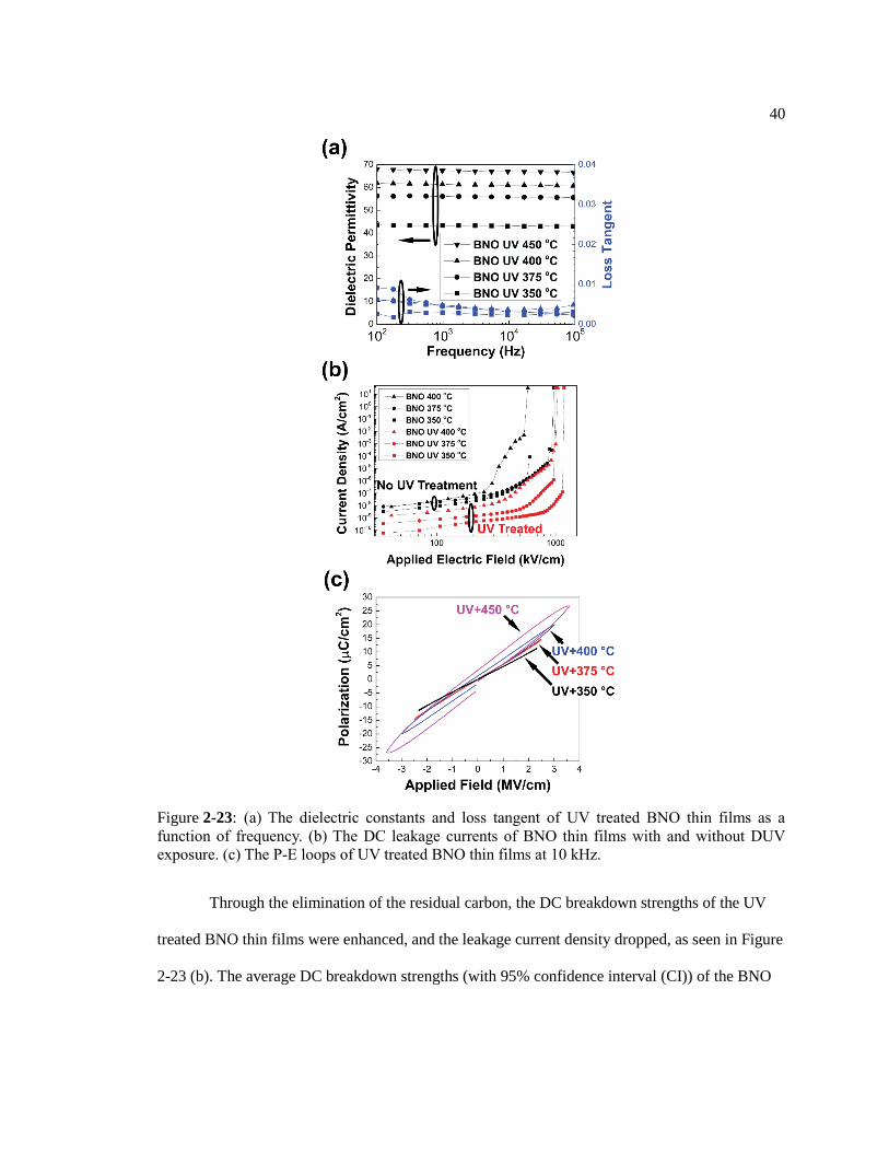
40
Through the elimination of the residual carbon, the DC breakdown strengths of the UV
treated BNO thin films were enhanced, and the leakage current density dropped, as seen in Figure
2-23 (b). The average DC breakdown strengths (with 95% confidence interval (CI)) of the BNO
Figure 2-23: (a) The dielectric constants and loss tangent of UV treated BNO thin films as a
function of frequency. (b) The DC leakage currents of BNO thin films with and without DUV
exposure. (c) The P-E loops of UV treated BNO thin films at 10 kHz.
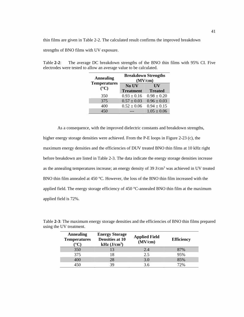
41
thin films are given in Table 2-2. The calculated result confirms the improved breakdown
strengths of BNO films with UV exposure.
As a consequence, with the improved dielectric constants and breakdown strengths,
higher energy storage densities were achieved. From the P-E loops in Figure 2-23 (c), the
maximum energy densities and the efficiencies of DUV treated BNO thin films at 10 kHz right
before breakdown are listed in Table 2-3. The data indicate the energy storage densities increase
as the annealing temperatures increase; an energy density of 39 J/cm3 was achieved in UV treated
BNO thin film annealed at 450 °C. However, the loss of the BNO thin film increased with the
applied field. The energy storage efficiency of 450 °C-annealed BNO thin film at the maximum
applied field is 72%.
Table 2-2: The average DC breakdown strengths of the BNO thin films with 95% CI. Five
electrodes were tested to allow an average value to be calculated.
Annealing
Temperatures
(°C)
Breakdown Strengths
(MV/cm)
No UV
Treatment
UV
Treated 350 0.93 ± 0.16 0.98 ± 0.20
375 0.57 ± 0.03 0.96 ± 0.03
400 0.52 ± 0.06 0.94 ± 0.15
450 --- 1.05 ± 0.06
Table 2-3: The maximum energy storage densities and the efficiencies of BNO thin films prepared
using the UV treatment.
Annealing
Temperatures
(°C)
Energy Storage
Densities at 10
kHz (J/cm3)
Applied Field
(MV/cm) Efficiency
350 13 2.4 87%
375 18 2.5 95%
400 28 3.0 85%
450 39 3.6 72%
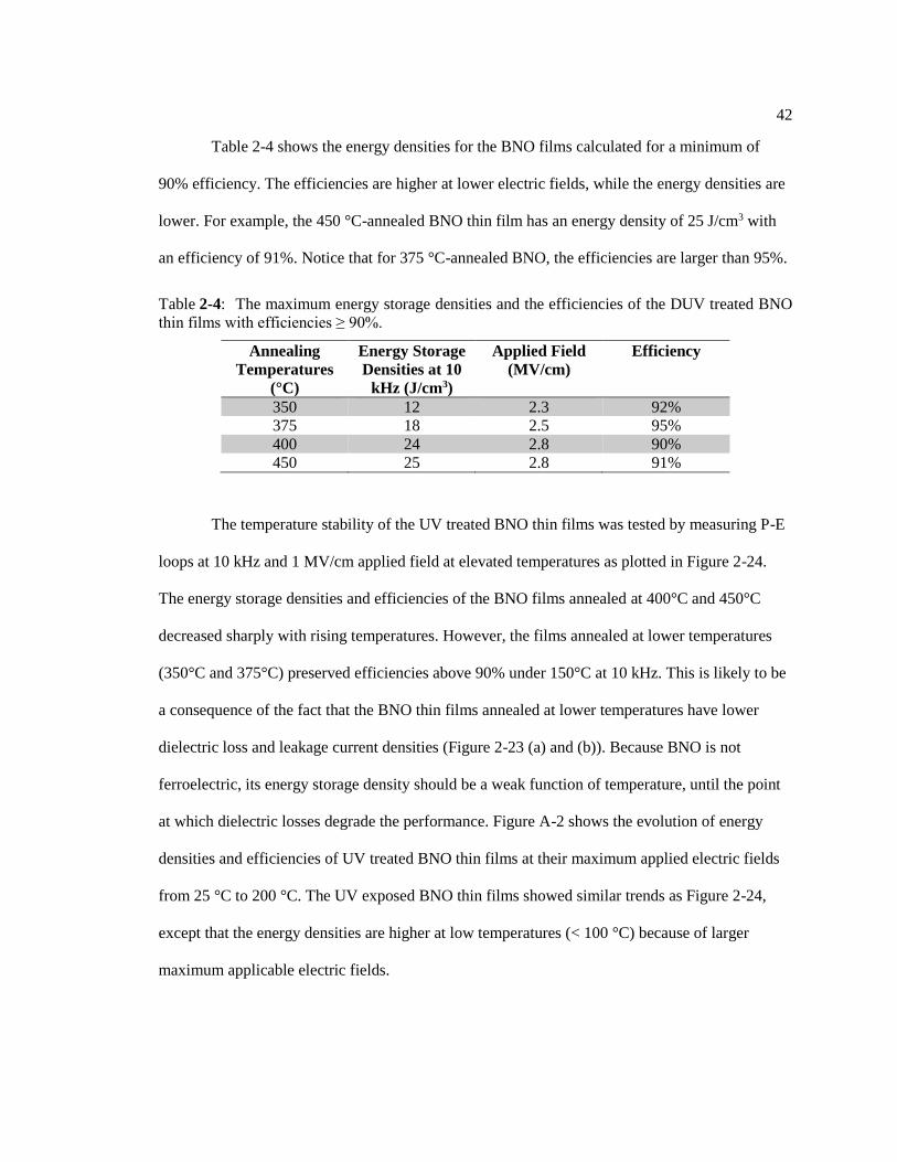
42
Table 2-4 shows the energy densities for the BNO films calculated for a minimum of
90% efficiency. The efficiencies are higher at lower electric fields, while the energy densities are
lower. For example, the 450 °C-annealed BNO thin film has an energy density of 25 J/cm3 with
an efficiency of 91%. Notice that for 375 °C-annealed BNO, the efficiencies are larger than 95%.
The temperature stability of the UV treated BNO thin films was tested by measuring P-E
loops at 10 kHz and 1 MV/cm applied field at elevated temperatures as plotted in Figure 2-24.
The energy storage densities and efficiencies of the BNO films annealed at 400°C and 450°C
decreased sharply with rising temperatures. However, the films annealed at lower temperatures
(350°C and 375°C) preserved efficiencies above 90% under 150°C at 10 kHz. This is likely to be
a consequence of the fact that the BNO thin films annealed at lower temperatures have lower
dielectric loss and leakage current densities (Figure 2-23 (a) and (b)). Because BNO is not
ferroelectric, its energy storage density should be a weak function of temperature, until the point
at which dielectric losses degrade the performance. Figure A-2 shows the evolution of energy
densities and efficiencies of UV treated BNO thin films at their maximum applied electric fields
from 25 °C to 200 °C. The UV exposed BNO thin films showed similar trends as Figure 2-24,
except that the energy densities are higher at low temperatures (< 100 °C) because of larger
maximum applicable electric fields.
Table 2-4: The maximum energy storage densities and the efficiencies of the DUV treated BNO
thin films with efficiencies ≥ 90%.
Annealing
Temperatures
(°C)
Energy Storage
Densities at 10
kHz (J/cm3)
Applied Field
(MV/cm)
Efficiency
350 12 2.3 92%
375 18 2.5 95%
400 24 2.8 90%
450 25 2.8 91%
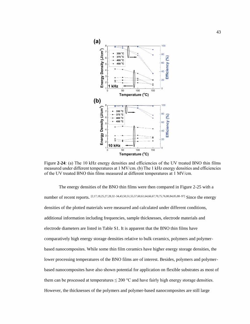
43
The energy densities of the BNO thin films were then compared in Figure 2-25 with a
number of recent reports. [2,17,18,25,27,28,32–34,43,50,51,55,57,60,61,64,66,67,70,75,76,80,84,85,88–97] Since the energy
densities of the plotted materials were measured and calculated under different conditions,
additional information including frequencies, sample thicknesses, electrode materials and
electrode diameters are listed in Table S1. It is apparent that the BNO thin films have
comparatively high energy storage densities relative to bulk ceramics, polymers and polymer-
based nanocomposites. While some thin film ceramics have higher energy storage densities, the
lower processing temperatures of the BNO films are of interest. Besides, polymers and polymer-
based nanocomposites have also shown potential for application on flexible substrates as most of
them can be processed at temperatures ≤ 200 °C and have fairly high energy storage densities.
However, the thicknesses of the polymers and polymer-based nanocomposites are still large
Figure 2-24: (a) The 10 kHz energy densities and efficiencies of the UV treated BNO thin films
measured under different temperatures at 1 MV/cm. (b) The 1 kHz energy densities and efficiencies
of the UV treated BNO thin films measured at different temperatures at 1 MV/cm.
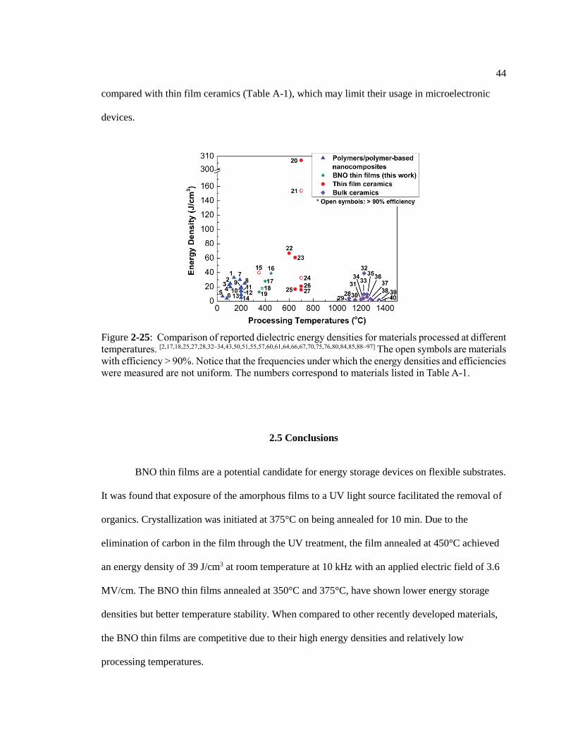
44
compared with thin film ceramics (Table A-1), which may limit their usage in microelectronic
devices.
2.5 Conclusions
BNO thin films are a potential candidate for energy storage devices on flexible substrates.
It was found that exposure of the amorphous films to a UV light source facilitated the removal of
organics. Crystallization was initiated at 375°C on being annealed for 10 min. Due to the
elimination of carbon in the film through the UV treatment, the film annealed at 450°C achieved
an energy density of 39 J/cm3 at room temperature at 10 kHz with an applied electric field of 3.6
MV/cm. The BNO thin films annealed at 350°C and 375°C, have shown lower energy storage
densities but better temperature stability. When compared to other recently developed materials,
the BNO thin films are competitive due to their high energy densities and relatively low
processing temperatures.
Figure 2-25: Comparison of reported dielectric energy densities for materials processed at different
temperatures. [2,17,18,25,27,28,32–34,43,50,51,55,57,60,61,64,66,67,70,75,76,80,84,85,88–97] The open symbols are materials
with efficiency > 90%. Notice that the frequencies under which the energy densities and efficiencies
were measured are not uniform. The numbers correspond to materials listed in Table A-1.
45
References
[1] Zhao, L.; Zhou, Z. L.; Guo, Z.; Gibson, G.; Brug, J. A.; Lam, S.; Pei, J.; Mao, S. S.
Development of Semi-Interpenetrating Polymer Networks and Quantum Dots–Polymer
Nanocomposites for Low-Cost, Flexible OLED Display Application. J. Mater. Res. 2012, 27 (4),
639–652.
[2] Michael-Sapia, E. K.; Li, H. U.; Jackson, T. N.; Trolier-McKinstry, S. Nanocomposite
Bismuth Zinc Niobate Tantalate for Flexible Energy Storage Applications. J. Appl. Phys. 2015,
118 (23), 234102.
[3] Li, Q.; Chen, L.; Gadinski, M. R.; Zhang, S.; Zhang, G.; Li, H.; Haque, A.; Chen, L. Q.;
Jackson, T.; Wang, Q. Flexible High-Temperature Dielectric Materials from Polymer
Nanocomposites. Nature 2015, 523 (7562), 576–579.
[4] Wu, A.; Vilarinho, P. M.; Kingon, A. I. Ceramic Processing Strategies for Thick Films on
Copper Foils. Acta Mater. 2010, 58 (6), 2282–2290.
[5] Maria, J.; Cheek, K.; Streiffer, S.; Kim, S.; Dunn, G.; Kingon, A. Lead Zirconate Titanate
Thin Films on Base-Metal Foils: An Approach for Embedded High-Permittivity Passive
Components. J. Am. Ceram. Soc. 2001, 84 (10), 2436–2438.
[6] Nderson, W. A. BaTiO3 Thin Film Capacitors Deposited by r.f. Magnetron Sputtering. Thin
Solid Films. 1992, 209 (2), 230–239.
[7] Ren, W.; Trolier-McKinstry, S.; Randall, C. A.; Shrout, T. R. Bismuth Zinc Niobate
Pyrochlore Dielectric Thin Films for Capacitive Applications. J. Appl. Phys. 2001, 89 (1), 767–
774.
[8] Ko, R.; Carlen, M. Principles and Applications of Electrochemical Capacitors. Electrochim.
Acta. 2000, 24, 83–98.
46
[9] Moulson, A. J.; Herbert, J. M. Electroceramics: Materials, Properties, Applications, 2nd ed.;
John Wiley & Sons, Ltd., 2003.
[10] Wang, D.; Clark, M. B.; Trolier-McKinstry, S. Bismuth Niobate Thin Films for Dielectric
Energy Storage Applications. J. Am. Ceram. Soc. 2018, 101 (8), 3443–3451.
[11] Uchino, K.; Hirose, S. Loss Mechanisms in Piezoelectrics: How to Measure Different Losses
Separately. IEEE Trans. Ultrason. Ferroelectr. Freq. Control 2001, 48 (1), 307–321.
[12] O’Dwyer, J. J. Theory of Dielectric Breakdown in Solids. Solid State Sci. 1969, 116 (2),
239–242.
[13] Michael, E. K. Bismuth Pyrochlore-Based Thin Films for Dielectric Energy Storage, Ph.D.
thesis in Materials Science and Engineering, Pennsylvania State University, 2015.
[14] Sherrit, S. Analytical Model for the Strain-Field and Polarization-Field Hysteresis Curves for
Ferroic Materials. Proc. SPIE 2009, 6526 (8), 1–11.
[15] Bokov, A. A.; Ye, Z. Recent Progress in Relaxor Ferroelectrics with Perovskite Structure. J.
Mater. Sci. 2006, 41, 31–52.
[16] Kittel, C. Theory of Antiferroelectric Crystals. Phys. Rev. 1950, 82 (5), 729–732.
[17] Zhou, X.; Chu, B.; Neese, B.; Lin, M.; Zhang, Q. M. Electrical Energy Density and
Discharge Characteristics of a Poly(Vinylidene Fluoride-Chlorotrifluoroethylene) Copolymer.
IEEE Trans. Dielectr. Electr. Insul. 2007, 14 (5), 1133–1138.
[18] Tomer, V.; Manias, E.; Randall, C. A. High Field Properties and Energy Storage in
Nanocomposite Dielectrics of Poly(Vinylidene Fluoride-Hexafluoropropylene). J. Appl. Phys.
2011, 110 (4), 044107.
[19] Newnham, R. E.; Trolier-McKinstry, S. Materials Engineering: Bonding, Structure, and
Structure-Property Relationships; Cambridge University Press, 2017.
[20] Rabuffi, M.; Picci, G. Status Quo and Future Prospects for Metallized Polypropylene Energy
Storage Capacitors. IEEE Trans. Plasma Sci. 2002, 30 (5), 1939–1942.
47
[21] Huan, T. D.; Boggs, S.; Teyssedre, G.; Laurent, C.; Cakmak, M.; Kumar, S.; Ramprasad, R.
Advanced Polymeric Dielectrics for High Energy Density Applications. Prog. Mater. Sci. 2016,
83, 236–269.
[22] Shigeyoshi, N.; Takashi, M.; Hirokazu, S.; Morihiko, H.; Katsuji, K.; Kazuo, I. Impregnated
Capacitor. U. S. Patent 4131931 A, 1978.
[23] Yoshinori, M.; Tadakazu, I.; Fumio, J. Biaxially Oriented Polyproplyene Film. U. S. Patent
7872085 B2, 2011.
[24] Wan, C.; Bowen, C. R. Multiscale-Structuring of Polyvinylidene Fluoride for Energy
Harvesting: The Impact of Molecular-, Micro- and Macro-Structure. J. Mater. Chem. A 2017, 5,
3091–3128.
[25] Li, W.; Meng, Q.; Zheng, Y.; Zhang, Z.; Xia, W.; Xu, Z. Electric Energy Storage Properties
of Poly(Vinylidene Fluoride). Appl. Phys. Lett. 2010, 96 (19), 192905.
[26] Chu, B. A Dielectric Polymer with High Electric Energy Density and Fast Discharge Speed.
Science 2006, 313 (5785), 334–336.
[27] Zhou, X.; Zhao, X.; Suo, Z.; Zou, C.; Runt, J.; Liu, S.; Zhang, S.; Zhang, Q. M. Electrical
Breakdown and Ultrahigh Electrical Energy Density in Poly(Vinylidene Fluoride-
Hexafluoropropylene) Copolymer. Appl. Phys. Lett. 2009, 94 (16), 162901.
[28] Rahimabady, M.; Yao, K.; Arabnejad, S.; Lu, L.; Shim, V. P. W. Intermolecular Interactions
and High Dielectric Energy Storage Density in Poly (Vinylidene Fluoride-
Hexafluoropropylene)/Poly(Vinylidene Fluoride) Blend Thin Films. Appl. Phys. Lett. 2012, 100
(25), 252907.
[29] Cheng, Z.; Lin, M.; Wu, S.; Thakur, Y.; Zhou, Y.; Jeong, D.; Shen, Q.; Zhang, Q. M.
Aromatic Poly(Arylene Ether Urea) with High Dipole Moment for High Thermal Stability and
High Energy Density Capacitors. Appl. Phys. Lett. 2015, 106 (20), 202902.
48
[30] Zhang, Z.; Wang, D. H.; Litt, M. H.; Tan, L. S.; Zhu, L. High Temperature and High Energy
Density Dipolar Glass Polymers Based on Sulfonylated Poly(2,6-Dimethyl-1,4-Phenylene
Oxide). Angew. Chemie - Int. Ed. 2017, 57 (6), 1528–1531.
[31] Wang, C. C.; Pilania, G.; Boggs, S. A.; Kumar, S.; Breneman, C.; Ramprasad, R.
Computational Strategies for Polymer Dielectrics Design. Polymer (Guildf). 2014, 55 (4), 979–
988.
[32] Bi, M.; Hao, Y.; Zhang, J.; Lei, M.; Bi, K. Particle Size Effect of BaTiO3 Nanofillers on the
Energy Storage Performance of Polymer Nanocomposites. Nanoscale 2017, 9 (42), 16386–16395.
[33] Zhang, X.; Shen, Y.; Zhang, Q.; Gu, L.; Hu, Y.; Du, J.; Lin, Y.; Nan, C. W. Ultrahigh
Energy Density of Polymer Nanocomposites Containing BaTiO3@TiO2 Nanofibers by Atomic-
Scale Interface Engineering. Adv. Mater. 2015, 27 (5), 819–824.
[34] Michael, E. K.; Trolier-McKinstry, S. Bismuth Pyrochlore Thin Films for Dielectric Energy
Storage. J. Appl. Phys. 2015, 118 (5), 054101.
[35] Dang, Z. M.; Yuan, J. K.; Zha, J. W.; Zhou, T.; Li, S. T.; Hu, G. H. Fundamentals, Processes
and Applications of High-Permittivity Polymer−Matrix Composites. Prog. Mater. Sci. 2012, 57,
660–723.
[36] Maxwell-Garnett, J. C.; Larmor, J. Colours in Metal Glasses and in Metallic Films. Phil.
Trans. A 1904, 203, 385–420.
[37] Yamada, T.; Ueda, T.; Kitayama, T. Piezoelectricity of a High-Content Lead Zirconate
Titanate Polymer Composite. J. Appl. Phys. 1982, 53 (6), 4328–4332.
[38] Knott, E. F. Dielectric Constant of Plastic Foams. IEEE Trans. Antennas Propag. 1993, 41
(8), 1167–1171.
[39] Zhang, L.; Bass, P.; Cheng, Z. Y. Physical Aspects of 0-3 Dielectric Composites. J. Adv.
Dielectr. 2015, 5 (2), 1550012.
49
[40] Tanaka, T.; Kozako, M. Proposal of a Multi-Core Model for Polymer Nanocomposite
Dielectrics. IEEE Trans. Dielectr. Electr. Insul. 2005, 12 (4), 669–681.
[41] Shen, Z. H.; Wang, J. J.; Lin, Y.; Nan, C. W.; Chen, L. Q.; Shen, Y. High-Throughput
Phase-Field Design of High-Energy-Density Polymer Nanocomposites. Adv. Mater. 2018, 30 (2),
1–6.
[42] Varshneya, A.; Mauro, J. Fundamentals of Inorganic Glasses, 3rd ed.; Academic Press:
London, UK, 2019.
[43] Smith, N. J.; Rangarajan, B.; Lanagan, M. T.; Pantano, C. G. Alkali-Free Glass as a High
Energy Density Dielectric Material. Mater. Lett. 2009, 63 (15), 1245–1248.
[44] Manoharan, M. P.; Zou, C.; Furman, E.; Zhang, N.; Kushner, D. I. Flexible Glass for High
Temperature Energy Storage Capacitors. Energy Technol. Commun. 2013, 1, 313–318.
[45] Solomon, P. Breakdown in Silicon Oxide-A Review. J. Vac. Sci. Technol. 1977, 14, 1122–
1130.
[46] Tsurumi, T.; Adachi, H.; Kakemoto, H.; Wada, S.; Mizuno, Y.; Chazono, H.; Kishi, H.
Related Content Dielectric Properties of BaTiO3-Based Ceramics under High Electric Field. Jpn.
J. Appl. Phys. 2002, 41 (1), 6929–6933.
[47] Gai, Z.; Cheng, Z.; Wang, X.; Zhao, L.; Yin, N.; Abah, R.; Zhao, M.; Hong, F.; Yu, Z.; Dou,
S. A Colossal Dielectric Constant of an Amorphous TiO2:(Nb, In) Film with Low Loss
Fabrication at Room Temperature. J. Mater. Chem. C 2014, 2, 6790–6795.
[48] Hu, W.; Liu, Y.; Withers, R. L.; Frankcombe, T. J.; Norén, L.; Snashall, A.; Kitchin, M.;
Smith, P.; Gong, B.; Chen, H.; Schiemer, J.; Brink, F.; Wong-Leung, J. Electron-Pinned Defect-
Dipoles for High-Performance Colossal Permittivity Materials. Nat. Mater. 2013, 12 (9), 821–
826.
50
[49] Liu, Z.; Zhao, C.; Wu, J. Reduced Dielectric Loss in New Colossal Permittivity (Pr, Nb)TiO2
Ceramics by Suppressing Adverse Effects of Secondary Phases. Phys. Chem. Chem. Phys.
Commun. 2018, 20 (34), 21814–21821.
[50] Shay, D. P.; Podraza, N. J.; Donnelly, N. J.; Randall, C. A. High Energy Density, High
Temperature Capacitors Utilizing Mn-Doped 0.8CaTiO3-0.2CaHfO3 Ceramics. J. Am. Ceram.
Soc. 2012, 95 (4), 1348–1355.
[51] Su, X.; Riggs, B. C.; Tomozawa, M.; Nelson, J. K.; Chrisey, D. B. Preparation of
BaTiO3/Low Melting Glass Core–Shell Nanoparticles for Energy Storage Capacitor Applications.
J. Mater. Chem. A 2014, 2 (42), 18087–18096.
[52] Lin, Y.; Li, D.; Zhang, M.; Zhan, S.; Yang, Y.; Yang, H.; Yuan, Q. Excellent Energy-
Storage Properties Achieved in BaTiO3-Based Lead-Free Relaxor Ferroelectric Ceramics via
Domain Engineering on the Nanoscale. ACS Appl. Mater. Interfaces 2019.
[53] Yang, H.; Yan, F.; Lin, Y.; Wang, T.; Wang, F. High Energy Storage Density over a Broad
Temperature Range in Sodium Bismuth Titanate-Based Lead-Free Ceramics. Sci. Rep. 2017, 7
(1), 8726.
[54] Wang, C.; Yan, F.; Yang, H.; Lin, Y.; Wang, T. Dielectric and Ferroelectric Properties of
SrTiO3-Bi0.54Na0.46TiO3-BaTiO3 Lead-Free Ceramics for High Energy Storage Applications. J.
Alloys Compd. 2018, 749, 605–611.
[55] Yan, F.; Yang, H.; Lin, Y.; Wang, T. Dielectric and Ferroelectric Properties of SrTiO3–
Bi0.5Na0.5TiO3–BaAl0.5Nb0.5O3 Lead-Free Ceramics for High-Energy-Storage Applications. Inorg.
Chem. 2017, 56 (21), 13510–13516.
[56] Li, F.; Jiang, T.; Zhai, J.; Shen, B.; Zeng, H. Exploring Novel Bismuth-Based Materials for
Energy Storage Applications. J. Mater. Chem. C 2018, 6 (30), 7975–7981.
[57] Wang, T.; Jin, L.; Li, C.; Hu, Q.; Wei, X. Relaxor Ferroelectric BaTiO3-Bi(Mg2/3Nb1/3)O3
Ceramics for Energy Storage Application. J. Am. Ceram. Soc. 2015, 98 (2), 559–566.
51
[58] Zhao, N.; Fan, H.; Ning, L.; Ma, J.; Zhou, Y. Temperature-Stable Dielectric and Energy
Storage Properties of La(Ti0.5Mg0.5)O3-Doped (Bi0.5Na0.5)TiO3-(Sr0.7Bi0.2)TiO3 Lead-Free
Ceramics. J. Am. Ceram. Soc. 2018, 101 (12), 5578–5585.
[59] Lu, X.; Zhang, L.; Talebinezhad, H.; Tong, Y.; Cheng, Z. Y. Effects of CuO Additive on the
Dielectric Property and Energy-Storage Performance of BaTiO3-SiO2 Ceramic-Glass Composite.
Ceram. Int. 2018, 44 (14), 16977–16983.
[60] Sun, Z.; Li, L.; Yu, S.; Kang, X.; Chen, S. Energy Storage Properties and Relaxor Behavior
of Lead-Free Ba1−xSm2x/3Zr0.15Ti0.85O3 Ceramics. Dalt. Trans. 2017, 46 (41), 14341–14347.
[61] Wei, M.; Zhang, J.; Zhang, M.; Yao, Z.; Chen, H.; Yang, C. Relaxor Behavior of BaTiO3-
BiYO3 Perovskite Materials for High Energy Density Capacitors. Ceram. Int. 2017, 43 (6), 4768–
4774.
[62] Li, J.; Li, F.; Xu, Z.; Zhang, S. Multilayer Lead-Free Ceramic Capacitors with Ultrahigh
Energy Density and Efficiency. Adv. Mater. 2018, 1802155, 1–7.
[63] Alkathy, M. S.; James Raju, K. C. Enhancement of Dielectric Properties and Energy Storage
Density of Bismuth and Lithium Co-Substituted Strontium Titanate Ceramics. Ceram. Int. 2018,
44 (9), 10367–10375.
[64] Ogihara, H.; Randall, C. A.; Trolier-McKinstry, S. High-Energy Density Capacitors
Utilizing 0.7BaTiO3-0.3BiScO3 Ceramics. J. Am. Ceram. Soc. 2009, 92 (8), 1719–1724.
[65] Lee, H.; Kim, J. R.; Lanagan, M. J.; Trolier-McKinstry, S.; Randall, C. A. High-Energy
Density Dielectrics and Capacitors for Elevated Temperatures: Ca(Zr, Ti)O3. J. Am. Ceram. Soc.
2013, 96 (4), 1209–1213.
[66] Zhao, L.; Liu, Q.; Gao, J.; Zhang, S.; Li, J. F. Lead-Free Antiferroelectric Silver Niobate
Tantalate with High Energy Storage Performance. Adv. Mater. 2017, 29 (31), 1701824.
52
[67] Shao, T.; Du, H.; Ma, H.; Qu, S.; Wang, J.; Wang, J.; Wei, X.; Xu, Z. Potassium-Sodium
Niobate Based Lead-Free Ceramics: Novel Electrical Energy Storage Materials. J. Mater. Chem.
A 2017, 5 (2), 554–563.
[68] Gao, J.; Zhao, L.; Liu, Q.; Wang, X.; Zhang, S.; Li, J. F. Antiferroelectric-Ferroelectric
Phase Transition in Lead-Free AgNbO3 Ceramics for Energy Storage Applications. J. Am.
Ceram. Soc. 2018, 101, 5443–5450.
[69] Pu, Y.; Zhang, L.; Cui, Y.; Chen, M. High Energy Storage Density and Optical Transparency
of Microwave Sintered Homogeneous (Na0.5Bi0.5)(1-x)BaxTi(1-y)SnyO3 Ceramics. ACS Sustain.
Chem. Eng. 2018, 6 (5), 6102–6109.
[70] Kumar, N.; Ionin, A.; Ansell, T.; Kwon, S.; Hackenberger, W.; Cann, D. Multilayer Ceramic
Capacitors Based on Relaxor BaTiO3-Bi(Zn1/2Ti1/2)O3 for Temperature Stable and High Energy
Density Capacitor Applications. Appl. Phys. Lett. 2015, 106 (25), 252901.
[71] Funahashi, S.; Guo, J.; Guo, H.; Wang, K.; Baker, A. L.; Shiratsuyu, K.; Randall, C. A.
Demonstration of the Cold Sintering Process Study for the Densification and Grain Growth of
ZnO Ceramics. J. Am. Ceram. Soc. 2017, 100 (2), 546–553.
[72] Zhang, Y.; Cao, M.; Yao, Z.; Wang, Z.; Song, Z.; Ullah, A.; Hao, H.; Liu, H. Effects of
Silica Coating on the Microstructures and Energy Storage Properties of BaTiO3 Ceramics. Mater.
Res. Bull. 2015, 67, 70–76.
[73] Huang, X.; Hao, H.; Zhang, S.; Liu, H.; Zhang, W.; Xu, Q.; Cao, M. Structure and Dielectric
Properties of BaTiO3-BiYO3 Perovskite Solid Solutions. J. Am. Ceram. Soc. 2014, 97 (6), 1797–
1801.
[74] Yang, C. H.; Yao, Q.; Qian, J.; Han, Y. J.; Chen, J. Growth , Microstructure , Energy–
Storage and Dielectric Performances of Chemical–Solution NBT–Based Thin Films : Effect of
Sodium Nonstoichiometry. Ceram. Int. 2018, 44 (8), 9152–9158.
53
[75] Peng, B.; Zhang, Q.; Li, X.; Sun, T.; Fan, H.; Ke, S.; Ye, M.; Wang, Y.; Lu, W.; Niu, H.; et
al. Giant Electric Energy Density in Epitaxial Lead-Free Thin Films with Coexistence of
Ferroelectrics and Antiferroelectrics. Adv. Electron. Mater. 2015, 1 (5), 1500052.
[76] Zhang, L.; Liu, M.; Ren, W.; Zhou, Z.; Dong, G.; Zhang, Y.; Peng, B.; Hao, X.; Wang, C.;
Jiang, Z. D.; et al. ALD Preparation of High-k HfO2 Thin Films with Enhanced Energy Density
and Efficient Electrostatic Energy Storage. RSC Adv. 2017, 7 (14), 8388–8393.
[77] Liang, Z.; Liu, M.; Shen, L.; Lu, L.; Ma, C.; Lu, X.; Lou, X.; Jia, C. All-Inorganic Flexible
Embedded Thin-Film Capacitors for Dielectric Energy Storage with High Performance. ACS
Appl. Mater. Interfaces 2019, 11 (5), 5247–5255.
[78] Pan, H.; Li, F.; Liu, Y.; Zhang, Q.; Wang, M.; Lan, S.; Zheng, Y.; Ma, J.; Gu, L.; Shen, Y.;
et al. Ultrahigh–Energy Density Lead-Free Dielectric Films via Polymorphic Nanodomain
Design. Science. 2019, 365 (6453), 578–582.
[79] Hu, Z.; Ma, B.; Koritala, R. E.; Balachandran, U. Temperature-Dependent Energy Storage
Properties of Antiferroelectric Pb0.96La0.04Zr0.98Ti0.02O3 Thin Films. Appl. Phys. Lett. 2014, 104
(26), 263902.
[80] Hou, C.; Huang, W.; Zhao, W.; Zhang, D.; Yin, Y.; Li, X. Ultrahigh Energy Density in
SrTiO3 Film Capacitors. ACS Appl. Mater. Interfaces 2017, 9 (24), 20484–20490.
[81] Su, Z.; Yao, M.; Li, M.; Gao, W.; Li, Q.; Feng, Q.; Yao, X. A Novel and Simple
Aluminium/Sol–Gel-Derived Amorphous Aluminium Oxide Multilayer Film with High Energy
Density. J. Mater. Chem. C 2018, 6 (21), 5616–5623.
[82] Hou, Y.; Han, R.; Li, W.; Luo, L.; Fei, W. Significantly Enhanced Energy Storage
Performance in BiFeO3/BaTiO3/BiFeO3 Sandwich-Structured Films through Crystallinity
Regulation. Phys. Chem. Chem. Phys. 2018, 20 (34), 21917–21924.
54
[83] Zhang, T.; Li, W.; Hou, Y.; Yu, Y.; Song, R.; Cao, W.; Fei, W. High-Energy Storage
Density and Excellent Temperature Stability in Antiferroelectric/Ferroelectric Bilayer Thin Films.
J. Am. Ceram. Soc. 2017, 100 (7), 3080–3087.
[84] Zhang, G.; Zhu, D.; Zhang, X.; Zhang, L.; Yi, J.; Xie, B.; Zeng, Y.; Li, Q.; Wang, Q.; Jiang,
S. High-Energy Storage Performance of (Pb0.87Ba0.1La0.02)(Zr0.68Sn0.24Ti0.08)O3 Antiferroelectric
Ceramics Fabricated by the Hot-Press Sintering Method. J. Am. Ceram. Soc. 2015, 98 (4), 1175–
1181.
[85] Ahn, C. W.; Amarsanaa, G.; Won, S. S.; Chae, S. A.; Lee, D. S.; Kim, I. W. Antiferroelectric
Thin-Film Capacitors with High Energy-Storage Densities, Low Energy Losses, and Fast
Discharge Times. ACS Appl. Mater. Interfaces 2015, 7 (48), 26381–26386.
[86] Castro, A.; Aguado, E.; Rojo, J. M.; Herrero, P.; Enjalbert, R.; Galy, J. The New Oxygen-
Deficient Fluorite Bi3NbO7: Synthesis, Electrical Behavior and Structural Approach. Mater. Res.
Bull. 1998, 33 (1), 31–41.
[87] Bretos, I.; Jiménez, R.; Ricote, J.; Calzada, M. L. Low-Temperature Crystallization of
Solution-Derived Metal Oxide Thin Films Assisted by Chemical Processes. Chem. Soc. Rev.
2018, 47 (2), 291–308.
[88] Tang, H.; Sodano, H. A. Ultra High Energy Density Nanocomposite Capacitors with Fast
Discharge Using Ba0.2Sr0.8TiO3 Nanowires. Nano Lett. 2013, 13 (4), 1373–1379.
[89] Li, Q.; Zhang, G.; Liu, F.; Han, K.; Gadinski, M. R.; Xiong, C.; Wang, Q. Solution-
Processed Ferroelectric Terpolymer Nanocomposites with High Breakdown Strength and Energy
Density Utilizing Boron Nitride Nanosheets. Energy Environ. Sci. 2015, 8 (3), 922–931.
[90] Puli, V. S.; Ejaz, M.; Elupula, R.; Kothakonda, M.; Adireddy, S.; Katiyar, R. S.; Grayson, S.
M.; Chrisey, D. B. Core-Shell like Structured Barium Zirconium Titanate-Barium Calcium
Titanate-Poly(Methyl Methacrylate) Nanocomposites for Dielectric Energy Storage Capacitors.
Polymer. 2016, 105, 35–42.
55
[91] Wang, G.; Huang, Y.; Wang, Y.; Jiang, P.; Huang, X. Substantial Enhancement of Energy
Storage Capability in Polymer Nanocomposites by Encapsulation of BaTiO3 NWs with Variable
Shell Thickness. Phys. Chem. Chem. Phys. 2017, 19 (31), 21058–21068.
[92] Pan, Z. B.; Yao, L. M.; Zhai, J. W.; Liu, S. H.; Yang, K.; Wang, H. T.; Liu, J. H. Fast
Discharge and High Energy Density of Nanocomposite Capacitors Using Ba0.6Sr0.4TiO3
Nanofibers. Ceram. Int. 2016, 42 (13), 14667–14674.
[93] Wang, J.; Liu, S.; Wang, J.; Hao, H.; Zhao, L.; Zhai, J. Improving Dielectric Properties and
Energy Storage Performance of Poly(Vinylidene Fluoride) Nanocomposite by Surface-Modified
SrTiO3 Nanoparticles. J. Alloys Compd. 2017, 726, 587–592.
[94] Wang, X.; Hao, X.; Zhang, Q.; An, S.; Chou, X. Energy-Storage Performance and
Pyroelectric Energy Harvesting Effect of PNZST Antiferroelectric Thin Films. J. Mater. Sci.
Mater. Electron. 2017, 28 (2), 1438–1448.
[95] Zhang, Y. L.; Li, W. L.; Cao, W. P.; Zhang, T. D.; Bai, T. R. G. L.; Yu, Y.; Hou, Y. F.;
Feng, Y.; Fei, W. D. Enhanced Energy-Storage Performance of 0.94NBT-0.06BT Thin Films
Induced by a Pb0.8La0.1Ca0.1Ti0.975O3 Seed Layer. Ceram. Int. 2016, 42, 14788–14792.
[96] Dong, W. D.; Carlos Valadez, J.; Gallagher, J. A.; Jo, H. R.; Sahul, R.; Hackenberger, W.;
Lynch, C. S. Pressure, Temperature, and Electric Field Dependence of Phase Transformations in
Niobium Modified 95/5 Lead Zirconate Titanate. J. Appl. Phys. 2015, 117 (24), 244104.
[97] Rahimabady, M.; Qun Xu, L.; Arabnejad, S.; Yao, K.; Lu, L.; Shim, V. P. W.; Gee Neoh, K.;
Kang, E. T. Poly(Vinylidene Fluoride-Co-Hexafluoropropylene)-Graft-Poly(Dopamine
Methacrylamide) Copolymers: A Nonlinear Dielectric Material for High Energy Density Storage.
Appl. Phys. Lett. 2013, 103 (26), 262904.
* Part of this chapter is reproduced from D. Wang, H. Guo, C. S. Morandi, C. A. Randall, and S.
Trolier-McKinstry “Cold Sintering and Electrical Characterization of Lead Zirconate Titanate
Piezoelectric Ceramics.” APL Materials 6, 016101 (2018).
Chapter 3
The Cold Sintering Process and Electrical Characterizations of Lead
Zirconate Titanate Ceramics
3.1 Introduction
Electro-ceramic materials are widely utilized in commercial electronics. For example,
multilayer ceramic capacitors [1] and semiconducting varistors [2] are used in computers,
cellphones and surge protection circuits. Thermoelectric [3] and piezoelectric sensors/actuators [4]
incorporated in health monitors help save lives. Perovskite solar cells [5] and lithium-based
battery electrodes [6] generate and store local power as well as renewable energy for next-
generation vehicles and accommodations.
In every circumstance, the density of an electro-ceramic material is critical to its
performance. For example, pores in a capacitor cause lower dielectric breakdown strength,
reduced effective relative permittivities, and decreased device lifetimes; cracks in piezoelectric
sensors cause a significant drop in sensitivity, etc. Consequently, a relative density >95% is
desired for most electroceramics; this is typically difficult to realize at low temperatures.
Lead zirconate titanate (PZT) is a piezoelectric material widely employed in ultrasound
transducers [7], precise positioning actuators, [8] sensors, and energy harvesters [9]. Typically, PZT
requires a sintering temperature > 1200 °C [10]. Therefore, a number of methods have been
explored to reduce the maximum processing temperature of PZT to 700˚C-1000˚C, including hot
pressing [11,12], liquid phase sintering [13–15], microwave sintering [16] and field assisted sintering
(spark plasma sintering) [17].
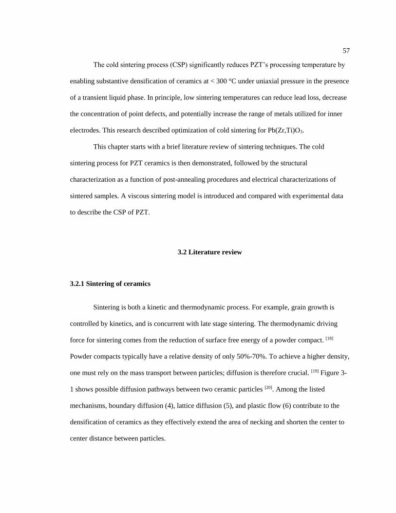
57
The cold sintering process (CSP) significantly reduces PZT’s processing temperature by
enabling substantive densification of ceramics at < 300 °C under uniaxial pressure in the presence
of a transient liquid phase. In principle, low sintering temperatures can reduce lead loss, decrease
the concentration of point defects, and potentially increase the range of metals utilized for inner
electrodes. This research described optimization of cold sintering for Pb(Zr,Ti)O3.
This chapter starts with a brief literature review of sintering techniques. The cold
sintering process for PZT ceramics is then demonstrated, followed by the structural
characterization as a function of post-annealing procedures and electrical characterizations of
sintered samples. A viscous sintering model is introduced and compared with experimental data
to describe the CSP of PZT.
3.2 Literature review
3.2.1 Sintering of ceramics
Sintering is both a kinetic and thermodynamic process. For example, grain growth is
controlled by kinetics, and is concurrent with late stage sintering. The thermodynamic driving
force for sintering comes from the reduction of surface free energy of a powder compact. [18]
Powder compacts typically have a relative density of only 50%-70%. To achieve a higher density,
one must rely on the mass transport between particles; diffusion is therefore crucial. [19] Figure 3-
1 shows possible diffusion pathways between two ceramic particles [20]. Among the listed
mechanisms, boundary diffusion (4), lattice diffusion (5), and plastic flow (6) contribute to the
densification of ceramics as they effectively extend the area of necking and shorten the center to
center distance between particles.
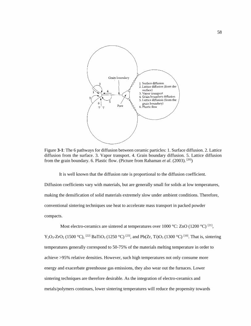
58
It is well known that the diffusion rate is proportional to the diffusion coefficient.
Diffusion coefficients vary with materials, but are generally small for solids at low temperatures,
making the densification of solid materials extremely slow under ambient conditions. Therefore,
conventional sintering techniques use heat to accelerate mass transport in packed powder
compacts.
Most electro-ceramics are sintered at temperatures over 1000 °C: ZnO (1200 °C) [21],
Y2O3-ZrO2 (1500 °C), [22] BaTiO3 (1250 °C) [23], and Pb(Zr, Ti)O3 (1300 °C) [10]. That is, sintering
temperatures generally correspond to 50-75% of the materials melting temperature in order to
achieve >95% relative densities. However, such high temperatures not only consume more
energy and exacerbate greenhouse gas emissions, they also wear out the furnaces. Lower
sintering techniques are therefore desirable. As the integration of electro-ceramics and
metals/polymers continues, lower sintering temperatures will reduce the propensity towards
Figure 3-1: The 6 pathways for diffusion between ceramic particles: 1. Surface diffusion. 2. Lattice
diffusion from the surface. 3. Vapor transport. 4. Grain boundary diffusion. 5. Lattice diffusion
from the grain boundary. 6. Plastic flow. (Picture from Rahaman et al. (2003). [20])
59
stress- or reaction- induced delaminate, and reduce the thermal expansion coefficient mismatch-
induced strains.
Several methods to reduce sintering temperature (or at least reduce the thermal energy
input during sintering) have been studied, including hot pressing (HP), liquid phase sintering
(LPS), microwave/millimeter wave sintering (MWS), flash sintering (FS), and a combinations of
these techniques, such as field assisted sintering technique (FAST, or spark plasma sintering
(SPS)), liquid-phase-assisted HP, liquid-phase-assisted FAST, and the cold sintering process
(CSP). All these techniques have utilized at least one of these three physical approaches:
I: Altering the form of energy delivered to the system (Ex. HP).
II: Manipulating the efficiency of energy delivered to the system (Ex. MWS and FS).
III: Adding a highly diffusive transport agent into the system (Ex. LPS).
General sintering techniques, including the low temperature sintering techniques
mentioned above, will be introduced in the following sections.
3.2.2 Solid state sintering (SSS)
Solid state sintering uses only heat to increase both grain boundary and lattice diffusion,
so as to achieve a high density. SSS can be divided into 3 stages: initial stage, intermediate stage
and final stage. Figure 3-2 shows the microstructural evolution of ceramic particles in these
different stages [24].
60
The initial stage of sintering is characterized by the formation of “necks” between
particles as the ceramic compacts start to coalesce. At this state, the relative density of a ceramic
compact is normally < 65%. Then, during the intermediate stage, as diffusion expands the
necking area, ceramic particles develop a tetrakaidecahedron morphology. Meanwhile, the pores
shrink into inter-connected narrow channels on the edge of the grains. These channels begin to
disappear at a relative density above 92%, known as the final stage, resulting in isolated pores and
closed triple points.
For the intermediate and the final stages of sintering, there are mathematical models
describing the density evolution. These were developed by Coble et al.[24] by solving self-
diffusion equations under the assumption that the grains are uniform in size, with the exact shapes
depicted in Figure (c) and (d) respectively for the intermediate and the final stage of sintering.
For the intermediate stage:
Figure 3-2: Illustration of morphology change in ceramic grains (a) before sintering, (b) at the
initial stage of sintering when necks begin to form, (c) during the intermediate stage of sintering
when grains turn into tetrakaidecahedrons with inter-connected pores, and (d) at final stage during
which the channels along the grain edge close up and pores are isolated. (Figure adopted from
Coble et al. (1961). [24])
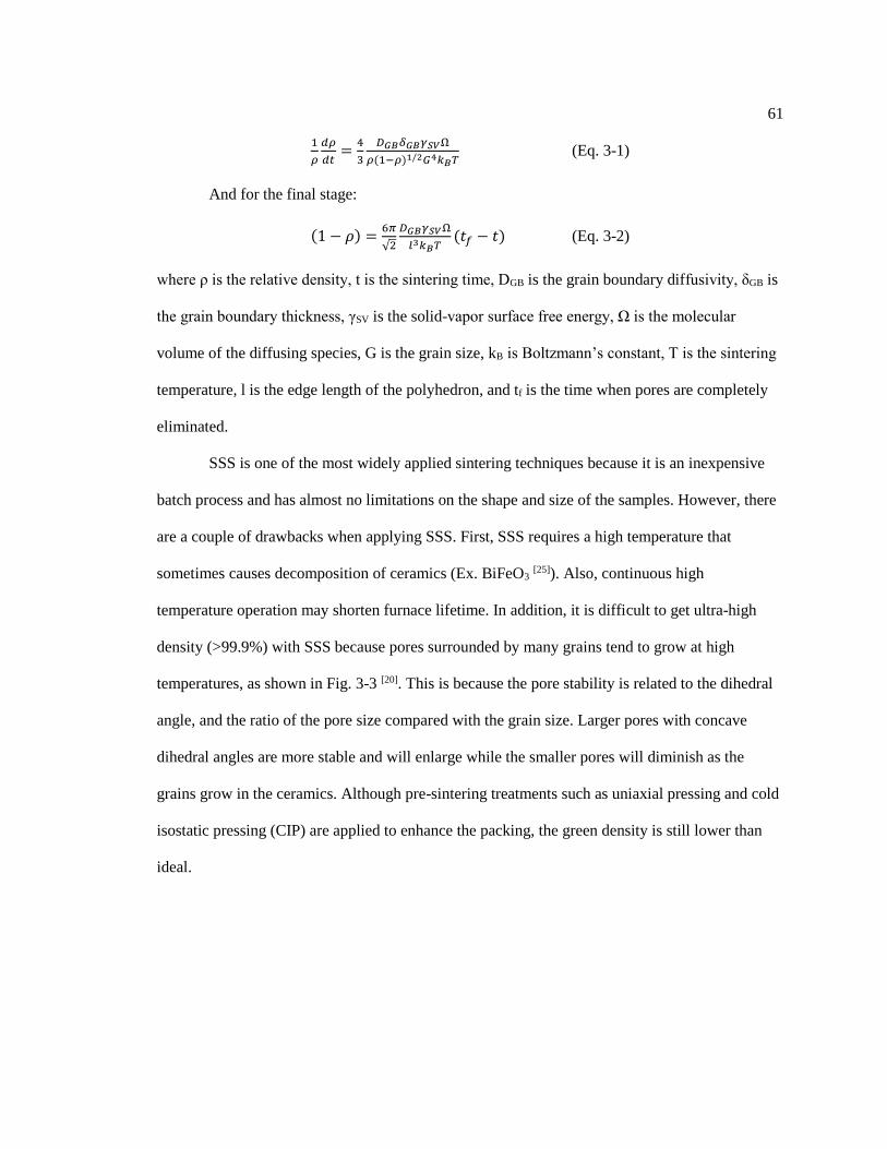
61
1
𝜌
𝑑𝜌
𝑑𝑡=
4
3
𝐷𝐺𝐵𝛿𝐺𝐵𝛾𝑆𝑉Ω
𝜌(1−𝜌)1/2𝐺4𝑘𝐵𝑇 (Eq. 3-1)
And for the final stage:
(1 − 𝜌) =6𝜋
√2
𝐷𝐺𝐵𝛾𝑆𝑉Ω
𝑙3𝑘𝐵𝑇(𝑡𝑓 − 𝑡) (Eq. 3-2)
where ρ is the relative density, t is the sintering time, DGB is the grain boundary diffusivity, δGB is
the grain boundary thickness, γSV is the solid-vapor surface free energy, Ω is the molecular
volume of the diffusing species, G is the grain size, kB is Boltzmann’s constant, T is the sintering
temperature, l is the edge length of the polyhedron, and tf is the time when pores are completely
eliminated.
SSS is one of the most widely applied sintering techniques because it is an inexpensive
batch process and has almost no limitations on the shape and size of the samples. However, there
are a couple of drawbacks when applying SSS. First, SSS requires a high temperature that
sometimes causes decomposition of ceramics (Ex. BiFeO3 [25]). Also, continuous high
temperature operation may shorten furnace lifetime. In addition, it is difficult to get ultra-high
density (>99.9%) with SSS because pores surrounded by many grains tend to grow at high
temperatures, as shown in Fig. 3-3 [20]. This is because the pore stability is related to the dihedral
angle, and the ratio of the pore size compared with the grain size. Larger pores with concave
dihedral angles are more stable and will enlarge while the smaller pores will diminish as the
grains grow in the ceramics. Although pre-sintering treatments such as uniaxial pressing and cold
isostatic pressing (CIP) are applied to enhance the packing, the green density is still lower than
ideal.
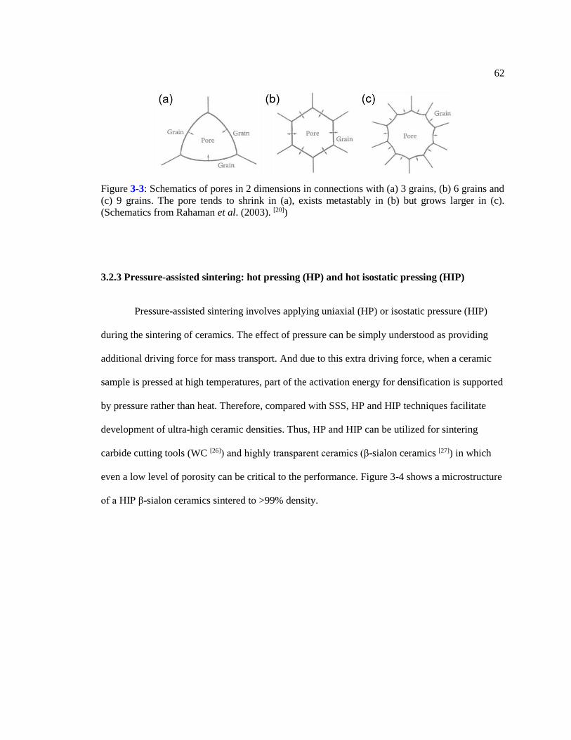
62
3.2.3 Pressure-assisted sintering: hot pressing (HP) and hot isostatic pressing (HIP)
Pressure-assisted sintering involves applying uniaxial (HP) or isostatic pressure (HIP)
during the sintering of ceramics. The effect of pressure can be simply understood as providing
additional driving force for mass transport. And due to this extra driving force, when a ceramic
sample is pressed at high temperatures, part of the activation energy for densification is supported
by pressure rather than heat. Therefore, compared with SSS, HP and HIP techniques facilitate
development of ultra-high ceramic densities. Thus, HP and HIP can be utilized for sintering
carbide cutting tools (WC [26]) and highly transparent ceramics (β-sialon ceramics [27]) in which
even a low level of porosity can be critical to the performance. Figure 3-4 shows a microstructure
of a HIP β-sialon ceramics sintered to >99% density.
Figure 3-3: Schematics of pores in 2 dimensions in connections with (a) 3 grains, (b) 6 grains and
(c) 9 grains. The pore tends to shrink in (a), exists metastably in (b) but grows larger in (c).
(Schematics from Rahaman et al. (2003). [20])
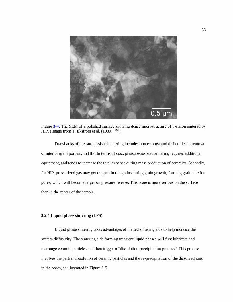
63
Drawbacks of pressure-assisted sintering includes process cost and difficulties in removal
of interior grain porosity in HIP. In terms of cost, pressure-assisted sintering requires additional
equipment, and tends to increase the total expense during mass production of ceramics. Secondly,
for HIP, pressurized gas may get trapped in the grains during grain growth, forming grain interior
pores, which will become larger on pressure release. This issue is more serious on the surface
than in the center of the sample.
3.2.4 Liquid phase sintering (LPS)
Liquid phase sintering takes advantages of melted sintering aids to help increase the
system diffusivity. The sintering aids forming transient liquid phases will first lubricate and
rearrange ceramic particles and then trigger a “dissolution-precipitation process.” This process
involves the partial dissolution of ceramic particles and the re-precipitation of the dissolved ions
in the pores, as illustrated in Figure 3-5.
Figure 3-4: The SEM of a polished surface showing dense microstructure of β-sialon sintered by
HIP. (Image from T. Ekström et al. (1989). [27])
64
Kwon et al. [28] studied the governing kinetics of LPS. The sintering rate is a function of
surface diffusion and interface reactions and can be described by the following equations:
For surface diffusion:
𝑑(Δ𝜌
𝜌)
𝑑𝑡=
𝐴𝛿𝐷𝑙𝐶0𝛾𝑙𝑣Ω
𝑘𝐵𝑇𝑟𝑠−4 (Eq. 3-3)
𝑑(Δ𝜌
𝜌)
𝑑𝑡=
𝐵𝐾𝐷𝑙𝐶0𝛾𝑙𝑣Ω
𝑘𝐵𝑇𝑟𝑠
−2 (Eq. 3-4)
in which ρ and t are relative density and sintering time respectively, A and B are geometrical
factors, δ is the thickness of the liquid film, Dl is the liquid phase diffusivity, C0 is the
concentration of the solute at equilibrium, γlv is the liquid-vapor surface tension, Ω is the
molecular volume of the dissolved species, kB is Boltzmann’s constant, T is the sintering
temperature, rs is the particle radius, and K is the reaction constant at the liquid-solid interface.
Figure 3-5: A schematic of the LPS at different stages. The initial compact consists of solid ceramic
powder and additive sintering aid. The sintering aid melts at elevated temperature and lubricates
the ceramic powder, resulting in particle rearrangement. Later on, as the dissolution-precipitation
process proceeds, densification and grain growth take place and the sample is sintered. (Figure
adopted from O. H. Kwon et al.) [28]
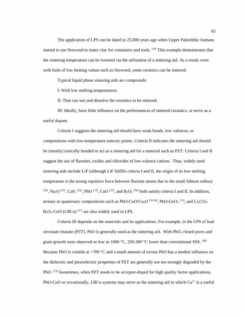
65
The application of LPS can be dated to 25,000 years ago when Upper Paleolithic humans
started to use firewood to sinter clay for containers and tools. [29] This example demonstrates that
the sintering temperature can be lowered via the utilization of a sintering aid. As a result, even
with fuels of low heating values such as firewood, some ceramics can be sintered.
Typical liquid phase sintering aids are compounds:
I: With low melting temperatures;
II: That can wet and dissolve the ceramics to be sintered;
III: Ideally, have little influence on the performances of sintered ceramics, or serve as a
useful dopant.
Criteria I suggests the sintering aid should have weak bonds, low valences, or
compositions with low-temperature eutectic points. Criteria II indicates the sintering aid should
be (mostly) ionically bonded to act as a sintering aid for a material such as PZT. Criteria I and II
suggest the use of fluorites, oxides and chlorides of low-valence cations. Thus, widely used
sintering aids include LiF (although LiF fulfills criteria I and II, the origin of its low melting
temperature is the strong repulsive force between fluorine atoms due to the small lithium radius)
[30], Na2O [31], CaF2 [32], PbO [13], CuO [33], and B2O3 [34] both satisfy criteria I and II. In addition,
ternary or quaternary compositions such as PbO-CuO/Cu2O [35,36], PbO-GeO2 [15], and Li2CO3-
B2O3-CuO (LBCu) [37] are also widely used in LPS.
Criteria III depends on the materials and its applications. For example, in the LPS of lead
zirconate titanate (PZT), PbO is generally used as the sintering aid. With PbO, closed pores and
grain growth were observed as low as 1000 °C, 250-300 °C lower than conventional SSS. [38]
Because PbO is volatile at >700 °C and a small amount of excess PbO has a modest influence on
the dielectric and piezoelectric properties of PZT are generally not too strongly degraded by the
PbO. [13] Sometimes, when PZT needs to be acceptor-doped for high quality factor applications,
PbO-CuO or occasionally, LBCu systems may serve as the sintering aid in which Cu2+ is a useful
66
dopant [35,37]. Other sintering aids, such as PbO-GeO2 and LiBiO2 result in mediocre piezoelectric
properties due to Ge/Li-contained grain boundaries; hence these are not as useful as other
sintering aids, even though sintering temperatures < 800 °C were claimed. [14,15]
The presence of a transient liquid phase is a “double-edged sword”. On one hand, the
liquid phase increases the diffusivity significantly, resulting in densification at a lower
temperature; on the other hand, it facilitates grain interior pores formation caused by rapid grain
growth and, most of the time, unwanted secondary phases formed by residual sintering aids.
3.2.5 Viscous sintering
Viscous sintering is widely employed in the sintering of glass materials; in this process,
plastic flow fills the pores. During sintering, glasses gradually become less viscous as the
temperature increases. Commercially, glass materials are sintered and processed between their
softening points (viscosity = 107.65 Poise, where the glass materials start to “deform under its own
weight” [39]) and working points (viscosity = 104 Poise, below which the glass can be worked on a
machine [39]). This interval is called the “working range”. [39] For alkali-lead glasses and soda-lime
glasses, the working range is between 600-1000 °C while for borosilicate glasses and
aluminosilicate glasses the working range increases to 800-1200 °C. [39] Notice that these
temperatures are slightly lower than typical sintering temperatures for ceramics.
Viscous sintering can also be treated as a special case of LPS when the liquid phase is the
main component to be sintered. For a system containing viscous phase and hard inclusions, if the
liquid phase volume fraction is below 40%, it is considered to be LPS. Otherwise the process is
treated as viscous sintering. [20]
67
3.2.6 Electromagnetic field-assisted sintering
The motivation for electromagnetic field-assisted sintering is to enhance the efficiency of
the energy input during sintering. It is achieved by applying high currents or electromagnetic
waves that directly heats the samples instead of heating the rest of the chamber. Due to the
smaller heating volume than conventional sintering, electromagnetic field-assisted sintering
techniques are characterized by ultra-fast heating and cooling rates, leading to fine grain sizes [40].
This enables the production of cutting tools and abrasives with high hardness, such as tungsten
carbide [41] and alumina [42].
Electromagnetic field-assisted sintering encompasses two techniques: microwave/
millimeter-wave sintering (MWS) and electric current-assisted sintering (ECAS). MWS operates
similar to a microwave oven in that the ceramic samples are heated by the electromagnetic
radiation. ECAS is sometimes considered as a combination of two similar sintering techniques:
field-assisted sintering technique (FAST) and flash sintering (FS), both of which uses large
currents to generate significant Joule heating that densifies the ceramics. The only difference is in
FS, a ceramic green body is heated to an “onset temperature” at which the electrical conductivity
is significantly increased, resulting in complete sintering in a “flash” [43].
Depending on their mechanisms, one of the drawbacks of electromagnetic field-assisted
sintering techniques is the need for absorption of electromagnetic fields by the samples. This has
been accommodated by either utilizing a susceptor that resonates/conducts well with the applied
fields or by adding a small amount of dopants or phases that increase the absorption. [44,45]
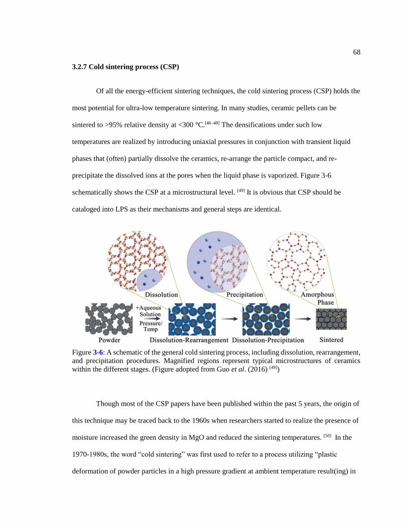
68
3.2.7 Cold sintering process (CSP)
Of all the energy-efficient sintering techniques, the cold sintering process (CSP) holds the
most potential for ultra-low temperature sintering. In many studies, ceramic pellets can be
sintered to >95% relative density at <300 °C.[46–48] The densifications under such low
temperatures are realized by introducing uniaxial pressures in conjunction with transient liquid
phases that (often) partially dissolve the ceramics, re-arrange the particle compact, and re-
precipitate the dissolved ions at the pores when the liquid phase is vaporized. Figure 3-6
schematically shows the CSP at a microstructural level. [49] It is obvious that CSP should be
cataloged into LPS as their mechanisms and general steps are identical.
Though most of the CSP papers have been published within the past 5 years, the origin of
this technique may be traced back to the 1960s when researchers started to realize the presence of
moisture increased the green density in MgO and reduced the sintering temperatures. [50] In the
1970-1980s, the word “cold sintering” was first used to refer to a process utilizing “plastic
deformation of powder particles in a high pressure gradient at ambient temperature result(ing) in
Figure 3-6: A schematic of the general cold sintering process, including dissolution, rearrangement,
and precipitation procedures. Magnified regions represent typical microstructures of ceramics
within the different stages. (Figure adopted from Guo et al. (2016) [49])
69
green densities close to theoretical” for metals, glass, and ionic crystals. [51] At the same time, the
hydrothermal hot-pressing (HHP) method, another important branch of CSP, was proposed for
the densification of cement materials at low temperatures. [52,53] In 2014-2015 Kähäri et al. and
Guo et al. initiated a renaissance of CSP; their research showed that more complex compounds
such as Li2MoO4 (LMO) and KH2PO4 (KDP) can be cold sintered near room temperature by
adding water and higher uniaxial pressures. [46,47] Research of CSP bloomed thereafter with
hundreds of publications and patents on the CSP of oxides [48,54–58], inorganic salts [59–62], and
composites [63–66] covering applications in high frequency antennas [67,68], energy storage
capacitors [69,70], battery components [59,61,62], varistors [48,63], and piezoelectric sensors/actuators
[55,71].
Critical process parameters during CSP include liquid phase content and composition,
temperature, pressure and time. Table 3-1 describes the cold sintering conditions of some typical
material systems.
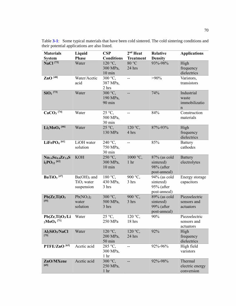
70
Table 3-1: Some typical materials that have been cold sintered. The cold sintering conditions and
their potential applications are also listed.
Materials
System
Liquid
Phase
CSP
Conditions
2nd Heat
Treatment
Relative
Density
Applications
NaCl [72] Water 120 °C,
300 MPa,
10 min
80 °C
24 hrs
93%-98% High
frequency
dielectrics
ZnO [48] Water/Acetic
acid
300 °C,
387 MPa,
2 hrs
-- >90% Varistors,
transistors
SiO2 [73] Water 300 °C,
190 MPa,
90 min
-- 74% Industrial
waste
immobilizatio
n
CaCO3 [74] Water 25 °C,
500 MPa,
30 min
-- 84% Construction
materials
Li2MoO4 [46] Water 25 °C,
130 MPa
120 °C,
4 hrs
87%-93% High
frequency
dielectrics
LiFePO4 [61] LiOH water
solution
240 °C,
750 MPa,
30 min
-- 85% Battery
cathodes
Na3.4Sc0.4Zr1.6S
i2PO12 [62]
KOH 250 °C,
300 MPa,
10 min
1000 °C,
1 hr
87% (as cold
sintered)
98% (after
post-anneal)
Battery
electrolytes
BaTiO3 [47] Ba(OH)2 and
TiO2 water
suspension
180 °C,
430 MPa,
3 hrs
900 °C,
3 hrs
94% (as cold
sintered)
95% (after
post-anneal)
Energy storage
capacitors
Pb(Zr,Ti)O3 [55]
Pb(NO3)2
water
solution
300 °C,
500 MPa,
3 hrs
900 °C,
3 hrs
89% (as cold
sintered)
99% (after
post-anneal)
Piezoelectric
sensors and
actuators
Pb(Zr,Ti)O3/Li
2MoO4 [71]
Water 25 °C,
250 MPa
120 °C,
18 hrs
90% Piezoelectric
sensors and
actuators
Al2SiO5/NaCl [75]
Water 120 °C,
200 MPa,
50 min
120 °C,
24 hrs
92% High
frequency
dielectrics
PTFE/ZnO [63] Acetic acid 285 °C,
300 MPa,
1 hr
-- 92%-96% High field
varistors
ZnO/MXene [65]
Acetic acid 300 °C,
250 MPa,
1 hr
-- 92%-98% Thermal
electric energy
conversion
71
A few general trends can be concluded from the table:
Transient liquid phase: The liquid phases used in CSP are often water-based solutions.
These solutions may cause either congruent dissolution (Li2MoO4 [46], KH2PO4 [47], NaNO2 [47],
ZnO [48], ZrO2 [76], etc.) or incongruent dissolution (BaTiO3 [47,77,78]) of the materials. Congruent
dissolution favors rapid densification via cold sintering, but is not always available in solids with
complex chemistries. For example, in the case of BaTiO3, the use of water as a liquid phase
promotes leaching of Ba2+ with subsequent formation of BaCO3 and passivation of the powder
surfaces with an unreactive hydrated titanium-rich surface layer that prevents densification [79].
Thus, to avoid incongruent dissolution of BaTiO3, a water based suspension of Ba(OH)2 and TiO2
can be utilized during cold sintering [77,78].
Temperature: The operation temperatures of CSP are below 300 °C. Generally, oxides
and complex compounds that are more difficult to dissolve are cold sintered at higher
temperatures. CSP is advantageous because of its operating temperatures; it is environmentally
friendly due to low energy consumption. New composites with ceramic inclusions beyond
percolation points can be fabricated by CSP without decomposition of polymer phases. [63,65]
Moreover, as sintering temperatures decrease, the energy for grain growth drops significantly,
enabling controllable microstructure engineering.
Pressure: Compared with uniaxial pressure by itself, the pressures applied during CSP are
much higher. This is likely to be part of what enables the ultra-low working temperatures; even
though dissolution of the ceramics can increase the diffusivities by 4-5 orders of magnitudes, the
grain growth during CSP is still not comparable with the conventional processes carried out at
higher temperatures. A study by Funahashi et al. [48] confirmed that CSP produces similarly dense
samples at lower temperature but with more limited grain growth than conventional methods. [80]
72
Density and secondary heat treatment: The relative densities of cold sintered materials are
mostly over 80% due to plastic deformation of powders during pressing. Sometimes the as-cold-
sintered samples need to be post-annealed at a higher temperature to eliminate secondary phases
and complete the sintering process. This procedure can be important for perovskites that are
difficult to dissolve congruently. In BaTiO3-based systems cold sintered in air using water as the
transient liquid phase, for example, CO2 stabilizes an amorphous phase that fills the pores
between the crystalline particles. This kinetically limits the sintering process until the carbonate is
decomposed at a temperature of ~ 830 °C. Therefore a post-annealing stage is required to further
densify and equilibrate the grain structures. A post-annealing at 900 °C produced high quality
BaTiO3 at a net reduction in temperature of 300-500 °C, relative to conventional methods [47]. The
result is well-densified ceramics with high dielectric performance.
Overall, CSP is still a technique under development. It remains promising despite
potential disadvantages such as secondary phase residue, incongruent dissolution of cations, and
restricted sample sizes/shapes due to pressure limits.
3.3 Experimental procedures
In this work, a Pb(NO3)2 solution was used as a transient liquid sintering aid to densify
PZT powder. This solution was selected for 4 reasons: its high solubility in water, its low
reactivity with CO2 (limiting carbonate secondary phases), its compensation for lead loss during
post annealing, and its ability to act as a liquid phase sintering aid during post annealing. A 0.5
mol/L Pb(NO3)2 solution was made by dissolving 5.02 g Pb(NO3)2 (Sigma-Aldrich Corp., St.
Louis, USA) into 30 mL deionized water.
A bimodal PZT powder was utilized for cold sintering PZT, as this leads to a higher
driving force for sintering and also can aid in the packing density. The coarse PZT powder is a
73
commercial PZT-5A powder (PKI-509, Piezo Kinetics, Inc., Bellefonte, PA). To reduce the
average particle size of ~ 3 μm, the powder was attrition milled (Szegvari Attritor System Type B
Model 01-HD, Union Process, Inc., Akron, OH) to an average diameter to ~ 400 nm. For the
attrition milling, 25 vol% PZT powder was suspended in deionized water with 3 vol% Darvan A-
21 dispersant (Vanderbilt Minerals, LLC, Norwalk, CT). The pH of the suspension was adjusted
to ~ 10 with NH4OH. The mixture was milled for 12 hours, dried at 200 °C, and heat treated at
500°C for 5 hours to remove any residual carbon.
The finer powder (undoped PZT 52/48) was made through a 2-methoxyethanol (2-MOE)
based sol-gel method as described elsewhere [81,82]. Lead acetate trihydrate (Sigma-Aldrich) was
added to 2-MOE in a rotary evaporator flask under Ar flow, dissolved at 120 °C and distilled
until a semi-dry powder precipitated. Zirconium n-propoxide (Sigma-Aldrich) and titanium iso-
propoxide (Sigma-Aldrich) were mixed in 2-MOE at room temperature, and then were added to
the lead acetate. The mixture was refluxed for 3 hours and distilled. Acetylacetone (22.5 vol%,
Sigma-Aldrich) and 2-MOE (Sigma-Aldrich) were added to make a 0.4 M solution. The solution
was dried by stirring in air on a hot plate at 120 °C until a gel formed. The gel was crushed in an
agate mortar and pestle and calcined at 600 °C for 42 hours to remove the residual carbon from
the precursors. The average diameter of the finer powder is ~ 100 nm.
To cold sinter PZT, 0.7 g of PZT bimodal powder (1:1 mixture of 400 nm and 100 nm
powders in terms of weight) was mixed with 0.5 ml lead nitrate solution and ground in a mortar
and pestle. The mixture was then loaded into a cylindrical die (Wartburg Tool & Die, Inc.,
Wartburg, TN) and pressed at 500 MPa uniaxial pressure (MP40 pellet press, Across
International, LLC, Livingston, NJ). The die was held at room temperature for 30 min, heated to
300 °C for 150 min and cooled down to < 80 °C in 30 min. The PZT pellets after cold sintering
had a diameter of 0.5 inch (12.77 mm) and thicknesses ~ 0.8-1.0 mm. Some of the cold sintered
74
PZT pellets underwent a post-annealing step at 700 °C for 3 h, 700 °C for 24 h, or 900 °C for 3 h.
The heating rate was 5 °C/min for all samples during the post-annealing process.
To compare with the cold sintering process, in a conventional method, 0.7 g bimodal PZT
powder was uniaxially pressed to a pellet under the same condition as CSP samples but without
the addition of Pb(NO3)2 solution. The conventionally pressed pellet was also annealed 900 °C
for 3 h, which is the same as the CSP sample.
For grain size measurement, the PZT samples were polished using 15 µm, 9 µm, 6 µm, 3
µm and 1 µm diamond polish, successively. Each step lasted for 2 min at a rotation speed of 240
rpm. The average grain size of the PZT samples was calculated by the line intercept method using
the equation shown below [83]:
𝐴𝑣𝑒𝑟𝑎𝑔𝑒 𝑔𝑟𝑎𝑖𝑛 𝑠𝑖𝑧𝑒 = 1.5 ×𝑡𝑜𝑡𝑎𝑙 𝑙𝑖𝑛𝑒 𝑙𝑒𝑛𝑔𝑡ℎ
𝑛𝑢𝑚𝑏𝑒𝑟 𝑜𝑓 𝑔𝑟𝑎𝑖𝑛 𝑏𝑜𝑢𝑛𝑑𝑎𝑟𝑖𝑒𝑠 (Eq. 3-5)
The crystal structure and phase purity of the PZT samples were identified by X-ray
diffraction (XRD, Empyrean, PANalytical Corp., Almelo, Netherlands) with Cu Kα radiation.
Scans were taken from 2θ = 10° to 72° with a step size of 0.026° 2θ and a scan rate of 0.067°/sec.
A scanning electron microscope (SEM, Merlin, Carl Zeiss, Inc., Jena, Germany) and a
transmission electron microscope (TEM, FEI Talos, Eindhoven, Netherlands) with an Energy
dispersive spectroscopy (EDS) detector were utilized to observe the microstructural development
of the ceramics. After cutting, polishing, and focused ion beam milling the samples to electron
transparency, they were mounted on copper grids.
The piezoelectric coefficients were measured by a direct method with a d33 PiezoMeter
system (PM 300, Piezotest Pte. Ltd., Singapore) after a poling process at 25 °C for an hour under
3 times the coercive field. The polarization-electric field hysteresis loops (P-E loops) were
characterized using a custom system with a Trek Model 30/20 high voltage amplifier system
(Trek, Inc., Lockport, NY) and LabVIEW software (National Instruments Corporation, Austin,
75
TX). The dielectric permittivity and loss tangent were measured using a Hewlett-Packard 4284A
LCR meter (Agilent Technologies, Inc., Palo Alto, CA) over a temperature range from 500 °C to
30 °C.
PZT powders with a bimodal size distribution (medium particle sizes of 50 nm and 600
nm) were used for the study of Pb(NO3)2 content, temperature, pressure and holding time. The
powder was produced by attrition milling (Szegvari Attritor System Type B Model 01-HD, Union
Process, Inc., Akron, OH) commercial PZT-5A powder (PKI-509, PiezoKinetics Inc., Bellefonte,
PA) for 12 hrs. The particle size analysis was double checked under a laser diffractometer
(Mastersize 3000, Malvern Analytical Ltd., Malvern, UK) and a scanning electron microscope
(Verios G4, FEI, Eindhoven, Netherlands).
The study on cold sintering temperature and pressure strained the capabilities of
conventional hydraulic presses as the heat from the die transferred to the hydraulic cylinder,
raised the oil temperature, and caused pressure fluctuations. An advanced hydraulic press with a
pressure stabilizing regulator, designed by Richard Floyd et al. [84], increased the repeatability of
CSP. This pressure regulator uses a spring-loaded nozzle to constrain oil flow and stabilize
pressure, allowing independent control of temperature and pressure. Following the designs of
Floyd, a new press was constructed. This press was utilized for research on cold sintering
temperature, pressure and time.
To make PZT pellets, 0.7 g (per pellet) raw powder was mixed and ground with different
volume fractions of Pb(NO3)2 powder (Sigma-Aldrich Corp., St. Louis, MO). 0.5 mL deionized
water was added to the mixture to dissolve the lead nitrate. The mixture was then ground in a
mortar and pestle until the water was mostly vaporized, removing the soft agglomerates in PZT.
After grinding, the mixture was loaded into a cylindrical die (Wartburg Tool & Die, Wartburg,
TN) and pressed at 25-300 °C, under 50-1000 MPa for 15-180 min. The pellets cold sintered at
76
<100 °C were dried in open air for over 24 hrs to remove residual water that might affect the
measured sintered density. The densities of the pellets were measured by the geometrical method.
3.4 Results and discussion
3.4.1 Cold sintering and electrical characterization of lead zirconate titanate piezoelectric
ceramics
Table 3-2 shows the geometric densities of PZT pellets with 15 vol% Pb(NO3)2 cold
sintered at 300 °C, 500 MPa for 3 hrs, and heat treated at different temperatures. Using a
theoretical density of 7.8 g/cm3, the green compact sample (pressed without the Pb(NO3)2
sintering aid) yields a relative density of 59%. Cold sintering at 300 °C increases the relative
density to 89%; after post-annealing at 900 °C the relative density increases to 99%.
Figure 3-7 shows the XRD patterns after cold sintering and post-annealing according to
the conditions mentioned in the above table. Crystalline Pb(NO3)2 and PbO are present after the
cold-sintering step because Pb(NO3)2 decomposes slowly from 250 °C. In contrast, after the post-
annealing step at higher temperatures the samples are XRD phase pure, as Pb(NO3)2 fully
Table 3-2: The densities and d33 of cold sintered (300 °C, 500 MPa, 3 hrs) PZT with different post-
annealing temperatures. The d33 values are the average of 3 measurements of the same sample for
each condition.
PZT samples Geometric
density
(g/cm3)
Relative
density
(%)
Dielectric
constant (100
kHz, 25 °C)
Loss
(%)
d33
(pC/N)
Green compact 300 °C
pressed
4.6 59 -- -- --
CSP 300 °C as sintered 6.9 89 207 2.0 4
CSP 700 °C 3 h post-
annealed
7.1 91 917 2.7 80
CSP 900 °C 3 h post-
annealed
7.7 99 1324 4.0 197
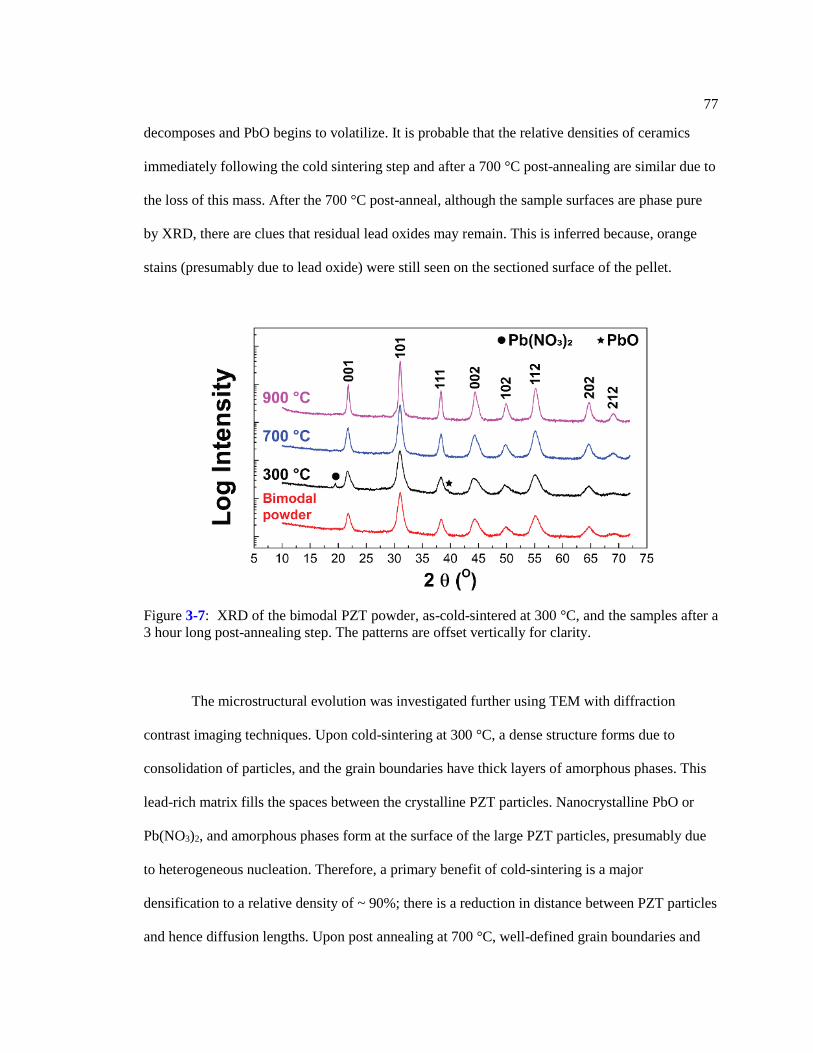
77
decomposes and PbO begins to volatilize. It is probable that the relative densities of ceramics
immediately following the cold sintering step and after a 700 °C post-annealing are similar due to
the loss of this mass. After the 700 °C post-anneal, although the sample surfaces are phase pure
by XRD, there are clues that residual lead oxides may remain. This is inferred because, orange
stains (presumably due to lead oxide) were still seen on the sectioned surface of the pellet.
The microstructural evolution was investigated further using TEM with diffraction
contrast imaging techniques. Upon cold-sintering at 300 °C, a dense structure forms due to
consolidation of particles, and the grain boundaries have thick layers of amorphous phases. This
lead-rich matrix fills the spaces between the crystalline PZT particles. Nanocrystalline PbO or
Pb(NO3)2, and amorphous phases form at the surface of the large PZT particles, presumably due
to heterogeneous nucleation. Therefore, a primary benefit of cold-sintering is a major
densification to a relative density of ~ 90%; there is a reduction in distance between PZT particles
and hence diffusion lengths. Upon post annealing at 700 °C, well-defined grain boundaries and
Figure 3-7: XRD of the bimodal PZT powder, as-cold-sintered at 300 °C, and the samples after a
3 hour long post-annealing step. The patterns are offset vertically for clarity.
78
equilibrated triple points started to form, with dihedral angles ~ 120o. When the temperature
increases to 900 °C, melting of PbO increases mass transport, bringing the densification to
completion. Within the grains, complex high-density domain configurations are formed as shown
in Figure 3-8 (f), (j) and (k). As for compositions, the EDS results presented in Figure B-1, B-2,
and B-3 indicate low carbon concentrations in cold sintered PZT although some zirconia
impurities, possibly from the commercial powder, were observed. This is shown in Figure B-1
(c).
Piezoelectric coefficients (d33) of the cold sintered PZT are listed in Table 3-2 as well.
The 900 °C annealed PZT has the highest d33 ~ 200 pC/N. This value is lower than commercial
PZT-5A (350-550 pC/N) probably because the addition of 50 wt% undoped PZT and the
nanograin size [12]. It nonetheless demonstrates that it is possible to cold sinter PZT while
retaining the functional properties, although at this point a post-annealing step is required to
remove the grain boundary phases, and obtain a better density. The 700 °C annealed sample has a
modest d33 most likely due to the presence of porosity, defects and residual lead oxides. For the
300 °C cold sintered sample, almost no piezoelectric behavior can be detected.
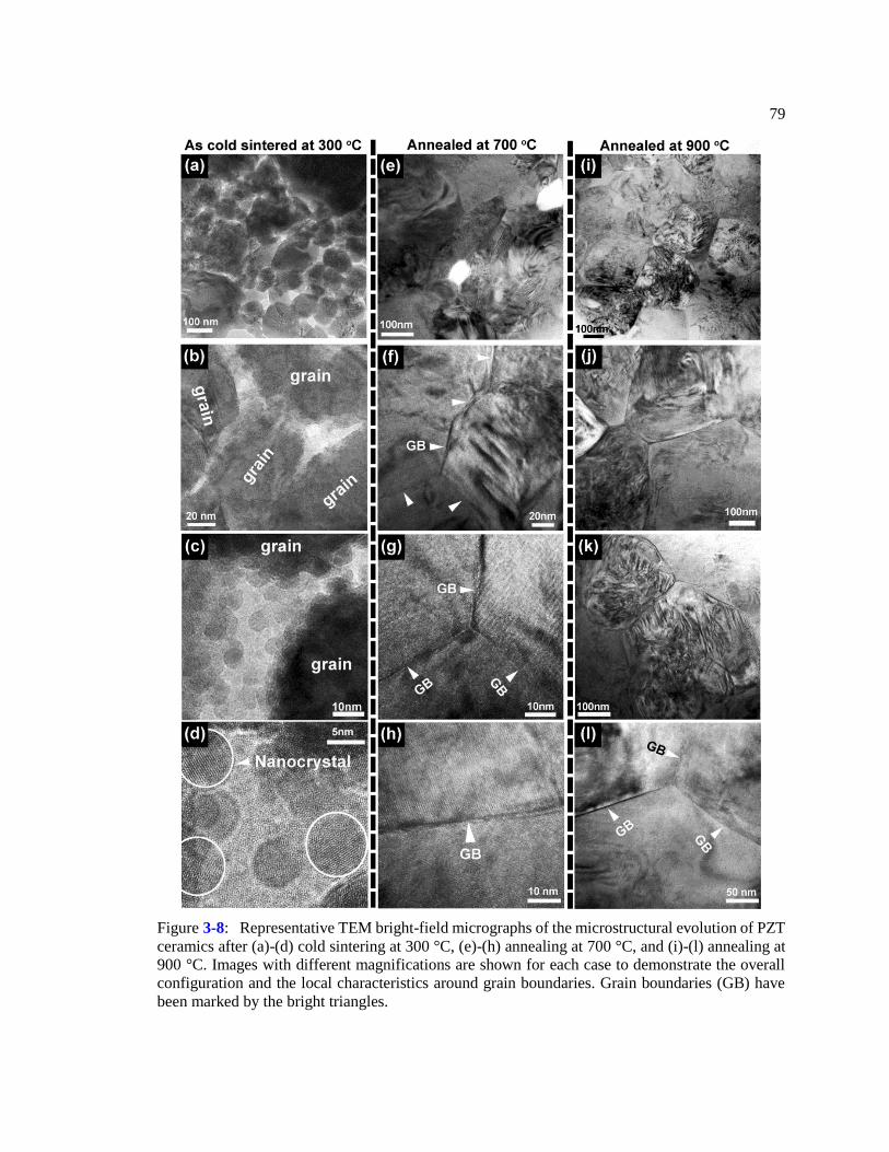
79
Figure 3-8: Representative TEM bright-field micrographs of the microstructural evolution of PZT
ceramics after (a)-(d) cold sintering at 300 °C, (e)-(h) annealing at 700 °C, and (i)-(l) annealing at
900 °C. Images with different magnifications are shown for each case to demonstrate the overall
configuration and the local characteristics around grain boundaries. Grain boundaries (GB) have
been marked by the bright triangles.
80
In Figure 3-9, the P-E loops and the permittivity-loss vs temperature curves of the PZT
samples processed at different conditions are compared. It is clear that the CSP PZT post-
annealed at 900 °C for 3 hrs has well saturated P-E loops with a higher remanent polarization and
lower coercive field than the PZT pressed without cold sintering with Pb(NO3)2 (Figure 3-9 (a)).
Moreover, (Figure 3-9 (c)), the dielectric permittivity of the 900 °C annealed CSP PZT is
significantly higher than that of 900 °C annealed PZT without the cold sintering step (~ 1380 vs.
~ 650 at room temperature). This is most likely due to the pores in the conventionally processed
PZT (Figure B-4) as it only has a geometric density ~ 75% after 900 °C annealing. The slightly
higher dielectric loss in the CSP PZT annealed at 900 °C is likely to be a consequence of domain
wall motion (the lower loss tangent at elevated temperatures suggests that the space charge
contribution to the loss tangent is reduced in the cold sintered specimens).[79]
The TEM data also suggests the possibility for reducing the maximum process
temperature of bulk PZT based on the closed triple point junctions. It was hypothesized that post-
annealing at 700°C for longer times may further improve the densification and yield better
properties. Attempting to verify this hypothesis, a 24 hour post-annealing procedure was utilized.
The sample had a similar P-E hysteresis loop as the 3-hour annealed sample when measured to
maximum fields of 40 kV/cm (Figure 3-9 (a)). On increasing the maximum field to 60 kV/cm, the
polarization hysteresis loop began to saturate, and showed a remanent polarization of 10 µC/cm2
(Figure 3-9 (b)). Furthermore, the longer anneal at 700°C produced a higher relative density (~
93%) and dielectric permittivity, as indicated by Figure 3-9 (c). In addition, the long-time
annealed PZT had a lower dielectric loss when the sample was heated to > 350 °C, suggesting the
reduction of excess PbO on increased annealing time.
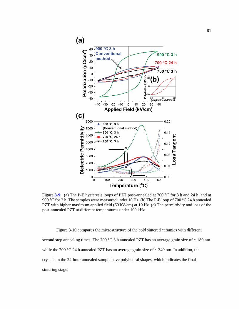
81
Figure 3-10 compares the microstructure of the cold sintered ceramics with different
second step annealing times. The 700 °C 3 h annealed PZT has an average grain size of ~ 180 nm
while the 700 °C 24 h annealed PZT has an average grain size of ~ 340 nm. In addition, the
crystals in the 24-hour annealed sample have polyhedral shapes, which indicates the final
sintering stage.
Figure 3-9: (a) The P-E hysteresis loops of PZT post-annealed at 700 °C for 3 h and 24 h, and at
900 °C for 3 h. The samples were measured under 10 Hz. (b) The P-E loop of 700 °C 24 h annealed
PZT with higher maximum applied field (60 kV/cm) at 10 Hz. (c) The permittivity and loss of the
post-annealed PZT at different temperatures under 100 kHz.
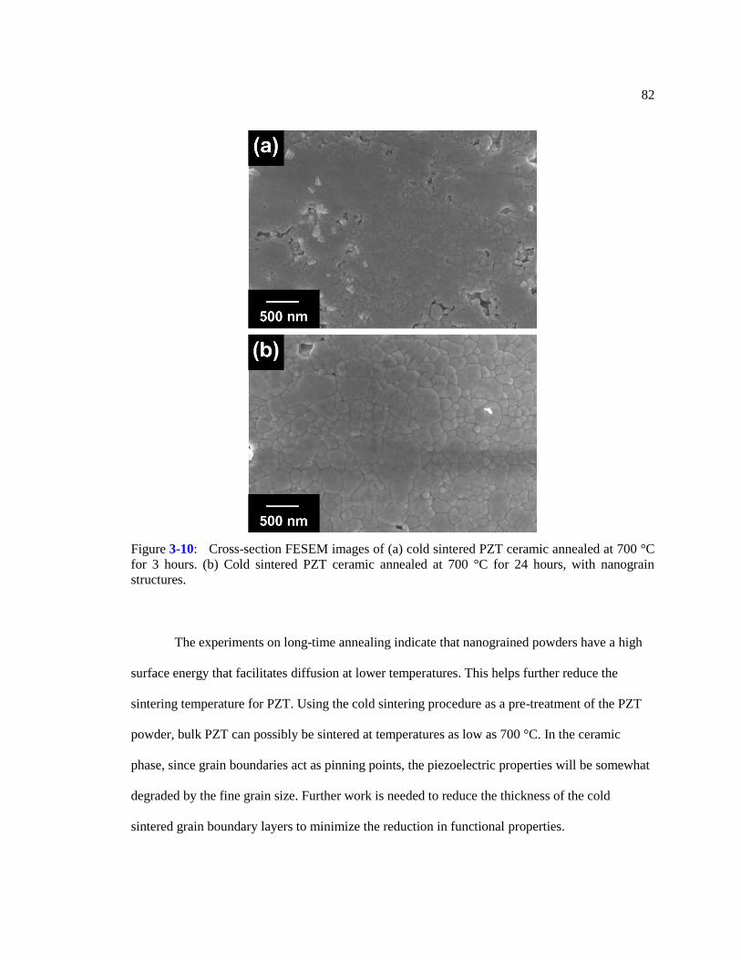
82
The experiments on long-time annealing indicate that nanograined powders have a high
surface energy that facilitates diffusion at lower temperatures. This helps further reduce the
sintering temperature for PZT. Using the cold sintering procedure as a pre-treatment of the PZT
powder, bulk PZT can possibly be sintered at temperatures as low as 700 °C. In the ceramic
phase, since grain boundaries act as pinning points, the piezoelectric properties will be somewhat
degraded by the fine grain size. Further work is needed to reduce the thickness of the cold
sintered grain boundary layers to minimize the reduction in functional properties.
Figure 3-10: Cross-section FESEM images of (a) cold sintered PZT ceramic annealed at 700 °C
for 3 hours. (b) Cold sintered PZT ceramic annealed at 700 °C for 24 hours, with nanograin
structures.
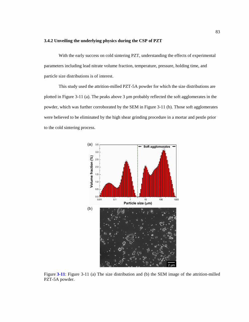
83
3.4.2 Unveiling the underlying physics during the CSP of PZT
With the early success on cold sintering PZT, understanding the effects of experimental
parameters including lead nitrate volume fraction, temperature, pressure, holding time, and
particle size distributions is of interest.
This study used the attrition-milled PZT-5A powder for which the size distributions are
plotted in Figure 3-11 (a). The peaks above 3 µm probably reflected the soft agglomerates in the
powder, which was further corroborated by the SEM in Figure 3-11 (b). Those soft agglomerates
were believed to be eliminated by the high shear grinding procedure in a mortar and pestle prior
to the cold sintering process.
Figure 3-11: Figure 3-11 (a) The size distribution and (b) the SEM image of the attrition-milled
PZT-5A powder.
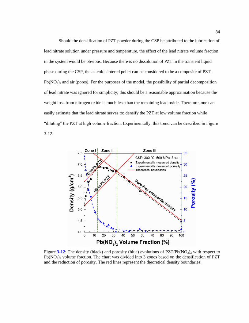
84
Should the densification of PZT powder during the CSP be attributed to the lubrication of
lead nitrate solution under pressure and temperature, the effect of the lead nitrate volume fraction
in the system would be obvious. Because there is no dissolution of PZT in the transient liquid
phase during the CSP, the as-cold sintered pellet can be considered to be a composite of PZT,
Pb(NO3)2 and air (pores). For the purposes of the model, the possibility of partial decomposition
of lead nitrate was ignored for simplicity; this should be a reasonable approximation because the
weight loss from nitrogen oxide is much less than the remaining lead oxide. Therefore, one can
easily estimate that the lead nitrate serves to: densify the PZT at low volume fraction while
“diluting” the PZT at high volume fraction. Experimentally, this trend can be described in Figure
3-12.
Figure 3-12: The density (black) and porosity (blue) evolutions of PZT/Pb(NO3)2 with respect to
Pb(NO3)2 volume fraction. The chart was divided into 3 zones based on the densification of PZT
and the reduction of porosity. The red lines represent the theoretical density boundaries.
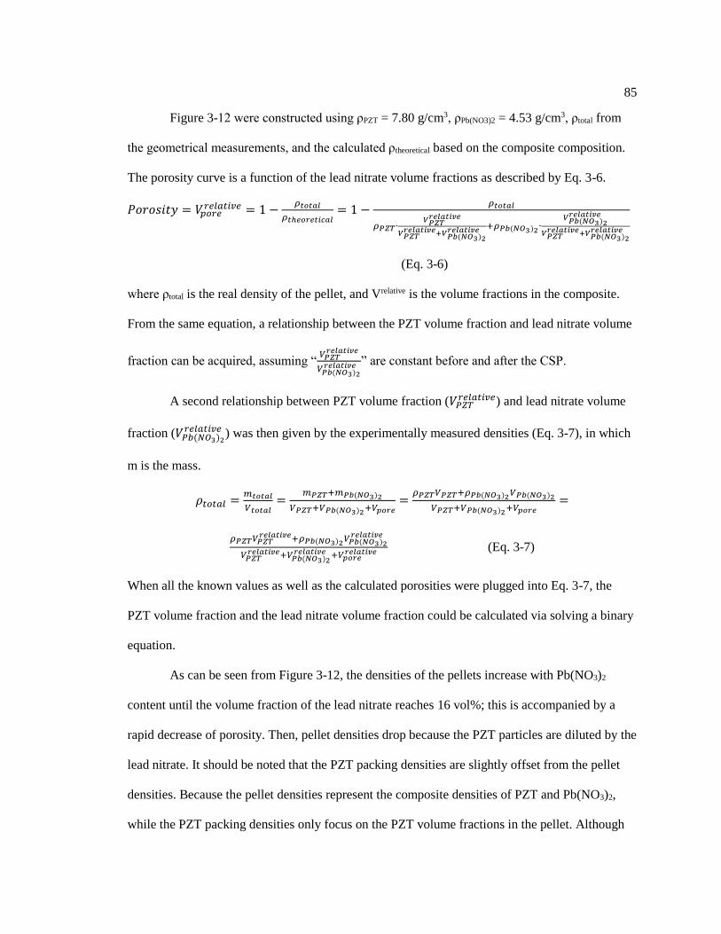
85
Figure 3-12 were constructed using ρPZT = 7.80 g/cm3, ρPb(NO3)2 = 4.53 g/cm3, ρtotal from
the geometrical measurements, and the calculated ρtheoretical based on the composite composition.
The porosity curve is a function of the lead nitrate volume fractions as described by Eq. 3-6.
𝑃𝑜𝑟𝑜𝑠𝑖𝑡𝑦 = 𝑉𝑝𝑜𝑟𝑒𝑟𝑒𝑙𝑎𝑡𝑖𝑣𝑒 = 1 −
𝜌𝑡𝑜𝑡𝑎𝑙
𝜌𝑡ℎ𝑒𝑜𝑟𝑒𝑡𝑖𝑐𝑎𝑙= 1 −
𝜌𝑡𝑜𝑡𝑎𝑙
𝜌𝑃𝑍𝑇∙𝑉𝑃𝑍𝑇𝑟𝑒𝑙𝑎𝑡𝑖𝑣𝑒
𝑉𝑃𝑍𝑇𝑟𝑒𝑙𝑎𝑡𝑖𝑣𝑒+𝑉𝑃𝑏(𝑁𝑂3)2
𝑟𝑒𝑙𝑎𝑡𝑖𝑣𝑒 +𝜌𝑃𝑏(𝑁𝑂3)2 ∙𝑉𝑃𝑏(𝑁𝑂3)2𝑟𝑒𝑙𝑎𝑡𝑖𝑣𝑒
𝑉𝑃𝑍𝑇𝑟𝑒𝑙𝑎𝑡𝑖𝑣𝑒+𝑉𝑃𝑏(𝑁𝑂3)2
𝑟𝑒𝑙𝑎𝑡𝑖𝑣𝑒
(Eq. 3-6)
where ρtotal is the real density of the pellet, and Vrelative is the volume fractions in the composite.
From the same equation, a relationship between the PZT volume fraction and lead nitrate volume
fraction can be acquired, assuming “𝑉𝑃𝑍𝑇
𝑟𝑒𝑙𝑎𝑡𝑖𝑣𝑒
𝑉𝑃𝑏(𝑁𝑂3)2𝑟𝑒𝑙𝑎𝑡𝑖𝑣𝑒 ” are constant before and after the CSP.
A second relationship between PZT volume fraction (𝑉𝑃𝑍𝑇𝑟𝑒𝑙𝑎𝑡𝑖𝑣𝑒) and lead nitrate volume
fraction (𝑉𝑃𝑏(𝑁𝑂3)2𝑟𝑒𝑙𝑎𝑡𝑖𝑣𝑒 ) was then given by the experimentally measured densities (Eq. 3-7), in which
m is the mass.
𝜌𝑡𝑜𝑡𝑎𝑙 =𝑚𝑡𝑜𝑡𝑎𝑙
𝑉𝑡𝑜𝑡𝑎𝑙=
𝑚𝑃𝑍𝑇+𝑚𝑃𝑏(𝑁𝑂3)2
𝑉𝑃𝑍𝑇+𝑉𝑃𝑏(𝑁𝑂3)2+𝑉𝑝𝑜𝑟𝑒
=𝜌𝑃𝑍𝑇𝑉𝑃𝑍𝑇+𝜌𝑃𝑏(𝑁𝑂3)2𝑉𝑃𝑏(𝑁𝑂3)2
𝑉𝑃𝑍𝑇+𝑉𝑃𝑏(𝑁𝑂3)2+𝑉𝑝𝑜𝑟𝑒
=
𝜌𝑃𝑍𝑇𝑉𝑃𝑍𝑇𝑟𝑒𝑙𝑎𝑡𝑖𝑣𝑒+𝜌𝑃𝑏(𝑁𝑂3)2𝑉𝑃𝑏(𝑁𝑂3)2
𝑟𝑒𝑙𝑎𝑡𝑖𝑣𝑒
𝑉𝑃𝑍𝑇𝑟𝑒𝑙𝑎𝑡𝑖𝑣𝑒+𝑉𝑃𝑏(𝑁𝑂3)2
𝑟𝑒𝑙𝑎𝑡𝑖𝑣𝑒 +𝑉𝑝𝑜𝑟𝑒𝑟𝑒𝑙𝑎𝑡𝑖𝑣𝑒 (Eq. 3-7)
When all the known values as well as the calculated porosities were plugged into Eq. 3-7, the
PZT volume fraction and the lead nitrate volume fraction could be calculated via solving a binary
equation.
As can be seen from Figure 3-12, the densities of the pellets increase with Pb(NO3)2
content until the volume fraction of the lead nitrate reaches 16 vol%; this is accompanied by a
rapid decrease of porosity. Then, pellet densities drop because the PZT particles are diluted by the
lead nitrate. It should be noted that the PZT packing densities are slightly offset from the pellet
densities. Because the pellet densities represent the composite densities of PZT and Pb(NO3)2,
while the PZT packing densities only focus on the PZT volume fractions in the pellet. Although
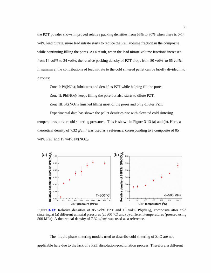
86
the PZT powder shows improved relative packing densities from 66% to 80% when there is 0-14
vol% lead nitrate, more lead nitrate starts to reduce the PZT volume fraction in the composite
while continuing filling the pores. As a result, when the lead nitrate volume fractions increases
from 14 vol% to 34 vol%, the relative packing density of PZT drops from 80 vol% to 66 vol%.
In summary, the contributions of lead nitrate to the cold sintered pellet can be briefly divided into
3 zones:
Zone I: Pb(NO3)2 lubricates and densifies PZT while helping fill the pores.
Zone II: Pb(NO3)2 keeps filling the pore but also starts to dilute PZT.
Zone III: Pb(NO3)2 finished filling most of the pores and only dilutes PZT.
Experimental data has shown the pellet densities rise with elevated cold sintering
temperatures and/or cold sintering pressures. This is shown in Figure 3-13 (a) and (b). Here, a
theoretical density of 7.32 g/cm3 was used as a reference, corresponding to a composite of 85
vol% PZT and 15 vol% Pb(NO3)2.
The liquid phase sintering models used to describe cold sintering of ZnO are not
applicable here due to the lack of a PZT dissolution-precipitation process. Therefore, a different
Figure 3-13: Relative densities of 85 vol% PZT and 15 vol% Pb(NO3)2 composite after cold
sintering at (a) different uniaxial pressures (at 300 °C) and (b) different temperatures (pressed using
500 MPa). A theoretical density of 7.32 g/cm3 was used as a reference.
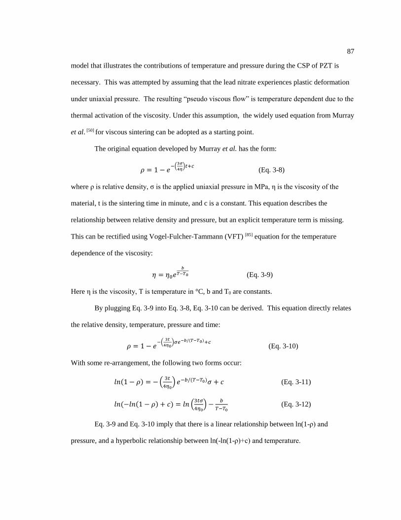
87
model that illustrates the contributions of temperature and pressure during the CSP of PZT is
necessary. This was attempted by assuming that the lead nitrate experiences plastic deformation
under uniaxial pressure. The resulting “pseudo viscous flow” is temperature dependent due to the
thermal activation of the viscosity. Under this assumption, the widely used equation from Murray
et al. [50] for viscous sintering can be adopted as a starting point.
The original equation developed by Murray et al. has the form:
𝜌 = 1 − 𝑒−(
3𝜎
4𝜂)𝑡+𝑐
(Eq. 3-8)
where ρ is relative density, σ is the applied uniaxial pressure in MPa, η is the viscosity of the
material, t is the sintering time in minute, and c is a constant. This equation describes the
relationship between relative density and pressure, but an explicit temperature term is missing.
This can be rectified using Vogel-Fulcher-Tammann (VFT) [85] equation for the temperature
dependence of the viscosity:
𝜂 = 𝜂0𝑒𝑏
𝑇−𝑇0 (Eq. 3-9)
Here η is the viscosity, T is temperature in °C, b and T0 are constants.
By plugging Eq. 3-9 into Eq. 3-8, Eq. 3-10 can be derived. This equation directly relates
the relative density, temperature, pressure and time:
𝜌 = 1 − 𝑒−(
3𝑡
4𝜂0)𝜎𝑒−𝑏/(𝑇−𝑇0)+𝑐
(Eq. 3-10)
With some re-arrangement, the following two forms occur:
𝑙𝑛(1 − 𝜌) = −(3𝑡
4𝜂0) 𝑒−𝑏/(𝑇−𝑇0)𝜎 + 𝑐 (Eq. 3-11)
𝑙𝑛(−𝑙𝑛(1 − 𝜌) + 𝑐) = 𝑙𝑛 (3𝑡𝜎
4𝜂0) −
𝑏
𝑇−𝑇0 (Eq. 3-12)
Eq. 3-9 and Eq. 3-10 imply that there is a linear relationship between ln(1-ρ) and
pressure, and a hyperbolic relationship between ln(-ln(1-ρ)+c) and temperature.
88
Fig. 3-14 (a) shows the experimental data plotted as for Equation 3-8. Fitting the 300 °C
data in Figure 3-14 (a) gives Eq. 3-13:
𝑙𝑛(1 − 𝜌)𝑇=300 °𝐶 = −0.00254 ± 0.000313𝜎 − 1.30 ± 0.138 (Eq. 3-13)
Using c = -1.30 in Eq. 3-12, Figure 3-14 (b) can be plotted and Eq. 3-12 can be
parameterized as Eq. 3-14:
𝑙𝑛(−𝑙𝑛(1 − 𝜌) + 𝑐) = −4.21 ± 1.79 −1790±1890
𝑇−696±274 (Eq. 3-14)
These fits give R2 of 0.94 for the density-pressure relationship and 0.98 for the density-
temperature relationship, suggesting the cold sintering of PZT can possibly be reasonably
described as a viscous-sintering-related process.
Meanwhile, the fitting in Eq. 3-14 indicates large standard deviations for b and T0. This is
mostly likely because the curve shape from the VFT model is insensitive to b and T0 changes in
this temperature range. Thus, an alternative fitting strategy is to apply the Arrhenius relationship
(Eq. 3-15), resulting in two linear relationships (Eq. 3-16 and Eq. 3-17):
Figure 3-14: The experimental data in Figure 3-13 is replotted in the forms of (a) Eq. 3-11 and (b)
Eq. 3-12/Eq. 3-17, respectively. Relative densities vs. uniaxial pressures acquired at room
temperature are shown by a blue curve in (a). The dashed lines in (a) represent the predictions from
the model with VFT and Reynold’s equations. (The slopes and intercepts of the predictions from
VFT and Reynold-based models are too close to differentiate the two dashed lines in the figure.)
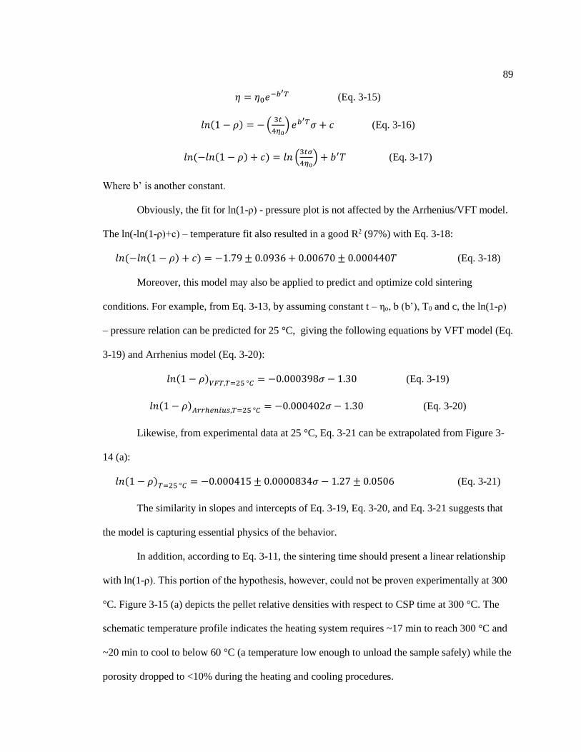
89
𝜂 = 𝜂0𝑒−𝑏′𝑇 (Eq. 3-15)
𝑙𝑛(1 − 𝜌) = −(3𝑡
4𝜂0) 𝑒𝑏′𝑇𝜎 + 𝑐 (Eq. 3-16)
𝑙𝑛(−𝑙𝑛(1 − 𝜌) + 𝑐) = 𝑙𝑛 (3𝑡𝜎
4𝜂0) + 𝑏′𝑇 (Eq. 3-17)
Where b’ is another constant.
Obviously, the fit for ln(1-ρ) - pressure plot is not affected by the Arrhenius/VFT model.
The ln(-ln(1-ρ)+c) – temperature fit also resulted in a good R2 (97%) with Eq. 3-18:
𝑙𝑛(−𝑙𝑛(1 − 𝜌) + 𝑐) = −1.79 ± 0.0936 + 0.00670 ± 0.000440𝑇 (Eq. 3-18)
Moreover, this model may also be applied to predict and optimize cold sintering
conditions. For example, from Eq. 3-13, by assuming constant t – ηo, b (b’), T0 and c, the ln(1-ρ)
– pressure relation can be predicted for 25 °C, giving the following equations by VFT model (Eq.
3-19) and Arrhenius model (Eq. 3-20):
𝑙𝑛(1 − 𝜌)𝑉𝐹𝑇,𝑇=25 °𝐶 = −0.000398𝜎 − 1.30 (Eq. 3-19)
𝑙𝑛(1 − 𝜌)𝐴𝑟𝑟ℎ𝑒𝑛𝑖𝑢𝑠,𝑇=25 °𝐶 = −0.000402𝜎 − 1.30 (Eq. 3-20)
Likewise, from experimental data at 25 °C, Eq. 3-21 can be extrapolated from Figure 3-
14 (a):
𝑙𝑛(1 − 𝜌)𝑇=25 °𝐶 = −0.000415 ± 0.0000834𝜎 − 1.27 ± 0.0506 (Eq. 3-21)
The similarity in slopes and intercepts of Eq. 3-19, Eq. 3-20, and Eq. 3-21 suggests that
the model is capturing essential physics of the behavior.
In addition, according to Eq. 3-11, the sintering time should present a linear relationship
with ln(1-ρ). This portion of the hypothesis, however, could not be proven experimentally at 300
°C. Figure 3-15 (a) depicts the pellet relative densities with respect to CSP time at 300 °C. The
schematic temperature profile indicates the heating system requires ~17 min to reach 300 °C and
~20 min to cool to below 60 °C (a temperature low enough to unload the sample safely) while the
porosity dropped to <10% during the heating and cooling procedures.
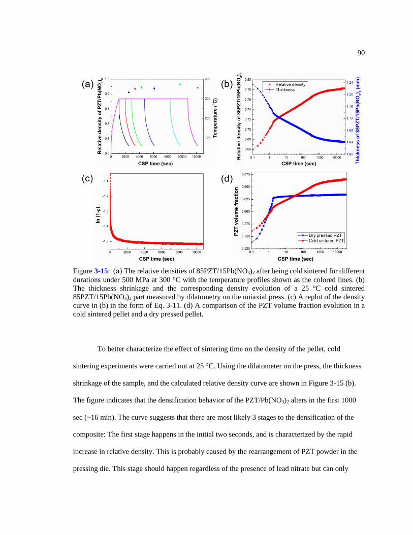
90
To better characterize the effect of sintering time on the density of the pellet, cold
sintering experiments were carried out at 25 °C. Using the dilatometer on the press, the thickness
shrinkage of the sample, and the calculated relative density curve are shown in Figure 3-15 (b).
The figure indicates that the densification behavior of the PZT/Pb(NO3)2 alters in the first 1000
sec (~16 min). The curve suggests that there are most likely 3 stages to the densification of the
composite: The first stage happens in the initial two seconds, and is characterized by the rapid
increase in relative density. This is probably caused by the rearrangement of PZT powder in the
pressing die. This stage should happen regardless of the presence of lead nitrate but can only
Figure 3-15: (a) The relative densities of 85PZT/15Pb(NO3)2 after being cold sintered for different
durations under 500 MPa at 300 °C with the temperature profiles shown as the colored lines. (b)
The thickness shrinkage and the corresponding density evolution of a 25 °C cold sintered
85PZT/15Pb(NO3)2 part measured by dilatometry on the uniaxial press. (c) A replot of the density
curve in (b) in the form of Eq. 3-11. (d) A comparison of the PZT volume fraction evolution in a
cold sintered pellet and a dry pressed pellet.
91
achieve limited densification. The second stage occurs from ~3 – ~1000 sec, during which the
densification of the composite slows down. It is speculated that this is related to a combination of
viscous sintering and water evaporation. Specifically, the lead nitrate starts to deform under
pressure and moisture, enabling the further optimization of PZT compaction; as the water escapes
from the die, the re-precipitation of lead nitrate causes a shrinkage in volume. After 16 min of
cold sintering at room temperature, the rearrangement of PZT becomes significantly retarded as
the packing is close to its geometrical limit.
The ln(1-ρ) vs time curve was obtained by replotting Figure 3-15 (b) in the form of Eq. 3-
11, and is shown in Figure 3-15 (c). It is obvious that the modified viscous sintering equation
failed to describe, at least for the first 16 min, that ln(1-ρ) is linearly related to the cold sintering
time at room temperature, presumably because the cold sintering process is complicated by the
initial particle rearrangements and the water volatilization process. In stage 3 of the CSP (after 16
min), the curve presents a more linear shape and the fitting R2 returns to 78%.
To test the hypothesis regarding stage 2, the dilatometry curves of a cold sintered sample
and a dry pressed sample are shown in Figure 3-15 (d). Notice that the y axis has been replaced
by PZT volume fraction to facilitate comparison between the two samples. It is clear that both
systems experience the rapid loose packing in the first 2 sec. However, while the dry pressed
sample displays almost no densification over the next couple of hours, the density of the cold
sintered sample continues to increase, which corroborates the previous hypothesis that the
moisturized lead nitrate can further optimize the packing of the particles. Interestingly, at the end
of the first stage, the PZT volume fraction of the dry pressed sample is a little higher than the cold
sintered sample. This is possibly because the addition of moisturized lead nitrate will hinder the
rapid particle rearrangement by thickening the spacing between PZT particles, but this effect can
be mitigated as the lead nitrate deforms in the following 16 min and eventually leads to a higher
density.
92
3.5 Conclusions
PZT ceramics were cold sintered to >80% relative densities at 300 °C using bimodal PZT
powder with moisturized Pb(NO3)2 as a sintering aid. The underlying mechanism of PZT
densification during cold sintering is improved PZT particle packing induced by the plastic
deformation of either moisturized lead nitrate or lead oxide. Therefore, a viscous sintering model
can be utilized to explain the effects of temperature, pressure and time on the final pellet
densities; the model showed good agreement with experimental results in terms of pressure and
temperature, while the particle rearrangement at the initial stage of CSP deviates the behavior of
densification with respect to time. Because there is no noticeable necking between PZT particles
during cold sintering with lead nitrate, a post-annealing procedure at 900 °C for 3 hours, which is
300-400 °C lower than conventional methods, is needed to develop good ferroelectric properties.
In addition, 700 °C annealing indicated promising densification for longer annealing times. The
post-annealing step promotes densification improvement and equilibration of a nanosized grain
structure; it produces ceramics with high relative permittivity, well-developed polarization
switching with high remanent polarizations, and strong piezoelectric coefficients.
References
[1] Kishi, H.; Mizuno, Y.; Chazono, H. Base-Metal Electrode-Multilayer Ceramic Capacitors:
Past, Present and Future Perspectives. Japanese J. Appl. Physics, Part 1 Reg. Pap. Short Notes
Rev. Pap. 2003, 42 (1), 1–5.
[2] Levinson, L. M.; Philipp, H. R. Zinc Oxide Varistors ― A Review. Am. Ceram. Soc. Bull.
1986, 65 (4), 639–647.
93
[3] Ohtaki, M. Recent Aspects of Oxide Thermoelectric Materials for Power Generation from
Mid-to-High Temperature Heat Source. J. Ceram. Soc. Japan 2011, 119 (1395), 770–775.
[4] Kok, S. L.; White, N. M.; Harris, N. R. Free-Standing Thick-Film Piezoelectric Multimorph
Cantilevers for Energy Harvesting. IEEE International Ultrasonics Symposium; IEEE, 2009,
1977–1980.
[5] Snaith, H. J. Present Status and Future Prospects of Perovskite Photovoltaics. Nat. Mater.
2018, 17 (5), 372–376.
[6] Padhi, A. K.; Nanjundaswamy, K. S.; Goodenough, J. B. Phospho-Olivines as Positive-
Electrode Materials for Rechargeable Lithium Batteries. J. Electrochem. Soc. 1997, 144 (4),
1188.
[7] Wang, Z.; Xue, Q.-T.; Chen, Y.-Q.; Shu, Y.; Tian, H.; Yang, Y.; Xie, D.; Luo, J.-W.; Ren, T.-
L. A Flexible Ultrasound Transducer Array with Micro-Machined Bulk PZT. Sensors 2015, 15
(2), 2538–2547.
[8] Miyahara, Y.; Deschler, M.; Fujii, T.; Watanabe, S.; Bleuler, H. Non-Contact Atomic Force
Microscope with a PZT Cantilever Used for Deflection Sensing, Direct Oscillation and Feedback
Actuation. Appl. Surf. Sci. 2002, 188 (3–4), 450–455.
[9] Yeo, H. G.; Ma, X.; Rahn, C.; Trolier-McKinstry, S. Efficient Piezoelectric Energy Harvesters
Utilizing (001) Textured Bimorph PZT Films on Flexible Metal Foils. Adv. Funct. Mater. 2016,
26 (32), 5940–5946.
[10] Cho, S. H.; Biggers, J. V. Characterization and Sintering of Lead Zirconate-Titanate
Powders. J. Am. Ceram. Soc. 1983, 66 (10), 743–746.
[11] Haertling, G. H. Grain Growth and Densification of Hot‐Pressed Lead Zirconate‐Lead
Titanate Ceramics Containing Bismuth. J. Am. Ceram. Soc. 1966, 49 (3), 113–118.
94
[12] Randall, C. A.; Kim, N.; Kucera, J.-P.; Cao, W.; Shrout, T. R. Intrinsic and Extrinsic Size
Effects in Fine-Grained Morphotropic-Phase-Boundary Lead Zirconate Titanate Ceramics. J. Am.
Ceram. Soc. 2005, 81 (3), 677–688.
[13] Atkin, R. B.; Fulrath, R. M. Point Defects and Sintering of Lead Zirconate-Titanate. J. Am.
Ceram. Soc. 1971, 54 (5), 265–270.
[14] Hayashi, T.; Inoue, T.; Nagashima, Y.; Tomizawa, J.; Akiyama, Y. Low-Temperature
Sintering of PZT with LiBiO2 as a Sintering Aid. Ferroelectrics 2001, 258 (1), 53–60.
[15] Hayashi, T.; Inoue, T.; Akiyama, Y. Low Temperature Sintering of PZT Powders Coated
with Pb5Ge3O11 by Sol–Gel Method. J. Eur. Ceram. Soc. 1999, 19 (6–7), 999–1002.
[16] Sharma, P. K.; Ounaies, Z.; Varadan, V. V; Varadan, V. K. Dielectric and Piezoelectric
Properties of Microwave Sintered PZT. Smart Mater. Struct. 2001, 10 (5), 878–883.
[17] Wu, Y. J.; Li, J.; Kimura, R.; Uekawa, N.; Kakegawa, K. Effects of Preparation Conditions
on the Structural and Optical Properties of Spark Plasma-Sintered PLZT (8/65/35) Ceramics. J.
Am. Ceram. Soc. 2005, 88 (12), 3327–3331.
[18] Bansal, N. P.; Boccaccini, A. R. Eds. Ceramics and Composites Processing Methods; John
Wiley & Sons, Inc.: Hoboken, NJ, USA, 2012.
[19] Bordia, R. K.; Kang, S. J. L.; Olevsky, E. A. Current Understanding and Future Research
Directions at the Onset of the next Century of Sintering Science and Technology. J. Am. Ceram.
Soc. 2017, 100 (6), 2314–2352.
[20] Rahaman, M. N. Ceramic Processing and Sintering, 2nd ed.; CRC Press: New York, NY,
2003.
[21] Houabes, M.; Bernik, S.; Talhi, C.; Bui, A. The Effect of Aluminium Oxide on the Residual
Voltage of ZnO Varistors. Ceram. Int. 2005, 31 (6), 783–789.
95
[22] Gibson, I. R.; Dransfield, G. P.; Irvine, J. T. S. Sinterability of Commercial 8 Mol% Yttria-
Stabilized Zirconia Powders and the Effect of Sintered Density on the Ionic Conductivity. J.
Mater. Sci. 1998, 33 (17), 4297–4305.
[23] Lu, W.; Quilitz, M.; Schmidt, H. Nanoscaled BaTiO3 Powders with a Large Surface Area
Synthesized by Precipitation from Aqueous Solutions: Preparation, Characterization and
Sintering. J. Eur. Ceram. Soc. 2007, 27 (10), 3149–3159.
[24] Coble, R. L. Sintering Crystalline Solids. I. Intermediate and Final State Diffusion Models. J.
Appl. Phys. 1961, 32 (5), 787–792.
[25] Rojac, T.; Bencan, A.; Malic, B.; Tutuncu, G.; Jones, J. L.; Daniels, J. E.; Damjanovic, D.
BiFeO3 Ceramics: Processing, Electrical, and Electromechanical Properties. J. Am. Ceram. Soc.
2014, 97 (7), 1993–2011.
[26] Gubernat, A.; Rutkowski, P.; Grabowski, G.; Zientara, D. Hot Pressing of Tungsten Carbide
with and without Sintering Additives. Int. J. Refract. Met. Hard Mater. 2014, 43, 193–199.
[27] Ekström, T.; Käll, P. O.; Nygren, M.; Olsson, P. O. Dense Single-Phase β-Sialon Ceramics
by Glass-Encapsulated Hot Isostatic Pressing. Journal of Materials Science. 1989, pp 1853–1861.
[28] Kwon, O. H.; Messing, G. L. A Theoretical Analysis of Solution-Precipitation Controlled
Densification during Liquid Phase Sintering. Acta Metall. Mater. 1991, 39 (9), 2059–2068.
[29] Carter, C. B.; Norton, M. G. Ceramic Materials: Science and Engineering, 2nd ed.; Springer
New York: New York, NY, 2013.
[30] Sutorik, A. C.; Gilde, G.; Cooper, C.; Wright, J.; Hilton, C. The Effect of Varied Amounts of
LiF Sintering Aid on the Transparency of Alumina Rich Spinel Ceramic with the Composition
MgO·1.5 Al2O3. J. Am. Ceram. Soc. 2012, 95 (6), 1807–1810.
[31] Suprapedi; Sardjono, P.; Muljadi; Rusnaeni, N.; Humaidi, S. Effect of Additive Na2O on
Sintering Temperature, Crystal Structure and Magnetic Properties of BaFe12O19 Magnet. J. Phys.
Conf. Ser. 2017, 817 (1), 012056.
96
[32] Xia, W. S.; Li, L. X.; Zhang, P.; Ning, P. F. Effects of CaF2 Addition on Sintering Behavior
and Microwave Dielectric Properties of ZnTa2O6 Ceramics. Mater. Lett. 2011, 65 (21–22), 3317–
3319.
[33] Hagiwara, M.; Fujihara, S. Effects of CuO Addition on Electrical Properties of 0.6BiFeO3-
0.4(Bi0.5K0.5)TiO3 Lead-Free Piezoelectric Ceramics. J. Am. Ceram. Soc. 2015, 98 (2), 469–475.
[34] Yuksel, B.; Ozkan, T. O. Grain Growth Kinetics for B2O3-Doped ZnO Ceramics. Mater. Sci.
2015, 33 (2), 220–229.
[35] Corker, D. L.; Whatmore, R. W.; Ringgaard, E.; Wolny, W. W. Liquid-Phase Sintering of
PZT Ceramics. J. Eur. Ceram. Soc. 2000, 20 (12), 2039–2045.
[36] Wu, J.; Chang, Y.; Yang, B.; Wang, X.; Zhang, S.; Sun, Y.; Qi, X.; Wang, J.; Cao, W.
Densification Behavior and Electrical Properties of CuO-Doped Pb(In1/2Nb1/2)O3-
Pb(Mg1/3Nb2/3)O3-PbTiO3 Ternary Ceramics. Ceram. Int. 2016, 42 (6), 7223–7229.
[37] Medesi, A.; Greiner, T.; Benkler, M.; Megnin, C.; Hanemann, T. Low Temperature Sintering
of PZT. J. Phys. Conf. Ser. 2014, 557, 012132.
[38] Kingon, A. I.; Clark, J. B. Sintering of PZT Ceramics: II, Effect of PbO Content on
Densification Kinetics. J. Am. Ceram. Soc. 1982, 66 (4), 256–260.
[39] Varshneya, A.; Mauro, J. Fundamentals of Inorganic Glasses, 3rd ed.; Academic Press:
London, UK, 2019.
[40] Agrawal, D. Microwave Sintering of Ceramics, Composites and Metallic Materials, and
Melting of Glasses. Trans. Indian Ceram. Soc. 2006, 65 (3), 129–144.
[41] Grasso, S.; Poetschke, J.; Richter, V.; Maizza, G.; Sakka, Y.; Reece, M. J. Low-Temperature
Spark Plasma Sintering of Pure Nano WC Powder. J. Am. Ceram. Soc. 2013, 96 (6), 1702–1705.
[42] Cheng, J.; Agrawal, D.; Roy, R.; Jayan, P. S. Continuous Microwave Sintering of Alumina
Abrasive Grits. J. Mater. Process. Technol. 2000, 108 (1), 26–29.
97
[43] Biesuz, M.; Sglavo, V. M. Flash Sintering of Ceramics. J. Eur. Ceram. Soc. 2019, 39 (2–3),
115–143.
[44] Vaidhyanathan, B.; Singh, A. P.; Agrawal, D. K.; Shrout, T. R.; Roy, R.; Ganguly, S.
Microwave Effects in Lead Zirconium Titanate Synthesis: Enhanced Kinetics and Changed
Mechanisms. J. Am. Ceram. Soc. 2004, 84 (6), 1197–1202.
[45] Dargatz, B.; Gonzalez-Julian, J.; Guillon, O. Effect of Electric Field and Atmosphere on the
Processing of Nanocrystalline ZnO. Proc. of SPIE. 2014, 89871H, 1-8.
[46] Kahari, H.; Teirikangas, M.; Juuti, J.; Jantunen, H. Dielectric Properties of Lithium
Molybdate Ceramic Fabricated at Room Temperature. J. Am. Ceram. Soc. 2014, 97 (11), 3378–
3379.
[47] Guo, H.; Baker, A.; Guo, J.; Randall, C. A. Cold Sintering Process: A Novel Technique for
Low-Temperature Ceramic Processing of Ferroelectrics. J. Am. Ceram. Soc. 2016, 99 (11),
3489–3507.
[48] Funahashi, S.; Guo, J.; Guo, H.; Wang, K.; Baker, A. L.; Shiratsuyu, K.; Randall, C. A.
Demonstration of the Cold Sintering Process Study for the Densification and Grain Growth of
ZnO Ceramics. J. Am. Ceram. Soc. 2017, 100 (2), 546–553.
[49] Guo, J.; Guo, H.; Baker, A. L.; Lanagan, M. T.; Kupp, E. R.; Messing, G. L.; Randall, C. A.
Cold Sintering: A Paradigm Shift for Processing and Integration of Ceramics. Angew. Chemie -
Int. Ed. 2016, 55 (38), 11457–11461.
[50] Murray, P.; Rodgers, E. P.; Williams, A. E. Practical and Theoretical Aspects of Hot
Pressing of Refractory Oxides. Trans. Br. Ceram. Soc. 1954, 53 (8), 474–510.
[51] Gutmanas, E. Y.; Lawley, A. Cold Sinteirng - A New Powder Consolidation Process. Prog.
Powder Metall. 1983, 39, 1–15.
[52] Roy, D. M.; Gouda, G. R.; Bobrowsky, A. Very High Strength Cement Pastes Prepared by
Hot Pressing and Other High Pressure Techniques. Cem. Concr. Res. 1972, 2 (3), 349–366.
98
[53] Yamasaki, N.; Yanagisawa, K.; Nishioka, M.; Kanahara, S. A Hydrothermal Hot-Pressing
Method: Apparatus and Application. J. Mater. Sci. Lett. 1986, 5, 355–356.
[54] Guo, H.; Bayer, T. J. M.; Guo, J.; Baker, A.; Randall, C. A. Cold Sintering Process for 8
Mol%Y2O3-Stabilized ZrO2 Ceramics. J. Eur. Ceram. Soc. 2017, 37 (5), 2303–2308.
[55] Wang, D.; Guo, H.; Morandi, C. S.; Randall, C. A.; Trolier-McKinstry, S. Cold Sintering
and Electrical Characterization of Lead Zirconate Titanate Piezoelectric Ceramics. APL Mater.
2018, 6 (1), 016101.
[56] Liu, J. A.; Li, C. H.; Shan, J. J.; Wu, J. M.; Gui, R. F.; Shi, Y. S. Preparation of High-
Density InGaZnO4 Target by the Assistance of Cold Sintering. Mater. Sci. Semicond. Process.
2018, 84, 17–23.
[57] Huang, H. Q.; Tang, J.; Liu, J. Preparation of Na0.5Bi0.5TiO3 Ceramics by Hydrothermal-
Assisted Cold Sintering. Ceram. Int. 2019, 45 (6), 6753–6758.
[58] Ma, J.; Li, H.; Wang, H.; Lin, C.; Wu, X.; Lin, T.; Zheng, X.; Yu, X. Composition,
Microstructure and Electrical Properties of K0.5Na0.5NbO3 Ceramics Fabricated by Cold Sintering
Assisted Sintering. J. Eur. Ceram. Soc. 2019, 39 (4), 986–993.
[59] Lee, W.; Lyon, C. K.; Seo, J. H.; Lopez-Hallman, R.; Leng, Y.; Wang, C. Y.; Hickner, M.
A.; Randall, C. A.; Gomez, E. D. Ceramic–Salt Composite Electrolytes from Cold Sintering.
Adv. Funct. Mater. 2019, 29 (20), 1–8.
[60] Hong, W. Bin; Li, L.; Cao, M.; Chen, X. M. Plastic Deformation and Effects of Water in
Room-Temperature Cold Sintering of NaCl Microwave Dielectric Ceramics. J. Am. Ceram. Soc.
2018, 101 (9), 4038–4043.
[61] Seo, J. H.; Guo, J.; Guo, H.; Verlinde, K.; Heidary, D. S. B.; Rajagopalan, R.; Randall, C. A.
Cold Sintering of a Li-Ion Cathode: LiFePO4-Composite with High Volumetric Capacity. Ceram.
Int. 2017, 43 (17), 15370–15374.
99
[62] Pereira da Silva, J. G.; Bram, M.; Laptev, A. M.; Gonzalez-Julian, J.; Ma, Q.; Tietz, F.;
Guillon, O. Sintering of a Sodium-Based NASICON Electrolyte: A Comparative Study between
Cold, Field Assisted and Conventional Sintering Methods. J. Eur. Ceram. Soc. 2019, 39 (8),
2697–2702.
[63] Zhao, X.; Guo, J.; Wang, K.; Herisson De Beauvoir, T.; Li, B.; Randall, C. A. Introducing a
ZnO–PTFE (Polymer) Nanocomposite Varistor via the Cold Sintering Process. Adv. Eng. Mater.
2018, 20 (7), 1–8.
[64] Zhao, Y.; Berbano, S. S.; Gao, L.; Wang, K.; Guo, J.; Tsuji, K.; Wang, J.; Randall, C. A.
Cold-Sintered V2O5-PEDOT:PSS Nanocomposites for Negative Temperature Coefficient
Materials. J. Eur. Ceram. Soc. 2019, 39 (4), 1257–1262.
[65] Guo, J.; Legum, B.; Anasori, B.; Wang, K.; Lelyukh, P.; Gogotsi, Y.; Randall, C. A. Cold
Sintered Ceramic Nanocomposites of 2D MXene and Zinc Oxide. Adv. Mater. 2018, 30 (32), 1–
6.
[66] Wang, D.; Zhou, D.; Zhang, S.; Vardaxoglou, Y.; Whittow, W. G.; Cadman, D.; Reaney, I.
M. Cold-Sintered Temperature Stable Na0.5Bi0.5MoO4 –Li2MoO4 Microwave Composite
Ceramics. ACS Sustain. Chem. Eng. 2018, 6, 2438-2444.
[67] Faouri, S. S.; Mostaed, A.; Dean, J. S.; Wang, D.; Sinclair, D. C.; Zhang, S.; Whittow, W.
G.; Vardaxoglou, Y.; Reaney, I. M. High Quality Factor Cold Sintered Li2MoO4 –BaFe12O19
Composites for Microwave Applications. Acta Mater. 2019, 166, 202–207.
[68] Kähäri, H.; Ramachandran, P.; Juuti, J.; Jantunen, H. Room-Temperature Densified Li2MoO4
Ceramic Patch Antenna and the Effect of Humidity. Int. J. Appl. Ceram. Technol. 2017, 14, 50–
55.
[69] Wang, D.; Zhou, D.; Song, K.; Feteira, A.; Randall, C. A.; Reaney, I. M. Cold-Sintered C0G
Multilayer Ceramic Capacitors. Adv. Elecron. Mat. 2019, 1900025, 1-5.
100
[70] Ma, J. P.; Chen, X. M.; Ouyang, W. Q.; Wang, J.; Li, H.; Fang, J. L. Microstructure,
Dielectric, and Energy Storage Properties of BaTiO3 Ceramics Prepared via Cold Sintering.
Ceram. Int. 2018, 44 (4), 4436–4441.
[71] Nelo, M.; Siponkoski, T.; Kähäri, H.; Kordas, K.; Juuti, J.; Jantunen, H. Upside - down
Composites: Fabricating Piezoceramics at Room Temperature. J. Eur. Ceram. Soc. 2019, 39 (11),
3301–3306.
[72] Li, L.; Hong, W. Bin; Yang, S.; Yan, H.; Chen, X. M. Effects of Water Content during Cold
Sintering Process of NaCl Ceramics. J. Alloys Compd. 2019, 787, 352–357.
[73] Ndayishimiye, A.; Largeteau, A.; Mornet, S.; Duttine, M.; Dourges, M. A.; Denux, D.;
Verdier, M.; Gouné, M.; Hérisson de Beauvoir, T.; Elissalde, C.; Goglio, G. Hydrothermal
Sintering for Densification of Silica. Evidence for the Role of Water. J. Eur. Ceram. Soc. 2018,
38 (4), 1860–1870.
[74] Bouville, F.; Studart, A. R. Geologically-Inspired Strong Bulk Ceramics Made with Water at
Room Temperature. Nat. Commun. 2017, 8, 14655.
[75] Induja, I. J.; Sebastian, M. T. Microwave Dielectric Properties of Mineral Sillimanite
Obtained by Conventional and Cold Sintering Process. J. Eur. Ceram. Soc. 2017, 37 (5), 2143–
2147.
[76] Guo, H.; Bayer, T. J. M.; Guo, J.; Baker, A.; Randall, C. A. Current Progress and
Perspectives of Applying Cold Sintering Process to ZrO2-Based Ceramics. Scr. Mater. 2017, 136,
141–148.
[77] Guo, H.; Guo, J.; Baker, A.; Randall, C. A. Hydrothermal-Assisted Cold Sintering Process:
A New Guidance for Low-Temperature Ceramic Sintering. ACS Appl. Mater. Interfaces 2016, 8
(32), 20909–20915.
101
[78] Guo, H.; Baker, A.; Guo, J.; Randall, C. A. Protocol for Ultralow-Temperature Ceramic
Sintering: An Integration of Nanotechnology and the Cold Sintering Process. ACS Nano 2016, 10
(11), 10606–10614.
[79] Damjanovic, D. Ferroelectric, Dielectric and Piezoelectric Properties of Ferroelectric Thin
Films and Ceramics. Reports Prog. Phys. 1998, 61 (9), 1267–1324.
[80] Dutta, S. K.; Spriggs, R. M. Densification and Grain Growth in Hot-Pressed Zinc Oxide.
Mater. Res. Bull. 1969, 4 (11), 797–806.
[81] Wolf, R. A.; Trolier-McKinstry, S. Temperature Dependence of the Piezoelectric Response
in Lead Zirconate Titanate Films. J. Appl. Phys. 2004, 95 (3), 1397–1406.
[82] Budd, K. D.; Dey, S. Y.; Payne, D. A. Sol-Gel Processing of PbTiO3, PbZrO3, PZT, and
PLZT Thin Films. Br. Ceram. Soc. Proc. 1985, 36, 107–121.
[83] ASTM E112-13. ASTM E112-13: Standard Test Methods for Determining Average Grain
Size. ASTM Int. 2013, 1–28.
[84] Floyd, R.; Lowum, S.; Maria, J. P. Instrumentation for Automated and Quantitative Low
Temperature Compaction and Sintering. Rev. Sci. Instrum. 2019, 90 (5).MISSING PAGE OR
ARTICLE #
[85] Mauro, J. C.; Yue, Y.; Ellison, A. J.; Gupta, P. K.; Allan, D. C. Viscosity of Glass-Forming
Liquids. Proc. Natl. Acad. Sci. 2009, 106 (47), 19780–19784.
Chapter 4
Cold Sintered Lead Zirconate Titanate Thick Films on Metal Foils for
Piezoelectric Energy Harvesters
4.1 Introduction
The internet of things (IoT) is driving an evolution in which individual devices that
seldom communicate with each other are being replaced by those driven by inter-device
collaboration and information sharing. [1] Therefore, demands for sensors and actuators that
collect and share data are growing. Powering these devices remains challenging due to the sheer
number of devices; utilizing these devices in all-weather conditions or as body implants
compounds these challenges. However, self-powered devices utilizing energy harvesters show
promise and are gaining attention.
There are a number of ways to scavenge energy from the environment. Sunlight [2], wind
[3], tide [4], and geothermal heat [5] energies have been employed for decades. These sources are
suitable for infrastructure power supplies but have limited potential in implantable devices.
However, piezoelectric electromechanical energy harvesters (PEH) have been utilized
successfully in wearable and implanted devices that are small, low power, and isolated from the
external environments [6,7].
In PEHs, cantilever structures have been widely adopted for low power wearable and
implantable electronics;[8] in these devices, when the beams are strained, power can be generated
using the piezoelectric as the transducer. As will be shown below, the output power depends on
the materials figure of merit, the strain on the piezoelectric, and the volume of the piezoelectric.
Most high e31,f piezoelectric thin films cannot be made thicker than 4 µm due to cracking [9] while
103
thinning bulk ceramics below about 50 microns requires sophisticated polishing processes. [10,11]
Consequently, there is interest in developing new processing methods for preparing thick, high-
quality piezoelectric films.
This chapter discusses use of the cold sintering process (CSP) and tape cast PZT layers
for the fabrication of crack-free piezoelectric energy harvesters. Processing improvements that
increase the yield and densification of the PZT tape are studied. In particular, the impact of
different metals, as well as the use of dense foils vs. co-sintered powders, is discussed.
4.2 Literature review
In general, three mechanisms for electromechanical energy harvesting have been
adopted: electrostatic (capacitive) mechanism, electromagnetic (inductive) mechanism, and
piezoelectric mechanisms.
4.2.1 Electromagnetic (inductive) energy harvesters
Electromagnetic harvesters operate based on Faraday’s law; that is, inductive currents
appear when conducive wires experience a changing magnetic flux. The generated voltage can be
calculated from equation 4-1.
𝑉 = −𝑁𝑑Φ
𝑑𝑡= −𝑁
𝑑(𝐵∙𝐴)
𝑑𝑡 (Eq. 4-1)
where V is the open circuit voltage, N is the number of coils, Φ is the magnetic flux, B is the
magnitude of magnetic field strength, A is the cross-sectional area of the wires exposed in the
magnetic field, and t is time.
One advantage of electromagnetic harvesters is that they operate without an external
voltage source. However, the need for magnets typically prevent miniaturization and complicates
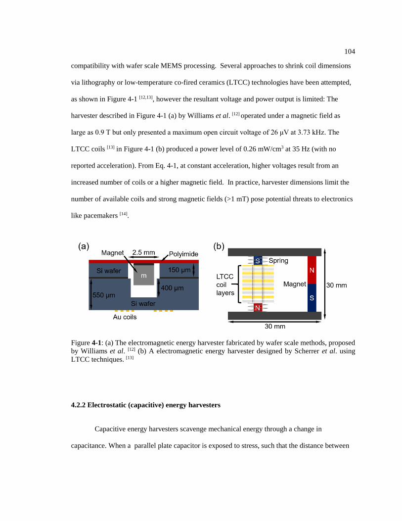
104
compatibility with wafer scale MEMS processing. Several approaches to shrink coil dimensions
via lithography or low-temperature co-fired ceramics (LTCC) technologies have been attempted,
as shown in Figure 4-1 [12,13], however the resultant voltage and power output is limited: The
harvester described in Figure 4-1 (a) by Williams et al. [12] operated under a magnetic field as
large as 0.9 T but only presented a maximum open circuit voltage of 26 μV at 3.73 kHz. The
LTCC coils [13] in Figure 4-1 (b) produced a power level of 0.26 mW/cm3 at 35 Hz (with no
reported acceleration). From Eq. 4-1, at constant acceleration, higher voltages result from an
increased number of coils or a higher magnetic field. In practice, harvester dimensions limit the
number of available coils and strong magnetic fields (>1 mT) pose potential threats to electronics
like pacemakers [14].
4.2.2 Electrostatic (capacitive) energy harvesters
Capacitive energy harvesters scavenge mechanical energy through a change in
capacitance. When a parallel plate capacitor is exposed to stress, such that the distance between
Figure 4-1: (a) The electromagnetic energy harvester fabricated by wafer scale methods, proposed
by Williams et al. [12] (b) A electromagnetic energy harvester designed by Scherrer et al. using
LTCC techniques. [13]
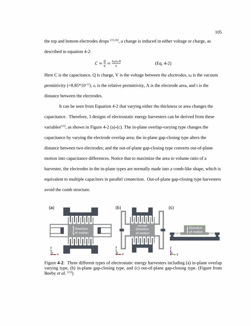
105
the top and bottom electrodes drops [15,16], a change is induced in either voltage or charge, as
described in equation 4-2:
𝐶 =𝑄
𝑉= 0 𝑟𝐴
𝑡 (Eq. 4-2)
Here C is the capacitance, Q is charge, V is the voltage between the electrodes, ε0 is the vacuum
permittivity (=8.85*10-12), εr is the relative permittivity, A is the electrode area, and t is the
distance between the electrodes.
It can be seen from Equation 4-2 that varying either the thickness or area changes the
capacitance. Therefore, 3 designs of electrostatic energy harvesters can be derived from these
variables[15], as shown in Figure 4-2 (a)-(c). The in-plane overlap-varying type changes the
capacitance by varying the electrode overlap area; the in-plane gap-closing type alters the
distance between two electrodes; and the out-of-plane gap-closing type converts out-of-plane
motion into capacitance differences. Notice that to maximize the area to volume ratio of a
harvester, the electrodes in the in-plane types are normally made into a comb-like shape, which is
equivalent to multiple capacitors in parallel connection. Out-of-plane gap-closing type harvesters
avoid the comb structure.
Figure 4-2: Three different types of electrostatic energy harvesters including (a) in-plane overlap
varying type, (b) in-plane gap-closing type, and (c) out-of-plane gap-closing type. (Figure from
Beeby et al. [15])
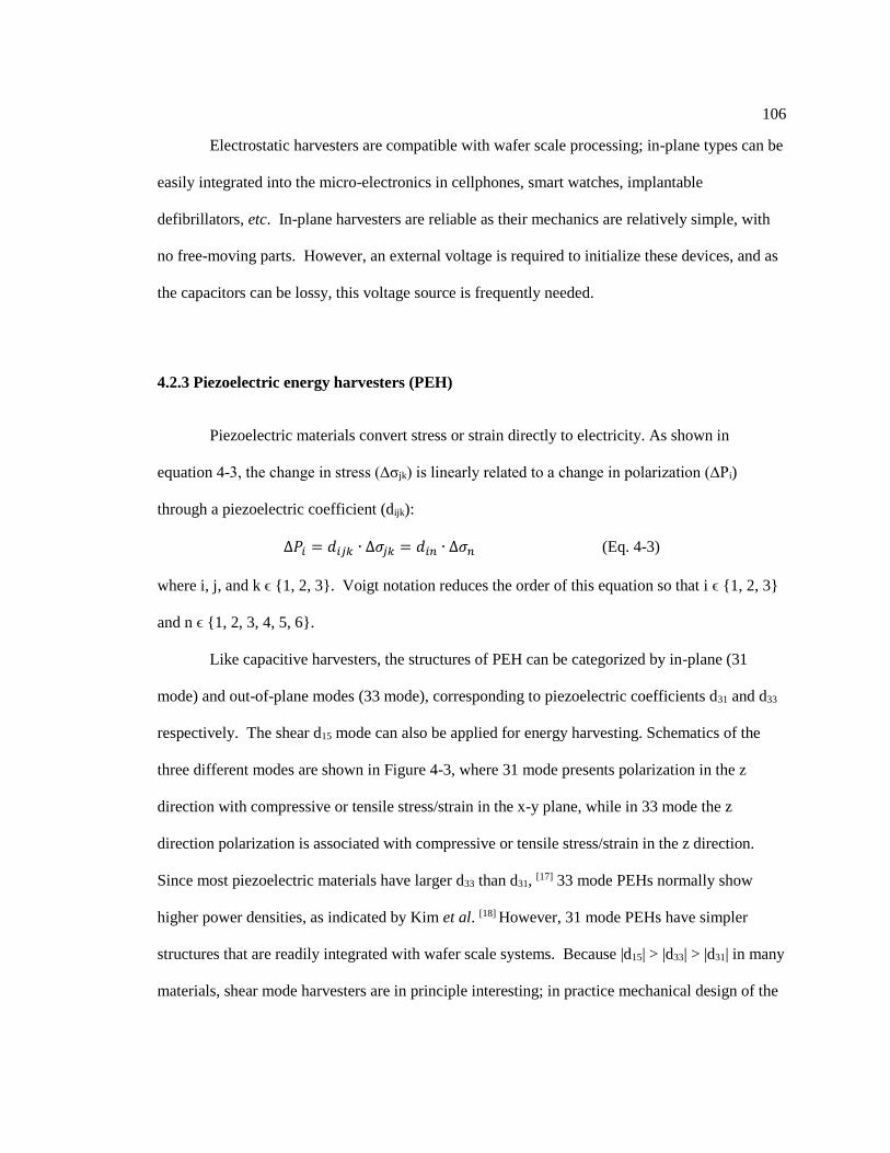
106
Electrostatic harvesters are compatible with wafer scale processing; in-plane types can be
easily integrated into the micro-electronics in cellphones, smart watches, implantable
defibrillators, etc. In-plane harvesters are reliable as their mechanics are relatively simple, with
no free-moving parts. However, an external voltage is required to initialize these devices, and as
the capacitors can be lossy, this voltage source is frequently needed.
4.2.3 Piezoelectric energy harvesters (PEH)
Piezoelectric materials convert stress or strain directly to electricity. As shown in
equation 4-3, the change in stress (∆σjk) is linearly related to a change in polarization (∆Pi)
through a piezoelectric coefficient (dijk):
∆𝑃𝑖 = 𝑑𝑖𝑗𝑘 ∙ ∆𝜎𝑗𝑘 = 𝑑𝑖𝑛 ∙ ∆𝜎𝑛 (Eq. 4-3)
where i, j, and k ϵ {1, 2, 3}. Voigt notation reduces the order of this equation so that i ϵ {1, 2, 3}
and n ϵ {1, 2, 3, 4, 5, 6}.
Like capacitive harvesters, the structures of PEH can be categorized by in-plane (31
mode) and out-of-plane modes (33 mode), corresponding to piezoelectric coefficients d31 and d33
respectively. The shear d15 mode can also be applied for energy harvesting. Schematics of the
three different modes are shown in Figure 4-3, where 31 mode presents polarization in the z
direction with compressive or tensile stress/strain in the x-y plane, while in 33 mode the z
direction polarization is associated with compressive or tensile stress/strain in the z direction.
Since most piezoelectric materials have larger d33 than d31, [17] 33 mode PEHs normally show
higher power densities, as indicated by Kim et al. [18] However, 31 mode PEHs have simpler
structures that are readily integrated with wafer scale systems. Because |d15| > |d33| > |d31| in many
materials, shear mode harvesters are in principle interesting; in practice mechanical design of the
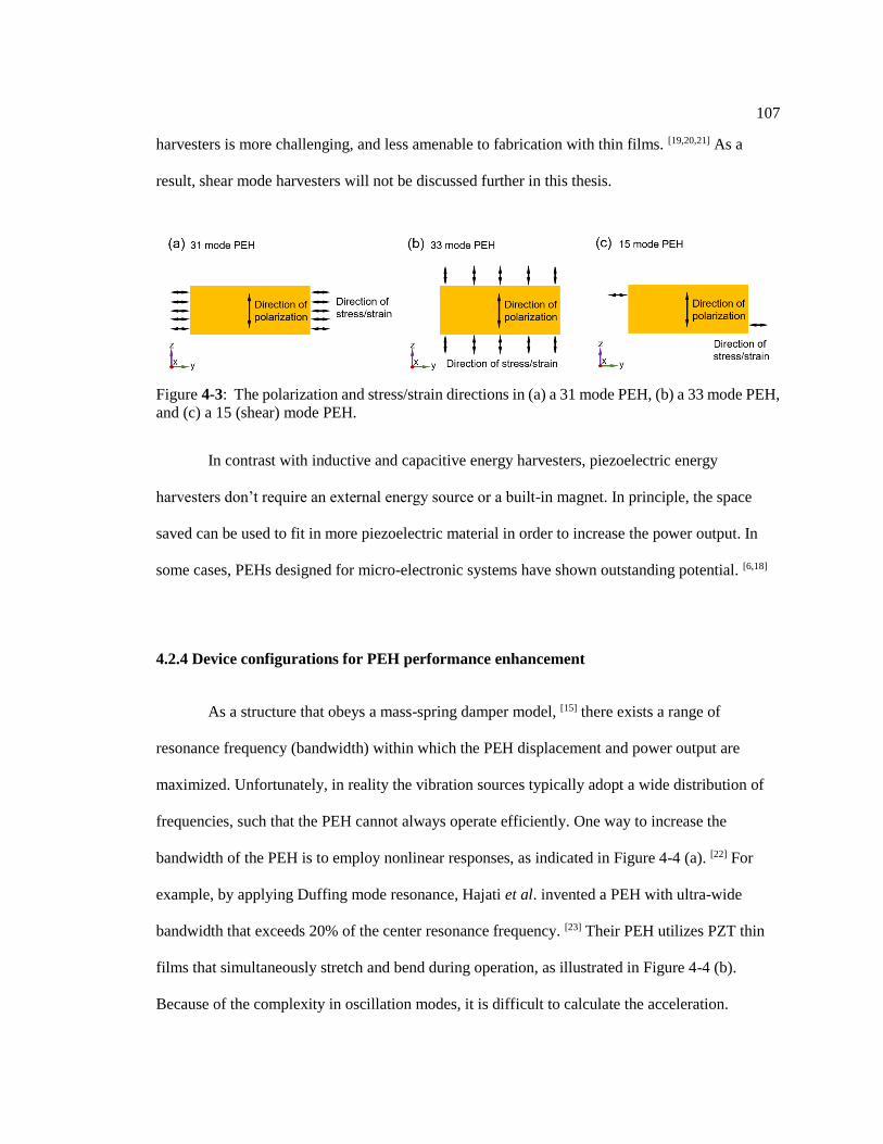
107
harvesters is more challenging, and less amenable to fabrication with thin films. [19,20,21] As a
result, shear mode harvesters will not be discussed further in this thesis.
In contrast with inductive and capacitive energy harvesters, piezoelectric energy
harvesters don’t require an external energy source or a built-in magnet. In principle, the space
saved can be used to fit in more piezoelectric material in order to increase the power output. In
some cases, PEHs designed for micro-electronic systems have shown outstanding potential. [6,18]
4.2.4 Device configurations for PEH performance enhancement
As a structure that obeys a mass-spring damper model, [15] there exists a range of
resonance frequency (bandwidth) within which the PEH displacement and power output are
maximized. Unfortunately, in reality the vibration sources typically adopt a wide distribution of
frequencies, such that the PEH cannot always operate efficiently. One way to increase the
bandwidth of the PEH is to employ nonlinear responses, as indicated in Figure 4-4 (a). [22] For
example, by applying Duffing mode resonance, Hajati et al. invented a PEH with ultra-wide
bandwidth that exceeds 20% of the center resonance frequency. [23] Their PEH utilizes PZT thin
films that simultaneously stretch and bend during operation, as illustrated in Figure 4-4 (b).
Because of the complexity in oscillation modes, it is difficult to calculate the acceleration.
Figure 4-3: The polarization and stress/strain directions in (a) a 31 mode PEH, (b) a 33 mode PEH,
and (c) a 15 (shear) mode PEH.
108
Nevertheless, the PEH presented a power density of 2 W/cm3, more than 2 orders of magnitude
higher than the PEH reviewed in the work by Beeby et al., if we assume the Duffing harvester
always operates on the most efficient branch of the curve in Figure 4-4 (a). [15] Additionally,
bistable and tristable PEH have also demonstrated outstanding capabilities to scavenge ambient
vibrations distributed over a wide frequency range. [24,25]
Increasing the magnitude of the strain also yields higher levels of harvested energy.
However, it is important that this be done without inducing excessive strain concentrations. For
example, Roundy et al. found that conventional rectangular-shaped cantilever harvesters
experience stress accumulation near the clamping site. At high accelerations, this can cause crack
initiation; [26] trapezoidal beams at least partially alleviate this issue. [26] Shown in Figure 4-5, Ma
et al. designed a piezoelectric compliance mechanism (PCM) that improved strain uniformity in
cantilevers, allowing PEHs to work under larger average stresses without exceeding cracking
stresses near the cantilever root. [27] (001) textured bimorph PZT thin films on Ni foils using PCM
designs demonstrated an outstanding power density ~3.9 mWcm-3G-2. [28]
Figure 4-4: (a) The theoretical deflection vs increasing (green arrows) and decreasing (red arrows)
frequency of the Duffing PEH structure described in (b). (b) Schematic of a Duffing PEH
experiencing stretching and bending motions. (c) Experimental setup for the bistable pendulum
PEH. (Figure from Hajati et al. [23])
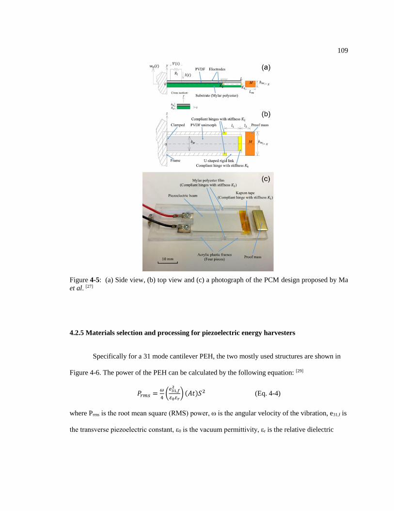
109
4.2.5 Materials selection and processing for piezoelectric energy harvesters
Specifically for a 31 mode cantilever PEH, the two mostly used structures are shown in
Figure 4-6. The power of the PEH can be calculated by the following equation: [29]
𝑃𝑟𝑚𝑠 =𝜔
4(𝑒31,𝑓
2
0 𝑟) (𝐴𝑡)𝑆2 (Eq. 4-4)
where Prms is the root mean square (RMS) power, ω is the angular velocity of the vibration, e31,f is
the transverse piezoelectric constant, ε0 is the vacuum permittivity, εr is the relative dielectric
Figure 4-5: (a) Side view, (b) top view and (c) a photograph of the PCM design proposed by Ma
et al. [27]
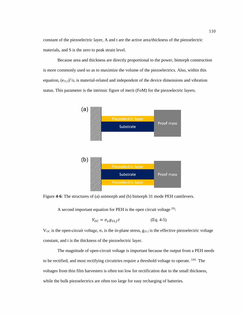
110
constant of the piezoelectric layer, A and t are the active area/thickness of the piezoelectric
materials, and S is the zero to peak strain level.
Because area and thickness are directly proportional to the power, bimorph construction
is more commonly used so as to maximize the volume of the piezoelectrics. Also, within this
equation, (e31,f)2/εr is material-related and independent of the device dimensions and vibration
status. This parameter is the intrinsic figure of merit (FoM) for the piezoelectric layers.
A second important equation for PEH is the open circuit voltage [9]:
𝑉𝑂𝐶 = 𝜎𝑥𝑔31,𝑓𝑡 (Eq. 4-5)
VOC is the open-circuit voltage, σx is the in-plane stress, g31,f is the effective piezoelectric voltage
constant, and t is the thickness of the piezoelectric layer.
The magnitude of open-circuit voltage is important because the output from a PEH needs
to be rectified, and most rectifying circuitries require a threshold voltage to operate. [30] The
voltages from thin film harvesters is often too low for rectification due to the small thickness,
while the bulk piezoelectrics are often too large for easy recharging of batteries.
Figure 4-6: The structures of (a) unimorph and (b) bimorph 31 mode PEH cantilevers.
111
In summary, a good PEH should at least have two characteristics:
I. The piezoelectric materials should have a large FoM.
II. The thickness of the piezoelectrics is neither too large nor too small.
Guided by the above two rules of thumb, a review of material systems for PEH
applications is presented.
4.2.5.1 Polymers
Piezoelectric polymers, such as polyvinylidene difluoride (PVDF) [31], polyurethane [32],
and cellulose [33], have the potentials to harvest vibration energy. Among them, PVDF and its
derivatives including polyvinylidene fluoride-trifluoro ethylene (PVDF-TrFE) [34] and
polyvinylidene dluoride-co-hexafluoropropylene (PVDF-HFP) [35] are more extensively studied
due to their superior piezoelectric charge coefficients (d33 and d31). This type of materials is
characterized by the low relative permittivity, normally below 20, [36] resulting in a large FoM.
The same reason also produces high piezoelectric voltage coefficients (g33 and g31). As a
consequence, the open circuit voltages of the polymeric PEH are generally very high. [37] In
addition, the outstanding flexibility has made piezoelectric polymers off the hook from
mechanical failure and suitable for high strain rate harvesters.
However, a major drawback of polymer piezoelectrics is the low power density. Cao et
al. reported a PVDF generator of power density ~1.94 mWG-2cm-3 under 100 Hz resonance
frequency. [38] Through optimization of device configuration of PVDF PEH, Song et al. achieved
a slightly higher power density of 3.44 mWcm-3G-2 at ~ 34 Hz. [37] This is because the resistivity
of the polymer is large enough that the current generated in the PEH is quite limited.
112
4.2.5.2 Single crystals
According to Neumann’s law [39], 21 of 32 point group symmetries have non-zero
piezoelectric constants. According to Neumann’s law. [39] One of the earliest known piezoelectric
single crystals is quartz. For α-quartz, the two non-zero piezoelectric constants are d11=2.29 pC/N
and d14=-0.680 pC/N, [40] both of which are too small for high power PEHs. Wurtzite ZnO single
crystals have an e33 of ~0.96 C/m2, an e31 of ~-0.62 C/m2, and an e15 of ~-0.37 C/m2. [41]
Numerous ZnO nano-wires have been used in miniature PEHs; these often produce small average
power levels due to the small volume of piezoelectric material. [42]
In recent years, the discovery of ferroelectric relaxor single crystals with high
piezoelectric coefficients, such as (1-x)Pb(Mg1/3Nb2/3O3)-xPbTiO3 (PMN-PT) [43], (1-
x)Pb(Zn1/3Nb2/3O3)-xPbTiO3 (PZN-PT) [44], and (1-x-y)Pb(In1/2Nb1/2)O3–xPb(Mg1/3Nb2/3)O3–
yPbTiO3 (PIN-PMN-PT) [45], has enabled the fabrication of high-power-density PEHs. For
instance, Yang et al. reported a cantilever PEH using PZN-PT single crystals that produced a
power density over 24 mWcm-3G-2, while a power density over 14 mWcm-3G-2 was reported for
device using PMN-PT single crystals. [46] Despite their outstanding piezoelectric coefficients,
relaxor single crystals have large relative permittivities; as a result the materials FoM is not very
high. Moreover, miniaturization of these materials without degrading the properties is difficult.
4.2.5.3 Ceramics
As piezoelectric ceramics are readily fabricated, they are widely utilized in PEHs. Most
ceramic powders are sintered at 50%-75% of their melting temperatures, production costs are
significantly smaller than single crystals of the same compositions. Not all piezoelectric ceramics
can be made into energy harvesters. For example, polycrystalline quartz does not show
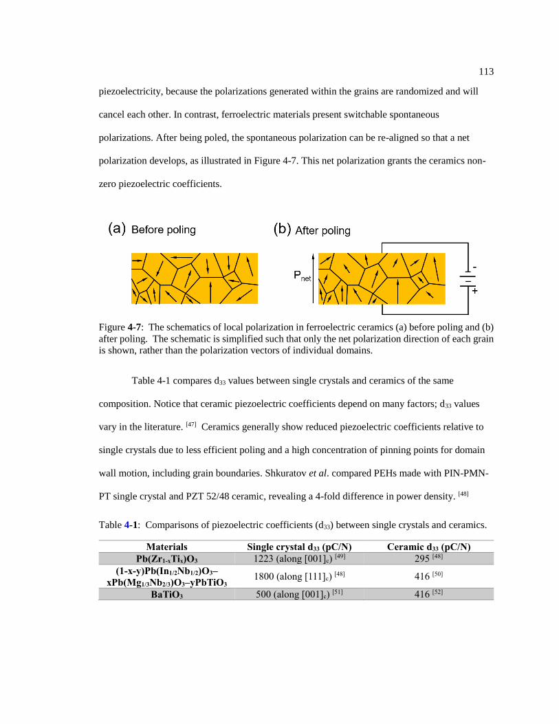
113
piezoelectricity, because the polarizations generated within the grains are randomized and will
cancel each other. In contrast, ferroelectric materials present switchable spontaneous
polarizations. After being poled, the spontaneous polarization can be re-aligned so that a net
polarization develops, as illustrated in Figure 4-7. This net polarization grants the ceramics non-
zero piezoelectric coefficients.
Table 4-1 compares d33 values between single crystals and ceramics of the same
composition. Notice that ceramic piezoelectric coefficients depend on many factors; d33 values
vary in the literature. [47] Ceramics generally show reduced piezoelectric coefficients relative to
single crystals due to less efficient poling and a high concentration of pinning points for domain
wall motion, including grain boundaries. Shkuratov et al. compared PEHs made with PIN-PMN-
PT single crystal and PZT 52/48 ceramic, revealing a 4-fold difference in power density. [48]
Figure 4-7: The schematics of local polarization in ferroelectric ceramics (a) before poling and (b)
after poling. The schematic is simplified such that only the net polarization direction of each grain
is shown, rather than the polarization vectors of individual domains.
Table 4-1: Comparisons of piezoelectric coefficients (d33) between single crystals and ceramics.
Materials Single crystal d33 (pC/N) Ceramic d33 (pC/N)
Pb(Zr1-xTix)O3 1223 (along [001]c) [49] 295 [48]
(1-x-y)Pb(In1/2Nb1/2)O3–
xPb(Mg1/3Nb2/3)O3–yPbTiO3 1800 (along [111]c) [48] 416 [50]
BaTiO3 500 (along [001]c) [51] 416 [52]
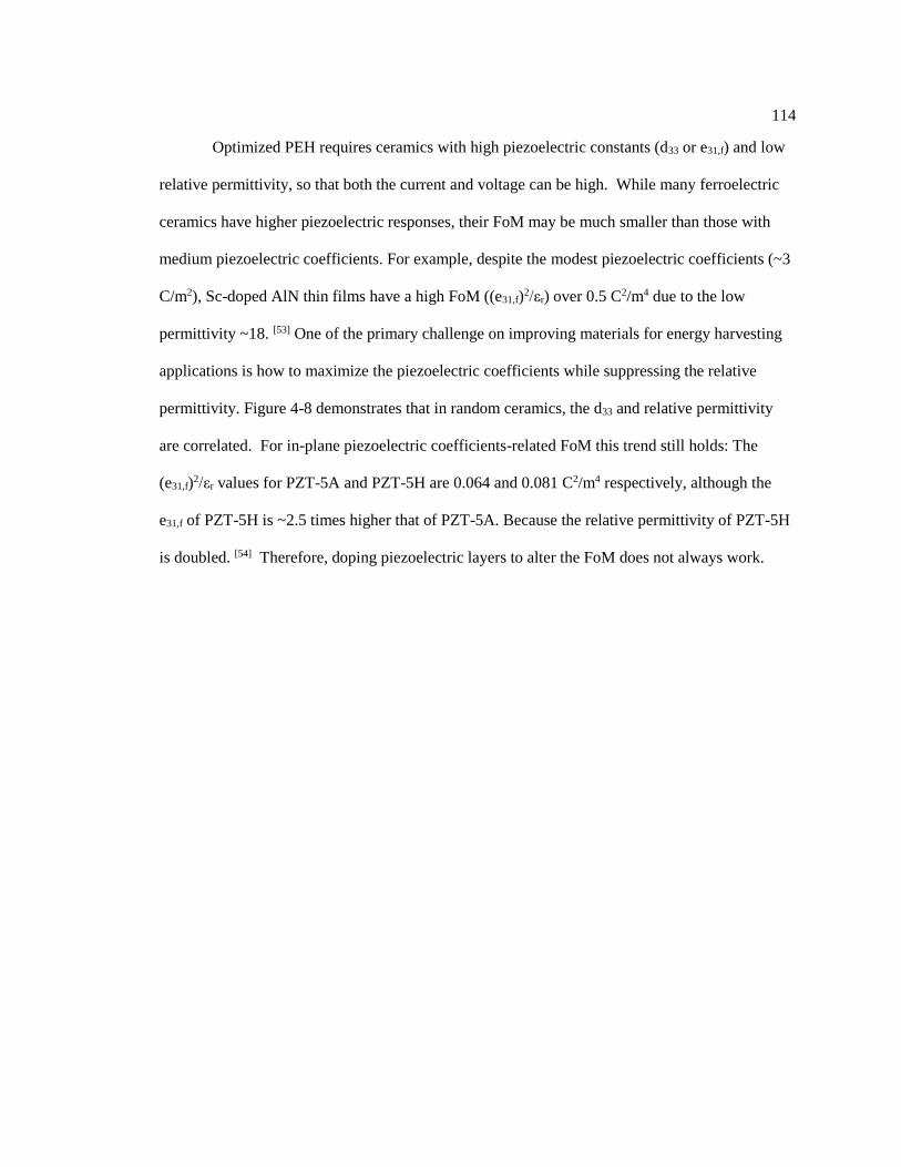
114
Optimized PEH requires ceramics with high piezoelectric constants (d33 or e31,f) and low
relative permittivity, so that both the current and voltage can be high. While many ferroelectric
ceramics have higher piezoelectric responses, their FoM may be much smaller than those with
medium piezoelectric coefficients. For example, despite the modest piezoelectric coefficients (~3
C/m2), Sc-doped AlN thin films have a high FoM ((e31,f)2/εr) over 0.5 C2/m4 due to the low
permittivity ~18. [53] One of the primary challenge on improving materials for energy harvesting
applications is how to maximize the piezoelectric coefficients while suppressing the relative
permittivity. Figure 4-8 demonstrates that in random ceramics, the d33 and relative permittivity
are correlated. For in-plane piezoelectric coefficients-related FoM this trend still holds: The
(e31,f)2/εr values for PZT-5A and PZT-5H are 0.064 and 0.081 C2/m4 respectively, although the
e31,f of PZT-5H is ~2.5 times higher that of PZT-5A. Because the relative permittivity of PZT-5H
is doubled. [54] Therefore, doping piezoelectric layers to alter the FoM does not always work.
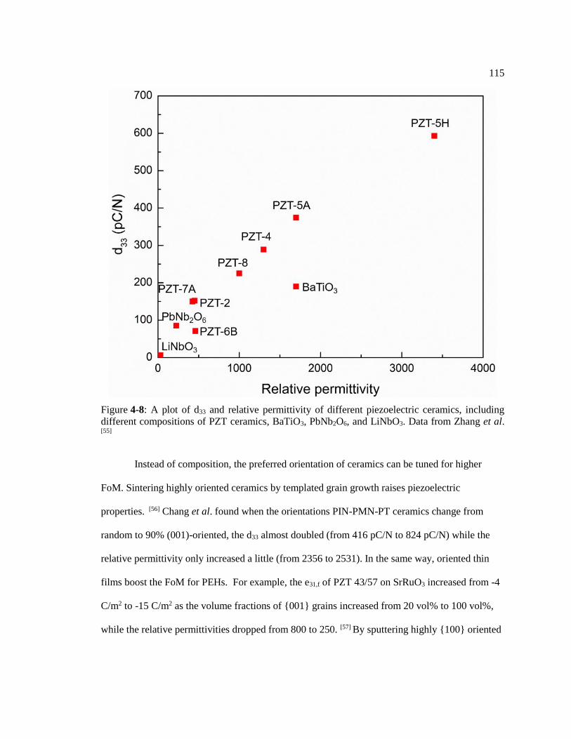
115
Instead of composition, the preferred orientation of ceramics can be tuned for higher
FoM. Sintering highly oriented ceramics by templated grain growth raises piezoelectric
properties. [56] Chang et al. found when the orientations PIN-PMN-PT ceramics change from
random to 90% (001)-oriented, the d33 almost doubled (from 416 pC/N to 824 pC/N) while the
relative permittivity only increased a little (from 2356 to 2531). In the same way, oriented thin
films boost the FoM for PEHs. For example, the e31,f of PZT 43/57 on SrRuO3 increased from -4
C/m2 to -15 C/m2 as the volume fractions of {001} grains increased from 20 vol% to 100 vol%,
while the relative permittivities dropped from 800 to 250. [57] By sputtering highly {100} oriented
Figure 4-8: A plot of d33 and relative permittivity of different piezoelectric ceramics, including
different compositions of PZT ceramics, BaTiO3, PbNb2O6, and LiNbO3. Data from Zhang et al. [55]
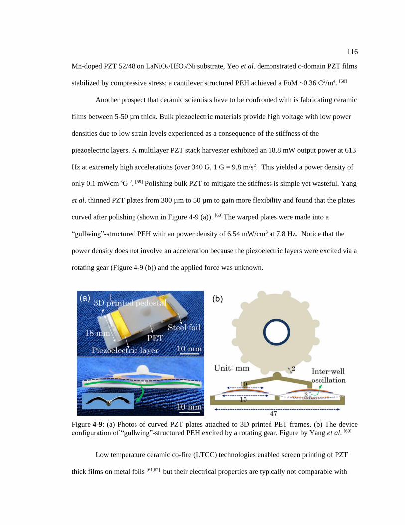
116
Mn-doped PZT 52/48 on LaNiO3/HfO2/Ni substrate, Yeo et al. demonstrated c-domain PZT films
stabilized by compressive stress; a cantilever structured PEH achieved a FoM ~0.36 C2/m4. [58]
Another prospect that ceramic scientists have to be confronted with is fabricating ceramic
films between 5-50 µm thick. Bulk piezoelectric materials provide high voltage with low power
densities due to low strain levels experienced as a consequence of the stiffness of the
piezoelectric layers. A multilayer PZT stack harvester exhibited an 18.8 mW output power at 613
Hz at extremely high accelerations (over 340 G, 1 G = 9.8 m/s2. This yielded a power density of
only 0.1 mWcm-3G-2. [59] Polishing bulk PZT to mitigate the stiffness is simple yet wasteful. Yang
et al. thinned PZT plates from 300 µm to 50 µm to gain more flexibility and found that the plates
curved after polishing (shown in Figure 4-9 (a)). [60] The warped plates were made into a
“gullwing”-structured PEH with an power density of 6.54 mW/cm3 at 7.8 Hz. Notice that the
power density does not involve an acceleration because the piezoelectric layers were excited via a
rotating gear (Figure 4-9 (b)) and the applied force was unknown.
Low temperature ceramic co-fire (LTCC) technologies enabled screen printing of PZT
thick films on metal foils [61,62] but their electrical properties are typically not comparable with
Figure 4-9: (a) Photos of curved PZT plates attached to 3D printed PET frames. (b) The device
configuration of “gullwing”-structured PEH excited by a rotating gear. Figure by Yang et al. [60]
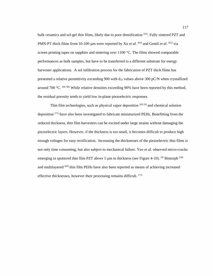
117
bulk ceramics and sol-gel thin films, likely due to poor densification [63]. Fully sintered PZT and
PMN-PT thick films from 10-100 µm were reported by Xu et al. [64] and Gentil et al. [65] via
screen printing tapes on sapphire and sintering over 1100 °C. The films showed comparable
performances as bulk samples, but have to be transferred to a different substrate for energy
harvester applications. A sol infiltration process for the fabrication of PZT thick films has
presented a relative permittivity exceeding 900 with d33 values above 300 pC/N when crystallized
around 700 °C. [66–68] While relative densities exceeding 90% have been reported by this method,
the residual porosity tends to yield low in-plane piezoelectric responses.
Thin film technologies, such as physical vapor deposition [69,70] and chemical solution
deposition [71] have also been investigated to fabricate miniaturized PEHs. Benefitting from the
reduced thickness, thin film harvesters can be excited under large strains without damaging the
piezoelectric layers. However, if the thickness is too small, it becomes difficult to produce high
enough voltages for easy rectification. Increasing the thicknesses of the piezoelectric thin films is
not only time consuming, but also subject to mechanical failure. Yeo et al. observed micro-cracks
emerging in sputtered thin film PZT above 5 µm in thickness (see Figure 4-10). [9] Bimorph [28]
and multilayered [69] thin film PEHs have also been reported as means of achieving increased
effective thicknesses, however their processing remains difficult. [72]
118
One of the principle goals of this work is to improve the mechanical and electrical
properties of the tape cast PZT thick films on metal substrates such that PEH can be further
optimized. This was attempted by adoption of cold sintering approaches to break the typical
thickness limitation imposed by standard film deposition methods, without sacrificing the film
density. In particular, the hope was that by densifying the films at low temperatures, films would
be less prone to mechanical failure due to thermal strains.
4.3 Experimental procedure
The fabrication of PZT/metal/PZT 2-2 composites, a common configuration for
cantilever PEH, can be divided into 3 phases: the preparation of PZT and substrates, the sintering
of PZT/metal/PZT composites, and the characterizations of sintered composites.
Figure 4-10: SEM showing (a) the microstructure and (b) micro-cracks on 5.4 µm thick PZT thin
films. Images from Yeo et al. [9]
119
4.3.1 Preparation of PZT tape, metal foils and Cu tapes
The PZT powder used for this experiment is PZT-5A (PKI-509, Piezo Kinetics, Inc.,
Bellefonte, PA) with a medium particle size of ~500 nm. The size distribution and the milling
procedures were described in the previous chapter. Before tape casting, 2 g PZT powder was
mixed with 0.2 g Pb(NO3)2 (Sigma-Aldrich Corp., St. Louis, MO) and 1.5 mL deionized water in
a mortar and pestle. The mixture was then dried in a box oven at 120 °C for 12 hours to remove
humidity. The tape cast recipe included two vehicles: vehicle A was composed of 95 wt% methyl
ethyl ketone (MEK, Alfa Aesar, Tewksbury, MA) and 5 wt% poly(propylene carbonate)
(QPAC®-40, Empower Materials, Inc., New Castle, DE); vehicle B consisted of 65 wt% MEK, 28
wt% QPAC®-40, and 7 wt% butyl benzyl phthalate (Santicizer-160, Tape Casting Warehouse,
Inc., Morrisville, PA). The dried PZT/Pb(NO3)2 powder was mixed with 1.38 g vehicle A, 1 g
MEK, and 0.68 g vehicle B with 1 min mixing between each step (Thinky Mixer AR-250,
Laguna Hills, CA). After de-foaming for 30 min, the slurry was tape cast on a Mylar sheet with a
blade height of ~8 mil (~203 µm). The as-cast tape was then air dried at room temperature for 10
min to remove MEK; and the final thickness of the dried tape was ~20 µm.
This work also explored the use of Ni foils, Ag foils and Cu foils as substrates for the
PZT films. Ni foils (25 µm, 99.99+%, Goodfellow Corporation, Coraopolis, PA) oxidize easily;
if the oxygen partial pressure during firing is low enough to retain metallic Ni, Pb is reduced.
LaNiO3/HfO2/Ni substrates were used to suppress the formation of NiO and reduce contact
between Ni and PZT. Here HfO2 was the passivation layer while LaNiO3 (LNO) served as the
bottom electrode. The processing details were similar to those described by Yeo et al. [71] except
that 100 nm HfO2 was deposited by atomic layer deposition at a rate of 0.93 Å/cycle. The silver
foils (25 µm, 99.9%, Sigma-Aldrich Corp., St. Louis, MO) were cut and laminated with PZT
120
tape. 5 layers of PbO thin film were spun cast on the surface of the Cu foils (25 µm, 99.8%, Alfa
Aesar, Tewksbury, MA), following procedures described by Coleman et al. [73]
In awareness of the constrained sintering issue of densifying PZT on metal foils, as an
alternative to the use of dense metal foils, tape cast Cu powder layers were also explored. The
tape casting procedures for Cu resembles that of the PZT tape: 6.70 g Cu (Shoei Chemical, Inc.,
Tokyo, Japan) were mixed with 5.5 g binder containing 20 vol% QPAC®-40 and 80 vol%
propylene carbonate. 0.4 mL MEK was added to the slurries in order to adjust the viscosity
before the slurries were homogenized in a mixer for 3 min. The mixtures were then tape cast on
Mylar sheets followed by baking in an oven at 80 °C for 5 hours to remove the solvent. The
thickness of the Cu tapes after drying was ~90 µm when the tapes were cast with a 13 mil doctor
blade height.
4.3.2 Cold sintering and co-firing of PZT/metal/PZT 2-2 composites
The PZT tape was cut into circular pieces one half-inch in diameter (~12.7 mm) and were
stacked in a PZT/metal/PZT sandwich structure, in which one layer of PZT tape was attached on
each side of the metal substrate. Lamination was done in a half-inch-diameter circular pressing
die at 50 MPa, 80 °C for 20 min [74]. The organics were then burnt out. For PZT on Ni or Ag
foils, the burn out took place in a box furnace under ambient conditions with a ramping rate of 0.4
°C/min to 275 °C, a hold time of 180 min, and a cooling rate of 5 °C/min. For PZT on Cu tapes,
a low pO2 furnace with dry nitrogen, wet nitrogen and forming gas (0.1 vol% H2 + 99.9 vol% N2)
flow (pO2 = 10-12 atm) was used. The temperature profile was the same as described above.
Following burn out, the samples were hung in a beaker half-filled with deionized water
heated to 80 °C for 60 min. Water vapor condenses on the sample and re-moistens the lead
nitrate; this is referred to as the “steaming” procedure. The stack was immediately cold sintered at
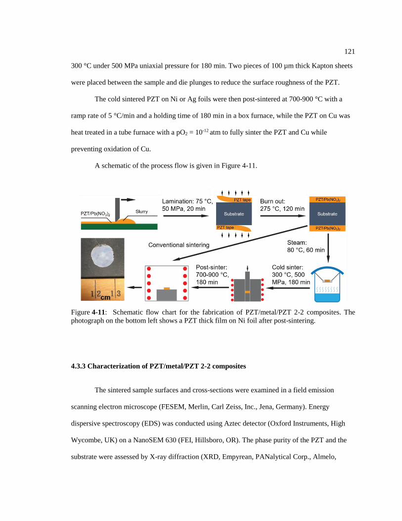
121
300 °C under 500 MPa uniaxial pressure for 180 min. Two pieces of 100 µm thick Kapton sheets
were placed between the sample and die plunges to reduce the surface roughness of the PZT.
The cold sintered PZT on Ni or Ag foils were then post-sintered at 700-900 °C with a
ramp rate of 5 °C/min and a holding time of 180 min in a box furnace, while the PZT on Cu was
heat treated in a tube furnace with a pO2 = 10-12 atm to fully sinter the PZT and Cu while
preventing oxidation of Cu.
A schematic of the process flow is given in Figure 4-11.
4.3.3 Characterization of PZT/metal/PZT 2-2 composites
The sintered sample surfaces and cross-sections were examined in a field emission
scanning electron microscope (FESEM, Merlin, Carl Zeiss, Inc., Jena, Germany). Energy
dispersive spectroscopy (EDS) was conducted using Aztec detector (Oxford Instruments, High
Wycombe, UK) on a NanoSEM 630 (FEI, Hillsboro, OR). The phase purity of the PZT and the
substrate were assessed by X-ray diffraction (XRD, Empyrean, PANalytical Corp., Almelo,
Figure 4-11: Schematic flow chart for the fabrication of PZT/metal/PZT 2-2 composites. The
photograph on the bottom left shows a PZT thick film on Ni foil after post-sintering.
122
Netherlands), using Cu Kα radiation from 2θ = 10° to 72° with a step size of 0.026° 2θ and a scan
rate of 0.067°/sec.
After processing, 2 mm diameter circular silver electrodes (Leitsiber 200, Ted Pella, Inc.,
Redding, CA) were painted on the sintered PZT, the permittivity-loss and polarization-electric
field (P-E) hysteresis loops were measured by an LCR meter (Hewlett-Packard 4284A, Agilent
Technologies, Inc., Palo Alto, CA) and a precision multiferroic analyzer (Radiant Technologies,
Inc., Albuquerque, NM), respectively. The P-E loops helped determine the coercive fields (Ec) of
the PZT films, which were then used to calculate the poling voltage. Samples were DC poled at
room temperature under 3-4 times Ec using a pA meter (Hewlett-Packard 4140B, Agilent
Technologies, Inc., Palo Alto, CA) for 20 min before piezoelectric coefficient (e31,f)
measurements. For all of the measurements, the high voltages were driven from the substrates
(bottom electrodes).
The e31,f measurements were carried out on a custom wafer flexure station [75]. The
specimens were glued on 4-inch silicon wafers, with strain gauges (gauge factor ~1.95, Omega
Engineering, Inc., Norwalk, CT) attached on top. Every measurement utilized two strain gauges
that were perpendicular to each other. The wafers were flexed at 4 Hz via a speaker controlled by
a lock-in amplifier (SR830, Stanford Research Systems, Sunnyvale, CA). A quarter Wheatstone
bridge was used to process the signals from the strain gauges while a charge integration circuit
collected the charges generated from the electrodes. The e31,f coefficient was calculated from [76]:
𝑒31,𝑓 =𝑄
𝐴(𝑥1+𝑥2) (Eq. 4-6)
where Q represents the charge generated from the electrode, A is the area of the electrode, and x1,
x2 are strains in two directions.
123
4.4 Results and discussion
4.4.1 PZT thick films on metal foils
In initial experiments, it was found that the burnt out PZT tapes collapsed either during
steaming or when loaded into the pressing die if the samples were hand-stacked without
lamination; this is likely related to the low green density and small thickness of the PZT tape.
This problem could be largely ameliorated by adding a lamination step before cold sintering.
Figure 4-12 (a)-(d) compares the 700 °C post-sintered PZT tapes on Ni foils with and without the
lamination process. Lamination did not change the film microstructure significantly but it greatly
suppressed the macro-flaws in the PZT layer.
A control sample was sintered at 700 °C without steaming and cold sintering to study the
effects of CSP on the PZT quality. As seen in Figure 4-12 (d)-(g), after post-sintering the cold
sintered sample presented mostly closed pores, suggesting a relative density over 92% [77], while
the conventionally sintered PZT tape was still in the initial stage of sintering. The cold sintered
tape was only a little over 10 µm thick. In contrast, for conventionally sintered PZT tape was 16
µm thick, consistent with its low density.
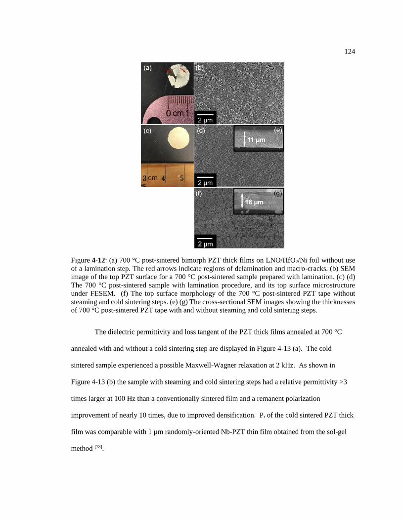
124
The dielectric permittivity and loss tangent of the PZT thick films annealed at 700 °C
annealed with and without a cold sintering step are displayed in Figure 4-13 (a). The cold
sintered sample experienced a possible Maxwell-Wagner relaxation at 2 kHz. As shown in
Figure 4-13 (b) the sample with steaming and cold sintering steps had a relative permittivity >3
times larger at 100 Hz than a conventionally sintered film and a remanent polarization
improvement of nearly 10 times, due to improved densification. Pr of the cold sintered PZT thick
film was comparable with 1 µm randomly-oriented Nb-PZT thin film obtained from the sol-gel
method [78].
Figure 4-12: (a) 700 °C post-sintered bimorph PZT thick films on LNO/HfO2/Ni foil without use
of a lamination step. The red arrows indicate regions of delamination and macro-cracks. (b) SEM
image of the top PZT surface for a 700 °C post-sintered sample prepared with lamination. (c) (d)
The 700 °C post-sintered sample with lamination procedure, and its top surface microstructure
under FESEM. (f) The top surface morphology of the 700 °C post-sintered PZT tape without
steaming and cold sintering steps. (e) (g) The cross-sectional SEM images showing the thicknesses
of 700 °C post-sintered PZT tape with and without steaming and cold sintering steps.
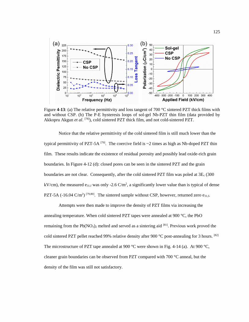
125
Notice that the relative permittivity of the cold sintered film is still much lower than the
typical permittivity of PZT-5A [79]. The coercive field is ~2 times as high as Nb-doped PZT thin
film. These results indicate the existence of residual porosity and possibly lead oxide-rich grain
boundaries. In Figure 4-12 (d): closed pores can be seen in the sintered PZT and the grain
boundaries are not clear. Consequently, after the cold sintered PZT film was poled at 3Ec (300
kV/cm), the measured e31,f was only -2.6 C/m2, a significantly lower value than is typical of dense
PZT-5A (-16.04 C/m2) [79,80]. The sintered sample without CSP, however, returned zero e31,f.
Attempts were then made to improve the density of PZT films via increasing the
annealing temperature. When cold sintered PZT tapes were annealed at 900 °C, the PbO
remaining from the Pb(NO3)2 melted and served as a sintering aid [81]. Previous work proved the
cold sintered PZT pellet reached 99% relative density after 900 °C post-annealing for 3 hours. [82]
The microstructure of PZT tape annealed at 900 °C were shown in Fig. 4-14 (a). At 900 °C,
cleaner grain boundaries can be observed from PZT compared with 700 °C anneal, but the
density of the film was still not satisfactory.
Figure 4-13: (a) The relative permittivity and loss tangent of 700 °C sintered PZT thick films with
and without CSP. (b) The P-E hysteresis loops of sol-gel Nb-PZT thin film (data provided by
Akkopru Akgun et al. [78]), cold sintered PZT thick film, and not cold-sintered PZT.
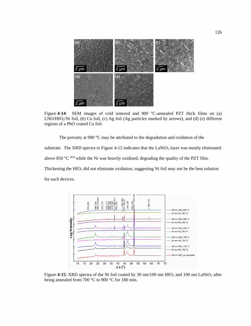
126
The porosity at 900 °C may be attributed to the degradation and oxidation of the
substrate. The XRD spectra in Figure 4-15 indicates that the LaNiO3 layer was mostly eliminated
above 850 °C [83] while the Ni was heavily oxidized, degrading the quality of the PZT film.
Thickening the HfO2 did not eliminate oxidation, suggesting Ni foil may not be the best solution
for such devices.
Figure 4-14: SEM images of cold sintered and 900 °C-annealed PZT thick films on (a)
LNO/HfO2/Ni foil, (b) Cu foil, (c) Ag foil (Ag particles marked by arrows), and (d) (e) different
regions of a PbO coated Cu foil.
Figure 4-15: XRD spectra of the Ni foil coated by 30 nm/100 nm HfO2 and 100 nm LaNiO3 after
being annealed from 700 °C to 900 °C for 180 min.
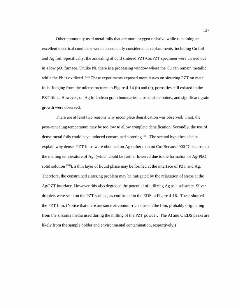
127
Other commonly used metal foils that are more oxygen resistive while remaining an
excellent electrical conductor were consequently considered as replacements, including Cu foil
and Ag foil. Specifically, the annealing of cold sintered PZT/Cu/PZT specimen were carried out
in a low pO2 furnace. Unlike Ni, there is a processing window where the Cu can remain metallic
while the Pb is oxidized. [84] These experiments exposed more issues on sintering PZT on metal
foils. Judging from the microstructures in Figure 4-14 (b) and (c), porosities still existed in the
PZT films. However, on Ag foil, clean grain boundaries, closed triple points, and significant grain
growth were observed.
There are at least two reasons why incomplete densification was observed. First, the
post-annealing temperature may be too low to allow complete densification. Secondly, the use of
dense metal foils could have induced constrained sintering [85]. The second hypothesis helps
explain why denser PZT films were obtained on Ag rather than on Cu: Because 900 °C is close to
the melting temperature of Ag, (which could be further lowered due to the formation of Ag-PbO
solid solution [86]), a thin layer of liquid phase may be formed at the interface of PZT and Ag.
Therefore, the constrained sintering problem may be mitigated by the relaxation of stress at the
Ag/PZT interface. However this also degraded the potential of utilizing Ag as a substrate. Silver
droplets were seen on the PZT surface, as confirmed in the EDS in Figure 4-16. These shorted
the PZT film. (Notice that there are some zirconium-rich sites on the film, probably originating
from the zirconia media used during the milling of the PZT powder. The Al and C EDS peaks are
likely from the sample holder and environmental contamination, respectively.)
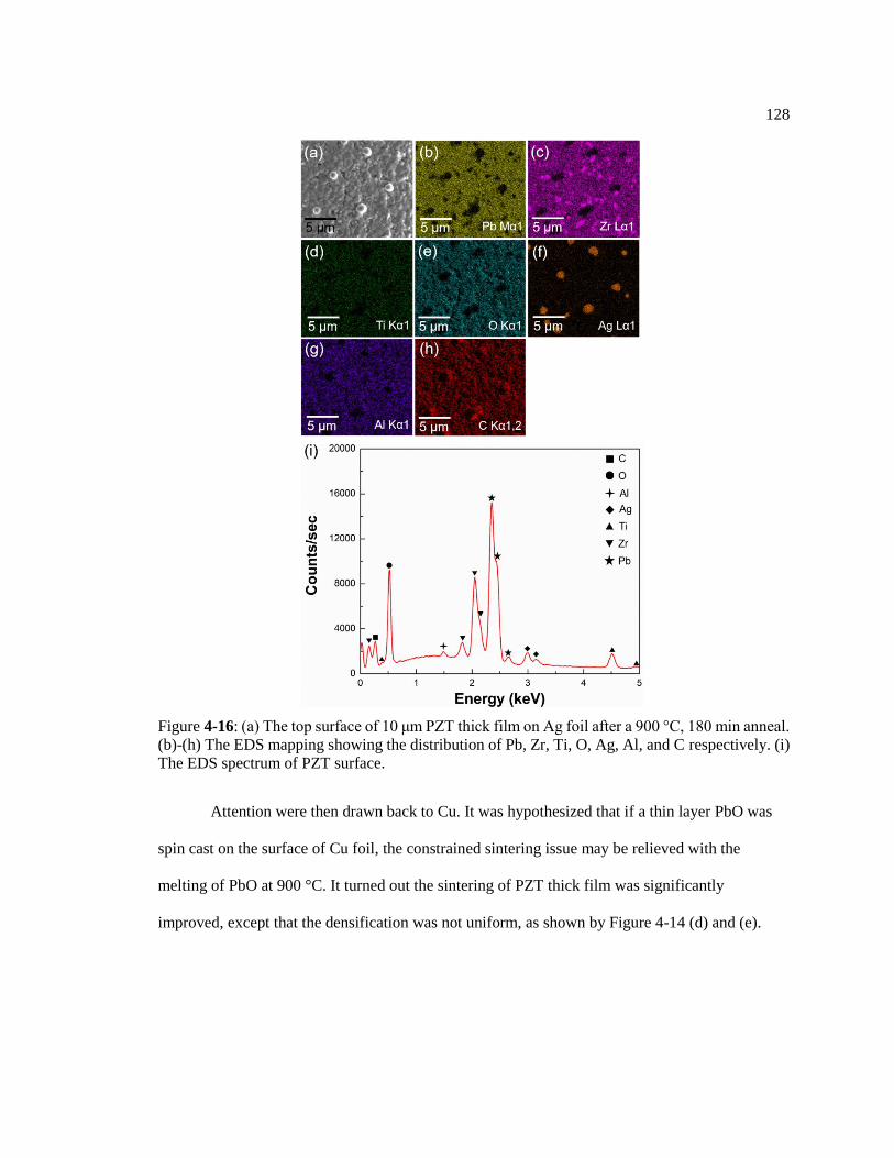
128
Attention were then drawn back to Cu. It was hypothesized that if a thin layer PbO was
spin cast on the surface of Cu foil, the constrained sintering issue may be relieved with the
melting of PbO at 900 °C. It turned out the sintering of PZT thick film was significantly
improved, except that the densification was not uniform, as shown by Figure 4-14 (d) and (e).
Figure 4-16: (a) The top surface of 10 μm PZT thick film on Ag foil after a 900 °C, 180 min anneal.
(b)-(h) The EDS mapping showing the distribution of Pb, Zr, Ti, O, Ag, Al, and C respectively. (i)
The EDS spectrum of PZT surface.

129
4.4.2 PZT thick films on tape cast Cu films
Based on the preliminary success of PZT sintering on PbO coated Cu foil, a second
approach to the avoidance of constrained sintering issue is the simultaneous densification of PZT
and the Cu substrate. Tape cast Cu thick films were laminated with PZT tapes and the rest of the
procedures remained unchanged. In practice, it was found that the burnt out PZT/Cu tape/PZT
structure is very fragile. PZT and Cu densification occurred during cold sintering, which
enhanced the strength of the composites. Figure 4-17 (a), (c), and (e) show a high compact
density of Cu and PZT after CSP, with a clean PZT-Cu interface.
Figure 4-17: (a) (b) Cross-sections of the PZT on Cu tape after CSP (left) and after 900 °C post-
sintering (right) showing PZT/Cu/PZT structures. (c) (d) Zoomed in cross sections of as-cold
sintered (left) and 800 °C post-sintered (right) samples emphasizing the PZT-Cu interface. (e) (f)
The top surfaces of the as-cold sintered (left) and 800 °C post-sintered (right) PZT films.

130
Dense PZT was acquired (Figure 4-17 (f)) after annealing at only 800 °C for 180 min in a
low pO2 furnace. This is presumably a result of good PZT and Cu compaction during CSP, and
the formation of a PbO-Cu2O eutectic melt [87]. It is noted that a PZT thick film without lead
nitrate failed to sinter under the same conditions (Figure C-1). The sintered Cu layer was 40 µm
thick, sandwiched between 10 µm bimorph PZT thick films, as seen in Figure 4-17 (b). Large
crystals appeared on the top surface of PZT. These are suggested by Figure C-2 and Figure C-3
to be Cu2O, which is probably from the contaminated sample holder and can be eliminated by
cleaning the sample holder before post-annealing. However, even after cleaning the sample
holder, there is still an interface between post-annealed PZT and Cu like the one shown in Figure
4-17 (d). According to Figure C-4, the interface consists of Cu and O. Figure 4-18 further
corroborated the existence of a Cu2O interface. The Cu2O interface might originate from the
oxidation of Cu following the decomposition of lead nitrate during burn out and cold sintering:
2𝑃𝑏(𝑁𝑂3)2 ⇌ 2𝑃𝑏𝑂 + 4𝑁𝑂2 + 𝑂2 (Eq. 4-7)
4𝐶𝑢 + 𝑂2 ⇌ 𝐶𝑢2𝑂 (Eq. 4-8)
The above reactions are likely to be more complex in practice as Figure 4-18 indicated
some unknown peaks at low angles in the as cold sintered samples. Although difficult to index,
these peaks must be from crystal structures with large lattice parameters, for example, lead
hydroxyl carbonates and lead hydroxyl nitrates. The oxidation of Cu occurs at the interface
between PZT and Cu, which is isolated from the external gas flow. This may explain why the
Cu2O layer cannot be removed even while processing in low pO2 conditions. The Cu2O intensity
drop above 600 °C anneal is possibly caused by the X-ray absorption in denser PZT, since Figure
C-5 showed that necking and grain growth appear at 600 °C. At this same temperature, PbO starts
to volatilize and most of it is eventually removed from the system.
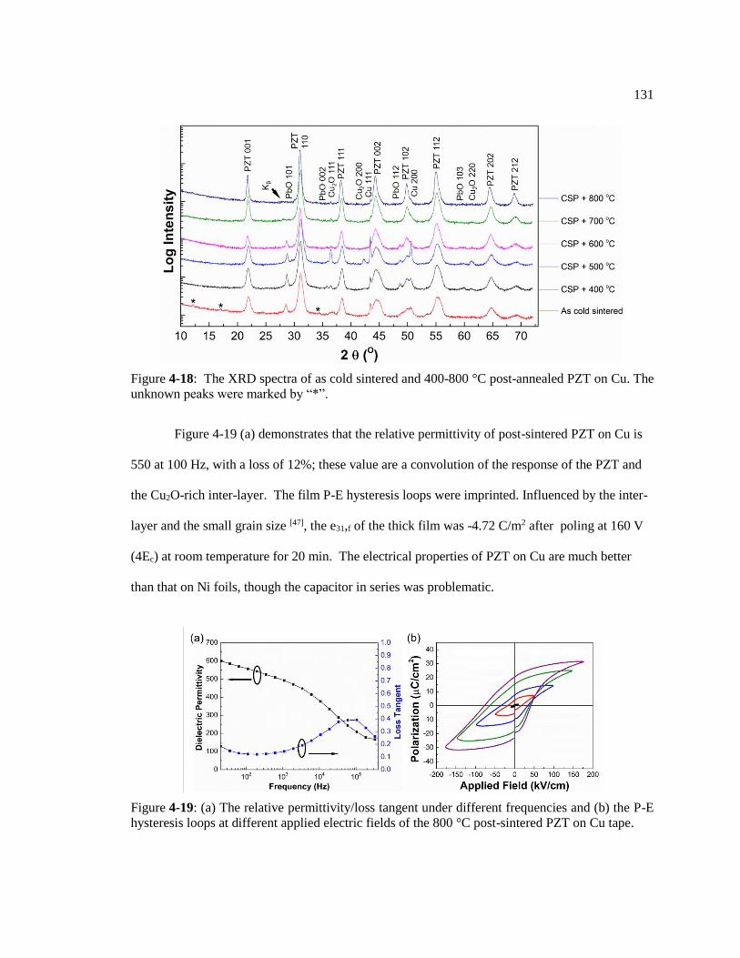
131
Figure 4-19 (a) demonstrates that the relative permittivity of post-sintered PZT on Cu is
550 at 100 Hz, with a loss of 12%; these value are a convolution of the response of the PZT and
the Cu2O-rich inter-layer. The film P-E hysteresis loops were imprinted. Influenced by the inter-
layer and the small grain size [47], the e31,f of the thick film was -4.72 C/m2 after poling at 160 V
(4Ec) at room temperature for 20 min. The electrical properties of PZT on Cu are much better
than that on Ni foils, though the capacitor in series was problematic.
Figure 4-18: The XRD spectra of as cold sintered and 400-800 °C post-annealed PZT on Cu. The
unknown peaks were marked by “*”.
Figure 4-19: (a) The relative permittivity/loss tangent under different frequencies and (b) the P-E
hysteresis loops at different applied electric fields of the 800 °C post-sintered PZT on Cu tape.
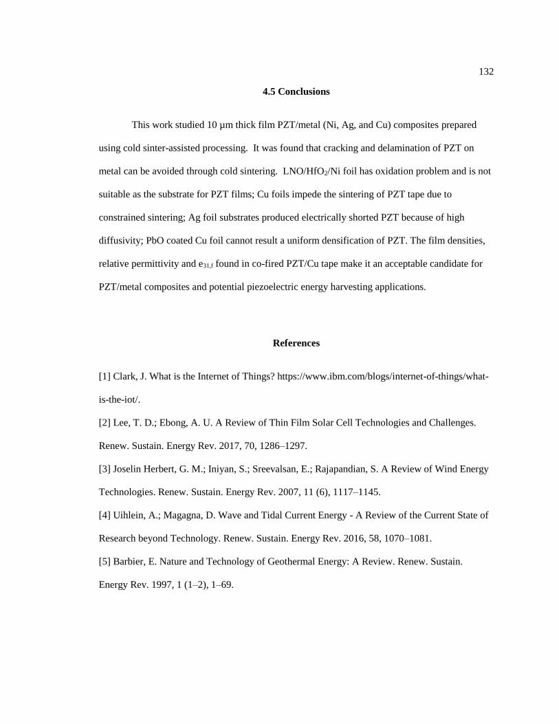
132
4.5 Conclusions
This work studied 10 µm thick film PZT/metal (Ni, Ag, and Cu) composites prepared
using cold sinter-assisted processing. It was found that cracking and delamination of PZT on
metal can be avoided through cold sintering. LNO/HfO2/Ni foil has oxidation problem and is not
suitable as the substrate for PZT films; Cu foils impede the sintering of PZT tape due to
constrained sintering; Ag foil substrates produced electrically shorted PZT because of high
diffusivity; PbO coated Cu foil cannot result a uniform densification of PZT. The film densities,
relative permittivity and e31,f found in co-fired PZT/Cu tape make it an acceptable candidate for
PZT/metal composites and potential piezoelectric energy harvesting applications.
References
[1] Clark, J. What is the Internet of Things? https://www.ibm.com/blogs/internet-of-things/what-
is-the-iot/.
[2] Lee, T. D.; Ebong, A. U. A Review of Thin Film Solar Cell Technologies and Challenges.
Renew. Sustain. Energy Rev. 2017, 70, 1286–1297.
[3] Joselin Herbert, G. M.; Iniyan, S.; Sreevalsan, E.; Rajapandian, S. A Review of Wind Energy
Technologies. Renew. Sustain. Energy Rev. 2007, 11 (6), 1117–1145.
[4] Uihlein, A.; Magagna, D. Wave and Tidal Current Energy - A Review of the Current State of
Research beyond Technology. Renew. Sustain. Energy Rev. 2016, 58, 1070–1081.
[5] Barbier, E. Nature and Technology of Geothermal Energy: A Review. Renew. Sustain.
Energy Rev. 1997, 1 (1–2), 1–69.
133
[6] Andosca, R.; McDonald, T. G.; Genova, V.; Rosenberg, S.; Keating, J.; Benedixen, C.; Wu, J.
Experimental and Theoretical Studies on MEMS Piezoelectric Vibrational Energy Harvesters
with Mass Loading. Sensors Actuators A Phys. 2012, 178, 76–87.
[7] Dagdeviren, C.; Yang, B. D.; Su, Y.; Tran, P. L.; Joe, P.; Anderson, E.; Xia, J.; Doraiswamy,
V.; Dehdashti, B.; Feng, X.; et al. Conformal Piezoelectric Energy Harvesting and Storage from
Motions of the Heart, Lung, and Diaphragm. Proc. Natl. Acad. Sci. U. S. A. 2014, 111 (5), 1927–
1932.
[8] Liu, H.; Zhong, J.; Lee, C.; Lee, S.-W.; Lin, L. A Comprehensive Review on Piezoelectric
Energy Harvesting Technology: Materials, Mechanisms, and Applications. Appl. Phys. Rev.
2018, 5 (4), 041306.
[9] Yeo, H. G. Mechanical Energy Harvesters Utilizing {001} Textured PZT Films on Flexible
Metal Foils, PhD thesis, the Pennsylvania State University, 2017.
[10] Lee, B. S.; Lin, S. C.; Wu, W. J.; Wang, X. Y.; Chang, P. Z.; Lee, C. K. Piezoelectric MEMS
Generators Fabricated with an Aerosol Deposition PZT Thin Film. J. Micromechanics
Microengineering 2009, 19 (6), 065014.
[11] Oishi, A.; Okumura, H.; Katsumura, H.; Kagata, H. The Power Generation Characteristics
and Durability of a Vibration Power Generation Device Using Piezoelectric Thick Film Formed
Directly by Screen Printing on a Stainless Steel Substrate. J. Phys. Conf. Ser. 2014, 557 (1),
012131.
[12] Williams, C. B.; Shearwood, C.; Harradine, M. A.; Mellor, P. H.; Birch, T. S.; Yates, R. B.
Development of an Electromagnetic Micro-Generator. IEEE Proc. - Circuits, Devices Syst.; IEEE
2001, 148 (6), 337.
[13] Scherrer, S.; Plumlee, D. G.; Moll, A. J. Energy Scavenging Device in LTCC Materials.
Proc. IEEE Workshop on Microelectronics and Electron Devices; IEEE 2005, 1, 77–78.
134
[14] Beinart, R.; Nazarian, S. Effects of External Electrical and Magnetic Fields on Pacemakers
and Defibrillators. Circulation 2013, 128 (25), 2799–2809.
[15] Beeby, S. P.; Tudor, M. J.; White, N. M. Energy Harvesting Vibration Sources for
Microsystems Applications. Meas. Sci. Technol. 2006, 17 (12), R175–R195.
[16] Thomson, G.; Yurchenko, D.; Val, D. V. Dielectric Elastomers for Energy Harvesting. In
Energy Harvesting; IntechOpen, 2018, 41–61.
[17] Yang, Z.; Zhou, S.; Zu, J.; Inman, D. High-Performance Piezoelectric Energy Harvesters and
Their Applications. Joule 2018, 2 (4), 642–697.
[18] Kim, S.-B.; Park, H.; Kim, S.-H.; Wikle, H. C.; Park, J.-H.; Kim, D.-J. Comparison of
MEMS PZT Cantilevers Based on d31 and d33 Modes for Vibration Energy Harvesting. J.
Microelectromechanical Syst. 2013, 22 (1), 26–33.
[19] Wang, D.-A.; Liu, N.-Z. A Shear Mode Piezoelectric Energy Harvester Based on a
Pressurized Water Flow. Sensors Actuators A Phys. 2011, 167 (2), 449–458.
[20] Zhao, J.; Zheng, X.; Zhou, L.; Zhang, Y.; Sun, J.; Dong, W.; Deng, S.; Peng, S. Investigation
of a d15 Mode PZT-51 Piezoelectric Energy Harvester with a Series Connection Structure. Smart
Mater. Struct. 2012, 21 (10), 105006.
[21] Kulkarni, V.; Ben-Mrad, R.; Prasad, S. E.; Nemana, S. A Shear-Mode Energy Harvesting
Device Based on Torsional Stresses. IEEE/ASME Trans. Mechatronics; IEEE 2014, 19 (3), 801–
807.
[22] Daqaq, M. F.; Masana, R.; Erturk, A.; Dane Quinn, D. On the Role of Nonlinearities in
Vibratory Energy Harvesting: A Critical Review and Discussion. Appl. Mech. Rev. 2014, 66 (4).
[23] Hajati, A.; Kim, S.-G. Ultra-Wide Bandwidth Piezoelectric Energy Harvesting. Appl. Phys.
Lett. 2011, 99 (8), 083105.
[24] Cottone, F.; Vocca, H.; Gammaitoni, L. Nonlinear Energy Harvesting. Phys. Rev. Lett. 2009,
102 (8), 080601.
135
[25] Zhou, S.; Cao, J.; Inman, D. J.; Lin, J.; Liu, S.; Wang, Z. Broadband Tristable Energy
Harvester: Modeling and Experiment Verification. Appl. Energy 2014, 133, 33–39.
[26] Roundy, S.; Leland, E. S.; Baker, J.; Carleton, E.; Reilly, E.; Lai, E.; Otis, B.; Rabaey, J. M.;
Sundararajan, V.; Wright, P. K. Improving Power Output for Vibration-Based Energy
Scavengers. IEEE Pervasive Comput. 2005, 4 (1), 28–36.
[27] Ma, X.; Yeo, H. G.; Rahn, C. D.; Trolier-McKinstry, S. Efficient and Sensitive Energy
Harvesting Using Piezoelectric MEMS Compliant Mechanisms. In Volume 8: 27th Conference
on Mechanical Vibration and Noise; American Society of Mechanical Engineers, 2015; pp 1–12.
[28] Yeo, H. G.; Ma, X.; Rahn, C.; Trolier-McKinstry, S. Efficient Piezoelectric Energy
Harvesters Utilizing (001) Textured Bimorph PZT Films on Flexible Metal Foils. Adv. Funct.
Mater. 2016, 26 (32), 5940–5946.
[29] Xue, T. Energy Harvesting from Human Motion Using Eccentric Rotor-Based Generators
with Piezoelectric Transducers, PhD Thesis, University of Utah, 2018.
[30] Meng, M.; Ibrahim, A.; Xue, T.; Yeo, H. G.; Wang, D.; Roundy, S.; Trolier-McKinstry, S.;
Kiani, M. Multi-Beam Shared-Inductor Reconfigurable Voltage/SECE-Mode Piezoelectric
Energy Harvesting of Multi-Axial Human Motion. Proc. 2019 IEEE International Solid- State
Circuits Conference - (ISSCC) ; IEEE 2019, 3, 426–428.
[31] Gomes, J.; Serrado Nunes, J.; Sencadas, V.; Lanceros-Mendez, S. Influence of the β-Phase
Content and Degree of Crystallinity on the Piezo- and Ferroelectric Properties of Poly(Vinylidene
Fluoride). Smart Mater. Struct. 2010, 19 (6), 065010.
[32] Lebrun, L.; Guyomar, D.; Guiffard, B.; Cottinet, P.-J.; Putson, C. The Characterization of the
Harvesting Capabilities of an Electrostrictive Polymer Composite. Sensors Actuators A Phys.
2009, 153 (2), 251–257.
[33] Csoka, L.; Hoeger, I. C.; Rojas, O. J.; Peszlen, I.; Pawlak, J. J.; Peralta, P. N. Piezoelectric
Effect of Cellulose Nanocrystals Thin Films. ACS Macro Lett. 2012, 1 (7), 867–870.
136
[34] Omote, K.; Ohigashi, H.; Koga, K. Temperature Dependence of Elastic, Dielectric, and
Piezoelectric Properties of “single Crystalline’’ Films of Vinylidene Fluoride Trifluoroethylene
Copolymer. J. Appl. Phys. 1997, 81 (6), 2760–2769.
[35] Huan, Y.; Liu, Y.; Yang, Y. Simultaneous Stretching and Static Electric Field Poling of
Poly(Vinylidene Fluoride-Hexafluoropropylene) Copolymer Films. Polym. Eng. Sci. 2007, 47
(10), 1630–1633.
[36] Mishra, S.; Unnikrishnan, L.; Nayak, S. K.; Mohanty, S. Advances in Piezoelectric Polymer
Composites for Energy Harvesting Applications: A Systematic Review. Macromol. Mater. Eng.
2019, 304 (1), 1800463.
[37] Song, J.; Zhao, G.; Li, B.; Wang, J. Design Optimization of PVDF-Based Piezoelectric
Energy Harvesters. Heliyon 2017, 3 (9), e00377.
[38] Cao, Z.; Zhang, J.; Kuwano, H. Vibration Energy Harvesting Characterization of 1 cm2
Poly(Vinylidene Fluoride) Generators in Vacuum. Jpn. J. Appl. Phys. 2011, 50 (9), 09ND15.
[39] Newnham, R. E.; Trolier-McKinstry, S. Materials Engineering: Bonding, Structure, and
Structure-Property Relationships; Cambridge University Press, 2017.
[40] Cook, R. K.; Weissler, P. G. Piezoelectric Constants of Alpha- and Beta-Quartz at Various
Temperatures. Phys. Rev. 1950, 80 (4), 712–716.
[41] Kobiakov, I. B. Elastic, Piezoelectric and Dielectric Properties of ZnO and CdS Single
Crystals in a Wide Range of Temperatures. Solid State Commun. 1980, 35 (3), 305–310.
[42] Song, J.; Zhou, J.; Wang, Z. L. Piezoelectric and Semiconducting Coupled Power Generating
Process of a Single ZnO Belt/Wire. A Technology for Harvesting Electricity from the
Environment. Nano Lett. 2006, 6 (8), 1656–1662.
[43] Shrout, T. R.; Chang, Z. P.; Kim, N.; Markgraf, S. Dielectric Behavior of Single Crystals
near the (1−x)Pb(Mg1/3Nb2/3)O3-xPbTiO3 Morphotropic Phase Boundary. Ferroelectr. Lett. Sect.
1990, 12 (3), 63–69.
137
[44] Kuwata, J.; Uchino, K.; Nomura, S. Phase Transitions in the Pb(Zn1/3Nb2/3)O3-PbTiO3
System. Ferroelectrics 1981, 37 (1), 579–582.
[45] Li, F.; Zhang, S.; Xu, Z.; Wei, X.; Luo, J.; Shrout, T. R. Piezoelectric Activity of Relaxor-
PbTiO3 Based Single Crystals and Polycrystalline Ceramics at Cryogenic Temperatures: Intrinsic
and Extrinsic Contributions. Appl. Phys. Lett. 2010, 96 (19), 192903.
[46] Yang, Z.; Zu, J. Comparison of PZN-PT, PMN-PT Single Crystals and PZT Ceramic for
Vibration Energy Harvesting. Energy Convers. Manag. 2016, 122, 321–329.
[47] Randall, C. A.; Kim, N.; Kucera, J.-P.; Cao, W.; Shrout, T. R. Intrinsic and Extrinsic Size
Effects in Fine-Grained Morphotropic-Phase-Boundary Lead Zirconate Titanate Ceramics. J. Am.
Ceram. Soc. 2005, 81 (3), 677–688.
[48] Shkuratov, S. I.; Baird, J.; Antipov, V. G.; Talantsev, E. F.; Chase, J. B.; Hackenberger, W.;
Luo, J.; Jo, H. R.; Lynch, C. S. Ultrahigh Energy Density Harvested from Domain-Engineered
Relaxor Ferroelectric Single Crystals under High Strain Rate Loading. Sci. Rep. 2017, 7 (1),
46758.
[49] Xie, Y. Synthesis and Characterization of Piezo- / Ferroelectric Lead Zirconate-Titanate
(PZT) Single Crystals and Related Ternary Ceramics, PhD Thesis, Simon Fraser University,
2013.
[50] Chang, Y.; Wu, J.; Sun, Y.; Zhang, S.; Wang, X.; Yang, B.; Messing, G. L.; Cao, W.
Enhanced Electromechanical Properties and Phase Transition Temperatures in [001] Textured
Pb(In1/2Nb1/2)O3-Pb(Mg1/3Nb2/3)O3-PbTiO3 Ternary Ceramics. Appl. Phys. Lett. 2015, 107 (8),
082902.
[51] Park, S.-E.; Wada, S.; Cross, L. E.; Shrout, T. R. Crystallographically Engineered BaTiO3
Single Crystals for High-Performance Piezoelectrics. J. Appl. Phys. 1999, 86 (5), 2746–2750.
[52] Shen, Z.-Y.; Li, J.-F. Enhancement of Piezoelectric Constant d33 in BaTiO3 Ceramics Due to
Nano-Domain Structure. J. Ceram. Soc. Japan 2010, 118 (1382), 940–943.
138
[53] Akiyama, M.; Umeda, K.; Honda, A.; Nagase, T. Influence of Scandium Concentration on
Power Generation Figure of Merit of Scandium Aluminum Nitride Thin Films. Appl. Phys. Lett.
2013, 102 (2), 021915.
[54] Priya, S.; Inman, D. J. Energy Harvesting Technologies; Springer US, 2009.
[55] Zhang, S.; Li, F.; Jiang, X.; Kim, J.; Luo, J.; Geng, X. Advantages and Challenges of
Relaxor-PbTiO3 Ferroelectric Crystals for Electroacoustic Transducers – A Review. Prog. Mater.
Sci. 2015, 68, 1–66.
[56] Chang, Y.; Watson, B.; Fanton, M.; Meyer, R. J.; Messing, G. L. Enhanced Texture
Evolution and Piezoelectric Properties in CuO-Doped Pb(In1/2Nb1/2)O3-Pb(Mg1/3Nb2/3)O3-PbTiO3
Grain-Oriented Ceramics. Appl. Phys. Lett. 2017, 111 (23), 232901.
[57] Yeager, C. B.; Ehara, Y.; Oshima, N.; Funakubo, H.; Trolier-McKinstry, S. Dependence of
e31, f on Polar Axis Texture for Tetragonal Pb(ZrxTi1− x)O3 Thin Films. J. Appl. Phys. 2014, 116
(10), 104907.
[58] Yeo, H. G.; Xue, T.; Roundy, S.; Ma, X.; Rahn, C.; Trolier-McKinstry, S. Strongly (001)
Oriented Bimorph PZT Film on Metal Foils Grown by RF-Sputtering for Wrist-Worn
Piezoelectric Energy Harvesters. Adv. Funct. Mater. 2018, 28 (36), 1801327.
[59] Xu, T.-B.; Siochi, E. J.; Kang, J. H.; Zuo, L.; Zhou, W.; Tang, X.; Jiang, X. Energy
Harvesting Using a PZT Ceramic Multilayer Stack. Smart Mater. Struct. 2013, 22 (6), 1–15.
[60] Yang, B.; Yi, Z.; Tang, G.; Liu, J. A Gullwing-Structured Piezoelectric Rotational Energy
Harvester for Low Frequency Energy Scavenging. Appl. Phys. Lett. 2019, 115 (6), 063901.
[61] Lozinski, A.; Wang, F.; Uusimäki, A.; Leppävuori, S. PLZT Thick Films for Pyroelectric
Sensors. Meas. Sci. Technol. 1997, 8 (1), 33–37.
[62] Le Dren, S.; Simon, L.; Gonnard, P.; Troccaz, M.; Nicolas, A. Investigation of Factors
Affecting the Preparation of PZT Thick Films. Mater. Res. Bull. 2000, 35 (12), 2037–2045.
139
[63] Dorey, R. A.; Whatmore, R. W.; Beeby, S. P.; Torah, R. N.; White, N. M. Screen Printed
PZT Thick Films Using Composite Film Technology. Integr. Ferroelectr. 2003, 54 (1), 651–658.
[64] Baomin Xu; Buhler, S.; White, D.; Zesch, J.; Wong, W. Fabrication of Piezoelectric Thick
Films for High Frequency Transducers. In Transactions of the IEEE Symposium on Ultrasonics,
2003; IEEE, 2003; Vol. 2, pp 1999–2002.
[65] Gentil, S.; Damjanovic, D.; Setter, N. Pb(Mg1/3Nb2/3)O3 and (1 - X)Pb(Mg1/3Nb2/3)O3 -
XPbTiO3 Relaxor Ferroelectric Thick Films: Processing and Electrical Characterization. Journal
of Electroceramics. 2004, pp 151–161.
[66] Kwon, T. Y.; Park, J. H.; Kim, Y. B.; Yoon, D. S.; Cheon, C. Il; Lee, H. L.; Kim, T. S.
Preparation of Piezoelectric 0.1Pb(Zn0.5W0.5)O3–0.9Pb(Zr0.5Ti0.5)O3 Solid Solution and Thick
Films for Low Temperature Firing on a Si-Substrate. J. Cryst. Growth 2006, 295 (2), 172–178.
[67] Wu, D.; Zhou, Q.; Shung, K. K.; Bharadwaja, S. N.; Zhang, D.; Zheng, H. Dielectric and
Piezoelectric Properties of PZT Composite Thick Films with Variable Solution to Powder Ratios.
J. Am. Ceram. Soc. 2009, 92 (6), 1276–1279.
[68] Barrow, D. A.; Petroff, T. E.; Tandon, R. P.; Sayer, M. Characterization of Thick Lead
Zirconate Titanate Films Fabricated Using a New Sol Gel Based Process. J. Appl. Phys. 1997, 81
(2), 876–881.
[69] Kanda, K.; Hirai, S.; Fujita, T.; Maenaka, K. Piezoelectric MEMS with Multilayered
Pb(Zr,Ti)O3 Thin Films for Energy Harvesting. Sensors Actuators A Phys. 2018, 281, 229–235.
[70] Reilly, E. K.; Wright, P. K. Modeling, Fabrication and Stress Compensation of an Epitaxial
Thin Film Piezoelectric Microscale Energy Scavenging Device. J. Micromechanics
Microengineering 2009, 19 (9), 095014.
[71] Yeo, H. G.; Trolier-McKinstry, S. {001} Oriented Piezoelectric Films Prepared by Chemical
Solution Deposition on Ni Foils. J. Appl. Phys. 2014, 116 (1), 014105.
140
[72] Kim, S.-G.; Priya, S.; Kanno, I. Piezoelectric MEMS for Energy Harvesting. MRS Bull.
2012, 37 (11), 1039–1050.
[73] Coleman, K.; Walker, J.; Beechem, T.; Trolier-McKinstry, S. Effect of Stresses on the
Dielectric and Piezoelectric Properties of Pb(Zr0.52Ti0.48)O3 Thin Films. J. Appl. Phys. 2019, 126
(3), 034101.
[74] Gao, L.; Ko, S. W.; Guo, H.; Hennig, E.; Randall, C. A.; Jones, J. L. Demonstration of
Copper Co-Fired (Na,K)NbO3 Multilayer Structures for Piezoelectric Applications. J. Am.
Ceram. Soc. 2016, 99 (6), 2017–2023.
[75] Shepard, J. F.; Moses, P. J.; Trolier-McKinstry, S. The Wafer Flexure Technique for the
Determination of the Transverse Piezoelectric Coefficient (d31) of PZT Thin Films. Sensors
Actuators A Phys. 1998, 71 (1–2), 133–138.
[76] Garten, L. M.; Trolier-McKinstry, S. The Field Induced e31,f Piezoelectric and Rayleigh
Response in Barium Strontium Titanate Thin Films. Appl. Phys. Lett. 2014, 105 (13), 132905.
[77] Rahaman, M. N. Ceramic Processing and Sintering, 2nd ed.; Marcel Dekker: New York,
NY, 2003.
[78] Akkopru‐Akgun, B.; Zhu, W.; Lanagan, M. T.; Trolier‐McKinstry, S. The Effect of Imprint
on Remanent Piezoelectric Properties and Ferroelectric Aging of PbZr0.52Ti0.48O3 Thin Films. J.
Am. Ceram. Soc. 2019, 102 (9), 5328–5341.
[79] Erturk, A.; Inman, D. J. Piezoelectric Energy Harvesting; Lopes Junior, V., Steffen, V., Savi,
M. A., Eds.; John Wiley & Sons, Ltd: Chichester, UK, 2011.
[80] Dubois, M.-A.; Muralt, P. Measurement of the Effective Transverse Piezoelectric Coefficient
e31,f of AlN and Pb(Zrx,Ti1−x)O3 Thin Films. Sensors Actuators A Phys. 1999, 77 (2), 106–112.
[81] Atkin, R. B.; Fulrath, R. M. Point Defects and Sintering of Lead Zirconate-Titanate. J. Am.
Ceram. Soc. 1971, 54 (5), 265–270.
141
[82] Wang, D.; Guo, H.; Morandi, C. S.; Randall, C. A.; Trolier-McKinstry, S. Cold Sintering
and Electrical Characterization of Lead Zirconate Titanate Piezoelectric Ceramics. APL Mater.
2018, 6 (1), 016101.
[83] Li, A.; Ge, C.; Lü, P.; Ming, N. Preparation of Perovskite Conductive LaNiO3 Films by
Metalorganic Decomposition. Appl. Phys. Lett. 1996, 68 (10), 1347–1349.
[84] Gao, L.; Guo, H.; Zhang, S.; Randall, C. Base Metal Co-Fired Multilayer Piezoelectrics.
Actuators 2016, 5 (1), 8. PAGE RANGE?
[85] Holmes, P. J.; Loasby, R. G. Handbook of Thick Film Technology; Holmes, P. J., Loasby,
R. G., Eds.; Electrochemical Publications, 1976.
[86] Shao, Z. B.; Liu, K. R.; Liu, L. Q.; Liu, H. K.; Dou, S. Equilibrium Phase Diagrams in the
Systems PbO-Ag and CuO-Ag. J. Am. Ceram. Soc. 1993, 76 (10), 2663–2664.
[87] Corker, D. L.; Whatmore, R. W.; Ringgaard, E.; Wolny, W. W. Liquid-Phase Sintering of
PZT Ceramics. J. Eur. Ceram. Soc. 2000, 20 (12), 2039–2045.
Chapter 5
Conclusions and Future Work
5.1 Conclusions
BNO thin films are a potential candidate for energy storage devices on flexible substrates.
It was found that exposure of the amorphous films to a UV light source facilitated the removal of
organics. Benefiting from this, the BNO crystallization was initiated at a lower temperature (from
400 °C, 10 min to 375 °C, 10 min) and within shorter heat treatment duration (from 375 °C, 30
min to 375 °C, 10 min). Larger crystallite sizes were also indicated by the XRD peaks of UV-
treated BNO compared with not UV-treated samples under the same temperature profile. Due to
the elimination of carbon in the film through the UV treatment at an early stage, the film annealed
at 450 °C became less porous and achieved an energy density of 39 J/cm3 at room temperature at
10 kHz with an applied electric field of 3.6 MV/cm. The BNO thin films annealed at 350°C and
375°C, have shown lower energy storage densities but better temperature stability presumably
because of the extensive volume fraction of amorphous phase. When compared to other recently
developed materials, the BNO thin films are competitive due to their high energy densities and
relatively low processing temperatures.
PZT ceramics were cold sintered to >80% relative densities at 300 °C using bimodal PZT
powder with moisturized Pb(NO3)2 as a sintering aid. The underlying mechanism of PZT
densification during cold sintering is improved PZT particle packing induced by the plastic
deformation of the moist lead nitrate. Therefore, a viscous sintering model can be utilized to
explain the effects of temperature, pressure and time on the final pellet densities; the model
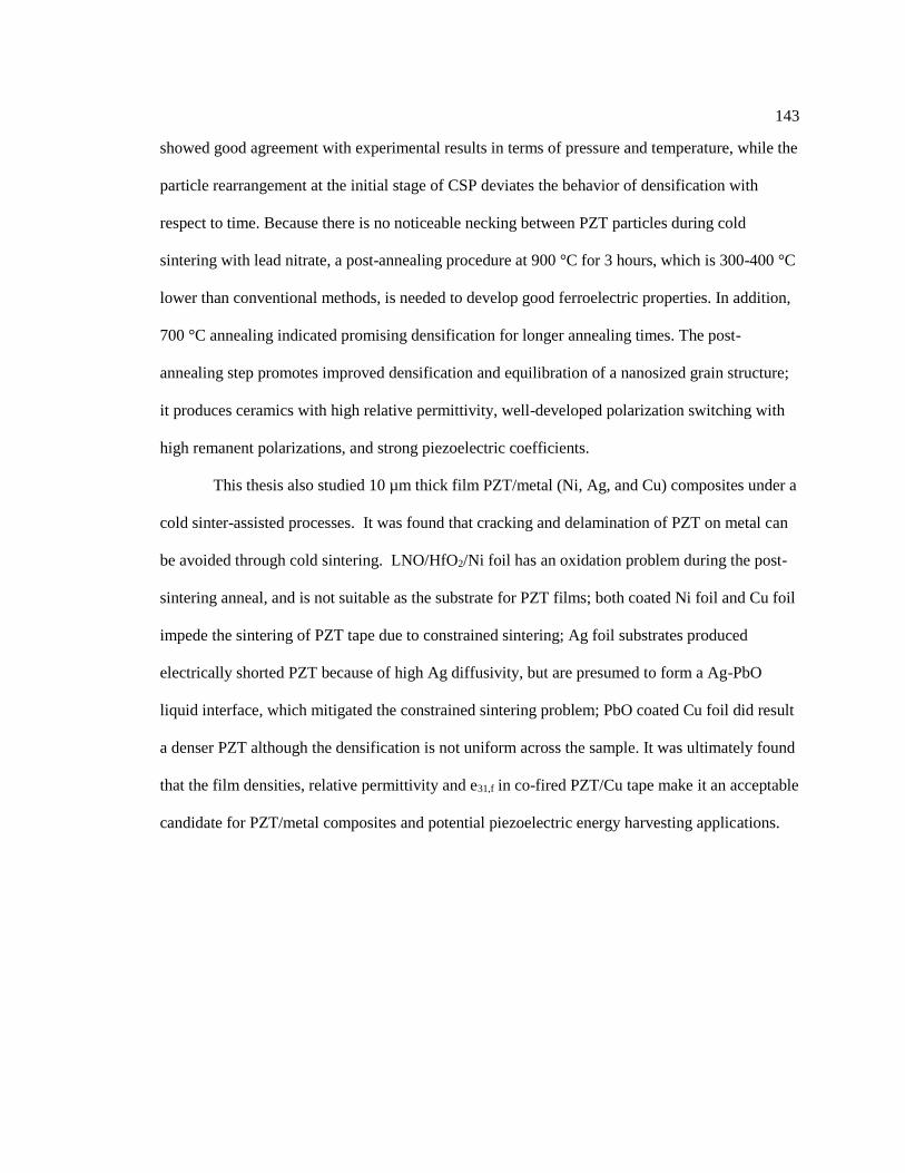
143
showed good agreement with experimental results in terms of pressure and temperature, while the
particle rearrangement at the initial stage of CSP deviates the behavior of densification with
respect to time. Because there is no noticeable necking between PZT particles during cold
sintering with lead nitrate, a post-annealing procedure at 900 °C for 3 hours, which is 300-400 °C
lower than conventional methods, is needed to develop good ferroelectric properties. In addition,
700 °C annealing indicated promising densification for longer annealing times. The post-
annealing step promotes improved densification and equilibration of a nanosized grain structure;
it produces ceramics with high relative permittivity, well-developed polarization switching with
high remanent polarizations, and strong piezoelectric coefficients.
This thesis also studied 10 µm thick film PZT/metal (Ni, Ag, and Cu) composites under a
cold sinter-assisted processes. It was found that cracking and delamination of PZT on metal can
be avoided through cold sintering. LNO/HfO2/Ni foil has an oxidation problem during the post-
sintering anneal, and is not suitable as the substrate for PZT films; both coated Ni foil and Cu foil
impede the sintering of PZT tape due to constrained sintering; Ag foil substrates produced
electrically shorted PZT because of high Ag diffusivity, but are presumed to form a Ag-PbO
liquid interface, which mitigated the constrained sintering problem; PbO coated Cu foil did result
a denser PZT although the densification is not uniform across the sample. It was ultimately found
that the film densities, relative permittivity and e31,f in co-fired PZT/Cu tape make it an acceptable
candidate for PZT/metal composites and potential piezoelectric energy harvesting applications.
144
5.2 Future work
5.2.1 Understanding the mechanisms of carbon elimination via deep ultra-violet treatment
The success of carbon removal via DUV exposure improved the energy storage
performance of BNO thin films. The underlying mechanism for this behavior was not discussed
extensively in the section 2.2; this portion of the future work provides a preliminary explanation
while indicating a few “loose ends” to further optimize the process.
First, the mechanisms of carbon elimination under DUV is believed to be related to the
decomposition of large organic molecules into smaller ones facilitated by the UV radiation.
Although, immediately after solution preparation, large organic molecules were not present, the
should be generated over time as a result of the esterification of ethylene glycol and citric acid
from the moment a bottle of solution was made. [1] As smaller molecules volatilize faster than
large ones for the same conditions, more carbon can be removed from the film either during DUV
exposure or the following secondary heat treatment. This is supported by the Fourier Transformed
Infrared (FTIR) spectra of bismuth zinc niobate tantalate (BZNT) thin films, as shown in Fig. 5-1.
Notice that the composition of the BZNT solution is almost the same as BNO solution, except
that there are zinc acetate and tantalum ethoxide precursors in BZNT. Before FTIR, two layers of
solution were spin cast on the wafer.
145
From the spectra, it is clear that considerable quantities of residual organics remain after
the 250 °C drying procedure. The peaks corresponding to residual organics can be effectively
suppressed by either pyrolyzing films on a hot plate at 350 °C for 10 min, or exposing the films
under UV for 3 min without hot plate heating (the film will still be heated up to ~150 °C by the
UV during the exposure). If a secondary heat treatment is applied after DUV exposure, when the
temperature is only 300 °C, the organics can almost be eliminated within the films, resulting an
FTIR spectrum similar to the wafer background. It is presumed that BNO films will behave in a
manner comparable to that of the BNZT, though a direct confirmation should be obtained in the
future.
It is also of interest to understand whether the carbon removal is dominated by UV
frequency, UV intensity, or the atmospheric environment. This topic has several technical
challenges including measuring the absorption spectrum of the solution, tuning the
wavelengths/intensities of the UV irradiation, etc. Therefore, the following discussion will only
offer a preliminary insight.
Figure 5-1: FTIR spectra of (lines from the top to bottom) BZNT film after spin casting and drying
at 250 °C for 3 min; after being dried and undergoing a 350 °C, 10 min pyrolysis without DUV
treatment; after being dried and UV exposed; and after being dried, exposed to the DUV treatment,
and subsequently pyrolyzed at 300 °C for 10 min. Shown for comparison is a platinized silicon
wafer with no BZNT film.
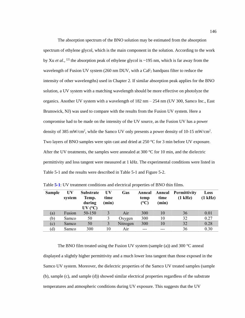
146
The absorption spectrum of the BNO solution may be estimated from the absorption
spectrum of ethylene glycol, which is the main component in the solution. According to the work
by Xu et al., [2] the absorption peak of ethylene glycol is ~195 nm, which is far away from the
wavelength of Fusion UV system (260 nm DUV, with a CaF2 bandpass filter to reduce the
intensity of other wavelengths) used in Chapter 2. If similar absorption peak applies for the BNO
solution, a UV system with a matching wavelength should be more effective on photolyze the
organics. Another UV system with a wavelength of 182 nm – 254 nm (UV 300, Samco Inc., East
Brunswick, NJ) was used to compare with the results from the Fusion UV system. Here a
compromise had to be made on the intensity of the UV source, as the Fusion UV has a power
density of 385 mW/cm2, while the Samco UV only presents a power density of 10-15 mW/cm2.
Two layers of BNO samples were spin cast and dried at 250 °C for 3 min before UV exposure.
After the UV treatments, the samples were annealed at 300 °C for 10 min, and the dielectric
permittivity and loss tangent were measured at 1 kHz. The experimental conditions were listed in
Table 5-1 and the results were described in Table 5-1 and Figure 5-2.
The BNO film treated using the Fusion UV system (sample (a)) and 300 °C anneal
displayed a slightly higher permittivity and a much lower loss tangent than those exposed in the
Samco UV system. Moreover, the dielectric properties of the Samco UV treated samples (sample
(b), sample (c), and sample (d)) showed similar electrical properties regardless of the substrate
temperatures and atmospheric conditions during UV exposure. This suggests that the UV
Table 5-1: UV treatment conditions and electrical properties of BNO thin films.
Sample UV
system
Substrate
Temp.
during
UV (°C)
UV
time
(min)
Gas Anneal
temp
(°C)
Anneal
time
(min)
Permittivity
(1 kHz)
Loss
(1 kHz)
(a) Fusion 50-150 3 Air 300 10 36 0.01
(b) Samco 50 3 Oxygen 300 10 32 0.27
(c) Samco 50 3 Nitrogen 300 10 32 0.28
(d) Samco 300 10 Air --- --- 36 0.30
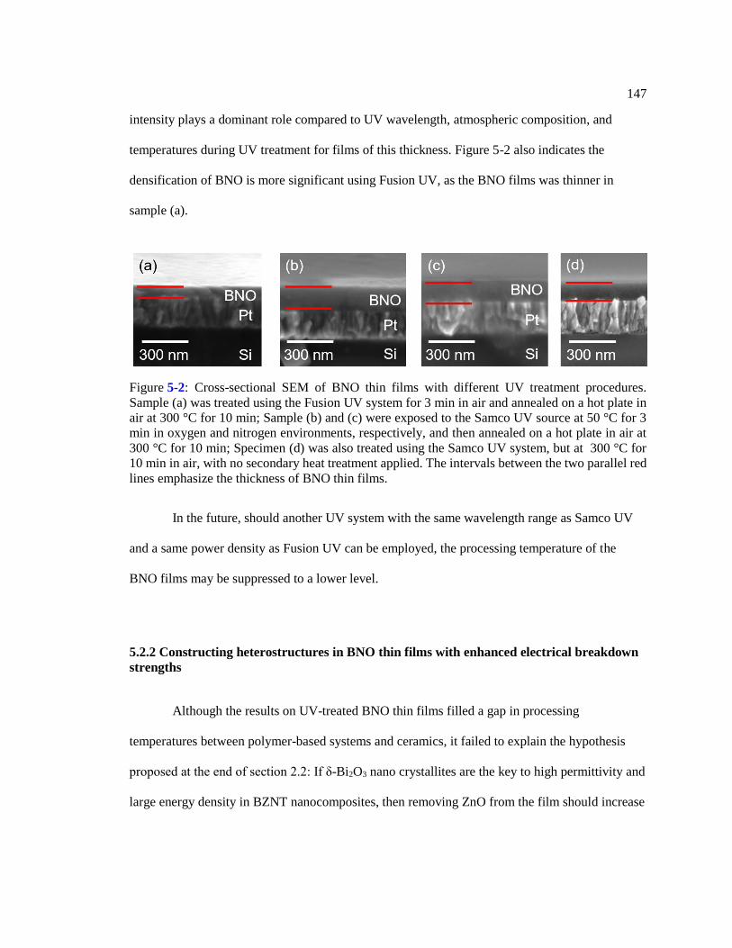
147
intensity plays a dominant role compared to UV wavelength, atmospheric composition, and
temperatures during UV treatment for films of this thickness. Figure 5-2 also indicates the
densification of BNO is more significant using Fusion UV, as the BNO films was thinner in
sample (a).
In the future, should another UV system with the same wavelength range as Samco UV
and a same power density as Fusion UV can be employed, the processing temperature of the
BNO films may be suppressed to a lower level.
5.2.2 Constructing heterostructures in BNO thin films with enhanced electrical breakdown
strengths
Although the results on UV-treated BNO thin films filled a gap in processing
temperatures between polymer-based systems and ceramics, it failed to explain the hypothesis
proposed at the end of section 2.2: If δ-Bi2O3 nano crystallites are the key to high permittivity and
large energy density in BZNT nanocomposites, then removing ZnO from the film should increase
Figure 5-2: Cross-sectional SEM of BNO thin films with different UV treatment procedures.
Sample (a) was treated using the Fusion UV system for 3 min in air and annealed on a hot plate in
air at 300 °C for 10 min; Sample (b) and (c) were exposed to the Samco UV source at 50 °C for 3
min in oxygen and nitrogen environments, respectively, and then annealed on a hot plate in air at
300 °C for 10 min; Specimen (d) was also treated using the Samco UV system, but at 300 °C for
10 min in air, with no secondary heat treatment applied. The intervals between the two parallel red
lines emphasize the thickness of BNO thin films.
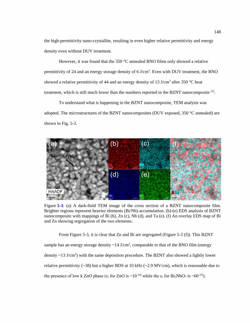
148
the high-permittivity nano-crystallite, resulting in even higher relative permittivity and energy
density even without DUV treatment.
However, it was found that the 350 °C annealed BNO films only showed a relative
permittivity of 24 and an energy storage density of 6 J/cm3. Even with DUV treatment, the BNO
showed a relative permittivity of 44 and an energy density of 13 J/cm3 after 350 °C heat
treatment, which is still much lower than the numbers reported in the BZNT nanocomposite [3].
To understand what is happening in the BZNT nanocomposite, TEM analysis was
adopted. The microstructures of the BZNT nanocomposites (DUV exposed, 350 °C annealed) are
shown in Fig. 5-3.
From Figure 5-3, it is clear that Zn and Bi are segregated (Figure 5-3 (f)). This BZNT
sample has an energy storage density ~14 J/cm3, comparable to that of the BNO film (energy
density ~13 J/cm3) with the same deposition procedure. The BZNT also showed a lightly lower
relative permittivity (~38) but a higher BDS at 10 kHz (~2.9 MV/cm), which is reasonable due to
the presence of low k ZnO phase (εr for ZnO is ~10 [4] while the εr for Bi3NbO7 is ~60 [5]).
Figure 5-3: (a) A dark-field TEM image of the cross section of a BZNT nanocomposite film.
Brighter regions represent heavier elements (Bi/Nb) accumulation. (b)-(e) EDS analysis of BZNT
nanocomposite with mappings of Bi (b), Zn (c), Nb (d), and Ta (e). (f) An overlay EDS map of Bi
and Zn showing segregation of the two elements.
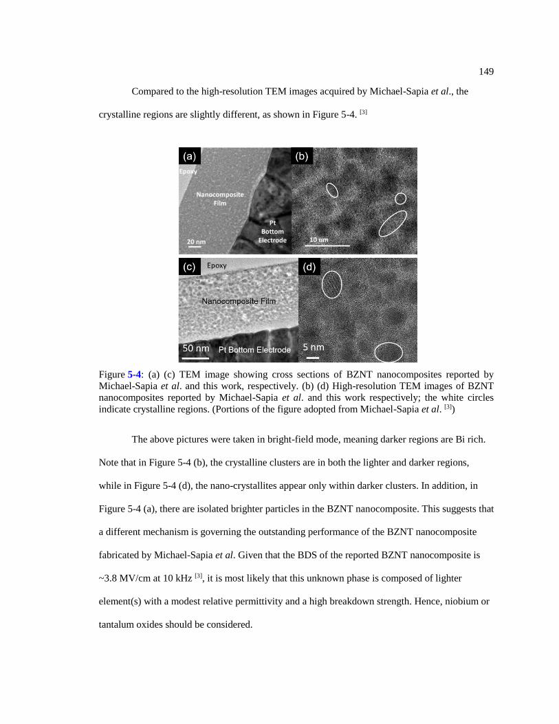
149
Compared to the high-resolution TEM images acquired by Michael-Sapia et al., the
crystalline regions are slightly different, as shown in Figure 5-4. [3]
The above pictures were taken in bright-field mode, meaning darker regions are Bi rich.
Note that in Figure 5-4 (b), the crystalline clusters are in both the lighter and darker regions,
while in Figure 5-4 (d), the nano-crystallites appear only within darker clusters. In addition, in
Figure 5-4 (a), there are isolated brighter particles in the BZNT nanocomposite. This suggests that
a different mechanism is governing the outstanding performance of the BZNT nanocomposite
fabricated by Michael-Sapia et al. Given that the BDS of the reported BZNT nanocomposite is
~3.8 MV/cm at 10 kHz [3], it is most likely that this unknown phase is composed of lighter
element(s) with a modest relative permittivity and a high breakdown strength. Hence, niobium or
tantalum oxides should be considered.
Figure 5-4: (a) (c) TEM image showing cross sections of BZNT nanocomposites reported by
Michael-Sapia et al. and this work, respectively. (b) (d) High-resolution TEM images of BZNT
nanocomposites reported by Michael-Sapia et al. and this work respectively; the white circles
indicate crystalline regions. (Portions of the figure adopted from Michael-Sapia et al. [3])
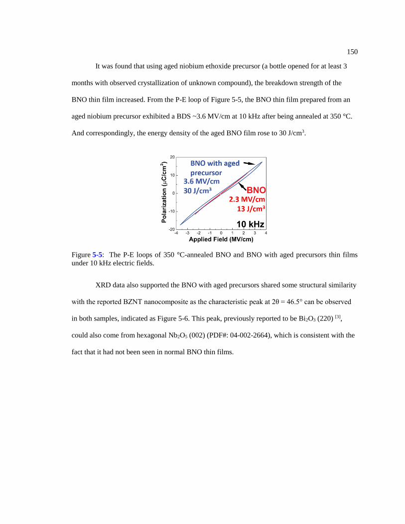
150
It was found that using aged niobium ethoxide precursor (a bottle opened for at least 3
months with observed crystallization of unknown compound), the breakdown strength of the
BNO thin film increased. From the P-E loop of Figure 5-5, the BNO thin film prepared from an
aged niobium precursor exhibited a BDS ~3.6 MV/cm at 10 kHz after being annealed at 350 °C.
And correspondingly, the energy density of the aged BNO film rose to 30 J/cm3.
XRD data also supported the BNO with aged precursors shared some structural similarity
with the reported BZNT nanocomposite as the characteristic peak at 2θ = 46.5° can be observed
in both samples, indicated as Figure 5-6. This peak, previously reported to be Bi2O3 (220) [3],
could also come from hexagonal Nb2O5 (002) (PDF#: 04-002-2664), which is consistent with the
fact that it had not been seen in normal BNO thin films.
Figure 5-5: The P-E loops of 350 °C-annealed BNO and BNO with aged precursors thin films
under 10 kHz electric fields.
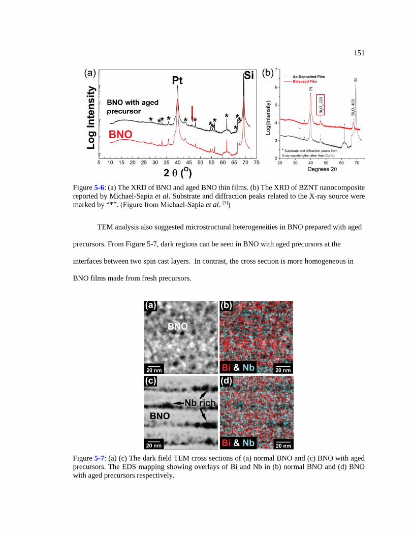
151
TEM analysis also suggested microstructural heterogeneities in BNO prepared with aged
precursors. From Figure 5-7, dark regions can be seen in BNO with aged precursors at the
interfaces between two spin cast layers. In contrast, the cross section is more homogeneous in
BNO films made from fresh precursors.
Figure 5-6: (a) The XRD of BNO and aged BNO thin films. (b) The XRD of BZNT nanocomposite
reported by Michael-Sapia et al. Substrate and diffraction peaks related to the X-ray source were
marked by “*”. (Figure from Michael-Sapia et al. [3])
Figure 5-7: (a) (c) The dark field TEM cross sections of (a) normal BNO and (c) BNO with aged
precursors. The EDS mapping showing overlays of Bi and Nb in (b) normal BNO and (d) BNO
with aged precursors respectively.
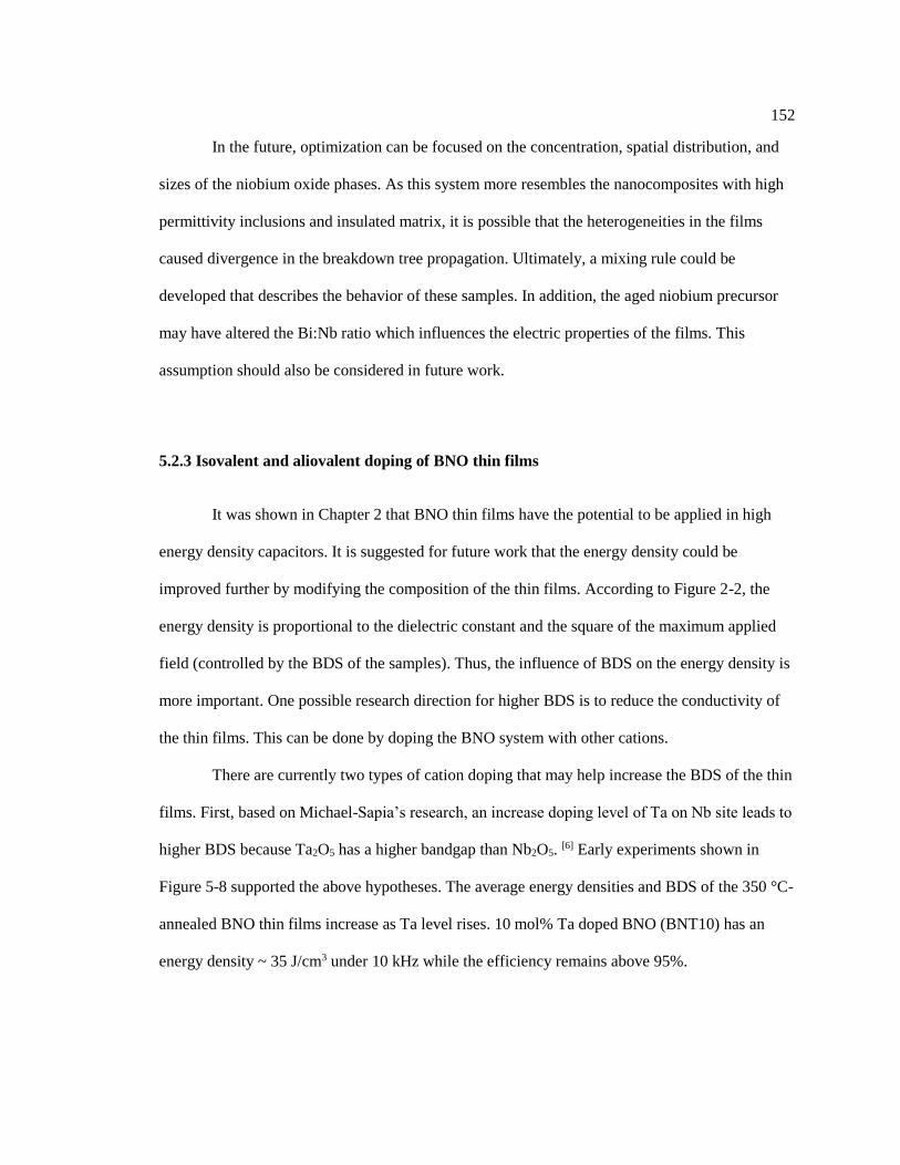
152
In the future, optimization can be focused on the concentration, spatial distribution, and
sizes of the niobium oxide phases. As this system more resembles the nanocomposites with high
permittivity inclusions and insulated matrix, it is possible that the heterogeneities in the films
caused divergence in the breakdown tree propagation. Ultimately, a mixing rule could be
developed that describes the behavior of these samples. In addition, the aged niobium precursor
may have altered the Bi:Nb ratio which influences the electric properties of the films. This
assumption should also be considered in future work.
5.2.3 Isovalent and aliovalent doping of BNO thin films
It was shown in Chapter 2 that BNO thin films have the potential to be applied in high
energy density capacitors. It is suggested for future work that the energy density could be
improved further by modifying the composition of the thin films. According to Figure 2-2, the
energy density is proportional to the dielectric constant and the square of the maximum applied
field (controlled by the BDS of the samples). Thus, the influence of BDS on the energy density is
more important. One possible research direction for higher BDS is to reduce the conductivity of
the thin films. This can be done by doping the BNO system with other cations.
There are currently two types of cation doping that may help increase the BDS of the thin
films. First, based on Michael-Sapia’s research, an increase doping level of Ta on Nb site leads to
higher BDS because Ta2O5 has a higher bandgap than Nb2O5. [6] Early experiments shown in
Figure 5-8 supported the above hypotheses. The average energy densities and BDS of the 350 °C-
annealed BNO thin films increase as Ta level rises. 10 mol% Ta doped BNO (BNT10) has an
energy density ~ 35 J/cm3 under 10 kHz while the efficiency remains above 95%.
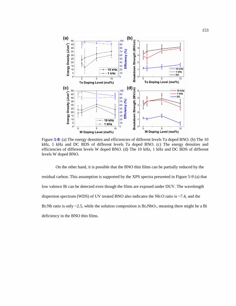
153
On the other hand, it is possible that the BNO thin films can be partially reduced by the
residual carbon. This assumption is supported by the XPS spectra presented in Figure 5-9 (a) that
low valence Bi can be detected even though the films are exposed under DUV. The wavelength
dispersion spectrum (WDS) of UV treated BNO also indicates the Nb:O ratio is ~7.4, and the
Bi:Nb ratio is only ~2.5, while the solution composition is Bi3NbO7, meaning there might be a Bi
deficiency in the BNO thin films.
Figure 5-8: (a) The energy densities and efficiencies of different levels Ta doped BNO. (b) The 10
kHz, 1 kHz and DC BDS of different levels Ta doped BNO. (c) The energy densities and
efficiencies of different levels W doped BNO. (d) The 10 kHz, 1 kHz and DC BDS of different
levels W doped BNO.
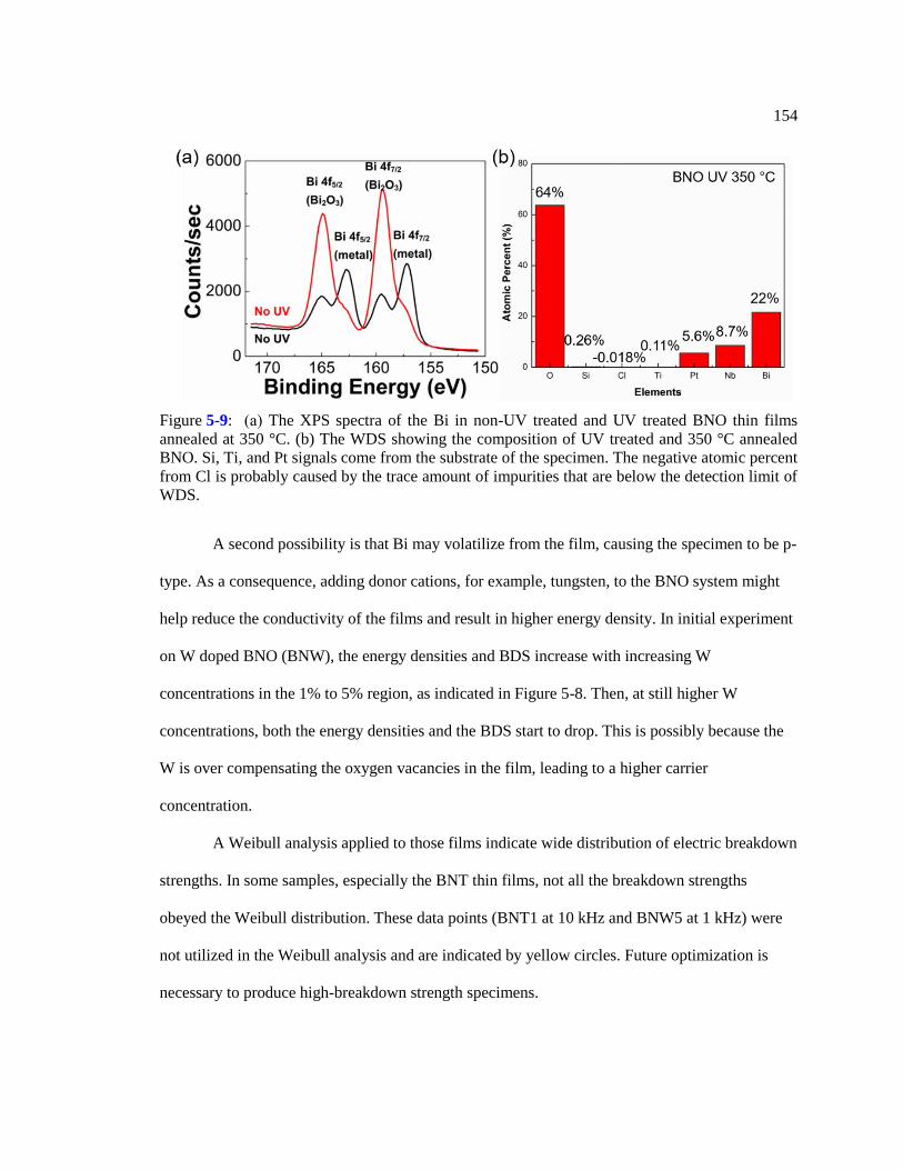
154
A second possibility is that Bi may volatilize from the film, causing the specimen to be p-
type. As a consequence, adding donor cations, for example, tungsten, to the BNO system might
help reduce the conductivity of the films and result in higher energy density. In initial experiment
on W doped BNO (BNW), the energy densities and BDS increase with increasing W
concentrations in the 1% to 5% region, as indicated in Figure 5-8. Then, at still higher W
concentrations, both the energy densities and the BDS start to drop. This is possibly because the
W is over compensating the oxygen vacancies in the film, leading to a higher carrier
concentration.
A Weibull analysis applied to those films indicate wide distribution of electric breakdown
strengths. In some samples, especially the BNT thin films, not all the breakdown strengths
obeyed the Weibull distribution. These data points (BNT1 at 10 kHz and BNW5 at 1 kHz) were
not utilized in the Weibull analysis and are indicated by yellow circles. Future optimization is
necessary to produce high-breakdown strength specimens.
Figure 5-9: (a) The XPS spectra of the Bi in non-UV treated and UV treated BNO thin films
annealed at 350 °C. (b) The WDS showing the composition of UV treated and 350 °C annealed
BNO. Si, Ti, and Pt signals come from the substrate of the specimen. The negative atomic percent
from Cl is probably caused by the trace amount of impurities that are below the detection limit of
WDS.
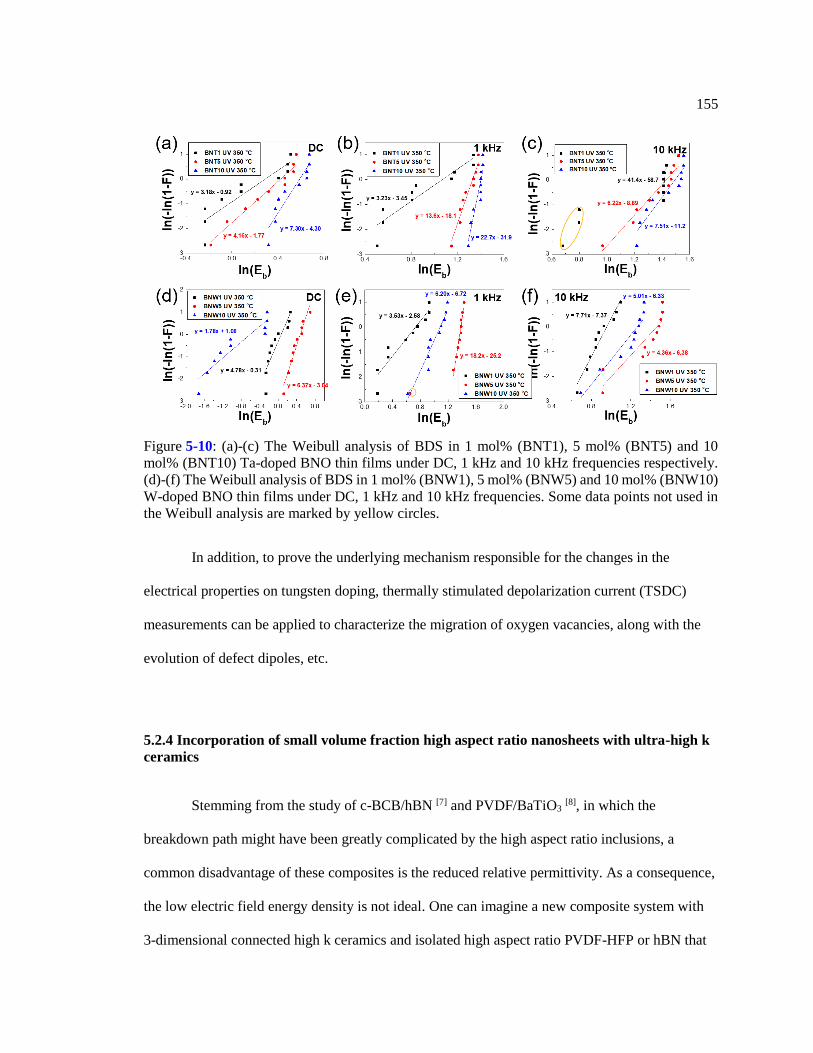
155
In addition, to prove the underlying mechanism responsible for the changes in the
electrical properties on tungsten doping, thermally stimulated depolarization current (TSDC)
measurements can be applied to characterize the migration of oxygen vacancies, along with the
evolution of defect dipoles, etc.
5.2.4 Incorporation of small volume fraction high aspect ratio nanosheets with ultra-high k
ceramics
Stemming from the study of c-BCB/hBN [7] and PVDF/BaTiO3 [8], in which the
breakdown path might have been greatly complicated by the high aspect ratio inclusions, a
common disadvantage of these composites is the reduced relative permittivity. As a consequence,
the low electric field energy density is not ideal. One can imagine a new composite system with
3-dimensional connected high k ceramics and isolated high aspect ratio PVDF-HFP or hBN that
Figure 5-10: (a)-(c) The Weibull analysis of BDS in 1 mol% (BNT1), 5 mol% (BNT5) and 10
mol% (BNT10) Ta-doped BNO thin films under DC, 1 kHz and 10 kHz frequencies respectively.
(d)-(f) The Weibull analysis of BDS in 1 mol% (BNW1), 5 mol% (BNW5) and 10 mol% (BNW10)
W-doped BNO thin films under DC, 1 kHz and 10 kHz frequencies. Some data points not used in
the Weibull analysis are marked by yellow circles.
156
are parallel, dispersed, and normal to the electric field direction. Because of the small volume
fraction of low permittivity inclusions, this nanocomposite should preserve a high relative
permittivity from the ceramic matrix while presenting improved BDS due to the existence of
insulating phases. Such system may help improving the energy storage performances of ceramics
such as PbMg1/3Nb2/3O3-based [9], BaTiO3-based [10], and NaNbO3-based [11] ceramics. These
ceramics all displays high relative permittivities, but the breakdown strength is low.
One challenge of fabricating high ceramic volume fraction composites is the sintering of
ceramic powders. Because conventionally, ceramic powders need to be densified at ~50-75% of
their melting temperatures that the fabrication temperatures of bulk ceramic capacitors are
generally over 1000 °C, nanosheet inclusions are subject to decomposition or melting during
sintering. The cold sintering process may offer a solution to densify these ceramics below 300 °C.
A similar system was successfully demonstrated by cold sintering ZnO/PTFE. [12]
5.2.5 CSP of functional PZT without post-annealing using NaOH/KOH eutectic flux
The cold sintering process, whether via transient liquid phases or viscous flow, is a
technique used to sinter ceramic materials at temperatures significantly lower than those
processed in furnaces. However, there are a number of materials that need to be post-annealed
after CSP to achieve the full range of functional properties. These include perovskites (PZT,
BTO), fluorites (YSZ), and spinels (Fe3O4). These ceramics are difficult to dissolve in a water-
based system and are hard enough to resist plastic deformation during CSP.
One alternative approach to densify cold sintered ceramics is to utilize molten salts.
Molten salts are commonly seen in the synthesis of oxides with limited solubility in water, such
as Al2O3 [13] and BaTiO3
[14]. Recently, carbides and nitrates sintering processes [15] have also been
proved compatible with molten salts. Regarding the selection of salt systems, Liu et al.
157
recommended a qualitative “hard-soft acid-base (HSAB)” theory [16] in which the cations and
anions are categorized into hard/soft acid/base. “Hard” represents cations (acids) or anions
(bases) with small ionic radii, high charges, low (for acids) or high (for bases) electronegativities,
and weak polarizabilities; “Soft” refers to cations (acids) or anions (bases) that are large-sized,
low-charged, with intermediate values of electronegativity, and strongly polarized.[17,18] “Hard”
acids tend to react or form solvents with “hard” bases, and vice versa. This theory might
alternatively be explained through the “valence-matching principle” where the Lewis basicity of
anions and the Lewis acidity of cations must be matched to form a stable structure. [19] For PZT,
the “hard” nature of Zr4+ and Ti4+ suggest good solubilities with alkali metal fluorides and
chlorides, while Pb2+ is an intermediate cation between “hard” and “soft”. However, the melting
points of most fluorides and chlorides are still too high to be incorporated in the CSP. For
example, LiF only drops the sintering temperature of PZT to ~ 900-950 °C. Similarly, the eutectic
composition, NaCl/KCl still has a melting point of 658 °C [16]
Consequently, oxosalts such as NaOH and KOH are of interest. At the eutectic
composition (NaOH/KOH = 51 mol%/49 mol%), NaOH/KOH has a melting point of 170 °C, as
indicated by the phase diagram (Figure 5-11).
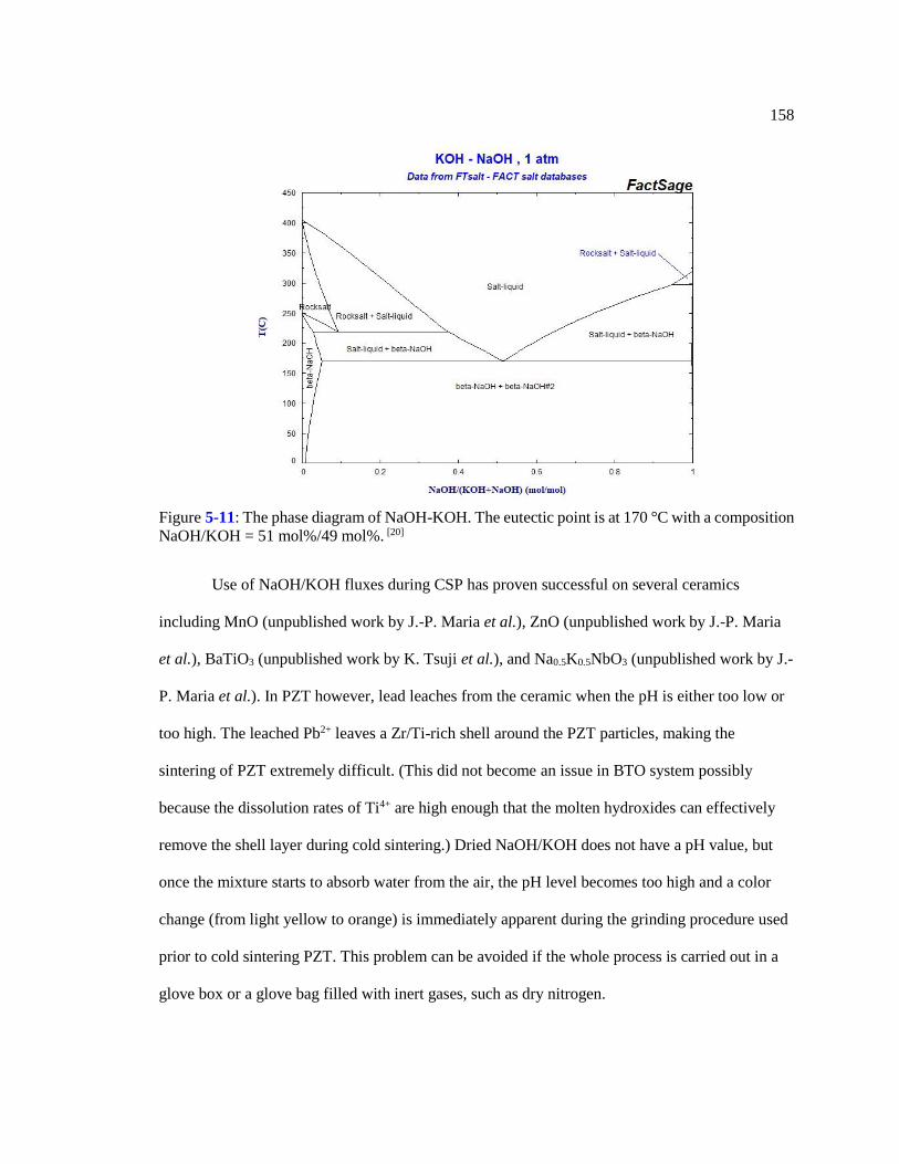
158
Use of NaOH/KOH fluxes during CSP has proven successful on several ceramics
including MnO (unpublished work by J.-P. Maria et al.), ZnO (unpublished work by J.-P. Maria
et al.), BaTiO3 (unpublished work by K. Tsuji et al.), and Na0.5K0.5NbO3 (unpublished work by J.-
P. Maria et al.). In PZT however, lead leaches from the ceramic when the pH is either too low or
too high. The leached Pb2+ leaves a Zr/Ti-rich shell around the PZT particles, making the
sintering of PZT extremely difficult. (This did not become an issue in BTO system possibly
because the dissolution rates of Ti4+ are high enough that the molten hydroxides can effectively
remove the shell layer during cold sintering.) Dried NaOH/KOH does not have a pH value, but
once the mixture starts to absorb water from the air, the pH level becomes too high and a color
change (from light yellow to orange) is immediately apparent during the grinding procedure used
prior to cold sintering PZT. This problem can be avoided if the whole process is carried out in a
glove box or a glove bag filled with inert gases, such as dry nitrogen.
Figure 5-11: The phase diagram of NaOH-KOH. The eutectic point is at 170 °C with a composition
NaOH/KOH = 51 mol%/49 mol%. [20]
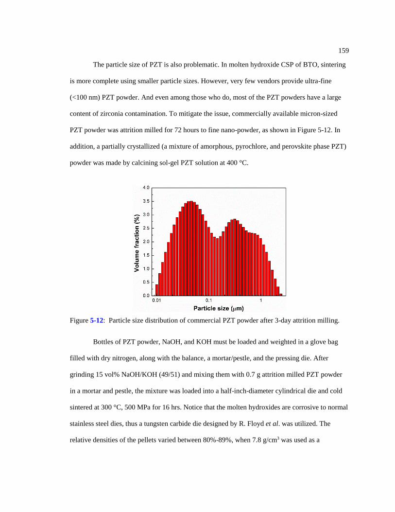
159
The particle size of PZT is also problematic. In molten hydroxide CSP of BTO, sintering
is more complete using smaller particle sizes. However, very few vendors provide ultra-fine
(<100 nm) PZT powder. And even among those who do, most of the PZT powders have a large
content of zirconia contamination. To mitigate the issue, commercially available micron-sized
PZT powder was attrition milled for 72 hours to fine nano-powder, as shown in Figure 5-12. In
addition, a partially crystallized (a mixture of amorphous, pyrochlore, and perovskite phase PZT)
powder was made by calcining sol-gel PZT solution at 400 °C.
Bottles of PZT powder, NaOH, and KOH must be loaded and weighted in a glove bag
filled with dry nitrogen, along with the balance, a mortar/pestle, and the pressing die. After
grinding 15 vol% NaOH/KOH (49/51) and mixing them with 0.7 g attrition milled PZT powder
in a mortar and pestle, the mixture was loaded into a half-inch-diameter cylindrical die and cold
sintered at 300 °C, 500 MPa for 16 hrs. Notice that the molten hydroxides are corrosive to normal
stainless steel dies, thus a tungsten carbide die designed by R. Floyd et al. was utilized. The
relative densities of the pellets varied between 80%-89%, when 7.8 g/cm3 was used as a
Figure 5-12: Particle size distribution of commercial PZT powder after 3-day attrition milling.
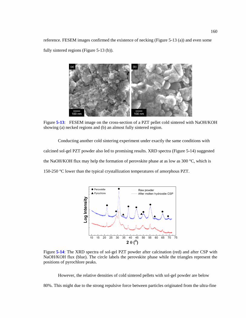
160
reference. FESEM images confirmed the existence of necking (Figure 5-13 (a)) and even some
fully sintered regions (Figure 5-13 (b)).
Conducting another cold sintering experiment under exactly the same conditions with
calcined sol-gel PZT powder also led to promising results. XRD spectra (Figure 5-14) suggested
the NaOH/KOH flux may help the formation of perovskite phase at as low as 300 °C, which is
150-250 °C lower than the typical crystallization temperatures of amorphous PZT.
However, the relative densities of cold sintered pellets with sol-gel powder are below
80%. This might due to the strong repulsive force between particles originated from the ultra-fine
Figure 5-13: FESEM image on the cross-section of a PZT pellet cold sintered with NaOH/KOH
showing (a) necked regions and (b) an almost fully sintered region.
Figure 5-14: The XRD spectra of sol-gel PZT powder after calcination (red) and after CSP with
NaOH/KOH flux (blue). The circle labels the perovskite phase while the triangles represent the
positions of pyrochlore peaks.
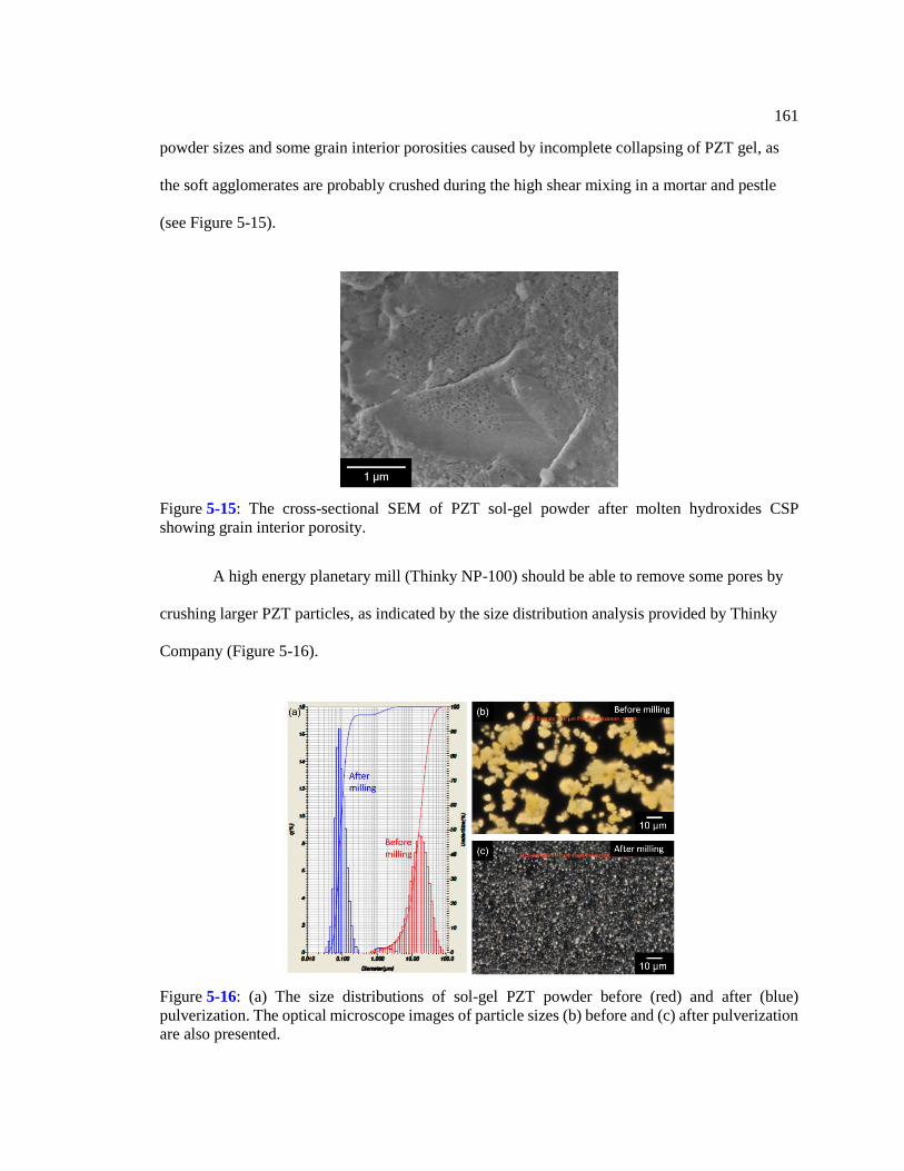
161
powder sizes and some grain interior porosities caused by incomplete collapsing of PZT gel, as
the soft agglomerates are probably crushed during the high shear mixing in a mortar and pestle
(see Figure 5-15).
A high energy planetary mill (Thinky NP-100) should be able to remove some pores by
crushing larger PZT particles, as indicated by the size distribution analysis provided by Thinky
Company (Figure 5-16).
Figure 5-15: The cross-sectional SEM of PZT sol-gel powder after molten hydroxides CSP
showing grain interior porosity.
Figure 5-16: (a) The size distributions of sol-gel PZT powder before (red) and after (blue)
pulverization. The optical microscope images of particle sizes (b) before and (c) after pulverization
are also presented.
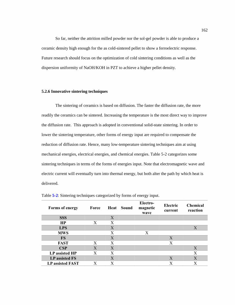
162
So far, neither the attrition milled powder nor the sol-gel powder is able to produce a
ceramic density high enough for the as cold-sintered pellet to show a ferroelectric response.
Future research should focus on the optimization of cold sintering conditions as well as the
dispersion uniformity of NaOH/KOH in PZT to achieve a higher pellet density.
5.2.6 Innovative sintering techniques
The sintering of ceramics is based on diffusion. The faster the diffusion rate, the more
readily the ceramics can be sintered. Increasing the temperature is the most direct way to improve
the diffusion rate. This approach is adopted in conventional solid-state sintering. In order to
lower the sintering temperature, other forms of energy input are required to compensate the
reduction of diffusion rate. Hence, many low-temperature sintering techniques aim at using
mechanical energies, electrical energies, and chemical energies. Table 5-2 categorizes some
sintering techniques in terms of the forms of energies input. Note that electromagnetic wave and
electric current will eventually turn into thermal energy, but both alter the path by which heat is
delivered.
Table 5-2: Sintering techniques categorized by forms of energy input.
Forms of energy Force Heat Sound
Electro-
magnetic
wave
Electric
current
Chemical
reaction
SSS X
HP X X
LPS X X
MWS X X
FS X X
FAST X X X
CSP X X X
LP assisted HP X X X
LP assisted FS X X X
LP assisted FAST X X X X
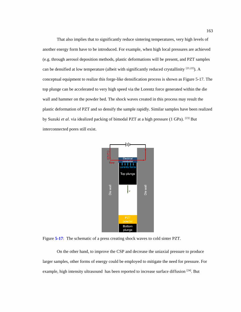
163
That also implies that to significantly reduce sintering temperatures, very high levels of
another energy form have to be introduced. For example, when high local pressures are achieved
(e.g. through aerosol deposition methods, plastic deformations will be present, and PZT samples
can be densified at low temperature (albeit with significantly reduced crystallinity [21,22]). A
conceptual equipment to realize this forge-like densification process is shown as Figure 5-17. The
top plunge can be accelerated to very high speed via the Lorentz force generated within the die
wall and hammer on the powder bed. The shock waves created in this process may result the
plastic deformation of PZT and so densify the sample rapidly. Similar samples have been realized
by Suzuki et al. via idealized packing of bimodal PZT at a high pressure (1 GPa). [23] But
interconnected pores still exist.
On the other hand, to improve the CSP and decrease the uniaxial pressure to produce
larger samples, other forms of energy could be employed to mitigate the need for pressure. For
example, high intensity ultrasound has been reported to increase surface diffusion [24]. But
Figure 5-17: The schematic of a press creating shock waves to cold sinter PZT.
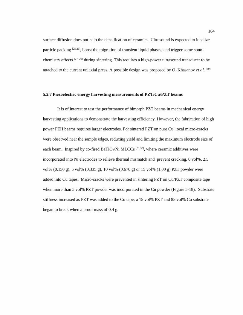
164
surface diffusion does not help the densification of ceramics. Ultrasound is expected to idealize
particle packing [25,26], boost the migration of transient liquid phases, and trigger some sono-
chemistry effects [27–29] during sintering. This requires a high-power ultrasound transducer to be
attached to the current uniaxial press. A possible design was proposed by O. Khasanov et al. [30]
5.2.7 Piezoelectric energy harvesting measurements of PZT/Cu/PZT beams
It is of interest to test the performance of bimorph PZT beams in mechanical energy
harvesting applications to demonstrate the harvesting efficiency. However, the fabrication of high
power PEH beams requires larger electrodes. For sintered PZT on pure Cu, local micro-cracks
were observed near the sample edges, reducing yield and limiting the maximum electrode size of
each beam. Inspired by co-fired BaTiO3/Ni MLCCs [31,32], where ceramic additives were
incorporated into Ni electrodes to relieve thermal mismatch and prevent cracking, 0 vol%, 2.5
vol% (0.150 g), 5 vol% (0.335 g), 10 vol% (0.670 g) or 15 vol% (1.00 g) PZT powder were
added into Cu tapes. Micro-cracks were prevented in sintering PZT on Cu/PZT composite tape
when more than 5 vol% PZT powder was incorporated in the Cu powder (Figure 5-18). Substrate
stiffness increased as PZT was added to the Cu tape; a 15 vol% PZT and 85 vol% Cu substrate
began to break when a proof mass of 0.4 g.
165
5.2.8 Cold sintering textured PZT thick films on metal substrates for high FoM PEH
Currently, all cold sintered materials are randomly oriented. Randomly oriented PZT has
reduced e31,f and large relative permittivity, giving low FoM for energy harvesting applications.
Textured PZT fabricated by co-casting PZT powder and high aspect ratio BaTiO3 as a seed for
templated grain growth promises higher FoM but the grain growth rate is quite limited in PZT
during sintering. [33] This produces a lower Lotgering factor in PZT compared to other lead-based
Figure 5-18: The top surface SEM of 800 °C post-sintered PZT on (a) pure Cu tape, (b) Cu/PZT
with 2.5 vol% PZT inclusion, (c) Cu/PZT with 5 vol% PZT inclusion, (d) Cu/PZT with 10 vol%
PZT inclusion, and (e) Cu/PZT with 15 vol% PZT inclusion.
166
relaxors [34]. With CSP [35], grain growth in PZT pellets has been observed at 700 °C, providing a
potential solution. However, studies on textured ceramic CSP rely on tape cold sintering, which
needs additional development. For instance, Bordia et al. found that a high sample aspect ratio
benefited the in-plane directional “necking” and reduced the driving force for out-of-plane
directional pore shrinkage.[36] Sudre et al [37] indicated the removal of porosity in ceramics with
high aspect ratio inclusions is influenced by a non-uniform transformation strain. Additionally,
large uniaxial pressure may crush BaTiO3 and disturb the alignment of the templates during CSP.
[38] If the cold sintering process can be carried out at 300 °C, the required pressure of the CSP to
reach the same density may decrease.
5.2.9 A design of multi-layered piezo MEMS structure for high power PEH
A stack of multi-layered PZT films, instead of one layer of piezoelectric ceramic on each
side of the substrate, should improve the open circuit voltage of PEHs. However, multi-layer
stacks have stress/strain distribution issues. Zhu et al. found the efficiency of multi-layered PEH
drops as the number of layers increase; it is not worthwhile to stack more than 2 layers due to
decreased power output. [39] This is likely due to the existence of strain gradients along thickness,
as shown in Figure 5-19. A layer of material(s) placed between two stacks to pre-bias the
piezoelectrics with compressive strain or simply a layer of elastomers to relieve the strain would
allow further stacking before cracking occurs.
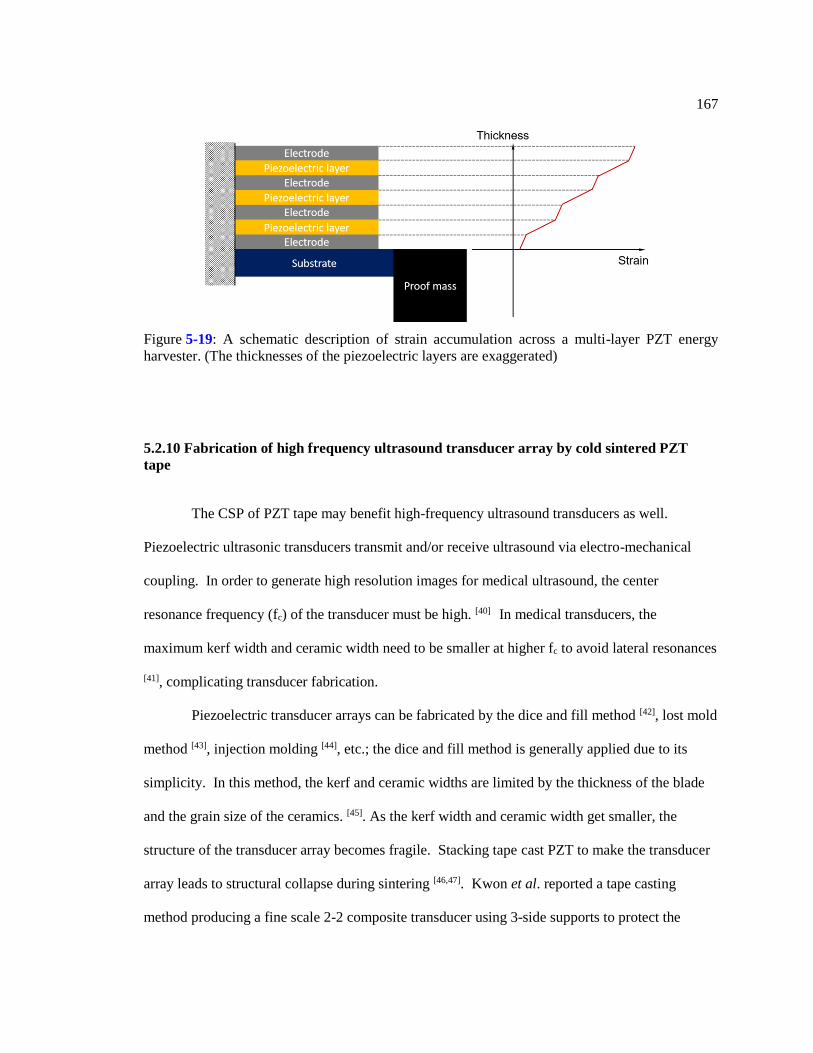
167
5.2.10 Fabrication of high frequency ultrasound transducer array by cold sintered PZT
tape
The CSP of PZT tape may benefit high-frequency ultrasound transducers as well.
Piezoelectric ultrasonic transducers transmit and/or receive ultrasound via electro-mechanical
coupling. In order to generate high resolution images for medical ultrasound, the center
resonance frequency (fc) of the transducer must be high. [40] In medical transducers, the
maximum kerf width and ceramic width need to be smaller at higher fc to avoid lateral resonances
[41], complicating transducer fabrication.
Piezoelectric transducer arrays can be fabricated by the dice and fill method [42], lost mold
method [43], injection molding [44], etc.; the dice and fill method is generally applied due to its
simplicity. In this method, the kerf and ceramic widths are limited by the thickness of the blade
and the grain size of the ceramics. [45]. As the kerf width and ceramic width get smaller, the
structure of the transducer array becomes fragile. Stacking tape cast PZT to make the transducer
array leads to structural collapse during sintering [46,47]. Kwon et al. reported a tape casting
method producing a fine scale 2-2 composite transducer using 3-side supports to protect the
Figure 5-19: A schematic description of strain accumulation across a multi-layer PZT energy
harvester. (The thicknesses of the piezoelectric layers are exaggerated)
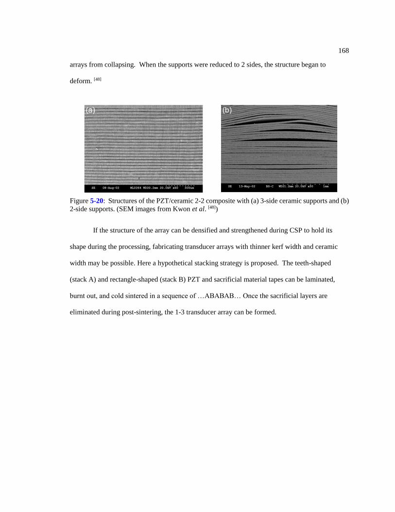
168
arrays from collapsing. When the supports were reduced to 2 sides, the structure began to
deform. [48]
If the structure of the array can be densified and strengthened during CSP to hold its
shape during the processing, fabricating transducer arrays with thinner kerf width and ceramic
width may be possible. Here a hypothetical stacking strategy is proposed. The teeth-shaped
(stack A) and rectangle-shaped (stack B) PZT and sacrificial material tapes can be laminated,
burnt out, and cold sintered in a sequence of …ABABAB… Once the sacrificial layers are
eliminated during post-sintering, the 1-3 transducer array can be formed.
Figure 5-20: Structures of the PZT/ceramic 2-2 composite with (a) 3-side ceramic supports and (b)
2-side supports. (SEM images from Kwon et al. [48])
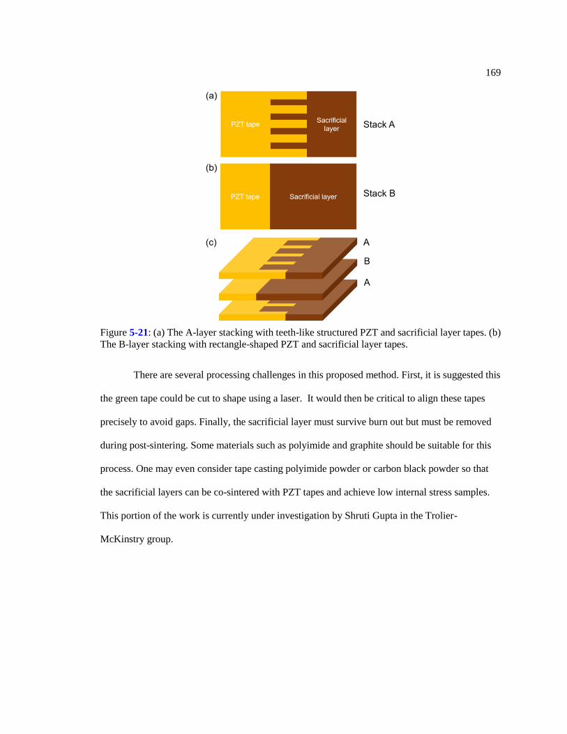
169
There are several processing challenges in this proposed method. First, it is suggested this
the green tape could be cut to shape using a laser. It would then be critical to align these tapes
precisely to avoid gaps. Finally, the sacrificial layer must survive burn out but must be removed
during post-sintering. Some materials such as polyimide and graphite should be suitable for this
process. One may even consider tape casting polyimide powder or carbon black powder so that
the sacrificial layers can be co-sintered with PZT tapes and achieve low internal stress samples.
This portion of the work is currently under investigation by Shruti Gupta in the Trolier-
McKinstry group.
Figure 5-21: (a) The A-layer stacking with teeth-like structured PZT and sacrificial layer tapes. (b)
The B-layer stacking with rectangle-shaped PZT and sacrificial layer tapes.
170
References
[1] Kolah, A. K.; Asthana, N. S.; Vu, D. T.; Lira, C. T.; Miller, D. J. Reaction Kinetics of the
Catalytic Esterification of Citric Acid with Ethanol. Ind. Eng. Chem. Res. 2007, 46 (10), 3180–
3187.
[2] Xu, H.; Zhu, T.; Yu, R. P. Study on the Absorption and Fluorescence Spectra of Ethylene
Glycol and Glycerol. Guang Pu Xue Yu Guang Pu Fen Xi/Spectroscopy Spectr. Anal. 2007, 27
(7), 1381–1384.
[3] Michael-Sapia, E. K.; Li, H. U.; Jackson, T. N.; Trolier-McKinstry, S. Nanocomposite
Bismuth Zinc Niobate Tantalate for Flexible Energy Storage Applications. J. Appl. Phys. 2015,
118 (23), 234102.
[4] Langton, N. H.; Matthews, D. The Dielectric Constant of Zinc Oxide over a Range of
Frequencies. Br. J. Appl. Phys. 1958, 9 (11), 453–456.
[5] Valant, M.; Suvorov, D. Dielectric Characteristics of Bismuth Oxide Solid Solutions with a
Fluorite-Like Crystal Structure. J. Am. Ceram. Soc. 2004, 87 (6), 1056–1061.
[6] Michael, E. K.; Trolier-McKinstry, S. Bismuth Pyrochlore-Based Thin Films for Dielectric
Energy Storage, Pennsylvania State University, 2015.
[7] Li, Q.; Chen, L.; Gadinski, M. R.; Zhang, S.; Zhang, G.; Li, H.; Haque, A.; Chen, L.-Q.;
Jackson, T.; Wang, Q. Flexible High-Temperature Dielectric Materials from Polymer
Nanocomposites. Nature 2015, 523 (7562), 576–579.
[8] Shen, Z. H.; Wang, J. J.; Lin, Y.; Nan, C. W.; Chen, L. Q.; Shen, Y. High-Throughput Phase-
Field Design of High-Energy-Density Polymer Nanocomposites. Adv. Mater. 2018, 30 (2), 1–6.
[9] Bridger, K.; Sutherland, A.; Fiore, E.; Bailey, A.; Christodoulou, J.; Winzer, S. Lead
Magnesium Niobate Dielectrics for High-Field Applications. In Proceedings of the IEEE 35th
International Power Sources Symposium; IEEE, 1992; pp 387–390.
171
[10] Yang, H.; Yan, F.; Lin, Y.; Wang, T.; Wang, F.; Wang, Y.; Guo, L.; Tai, W.; Wei, H. Lead-
Free BaTiO3-Bi0.5Na0.5TiO3-Na0.73Bi0.09NbO3 Relaxor Ferroelectric Ceramics for High Energy
Storage. J. Eur. Ceram. Soc. 2017, 37 (10), 3303–3311.
[11] Zhou, M.; Liang, R.; Zhou, Z.; Dong, X. Achieving Ultrahigh Energy Storage Density and
Energy Efficiency Simultaneously in Sodium Niobate-Based Lead-Free Dielectric Capacitors via
Microstructure Modulation. Inorg. Chem. Front. 2019, 6 (8), 2148–2157.
[12] Zhao, X.; Guo, J.; Wang, K.; Herisson De Beauvoir, T.; Li, B.; Randall, C. A. Introducing a
ZnO–PTFE (Polymer) Nanocomposite Varistor via the Cold Sintering Process. Adv. Eng. Mater.
2018, 20 (7), 1–8.
[13] Du, Y.; Inman, D. Precipitation of Finely Divided A12O3 Powders by a Molten Salt Method.
J. Mater. Chem. 1996, 6 (7), 1239–1240.
[14] Liu, H.; Hu, C.; Wang, Z. L. Composite-Hydroxide-Mediated Approach for the Synthesis of
Nanostructures of Complex Functional-Oxides. Nano Lett. 2006, 6 (7), 1535–1540.
[15] Dash, A.; Vaßen, R.; Guillon, O.; Gonzalez-Julian, J. Molten Salt Shielded Synthesis of
Oxidation Prone Materials in Air. Nat. Mater. 2019, 18 (5), 465–470.
[16] Liu, X.; Fechler, N.; Antonietti, M. Salt Melt Synthesis of Ceramics, Semiconductors and
Carbon Nanostructures. Chem. Soc. Rev. 2013, 42 (21), 8237–8265.
[17] Pearson, R. G. Hard and Soft Acids and Bases, HSAB, Part I: Fundamental Principles. J.
Chem. Educ. 1968, 45 (9), 581–587.
[18] Pearson, R. G. Hard and Soft Acids and Bases, HSAB, Part II: Underlying Theories. J.
Chem. Educ. 1968, 45 (10), 643–648.
[19] Hawthorne, F. C. Toward Theoretical Mineralogy: A Bond-Topological Approach. Am.
Mineral. 2015, 100 (4), 696–713.
[20] Centre for Research in Computational Thermochemistry. KOH-NaOH phase diagram
http://www.crct.polymtl.ca/fact/phase_diagram.php?file=KOH-NaOH.jpg&dir=FTsalt%0A.
172
[21] Akedo, J. Room Temperature Impact Consolidation (RTIC) of Fine Ceramic Powder by
Aerosol Deposition Method and Applications to Microdevices. J. Therm. Spray Technol. 2008,
17 (2), 181–198.
[22] Akedo, J.; Lebedev, M. Piezoelectric Properties and Poling Effect of Pb(Zr, Ti)O3 Thick
Films Prepared for Microactuators by Aerosol Deposition. Appl. Phys. Lett. 2000, 77 (11), 1710–
1712.
[23] Suzuki, M.; Ushijima, H.; Tsuchiya, T.; Akedo, J. Polarization Properties of Aggregate PZT
Films Produced at Room Temperature. In Proceedings of the 19th US-Japan Seminar on
Dielectric & Piezoelectric Ceramics; Kato, K., Brennecka, G., Eds.; Tsukuba, Japan, 2019; pp
147–148.
[24] Shugaev, M. V.; Manzo, A. J.; Wu, C.; Zaitsev, V. Y.; Helvajian, H.; Zhigilei, L. V. Strong
Enhancement of Surface Diffusion by Nonlinear Surface Acoustic Waves. Phys. Rev. B -
Condens. Matter Mater. Phys. 2015, 91 (23), 1–11.
[25] Cha, H. R. Densification of the Nanopowder by Using Ultrasonic Vibration Compaction.
Rev. Adv. Mater. Sci. 2011, 28 (1), 90–93.
[26] Karban, O.; Kanunnikova, O.; Khazanov, E.; Salamatov, E.; Khasanov, O.; Taranov, A.
Structure and Composition of Ba-W-Ti-O Ceramics Interface Regions Formed at Ultrasonic
Vibration. ISRN Nanomater. 2012, 2012, 1–7.
[27] Xu, M.; Lu, Y. N.; Liu, Y. F.; Shi, S. Z.; Qian, T. S.; Lu, D. Y. Sonochemical Synthesis of
Monosized Spherical BaTiO3 Particles. Powder Technol. 2006, 161 (3), 185–189.
[28] Wirunchit, S.; Charoonsuk, T.; Vittayakorn, N. Facile Sonochemical Synthesis of Near
Spherical Barium Zirconate Titanate (BaZr1-yTiyO3; BZT); Perovskite Stability and Formation
Mechanism. RSC Adv. 2015, 5 (48), 38061–38074.
173
[29] Xu, Z. J.; Chu, R. Q.; Li, G. R.; Shao, X.; Yin, Q. R. Preparation of PZT Powders and
Ceramics via a Hybrid Method of Sol-Gel and Ultrasonic Atomization. Mater. Sci. Eng. B Solid-
State Mater. Adv. Technol. 2005, 117 (2), 113–118.
[30] Khasanov, O.; Dvilis, E.; Sokolov, V.; Pokholkov, Y. Mechanisms of Dry Powder Net-
Shaping Under Ultrasonic Vibration and By the Collector Method. In Proceedings of the 2nd
International Congress on Ceramics; Institute of Science and Technology for Ceramics-National
Research Council, 2008; pp 359–368.
[31] Sugimura, K.; Hirao, K. Effect of a BaTiO3 Nanoparticle Additive on the Quality of Thin-
Film Ni Electrodes in MLCC. J. Ceram. Soc. Japan 2009, 117 (1369), 1039–1043.
[32] Kang, J.-H.; Joo, D.; Cha, H.-M.; Jung, Y.-G.; Paik, U. Shrinkage Behavior and Interfacial
Diffusion in Ni-Based Internal Electrodes with BaTiO3 Additive. Ceram. Int. 2008, 34 (6), 1487–
1494.
[33] Muramatsu, H.; Kimura, T. Preparation of Bulk Pb(Zr, Ti)O3 with Crystallographic Texture
by Templated Grain Growth Method. J. Electroceramics 2004, 13 (1–3), 531–535.
[34] Chang, Y.; Watson, B.; Fanton, M.; Meyer, R. J.; Messing, G. L. Enhanced Texture
Evolution and Piezoelectric Properties in CuO-Doped Pb(In1/2Nb1/2)O3-Pb(Mg1/3Nb2/3)O3-PbTiO3
Grain-Oriented Ceramics. Appl. Phys. Lett. 2017, 111 (23), 232901.
[35] Wang, D.; Guo, H.; Morandi, C. S.; Randall, C. A.; Trolier-McKinstry, S. Cold Sintering
and Electrical Characterization of Lead Zirconate Titanate Piezoelectric Ceramics. APL Mater.
2018, 6 (1), 016101.
[36] Bordia, R. K.; Scherer, G. W. On Constrained Sintering—III. Rigid Inclusions. Acta Metall.
1988, 36 (9), 2411–2416.
[37] Sudre, O.; Bao, G.; Fan, B.; Lange, F. F.; Evans, A. G. Effect of Inclusions on Densification:
II, Numerical Model. J. Am. Ceram. Soc. 1992, 75 (3), 525–531.
174
[38] Uskokovic, D. P.; Palmour III, H.; Spriggs, R. M. Science of Sintering; Uskoković, D. P.,
Palmour, H., Spriggs, R. M., Eds.; Springer US: Boston, MA, 1989.
[39] Zhu, D.; Almusallam, A.; Beeby, S. P.; Tudor, J.; Harris, N. R. A Bimorph Multi-Layer
Piezoelectric Vibration Energy Harvester. In Proceedings of PowerMEMS; IOP Publishing, 2010;
pp 335–338.
[40] Zhou, Q.; Lau, S.; Wu, D.; Kirk Shung, K. Piezoelectric Films for High Frequency
Ultrasonic Transducers in Biomedical Applications. Prog. Mater. Sci. 2011, 56 (2), 139–174.
[41] Ritter, T. A.; Shrout, T. R.; Tutwiler, R.; Shung, K. K. A 30-MHz Piezo-Composite
Ultrasound Array for Medical Imaging Applications. IEEE Trans. Ultrason. Ferroelectr. Freq.
Control 2002, 49 (2), 217–230.
[42] Savakus, H. P.; Klicker, K. A.; Newnham, R. E. PZT-Epoxy Piezoelectric Transducers: A
Simplified Fabrication Procedure. Mater. Res. Bull. 1981, 16 (6), 677–680.
[43] Becker, E. W.; Ehrfeld, W.; Hagmann, P.; Maner, A.; Münchmeyer, D. Fabrication of
Microstructures with High Aspect Ratios and Great Structural Heights by Synchrotron Radiation
Lithography, Galvanoforming, and Plastic Moulding (LIGA Process). Microelectron. Eng. 1986,
4 (1), 35–56.
[44] Bowen, L. J.; French, K. W. Fabrication of Piezoelectric Ceramic/Polymer Composites by
Injection Molding. In ISAF ’92: Proceedings of the Eighth IEEE International Symposium on
Applications of Ferroelectrics; IEEE, 1992; pp 160–163.
[45] Janas, V. F.; Safari, A. Overview of Fine-Scale Piezoelectric Ceramic/Polymer Composite
Processing. J. Am. Ceram. Soc. 1995, 78 (11), 2945–2955.
[46] Hackenberger, W.; Ming-Jen Pan; Kuban, D.; Ritter, T.; Shrout, T. Novel Method for
Producing High Frequency 2-2 Composites from PZT Ceramic. In Proceedings of the 2000 IEEE
Ultrasonics Symposium. Proceedings. An International Symposium (Cat. No.00CH37121); IEEE,
2000; Vol. 2, pp 969–972.
175
[47] Zhang, Y.; Jiang, Y.; Lin, X.; Xie, R.; Zhou, K.; Button, T. W.; Zhang, D. Fine-Scaled
Piezoelectric Ceramic/Polymer 2-2 Composites for High-Frequency Transducer. J. Am. Ceram.
Soc. 2014, 97 (4), 1060–1064.
[48] Kwon, S.; Hackenberger, W.; Rehrig, P.; Snook, K.; Rhee, S.; Shrout, T. R.; Geng, X.
Ceramic/Polymer 2-2 Composites for High Frequency Transducers by Tape Casting. In IEEE
Symposium on Ultrasonics, 2003; IEEE, 2003; Vol. 1, pp 366–369.
Appendix A
Supplementary Materials for Chapter 2
Figure A-1: (a)-(b) The spectroscopic ellipsometry data (Ψ and Δ vs. wavelength) of 450 °C-
annealed BNO with DUV treatment. The mean square error (MSE) is 7.530. (c)-(d) The
spectroscopic ellipsometry data (Ψ and Δ vs. wavelength) of 450 °C-annealed BNO with no DUV
treatment. The MSE is 15.582. (e) The extracted refractive index vs. wavelength for 450 °C-
annealed BNO thin films with and without UV exposure.
177
Figure A-2: (a) The 1 kHz energy densities and efficiencies of the UV treated BNO thin films
measured under different temperatures at their maximum electric fields. (b) The 10 kHz energy
densities and efficiencies of the UV treated BNO thin films measured at different temperatures at
their maximum electric fields.
178
Table A-1: A summary of the additional information on the materials mentioned in Figure 2-25
including maximum processing temperatures, energy densities, maximum applied fields, efficiencies,
frequencies, sample thicknesses, electrode materials and electrode diameters. The numbers in the
table correspond to the numbers in Figure 2-25.
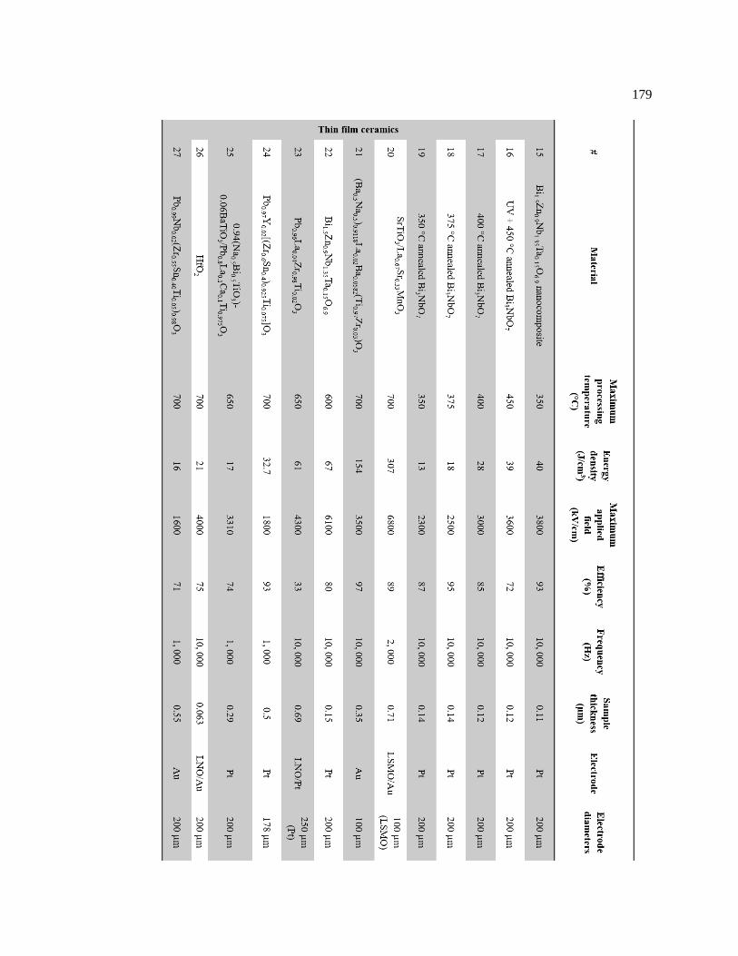
179
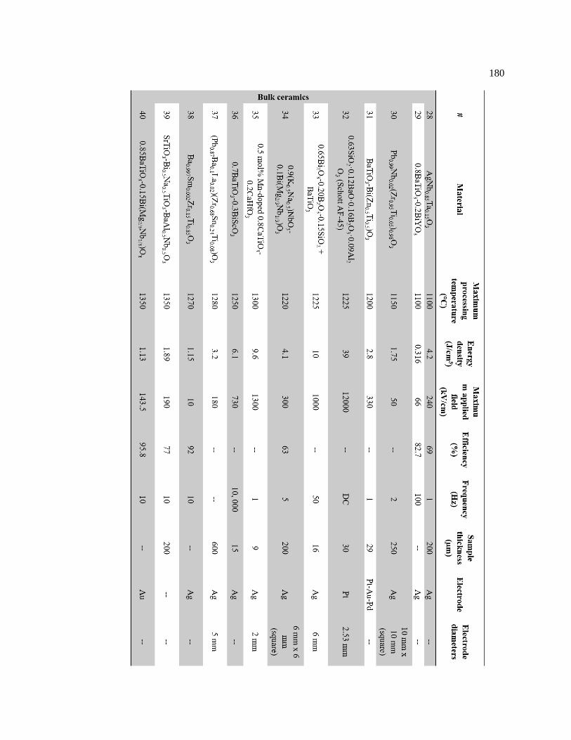
180
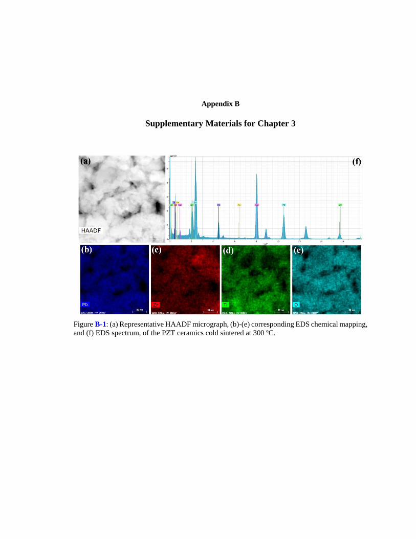
Appendix B
Supplementary Materials for Chapter 3
Figure B-1: (a) Representative HAADF micrograph, (b)-(e) corresponding EDS chemical mapping,
and (f) EDS spectrum, of the PZT ceramics cold sintered at 300 ºC.
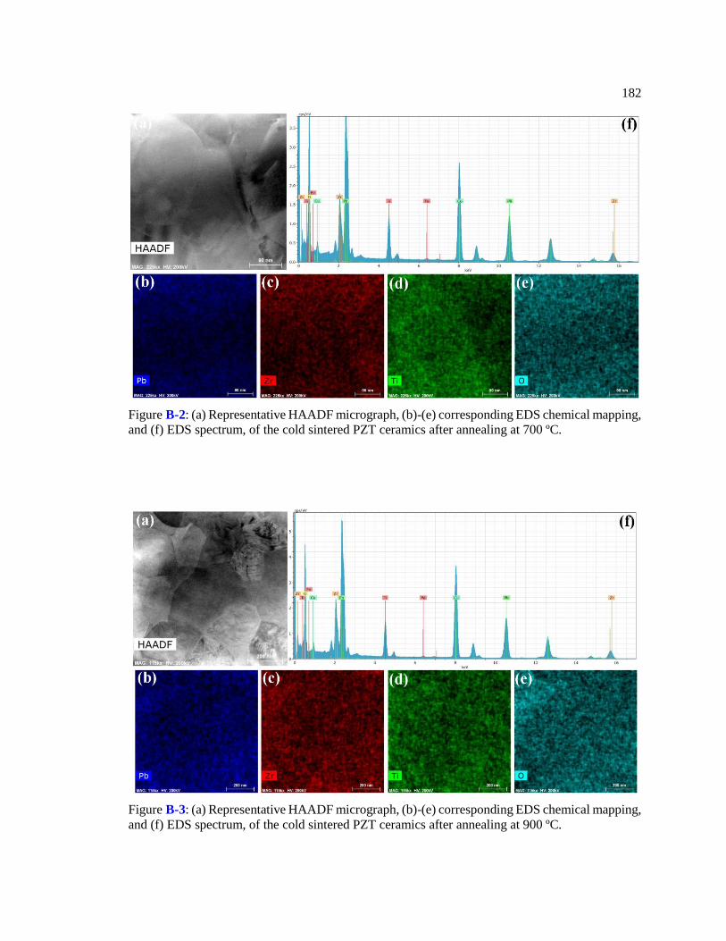
182
Figure B-2: (a) Representative HAADF micrograph, (b)-(e) corresponding EDS chemical mapping,
and (f) EDS spectrum, of the cold sintered PZT ceramics after annealing at 700 ºC.
Figure B-3: (a) Representative HAADF micrograph, (b)-(e) corresponding EDS chemical mapping,
and (f) EDS spectrum, of the cold sintered PZT ceramics after annealing at 900 ºC.
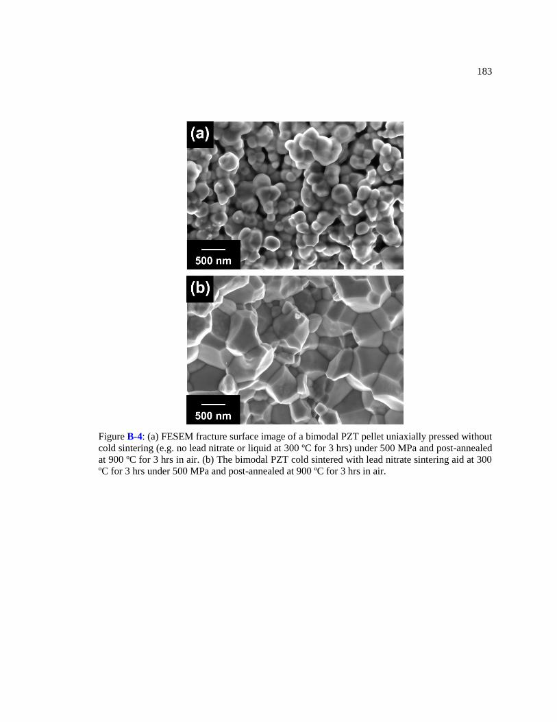
183
Figure B-4: (a) FESEM fracture surface image of a bimodal PZT pellet uniaxially pressed without
cold sintering (e.g. no lead nitrate or liquid at 300 ºC for 3 hrs) under 500 MPa and post-annealed
at 900 ºC for 3 hrs in air. (b) The bimodal PZT cold sintered with lead nitrate sintering aid at 300
ºC for 3 hrs under 500 MPa and post-annealed at 900 ºC for 3 hrs in air.
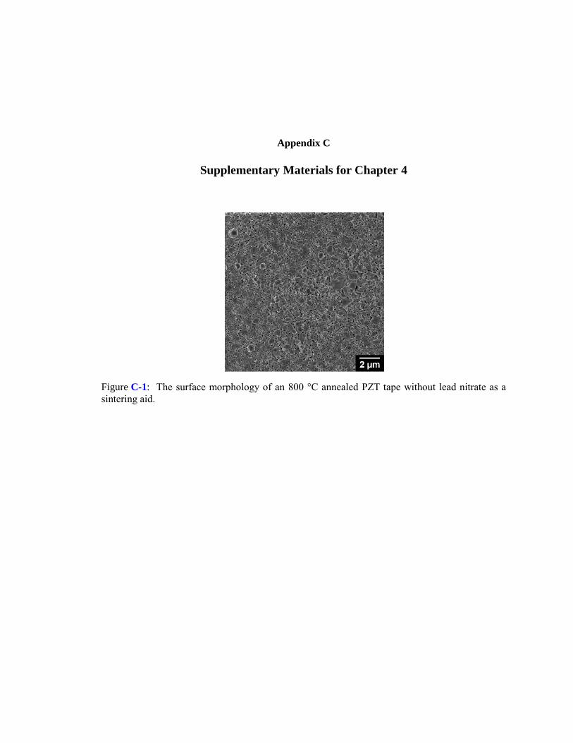
Appendix C
Supplementary Materials for Chapter 4
Figure C-1: The surface morphology of an 800 °C annealed PZT tape without lead nitrate as a
sintering aid.
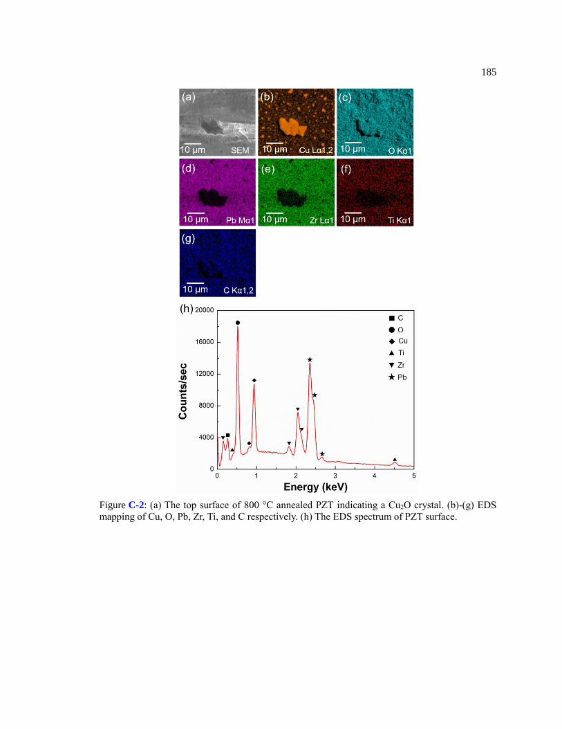
185
Figure C-2: (a) The top surface of 800 °C annealed PZT indicating a Cu2O crystal. (b)-(g) EDS
mapping of Cu, O, Pb, Zr, Ti, and C respectively. (h) The EDS spectrum of PZT surface.
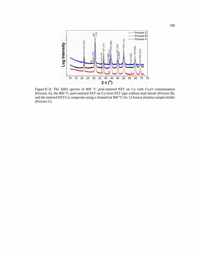
186
Figure C-3: The XRD spectra of 800 °C post-sintered PZT on Cu with Cu2O contamination
(Process A), the 800 °C post-sintered PZT on Cu from PZT tape without lead nitrate (Process B),
and the sintered PZT/Cu composite using a cleaned (at 900 °C for 12 hours) alumina sample holder
(Process C).
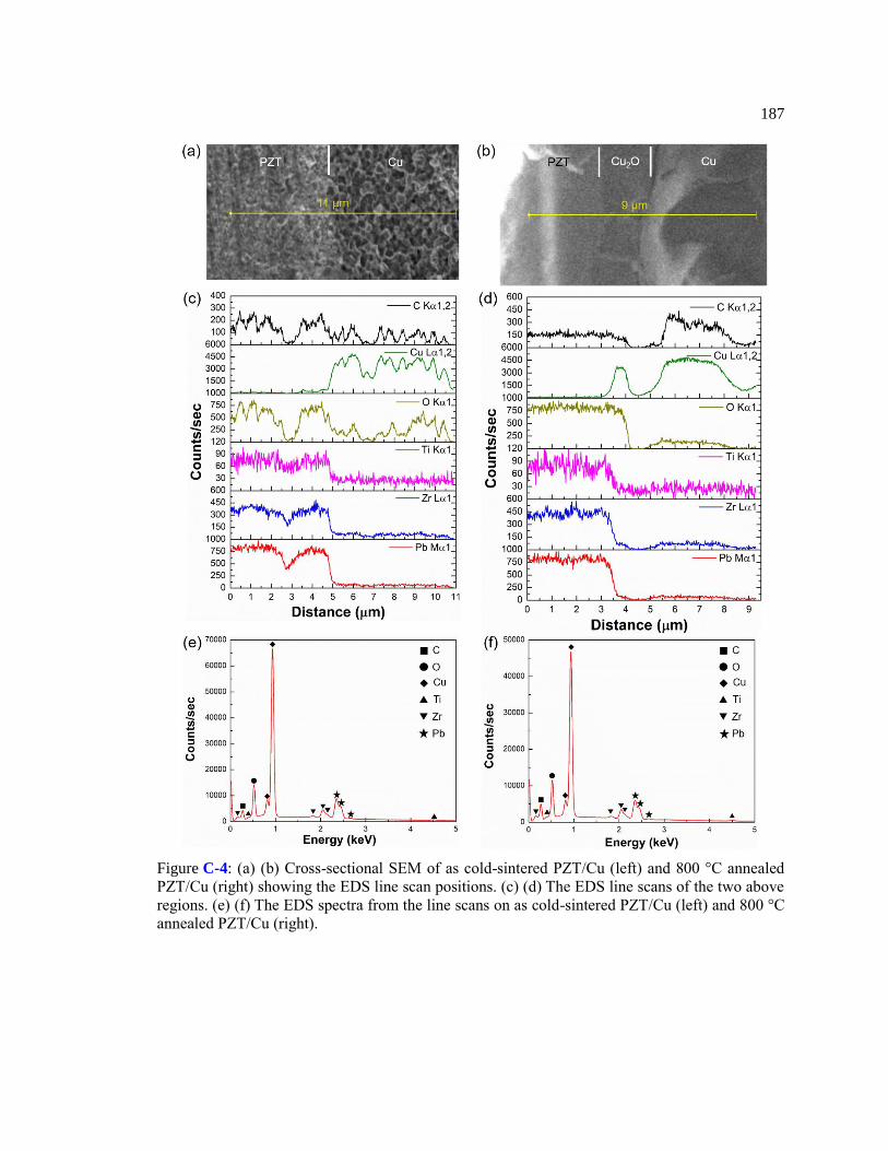
187
Figure C-4: (a) (b) Cross-sectional SEM of as cold-sintered PZT/Cu (left) and 800 °C annealed
PZT/Cu (right) showing the EDS line scan positions. (c) (d) The EDS line scans of the two above
regions. (e) (f) The EDS spectra from the line scans on as cold-sintered PZT/Cu (left) and 800 °C
annealed PZT/Cu (right).
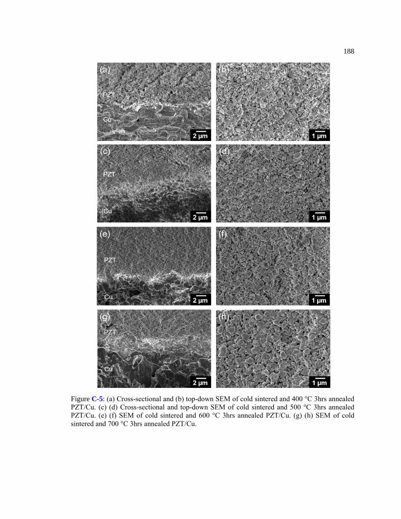
188
Figure C-5: (a) Cross-sectional and (b) top-down SEM of cold sintered and 400 °C 3hrs annealed
PZT/Cu. (c) (d) Cross-sectional and top-down SEM of cold sintered and 500 °C 3hrs annealed
PZT/Cu. (e) (f) SEM of cold sintered and 600 °C 3hrs annealed PZT/Cu. (g) (h) SEM of cold
sintered and 700 °C 3hrs annealed PZT/Cu.
VITA
Dixiong Wang
Dixiong Wang was born in Harbin, China in May 1992. He entered high school in 2008
during which he started to show interests in physics and chemistry. In 2011, he was admitted by
the Honor School of Harbin Institute of Technology (HIT) majoring in Materials Science and
Engineering. One year later, he became an undergraduate research assistant in Dr. Yaming
Wang’s group working on nitrogen and boron doped graphene nanosheet supercapacitor. He then
transferred to Pennsylvania State University (PSU) in 2013. In January 2014, he acquired his first
chemical vapor deposited graphene in Dr. Joshua Robinson’s lab. This study helped him
complete his B.S. degree at PSU and B.Eng. degree at HIT in 2015. From August 2015, he
continued to pursuit his doctorate degree in Dr. Susan Trolier-McKinstry’s group till today.
During this time, his research has focused on low temperature processing of dielectric/
piezoelectric thin films and ceramics.