Embed Size (px)
Citation preview
IEEE TRANSACTIONS ON POWER ELECTRONICS, VOL. 29, NO. 9, SEPTEMBER 2014 4733
A New Resonant Bidirectional DC–DCConverter Topology
Ross P. Twiname, Member, IEEE, Duleepa J. Thrimawithana, Member, IEEE, UdayaK. Madawala, Senior Member, IEEE, and Craig A. Baguley, Member, IEEE
Abstract—This paper presents a new resonant dual active bridge(DAB) topology, which uses a tuned inductor–capacitor–inductor(LCL) network. In comparison to conventional DAB topologies,the proposed topology significantly reduces the bridge currents,lowering both conduction and switching losses and the VA rat-ing associated with the bridges. The performance of the DAB isinvestigated using a mathematical model under various operat-ing conditions. Experimental results of a 2.5-kW prototype, whichhas an efficiency of 96% at rated power, are also presented withdiscussions to demonstrate the improved performance of the tunedLCL DAB topology. Results clearly indicate that the proposed DABtopology offers higher efficiency over a wide range of both inputvoltage and load in comparison to conventional DAB topologies.
Index Terms—Dual active bridge (DAB) converter, dc–dc con-verters, modulation, resonant converter.
I. INTRODUCTION
IN recent years, global concerns regarding future fossil fuelshortages have spurred efforts to reduce the reliance on oil,
coal, and gas to generate electricity. Consequently, electric-ity is increasingly generated from solar, wind, or tidal energysources [1]. These sources are renewable in nature, but highlyvariable, leading to the possibility of significant dynamic mis-matches between electricity supply and demand levels. How-ever, it has been proposed that the degree of mismatching canbe reduced through integrating the batteries of electric vehicles(EVs), which are not being used at any given time, into nationalelectric grid. This would provide a means for dynamic grid sta-bilization, but requires a bidirectional power interface betweenthe grid and EVs to allow vehicle-to-grid (V2G) energy transfersto take place [2]–[5].
Among the many types of bidirectional dc–dc converters thatcould be used in a V2G system, the DAB converter is a preferredoption, as it has a small component count, offers isolation, andallows for high power operation [6], [7]. In addition, it has theability to accommodate a wide range of voltage levels, as it
Manuscript received July 5, 2013; revised September 10, 2013; acceptedOctober 15, 2013. Date of current version April 30, 2014. Recommended forpublication by Associate Editor D. Xu.
R. P. Twiname and C. A. Baguley are with the Department of Electrical andElectronics Engineering, Auckland University of Technology, Auckland 1010,New Zealand (e-mail: [email protected]; [email protected]).
D. J. Thrimawithana and U. K. Madawala are with the Department ofElectrical and Computer Engineering, University of Auckland, Auckland1010, New Zealand (e-mail: [email protected]; [email protected]).
Color versions of one or more of the figures in this paper are available onlineat http://ieeexplore.ieee.org.
Digital Object Identifier 10.1109/TPEL.2013.2288325
may be controlled to operate in buck or boost modes. However,a conventional DAB converter using single phase-shift (SPS)control [8] draws a large reactive current component at low op-erating power levels, which increases the converter conductionlosses. This current component also necessitates the use of alarger dc-link capacitor [9], [10]. Therefore, various techniqueshave been used to lower the reactive current levels. In [11], pulsewidth modulation (PWM) of the higher voltage bridge was usedwith SPS to extend the zero-voltage-switching (ZVS) range toincrease the converter low-load efficiency, through a reductionin the reactive current. Triangular and trapezoidal modulationschemes were investigated in [12] in an effort to reduce thecurrent and, therefore, the conduction losses. Primarily, this re-sulted in a reduction in the switching losses by achieving zerocurrent switching in some of the switches [13]. In [14], the re-active power was reduced by using equal PWM on each bridge,as well as a phase shift between the bridges. Similar controltechniques to that in [11] were used in [15]–[17], except that thePWM was actively controlled by an algorithm. Bridge losseswere minimized in the former, while ZVS was extended to thefull operating range in the latter. However, the converter effi-ciencies in both cases were still limited for large differencesin the voltage conversion ratio, particularly under low poweroperating conditions. Rather than minimizing bridge losses, thefocus in [10] was the minimization of either the reactive power,or the rms, or peak current values, according to a selectablealgorithm. For this system, dual phase-shift control comprisingequal PWM of each bridge was used, as well as a phase shiftbetween the bridges. While each of the algorithms in [10] waseffective in improving the converter’s performance over that ofSPS, the resulting efficiency was less than 90% at full power,and notably less at low power. In an effort to reduce the rmscurrents and increase the ZVS range, independent PWM con-trol of each bridge, as well as a phase shift between the bridges,was employed in [18]. A composite modulation scheme wasproposed, whereby the control algorithm transitioned from dualPWM, at low phase-shift values, through to single PWM whichvaried linearly to a maximum for a phase-shift value of π/2 atfull power. This provided significant improvements in low-loadefficiency without a loss in the full-power capacity. For a dcconversion ratio of 2:1, the efficiency varied from 77% at a 3%load through to approximately 90% at full load. However, thisconverter required a more complicated control system than SPS.Furthermore, a number of resonant type DAB converter topolo-gies, consisting of series resonant networks, have been proposed.These topologies exhibit an extended soft-switching range andlower eddy current losses in the transformer windings, due to
0885-8993 © 2013 IEEE. Personal use is permitted, but republication/redistribution requires IEEE permission.See http://www.ieee.org/publications standards/publications/rights/index.html for more information.
4734 IEEE TRANSACTIONS ON POWER ELECTRONICS, VOL. 29, NO. 9, SEPTEMBER 2014
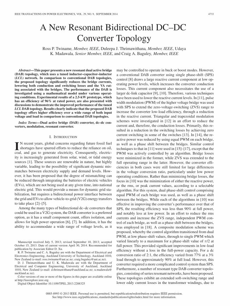
Fig. 1. Proposed resonant DAB converter.
improved current waveforms [19]–[22]. However, regardless ofthe control and resonant schemes employed, all existing DABconverter topologies inherently draw a large reactive currentcomponent at full power and, therefore, incur large conductionlosses.
This paper, therefore, proposes a novel DAB topology, whichutilizes a resonant network to minimize the reactive power re-quirement of the converter over the entire load range. The pro-posed converter employs a tuned inductor–capacitor–inductor(LCL) network, which includes the leakage inductance of theisolation transformer, to significantly reduce the magnitude ofbridge currents and, therefore, the switch and copper losses. Asimple control scheme is employed, where each bridge is drivenwith equal PWM while maintaining the phase shift between thebridges fixed at 90◦ or −90◦, to regulate the direction and mag-nitude of power flow. Theoretical analyses as well as simulatedresults are presented in comparison with experimental evidenceof a 2.5-kW prototype system, demonstrating the ability of theproposed topology to transfer bidirectional power at a high effi-ciency over a wide range of power and dc supply voltages.
II. PROPOSED TOPOLOGY
A schematic of the proposed resonant DAB converter isshown in Fig. 1, in which S1 − S8 represent semiconductorswitches. For simplicity, the active load on the secondary sideis represented by a voltage source, VDC2 . In practice, this volt-age source, which is connected to the output of the secondaryconverter, can be a battery pack used for storing or retrievingenergy. Furthermore, in a practical system, L2 may be incor-porated with the leakage inductance of the transformer ratherthan employing a discrete inductor. The primary side full-bridgeconverter, Bridge 1, of the proposed resonant DAB, is operatedat a fixed frequency, fs , and converts dc supply voltage VDC1to a three-level pulse-width-modulated ac voltage source v1 .Similarly, Bridge 2 is operated at the same frequency as the pri-mary and converts its dc supply voltage VDC2 to a pulse widthmodulated ac voltage source vB 2 . These two ac voltage sourcesare connected together through an isolation transformer and anL1C1L2 network, which is tuned to fs .
Traditional resonant DAB converters employ quasi-resonantnetworks, comprising inductors and capacitors to reduce switch-ing losses by improving the soft-switching range. These con-verters exhibit multiple operating or resonant modes within aswitching cycle, and typically complex modulation schemes
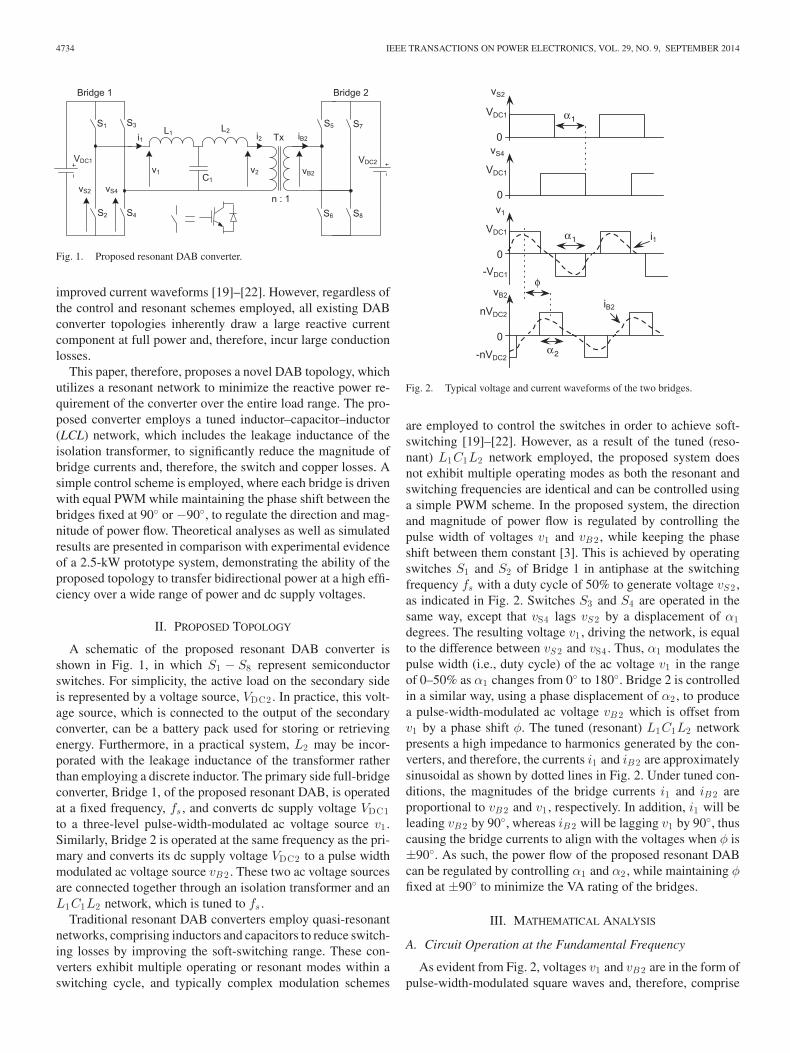
Fig. 2. Typical voltage and current waveforms of the two bridges.
are employed to control the switches in order to achieve soft-switching [19]–[22]. However, as a result of the tuned (reso-nant) L1C1L2 network employed, the proposed system doesnot exhibit multiple operating modes as both the resonant andswitching frequencies are identical and can be controlled usinga simple PWM scheme. In the proposed system, the directionand magnitude of power flow is regulated by controlling thepulse width of voltages v1 and vB 2 , while keeping the phaseshift between them constant [3]. This is achieved by operatingswitches S1 and S2 of Bridge 1 in antiphase at the switchingfrequency fs with a duty cycle of 50% to generate voltage vS2 ,as indicated in Fig. 2. Switches S3 and S4 are operated in thesame way, except that vS4 lags vS2 by a displacement of α1degrees. The resulting voltage v1 , driving the network, is equalto the difference between vS2 and vS4 . Thus, α1 modulates thepulse width (i.e., duty cycle) of the ac voltage v1 in the rangeof 0–50% as α1 changes from 0◦ to 180◦. Bridge 2 is controlledin a similar way, using a phase displacement of α2 , to producea pulse-width-modulated ac voltage vB 2 which is offset fromv1 by a phase shift φ. The tuned (resonant) L1C1L2 networkpresents a high impedance to harmonics generated by the con-verters, and therefore, the currents i1 and iB 2 are approximatelysinusoidal as shown by dotted lines in Fig. 2. Under tuned con-ditions, the magnitudes of the bridge currents i1 and iB 2 areproportional to vB 2 and v1 , respectively. In addition, i1 will beleading vB 2 by 90◦, whereas iB 2 will be lagging v1 by 90◦, thuscausing the bridge currents to align with the voltages when φ is±90◦. As such, the power flow of the proposed resonant DABcan be regulated by controlling α1 and α2 , while maintaining φfixed at ±90◦ to minimize the VA rating of the bridges.
III. MATHEMATICAL ANALYSIS
A. Circuit Operation at the Fundamental Frequency
As evident from Fig. 2, voltages v1 and vB 2 are in the form ofpulse-width-modulated square waves and, therefore, comprise
TWINAME et al.: NEW RESONANT BIDIRECTIONAL DC–DC >CONVERTER TOPOLOGY 4735
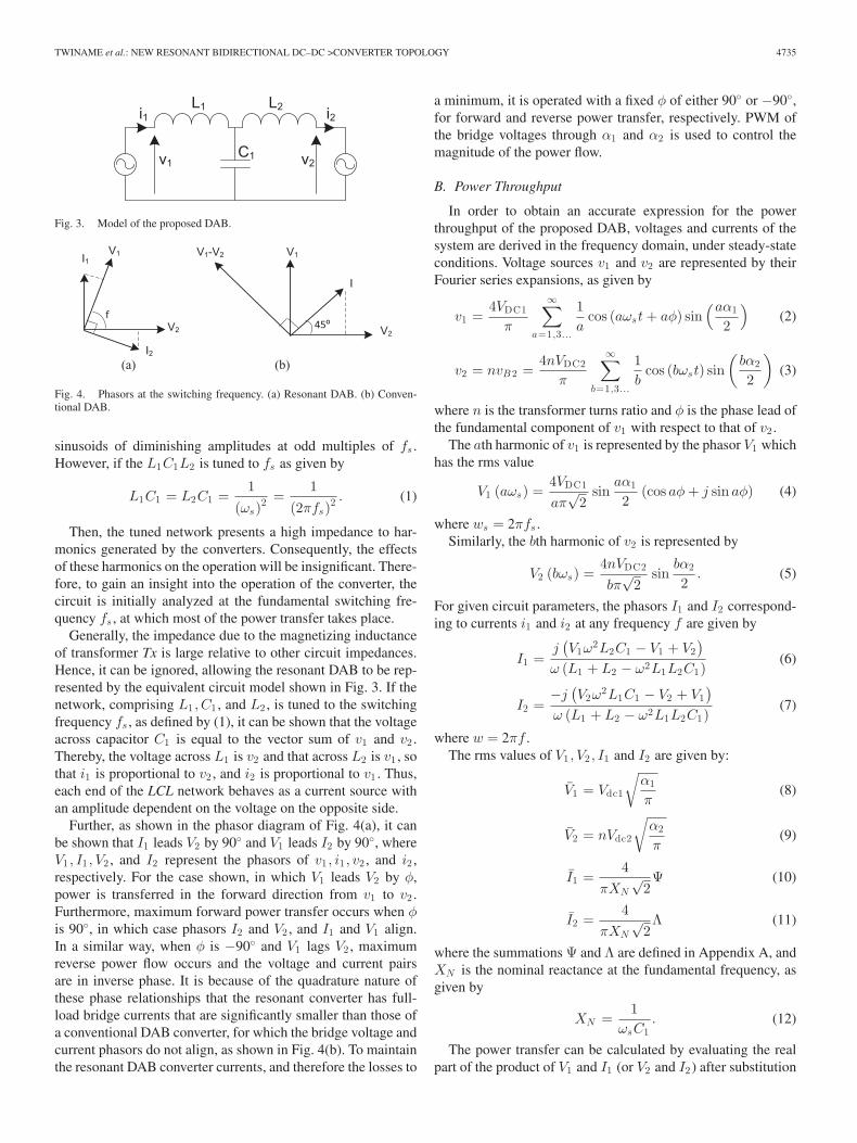
Fig. 3. Model of the proposed DAB.
(a) (b)
Fig. 4. Phasors at the switching frequency. (a) Resonant DAB. (b) Conven-tional DAB.
sinusoids of diminishing amplitudes at odd multiples of fs .However, if the L1C1L2 is tuned to fs as given by
L1C1 = L2C1 =1
(ωs)2 =
1(2πfs)
2 . (1)
Then, the tuned network presents a high impedance to har-monics generated by the converters. Consequently, the effectsof these harmonics on the operation will be insignificant. There-fore, to gain an insight into the operation of the converter, thecircuit is initially analyzed at the fundamental switching fre-quency fs , at which most of the power transfer takes place.
Generally, the impedance due to the magnetizing inductanceof transformer Tx is large relative to other circuit impedances.Hence, it can be ignored, allowing the resonant DAB to be rep-resented by the equivalent circuit model shown in Fig. 3. If thenetwork, comprising L1 , C1 , and L2 , is tuned to the switchingfrequency fs , as defined by (1), it can be shown that the voltageacross capacitor C1 is equal to the vector sum of v1 and v2 .Thereby, the voltage across L1 is v2 and that across L2 is v1 , sothat i1 is proportional to v2 , and i2 is proportional to v1 . Thus,each end of the LCL network behaves as a current source withan amplitude dependent on the voltage on the opposite side.
Further, as shown in the phasor diagram of Fig. 4(a), it canbe shown that I1 leads V2 by 90◦ and V1 leads I2 by 90◦, whereV1 , I1 , V2 , and I2 represent the phasors of v1 , i1 , v2 , and i2 ,respectively. For the case shown, in which V1 leads V2 by φ,power is transferred in the forward direction from v1 to v2 .Furthermore, maximum forward power transfer occurs when φis 90◦, in which case phasors I2 and V2 , and I1 and V1 align.In a similar way, when φ is −90◦ and V1 lags V2 , maximumreverse power flow occurs and the voltage and current pairsare in inverse phase. It is because of the quadrature nature ofthese phase relationships that the resonant converter has full-load bridge currents that are significantly smaller than those ofa conventional DAB converter, for which the bridge voltage andcurrent phasors do not align, as shown in Fig. 4(b). To maintainthe resonant DAB converter currents, and therefore the losses to
a minimum, it is operated with a fixed φ of either 90◦ or −90◦,for forward and reverse power transfer, respectively. PWM ofthe bridge voltages through α1 and α2 is used to control themagnitude of the power flow.
B. Power Throughput
In order to obtain an accurate expression for the powerthroughput of the proposed DAB, voltages and currents of thesystem are derived in the frequency domain, under steady-stateconditions. Voltage sources v1 and v2 are represented by theirFourier series expansions, as given by
v1 =4VDC1
π
∞∑
a=1,3...
1a
cos (aωst + aφ) sin(aα1
2
)(2)
v2 = nvB 2 =4nVDC2
π
∞∑
b=1,3...
1b
cos (bωst) sin(
bα2
2
)(3)
where n is the transformer turns ratio and φ is the phase lead ofthe fundamental component of v1 with respect to that of v2 .
The ath harmonic of v1 is represented by the phasor V1 whichhas the rms value
V1 (aωs) =4VDC1
aπ√
2sin
aα1
2(cos aφ + j sin aφ) (4)
where ws = 2πfs .Similarly, the bth harmonic of v2 is represented by
V2 (bωs) =4nVDC2
bπ√
2sin
bα2
2. (5)
For given circuit parameters, the phasors I1 and I2 correspond-ing to currents i1 and i2 at any frequency f are given by
I1 =j(V1ω
2L2C1 − V1 + V2)
ω (L1 + L2 − ω2L1L2C1)(6)
I2 =−j
(V2ω
2L1C1 − V2 + V1)
ω (L1 + L2 − ω2L1L2C1)(7)
where w = 2πf .The rms values of V1 , V2 , I1 and I2 are given by:
V1 = Vdc1
√α1
π(8)
V2 = nVdc2
√α2
π(9)
I1 =4
πXN
√2Ψ (10)
I2 =4
πXN
√2Λ (11)
where the summations Ψ and Λ are defined in Appendix A, andXN is the nominal reactance at the fundamental frequency, asgiven by
XN =1
ωsC1. (12)
The power transfer can be calculated by evaluating the realpart of the product of V1 and I1 (or V2 and I2) after substitution
4736 IEEE TRANSACTIONS ON POWER ELECTRONICS, VOL. 29, NO. 9, SEPTEMBER 2014
of (4) and (5) into (6) and (7), ignoring products of dissimilarfrequency components, and is given by
P = PN
∑
a=1,3...
sin(
aα12
)sin
(aα2
2
)sin aφ
a3(k1 + k2 − k1 k2
k3a2
) (13)
where factors k1 , k2 , and k3 represent the actual reactance valuesof L1 , L2 , and C1 , respectively, as a proportion of XN .
The constant PN is a function of the dc supply voltages,transformer turns ratio, and XN as given by
PN =8nVDC1VDC2
π2XN. (14)
According to (13), if the direction of power flow is con-trolled by setting φ to either 90◦ or −90◦, the magnitude of thepower transfer can be controlled with α1 and α2 . Under suchconditions, as per Section III-A, the bridge converters produceminimal reactive power as their fundamental voltage and currentcomponents are either in phase or in antiphase.
It is evident from (12)–(14) that the system parameters, oper-ating frequency, and supply voltages dictate the power through-put of the system for any given α1 and α2 . Thus, a proper insightinto the power transfer of the resonant DAB can only be obtainedby investigating the impact due to each of the above factors. Forthis reason, the system is analyzed by normalizing Vdc1 , nVdc2 ,and XN to unit values, which results in a normalized PN valueof 8/π2 ≈ 0.8106.
When the L1C1L2 network is tuned to the fundamentalswitching frequency, the denominator of (13) increases rapidlyfor higher harmonics. For example, its value is 1 at the funda-mental frequency and 189, 2875, and 16121 at the third, fifth,and seventh harmonics, respectively. Hence, the fundamentalis the only significant component in (13), as expected, in viewof the tuned nature of the network. At maximum modulation,with α1 and α2 equal to 180◦ and φ of ±90◦, the summation in(13) is equal to 1.005, so that the normalized maximum powertransfer is 0.8146. This is comparable to the factor of 0.7854which applies for a conventional DAB [23].
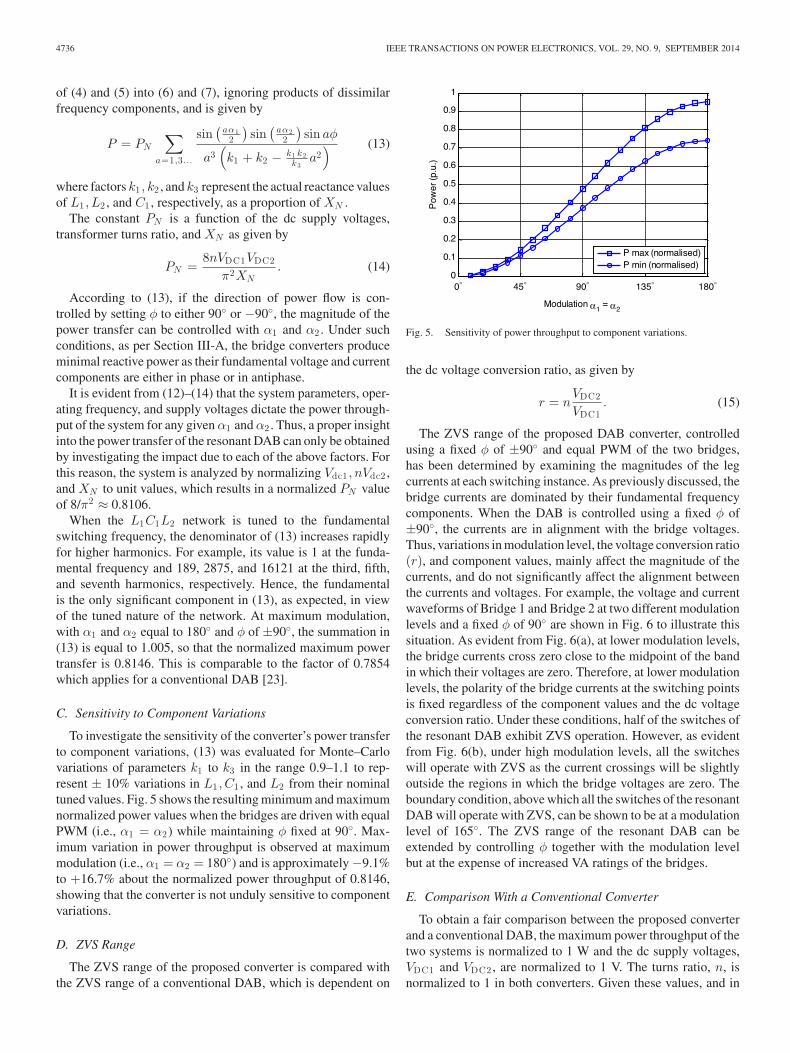
C. Sensitivity to Component Variations
To investigate the sensitivity of the converter’s power transferto component variations, (13) was evaluated for Monte–Carlovariations of parameters k1 to k3 in the range 0.9–1.1 to rep-resent ± 10% variations in L1 , C1 , and L2 from their nominaltuned values. Fig. 5 shows the resulting minimum and maximumnormalized power values when the bridges are driven with equalPWM (i.e., α1 = α2) while maintaining φ fixed at 90◦. Max-imum variation in power throughput is observed at maximummodulation (i.e., α1 = α2 = 180◦) and is approximately −9.1%to +16.7% about the normalized power throughput of 0.8146,showing that the converter is not unduly sensitive to componentvariations.
D. ZVS Range
The ZVS range of the proposed converter is compared withthe ZVS range of a conventional DAB, which is dependent on
Fig. 5. Sensitivity of power throughput to component variations.
the dc voltage conversion ratio, as given by
r = nVDC2
VDC1. (15)
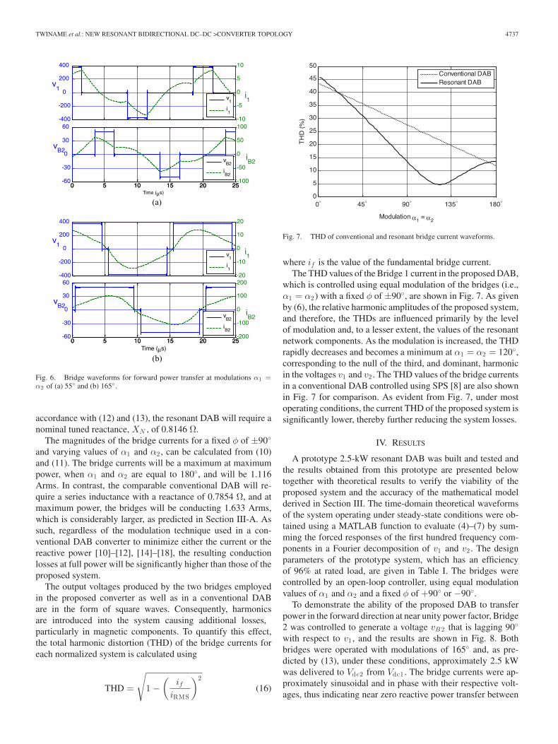
The ZVS range of the proposed DAB converter, controlledusing a fixed φ of ±90◦ and equal PWM of the two bridges,has been determined by examining the magnitudes of the legcurrents at each switching instance. As previously discussed, thebridge currents are dominated by their fundamental frequencycomponents. When the DAB is controlled using a fixed φ of±90◦, the currents are in alignment with the bridge voltages.Thus, variations in modulation level, the voltage conversion ratio(r), and component values, mainly affect the magnitude of thecurrents, and do not significantly affect the alignment betweenthe currents and voltages. For example, the voltage and currentwaveforms of Bridge 1 and Bridge 2 at two different modulationlevels and a fixed φ of 90◦ are shown in Fig. 6 to illustrate thissituation. As evident from Fig. 6(a), at lower modulation levels,the bridge currents cross zero close to the midpoint of the bandin which their voltages are zero. Therefore, at lower modulationlevels, the polarity of the bridge currents at the switching pointsis fixed regardless of the component values and the dc voltageconversion ratio. Under these conditions, half of the switches ofthe resonant DAB exhibit ZVS operation. However, as evidentfrom Fig. 6(b), under high modulation levels, all the switcheswill operate with ZVS as the current crossings will be slightlyoutside the regions in which the bridge voltages are zero. Theboundary condition, above which all the switches of the resonantDAB will operate with ZVS, can be shown to be at a modulationlevel of 165◦. The ZVS range of the resonant DAB can beextended by controlling φ together with the modulation levelbut at the expense of increased VA ratings of the bridges.
E. Comparison With a Conventional Converter
To obtain a fair comparison between the proposed converterand a conventional DAB, the maximum power throughput of thetwo systems is normalized to 1 W and the dc supply voltages,VDC1 and VDC2 , are normalized to 1 V. The turns ratio, n, isnormalized to 1 in both converters. Given these values, and in
TWINAME et al.: NEW RESONANT BIDIRECTIONAL DC–DC >CONVERTER TOPOLOGY 4737
(a)
(b)
Fig. 6. Bridge waveforms for forward power transfer at modulations α1 =α2 of (a) 55◦ and (b) 165◦.
accordance with (12) and (13), the resonant DAB will require anominal tuned reactance, XN , of 0.8146 Ω.
The magnitudes of the bridge currents for a fixed φ of ±90◦
and varying values of α1 and α2 , can be calculated from (10)and (11). The bridge currents will be a maximum at maximumpower, when α1 and α2 are equal to 180◦, and will be 1.116Arms. In contrast, the comparable conventional DAB will re-quire a series inductance with a reactance of 0.7854 Ω, and atmaximum power, the bridges will be conducting 1.633 Arms,which is considerably larger, as predicted in Section III-A. Assuch, regardless of the modulation technique used in a con-ventional DAB converter to minimize either the current or thereactive power [10]–[12], [14]–[18], the resulting conductionlosses at full power will be significantly higher than those of theproposed system.
The output voltages produced by the two bridges employedin the proposed converter as well as in a conventional DABare in the form of square waves. Consequently, harmonicsare introduced into the system causing additional losses,particularly in magnetic components. To quantify this effect,the total harmonic distortion (THD) of the bridge currents foreach normalized system is calculated using
THD =
√
1 −(
ifiRMS
)2
(16)
Fig. 7. THD of conventional and resonant bridge current waveforms.
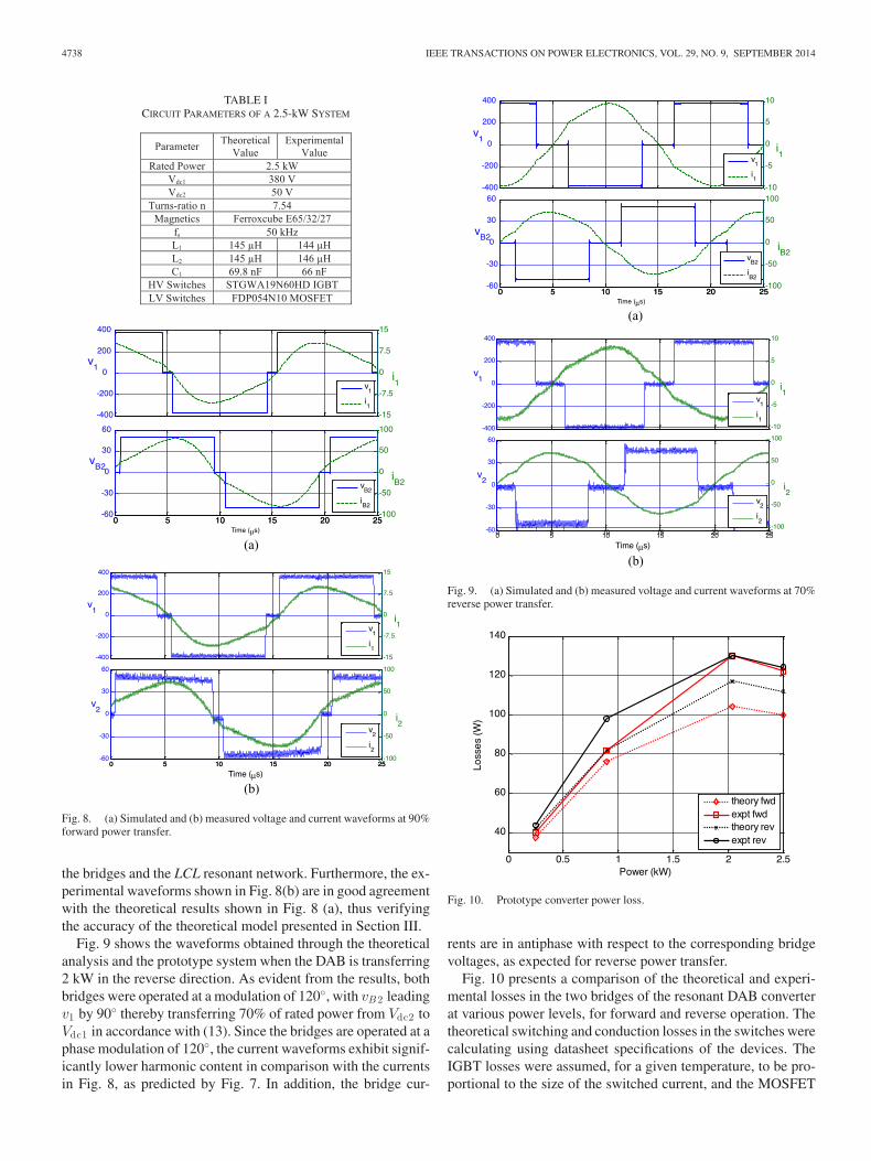
where if is the value of the fundamental bridge current.The THD values of the Bridge 1 current in the proposed DAB,
which is controlled using equal modulation of the bridges (i.e.,α1 = α2) with a fixed φ of ±90◦, are shown in Fig. 7. As givenby (6), the relative harmonic amplitudes of the proposed system,and therefore, the THDs are influenced primarily by the levelof modulation and, to a lesser extent, the values of the resonantnetwork components. As the modulation is increased, the THDrapidly decreases and becomes a minimum at α1 = α2 = 120◦,corresponding to the null of the third, and dominant, harmonicin the voltages v1 and v2 . The THD values of the bridge currentsin a conventional DAB controlled using SPS [8] are also shownin Fig. 7 for comparison. As evident from Fig. 7, under mostoperating conditions, the current THD of the proposed system issignificantly lower, thereby further reducing the system losses.
IV. RESULTS
A prototype 2.5-kW resonant DAB was built and tested andthe results obtained from this prototype are presented belowtogether with theoretical results to verify the viability of theproposed system and the accuracy of the mathematical modelderived in Section III. The time-domain theoretical waveformsof the system operating under steady-state conditions were ob-tained using a MATLAB function to evaluate (4)–(7) by sum-ming the forced responses of the first hundred frequency com-ponents in a Fourier decomposition of v1 and v2 . The designparameters of the prototype system, which has an efficiencyof 96% at rated load, are given in Table I. The bridges werecontrolled by an open-loop controller, using equal modulationvalues of α1 and α2 and a fixed φ of +90◦ or −90◦.
To demonstrate the ability of the proposed DAB to transferpower in the forward direction at near unity power factor, Bridge2 was controlled to generate a voltage vB 2 that is lagging 90◦
with respect to v1 , and the results are shown in Fig. 8. Bothbridges were operated with modulations of 165◦ and, as pre-dicted by (13), under these conditions, approximately 2.5 kWwas delivered to Vdc2 from Vdc1 . The bridge currents were ap-proximately sinusoidal and in phase with their respective volt-ages, thus indicating near zero reactive power transfer between
4738 IEEE TRANSACTIONS ON POWER ELECTRONICS, VOL. 29, NO. 9, SEPTEMBER 2014
TABLE ICIRCUIT PARAMETERS OF A 2.5-kW SYSTEM
(a)
(b)
Fig. 8. (a) Simulated and (b) measured voltage and current waveforms at 90%forward power transfer.
the bridges and the LCL resonant network. Furthermore, the ex-perimental waveforms shown in Fig. 8(b) are in good agreementwith the theoretical results shown in Fig. 8 (a), thus verifyingthe accuracy of the theoretical model presented in Section III.
Fig. 9 shows the waveforms obtained through the theoreticalanalysis and the prototype system when the DAB is transferring2 kW in the reverse direction. As evident from the results, bothbridges were operated at a modulation of 120◦, with vB 2 leadingv1 by 90◦ thereby transferring 70% of rated power from Vdc2 toVdc1 in accordance with (13). Since the bridges are operated at aphase modulation of 120◦, the current waveforms exhibit signif-icantly lower harmonic content in comparison with the currentsin Fig. 8, as predicted by Fig. 7. In addition, the bridge cur-
(a)
(b)
Fig. 9. (a) Simulated and (b) measured voltage and current waveforms at 70%reverse power transfer.
Fig. 10. Prototype converter power loss.
rents are in antiphase with respect to the corresponding bridgevoltages, as expected for reverse power transfer.
Fig. 10 presents a comparison of the theoretical and experi-mental losses in the two bridges of the resonant DAB converterat various power levels, for forward and reverse operation. Thetheoretical switching and conduction losses in the switches werecalculating using datasheet specifications of the devices. TheIGBT losses were assumed, for a given temperature, to be pro-portional to the size of the switched current, and the MOSFET
TWINAME et al.: NEW RESONANT BIDIRECTIONAL DC–DC >CONVERTER TOPOLOGY 4739
Fig. 11. Prototype system efficiency.
losses were calculated according to [24]. A slight discrepancybetween the measured losses and theoretical losses can be ob-served. However, agreement exists in the trends, including thedip in the losses for power levels above 2 kW correspondingto modulation levels above 165◦, at which there is a decreasein the switching losses. As evident from Fig. 6, the number oflegs having ZVS goes from 2 to 4, as the modulation increasesabove 165◦, and therefore, the losses are expected to be lowerwhen α1 and α2 are greater than 165◦. The theoretical calcula-tions further show that at full power, the conduction losses areapproximately 80% of the total losses. Although this propor-tion will, in general, depend on the particular devices used, itjustifies efforts to reduce conduction losses and emphasizes theadvantage of the proposed resonant DAB converter.
The experimental and theoretical efficiency values, each ofwhich includes the power losses in the magnetic components aswell as those from the switching devices, are shown in Fig. 11.Although the prototype DAB presented in this paper has notbeen optimized for efficiency, as it was purely developed as aproof of concept system, the results suggest a significant im-provement in the performance in comparison to conventionalDAB converters with SPS control. In addition, even higher ef-ficiencies are likely to be obtained if the Bridge 2 voltage isincreased, avoiding the relatively large conduction losses in thesecondary part of the circuit. As evident from Fig. 11, boththe theoretical and experimental efficiencies are in good agree-ment. As such, the mathematical analysis presented can be usedto accurately characterize the losses in a resonant DAB undervarious operating conditions and accounting for variations incomponent values.
V. CONCLUSION
A new dual DAB topology that employs an LCL resonantnetwork has been described. A mathematical model has beenpresented to accurately predict the performance of the proposedtopology. Experimental results of a 2.5-kW prototype DAB, op-erated under various conditions, have also been presented todemonstrate the improved performance of the converter. Re-sults indicate that the proposed DAB topology has lower bridge
currents and, consequently, offers higher efficiency over a widersupply voltage and load range in comparison to conventionalDAB topologies.
APPENDIX A
ψ =√√√√√√√√√√
∑
m =1 ,3 . . .
(nVdc2 sin m α 2
2 + Vdc1 sin m α 12 cos mφ
(k 2k 3
m2 − 1))2
+(Vdc1 sin m α 1
2 sin mφ(
k 2k 3
m2 − 1))2
(m2
(k1 + k2 − k 1 k 2
k 3m2
))2
Λ =√√√√√√√√√
∑
m =1 ,3 . . .
(Vdc1 sin m α 1
2 cos mφ + nVdc2 sin m α 22
(k 1k 3
m2 − 1))2
+(Vdc1 sin m α 1
2 sin mφ)2
(m2
(k1 + k2 − k 1 k 2
k 3m2
))2 .
REFERENCES
[1] J. Marsden, “Distributed generation systems: A new paradigm for sustain-able energy,” in Proc. IEEE Green Technol. Conf., 2011, pp. 1–4.
[2] B. Kramer, S. Chakraborty, and B. Kroposki, “A review of plug-in vehiclesand vehicle-to-grid capability,” in Proc. IEEE Conf. Ind. Electron., 2008,pp. 2278–2283.
[3] U. K. Madawala and D. J. Thrimawithana, “A bidirectional inductivepower interface for electric vehicles in V2G systems,” IEEE Trans. Ind.Electron., vol. 58, no. 10, pp. 4789–4796, Oct. 2011.
[4] D. J. Thrimawithana and U. K. Madawala, “A model for a multi-sourcedgreen energy system,” in Proc. IEEE Conf. Sustainable Energy Technol.,2010, pp. 1–6.
[5] N. D. Weise, K. K. Mohapatra, and N. Mohan, “Universal utility interfacefor plug-in hybrid electric vehicles with vehicle-to-grid functionality,” inProc. IEEE Power Energy Soc. Gen. Meeting, 2010, pp. 1–8.
[6] R. L. Steigerwald, R. W. De Doncker, and H. Kheraluwala, “A comparisonof high-power DC-DC soft-switched converter topologies,” IEEE Trans.Ind. Appl., vol. 32, no. 5, pp. 1139–1145, Sep./Oct. 1996.
[7] D. Yu, S. Lukic, B. Jacobson, and A. Huang, “Review of high powerisolated bi-directional DC-DC converters for PHEV/EV DC charging in-frastructure,” in Proc. IEEE Energy Convers. Congr. Expo., 2011, pp. 553–560.
[8] R. W. A. A. De Doncker, D. M. Divan, and M. H. Kheraluwala, “A three-phase soft-switched high-power-density DC-DC converter for high-powerapplications,” IEEE Trans. Ind. Appl., vol. 27, no. 1, pp. 63–73, Jan./Feb.1991.
[9] B. Hua, N. Ziling, and C. C. Mi, “Experimental comparison of traditionalphase-shift, dual-phase-shift, and model-based control of isolated bidirec-tional DC-DC converters,” IEEE Trans. Power Electron., vol. 25, no. 6,pp. 1444–1449, Jun. 2010.
[10] K. Myoungho, M. Rosekeit, S. Seung-Ki, and R. W. A. A. De Doncker, “Adual-phase-shift control strategy for dual-active-bridge DC-DC converterin wide voltage range,” in Proc. IEEE Power Electron. Energy Convers.Congr. Expo. Asia, 2011, pp. 364–371.
[11] G. G. Oggier, R. Ledhold, G. O. Garcia, A. R. Olivia, J. C. Blaba, andF. Barlow, “Extending the ZVS operating range of dual active bridgehigh-power DC-DC converters,” in Proc. IEEE Power Electron. Spec.Conf., 2006, pp. 1–7.
[12] F. Krismer, S. Round, and J. W. Kolar, “Performance optimization of ahigh current dual active bridge with a wide operating voltage range,” inProc. IEEE Power Electron. Spec. Conf., 2006, pp. 1–7.
[13] R. L. Steigerwald, “A review of soft-switching techniques in high perfor-mance DC power supplies,” in Proc. IEEE Conf. Ind. Electron. ControlInstrum., 1995, pp. 1–7.
[14] B. Hua and C. Mi, “Eliminate reactive power and increase system ef-ficiency of isolated bidirectional dual-active-bridge DC-DC converters

4740 IEEE TRANSACTIONS ON POWER ELECTRONICS, VOL. 29, NO. 9, SEPTEMBER 2014
using novel dual-phase-shift control,” IEEE Trans. Power Electron.,vol. 23, no. 6, pp. 2905–2914, Nov. 2008.
[15] G. G. Oggier, G. O. Garcia, and A. R. Oliva, “Switching control strategyto minimize dual active bridge converter losses,” IEEE Trans. PowerElectron., vol. 24, no. 7, pp. 1826–1838, Jul. 2009.
[16] B. Zhao, Q. Song, and W. Liu, “Efficiency characterization and optimiza-tion of isolated bidirectional DC-DC converter based on dual-phase-shiftcontrol for DC distribution application,” IEEE Trans. Power Electron.,vol. 28, no. 4, pp. 1711–1727, Apr. 2013.
[17] G. G. Oggier, G. O. Garci, and A. R. Oliva, “Modulation strategy to op-erate the dual active bridge DC-DC converter under soft switching inthe whole operating range,” IEEE Trans. Power Electron., vol. 26, no. 4,pp. 1228–1236, Apr. 2011.
[18] A. K. Jain and R. Ayyanar, “PWM control of dual active bridge: Com-prehensive analysis and experimental verification,” IEEE Trans. PowerElectron., vol. 26, no. 4, pp. 1215–1227, Apr. 2011.
[19] R. Lenke, F. Mura, and R. W. A. De Doncker, “Comparison of non-resonant and super-resonant dual-active ZVS-operated high-power DC-DC converters,” in Proc. IEEE Conf. Power Electron. Appl., 2009, pp. 1–10.
[20] C. Wei, S. Wang, X. Hong, Z. Lu, and S. Ye, “Fully soft-switched bidi-rectional resonant dc-dc converter with a new CLLC tank,” in Proc. IEEEAppl. Power Electron. Conf. Expo., 2010, pp. 1238–1241.
[21] L. Corradini, D. Seltzer, D. Bloomquist, R. Zane, D. Maksimovic, andB. Jacobson, “Minimum current operation of bidirectional dual-bridgeseries resonant DC/DC converters,” IEEE Trans. Power Electron., vol. 27,no. 7, pp. 3266–3276, Jul. 2012.
[22] Z. Pavlovic, J. A. Oliver, P. Alou, O. Garcia, and J. A. Cobos, “Bidirec-tional dual active bridge series resonant converter with pulse modula-tion,” in Proc. 27th Annu. IEEE Appl. Power Electron. Conf. Expo., 2012,pp. 503–508.
[23] M. N. Kheraluwala, “Performance characterisation of a high-power dualactive bridge DC-to-DC converter,” IEEE Trans. Ind. Appl., vol. 28, no. 6,pp. 1294–1301, Nov./Dec. 1992.
[24] D. D. Graovac, M. Purschel, and A. Kiep. (2012, Dec.). MOSFET powerlosses calculation using the data-sheet parameters. [Online]. Available:http://notes-application.abcelectronique.com/070/70–41484.pdf
Ross P. Twiname (M’06) received the B.E. degree inelectrical engineering from the University of Auck-land, Auckland, New Zealand, in 1975.
After a number of years in the industry, he joinedthe Department of Electrical and Electronic Engineer-ing, Auckland University of Technology Auckland,where he is currently a Senior Lecturer. His researchinterests include electronic applications and powerconversion.
Duleepa J. Thrimawithana (M’09) received theB.E. degree (with first-class honors) in electrical en-gineering and the Ph.D. degree in power electronicsfrom the University of Auckland, Auckland, NewZealand, in 2005 and 2009, respectively.
From 2005 to 2008, he worked, in collaborationwith Tru-Test Ltd., Auckland, New Zealand, as a Re-search Engineer in the areas of power converters andhigh-voltage pulse generator design. He is currentlyworking as a Senior Lecturer at the Department ofElectrical and Computer Engineering, University of
Auckland. His main research interests include the fields of inductive powertransfer, power electronics, and renewable energy.
Udaya K. Madawala (M’95–SM’06) received theB.Sc. (Hons.) degree in electrical engineering fromthe University of Moratuwa, Moratuwa, Sri Lanka, in1987, and the Ph.D. degree in power electronics fromthe University of Auckland, Auckland, New Zealand,in 1993.
After working in industry, he joined the Depart-ment of Electrical and Computer Engineering, TheUniversity of Auckland, as a Research Fellow in1997, where he is currently an Associate Professor.His research interests are in the fields of power elec-
tronics, inductive power transfer, and renewable energy.
Craig A. Baguley (M’12) received the Ph.D. degreefrom the University of Auckland, Auckland, NewZealand, in 2011.
Previously, he has been employed as a Design En-gineer in the fields of power electronics and magneticcomponent design. He is currently employed by theAuckland University of Technology, Auckland. Hisresearch interests include magnetic component de-sign and modeling, induction heating, and the designof high-current converters.