Embed Size (px)
Citation preview
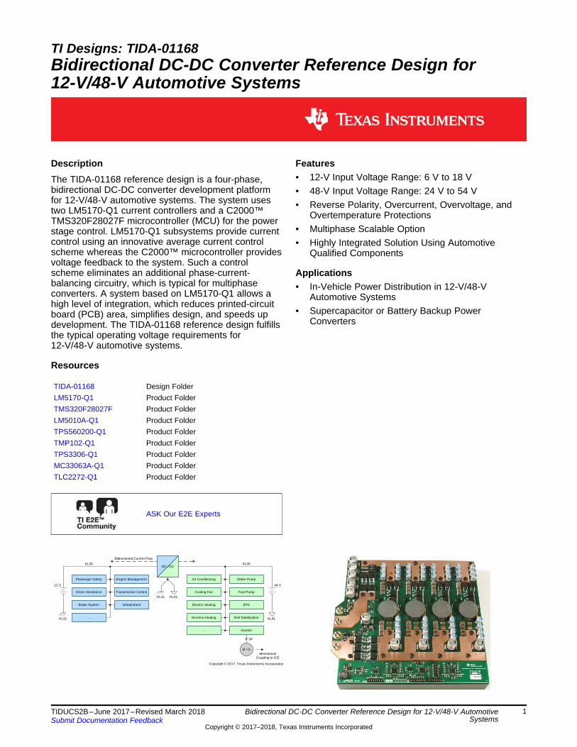
KL31
Passenger Safety
Driver Assistance
Brake System
Engine Management
Transmission Control
Infotainment
...
Air Conditioning
Cooling Fan
Electric Heating
Water Pump
Fuel Pump
EPS
...
Screens Heating Roll Stabilization
Inverter
Bidirectional Current Flow
M / GMechanical
Coupling to ICE
KL41
3P
KL41KL31
DC / DCKL30 KL40
12 V 48 V
Copyright © 2017, Texas Instruments Incorporated
1TIDUCS2B–June 2017–Revised March 2018Submit Documentation Feedback
Copyright © 2017–2018, Texas Instruments Incorporated
Bidirectional DC-DC Converter Reference Design for 12-V/48-V AutomotiveSystems
TI Designs: TIDA-01168Bidirectional DC-DC Converter Reference Design for12-V/48-V Automotive Systems
DescriptionThe TIDA-01168 reference design is a four-phase,bidirectional DC-DC converter development platformfor 12-V/48-V automotive systems. The system usestwo LM5170-Q1 current controllers and a C2000™TMS320F28027F microcontroller (MCU) for the powerstage control. LM5170-Q1 subsystems provide currentcontrol using an innovative average current controlscheme whereas the C2000™ microcontroller providesvoltage feedback to the system. Such a controlscheme eliminates an additional phase-current-balancing circuitry, which is typical for multiphaseconverters. A system based on LM5170-Q1 allows ahigh level of integration, which reduces printed-circuitboard (PCB) area, simplifies design, and speeds updevelopment. The TIDA-01168 reference design fulfillsthe typical operating voltage requirements for12-V/48-V automotive systems.
Resources
TIDA-01168 Design FolderLM5170-Q1 Product FolderTMS320F28027F Product FolderLM5010A-Q1 Product FolderTPS560200-Q1 Product FolderTMP102-Q1 Product FolderTPS3306-Q1 Product FolderMC33063A-Q1 Product FolderTLC2272-Q1 Product Folder
ASK Our E2E Experts
Features• 12-V Input Voltage Range: 6 V to 18 V• 48-V Input Voltage Range: 24 V to 54 V• Reverse Polarity, Overcurrent, Overvoltage, and
Overtemperature Protections• Multiphase Scalable Option• Highly Integrated Solution Using Automotive
Qualified Components
Applications• In-Vehicle Power Distribution in 12-V/48-V
Automotive Systems• Supercapacitor or Battery Backup Power
Converters
Discharge Capacity [%]
Vcell [V]
4.2
0.025 50 75 100
1C
2C
Copyright © 2017, Texas Instruments Incorporated
DC - DC
Battery 1
RS
I
CDCLINK M / G
Three-phase Inverter
Battery 2
RS
Copyright © 2017, Texas Instruments Incorporated
TIDA-01168
System Description www.ti.com
2 TIDUCS2B–June 2017–Revised March 2018Submit Documentation Feedback
Copyright © 2017–2018, Texas Instruments Incorporated
Bidirectional DC-DC Converter Reference Design for 12-V/48-V AutomotiveSystems
An IMPORTANT NOTICE at the end of this TI reference design addresses authorized use, intellectual property matters and otherimportant disclaimers and information.
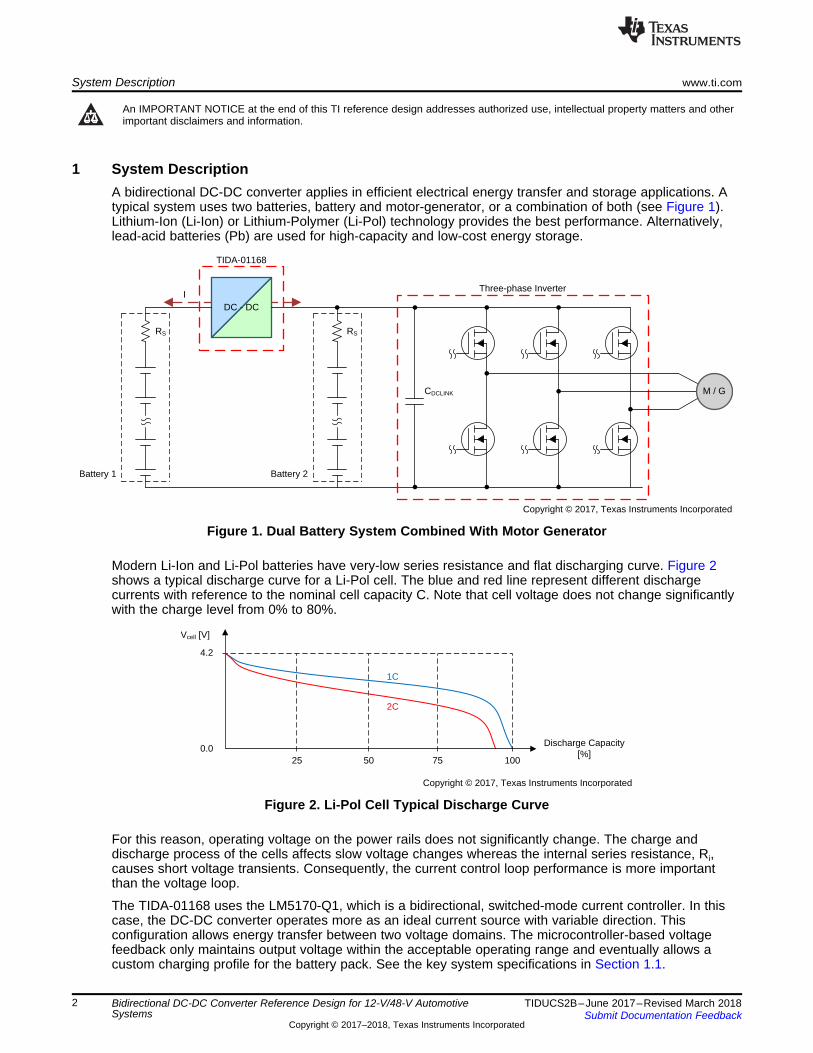
1 System DescriptionA bidirectional DC-DC converter applies in efficient electrical energy transfer and storage applications. Atypical system uses two batteries, battery and motor-generator, or a combination of both (see Figure 1).Lithium-Ion (Li-Ion) or Lithium-Polymer (Li-Pol) technology provides the best performance. Alternatively,lead-acid batteries (Pb) are used for high-capacity and low-cost energy storage.
Figure 1. Dual Battery System Combined With Motor Generator
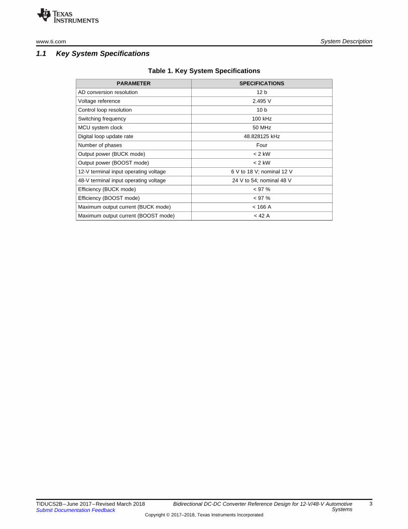
Modern Li-Ion and Li-Pol batteries have very-low series resistance and flat discharging curve. Figure 2shows a typical discharge curve for a Li-Pol cell. The blue and red line represent different dischargecurrents with reference to the nominal cell capacity C. Note that cell voltage does not change significantlywith the charge level from 0% to 80%.
Figure 2. Li-Pol Cell Typical Discharge Curve
For this reason, operating voltage on the power rails does not significantly change. The charge anddischarge process of the cells affects slow voltage changes whereas the internal series resistance, Ri,causes short voltage transients. Consequently, the current control loop performance is more importantthan the voltage loop.
The TIDA-01168 uses the LM5170-Q1, which is a bidirectional, switched-mode current controller. In thiscase, the DC-DC converter operates more as an ideal current source with variable direction. Thisconfiguration allows energy transfer between two voltage domains. The microcontroller-based voltagefeedback only maintains output voltage within the acceptable operating range and eventually allows acustom charging profile for the battery pack. See the key system specifications in Section 1.1.
www.ti.com System Description
3TIDUCS2B–June 2017–Revised March 2018Submit Documentation Feedback
Copyright © 2017–2018, Texas Instruments Incorporated
Bidirectional DC-DC Converter Reference Design for 12-V/48-V AutomotiveSystems
1.1 Key System Specifications
Table 1. Key System Specifications
PARAMETER SPECIFICATIONSAD conversion resolution 12 bVoltage reference 2.495 VControl loop resolution 10 bSwitching frequency 100 kHzMCU system clock 50 MHzDigital loop update rate 48.828125 kHzNumber of phases FourOutput power (BUCK mode) < 2 kWOutput power (BOOST mode) < 2 kW12-V terminal input operating voltage 6 V to 18 V; nominal 12 V48-V terminal input operating voltage 24 V to 54; nominal 48 VEfficiency (BUCK mode) < 97 %Efficiency (BOOST mode) < 97 %Maximum output current (BUCK mode) < 166 AMaximum output current (BOOST mode) < 42 A
48-V Circuit Breaker
48-V Filter Power Stage 1
Power Stage 2
Power Stage 3
Power Stage 4
12-V Circuit Breaker
F28027
KL30KL40
EN48 LM5060
MC33063
Pre-boost
LM5010
TPS560200
LP5912
P10V
P3V3
KL31
P48V
TMP102
P48V
TMP102
TMP102
TMP102
LM5170-Q1
PWM
ISENSE
P12V
EN12
TLV431
TLC2272P12V
P48V
Voltage Measurement
ADC
PWM
ISETD
IMON
I2C
TPS3306OVERTEMP
WDT TRIGGER
P10VP3V3
KL30 POLARITY
DIREN1-4
OPT
RESET
SHUTDOWN
RESET
SHUTDOWN
KL41 KL31
SW
Copyright © 2017, Texas Instruments Incorporated
System Overview www.ti.com
4 TIDUCS2B–June 2017–Revised March 2018Submit Documentation Feedback
Copyright © 2017–2018, Texas Instruments Incorporated
Bidirectional DC-DC Converter Reference Design for 12-V/48-V AutomotiveSystems
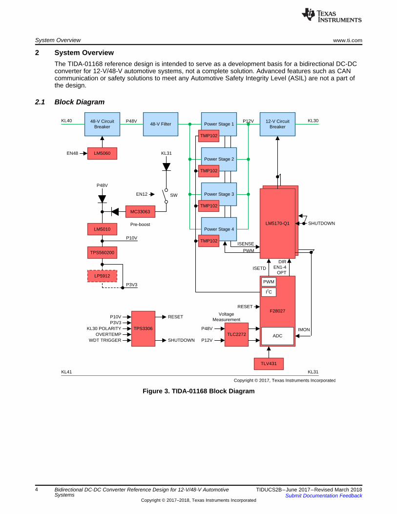
2 System OverviewThe TIDA-01168 reference design is intended to serve as a development basis for a bidirectional DC-DCconverter for 12-V/48-V automotive systems, not a complete solution. Advanced features such as CANcommunication or safety solutions to meet any Automotive Safety Integrity Level (ASIL) are not a part ofthe design.
2.1 Block Diagram
Figure 3. TIDA-01168 Block Diagram
KL41
Passenger Safety
Driver Assistance
Brake System
Engine Management
Transmission Control
Infotainment
...
Air Conditioning
Cooling Fan
Electric Heating
Water Pump
Fuel Pump
EPS
...
Screens Heating Roll Stabilization
Inverter
Bidirectional Current Flow
M / G Mechanical Coupling to ICE
KL31
3P
KL31KL41
DC / DCKL40 KL30
12 V 48 V
Copyright © 2017, Texas Instruments Incorporated
www.ti.com System Overview
5TIDUCS2B–June 2017–Revised March 2018Submit Documentation Feedback
Copyright © 2017–2018, Texas Instruments Incorporated
Bidirectional DC-DC Converter Reference Design for 12-V/48-V AutomotiveSystems
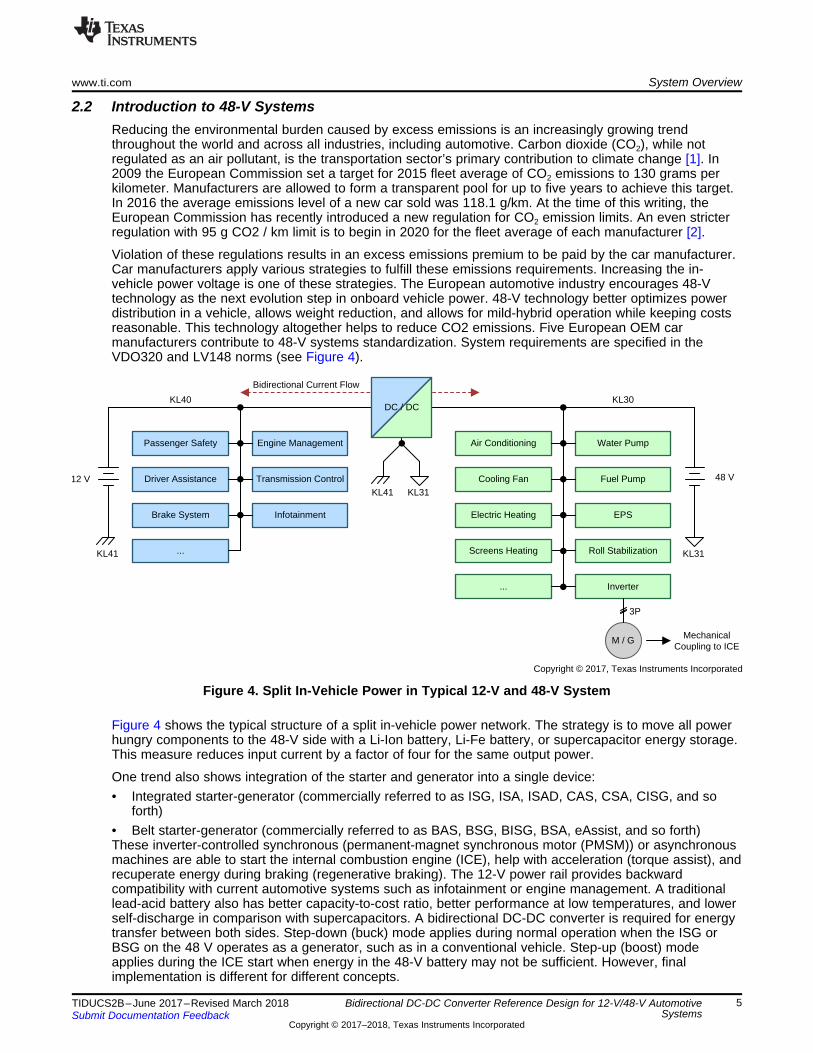
2.2 Introduction to 48-V SystemsReducing the environmental burden caused by excess emissions is an increasingly growing trendthroughout the world and across all industries, including automotive. Carbon dioxide (CO2), while notregulated as an air pollutant, is the transportation sector’s primary contribution to climate change [1]. In2009 the European Commission set a target for 2015 fleet average of CO2 emissions to 130 grams perkilometer. Manufacturers are allowed to form a transparent pool for up to five years to achieve this target.In 2016 the average emissions level of a new car sold was 118.1 g/km. At the time of this writing, theEuropean Commission has recently introduced a new regulation for CO2 emission limits. An even stricterregulation with 95 g CO2 / km limit is to begin in 2020 for the fleet average of each manufacturer [2].
Violation of these regulations results in an excess emissions premium to be paid by the car manufacturer.Car manufacturers apply various strategies to fulfill these emissions requirements. Increasing the in-vehicle power voltage is one of these strategies. The European automotive industry encourages 48-Vtechnology as the next evolution step in onboard vehicle power. 48-V technology better optimizes powerdistribution in a vehicle, allows weight reduction, and allows for mild-hybrid operation while keeping costsreasonable. This technology altogether helps to reduce CO2 emissions. Five European OEM carmanufacturers contribute to 48-V systems standardization. System requirements are specified in theVDO320 and LV148 norms (see Figure 4).
Figure 4. Split In-Vehicle Power in Typical 12-V and 48-V System
Figure 4 shows the typical structure of a split in-vehicle power network. The strategy is to move all powerhungry components to the 48-V side with a Li-Ion battery, Li-Fe battery, or supercapacitor energy storage.This measure reduces input current by a factor of four for the same output power.
One trend also shows integration of the starter and generator into a single device:• Integrated starter-generator (commercially referred to as ISG, ISA, ISAD, CAS, CSA, CISG, and so
forth)• Belt starter-generator (commercially referred to as BAS, BSG, BISG, BSA, eAssist, and so forth)These inverter-controlled synchronous (permanent-magnet synchronous motor (PMSM)) or asynchronousmachines are able to start the internal combustion engine (ICE), help with acceleration (torque assist), andrecuperate energy during braking (regenerative braking). The 12-V power rail provides backwardcompatibility with current automotive systems such as infotainment or engine management. A traditionallead-acid battery also has better capacity-to-cost ratio, better performance at low temperatures, and lowerself-discharge in comparison with supercapacitors. A bidirectional DC-DC converter is required for energytransfer between both sides. Step-down (buck) mode applies during normal operation when the ISG orBSG on the 48 V operates as a generator, such as in a conventional vehicle. Step-up (boost) modeapplies during the ICE start when energy in the 48-V battery may not be sufficient. However, finalimplementation is different for different concepts.
Shock Protection Range
Over Voltage Range
Higher Operating Range(Functional Restrictions Apply)
Operating Range(No Functional Restrictions)
Under Voltage Range
Lower Operating Range(Functional Restrictions Apply)
60 V (U48 shprotect)
54 V (U48 max, high, limited)
52 V (U48 max, unlimited)
48 V (U48n)
36 V (U48 min, unlimited)
24 V (U48 min, low, limited)
20 V (U48 stoprotect)
System Overview www.ti.com
6 TIDUCS2B–June 2017–Revised March 2018Submit Documentation Feedback
Copyright © 2017–2018, Texas Instruments Incorporated
Bidirectional DC-DC Converter Reference Design for 12-V/48-V AutomotiveSystems
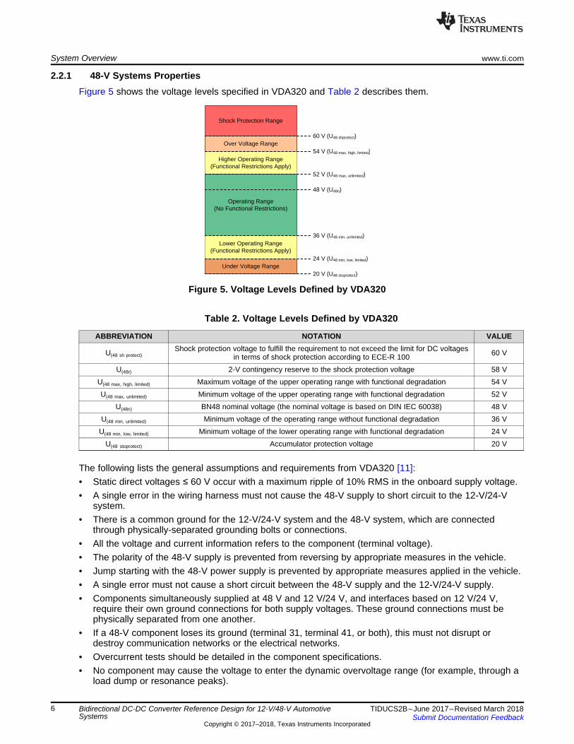
2.2.1 48-V Systems PropertiesFigure 5 shows the voltage levels specified in VDA320 and Table 2 describes them.
Figure 5. Voltage Levels Defined by VDA320
Table 2. Voltage Levels Defined by VDA320
ABBREVIATION NOTATION VALUE
U(48 sh protect)Shock protection voltage to fulfill the requirement to not exceed the limit for DC voltages
in terms of shock protection according to ECE-R 100 60 V
U(48r) 2-V contingency reserve to the shock protection voltage 58 VU(48 max, high, limited) Maximum voltage of the upper operating range with functional degradation 54 VU(48 max, unlimited) Minimum voltage of the upper operating range with functional degradation 52 V
U(48n) BN48 nominal voltage (the nominal voltage is based on DIN IEC 60038) 48 VU(48 min, unlimited) Minimum voltage of the operating range without functional degradation 36 V
U(48 min, low, limited) Minimum voltage of the lower operating range with functional degradation 24 VU(48 stoprotect) Accumulator protection voltage 20 V
The following lists the general assumptions and requirements from VDA320 [11]:• Static direct voltages ≤ 60 V occur with a maximum ripple of 10% RMS in the onboard supply voltage.• A single error in the wiring harness must not cause the 48-V supply to short circuit to the 12-V/24-V
system.• There is a common ground for the 12-V/24-V system and the 48-V system, which are connected
through physically-separated grounding bolts or connections.• All the voltage and current information refers to the component (terminal voltage).• The polarity of the 48-V supply is prevented from reversing by appropriate measures in the vehicle.• Jump starting with the 48-V power supply is prevented by appropriate measures applied in the vehicle.• A single error must not cause a short circuit between the 48-V supply and the 12-V/24-V supply.• Components simultaneously supplied at 48 V and 12 V/24 V, and interfaces based on 12 V/24 V,
require their own ground connections for both supply voltages. These ground connections must bephysically separated from one another.
• If a 48-V component loses its ground (terminal 31, terminal 41, or both), this must not disrupt ordestroy communication networks or the electrical networks.
• Overcurrent tests should be detailed in the component specifications.• No component may cause the voltage to enter the dynamic overvoltage range (for example, through a
load dump or resonance peaks).
C48 C12
KL31KL41
PWM
PWM
KL40 KL30
Q1
Q2
L
www.ti.com System Overview
7TIDUCS2B–June 2017–Revised March 2018Submit Documentation Feedback
Copyright © 2017–2018, Texas Instruments Incorporated
Bidirectional DC-DC Converter Reference Design for 12-V/48-V AutomotiveSystems
• If the voltage enters the overvoltage range up to U(48r) , countermeasures should be taken through thecomponent that is feeding energy back in or causing entry into the overvoltage range, so that thevoltage exits the overvoltage range at the lower boundary.
• If the voltage enters the lower limited function range, countermeasures should be taken so that thevoltage returns to the unlimited operation range.
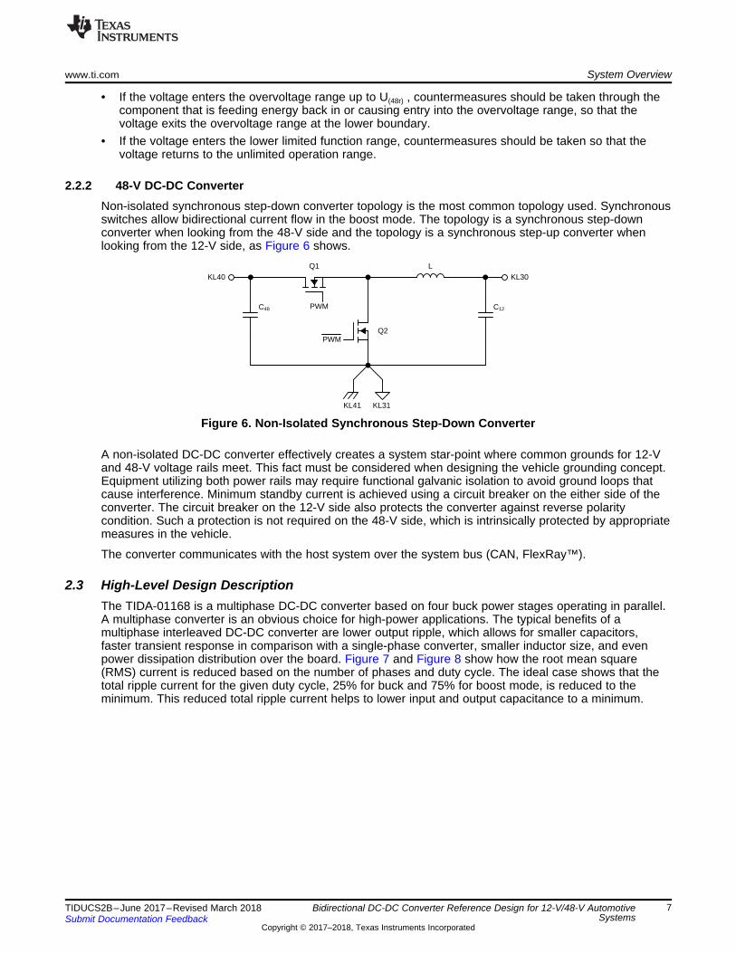
2.2.2 48-V DC-DC ConverterNon-isolated synchronous step-down converter topology is the most common topology used. Synchronousswitches allow bidirectional current flow in the boost mode. The topology is a synchronous step-downconverter when looking from the 48-V side and the topology is a synchronous step-up converter whenlooking from the 12-V side, as Figure 6 shows.
Figure 6. Non-Isolated Synchronous Step-Down Converter
A non-isolated DC-DC converter effectively creates a system star-point where common grounds for 12-Vand 48-V voltage rails meet. This fact must be considered when designing the vehicle grounding concept.Equipment utilizing both power rails may require functional galvanic isolation to avoid ground loops thatcause interference. Minimum standby current is achieved using a circuit breaker on the either side of theconverter. The circuit breaker on the 12-V side also protects the converter against reverse polaritycondition. Such a protection is not required on the 48-V side, which is intrinsically protected by appropriatemeasures in the vehicle.
The converter communicates with the host system over the system bus (CAN, FlexRay™).
2.3 High-Level Design DescriptionThe TIDA-01168 is a multiphase DC-DC converter based on four buck power stages operating in parallel.A multiphase converter is an obvious choice for high-power applications. The typical benefits of amultiphase interleaved DC-DC converter are lower output ripple, which allows for smaller capacitors,faster transient response in comparison with a single-phase converter, smaller inductor size, and evenpower dissipation distribution over the board. Figure 7 and Figure 8 show how the root mean square(RMS) current is reduced based on the number of phases and duty cycle. The ideal case shows that thetotal ripple current for the given duty cycle, 25% for buck and 75% for boost mode, is reduced to theminimum. This reduced total ripple current helps to lower input and output capacitance to a minimum.
KL40 KL30Rsense
KL41
½ LM5170-Q1
C2000
EN
DIR
ISE
TD
C2000
IMO
N
KL31
Copyright © 2017, Texas Instruments Incorporated
Duty Cycle
Nor
mal
ized
Rip
ple
Cur
rent
0 20% 40% 60% 80% 100%0.0
0.2
0.4
0.6
0.8
1.0
D008
1-phase2-phase3-phase
Duty Cycle
Nor
mal
ized
Rip
ple
Cur
rent
0 20% 40% 60% 80% 100%0.0
0.1
0.2
0.3
0.4
0.5
D009
1-phase2-phase3-phase
System Overview www.ti.com
8 TIDUCS2B–June 2017–Revised March 2018Submit Documentation Feedback
Copyright © 2017–2018, Texas Instruments Incorporated
Bidirectional DC-DC Converter Reference Design for 12-V/48-V AutomotiveSystems
Figure 7. Buck Output RMS Current, Boost InputRMS Current
Figure 8. Buck Input RMS Current, Boost OutputRMS Current
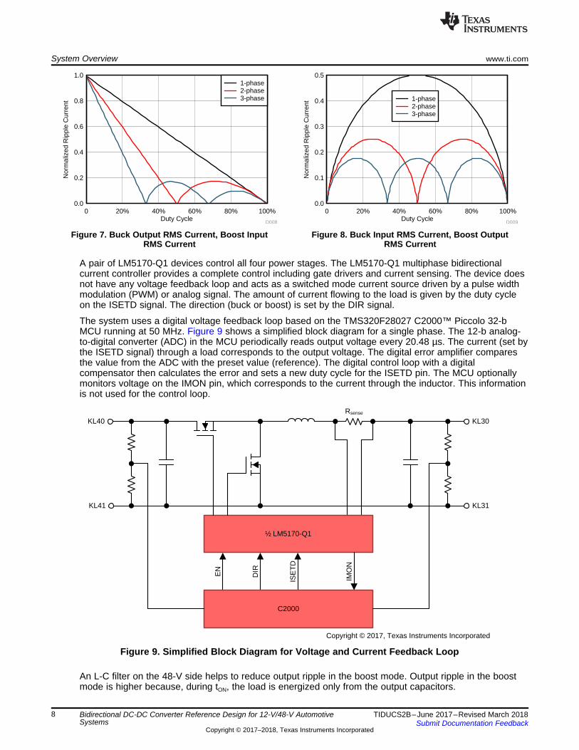
A pair of LM5170-Q1 devices control all four power stages. The LM5170-Q1 multiphase bidirectionalcurrent controller provides a complete control including gate drivers and current sensing. The device doesnot have any voltage feedback loop and acts as a switched mode current source driven by a pulse widthmodulation (PWM) or analog signal. The amount of current flowing to the load is given by the duty cycleon the ISETD signal. The direction (buck or boost) is set by the DIR signal.
The system uses a digital voltage feedback loop based on the TMS320F28027 C2000™ Piccolo 32-bMCU running at 50 MHz. Figure 9 shows a simplified block diagram for a single phase. The 12-b analog-to-digital converter (ADC) in the MCU periodically reads output voltage every 20.48 µs. The current (set bythe ISETD signal) through a load corresponds to the output voltage. The digital error amplifier comparesthe value from the ADC with the preset value (reference). The digital control loop with a digitalcompensator then calculates the error and sets a new duty cycle for the ISETD pin. The MCU optionallymonitors voltage on the IMON pin, which corresponds to the current through the inductor. This informationis not used for the control loop.
Figure 9. Simplified Block Diagram for Voltage and Current Feedback Loop
An L-C filter on the 48-V side helps to reduce output ripple in the boost mode. Output ripple in the boostmode is higher because, during tON, the load is energized only from the output capacitors.

www.ti.com System Overview
9TIDUCS2B–June 2017–Revised March 2018Submit Documentation Feedback
Copyright © 2017–2018, Texas Instruments Incorporated
Bidirectional DC-DC Converter Reference Design for 12-V/48-V AutomotiveSystems
Each side of the converter can be disconnected from the respective power rail by a circuit breaker basedon back-to-back N-MOSFETs configuration. The circuit breaker on the 12-V side is fully controlled by theLM5170-Q1 device, which protects against reverse polarity conditions and allows very low standby current(IQ) when the system is off. The circuit breaker is shut off when the LM5170-Q1 device detects a failure.This condition is reported by the nFAULT pin. The LM5060-Q1 high-side protection controller controls the48-V side circuit breaker. Although reverse polarity protection is usually not required for the 48-V rail, aback-to-back N-MOSFETs configuration is used to prevent any current flow when the system is off. TheLM5060-Q1 device can trigger on undervoltage, overvoltage, and overcurrent events.
The system can be turned on from either a 12-V or 48-V power rail. A pre-boost DC-DC converter basedon the MC33063A-Q1 device is used in the case of a turnon from the 12-V side triggered by the EN12signal. Input for this pre-boost circuit bypasses the high-current 12-V circuit breaker. Output of the pre-boost DC-DC converter is set to approximately 28 V to provide enough gate voltage for the 12-V circuitbreaker. The pre-boost DC-DC uses a hysteretic-based control scheme and therefore automatically stopsswitching when the 48-V is present. Standby current consumption can be further reduced by setting theEN12 signal low when the P48V voltage is present.
Two additional DC-DC converters are required for a bias power supply. The LM5010-Q1 is a high VIN step-down converter with a 10-V output for biasing LM5170-Q1 devices. The TPS560200-Q1 device is used forenergizing the rest of the circuitry. The 3.3-V output matches the digital-logic operating-voltage level. Anoptional linear post-regulator LP5912-Q1 can be used in case the switching noise influences the analogcircuitry.
A simple diagnostics block is available in the design. Four configurable TMP102-Q1 temperature sensorscommunicating over the I2C bus monitor the temperature for each power stage. The ALERT output signalsof these temperature sensors are connected to the shutdown signal, which switches off all the powerstages after reaching the overtemperature threshold. The TPS3306-Q1 voltage supervisor and watchdogmonitors the MCU and voltage rails. The programmable function input (PFI) detects polarity on KL30.Such a feature is required to restrict the 12-V circuit breaker opening during reverse polarity on the KL30.Without this restriction, high current flows through the inductor and body diode of the bottom MOSFET inall power stages, which results in permanent damage.
Plating
Base Copper
Prepreg 7628
Internal Copper
Core
Prepreg 7628
Internal Copper
Prepreg 7628
Prepreg 7628
Base Copper
Plating
25 m
70 m
180 m
180 m
35 m
710 m
35 m
180 m
180 m
70 m
25 m
Thermally Conductive
Insulation
PCB
PCB Traces
SK42 Heatsink
M3 Screw Insulating Bush
Bus-bars
System Overview www.ti.com
10 TIDUCS2B–June 2017–Revised March 2018Submit Documentation Feedback
Copyright © 2017–2018, Texas Instruments Incorporated
Bidirectional DC-DC Converter Reference Design for 12-V/48-V AutomotiveSystems
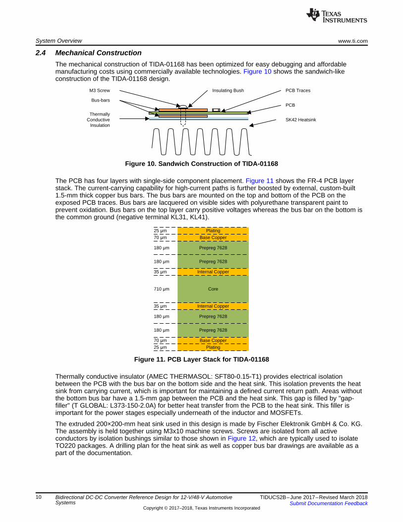
2.4 Mechanical ConstructionThe mechanical construction of TIDA-01168 has been optimized for easy debugging and affordablemanufacturing costs using commercially available technologies. Figure 10 shows the sandwich-likeconstruction of the TIDA-01168 design.
Figure 10. Sandwich Construction of TIDA-01168
The PCB has four layers with single-side component placement. Figure 11 shows the FR-4 PCB layerstack. The current-carrying capability for high-current paths is further boosted by external, custom-built1.5-mm thick copper bus bars. The bus bars are mounted on the top and bottom of the PCB on theexposed PCB traces. Bus bars are lacquered on visible sides with polyurethane transparent paint toprevent oxidation. Bus bars on the top layer carry positive voltages whereas the bus bar on the bottom isthe common ground (negative terminal KL31, KL41).
Figure 11. PCB Layer Stack for TIDA-01168
Thermally conductive insulator (AMEC THERMASOL: SFT80-0.15-T1) provides electrical isolationbetween the PCB with the bus bar on the bottom side and the heat sink. This isolation prevents the heatsink from carrying current, which is important for maintaining a defined current return path. Areas withoutthe bottom bus bar have a 1.5-mm gap between the PCB and the heat sink. This gap is filled by "gap-filler" (T GLOBAL: L373-150-2.0A) for better heat transfer from the PCB to the heat sink. This filler isimportant for the power stages especially underneath of the inductor and MOSFETs.
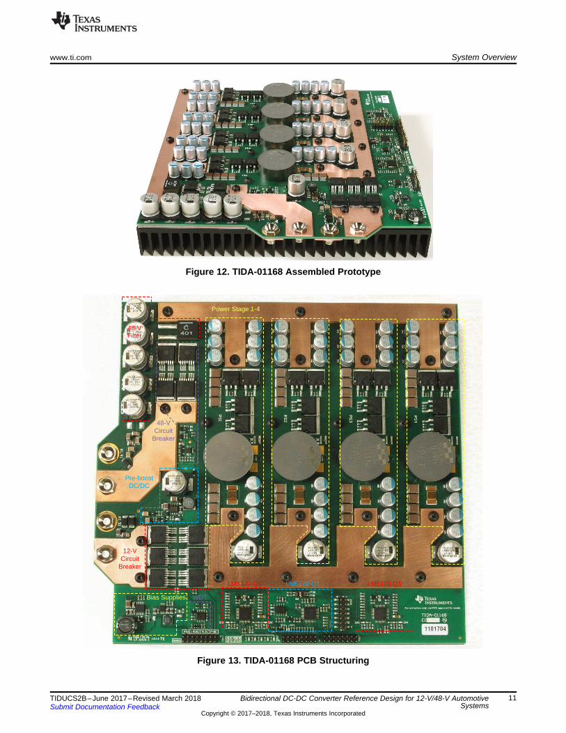
The extruded 200×200-mm heat sink used in this design is made by Fischer Elektronik GmbH & Co. KG.The assembly is held together using M3x10 machine screws. Screws are isolated from all activeconductors by isolation bushings similar to those shown in Figure 12, which are typically used to isolateTO220 packages. A drilling plan for the heat sink as well as copper bus bar drawings are available as apart of the documentation.
Power Stage 1-4
LM5170-Q1LM5170-Q1LM5170-Q1
WDTBias Supplies
12-VCircuit
Breaker
Pre-boostDC/DC
48-V Circuit
Breaker
48-V Filter
www.ti.com System Overview
11TIDUCS2B–June 2017–Revised March 2018Submit Documentation Feedback
Copyright © 2017–2018, Texas Instruments Incorporated
Bidirectional DC-DC Converter Reference Design for 12-V/48-V AutomotiveSystems
Figure 12. TIDA-01168 Assembled Prototype
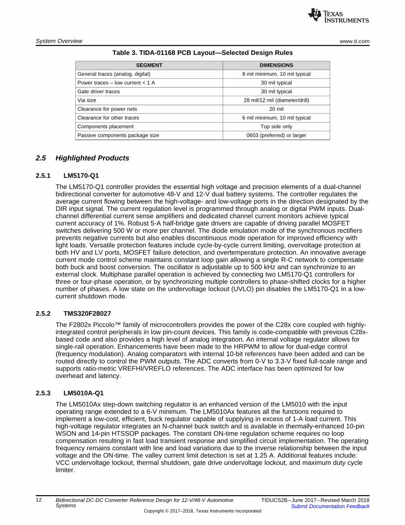
Figure 13. TIDA-01168 PCB Structuring
System Overview www.ti.com
12 TIDUCS2B–June 2017–Revised March 2018Submit Documentation Feedback
Copyright © 2017–2018, Texas Instruments Incorporated
Bidirectional DC-DC Converter Reference Design for 12-V/48-V AutomotiveSystems
Table 3. TIDA-01168 PCB Layout—Selected Design Rules
SEGMENT DIMENSIONSGeneral traces (analog, digital) 8 mil minimum, 10 mil typicalPower traces – low current < 1 A 30 mil typicalGate driver traces 30 mil typicalVia size 28 mil/12 mil (diameter/drill)Clearance for power nets 20 milClearance for other traces 6 mil minimum, 10 mil typicalComponents placement Top side onlyPassive components package size 0603 (preferred) or larger
2.5 Highlighted Products
2.5.1 LM5170-Q1The LM5170-Q1 controller provides the essential high voltage and precision elements of a dual-channelbidirectional converter for automotive 48-V and 12-V dual battery systems. The controller regulates theaverage current flowing between the high-voltage- and low-voltage ports in the direction designated by theDIR input signal. The current regulation level is programmed through analog or digital PWM inputs. Dual-channel differential current sense amplifiers and dedicated channel current monitors achieve typicalcurrent accuracy of 1%. Robust 5-A half-bridge gate drivers are capable of driving parallel MOSFETswitches delivering 500 W or more per channel. The diode emulation mode of the synchronous rectifiersprevents negative currents but also enables discontinuous mode operation for improved efficiency withlight loads. Versatile protection features include cycle-by-cycle current limiting, overvoltage protection atboth HV and LV ports, MOSFET failure detection, and overtemperature protection. An innovative averagecurrent mode control scheme maintains constant loop gain allowing a single R-C network to compensateboth buck and boost conversion. The oscillator is adjustable up to 500 kHz and can synchronize to anexternal clock. Multiphase parallel operation is achieved by connecting two LM5170-Q1 controllers forthree or four-phase operation, or by synchronizing multiple controllers to phase-shifted clocks for a highernumber of phases. A low state on the undervoltage lockout (UVLO) pin disables the LM5170-Q1 in a low-current shutdown mode.
2.5.2 TMS320F28027The F2802x Piccolo™ family of microcontrollers provides the power of the C28x core coupled with highly-integrated control peripherals in low pin-count devices. This family is code-compatible with previous C28x-based code and also provides a high level of analog integration. An internal voltage regulator allows forsingle-rail operation. Enhancements have been made to the HRPWM to allow for dual-edge control(frequency modulation). Analog comparators with internal 10-bit references have been added and can berouted directly to control the PWM outputs. The ADC converts from 0-V to 3.3-V fixed full-scale range andsupports ratio-metric VREFHI/VREFLO references. The ADC interface has been optimized for lowoverhead and latency.
2.5.3 LM5010A-Q1The LM5010Ax step-down switching regulator is an enhanced version of the LM5010 with the inputoperating range extended to a 6-V minimum. The LM5010Ax features all the functions required toimplement a low-cost, efficient, buck regulator capable of supplying in excess of 1-A load current. Thishigh-voltage regulator integrates an N-channel buck switch and is available in thermally-enhanced 10-pinWSON and 14-pin HTSSOP packages. The constant ON-time regulation scheme requires no loopcompensation resulting in fast load transient response and simplified circuit implementation. The operatingfrequency remains constant with line and load variations due to the inverse relationship between the inputvoltage and the ON-time. The valley current limit detection is set at 1.25 A. Additional features include:VCC undervoltage lockout, thermal shutdown, gate drive undervoltage lockout, and maximum duty cyclelimiter.
www.ti.com System Overview
13TIDUCS2B–June 2017–Revised March 2018Submit Documentation Feedback
Copyright © 2017–2018, Texas Instruments Incorporated
Bidirectional DC-DC Converter Reference Design for 12-V/48-V AutomotiveSystems
2.5.4 TPS560200-Q1The TPS560200-Q1 is a 17-V, 500-mA, low-IQ, adaptive ON-time D-CAP2 mode synchronous monolithicbuck converter with integrated MOSFETs in an easy-to-use 8-pin MSOP package. The TPS560200-Q1enables system designers to complete the suite of various end-equipment power bus regulators with acost-effective, low component count, and low standby current solution. The main control loop for thedevice uses the D-CAP2 mode control that provides a fast transient response with no externalcompensation components. The adaptive ON-time control supports seamless transition between PWMmode at higher load conditions and advanced Eco-mode™light load efficiency at light loads. TheTPS560200-Q1 also has a proprietary circuit that enables the device to adopt to both low equivalentseries resistance (ESR) output capacitors, such as POSCAP or SP-CAP, and ultra-low ESR ceramiccapacitors. The device operates from a 4.5-V to 17-V VIN input. The output voltage can be programmedbetween 0.8 V and 6.5 V. The device also features a fixed 2-ms soft-start time. The device is available inthe 8-pin MSOP package.
2.5.5 TMP102-Q1The TMP102-Q1 device is a digital temperature sensor ideal for NTC/PTC thermistor replacement wherehigh accuracy is required. The device offers an accuracy of ±0.5°C without requiring calibration or externalcomponent signal conditioning. Integrated circuit temperature sensors are highly linear and do not requirecomplex calculations or look-up tables to derive the temperature. The on-chip 12-bit ADC offersresolutions down to 0.0625°C. The 1.6-mm × 1.6-mm SOT563 package has a 68% smaller footprint thanan SOT23 package. The TMP102-Q1 device features SMBus™, which is compatible with two-wire and I2Cinterface and allows up to four devices on one bus. The device also features an SMBus alert function. Thedevice is specified to operate over supply voltages from 1.4 V to 3.6 V with the maximum quiescentcurrent of 10 µA over the full operating range. The TMP102-Q1 device is ideal for extended temperaturemeasurement in a variety of communication, computer, consumer, environmental, industrial, andinstrumentation applications. The device is specified for operation over a temperature range of –40°C to125°C. The TMP102-Q1 production units are 100% tested against sensors that are NIST-traceable andare verified with equipment that are NIST-traceable through ISO/IEC 17025 accredited calibrations.
2.5.6 TPS3306-Q1The TPS3306 family is a series of supervisory circuits designed for circuit initialization that requires twosupply voltages, primarily in digital signal processing (DSP) and processor-based systems. The productspectrum of the TPS3306-xx is designed for monitoring two independent supply voltages of 3.3 V/1.5 V,3.3 V/1.8 V, 3.3 V/2 V, 3.3 V/2.5 V, or 3.3 V/5 V. During power up, RESET is asserted when the supplyvoltage VDD becomes higher than 1.1 V. Thereafter, the supervisory circuits monitor the SENSEn inputsand keep RESET active as long as SENSEn remains below the threshold voltage VIT. An internal timerdelays the return of the RESET output to the inactive state (high) to ensure proper system reset. Thedelay time, td(typ) = 100 ms, starts after the SENSE1 and SENSE2 inputs have risen above the thresholdvoltage VIT. When the voltage at SENSE1 or SENSE2 input drops below the threshold voltage VIT, theoutput becomes active (low) again. The integrated power-fail (PFI) comparator with separate open-drain(PFO) output can be used for low-battery detection, power-fail warning, or for monitoring a power supplyother than the main supply. The TPS3306-xx devices integrate a watchdog timer that is periodicallytriggered by a positive or negative transition of WDI. When the supervising system fails to retrigger thewatchdog circuit within the time-out interval, tt(out) = 0.50 s, the RESET becomes active for the timeperiod td. This event also reinitializes the watchdog timer. Leaving WDI unconnected disables thewatchdog. The TPS3306-xx devices are available in standard 8-pin SO packages. The TPS3306-xxQfamily is characterized for operation over a temperature range of –40°C to 125°C.
2.5.7 MC33063A-Q1The MC33063A-Q1 device is an easy-to-use integrated circuit containing all the primary circuitry requiredfor building simple DC-DC converters. The device primarily consists of an internal temperature-compensated reference, a comparator, an oscillator, a PWM controller with active current limiting, a driver,and a high-current output switch. Thus, the device requires minimal external components to buildconverters in the boost, buck, and inverting topologies.

System Overview www.ti.com
14 TIDUCS2B–June 2017–Revised March 2018Submit Documentation Feedback
Copyright © 2017–2018, Texas Instruments Incorporated
Bidirectional DC-DC Converter Reference Design for 12-V/48-V AutomotiveSystems
2.5.8 TLC2272-Q1The TLC2272-Q1 and TLC2274-Q1 devices are dual and quadruple operational amplifiers from TexasInstruments. Both devices exhibit rail-to-rail output performance for increased dynamic range in single- orsplit-supply applications. The TLC227x-Q1 family offers 2 MHz of bandwidth and 3 V/µs of slew rate forhigher-speed applications. These devices offer comparable AC performance while having better noise,input offset voltage, and power dissipation than existing CMOS operational amplifiers. The TLC227x‑Q1has a noise voltage of 9 nV/√Hz, which is two times lower than competitive solutions. The TLC227x-Q1,exhibiting high input impedance and low noise, is excellent for small-signal conditioning for high-impedance sources, such as piezoelectric transducers. In addition, the rail-to-rail output feature, withsingle- or split-supplies, makes this family a great choice when interfacing with analog-to-digital converters(ADCs). For precision applications, the TLC227xA-Q1 family is available with a maximum input offsetvoltage of 950 µV. This family is fully characterized at 5 V and ±5 V. The devices offer increased outputdynamic range, lower noise voltage, and lower input offset voltage. This enhanced feature set allows thedevices to be used in a wider range of applications. For applications that require higher output drive andwider input voltage range, see the TLV2432-Q1 and TLV2442-Q1 devices. All of the parameters of theTLC227x-Q1 family enables the device to be applicable in most automotive applications.

www.ti.com Hardware Design
15TIDUCS2B–June 2017–Revised March 2018Submit Documentation Feedback
Copyright © 2017–2018, Texas Instruments Incorporated
Bidirectional DC-DC Converter Reference Design for 12-V/48-V AutomotiveSystems
3 Hardware Design
NOTE: This text does not cover the fundamental theory of operation.
3.1 48-V Circuit Breaker
3.1.1 DescriptionThe 48-V circuit breaker allows the DC-DC to completely disconnect from the 48-V battery rail using field-effect transistors (FETs). The block also protects the DC-DC against overvoltage and overcurrent. SeeTable 4 for a system interface overview.
Table 4. System Interface for 48-V Circuit Breaker
SIGNAL DIRECTION DESCRIPTIONKL40 In/Out 48-V car battery system terminal (positive)KL41 In/Out 48-V car battery system terminal (negative)P48V In/Out Protected 48-V rail (positive)PGND In/Out Protected 48-V rail (negative)
KL40_M Out 48-V battery four-wire voltage measurement terminal (positive)KL41_M Out 48-V battery four-wire voltage measurement terminal (negative)
EN48 In Enable signal.; voltage greater than 2.0 V enables the circuit breaker; voltage onthis pin shall not exceed 65 V
3.1.2 ConsiderationsThe 48-V circuit breaker conducts and disconnects current up to 50 A in both directions for voltages up to70 V. The limit of 70 V for 40 ms is given by the E48-02 Transient Overvoltage test defined in VDA320.The ability to disconnect current flow in both directions is generally required; therefore, a back-to-backMOSFETs configuration is used. This requirement is also beneficial; for example, pre-charging the 48-Vside capacitors to the KL40 voltage reduces the inrush current during turnon. Selected MOSFETs have avery low RDS(ON) and are rated up to 100 V. MOSFETs are in parallel to further reduce I2R losses causedby RDS(ON). Gate charge is not important as long as the LM5060-Q1 device is able to turn them ON andOFF fast enough. Give careful consideration to the safety operating area (SOA).
The protected side of the 48-V circuit breaker is used as a reference point for the voltage measurementcircuitry.
NOTE: The absolute maximum input and gate voltage for LM5060-Q1 is 75 V at 25°C. Contact a TIrepresentative for 100-V capable solutions.
KL40
KL41 PGND
P48V
EN5
VIN2
TIMER7
SEN1
GND6
UVLO4
OVP3
GATE10
OUT9
nPGD8
U100
LM5060Q1MMX/NOPB
EN
48
100kR100
100kR108
DNP2.70kR107
UVLO = 0 V
OVP = 76.07 V
0.01µFC107
0.047µFC108
0.01µFC106DNP
2.87kR103
Ilim = typ. 60 A
Soft-start
TP100
78V
D103SMAJ78CA
0
R109
KL41_M
KL40_M
0
R110 PGND
P48V
Kelvin connection, check the PCB layout
KL40 P48V
PGND
1.00kR101
1
4
2,3
,5,6
,7
Q100IPB180N10S402ATMA1
1
4
2,3
,5,6
,7
Q102IPB180N10S402ATMA1
1
4
2,3
,5,6
,7
Q101IPB180N10S402ATMA1
1
4
2,3
,5,6
,7
Q103IPB180N10S402ATMA1
78V
D1045.0SMDJ78ADNP
3
1
2
Q104MMBTA06-7-F
330kR106
D1001N4148W-7-F
2.00k
R105
20.5kR104
13
68VD105
1 3
68V
D101
PGNDD1021N4148W-7-F0.47µF
C100
0.47µFC103
10µFC101
10µFC102
10µFC104
10µFC105
Rdson = typ. 2mOhm
D106BAS516,115
D107BAS516,115
E1 to E2 Change in SCM. For E1 layout D106 takes place of formal R102 and D107 is hand-wired
Copyright © 2017, Texas Instruments Incorporated
Hardware Design www.ti.com
16 TIDUCS2B–June 2017–Revised March 2018Submit Documentation Feedback
Copyright © 2017–2018, Texas Instruments Incorporated
Bidirectional DC-DC Converter Reference Design for 12-V/48-V AutomotiveSystems
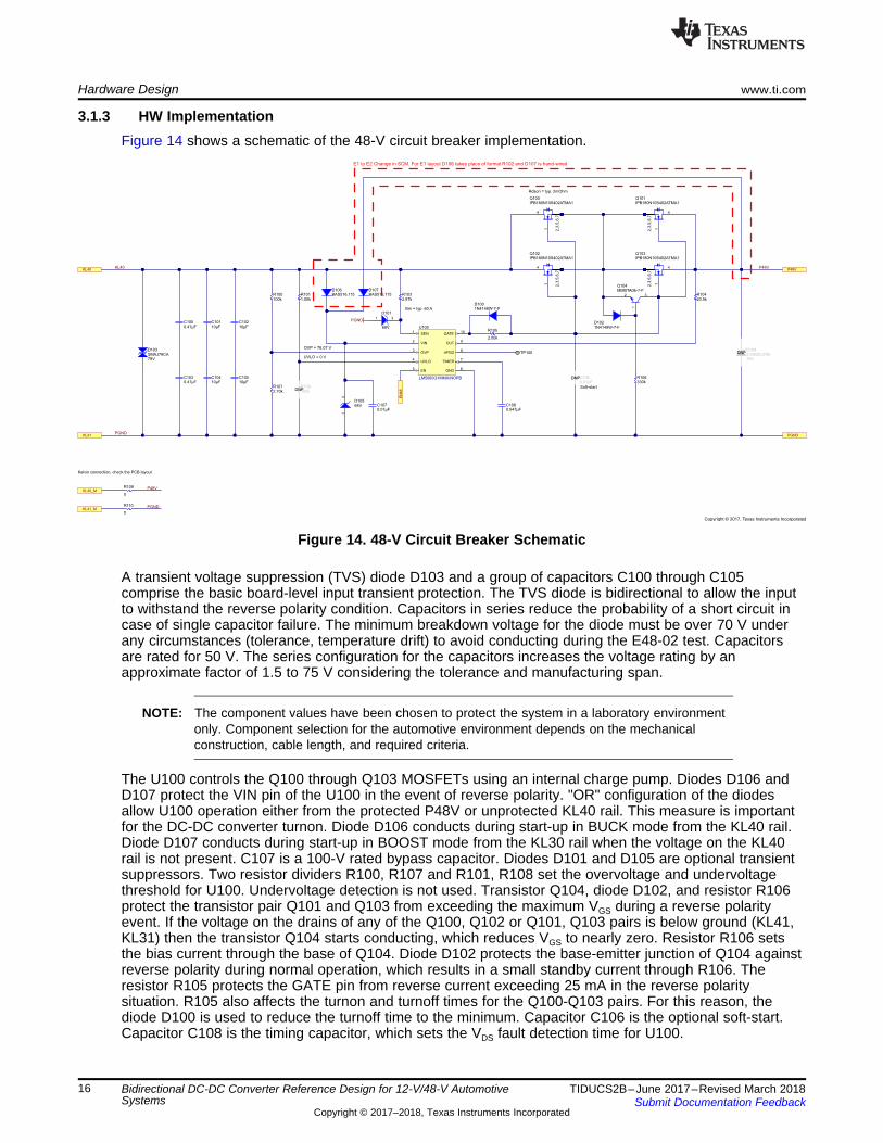
3.1.3 HW ImplementationFigure 14 shows a schematic of the 48-V circuit breaker implementation.
Figure 14. 48-V Circuit Breaker Schematic
A transient voltage suppression (TVS) diode D103 and a group of capacitors C100 through C105comprise the basic board-level input transient protection. The TVS diode is bidirectional to allow the inputto withstand the reverse polarity condition. Capacitors in series reduce the probability of a short circuit incase of single capacitor failure. The minimum breakdown voltage for the diode must be over 70 V underany circumstances (tolerance, temperature drift) to avoid conducting during the E48-02 test. Capacitorsare rated for 50 V. The series configuration for the capacitors increases the voltage rating by anapproximate factor of 1.5 to 75 V considering the tolerance and manufacturing span.
NOTE: The component values have been chosen to protect the system in a laboratory environmentonly. Component selection for the automotive environment depends on the mechanicalconstruction, cable length, and required criteria.
The U100 controls the Q100 through Q103 MOSFETs using an internal charge pump. Diodes D106 andD107 protect the VIN pin of the U100 in the event of reverse polarity. "OR" configuration of the diodesallow U100 operation either from the protected P48V or unprotected KL40 rail. This measure is importantfor the DC-DC converter turnon. Diode D106 conducts during start-up in BUCK mode from the KL40 rail.Diode D107 conducts during start-up in BOOST mode from the KL30 rail when the voltage on the KL40rail is not present. C107 is a 100-V rated bypass capacitor. Diodes D101 and D105 are optional transientsuppressors. Two resistor dividers R100, R107 and R101, R108 set the overvoltage and undervoltagethreshold for U100. Undervoltage detection is not used. Transistor Q104, diode D102, and resistor R106protect the transistor pair Q101 and Q103 from exceeding the maximum VGS during a reverse polarityevent. If the voltage on the drains of any of the Q100, Q102 or Q101, Q103 pairs is below ground (KL41,KL31) then the transistor Q104 starts conducting, which reduces VGS to nearly zero. Resistor R106 setsthe bias current through the base of Q104. Diode D102 protects the base-emitter junction of Q104 againstreverse polarity during normal operation, which results in a small standby current through R106. Theresistor R105 protects the GATE pin from reverse current exceeding 25 mA in the reverse polaritysituation. R105 also affects the turnon and turnoff times for the Q100-Q103 pairs. For this reason, thediode D100 is used to reduce the turnoff time to the minimum. Capacitor C106 is the optional soft-start.Capacitor C108 is the timing capacitor, which sets the VDS fault detection time for U100.
www.ti.com Hardware Design
17TIDUCS2B–June 2017–Revised March 2018Submit Documentation Feedback
Copyright © 2017–2018, Texas Instruments Incorporated
Bidirectional DC-DC Converter Reference Design for 12-V/48-V AutomotiveSystems
Resistors R109 and R110 allow disconnecting the voltage measurement circuitry from the measurementpoints during development and testing.
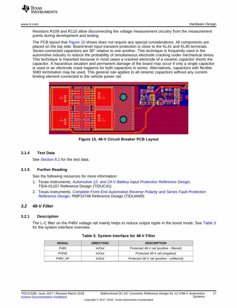
The PCB layout that Figure 15 shows does not require any special considerations. All components areplaced on the top side. Board-level input transient protection is close to the KL41 and KL40 terminals.Series-connected capacitors are 90° relative to one another. This technique is frequently used in theautomotive industry to reduce the probability of simultaneous electrode cracking under mechanical stress.This technique is important because in most cases a cracked electrode of a ceramic capacitor shorts thecapacitor. A hazardous situation and permanent damage of the board may occur if only a single capacitoris used or an electrode crack happens for both capacitors in series. Alternatively, capacitors with flexibleSMD termination may be used. This general rule applies to all ceramic capacitors without any current-limiting element connected to the vehicle power rail.
Figure 15. 48-V Circuit Breaker PCB Layout
3.1.4 Test DataSee Section 6.1 for the test data.
3.1.5 Further ReadingSee the following resources for more information:1. Texas Instruments, Automotive 12- and 24-V Battery Input Protection Reference Design,
TIDA-01167 Reference Design (TIDUC41)2. Texas Instruments, Complete Front End Automotive Reverse Polarity and Series Fault Protection
Reference Design, PMP10748 Reference Design (TIDUAW9)
3.2 48-V Filter
3.2.1 DescriptionThe L-C filter on the P48V voltage rail mainly helps to reduce output ripple in the boost mode. See Table 5for the system interface overview.
Table 5. System Interface for 48-V Filter
SIGNAL DIRECTION DESCRIPTIONP48V In/Out Protected 48-V rail (positive - filtered)PGND In/Out Protected 48-V rail (negative)
P48V_NF In/Out Protected 48-V rail (positive - unfiltered)
P48V
PGND
P48V_NF400nH
L200
150µFC204
150µFC203
150µFC202
150µFC201
PGND
150µFC200
400nH
L201
DNP
Option for higher current capabilities
Copyright © 2017, Texas Instruments Incorporated
Hardware Design www.ti.com
18 TIDUCS2B–June 2017–Revised March 2018Submit Documentation Feedback
Copyright © 2017–2018, Texas Instruments Incorporated
Bidirectional DC-DC Converter Reference Design for 12-V/48-V AutomotiveSystems
3.2.2 ConsiderationsIn contrast with a typical DC-DC converter application, a battery is connected to the output of a DC-DCconverter in 12-V/48-V automotive systems. This battery effectively helps to reduce output voltage ripple,especially within a low frequency range. Adding an L-C filter on the output of a boost converter helps toreduce output voltage ripple even further. Consider the following measures:• The highest output voltage ripple occurs in single-phase operation.• Output voltage ripple increases with a higher load.• Capacitors must be dimensioned for the given ripple current.• An L-C filter affects the compensation (stability) for both BUCK and BOOST mode.• The saturation current of the inductor must be higher than the average DC current.• Increasing the inductance for the same cutoff frequency results in a higher Q-factor and an additional
dumping network may be necessary to prevent oscillations and ringing.
NOTE: The SPICE circuit simulator helps with identifying initial component values. Use modelscontaining equivalent series inductance (ESL) and equivalent series resistance (ESR) forcapacitors and DC resistance (DCR) for inductors. A designer can replace the power stagewith an ideal current source that simulates the power inductor ripple current in continuousmode.
3.2.3 HW ImplementationFigure 16 shows a schematic of the 48-V filter implementation.
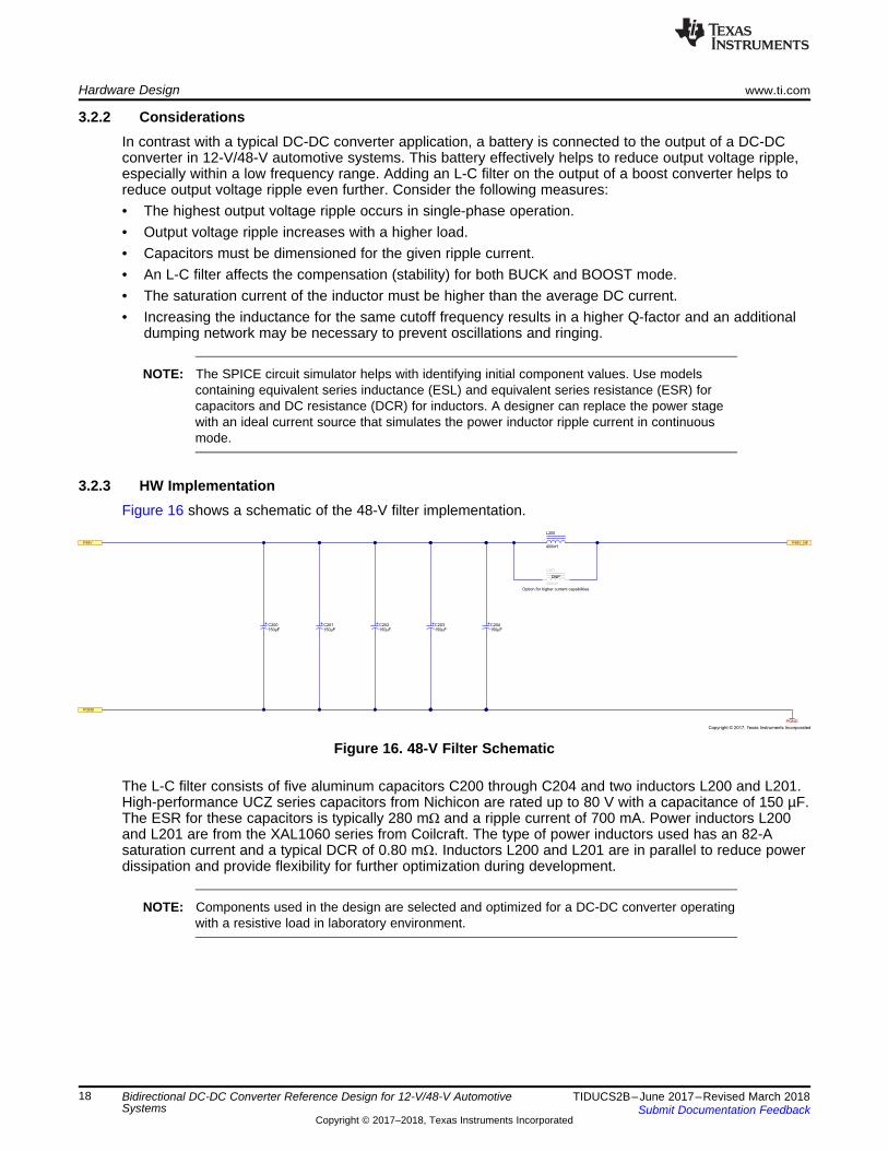
Figure 16. 48-V Filter Schematic
The L-C filter consists of five aluminum capacitors C200 through C204 and two inductors L200 and L201.High-performance UCZ series capacitors from Nichicon are rated up to 80 V with a capacitance of 150 µF.The ESR for these capacitors is typically 280 mΩ and a ripple current of 700 mA. Power inductors L200and L201 are from the XAL1060 series from Coilcraft. The type of power inductors used has an 82-Asaturation current and a typical DCR of 0.80 mΩ. Inductors L200 and L201 are in parallel to reduce powerdissipation and provide flexibility for further optimization during development.
NOTE: Components used in the design are selected and optimized for a DC-DC converter operatingwith a resistive load in laboratory environment.
www.ti.com Hardware Design
19TIDUCS2B–June 2017–Revised March 2018Submit Documentation Feedback
Copyright © 2017–2018, Texas Instruments Incorporated
Bidirectional DC-DC Converter Reference Design for 12-V/48-V AutomotiveSystems
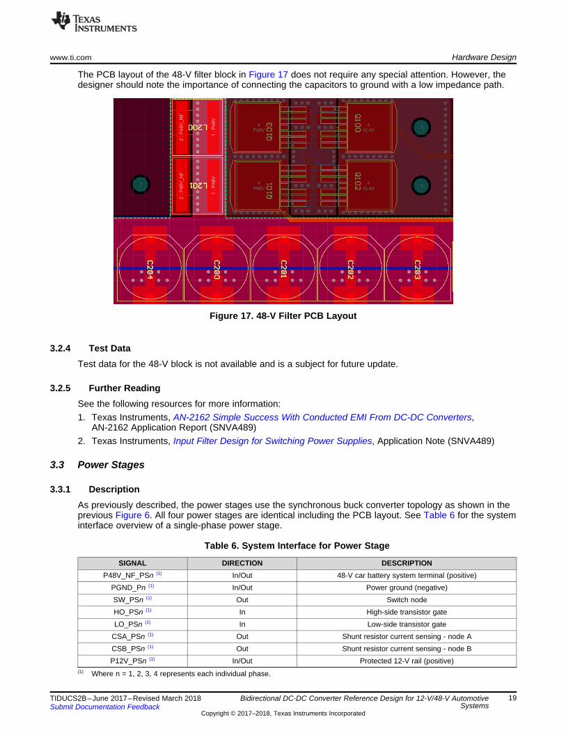
The PCB layout of the 48-V filter block in Figure 17 does not require any special attention. However, thedesigner should note the importance of connecting the capacitors to ground with a low impedance path.
Figure 17. 48-V Filter PCB Layout
3.2.4 Test DataTest data for the 48-V block is not available and is a subject for future update.
3.2.5 Further ReadingSee the following resources for more information:1. Texas Instruments, AN-2162 Simple Success With Conducted EMI From DC-DC Converters,
AN-2162 Application Report (SNVA489)2. Texas Instruments, Input Filter Design for Switching Power Supplies, Application Note (SNVA489)
3.3 Power Stages
3.3.1 DescriptionAs previously described, the power stages use the synchronous buck converter topology as shown in theprevious Figure 6. All four power stages are identical including the PCB layout. See Table 6 for the systeminterface overview of a single-phase power stage.
(1) Where n = 1, 2, 3, 4 represents each individual phase.
Table 6. System Interface for Power Stage
SIGNAL DIRECTION DESCRIPTIONP48V_NF_PSn (1) In/Out 48-V car battery system terminal (positive)
PGND_Pn (1) In/Out Power ground (negative)SW_PSn (1) Out Switch nodeHO_PSn (1) In High-side transistor gateLO_PSn (1) In Low-side transistor gate
CSA_PSn (1) Out Shunt resistor current sensing - node ACSB_PSn (1) Out Shunt resistor current sensing - node BP12V_PSn (1) In/Out Protected 12-V rail (positive)

P48V_NF
SW
HO
LO
CS
A
P12V
PGND
CS
B
1
34
Q300_PS1TK65G10N1,RQ
4.7µH
L300_PS1
51.0kR301_PS1
51.0kR304_PS1
51.0k
R308_PS1
51.0k
R309_PS1
1.00
R302_PS1
1.00
R305_PS1
1.00R306_PS1
1.00R307_PS1
10.0R303_PS1
DNP
Snubber
100pFC310_PS1DNP
39µFC313_PS1
39µFC314_PS1
39µFC315_PS1
39µFC312_PS1
39µFC311_PS1
39µFC300_PS1
4.7µFC301_PS1
4.7µFC302_PS1
4.7µFC303_PS1
4.7µFC304_PS1
39µFC318_PS1
39µFC319_PS1
4.7µFC305_PS1
4.7µFC306_PS1
4.7µFC307_PS1
4.7µFC308_PS1
39µFC316_PS1
39µFC317_PS1
180µFC309_PS1
PGND
1
34
Q301_PS1TK65G10N1,RQ
1
34
Q303_PS1TK65G10N1,RQ
1
34
Q302_PS1
PCV1J390MCL2GS withstands surge voltage of 72.4 V0.001R300_PS1
Copyright © 2017, Texas Instruments Incorporated
Hardware Design www.ti.com
20 TIDUCS2B–June 2017–Revised March 2018Submit Documentation Feedback
Copyright © 2017–2018, Texas Instruments Incorporated
Bidirectional DC-DC Converter Reference Design for 12-V/48-V AutomotiveSystems
3.3.2 ConsiderationsInput and output capacitor selection is affected by the bidirectional functionality. Capacitors swap theirfunction based on the operation mode. Increasing the output capacitance reduces output voltage rippleand output voltage overshoot during a load disconnect event. However, increased output capacitance alsohas a negative effect on transient response time and system costs. The selection of capacitors starts withchoosing the right capacitance and a sufficient ESR to fulfil the design requirements. The selectionprocess is then followed by choosing the other important parameters such as maximum ripple current,temperature range, and voltage rating.
NOTE: Calculating current sharing (for ripple current analysis) between capacitors with differentESR and capacitance in parallel is not trivial. The SPICE circuit simulator is the mostconvenient tool for the circuit analysis. The same capacitors in parallel can be replaced by asingle one. The total output capacitance is directly proportional and ESR is inverselyproportional to the number of the same capacitors in parallel.
Finding a proper inductor for energy storage is challenging. The DC current rating must correspond to themaximum output current (BUCK) with some extra margin for the inductor ripple current. The inductor mustnever saturate. Inductance is selected based on the switching frequency. Smaller inductance inductors inthe same package have a typically higher current rating due to a lower DCR, which results in a lower DCpower loss. However, lower inductance increases ripple current and output ripple.
MOSFET transistor selection varies based on the system requirements. MOSFET transistors in the powerstage negatively contribute to the total power dissipation, thus affecting the total system efficiency. Thepower dissipation results from conduction and switching losses. High-current MOSFET transistors with alow RDS(ON) minimize conduction losses (I2R), but typically have greater switching losses due to higher gatecharges and parasitics [1]. In an ideal case, the MOSFETs are selected in such a way that the sum ofconduction and switching losses is at the minimum. Various methods are available that detail how toselect the optimal MOSFETs for a DC-DC converter. See The J/K Method: A Technique to Select theOptimal MOSFET for an example using the J-K method.
A snubber circuit may be necessary for damping the parasitic inductances and capacitances on the switchnode during switching transitions.
A shunt resistor for current measurement must be rated to withstand the maximum ripple current throughthe inductor. Note the importance of using a shunt that has very low parasitic inductance and goodstability over the whole temperature range. See the section titled Compensating for the Non-Ideal CurrentSense Resistor in the LM5170-Q1 Multiphase Bidirectional Current Controller data sheet [2] to determinehow to compensate the parasitic inductance of the shunt resistor.
3.3.3 HW ImplementationFigure 18 shows a schematic of the power stage (single phase shown).
Figure 18. Power Stage Schematic (One Phase)
www.ti.com Hardware Design
21TIDUCS2B–June 2017–Revised March 2018Submit Documentation Feedback
Copyright © 2017–2018, Texas Instruments Incorporated
Bidirectional DC-DC Converter Reference Design for 12-V/48-V AutomotiveSystems
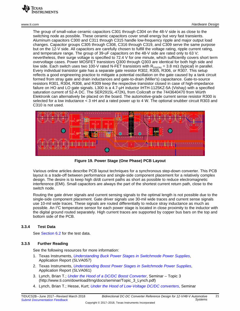
The group of small-value ceramic capacitors C301 through C304 on the 48-V side is as close to theswitching node as possible. These ceramic capacitors cover small energy but very fast transients.Aluminum capacitors C300 and C311 through C315 handle low-frequency ripple and major output loadchanges. Capacitor groups C305 through C308, C316 through C319, and C309 serve the same purposebut on the 12-V side. All capacitors are carefully chosen to fulfill the voltage rating, ripple current rating,and temperature range. The group of 39-uF capacitors on the 48-V side are rated only to 63 V;nevertheless, their surge voltage is specified to 72.4 V for one minute, which sufficiently covers short termovervoltage cases. Power MOSFET transistors Q300 through Q303 are identical for both high side andlow side. Each switch uses two 100-V rated N-FET transistors with RDS(ON) = 3.8 mΩ (typical) in parallel.Every individual transistor gate has a separate gate resistor R302, R305, R306, or R307. This setupreflects a good engineering practice to mitigate a potential oscillation on the gate caused by a tank circuitformed from stray gate and drain inductances and gate-to-drain (Miller's) capacitance. Gate-to-sourceresistors R301, R304, R308, and R309 keep the respective transistor closed in case of high-impedancefailure on HO and LO gate signals. L300 is a 4.7-µH inductor IHTH-1125KZ-5A (Vishay) with a specifiedsaturation current of 52-A DC. The SER2915L-472KL from Coilcraft or the 7443640470 from WürthElektronik can alternatively be placed on the board. The automotive-grade current sense resistor R300 isselected for a low inductance < 3 nH and a rated power up to 4 W. The optional snubber circuit R303 andC310 is not used.
Figure 19. Power Stage (One Phase) PCB Layout
Various online articles describe PCB layout techniques for a synchronous step-down converter. This PCBlayout is a trade-off between performance and single-side component placement for a relatively complexdesign. The desire is to keep high di/dt current paths as short as possible to reduce electromagneticinterference (EMI). Small capacitors are always the part of the shortest current return path, close to theswitch node.
Routing the gate driver signals and current sensing signals to the optimal length is not possible due to thesingle-side component placement. Gate driver signals use 30-mil wide traces and current sense signalsuse 10-mil wide traces. These signals are routed differentially to reduce stray inductance as much aspossible. An I2C temperature sensor for each power stage is located in close proximity to the inductor withthe digital ground routed separately. High current traces are supported by copper bus bars on the top andbottom side of the PCB.
3.3.4 Test DataSee Section 6.2 for the test data.
3.3.5 Further ReadingSee the following resources for more information:1. Texas Instruments, Understanding Buck Power Stages in Switchmode Power Supplies,
Application Report (SLVA057)2. Texas Instruments, Understanding Boost Power Stages in Switchmode Power Supplies,
Application Report (SLVA061)3. Lynch, Brian T.; Under the Hood of a DC/DC Boost Converter, Seminar – Topic 3
(http://www.ti.com/download/trng/docs/seminar/Topic_3_Lynch.pdf)4. Lynch, Brian T.; Hesse, Kurt; Under the Hood of Low-Voltage DC/DC converters, Seminar
Hardware Design www.ti.com
22 TIDUCS2B–June 2017–Revised March 2018Submit Documentation Feedback
Copyright © 2017–2018, Texas Instruments Incorporated
Bidirectional DC-DC Converter Reference Design for 12-V/48-V AutomotiveSystems
(http://application-notes.digchip.com/001/1-2958.pdf)5. Powerelectronics.com, Miller, James; The J/K Method: A Technique to Select the Optimal MOSFET,
Power Electronics Online Article (http://www.powerelectronics.com/dc-dc-converters/jk-method-technique-select-optimal-mosfet)
6. Texas Instruments, Taylor, Robert; Manack, Ryan; Controlling switch-node ringing in synchronousbuck converters, Power Management Technical Brief (SLYT465)
3.4 12-V Circuit Breaker
3.4.1 DescriptionThe 12-V circuit breaker protects the DC-DC converter against reverse polarity and allows disconnectingthe circuitry from the 12-V battery in case of a failure or to prevent current consumption when the systemis switched off. The functionality is the same as the 48-V circuit breaker except the 12-V circuit breakerhas a reverse polarity protection requirement. See Table 7 for a system interface overview.
Table 7. System Interface for 12-V Circuit Breaker
SIGNAL DIRECTION DESCRIPTIONKL30_BIAS Out Bias voltage rail for pre-boost circuitryKL30_POL Out Polarity detection for the 12-V battery
P12V In/Out Protected 12-V rail (positive)PGND In/Out Protected 12-V rail (negative)
EN12 In Enable signal; voltage greater than 2.0 V enables the circuitbreaker; optimized for 3.3-V/ 5-V logic signals
BRKG In Gate signal for the circuit breaker MOSFETsBRKS In Source signal for the circuit breaker MOSFETsKL30 In/Out 12-V car battery system terminal (positive)KL31 In/Out 12-V car battery system terminal (negative)
KL30_M Out 12-V battery four-wire voltage measurement terminal(positive)
KL31_M Out 12-V battery four-wire voltage measurement terminal(negative)
3.4.2 ConsiderationsThe DC-DC converter is disconnected from both power rails when the system is off. This setup ultimatelyrequires an external impulse to the system to initiate device start-up. This impulse can either be the EN12or EN48 signal. The circuit breaker on the 12-V side is controlled by the LM5170-Q1 controllers. Thecontrollers do not contain any internal charge pump for the circuit breaker MOSFET transistors. Voltageon the HV-port must be at least 10-V higher than on the LV-port (KL30) to allow these N-MOSFETtransistors to operate in the linear (ohmic) region as a switch. A back-to-back configuration of very lowRDS(ON) MOSFET transistors must be used similarly to the 48-V circuit breaker. A simple pre-boost circuit isconnected to the 12-V battery terminal (KL31) to bypass the 12-V circuit breaker and enable DC-DC start-up from the 12-V side.
Per industry expectations, the 12-V battery in a vehicle is user accessible. For this reason, a reversepolarity condition may occur. The system must detect this condition and force the 12-V circuit breaker offin case this situation arises. Opening the 12-V circuit breaker during a reverse polarity condition results inexcessive current flowing through the substrate diode of the low MOSFET and the inductor in the powerstage, which causes immediate damage of the system.
The protected side of the 12-V circuit breaker is used as a reference point for the voltage measurementcircuitry.
KL30
KL31
1
4
2,3
,5,6
,7
Q402AUIRFS8409-7P
P12V
PGND
0.47µFC401
KL30_BIAS
EN12
3
1
2
Q400
SI2319DS-T1-E3
3
1
2
Q401BC846B,215
PGND
10.0k
R402
10.0kR403
100kR400
15V
D401BZX384-C15,115
10.0kR401
D400
PMEG6010CEH,115
KL30_BIAS Reverse Polarity Protection
220kR404
68pFC404DNP
Optional Soft-Start
BRKG
BRKS
KL30_POL
RV400
V20P17AUTODNP
1
4
2,3
,5,6
,7
Q404AUIRFS8409-7P
1
4
2,3
,5,6
,7Q406AUIRFS8409-7P
1
4
2,3
,5,6
,7
Q403AUIRFS8409-7P
1
4
2,3
,5,6
,7
Q405AUIRFS8409-7P
1
4
2,3
,5,6
,7
Q407AUIRFS8409-7P
24V
D403SMBJ24A-13-F
28V
D402SMBJ28A-13-F
0.47µFC403
10µFC400
10µFC402
0
R405
KL31_M
KL30_M
0
R406 PGND
P12V
Kelvin connection, check the PCB layout
P12V
PGND
KL30
Copyright © 2017, Texas Instruments Incorporated
www.ti.com Hardware Design
23TIDUCS2B–June 2017–Revised March 2018Submit Documentation Feedback
Copyright © 2017–2018, Texas Instruments Incorporated
Bidirectional DC-DC Converter Reference Design for 12-V/48-V AutomotiveSystems
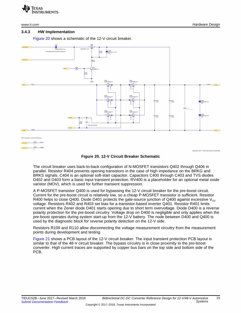
3.4.3 HW ImplementationFigure 20 shows a schematic of the 12-V circuit breaker.
Figure 20. 12-V Circuit Breaker Schematic
The circuit breaker uses back-to-back configuration of N-MOSFET transistors Q402 through Q406 inparallel. Resistor R404 prevents opening transistors in the case of high impedance on the BRKG andBRKS signals. C404 is an optional soft-start capacitor. Capacitors C400 through C403 and TVS diodesD402 and D403 form a basic input transient protection. RV400 is a placeholder for an optional metal oxidevaristor (MOV), which is used for further transient suppression.
A P-MOSFET transistor Q400 is used for bypassing the 12-V circuit breaker for the pre-boost circuit.Current for the pre-boost circuit is relatively low, so a cheap P-MOSFET transistor is sufficient. ResistorR400 helps to close Q400. Diode D401 protects the gate-source junction of Q400 against excessive VGSvoltage. Resistors R402 and R403 set bias for a transistor-based inverter Q401. Resistor R401 limitscurrent when the Zener diode D401 starts opening due to short term overvoltage. Diode D400 is a reversepolarity protection for the pre-boost circuitry. Voltage drop on D400 is negligible and only applies when thepre-boost operates during system start-up from the 12-V battery. The node between D400 and Q400 isused by the diagnostic block for reverse polarity detection on the 12-V side.
Resistors R109 and R110 allow disconnecting the voltage measurement circuitry from the measurementpoints during development and testing.
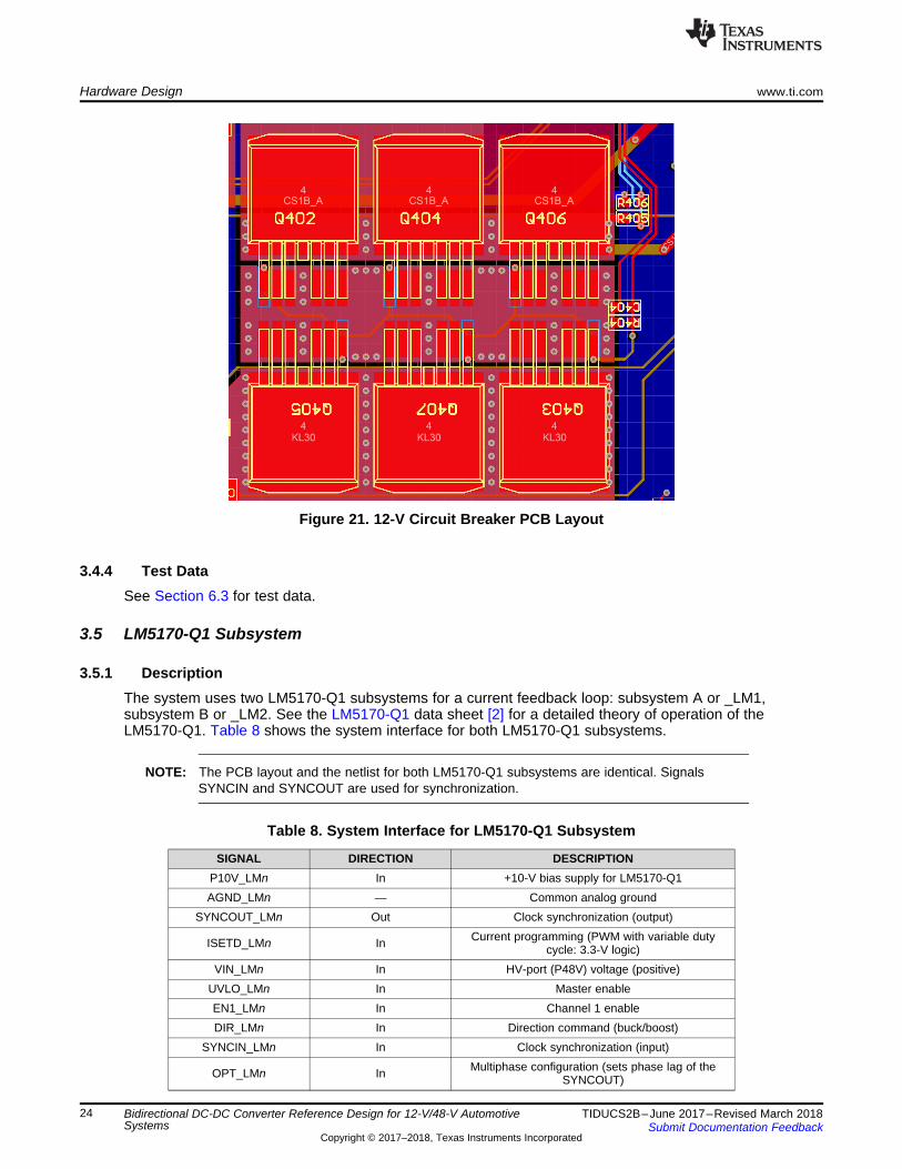
Figure 21 shows a PCB layout of the 12-V circuit breaker. The input transient protection PCB layout issimilar to that of the 48-V circuit breaker. The bypass circuitry is in close proximity to the pre-boostconverter. High current traces are supported by copper bus bars on the top side and bottom side of thePCB.
Hardware Design www.ti.com
24 TIDUCS2B–June 2017–Revised March 2018Submit Documentation Feedback
Copyright © 2017–2018, Texas Instruments Incorporated
Bidirectional DC-DC Converter Reference Design for 12-V/48-V AutomotiveSystems
Figure 21. 12-V Circuit Breaker PCB Layout
3.4.4 Test DataSee Section 6.3 for test data.
3.5 LM5170-Q1 Subsystem
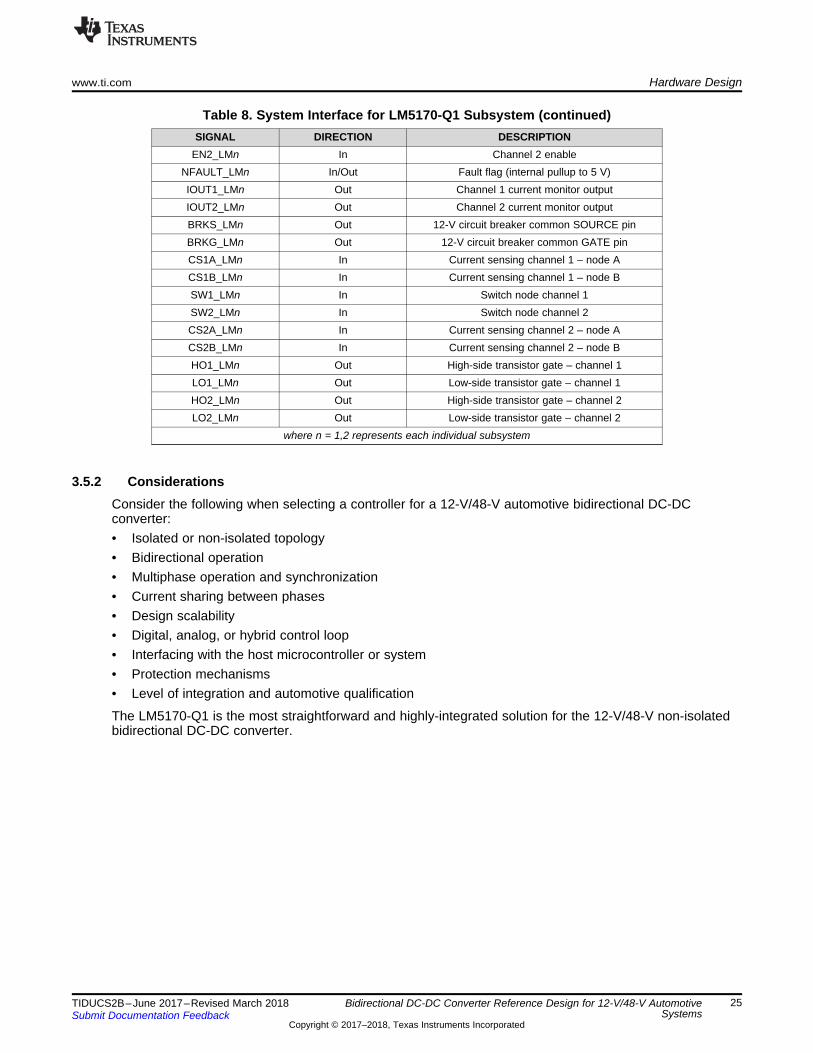
3.5.1 DescriptionThe system uses two LM5170-Q1 subsystems for a current feedback loop: subsystem A or _LM1,subsystem B or _LM2. See the LM5170-Q1 data sheet [2] for a detailed theory of operation of theLM5170-Q1. Table 8 shows the system interface for both LM5170-Q1 subsystems.
NOTE: The PCB layout and the netlist for both LM5170-Q1 subsystems are identical. SignalsSYNCIN and SYNCOUT are used for synchronization.
Table 8. System Interface for LM5170-Q1 Subsystem
SIGNAL DIRECTION DESCRIPTIONP10V_LMn In +10-V bias supply for LM5170-Q1AGND_LMn — Common analog ground
SYNCOUT_LMn Out Clock synchronization (output)
ISETD_LMn In Current programming (PWM with variable dutycycle: 3.3-V logic)
VIN_LMn In HV-port (P48V) voltage (positive)UVLO_LMn In Master enableEN1_LMn In Channel 1 enableDIR_LMn In Direction command (buck/boost)
SYNCIN_LMn In Clock synchronization (input)
OPT_LMn In Multiphase configuration (sets phase lag of theSYNCOUT)
www.ti.com Hardware Design
25TIDUCS2B–June 2017–Revised March 2018Submit Documentation Feedback
Copyright © 2017–2018, Texas Instruments Incorporated
Bidirectional DC-DC Converter Reference Design for 12-V/48-V AutomotiveSystems
Table 8. System Interface for LM5170-Q1 Subsystem (continued)SIGNAL DIRECTION DESCRIPTION
EN2_LMn In Channel 2 enableNFAULT_LMn In/Out Fault flag (internal pullup to 5 V)IOUT1_LMn Out Channel 1 current monitor outputIOUT2_LMn Out Channel 2 current monitor outputBRKS_LMn Out 12-V circuit breaker common SOURCE pinBRKG_LMn Out 12-V circuit breaker common GATE pinCS1A_LMn In Current sensing channel 1 – node ACS1B_LMn In Current sensing channel 1 – node BSW1_LMn In Switch node channel 1SW2_LMn In Switch node channel 2CS2A_LMn In Current sensing channel 2 – node ACS2B_LMn In Current sensing channel 2 – node BHO1_LMn Out High-side transistor gate – channel 1LO1_LMn Out Low-side transistor gate – channel 1HO2_LMn Out High-side transistor gate – channel 2LO2_LMn Out Low-side transistor gate – channel 2
where n = 1,2 represents each individual subsystem
3.5.2 ConsiderationsConsider the following when selecting a controller for a 12-V/48-V automotive bidirectional DC-DCconverter:• Isolated or non-isolated topology• Bidirectional operation• Multiphase operation and synchronization• Current sharing between phases• Design scalability• Digital, analog, or hybrid control loop• Interfacing with the host microcontroller or system• Protection mechanisms• Level of integration and automotive qualification
The LM5170-Q1 is the most straightforward and highly-integrated solution for the 12-V/48-V non-isolatedbidirectional DC-DC converter.
CS1A
CS1B
BRKS
BRKG
UV
LO
VIN
nFAULT
IOU
T2
IOU
T1
EN2
EN1
SYNCOUT
SYNCIN
ISETD
DIR
AGND
RAMP128
EN139
DIR44
ISETA45
ISETD42
SYNCIN40
SYNCOUT41
OSC47
RAMP28
AGND46
OPT29
EN243
HO215
SW213
HB214
LO217
FAULT27
IPK30
DT48
VCCA31
SS12
BRKG34
BRKS33
LO120
PGND18
VCC19
HB123
SW124
HO122
OV
PA
9
CS
A2
1
CS
B2
2
CO
MP
211
IOU
T2
38
OV
PB
25
DA
P49
VIN
6
UV
LO
10
VIN
X4
IOU
T1
37
CS
A1
36
CS
B1
35
CO
MP
12
6NC
3
NC5
NC7
NC16
NC21
NC32
U900_LM1LM5170QPHPRQ1
HO1
LO1
LO2
D900_LM1
PMEG6010CEH,1152.00
R907_LM1P10V
P10V
SW1
HO2
D901_LM1
PMEG6010CEH,1152.00
R913_LM1P10V
SW2
PGND
P10V24.0
R910_LM1
4.7µFC910_LM1
1µFC909_LM1
0.47µFC911_LM1
0.47µFC908_LM1
AGND
P10V
AGND
0.047µFC903_LM1
AGND
CS2A
CS2B
0.047µFC915_LM1
AGND
100pFC902_LM1DNP
100pFC904_LM1DNP
100pFC914_LM1DNP
100pFC916_LM1DNP
10.0
R914_LM1
10.0
R915_LM1
10.0
R901_LM1
10.0
R904_LM1
634R920_LM1
0.15µFC917_LM1
AGND
AGND
0.15µFC901_LM1
634R900_LM1
AGND
64.9kR918_LM1
AGND
100pFC918_LM1
AGND
100pFC919_LM1
48-V OVP Limit = 56.0 V 12-V OVP Limit = 19.4 V
64.9kR919_LM1
0.01µFC913_LM1
AGND
VIN
X
95.3kR902_LM1
AGND
95.3kR903_LM1
AGND
VINX
R(RAMP) = 9.6 / fsw * C(RAMP)
P10V
AGND
1µFC907_LM1
AGND
AGND
10.0kR908_LM1
AGND
10.0kR906_LM1
DNP
10.0kR905_LM1
AGND
P10V
OPT
SS = TBD
MOSFET test = OFF
3300pFC912_LM1
AGND
40.2kR909_LM1
AGND
AGND
fsw=99.5 kHz
40.2kR912_LM1
IPK = 48.2 A
Adaptive DT = VCC
ISETD Used
1000pFC900_LM1
1000pFC920_LM1
1000pFC905_LM1
1000pFC906_LM1
Yellow
21
D902_LM1
1.50kR916_LM1
AGND
EN1
EN2
EN1
Yellow
21
D903_LM1
AGND
EN2
Iled = 1mA
1.50kR917_LM1
10.0kR911_LM1
AGND
Termination
Copyright © 2017, Texas Instruments Incorporated
Hardware Design www.ti.com
26 TIDUCS2B–June 2017–Revised March 2018Submit Documentation Feedback
Copyright © 2017–2018, Texas Instruments Incorporated
Bidirectional DC-DC Converter Reference Design for 12-V/48-V AutomotiveSystems
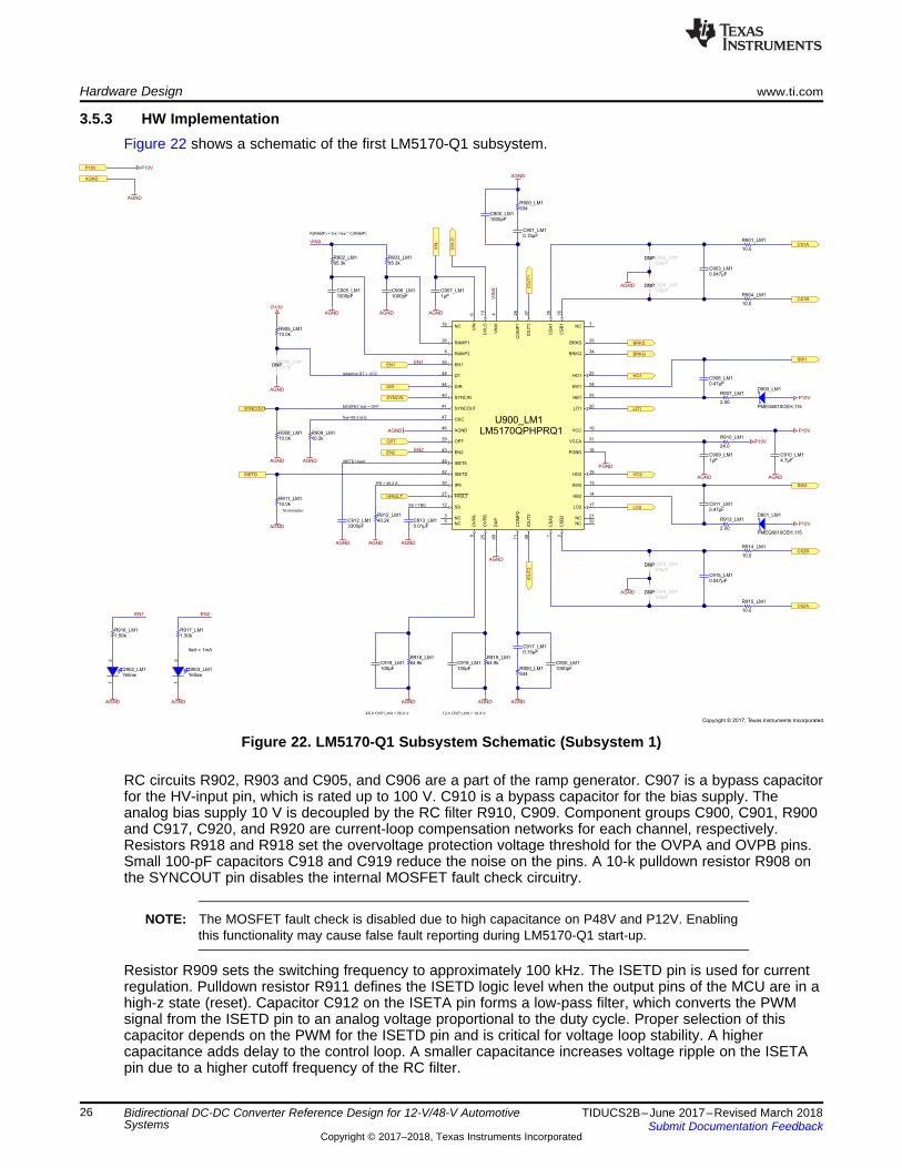
3.5.3 HW ImplementationFigure 22 shows a schematic of the first LM5170-Q1 subsystem.
Figure 22. LM5170-Q1 Subsystem Schematic (Subsystem 1)
RC circuits R902, R903 and C905, and C906 are a part of the ramp generator. C907 is a bypass capacitorfor the HV-input pin, which is rated up to 100 V. C910 is a bypass capacitor for the bias supply. Theanalog bias supply 10 V is decoupled by the RC filter R910, C909. Component groups C900, C901, R900and C917, C920, and R920 are current-loop compensation networks for each channel, respectively.Resistors R918 and R918 set the overvoltage protection voltage threshold for the OVPA and OVPB pins.Small 100-pF capacitors C918 and C919 reduce the noise on the pins. A 10-k pulldown resistor R908 onthe SYNCOUT pin disables the internal MOSFET fault check circuitry.
NOTE: The MOSFET fault check is disabled due to high capacitance on P48V and P12V. Enablingthis functionality may cause false fault reporting during LM5170-Q1 start-up.
Resistor R909 sets the switching frequency to approximately 100 kHz. The ISETD pin is used for currentregulation. Pulldown resistor R911 defines the ISETD logic level when the output pins of the MCU are in ahigh-z state (reset). Capacitor C912 on the ISETA pin forms a low-pass filter, which converts the PWMsignal from the ISETD pin to an analog voltage proportional to the duty cycle. Proper selection of thiscapacitor depends on the PWM for the ISETD pin and is critical for voltage loop stability. A highercapacitance adds delay to the control loop. A smaller capacitance increases voltage ripple on the ISETApin due to a higher cutoff frequency of the RC filter.
www.ti.com Hardware Design
27TIDUCS2B–June 2017–Revised March 2018Submit Documentation Feedback
Copyright © 2017–2018, Texas Instruments Incorporated
Bidirectional DC-DC Converter Reference Design for 12-V/48-V AutomotiveSystems
A 10-k pullup resistor R905 sets the internal adaptive dead-time control between the high-side and low-side driver. Resistor R906 is a placeholder for the fixed dead-time settings. Resistor R912 programs thethreshold for the cycle-by-cycle current limit comparator. Capacitor C913 defines soft-start time.
Component groups R901, R904, C903, C902, C904 and R914, R915, C915, C914, and C916 compensateparasitic inductance of the sense resistor. Components C908, R907, D900 and R911, R913, and R901are bootstrap circuits for high-side MOSFET drivers.
Channel activity is visualized by LEDs D902 and D903 connected to EN1 and EN2 signals. ResistorsR916 and R917 set the current through the LEDs to approximately 1 mA.
NOTE: Always refer to the latest revision of a data sheet for proper component selection. TheLM5170-Q1 data sheet contains detailed design procedure beginning in the section titledDesign Requirements [2].
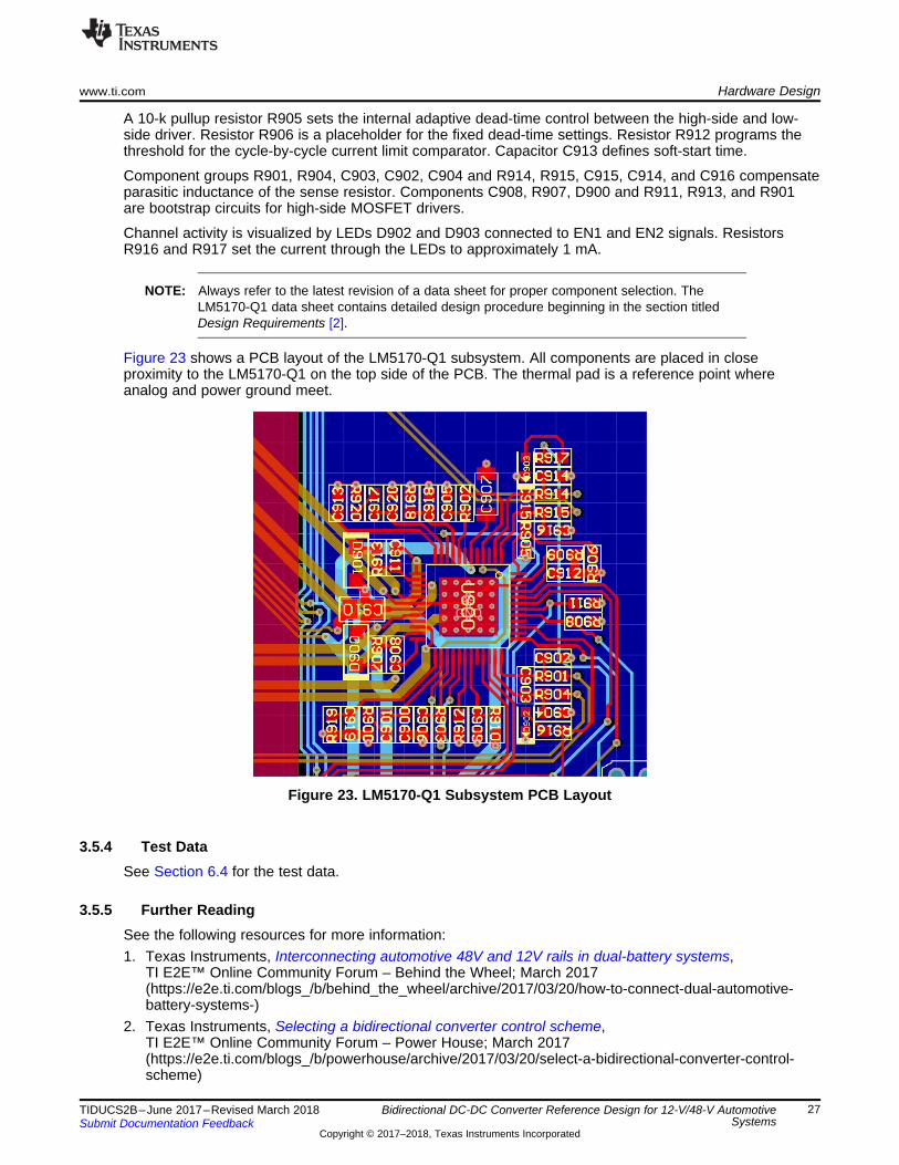
Figure 23 shows a PCB layout of the LM5170-Q1 subsystem. All components are placed in closeproximity to the LM5170-Q1 on the top side of the PCB. The thermal pad is a reference point whereanalog and power ground meet.
Figure 23. LM5170-Q1 Subsystem PCB Layout
3.5.4 Test DataSee Section 6.4 for the test data.
3.5.5 Further ReadingSee the following resources for more information:1. Texas Instruments, Interconnecting automotive 48V and 12V rails in dual-battery systems,
TI E2E™ Online Community Forum – Behind the Wheel; March 2017(https://e2e.ti.com/blogs_/b/behind_the_wheel/archive/2017/03/20/how-to-connect-dual-automotive-battery-systems-)
2. Texas Instruments, Selecting a bidirectional converter control scheme,TI E2E™ Online Community Forum – Power House; March 2017(https://e2e.ti.com/blogs_/b/powerhouse/archive/2017/03/20/select-a-bidirectional-converter-control-scheme)
Hardware Design www.ti.com
28 TIDUCS2B–June 2017–Revised March 2018Submit Documentation Feedback
Copyright © 2017–2018, Texas Instruments Incorporated
Bidirectional DC-DC Converter Reference Design for 12-V/48-V AutomotiveSystems
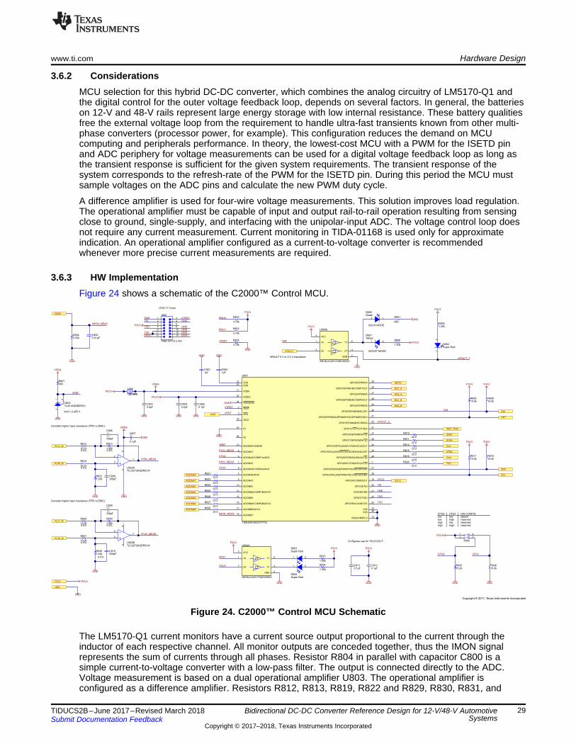
3.6 C2000™ MCU
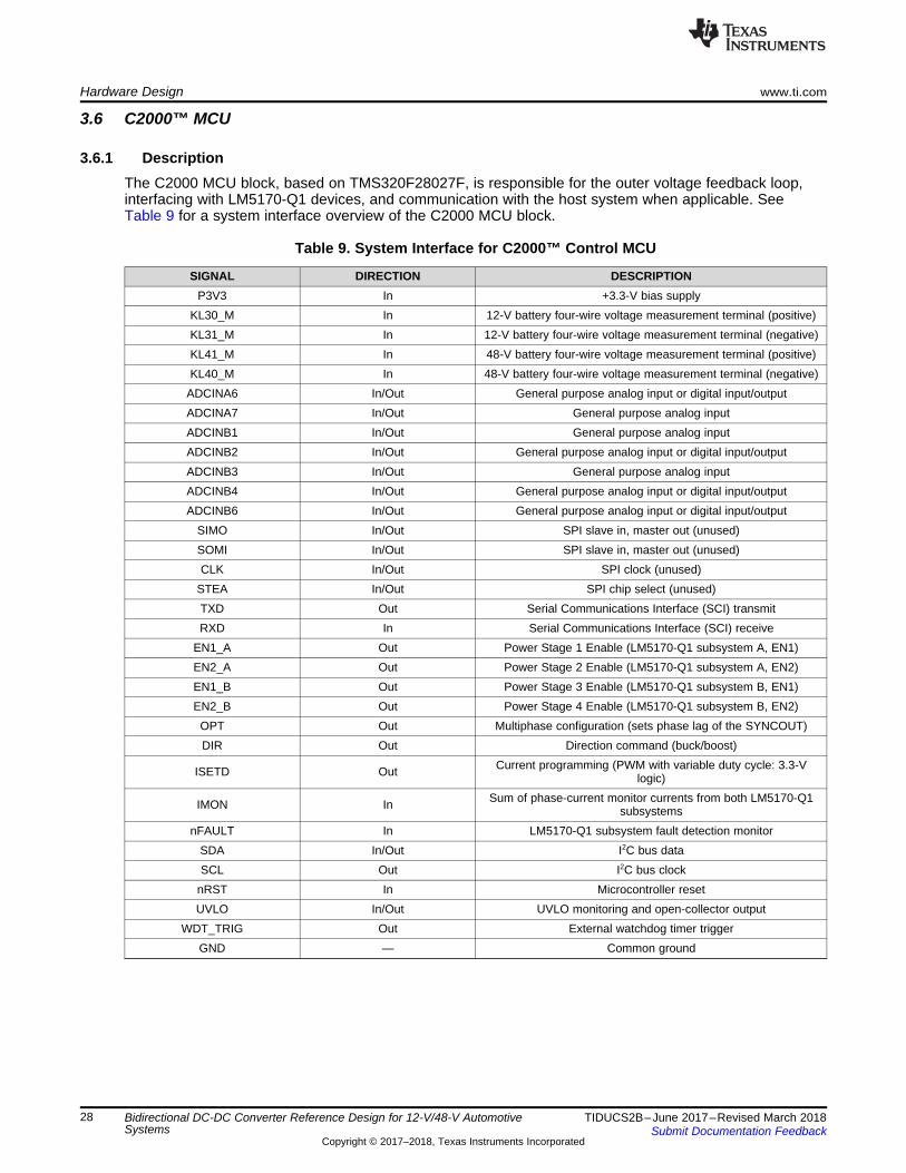
3.6.1 DescriptionThe C2000 MCU block, based on TMS320F28027F, is responsible for the outer voltage feedback loop,interfacing with LM5170-Q1 devices, and communication with the host system when applicable. SeeTable 9 for a system interface overview of the C2000 MCU block.
Table 9. System Interface for C2000™ Control MCU
SIGNAL DIRECTION DESCRIPTIONP3V3 In +3.3-V bias supply
KL30_M In 12-V battery four-wire voltage measurement terminal (positive)KL31_M In 12-V battery four-wire voltage measurement terminal (negative)KL41_M In 48-V battery four-wire voltage measurement terminal (positive)KL40_M In 48-V battery four-wire voltage measurement terminal (negative)
ADCINA6 In/Out General purpose analog input or digital input/outputADCINA7 In/Out General purpose analog inputADCINB1 In/Out General purpose analog inputADCINB2 In/Out General purpose analog input or digital input/outputADCINB3 In/Out General purpose analog inputADCINB4 In/Out General purpose analog input or digital input/outputADCINB6 In/Out General purpose analog input or digital input/output
SIMO In/Out SPI slave in, master out (unused)SOMI In/Out SPI slave in, master out (unused)CLK In/Out SPI clock (unused)
STEA In/Out SPI chip select (unused)TXD Out Serial Communications Interface (SCI) transmitRXD In Serial Communications Interface (SCI) receive
EN1_A Out Power Stage 1 Enable (LM5170-Q1 subsystem A, EN1)EN2_A Out Power Stage 2 Enable (LM5170-Q1 subsystem A, EN2)EN1_B Out Power Stage 3 Enable (LM5170-Q1 subsystem B, EN1)EN2_B Out Power Stage 4 Enable (LM5170-Q1 subsystem B, EN2)
OPT Out Multiphase configuration (sets phase lag of the SYNCOUT)DIR Out Direction command (buck/boost)
ISETD Out Current programming (PWM with variable duty cycle: 3.3-Vlogic)
IMON In Sum of phase-current monitor currents from both LM5170-Q1subsystems
nFAULT In LM5170-Q1 subsystem fault detection monitorSDA In/Out I2C bus dataSCL Out I2C bus clock
nRST In Microcontroller resetUVLO In/Out UVLO monitoring and open-collector output
WDT_TRIG Out External watchdog timer triggerGND — Common ground
ADCINA0/VREFHI10
ADCINA18
ADCINA2/COMP1A/AIO29
ADCINA37
ADCINA4/COMP2A/AIO45
ADCINA6/AIO64
ADCINA76
ADCINB113
ADCINB2/COMP1B/AIO1014
ADCINB315
ADCINB4/COMP2B/AIO1216
ADCINB6/AIO1417
ADCINB718
GPIO0/EPWM1A29
GPIO1/EPWM1B/COMP1OUT28
GPIO12/TZ1/SCITXDA47
GPIO16/SPISIMOA/TZ227
GPIO17/SPISOMIA/TZ326
GPIO18/SPICLKA/SCITXDA/XCLKOUT24
GPIO19/XCLKIN/SPISTEA/SCIRXDA/ECAP125
GPIO2/EPWM2A37
GPIO28/SCIRXDA/SDAA/TZ248
GPIO29/SCITXDA/SCLA/TZ31
GPIO3/EPWM2B/COMP2OUT38
GPIO32/SDAA/EPWMSYNCI/ADCSOCAO31
GPIO33/SCLA/EPWMSYNCO/ADCSOCBO36
GPIO34/COMP2OUT19
GPIO35/TDI20
GPIO36/TMS21
GPIO37/TDO22
GPIO38/XCLKIN/TCK23
GPIO4/EPWM3A39
GPIO5/EPWM3B/ECAP140
GPIO6/EPWM4A/EPWMSYNCI/EPWMSYNCO41
GPIO7/EPWM4B/SCIRXDA42
TEST30
VDD32
VDD43
VDDA11
VDDIO35
VSS33
VSS44
VSSA/VREFLO12
VREGENZ34
X145
X246
TRST2
XRS3
U801
TMS320F28027FPTQ
1µFC802
1µFC801
GND
P3V3
GND GND
120 ohm120 ohm
L800
2.2µFC803 GND
GND
2.2µFC804
GND
P3V3
1 2
3 4
5 6
7 8
9 10
11 12
13 14
J800
TSM-107-01-L-DV
TMSTDI
TDO
TCKEMU0
nTRST
GNDGNDGNDEMU1
4.70k
R800
4.70k
R803
P3V3
EMU0
EMU1
GND
4.70k
R805
GND
nTRST
nTRST
TDI
TMS
TDO
TCK
P3V3
JTAG TI 14-pin
VDDA
P3V3
EN1_A
EN2_A
EN1_B
EN2_B
IMON
OPT
DIR
ISETD
SDA
SCL
nFAULT
TXD
RXD
nRST
P3V3
13
2
U802TL431AQDBZRQ1
VDDA
GND
VREF
680R807
VREF
2.55kR804
GND
0.01µFC800
IMON_MEAS
Vref = 2.495 V
GND
GND
WDT_TRIG
0.1µFC805
GND
UVLO
SIMO
SOMI
CLK
STEA
ADCINA6
ADCINB2
ADCINB4
ADCINA7
ADCINB1
ADCINB3
ADCINB6
10.0kR817
10.0kR818
P3V3 P3V3
10.0kR835
GND
CFG0
10.0kR836
GND
CFG1
HW CONFIGCFG0 CFG1lowlowhighhigh
lowhighlowhigh
default
reservedreserved
reserved
1
2
4
3
S800
P3V3
IMON_MEAS
CFG0
CFG1
1A1
1Y6
VCC5
2A3
2Y4
GND2
U804A
SN74LVC2G17QDCKRQ1
Super Red
21
D803
Super Red
21
D804
GND
1.50k
R833
1.50k
R834
P3V3
nRST
UVLO
P3V3
1A1
1Y6
VCC5
2A3
2Y4
GND2
U800A
SN74LVC2G17QDCKRQ1
Super Red
21
D802
GND
1.50k
R806
1.50kR802
P3V3
P3V3
nFAULT 5 V to 3.3 V translation
DIR
0.1µFC811
0.1µFC812
P3V3
2x Bypass cap for 74LVC2G17
GND
10.0kR809
P3V3
10.0kR808
P3V3
nFAULT_2
nFAULT_2
GND
P3V3
BUCK MODE
BOOST MODE
Yellow21
D801
Green2 1
D800
680
R801
22.0
R81522.0
R81422.0
R81122.0
R810
22.0
R816
22.0
R820
22.0
R82522.0
R82422.0
R82322.0
R821
22.0
R826
22.0
R827
22.0
R828
DIRnRST
UVLO
GND
1
3
2
48
U803ATLC2272AQDRQ1A
7
5
6
48
U803BTLC2272AQDRQ1A
VDDA
GNDGND
P48V_MEAS
330pFC808
330pF
C806
KL41_M
KL40_M
GND
0.1µF
C807
30.1k0.5%
R812
30.1k0.5%
R819
1.00k0.5%
R813
1.00kR822
GND
P12V_MEAS
330pFC810
330pF
C809
KL31_M
KL30_M
10.0k0.5%
R829
10.0k0.5%
R831
1.00k0.5%
R830
1.00k
0.5%
R832
P12V_MEAS
P48V_MEAS
Consider higher input resistance (TPD vs EMC)
Consider higher input resistance (TPD vs EMC)
Copyright © 2017, Texas Instruments Incorporated
www.ti.com Hardware Design
29TIDUCS2B–June 2017–Revised March 2018Submit Documentation Feedback
Copyright © 2017–2018, Texas Instruments Incorporated
Bidirectional DC-DC Converter Reference Design for 12-V/48-V AutomotiveSystems
3.6.2 ConsiderationsMCU selection for this hybrid DC-DC converter, which combines the analog circuitry of LM5170-Q1 andthe digital control for the outer voltage feedback loop, depends on several factors. In general, the batterieson 12-V and 48-V rails represent large energy storage with low internal resistance. These battery qualitiesfree the external voltage loop from the requirement to handle ultra-fast transients known from other multi-phase converters (processor power, for example). This configuration reduces the demand on MCUcomputing and peripherals performance. In theory, the lowest-cost MCU with a PWM for the ISETD pinand ADC periphery for voltage measurements can be used for a digital voltage feedback loop as long asthe transient response is sufficient for the given system requirements. The transient response of thesystem corresponds to the refresh-rate of the PWM for the ISETD pin. During this period the MCU mustsample voltages on the ADC pins and calculate the new PWM duty cycle.
A difference amplifier is used for four-wire voltage measurements. This solution improves load regulation.The operational amplifier must be capable of input and output rail-to-rail operation resulting from sensingclose to ground, single-supply, and interfacing with the unipolar-input ADC. The voltage control loop doesnot require any current measurement. Current monitoring in TIDA-01168 is used only for approximateindication. An operational amplifier configured as a current-to-voltage converter is recommendedwhenever more precise current measurements are required.
3.6.3 HW ImplementationFigure 24 shows a schematic of the C2000™ Control MCU.
Figure 24. C2000™ Control MCU Schematic
The LM5170-Q1 current monitors have a current source output proportional to the current through theinductor of each respective channel. All monitor outputs are conceded together, thus the IMON signalrepresents the sum of currents through all phases. Resistor R804 in parallel with capacitor C800 is asimple current-to-voltage converter with a low-pass filter. The output is connected directly to the ADC.Voltage measurement is based on a dual operational amplifier U803. The operational amplifier isconfigured as a difference amplifier. Resistors R812, R813, R819, R822 and R829, R830, R831, and
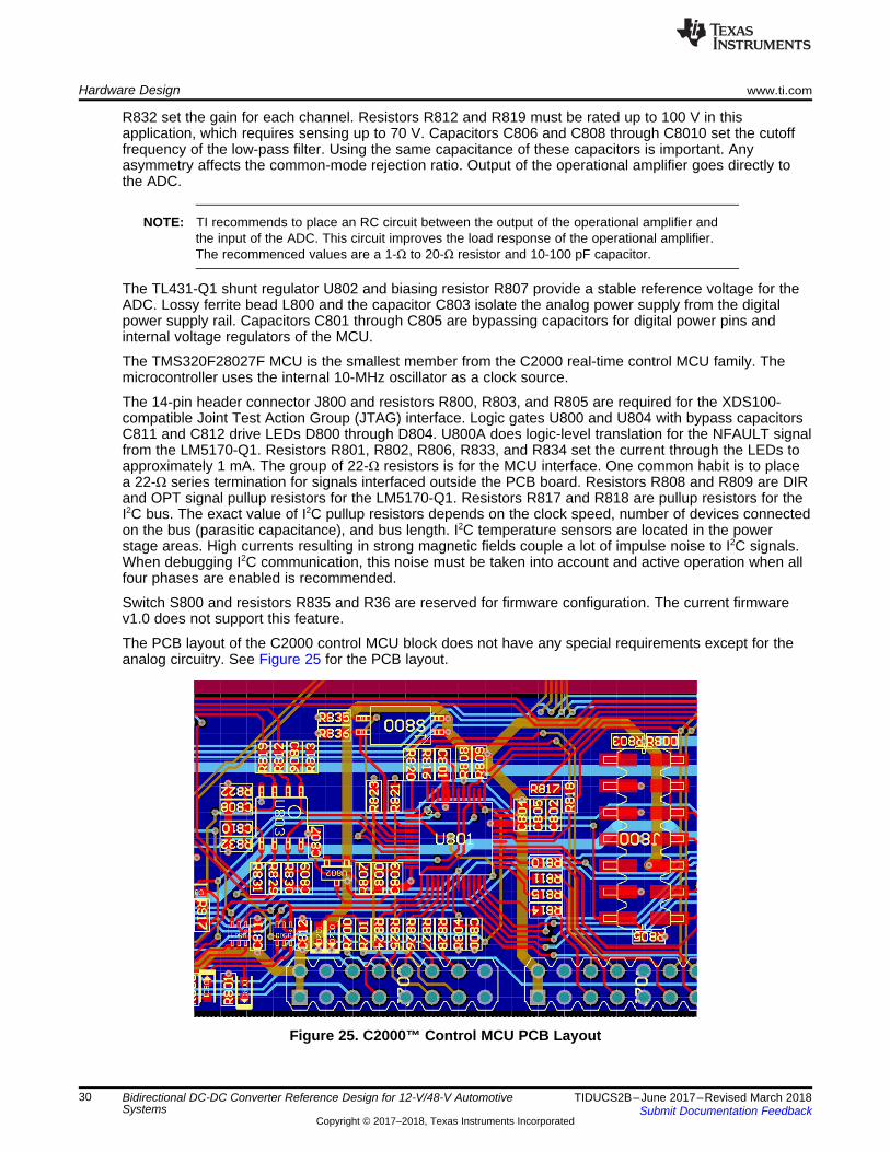
Hardware Design www.ti.com
30 TIDUCS2B–June 2017–Revised March 2018Submit Documentation Feedback
Copyright © 2017–2018, Texas Instruments Incorporated
Bidirectional DC-DC Converter Reference Design for 12-V/48-V AutomotiveSystems
R832 set the gain for each channel. Resistors R812 and R819 must be rated up to 100 V in thisapplication, which requires sensing up to 70 V. Capacitors C806 and C808 through C8010 set the cutofffrequency of the low-pass filter. Using the same capacitance of these capacitors is important. Anyasymmetry affects the common-mode rejection ratio. Output of the operational amplifier goes directly tothe ADC.
NOTE: TI recommends to place an RC circuit between the output of the operational amplifier andthe input of the ADC. This circuit improves the load response of the operational amplifier.The recommenced values are a 1-Ω to 20-Ω resistor and 10-100 pF capacitor.
The TL431-Q1 shunt regulator U802 and biasing resistor R807 provide a stable reference voltage for theADC. Lossy ferrite bead L800 and the capacitor C803 isolate the analog power supply from the digitalpower supply rail. Capacitors C801 through C805 are bypassing capacitors for digital power pins andinternal voltage regulators of the MCU.
The TMS320F28027F MCU is the smallest member from the C2000 real-time control MCU family. Themicrocontroller uses the internal 10-MHz oscillator as a clock source.
The 14-pin header connector J800 and resistors R800, R803, and R805 are required for the XDS100-compatible Joint Test Action Group (JTAG) interface. Logic gates U800 and U804 with bypass capacitorsC811 and C812 drive LEDs D800 through D804. U800A does logic-level translation for the NFAULT signalfrom the LM5170-Q1. Resistors R801, R802, R806, R833, and R834 set the current through the LEDs toapproximately 1 mA. The group of 22-Ω resistors is for the MCU interface. One common habit is to placea 22-Ω series termination for signals interfaced outside the PCB board. Resistors R808 and R809 are DIRand OPT signal pullup resistors for the LM5170-Q1. Resistors R817 and R818 are pullup resistors for theI2C bus. The exact value of I2C pullup resistors depends on the clock speed, number of devices connectedon the bus (parasitic capacitance), and bus length. I2C temperature sensors are located in the powerstage areas. High currents resulting in strong magnetic fields couple a lot of impulse noise to I2C signals.When debugging I2C communication, this noise must be taken into account and active operation when allfour phases are enabled is recommended.
Switch S800 and resistors R835 and R36 are reserved for firmware configuration. The current firmwarev1.0 does not support this feature.
The PCB layout of the C2000 control MCU block does not have any special requirements except for theanalog circuitry. See Figure 25 for the PCB layout.
Figure 25. C2000™ Control MCU PCB Layout
www.ti.com Hardware Design
31TIDUCS2B–June 2017–Revised March 2018Submit Documentation Feedback
Copyright © 2017–2018, Texas Instruments Incorporated
Bidirectional DC-DC Converter Reference Design for 12-V/48-V AutomotiveSystems
3.6.4 Test DataSee Section 6.4 for the test data.
3.6.5 Further ReadingSee the following resources for more information:1. Texas Instruments, C2000™ Real-Time Microcontrollers, C2000 MCU Brochure (SPRB176AD)
3.7 Diagnostics
3.7.1 DescriptionThe diagnostic block in TIDA-01168 monitors phase temperatures, MCU activity, reverse polarity conditionon the 12-V rail, and bias voltages for the MCU and LM5170-Q1 subsystems. See Table 10 for a systeminterface overview of the diagnostic block.
Table 10. System Interface for Diagnostic Block
SIGNAL DIRECTION DESCRIPTIONP3V3 In +3.3-V bias supplyGND — Common groundSDA In/Out I2C bus dataSCL In I2C bus clock
KL30_POL In Polarity detection for the 12-V batterynRST Out MCU reset
nSHDN Out Emergency shutdown for LM5170-Q1sWDT_TRIG In External watchdog timer trigger
3.7.2 ConsiderationsA basic set of diagnostic features and bias supply failure detection are beneficial even in a designintended for laboratory use. Temperature sensors monitor each power phase and react toovertemperature events independently of the control MCU. External reset circuitry with a watchdog timer isoften used in systems controlled by an MCU. In the event that the MCU does not react (locks up), forexample, due to a software bug or a control flow error, the watchdog timer shuts down the completesystem and keeps it in a safe state. An integrated watchdog timer in the MCU can also be used if theprovided level of robustness is sufficient. External watchdog circuit ICs are usually combined with voltagesupervisor functionality, which make them a very robust solution. Systems with ASIL requirements oftenuse a system basis chip (SBC). The SBC integrates even more functionality in a single chip, for examplelow-dropout regulators (LDOs), voltage supervisors, CAN and LIN interfaces, or wake-up signals.
Monitoring bias voltages for the MCU and LM5170-Q1 subsystems is important to ensure that allintegrated circuits operate only within the specified operating voltage range. Operating within the specifiedoperating range is important, especially during system start-up when all devices should be kept in reset orstandby mode until the bias voltages reach the preset value.
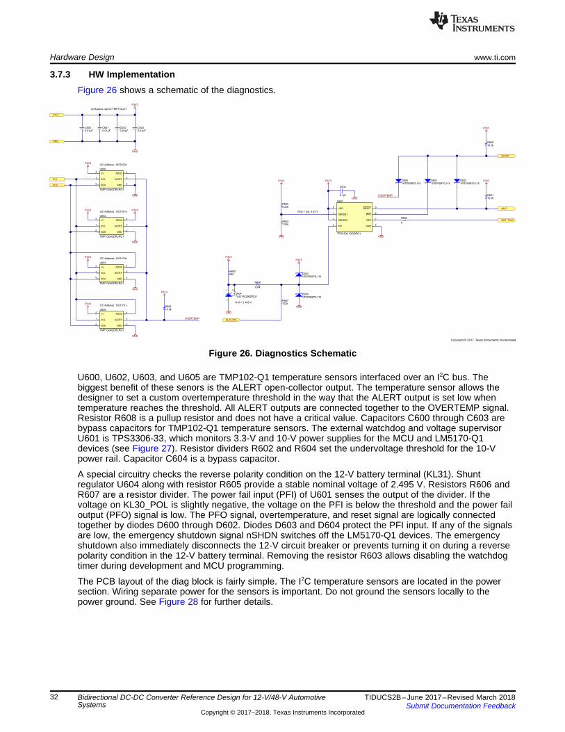
SCL1
GND2
ALERT3
ADD04
V+5
SDA6
U600
TMP102AQDRLRQ1
P3V3
0.01µFC600
SCL
SDA
GND
SCL1
GND2
ALERT3
ADD04
V+5
SDA6
U602
TMP102AQDRLRQ1
P3V3
SCL1
GND2
ALERT3
ADD04
V+5
SDA6
U603
TMP102AQDRLRQ1
P3V3
SCL1
GND2
ALERT3
ADD04
V+5
SDA6
U605
TMP102AQDRLRQ1
P3V3
0.01µFC601
0.01µFC602
0.01µFC603
P3V3
P3V3
4x Bypass cap for TMP102-Q1
I2C Address: 1001000x
I2C Address: 1001001x
I2C Address: 1001010x
I2C Address: 1001011x
P3V3
SENSE11
SENSE22
PFI3
GND4
RESET5
PFO6
WDI7
VDD8
U601
TPS3306-33QDRQ1
D6001PS79SB70,115
D6011PS79SB70,115
D6021PS79SB70,115
nSHDN
nRST
OVERTEMP
WDT_TRIG
P3V3
0.1µF
C604
GND
GND
OVERTEMP
10.0kR608
P3V3
13
2
U604TL431AQDBZRQ1
P3V3
GND
680R605
Vref = 2.495 V
P10V
8.20kR602
7.50kR604
GND
Vtrip = typ. 9.53 V
100k
R606
102kR607
D6041PS79SB70,115
GND
D6031PS79SB70,115
P3V3
KL30_POL
GND
GND
GND
GND
GND
10.0kR600
P3V3
10.0kR601
P3V3
0
R603
Copyright © 2017, Texas Instruments Incorporated
Hardware Design www.ti.com
32 TIDUCS2B–June 2017–Revised March 2018Submit Documentation Feedback
Copyright © 2017–2018, Texas Instruments Incorporated
Bidirectional DC-DC Converter Reference Design for 12-V/48-V AutomotiveSystems
3.7.3 HW ImplementationFigure 26 shows a schematic of the diagnostics.
Figure 26. Diagnostics Schematic
U600, U602, U603, and U605 are TMP102-Q1 temperature sensors interfaced over an I2C bus. Thebiggest benefit of these senors is the ALERT open-collector output. The temperature sensor allows thedesigner to set a custom overtemperature threshold in the way that the ALERT output is set low whentemperature reaches the threshold. All ALERT outputs are connected together to the OVERTEMP signal.Resistor R608 is a pullup resistor and does not have a critical value. Capacitors C600 through C603 arebypass capacitors for TMP102-Q1 temperature sensors. The external watchdog and voltage supervisorU601 is TPS3306-33, which monitors 3.3-V and 10-V power supplies for the MCU and LM5170-Q1devices (see Figure 27). Resistor dividers R602 and R604 set the undervoltage threshold for the 10-Vpower rail. Capacitor C604 is a bypass capacitor.
A special circuitry checks the reverse polarity condition on the 12-V battery terminal (KL31). Shuntregulator U604 along with resistor R605 provide a stable nominal voltage of 2.495 V. Resistors R606 andR607 are a resistor divider. The power fail input (PFI) of U601 senses the output of the divider. If thevoltage on KL30_POL is slightly negative, the voltage on the PFI is below the threshold and the power failoutput (PFO) signal is low. The PFO signal, overtemperature, and reset signal are logically connectedtogether by diodes D600 through D602. Diodes D603 and D604 protect the PFI input. If any of the signalsare low, the emergency shutdown signal nSHDN switches off the LM5170-Q1 devices. The emergencyshutdown also immediately disconnects the 12-V circuit breaker or prevents turning it on during a reversepolarity condition in the 12-V battery terminal. Removing the resistor R603 allows disabling the watchdogtimer during development and MCU programming.
The PCB layout of the diag block is fairly simple. The I2C temperature sensors are located in the powersection. Wiring separate power for the sensors is important. Do not ground the sensors locally to thepower ground. See Figure 28 for further details.
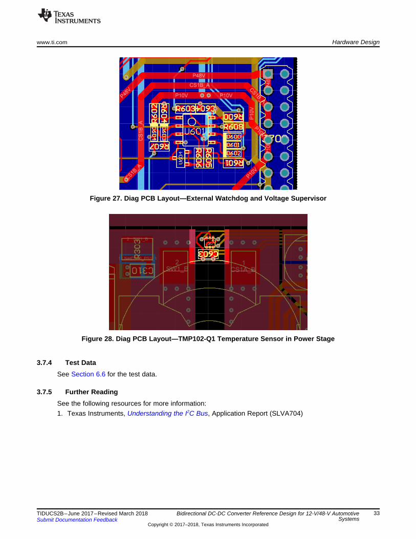
www.ti.com Hardware Design
33TIDUCS2B–June 2017–Revised March 2018Submit Documentation Feedback
Copyright © 2017–2018, Texas Instruments Incorporated
Bidirectional DC-DC Converter Reference Design for 12-V/48-V AutomotiveSystems
Figure 27. Diag PCB Layout—External Watchdog and Voltage Supervisor
Figure 28. Diag PCB Layout—TMP102-Q1 Temperature Sensor in Power Stage
3.7.4 Test DataSee Section 6.6 for the test data.
3.7.5 Further ReadingSee the following resources for more information:1. Texas Instruments, Understanding the I2C Bus, Application Report (SLVA704)
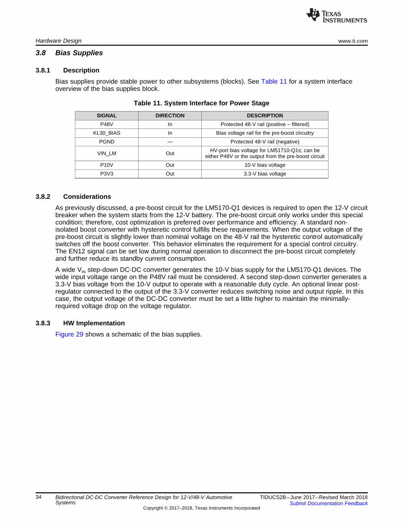
Hardware Design www.ti.com
34 TIDUCS2B–June 2017–Revised March 2018Submit Documentation Feedback
Copyright © 2017–2018, Texas Instruments Incorporated
Bidirectional DC-DC Converter Reference Design for 12-V/48-V AutomotiveSystems
3.8 Bias Supplies
3.8.1 DescriptionBias supplies provide stable power to other subsystems (blocks). See Table 11 for a system interfaceoverview of the bias supplies block.
Table 11. System Interface for Power Stage
SIGNAL DIRECTION DESCRIPTIONP48V In Protected 48-V rail (positive – filtered)
KL30_BIAS In Bias voltage rail for the pre-boost circuitryPGND — Protected 48-V rail (negative)
VIN_LM Out HV-port bias voltage for LM51710-Q1s; can beeither P48V or the output from the pre-boost circuit
P10V Out 10-V bias voltageP3V3 Out 3.3-V bias voltage
3.8.2 ConsiderationsAs previously discussed, a pre-boost circuit for the LM5170-Q1 devices is required to open the 12-V circuitbreaker when the system starts from the 12-V battery. The pre-boost circuit only works under this specialcondition; therefore, cost optimization is preferred over performance and efficiency. A standard non-isolated boost converter with hysteretic control fulfills these requirements. When the output voltage of thepre-boost circuit is slightly lower than nominal voltage on the 48-V rail the hysteretic control automaticallyswitches off the boost converter. This behavior eliminates the requirement for a special control circuitry.The EN12 signal can be set low during normal operation to disconnect the pre-boost circuit completelyand further reduce its standby current consumption.
A wide VIN step-down DC-DC converter generates the 10-V bias supply for the LM5170-Q1 devices. Thewide input voltage range on the P48V rail must be considered. A second step-down converter generates a3.3-V bias voltage from the 10-V output to operate with a reasonable duty cycle. An optional linear post-regulator connected to the output of the 3.3-V converter reduces switching noise and output ripple. In thiscase, the output voltage of the DC-DC converter must be set a little higher to maintain the minimally-required voltage drop on the voltage regulator.
3.8.3 HW ImplementationFigure 29 shows a schematic of the bias supplies.
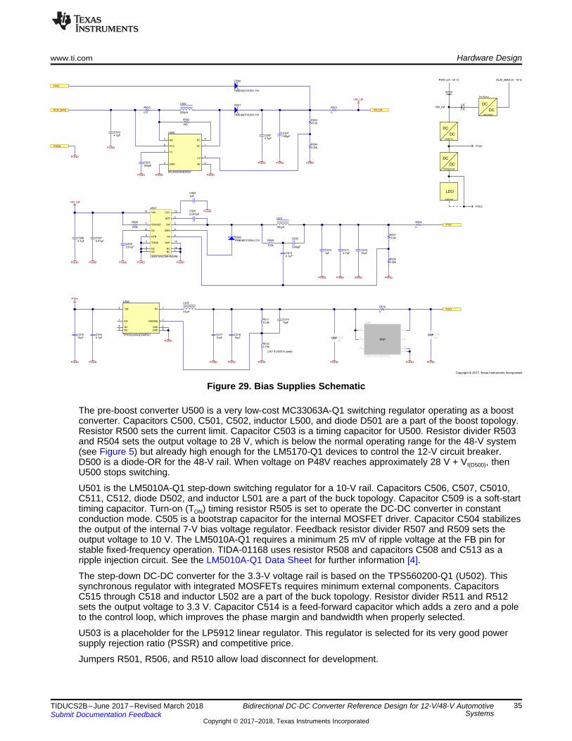
SC1
SE2
TC3
GND4
CII5
VCC6
Ipk7
DC8
U500
MC33063AQDRQ1
D500
PMEG6010CEH,115
D501
PMEG6010CEH,115
KL30_BIAS
PGND
220µH
L500
47.0kR503
0.5
R500
390pFC503
PGND
180
R502
PGND
2.20kR504
PGND
180µFC501
PGND
P48V
VIN_LM
PGND
PGND
VCC12
SS10
SW2
FB9
RTN6
VIN13
BST3
RON/SD11
DAP15
NC1
NC7
NC8
NC14
ISEN4
SGND5
U501
LM5010AQ1MH/NOPB
10.0kR507
3.32kR509
180µH
L501
0.01µFC509
PGND
0.01µFC507
4.7µFC506
PGND PGND
PGND
D502PMEG6010CEH,115
PGND
0.1µFC513
100k
R508
PGND PGND
PGNDPGND
P10V
1µFC504
PGND0.047µFC505
VIN_LM
VIN_LM
169k
R505
4.7µFC511
1µFC510
10µFC512
EN1
GND2
PH7
VIN6
VSENSE3
NC4
NC5
GND8
U502
TPS560200QDGKRQ1
PGND
10.0kR511
3.16kR512
PGNDPGND
P3V3
10µFC518
10µFC517
PGND
33µH
L502
DC
DCMC33063
0.1µFC516
10µFC515
PGNDPGND
P10V
KL30_BIAS (6 - 18 V)P48V (24 - 54 V)
DC
DCLM5010
DC
DCTPS560200
P10V
VIN_LM
LDO
Optional
P3V3
Pre-Boost
3300pF
C508
0
R501
0
R506
0
R510
4.7µFC502
PGND
15pFC514
OUT1
NC2
PG3
EN4
GND5
IN6
PAD7
U503
LP5912Q3.3DRVRQ1
DNP
PGND
1µFC520DNP 1µF
C519DNP
PGNDPGND
4.7µFC500
PGND
(2k7 if U503 is used)
Copyright © 2017, Texas Instruments Incorporated
www.ti.com Hardware Design
35TIDUCS2B–June 2017–Revised March 2018Submit Documentation Feedback
Copyright © 2017–2018, Texas Instruments Incorporated
Bidirectional DC-DC Converter Reference Design for 12-V/48-V AutomotiveSystems
Figure 29. Bias Supplies Schematic
The pre-boost converter U500 is a very low-cost MC33063A-Q1 switching regulator operating as a boostconverter. Capacitors C500, C501, C502, inductor L500, and diode D501 are a part of the boost topology.Resistor R500 sets the current limit. Capacitor C503 is a timing capacitor for U500. Resistor divider R503and R504 sets the output voltage to 28 V, which is below the normal operating range for the 48-V system(see Figure 5) but already high enough for the LM5170-Q1 devices to control the 12-V circuit breaker.D500 is a diode-OR for the 48-V rail. When voltage on P48V reaches approximately 28 V + Vf(D500), thenU500 stops switching.
U501 is the LM5010A-Q1 step-down switching regulator for a 10-V rail. Capacitors C506, C507, C5010,C511, C512, diode D502, and inductor L501 are a part of the buck topology. Capacitor C509 is a soft-starttiming capacitor. Turn-on (TON) timing resistor R505 is set to operate the DC-DC converter in constantconduction mode. C505 is a bootstrap capacitor for the internal MOSFET driver. Capacitor C504 stabilizesthe output of the internal 7-V bias voltage regulator. Feedback resistor divider R507 and R509 sets theoutput voltage to 10 V. The LM5010A-Q1 requires a minimum 25 mV of ripple voltage at the FB pin forstable fixed-frequency operation. TIDA-01168 uses resistor R508 and capacitors C508 and C513 as aripple injection circuit. See the LM5010A-Q1 Data Sheet for further information [4].
The step-down DC-DC converter for the 3.3-V voltage rail is based on the TPS560200-Q1 (U502). Thissynchronous regulator with integrated MOSFETs requires minimum external components. CapacitorsC515 through C518 and inductor L502 are a part of the buck topology. Resistor divider R511 and R512sets the output voltage to 3.3 V. Capacitor C514 is a feed-forward capacitor which adds a zero and a poleto the control loop, which improves the phase margin and bandwidth when properly selected.
U503 is a placeholder for the LP5912 linear regulator. This regulator is selected for its very good powersupply rejection ratio (PSSR) and competitive price.
Jumpers R501, R506, and R510 allow load disconnect for development.
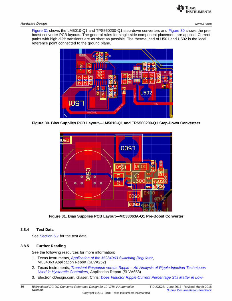
Hardware Design www.ti.com
36 TIDUCS2B–June 2017–Revised March 2018Submit Documentation Feedback
Copyright © 2017–2018, Texas Instruments Incorporated
Bidirectional DC-DC Converter Reference Design for 12-V/48-V AutomotiveSystems
Figure 31 shows the LM5010-Q1 and TPS560200-Q1 step-down converters and Figure 30 shows the pre-boost converter PCB layouts. The general rules for single-side component placement are applied. Currentpaths with high di/dt transients are as short as possible. The thermal pad of U501 and U502 is the localreference point connected to the ground plane.
Figure 30. Bias Supplies PCB Layout—LM5010-Q1 and TPS560200-Q1 Step-Down Converters
Figure 31. Bias Supplies PCB Layout—MC33063A-Q1 Pre-Boost Converter
3.8.4 Test DataSee Section 6.7 for the test data.
3.8.5 Further ReadingSee the following resources for more information:1. Texas Instruments, Application of the MC34063 Switching Regulator,
MC34063 Application Report (SLVA252)2. Texas Instruments, Transient Response versus Ripple – An Analysis of Ripple Injection Techniques
Used in Hysteretic Controllers, Application Report (SLVA653)3. ElectronicDesign.com, Glaser, Chris; Does Inductor Ripple-Current Percentage Still Matter in Low-
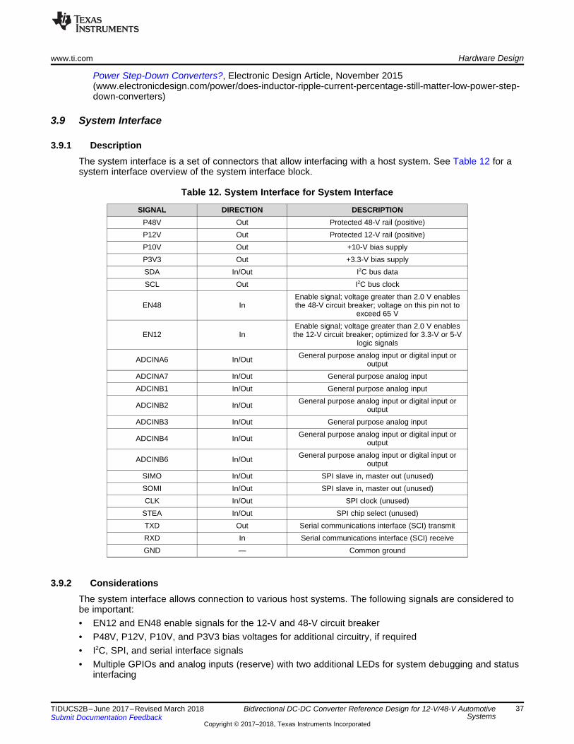
www.ti.com Hardware Design
37TIDUCS2B–June 2017–Revised March 2018Submit Documentation Feedback
Copyright © 2017–2018, Texas Instruments Incorporated
Bidirectional DC-DC Converter Reference Design for 12-V/48-V AutomotiveSystems
Power Step-Down Converters?, Electronic Design Article, November 2015(www.electronicdesign.com/power/does-inductor-ripple-current-percentage-still-matter-low-power-step-down-converters)
3.9 System Interface
3.9.1 DescriptionThe system interface is a set of connectors that allow interfacing with a host system. See Table 12 for asystem interface overview of the system interface block.
Table 12. System Interface for System Interface
SIGNAL DIRECTION DESCRIPTIONP48V Out Protected 48-V rail (positive)P12V Out Protected 12-V rail (positive)P10V Out +10-V bias supplyP3V3 Out +3.3-V bias supplySDA In/Out I2C bus dataSCL Out I2C bus clock
EN48 InEnable signal; voltage greater than 2.0 V enablesthe 48-V circuit breaker; voltage on this pin not to
exceed 65 V
EN12 InEnable signal; voltage greater than 2.0 V enablesthe 12-V circuit breaker; optimized for 3.3-V or 5-V
logic signals
ADCINA6 In/Out General purpose analog input or digital input oroutput
ADCINA7 In/Out General purpose analog inputADCINB1 In/Out General purpose analog input
ADCINB2 In/Out General purpose analog input or digital input oroutput
ADCINB3 In/Out General purpose analog input
ADCINB4 In/Out General purpose analog input or digital input oroutput
ADCINB6 In/Out General purpose analog input or digital input oroutput
SIMO In/Out SPI slave in, master out (unused)SOMI In/Out SPI slave in, master out (unused)CLK In/Out SPI clock (unused)
STEA In/Out SPI chip select (unused)TXD Out Serial communications interface (SCI) transmitRXD In Serial communications interface (SCI) receiveGND — Common ground
3.9.2 ConsiderationsThe system interface allows connection to various host systems. The following signals are considered tobe important:• EN12 and EN48 enable signals for the 12-V and 48-V circuit breaker• P48V, P12V, P10V, and P3V3 bias voltages for additional circuitry, if required• I2C, SPI, and serial interface signals• Multiple GPIOs and analog inputs (reserve) with two additional LEDs for system debugging and status
interfacing
P3V3
EN12
P12V
P48V
GND
ADCINB3ADCINB2
ADCINB6ADCINB4
GND GND
1 2
3 4
5 6
7 8
9 10
11 12
13 14
15 16
J700PRPC008DAAN-RC
GND
P10V
1 2
3 4
5 6
7 8
9 10
11 12
13 14
15 16
J701PRPC008DAAN-RC
GND
GND
GNDGND
GND
GND
P3V3 P3V3
1 2
3 4
5 6
7 8
9 10
11 12
13 14
15 16
J702PRPC008DAAN-RC
GND
GND
GND
P3V3P3V3GND
Green
21
D700
680R700
Green
21
D701
680R701
RXDTXD
SDASCL
EN48ADCINB1
CLK
SIMOSOMI
STEA
ADCINA7ADCINA6
Copyright © 2017, Texas Instruments Incorporated
Hardware Design www.ti.com
38 TIDUCS2B–June 2017–Revised March 2018Submit Documentation Feedback
Copyright © 2017–2018, Texas Instruments Incorporated
Bidirectional DC-DC Converter Reference Design for 12-V/48-V AutomotiveSystems
3.9.3 HW ImplementationFigure 29 shows a schematic of the system interface.
Figure 32. System Interface Schematic
Connectors J700 through J702 are standard through hole 2x8 pin headers with 100-mil spacing. LEDdiodes D700 and D701 are for debugging purposes and the user interface. Resistors R700 and R701 setthe current through the LEDs to approximately 1 mA. All connectors have multiple ground signals for theoptimal current return path.
3.9.4 Test DataTest data for the 48-V block is not available and is a subject for future update.
Module: tmp102.c Module: serial.c
Module: main.c
Module: control.c
ePWM GPIO ADC I2C UART ...
Module: hal.c
Interface: tmp102.h Interface: serial.h
Interface: hal.h
System Control: Comp, CtrlPrm
Interface: control.h
execute
read & update
execute
update
execute
update
executeupdate execute
update
execute
update
Direct R/W Hardware Access
App
licat
ion
Driv
er /
Con
trol
HW
Abs
trac
tion
MC
U
Laye
rLa
yer
Laye
rLa
yer
www.ti.com Software Design
39TIDUCS2B–June 2017–Revised March 2018Submit Documentation Feedback
Copyright © 2017–2018, Texas Instruments Incorporated
Bidirectional DC-DC Converter Reference Design for 12-V/48-V AutomotiveSystems
4 Software DesignThe software for the TIDA-01168 design enables basic functionality and a simple interface to a hostsystem. The following subsections focus on the overall system architecture and voltage control loop. Thesoftware is written in C programming language and compiled using 16.9.1. LTS C2000 compiler in CodeComposer Studio™ software 7.0.0.00043 from Texas Instruments.
NOTE: The software for TIDA-01168 is developed for demonstration purposes only. TexasInstruments provides no warranty for using this software.
4.1 ArchitectureThe software architecture for the TIDA-01168 design follows a minimalist approach, using a layerarchitecture as shown in Figure 33. The system does not use any real-time operating system or anextensive set of additional software libraries. Understanding the concept allows for easy modification andcode porting to a different MCU.
Figure 33. Software Architecture Diagram for TIDA-01168
The software architecture is split into four layers (see Figure 33):• Application Layer – (Module main)• Driver/Control Layer – (Modules tmp102, control, serial)• Hardware Abstraction Layer – (Module hal)• MCU Layer – (TMS320F28027 registers and peripherals)Communication between layers is from the top to the bottom with the given module interface. TheApplication Layer and Driver/Control Layer are hardware independent. Any access to the MCU registers orperipherals is in the HW Abstraction layer. This layer uses a set of functions and macros for direct accessto the MCU Layer (MCU architecture). Only the HW Abstraction layer requires modification for migratingthe software to a different MCU (changing the MCU layer).
The software uses a fixed-point Q number format for decimal numbers. All arithmetic operations withdecimal numbers use C28X IQmath Library from Texas Instruments. This library is free of charge. See theC28x IQmath Library user's guide for further details [5].
Software Design www.ti.com
40 TIDUCS2B–June 2017–Revised March 2018Submit Documentation Feedback
Copyright © 2017–2018, Texas Instruments Incorporated
Bidirectional DC-DC Converter Reference Design for 12-V/48-V AutomotiveSystems
4.2 The Super Loop (Main Loop)The MCU executes the code in an endless main loop (super-loop architecture) with only two interrupts.The first interrupt is used for the control loop while the second is used for serial communication. Two mainvariables-structures Comp and CtrlPrm exist, which define system behavior and configuration. The type ofthese variables is declared in the control module header file and defined in the main module. SeeTable 13 and Table 14 for the description.
NOTE: Q numbers have finite resolution given by the number of bits after the decimal point. Thisfact results in the arithmetic rounding of preset and calculated values.
Table 13. Configuration Variable CtrlPrm
NAME TYPE TYPICAL VALUES DESCRIPTIONVoltage, Current, and Temperature Measurements
CtrlPrm.Meas.P12Vraw Uint16 0…4095 P12V voltage AD conversion result after median-filteringCtrlPrm.Meas.P48Vraw Uint16 0…4095 P48V voltage AD conversion result after median-filtering
CtrlPrm.Meas.IMONraw Uint16 0…4095 IMON voltage (current) AD conversion result aftermedian-filtering
CtrlPrm.Meas.P12Vscaled Q24 0…2.495 P12V voltage ADC result normalized to the voltagereference
CtrlPrm.Meas.P48Vscaled Q24 0…2.495 P48V voltage ADC result normalized to the voltagereference
CtrlPrm.Meas.IMONscaled Q24 0…2.495 IMON voltage (current) ADC result normalized to thevoltage reference
CtrlPrm.Meas.P12Vvoltage Q24 0…24.95 P12V voltage in Q number formatCtrlPrm.Meas.P48Vvoltage Q24 0…75.10 P48V voltage in Q number formatCtrlPrm.Meas.IMONcurrent Q23 0…175.685 IMON current in Q number format
CtrlPrm.Meas.TempPS1 Q4 –40…+125 Power stage 1 temperature in Q number formatCtrlPrm.Meas.TempPS2 Q4 –40…+125 Power stage 2 temperature in Q number formatCtrlPrm.Meas.TempPS3 Q4 –40…+125 Power stage 3 temperature in Q number formatCtrlPrm.Meas.TempPS4 Q4 –40…+125 Power stage 4 temperature in Q number format
Control ParametersCtrlPrm.Ctrl.P12Vset Q24 6…18 Pre-set P12V output voltage for the BUCK modeCtrlPrm.Ctrl.P48Vset Q24 24…54 Pre-set P48V output voltage for the BOOST mode
CtrlPrm.Ctrl.NoOfPhases Uint16 (3bits) 0…4 Number of active phases
CtrlPrm.Ctrl.UVLOtrack Uint16 (1bit) 0/1 Real-time logic level of UVLO signal
CtrlPrm.Ctrl.nFAULTtrack Uint16 (1bit) 0/1 Real-time logic level of nFAULT signal
CtrlPrm.Ctrl.Mode Uint16 (1bit) 0/1 (1 = Buck, 0 = Boost) Buck or boost operation mode
CtrlPrm.Ctrl.RefershTrig Uint16 (1bit)
Write 1, automaticallyclears to 0 when updated
Confirmation for the semi-synchronous control loop thatLM5170-Q1 GPIOs shall be updated
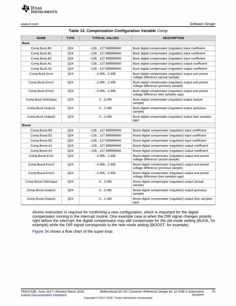
www.ti.com Software Design
41TIDUCS2B–June 2017–Revised March 2018Submit Documentation Feedback
Copyright © 2017–2018, Texas Instruments Incorporated
Bidirectional DC-DC Converter Reference Design for 12-V/48-V AutomotiveSystems
Table 14. Compensation Configuration Variable Comp
NAME TYPE TYPICAL VALUES DESCRIPTIONBuck
Comp.Buck.B0 Q24 –128…127.999999940 Buck digital compensator (regulator) input coefficientComp.Buck.B1 Q24 –128…127.999999940 Buck digital compensator (regulator) input coefficientComp.Buck.B2 Q24 –128…127.999999940 Buck digital compensator (regulator) input coefficientComp.Buck.A1 Q24 –128…127.999999940 Buck digital compensator (regulator) output coefficientComp.Buck.A2 Q24 –128…127.999999940 Buck digital compensator (regulator) output coefficient
Comp.Buck.Error Q24 –2.495…2.495 Buck digital compensator (regulator) output and presetvoltage difference (actual sample)
Comp.Buck.Error1 Q24 –2.495…2.495 Buck digital compensator (regulator) output and presetvoltage difference (previous sample)
Comp.Buck.Error2 Q24 –2.495…2.495 Buck digital compensator (regulator) output and presetvoltage difference (two samples ago)
Comp.Buck.SetOutput Q24 0…2.495 Buck digital compensator (regulator) output (actualsample)
Comp.Buck.Output1 Q24 0…2.495 Buck digital compensator (regulator) output (previoussample)
Comp.Buck.Output2 Q24 0…2.495 Buck digital compensator (regulator) output (two samplesago)
BoostComp.Boost.B0 Q24 –128…127.999999940 Boost digital compensator (regulator) input coefficientComp.Boost.B1 Q24 –128…127.999999940 Boost digital compensator (regulator) input coefficientComp.Boost.B2 Q24 –128…127.999999940 Boost digital compensator (regulator) input coefficientComp.Boost.A1 Q24 –128…127.999999940 Boost digital compensator (regulator) output coefficientComp.Boost.A2 Q24 –128…127.999999940 Boost digital compensator (regulator) output coefficient
Comp.Boost.Error Q24 –2.495…2.495 Boost digital compensator (regulator) output and presetvoltage difference (actual sample)
Comp.Boost.Error1 Q24 –2.495…2.495 Boost digital compensator (regulator) output and presetvoltage difference (previous sample)
Comp.Boost.Error2 Q24 –2.495…2.495 Boost digital compensator (regulator) output and presetvoltage difference (two samples ago)
Comp.Boost.SetOutput Q24 0…2.495 Boost digital compensator (regulator) output (actualsample)
Comp.Boost.Output1 Q24 0…2.495 Boost digital compensator (regulator) output (previoussample)
Comp.Boost.Output1 Q24 0…2.495 Boost digital compensator (regulator) output (two samplesago)
Atomic instruction is required for confirming a new configuration, which is important for the digitalcompensator running in the interrupt routine. One example case is when the DIR signal changes polarityright before the interrupt; the digital compensator may still compensate for the old mode setting (BUCK, forexample) while the DIR signal corresponds to the new mode setting (BOOST, for example).
Figure 34 shows a flow chart of the super-loop.
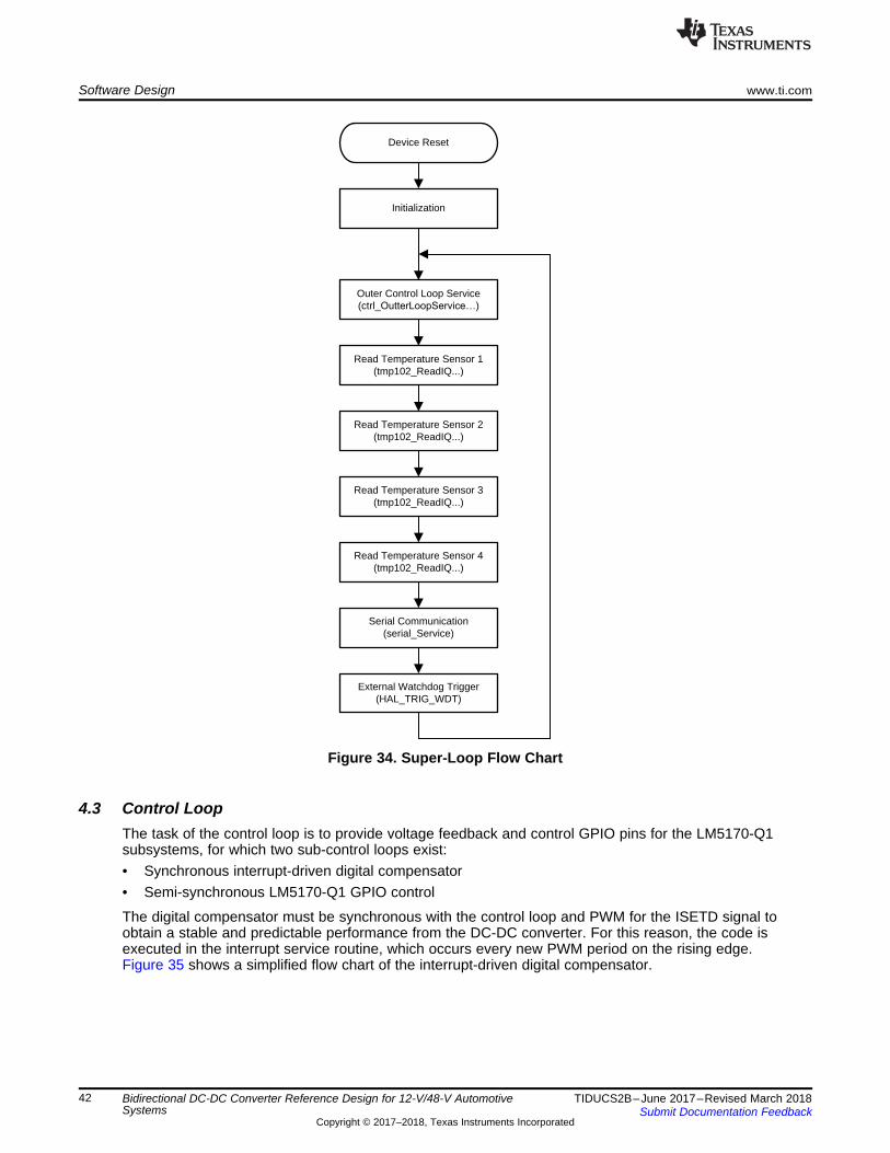
Outer Control Loop Service(ctrl_2XWWHU/RRS6HUYLFH«)
Read Temperature Sensor 1(tmp102_ReadIQ...)
Read Temperature Sensor 2(tmp102_ReadIQ...)
Read Temperature Sensor 3(tmp102_ReadIQ...)
Read Temperature Sensor 4(tmp102_ReadIQ...)
Serial Communication(serial_Service)
External Watchdog Trigger(HAL_TRIG_WDT)
Initialization
Device Reset
Software Design www.ti.com
42 TIDUCS2B–June 2017–Revised March 2018Submit Documentation Feedback
Copyright © 2017–2018, Texas Instruments Incorporated
Bidirectional DC-DC Converter Reference Design for 12-V/48-V AutomotiveSystems
Figure 34. Super-Loop Flow Chart
4.3 Control LoopThe task of the control loop is to provide voltage feedback and control GPIO pins for the LM5170-Q1subsystems, for which two sub-control loops exist:• Synchronous interrupt-driven digital compensator• Semi-synchronous LM5170-Q1 GPIO control
The digital compensator must be synchronous with the control loop and PWM for the ISETD signal toobtain a stable and predictable performance from the DC-DC converter. For this reason, the code isexecuted in the interrupt service routine, which occurs every new PWM period on the rising edge.Figure 35 shows a simplified flow chart of the interrupt-driven digital compensator.
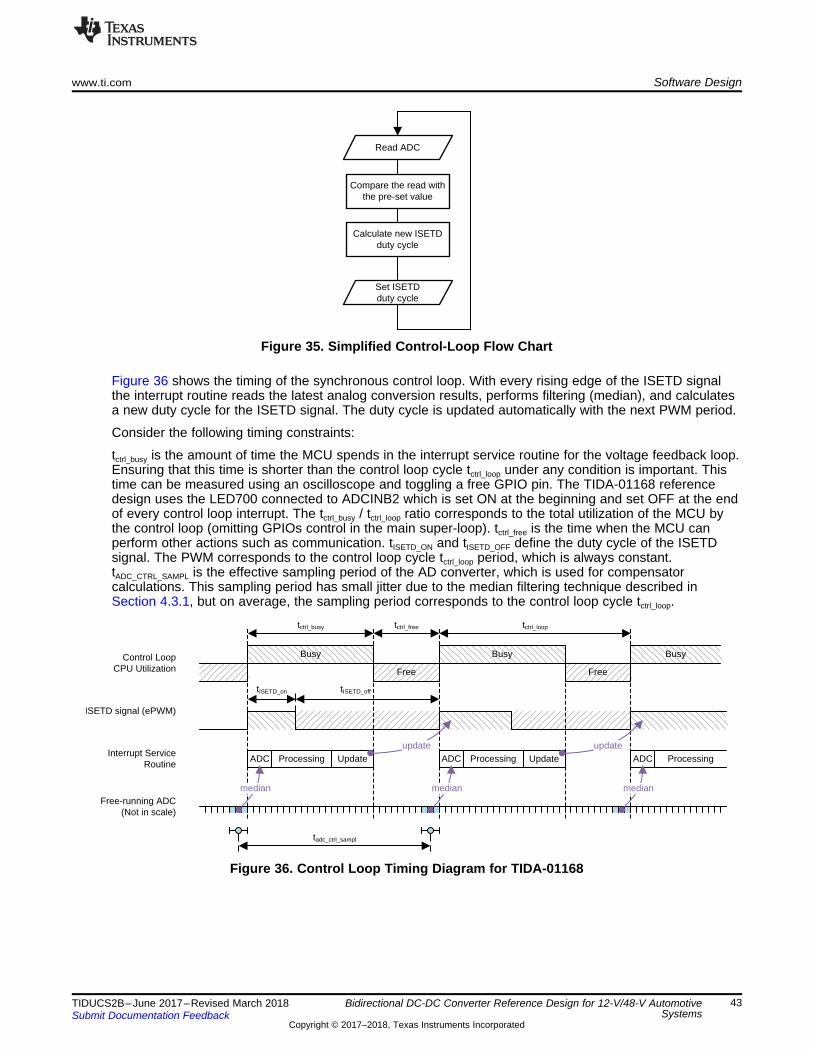
Busy
Free
Free-running ADC (Not in scale)
Interrupt Service Routine
ISETD signal (ePWM)
Processing Update
Control Loop CPU Utilization
update
Busy
Free
Busy
ADC
median
tISETD_on tISETD_off
Processing Updateupdate
ADC
median
ADC
median
tadc_ctrl_sampl
tctrl_busy tctrl_free tctrl_loop
Processing
Read ADC
Compare the read with the pre-set value
Calculate new ISETD duty cycle
Set ISETD duty cycle
www.ti.com Software Design
43TIDUCS2B–June 2017–Revised March 2018Submit Documentation Feedback
Copyright © 2017–2018, Texas Instruments Incorporated
Bidirectional DC-DC Converter Reference Design for 12-V/48-V AutomotiveSystems
Figure 35. Simplified Control-Loop Flow Chart
Figure 36 shows the timing of the synchronous control loop. With every rising edge of the ISETD signalthe interrupt routine reads the latest analog conversion results, performs filtering (median), and calculatesa new duty cycle for the ISETD signal. The duty cycle is updated automatically with the next PWM period.
Consider the following timing constraints:
tctrl_busy is the amount of time the MCU spends in the interrupt service routine for the voltage feedback loop.Ensuring that this time is shorter than the control loop cycle tctrl_loop under any condition is important. Thistime can be measured using an oscilloscope and toggling a free GPIO pin. The TIDA-01168 referencedesign uses the LED700 connected to ADCINB2 which is set ON at the beginning and set OFF at the endof every control loop interrupt. The tctrl_busy / tctrl_loop ratio corresponds to the total utilization of the MCU bythe control loop (omitting GPIOs control in the main super-loop). tctrl_free is the time when the MCU canperform other actions such as communication. tISETD_ON and tISETD_OFF define the duty cycle of the ISETDsignal. The PWM corresponds to the control loop cycle tctrl_loop period, which is always constant.tADC_CTRL_SAMPL is the effective sampling period of the AD converter, which is used for compensatorcalculations. This sampling period has small jitter due to the median filtering technique described inSection 4.3.1, but on average, the sampling period corresponds to the control loop cycle tctrl_loop.
Figure 36. Control Loop Timing Diagram for TIDA-01168
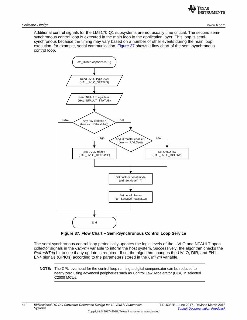
Set UVLO High-z(HAL_UVLO_RELEASE)
ctrl_OutterLoopService(«)
Read UVLO logic level(HAL_UVLO_STATUS)
Read NFAULT logic level(HAL_NFAULT_STATUS)
UVLO master enable ?(low == ..UVLOset)
Set UVLO low(HAL_UVLO_OCLOW)
Set buck or boost mode(ctrl_SetMode(«))
Set no. of phases (ctrl_SetNoOfPhases(«))
End
LowHigh
Any HW updates?(true == ..RefreshTrig)
TrueFalse
Software Design www.ti.com
44 TIDUCS2B–June 2017–Revised March 2018Submit Documentation Feedback
Copyright © 2017–2018, Texas Instruments Incorporated
Bidirectional DC-DC Converter Reference Design for 12-V/48-V AutomotiveSystems
Additional control signals for the LM5170-Q1 subsystems are not usually time critical. The second semi-synchronous control loop is executed in the main loop in the application layer. This loop is semi-synchronous because the timing may vary based on a number of other events during the main loopexecution, for example, serial communication. Figure 37 shows a flow chart of the semi-synchronouscontrol loop.
Figure 37. Flow Chart – Semi-Synchronous Control Loop Service
The semi-synchronous control loop periodically updates the logic levels of the UVLO and NFAULT opencollector signals in the CtrlPrm variable to inform the host system. Successively, the algorithm checks theRefreshTrig bit to see if any update is required. If so, the algorithm changes the UVLO, DIR, and EN1-EN4 signals (GPIOs) according to the parameters stored in the CtrlPrm variable.
NOTE: The CPU overhead for the control loop running a digital compensator can be reduced tonearly zero using advanced peripheries such as Control Law Accelerator (CLA) in selectedC2000 MCUs.
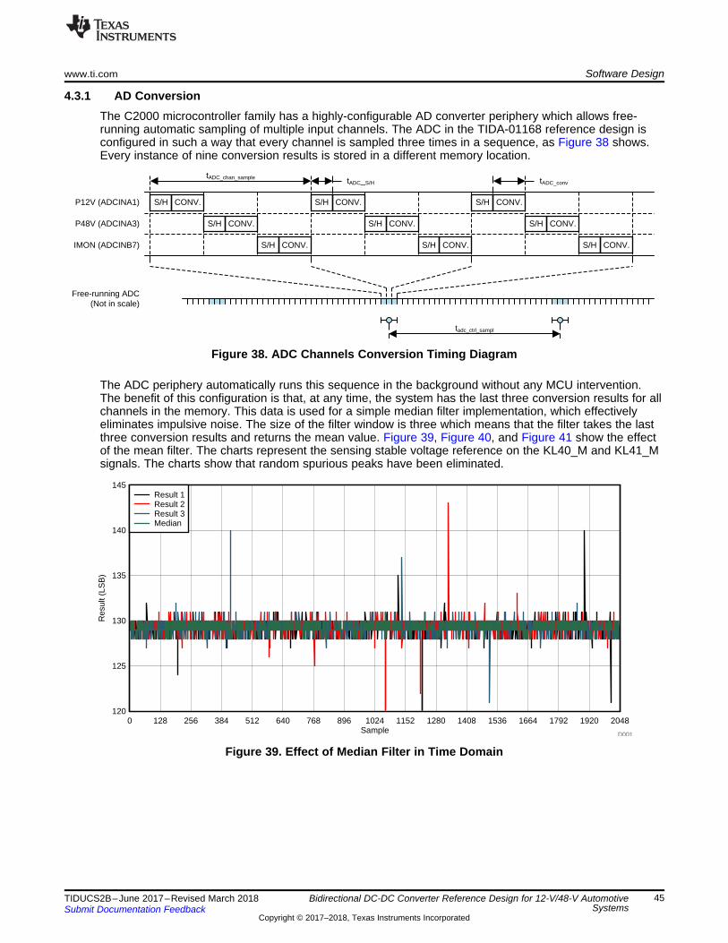
Sample
Res
ult (
LSB
)
0 128 256 384 512 640 768 896 1024 1152 1280 1408 1536 1664 1792 1920 2048120
125
130
135
140
145
D001D001
Result 1Result 2Result 3Median
CONV.
IMON (ADCINB7)
P48V (ADCINA3)
P12V (ADCINA1)
S/H CONV.
S/H CONV.
S/H CONV.
S/H CONV.
S/H CONV.
S/H CONV.
S/H CONV.
S/H CONV.
S/H
tADC_chan_sample
Free-running ADC (Not in scale)
tADC_S/H tADC_conv
tadc_ctrl_sampl
www.ti.com Software Design
45TIDUCS2B–June 2017–Revised March 2018Submit Documentation Feedback
Copyright © 2017–2018, Texas Instruments Incorporated
Bidirectional DC-DC Converter Reference Design for 12-V/48-V AutomotiveSystems
4.3.1 AD ConversionThe C2000 microcontroller family has a highly-configurable AD converter periphery which allows free-running automatic sampling of multiple input channels. The ADC in the TIDA-01168 reference design isconfigured in such a way that every channel is sampled three times in a sequence, as Figure 38 shows.Every instance of nine conversion results is stored in a different memory location.
Figure 38. ADC Channels Conversion Timing Diagram
The ADC periphery automatically runs this sequence in the background without any MCU intervention.The benefit of this configuration is that, at any time, the system has the last three conversion results for allchannels in the memory. This data is used for a simple median filter implementation, which effectivelyeliminates impulsive noise. The size of the filter window is three which means that the filter takes the lastthree conversion results and returns the mean value. Figure 39, Figure 40, and Figure 41 show the effectof the mean filter. The charts represent the sensing stable voltage reference on the KL40_M and KL41_Msignals. The charts show that random spurious peaks have been eliminated.
Figure 39. Effect of Median Filter in Time Domain
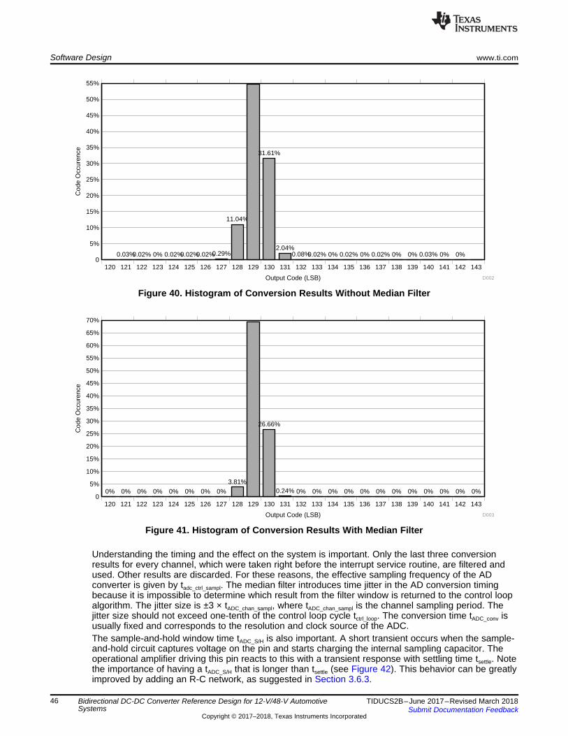
Output Code (LSB)
Cod
e O
ccur
ence
0
5%
10%
15%
20%
25%
30%
35%
40%
45%
50%
55%
60%
65%
70%
120 121 122 123 124 125 126 127 128 129 130 131 132 133 134 135 136 137 138 139 140 141 142 143
0% 0% 0% 0% 0% 0% 0% 0%
3.81%
26.66%
0.24% 0% 0% 0% 0% 0% 0% 0% 0% 0% 0% 0% 0%
D003
Output Code (LSB)
Cod
e O
ccur
ence
0
5%
10%
15%
20%
25%
30%
35%
40%
45%
50%
55%
120 121 122 123 124 125 126 127 128 129 130 131 132 133 134 135 136 137 138 139 140 141 142 143
0.03%0.02% 0% 0.02%0.02%0.02%0.29%
11.04%
31.61%
2.04%0.08%0.02% 0% 0.02% 0% 0.02% 0% 0% 0.03% 0% 0%
D002
Software Design www.ti.com
46 TIDUCS2B–June 2017–Revised March 2018Submit Documentation Feedback
Copyright © 2017–2018, Texas Instruments Incorporated
Bidirectional DC-DC Converter Reference Design for 12-V/48-V AutomotiveSystems
Figure 40. Histogram of Conversion Results Without Median Filter
Figure 41. Histogram of Conversion Results With Median Filter
Understanding the timing and the effect on the system is important. Only the last three conversionresults for every channel, which were taken right before the interrupt service routine, are filtered andused. Other results are discarded. For these reasons, the effective sampling frequency of the ADconverter is given by tadc_ctrl_sampl. The median filter introduces time jitter in the AD conversion timingbecause it is impossible to determine which result from the filter window is returned to the control loopalgorithm. The jitter size is ±3 × tADC_chan_sampl, where tADC_chan_sampl is the channel sampling period. Thejitter size should not exceed one-tenth of the control loop cycle tctrl_loop. The conversion time tADC_conv isusually fixed and corresponds to the resolution and clock source of the ADC.The sample-and-hold window time tADC_S/H is also important. A short transient occurs when the sample-and-hold circuit captures voltage on the pin and starts charging the internal sampling capacitor. Theoperational amplifier driving this pin reacts to this with a transient response with settling time tsettle. Notethe importance of having a tADC_S/H that is longer than tsettle (see Figure 42). This behavior can be greatlyimproved by adding an R-C network, as suggested in Section 3.6.3.
CONV.S/H CONV.S/H
tADC_S/H
tADC_chan_sample
tsettle tADC_conv
t
ADCINx
www.ti.com Software Design
47TIDUCS2B–June 2017–Revised March 2018Submit Documentation Feedback
Copyright © 2017–2018, Texas Instruments Incorporated
Bidirectional DC-DC Converter Reference Design for 12-V/48-V AutomotiveSystems
Figure 42. Sample-and-Hold Circuit Timing
4.3.2 Digital CompensatorA DC-DC converter is a closed-loop system that requires frequency compensation for the control loop toremain stable under any circumstances and to provide the desired step response.
Design procedure:1. Compensate the inner current loop
• Same compensation loop regardless of BUCK or BOOST mode2. Compensate the outer voltage loop
• Separate error amplifiers for each mode of operation• Low frequency pole is major concern in BUCK mode• Beware of right-half-plane zero (RHPZ) in BOOST model
The inner current control loop uses analog compensation as described in the LM5170-Q1 data sheet [2].The following selections are applied for the analog compensation and offer a good trade-off betweentransient response and stability:• Crossover frequency fc_curr for the inner current loop is 1/6th of the switching frequency fsw
• Compensation zero frequency fz1_curr is set to half of the crossover frequency fc_curr
• Compensation pole frequency fp1_curr is between half of the switching frequency fsw and switchingfrequency fsw to attenuate high frequency noise
NOTE: Various strategies are available for determining compensation parameters. Crossoverfrequency, compensation zero, and pole location recommendations may vary from what isrecommended in the LM5170-Q1 Design Calculator, which is a part of the Tools & Softwarefolder of LM5170-Q1 on TI.com.
The external voltage control loop is digital and therefore requires a digital compensator. Designing a digitalcompensator for a DC-DC converter has already been described in various literature and a detaileddescription exceeds the scope of this document. This subsection highlights design differences for a hybridsolution with a combined analog and digital feedback loop used with the LM5170-Q1.
Figure 43 shows the LM5170-Q1 operating in buck mode using an analog compensator for the outervoltage feedback loop. Both current (highlighted red) and voltage (highlighted blue) compensators aretype-II. The main difference is that the current loop compensator uses a transconductance amplifier (OTA)while the voltage loop compensator uses a traditional operational amplifier. Both compensation networkshave two poles and one zero. See the Demystifying Type II and Type III Compensators Using OpAmp andOTA for DC/DC Converters application report [16] for details as to how their operation differs.
cp12 2
1R C
Z
cz12 1
1R C
Z
1 1
1cp0
R CZ
cp0 cz1C
cp1
s1
H (s)ss 1
Z Z
u
Z
VIN
VIN
ISETA
+±
Power Stage
PWM Modulator
Type-II Compensator
EA
Rsense
Gm
50x
VOUT
GND
R1
+
±
R2C1
REF
Type-II Compensator
EA
C2
Software Design www.ti.com
48 TIDUCS2B–June 2017–Revised March 2018Submit Documentation Feedback
Copyright © 2017–2018, Texas Instruments Incorporated
Bidirectional DC-DC Converter Reference Design for 12-V/48-V AutomotiveSystems
Figure 43. Control Loop for LM5170-Q1 With Analog Voltage Feedback Operating in BUCK Mode
The type-II controller transfer function in Laplace domain is:
(1)
where ωcp0 is the pole at the origin:
(2)
ω cz1 is a compensation zero:
(3)
and ω cp1 is a compensation pole:
(4)
Figure 44 shows the gain and phase curve of a type-II compensator using an operational amplifier.
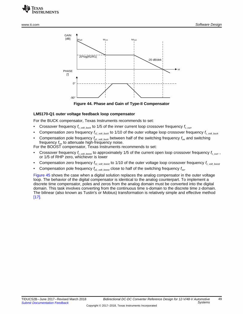
&
-90°
0°
&cz1 &Cp1&cp0
-20 dB/dek
GAIN [dB]
PHASE[°]
20*log(R2/R1)
www.ti.com Software Design
49TIDUCS2B–June 2017–Revised March 2018Submit Documentation Feedback
Copyright © 2017–2018, Texas Instruments Incorporated
Bidirectional DC-DC Converter Reference Design for 12-V/48-V AutomotiveSystems
Figure 44. Phase and Gain of Type-II Compensator
LM5170-Q1 outer voltage feedback loop compensatorFor the BUCK compensator, Texas Instruments recommends to set:• Crossover frequency fc_volt_buck to 1/5 of the inner current loop crossover frequency fc_curr
• Compensation zero frequency fz1_volt_buck to 1/10 of the outer voltage loop crossover frequency fc_volt_buck
• Compensation pole frequency fp1_volt_buck between half of the switching frequency fsw and switchingfrequency fsw to attenuate high-frequency noise.
For the BOOST compensator, Texas Instruments recommends to set:• Crossover frequency fc_volt_boost to approximately 1/5 of the current open loop crossover frequency fc_curr ,
or 1/5 of RHP zero, whichever is lower• Compensation zero frequency fz1_volt_boost to 1/10 of the outer voltage loop crossover frequency fc_volt_boost
• Compensation pole frequency fp1_volt_boost close to half of the switching frequency fsw.
Figure 45 shows the case when a digital solution replaces the analog compensator in the outer voltageloop. The behavior of the digital compensator is identical to the analog counterpart. To implement adiscrete time compensator, poles and zeros from the analog domain must be converted into the digitaldomain. This task involves converting from the continuous time s-domain to the discrete time z-domain.The bilinear (also known as Tustin's or Mobius) transformation is relatively simple and effective method[17].
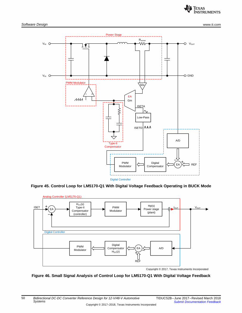
HCC(s)Type-II
Compensator (controller)
PWM Modulator
Hp(s)Power stage
(plant)EA
ISET VOUTIOUT
PWM Modulator
Digital Compensator
HDC(z)A/D
REF
Digital Controller
EA
Analog Controller (LM5170-Q1)
Copyright © 2017, Texas Instruments Incorporated
VIN
VIN
ISETA
+±
Power Stage
PWM Modulator
Type-II Compensator
EA
Rsense
Gm
50x
VOUT
GND
PWM Modulator
Digital Compensator
A/D
EA REF
Low-Pass
ISETD
Digital Controller
Software Design www.ti.com
50 TIDUCS2B–June 2017–Revised March 2018Submit Documentation Feedback
Copyright © 2017–2018, Texas Instruments Incorporated
Bidirectional DC-DC Converter Reference Design for 12-V/48-V AutomotiveSystems
Figure 45. Control Loop for LM5170-Q1 With Digital Voltage Feedback Operating in BUCK Mode
Figure 46. Small Signal Analysis of Control Loop for LM5170-Q1 With Digital Voltage Feedback

> @ > @ > @ > @ > @ > @ > @ > @
> @ > @ > @ > @ > @ > @
2 1 2 12 2 2 2 0
2 1 2 1 0
2 1 0 2 1
y z A z A z 1 x z B z B z B
A y n 2 A y n 1 y n B x n 2 B x n 1 B x n
y n B x n 2 B x n 1 B x n A y n 2 A y n 1
> @> @
> @
2 12 1 0
C 2 12 1
y z B z B z BH z
x z A z A z 1
cp0 cp1 CZ10
CP1 CZ1
2
1cp1
cp0 cp1 cz12
cp1 cz1
1cp1
cp12
cp1
T 2 TB
2 2 T
T cp0 cp1B
2 T
T 2 TB
2 2 T
4A
2 T
2 TA
2 T
Z
Z Z Z
Z Z
Z Z
Z
Z Z
Z Z
Z
Z
Z
> @2
2 1 0C 2
2 1
B B z B zH Z
A A z z
> @
cp02z 1 cz1
C
cp1
2z 1Tz 1
1
H Z2z 1Tz 1
Tz 11
Z
Z u
Z
2z 1s
Tz 1
m
www.ti.com Software Design
51TIDUCS2B–June 2017–Revised March 2018Submit Documentation Feedback
Copyright © 2017–2018, Texas Instruments Incorporated
Bidirectional DC-DC Converter Reference Design for 12-V/48-V AutomotiveSystems
The transfer function of an analog compensator can be converted in to the z-domain by replacing the 's'terms with:
(5)
where T is the sampling period tadc_ctrl_sampl. Equation 5 may then be substituted into the type-II controllertransfer function given in Equation 1 to yield the equivalent discrete time compensator transfer function inEquation 6.
(6)
After some algebraic manipulation, this function can be represented in terms of a standard discrete two-pole two-zero (2p2z) discrete controller transfer function (see Equation 7).
(7)
where,
(8)
To obtain the linear difference equation (LDE) from the two-pole two-zero discrete transfer function(Equation 7), first multiply both top and bottom through by z-2, as shown in Equation 9.
(9)
Equation 9 can now be rearranged to obtain the linear difference equation that can be calculated using amicroprocessor:
(10)
Where x[n] is the error input to the controller for this sampling period and y[n] is the controller output forthis sampling period. x[n-1] denotes the pervious sampling period and x[n-2] is two sampling periods in thepast.
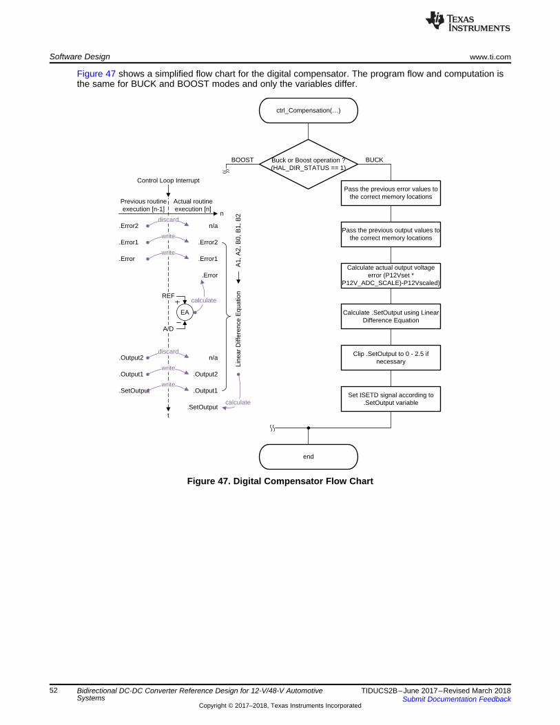
ctrl_Compensation(«)
Buck or Boost operation ?(HAL_DIR_STATUS == 1)
end
Pass the previous error values to the correct memory locations
BUCKBOOST
Pass the previous output values to the correct memory locations
Calculate actual output voltage error (P12Vset *
P12V_ADC_SCALE)-P12Vscaled)
Previous routine execution [n-1]
n
Actual routine execution [n]
.Error2
.Error1
.Error
.Error1
.Error
n/a.Error2
write
write
discard
A/D
REF
Control Loop Interrupt
calculate
EA
.Output1
.SetOutput
.Output2
.Output1
.SetOutput
.Output2
n/a
write
write
discard
t
Line
ar D
iffer
ence
Equ
atio
n
calculate
A1,
A2,
B0,
B1,
B2
Calculate .SetOutput using Linear Difference Equation
Clip .SetOutput to 0 - 2.5 if necessary
Set ISETD signal according to .SetOutput variable
Software Design www.ti.com
52 TIDUCS2B–June 2017–Revised March 2018Submit Documentation Feedback
Copyright © 2017–2018, Texas Instruments Incorporated
Bidirectional DC-DC Converter Reference Design for 12-V/48-V AutomotiveSystems
Figure 47 shows a simplified flow chart for the digital compensator. The program flow and computation isthe same for BUCK and BOOST modes and only the variables differ.
Figure 47. Digital Compensator Flow Chart
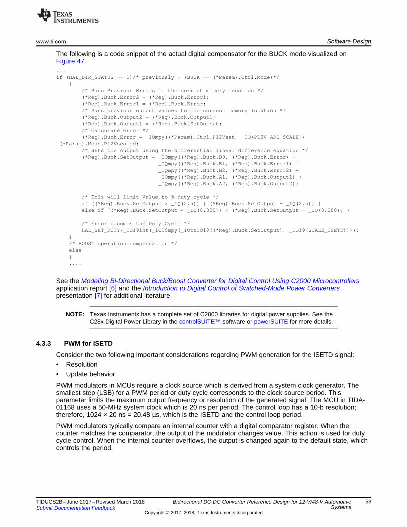
www.ti.com Software Design
53TIDUCS2B–June 2017–Revised March 2018Submit Documentation Feedback
Copyright © 2017–2018, Texas Instruments Incorporated
Bidirectional DC-DC Converter Reference Design for 12-V/48-V AutomotiveSystems
The following is a code snippet of the actual digital compensator for the BUCK mode visualized onFigure 47....if (HAL_DIR_STATUS == 1)/* previously = (BUCK == (*Param).Ctrl.Mode)*/
/* Pass Previous Errors to the correct memory location */(*Reg).Buck.Error2 = (*Reg).Buck.Error1;(*Reg).Buck.Error1 = (*Reg).Buck.Error;/* Pass previous output values to the correct memory location */(*Reg).Buck.Output2 = (*Reg).Buck.Output1;(*Reg).Buck.Output1 = (*Reg).Buck.SetOutput;/* Calculate error */(*Reg).Buck.Error = _IQmpy((*Param).Ctrl.P12Vset, _IQ(P12V_ADC_SCALE)) -
(*Param).Meas.P12Vscaled;/* Sets the output using the differential linear difference equation */(*Reg).Buck.SetOutput = _IQmpy((*Reg).Buck.B0, (*Reg).Buck.Error) +
_IQmpy((*Reg).Buck.B1, (*Reg).Buck.Error1) +_IQmpy((*Reg).Buck.B2, (*Reg).Buck.Error2) +_IQmpy((*Reg).Buck.A1, (*Reg).Buck.Output1) +_IQmpy((*Reg).Buck.A2, (*Reg).Buck.Output2);
/* This will limit Value to % duty cycle */if ((*Reg).Buck.SetOutput > _IQ(2.5)) (*Reg).Buck.SetOutput = _IQ(2.5); else if ((*Reg).Buck.SetOutput < _IQ(0.000)) (*Reg).Buck.SetOutput = _IQ(0.000);
/* Error becomes the Duty Cycle */HAL_SET_DUTY(_IQ19int(_IQ19mpy(_IQtoIQ19((*Reg).Buck.SetOutput), _IQ19(SCALE_ISETD))));
/* BOOST operation compensation */else....
See the Modeling Bi-Directional Buck/Boost Converter for Digital Control Using C2000 Microcontrollersapplication report [6] and the Introduction to Digital Control of Switched-Mode Power Converterspresentation [7] for additional literature.
NOTE: Texas Instruments has a complete set of C2000 libraries for digital power supplies. See theC28x Digital Power Library in the controlSUITE™ software or powerSUITE for more details.
4.3.3 PWM for ISETDConsider the two following important considerations regarding PWM generation for the ISETD signal:• Resolution• Update behavior
PWM modulators in MCUs require a clock source which is derived from a system clock generator. Thesmallest step (LSB) for a PWM period or duty cycle corresponds to the clock source period. Thisparameter limits the maximum output frequency or resolution of the generated signal. The MCU in TIDA-01168 uses a 50-MHz system clock which is 20 ns per period. The control loop has a 10-b resolution;therefore, 1024 × 20 ns = 20.48 µs, which is the ISETD and the control loop period.
PWM modulators typically compare an internal counter with a digital comparator register. When thecounter matches the comparator, the output of the modulator changes value. This action is used for dutycycle control. When the internal counter overflows, the output is changed again to the default state, whichcontrols the period.
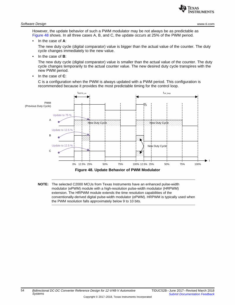
PWM (Previous Duty Cycle)
A
B
C
t
New Duty CycleNew Duty Cycle
12.5%0%
tISETD_on tctrl_loop
25% 50% 75% 100% 12.5% 25% 50% 75% 100%
New Duty CycleUpdate to 12.5 %
Update to 12.5 %
Update to 75 %
Software Design www.ti.com
54 TIDUCS2B–June 2017–Revised March 2018Submit Documentation Feedback
Copyright © 2017–2018, Texas Instruments Incorporated
Bidirectional DC-DC Converter Reference Design for 12-V/48-V AutomotiveSystems
However, the update behavior of such a PWM modulator may be not always be as predictable asFigure 48 shows. In all three cases A, B, and C, the update occurs at 25% of the PWM period.• In the case of A:
The new duty cycle (digital comparator) value is bigger than the actual value of the counter. The dutycycle changes immediately to the new value.
• In the case of B:The new duty cycle (digital comparator) value is smaller than the actual value of the counter. The dutycycle changes temporarily to the actual counter value. The new desired duty cycle transpires with thenew PWM period.
• In the case of C:C is a configuration when the PWM is always updated with a PWM period. This configuration isrecommended because it provides the most predictable timing for the control loop.
Figure 48. Update Behavior of PWM Modulator
NOTE: The selected C2000 MCUs from Texas Instruments have an enhanced pulse-widthmodulator (ePWM) module with a high-resolution pulse-width modulator (HRPWM)extension. The HRPWM module extends the time resolution capabilities of theconventionally-derived digital pulse-width modulator (ePWM). HRPWM is typically used whenthe PWM resolution falls approximately below 9 to 10 bits.

Electronic Load
+
±
48 V Power Supply
20 A
10 A
10 A
Delivering 10 A to the system
Sinking 10 A from the system
10 A
0 A 10 A
DC / DCElectronic Load
+
±
48 V Power Supply
KL40
KL41
KL30
KL31
Electronic Load
+
±
12 V Power Supply
V48
VI48
V12
VI12
Host System
JTAG / UART / SPI / I2C
EN
12
EN
48
BU
S
RSHUNT48 RSHUNT12
www.ti.com Getting Started Hardware and Software
55TIDUCS2B–June 2017–Revised March 2018Submit Documentation Feedback
Copyright © 2017–2018, Texas Instruments Incorporated
Bidirectional DC-DC Converter Reference Design for 12-V/48-V AutomotiveSystems
5 Getting Started Hardware and Software
5.1 Hardware
5.1.1 Recommended Laboratory Setup DescriptionA test setup for a bidirectional DC-DC converter is quite complex. Figure 49 shows a recommendedhardware setup for TIDA-01168.
Figure 49. Recommended Hardware Setup for TIDA-01168
Power supplies on both sides must be able to source and sink current (two-quadrant power supply) incases where bidirectional operation is desired. Alternatively, a traditional one-quadrant power supply canbe used in parallel with an electronic load for the replacement (see Figure 50). The power supply currentlimit corresponds to the sum of input and output currents from the system. The electronic load operates inconstant current mode set to the level of maximum output current from the system. When the systemoperates as a load, the energy consumed by the electronic load is wasted. When the system operates asa source then the electronic load consumes all current and adds all the current from the 48-V powersupply on top to achieve the preset value. See the LM5170-Q1 EVM User Guide [8] for further information.
Figure 50. Power Supply With Electronic Load in Parallel Allowing Bidirectional Current Flow
NOTE: The digital voltage control implemented in TIDA-01168 does not have a current limit. Thevoltage feedback loop must be disabled when using a power supply in parallel with anelectronic load, such as in the example shown in Figure 50.

Getting Started Hardware and Software www.ti.com
56 TIDUCS2B–June 2017–Revised March 2018Submit Documentation Feedback
Copyright © 2017–2018, Texas Instruments Incorporated
Bidirectional DC-DC Converter Reference Design for 12-V/48-V AutomotiveSystems
High currents on power rails are measured indirectly by measuring the voltage (VI12, VI48) across aprecision shunt resistor (RSHUNT12, RSHUNT48). Figure 52 shows an example of these precision resistors. Thepower rail voltage is measured directly on KL30, KL31 and KL40, and KL41 system terminals. Terminalswith cable lugs are modified as shown in Figure 51 to fit the mechanical dimensions of the PCB thesystem. The host system is a battery-operated laptop which controls the TIDA-01168 using a JTAG oruniversal asynchronous receiver/transmitter (UART) interface. The EN12 and EN48 enable signals comefrom an additional laboratory power supply.
Figure 51. Modified Terminals for TIDA-01168 Figure 52. Current Shunts
See Table 15 for an overview of the selected hardware used during TIDA-01168 development.
Table 15. List of Equipment Used for Test Setup
EQUIPMENT TYPE48-V power supply Chroma 62024P-80-6048-V electronic load BK Precision 851812-V power supply Supply Chroma 62012P-40-12048-V electronic load Kikusui PLZ10004WV48, V12 Voltmeters Fluke 87-V Industrial Multimeter
VI48, VI12 Voltmeters Keysight 34410ARSHUNT48 Murata Power Solutions 3020-01108-0RSHUNT12 Murata Power Solutions 3020-01101-0
JTAG probe XDS100v2 JTAG Debug Probe (14-pin TI version)(TMDSEMU100V2U-14)
Cables AWG8, AWG6
KL40, KL41, KL30, KL31 terminalsPanduitCB70-14-CY (image of modified version in Figure 51)
www.ti.com Getting Started Hardware and Software
57TIDUCS2B–June 2017–Revised March 2018Submit Documentation Feedback
Copyright © 2017–2018, Texas Instruments Incorporated
Bidirectional DC-DC Converter Reference Design for 12-V/48-V AutomotiveSystems
5.2 TIDA-01168 First PoweringThis subsection describes a concise, step-by-step procedure for the turnon required by the TIDA-01168for MCU programming.
Follow these steps when first powering the reference design in BUCK mode (unidirectional operation):1. Make sure to switch off all the laboratory equipment (laboratory power supplies, for example).2. Connect the 48-V power supply output to KL40 (positive) and KL41 (negative) terminals. Preset the
output voltage to 48 V and set the current limit to 1 A.3. Connect signal EN48 (J702, pin 6) and ground (J702, pin 4) to an external laboratory power supply.
Preset the output voltage to 5 V and set the current limit to 10 mA. Keep the output OFF.4. Connect the XDS100 JTAG probe to J800.5. Connect the JTAG probe to the laptop.6. Turn on the 48-V power supply.7. Turn on the external laboratory power supply for the EN48.8. Verify that the LEDs are ON.9. Proceed to the software section.
5.3 SoftwareThe MCU in the TIDA-01168 reference design must be programmed to make the system functional. TIrecommends using the JTAG programming interface.
NOTE: The software configuration in the following subsections utilize the Microsoft® Windows® 7operating system SP1 (x64), build 7601 and a Google Chrome™ browser (56.0.2924.87).
5.3.1 JTAG Probe ConfigurationProgramming the TMS320F28027F MCU in the TIDA-01168 design requires a C2000-compatible JTAGprobe. Texas Instruments recommends the ultra-low-cost XDS100V2. The driver for the XDS100v2 JTAGprobe is a part of various Texas Instruments software packages:• Code Composer Studio (complete development toolchain)• Uniflash• controlSUITE• TI Cloud Agent (internet browser extension for TI Cloud Tools)
Install one of these applications if the Windows operating system prompts for a driver. Figure 53 shows ascreenshot of the Device Manager confirming a properly installed XDS100v2 driver. Make sure that thevirtual COM port (VCP) box is checked for both channels as Figure 54 shows.
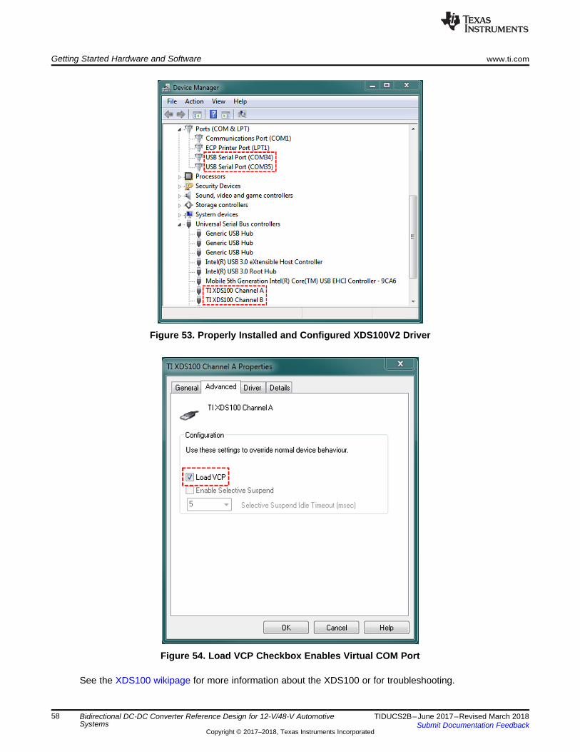
Getting Started Hardware and Software www.ti.com
58 TIDUCS2B–June 2017–Revised March 2018Submit Documentation Feedback
Copyright © 2017–2018, Texas Instruments Incorporated
Bidirectional DC-DC Converter Reference Design for 12-V/48-V AutomotiveSystems
Figure 53. Properly Installed and Configured XDS100V2 Driver
Figure 54. Load VCP Checkbox Enables Virtual COM Port
See the XDS100 wikipage for more information about the XDS100 or for troubleshooting.
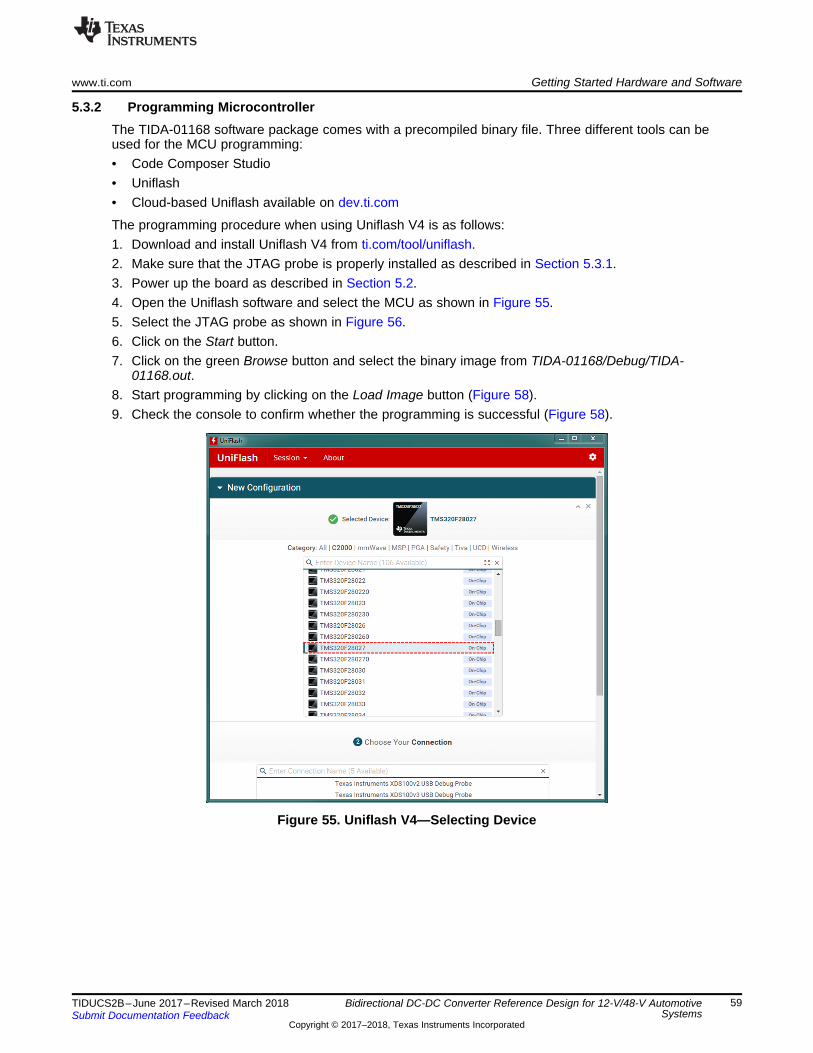
www.ti.com Getting Started Hardware and Software
59TIDUCS2B–June 2017–Revised March 2018Submit Documentation Feedback
Copyright © 2017–2018, Texas Instruments Incorporated
Bidirectional DC-DC Converter Reference Design for 12-V/48-V AutomotiveSystems
5.3.2 Programming MicrocontrollerThe TIDA-01168 software package comes with a precompiled binary file. Three different tools can beused for the MCU programming:• Code Composer Studio• Uniflash• Cloud-based Uniflash available on dev.ti.com
The programming procedure when using Uniflash V4 is as follows:1. Download and install Uniflash V4 from ti.com/tool/uniflash.2. Make sure that the JTAG probe is properly installed as described in Section 5.3.1.3. Power up the board as described in Section 5.2.4. Open the Uniflash software and select the MCU as shown in Figure 55.5. Select the JTAG probe as shown in Figure 56.6. Click on the Start button.7. Click on the green Browse button and select the binary image from TIDA-01168/Debug/TIDA-
01168.out.8. Start programming by clicking on the Load Image button (Figure 58).9. Check the console to confirm whether the programming is successful (Figure 58).
Figure 55. Uniflash V4—Selecting Device
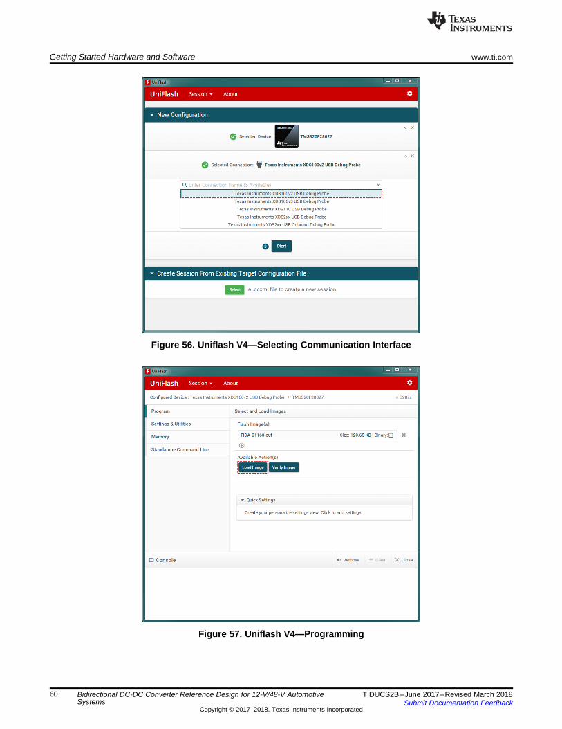
Getting Started Hardware and Software www.ti.com
60 TIDUCS2B–June 2017–Revised March 2018Submit Documentation Feedback
Copyright © 2017–2018, Texas Instruments Incorporated
Bidirectional DC-DC Converter Reference Design for 12-V/48-V AutomotiveSystems
Figure 56. Uniflash V4—Selecting Communication Interface
Figure 57. Uniflash V4—Programming

www.ti.com Getting Started Hardware and Software
61TIDUCS2B–June 2017–Revised March 2018Submit Documentation Feedback
Copyright © 2017–2018, Texas Instruments Incorporated
Bidirectional DC-DC Converter Reference Design for 12-V/48-V AutomotiveSystems
Figure 58. Uniflash V4—Programming Finished
NOTE: For more information on how to modify or compile a provided source code using C2000Compiler and Code Composer Studio visit processors.wiki.ti.com or ask on the TI E2E™online community.
5.3.3 Using Software for TIDA-01168The following two options are available for configuring and controlling the TIDA-01168:• GUI Composer application (JTAG)• Serial terminal (UART)
5.3.3.1 Using GUI ComposerGUI Composer is a cloud-based graphic user interface available on dev.ti.com. The tool uses non-intrusive JTAG access to read and write data to the MCU. System variables are displayed in the Internetbrowser. Google Chrome™ or Mozilla® Firefox® are the supported browsers with an additional plugin (TICloud Agent Bridge). Any additional communication protocol is not necessary. The user can import theproject from the gallery to their workspace or download a standalone version available for variousoperating systems. The GUI Composer project contains the binary file and, if set properly, the fileeliminates the process of programming the MCU as described in Section 5.3.2. The GUI Composer canprogram the MCU either every run or upon request from the menu.
NOTE: The GUI Composer application is easy to use but is considered to be experimental. Userexperience depends on several factors such as Internet service provider (ISP) bandwidth,Internet browser, or PC hardware. TI provides absolutely no warranty for using the software.
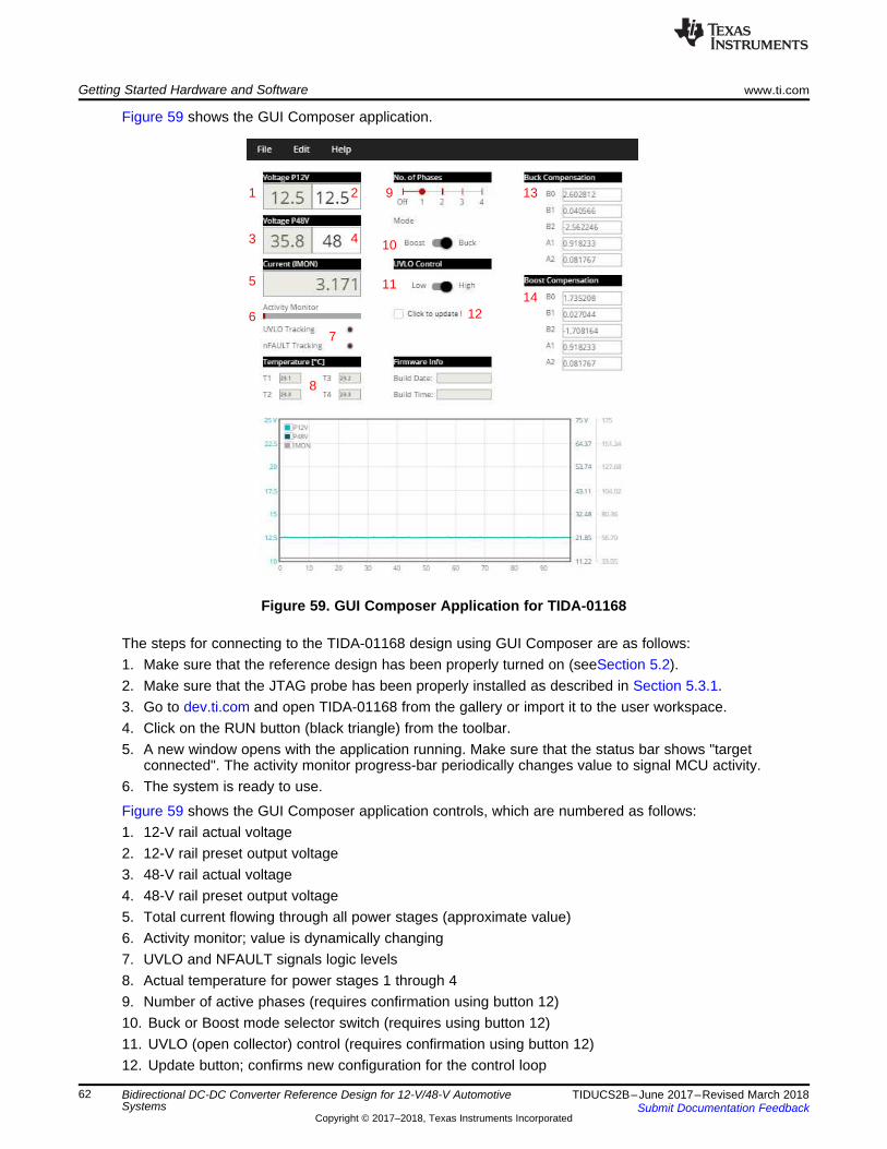
1 2
3 4
5
6
7
8
9
10
11
12
13
14
Getting Started Hardware and Software www.ti.com
62 TIDUCS2B–June 2017–Revised March 2018Submit Documentation Feedback
Copyright © 2017–2018, Texas Instruments Incorporated
Bidirectional DC-DC Converter Reference Design for 12-V/48-V AutomotiveSystems
Figure 59 shows the GUI Composer application.
Figure 59. GUI Composer Application for TIDA-01168
The steps for connecting to the TIDA-01168 design using GUI Composer are as follows:1. Make sure that the reference design has been properly turned on (seeSection 5.2).2. Make sure that the JTAG probe has been properly installed as described in Section 5.3.1.3. Go to dev.ti.com and open TIDA-01168 from the gallery or import it to the user workspace.4. Click on the RUN button (black triangle) from the toolbar.5. A new window opens with the application running. Make sure that the status bar shows "target
connected". The activity monitor progress-bar periodically changes value to signal MCU activity.6. The system is ready to use.
Figure 59 shows the GUI Composer application controls, which are numbered as follows:1. 12-V rail actual voltage2. 12-V rail preset output voltage3. 48-V rail actual voltage4. 48-V rail preset output voltage5. Total current flowing through all power stages (approximate value)6. Activity monitor; value is dynamically changing7. UVLO and NFAULT signals logic levels8. Actual temperature for power stages 1 through 49. Number of active phases (requires confirmation using button 12)10. Buck or Boost mode selector switch (requires using button 12)11. UVLO (open collector) control (requires confirmation using button 12)12. Update button; confirms new configuration for the control loop
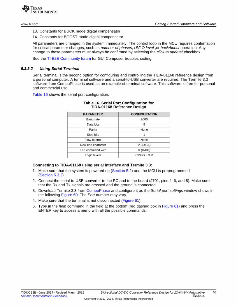
www.ti.com Getting Started Hardware and Software
63TIDUCS2B–June 2017–Revised March 2018Submit Documentation Feedback
Copyright © 2017–2018, Texas Instruments Incorporated
Bidirectional DC-DC Converter Reference Design for 12-V/48-V AutomotiveSystems
13. Constants for BUCK mode digital compensator14. Constants for BOOST mode digital compensator
All parameters are changed in the system immediately. The control loop in the MCU requires confirmationfor critical parameter changes, such as number of phases, UVLO level ,or buck/boost operation. Anychange to these parameters must always be confirmed by selecting the click to update! checkbox.
See the TI E2E Community forum for GUI Composer troubleshooting.
5.3.3.2 Using Serial TerminalSerial terminal is the second option for configuring and controlling the TIDA-01168 reference design froma personal computer. A terminal software and a serial-to-USB converter are required. The Termite 3.3software from CompuPhase is used as an example of terminal software. This software is free for personaland commercial use.
Table 16 shows the serial port configuration.
Table 16. Serial Port Configuration forTIDA-01168 Reference Design
PARAMETER CONFIGURATIONBaud rate 9600Data bits 8
Parity NoneStop bits 1
Flow control NoneNew line character \n (0x0A)End command with \r (0x0D)
Logic levels CMOS 3.3 V
Connecting to TIDA-01168 using serial interface and Termite 3.3:1. Make sure that the system is powered up (Section 5.2) and the MCU is preprogrammed
(Section 5.3.2).2. Connect the serial-to-USB converter to the PC and to the board (J701, pins 4, 6, and 8). Make sure
that the Rx and Tx signals are crossed and the ground is connected.3. Download Termite 3.3 from CompuPhase and configure it as the Serial port settings window shows in
the following Figure 60. The Port number may vary.4. Make sure that the terminal is not disconnected (Figure 61).5. Type in the help command in the field at the bottom (red dashed box in Figure 61) and press the
ENTER key to access a menu with all the possible commands.
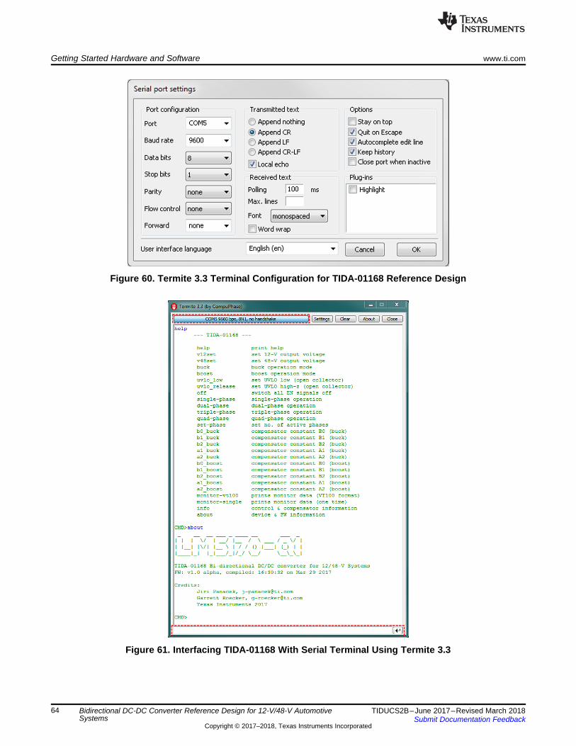
Getting Started Hardware and Software www.ti.com
64 TIDUCS2B–June 2017–Revised March 2018Submit Documentation Feedback
Copyright © 2017–2018, Texas Instruments Incorporated
Bidirectional DC-DC Converter Reference Design for 12-V/48-V AutomotiveSystems
Figure 60. Termite 3.3 Terminal Configuration for TIDA-01168 Reference Design
Figure 61. Interfacing TIDA-01168 With Serial Terminal Using Termite 3.3
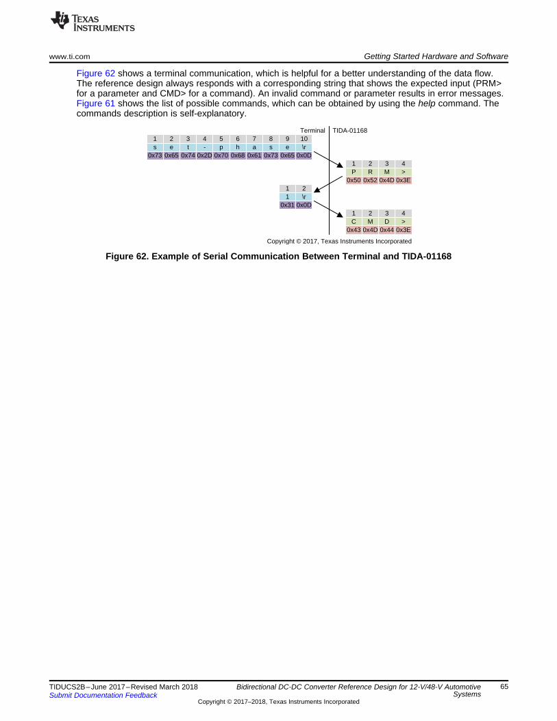
1P
0x50
2R
0x52
3M
0x4D
4>
0x3E
1C
0x43
2M
0x4D
3D
0x44
4>
0x3E
1s
0x73
2e
0x65
3t
0x74
4-
0x2D
5p
0x70
6h
0x68
7a
0x61
8s
0x73
9e
0x65
10\r
0x0D
11
0x31
2\r
0x0D
Terminal TIDA-01168
Copyright © 2017, Texas Instruments Incorporated
www.ti.com Getting Started Hardware and Software
65TIDUCS2B–June 2017–Revised March 2018Submit Documentation Feedback
Copyright © 2017–2018, Texas Instruments Incorporated
Bidirectional DC-DC Converter Reference Design for 12-V/48-V AutomotiveSystems
Figure 62 shows a terminal communication, which is helpful for a better understanding of the data flow.The reference design always responds with a corresponding string that shows the expected input (PRM>for a parameter and CMD> for a command). An invalid command or parameter results in error messages.Figure 61 shows the list of possible commands, which can be obtained by using the help command. Thecommands description is self-explanatory.
Figure 62. Example of Serial Communication Between Terminal and TIDA-01168
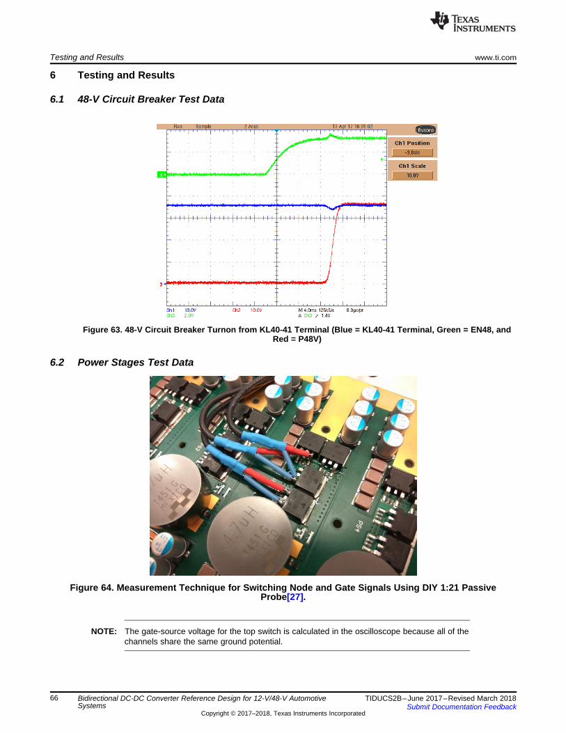
Testing and Results www.ti.com
66 TIDUCS2B–June 2017–Revised March 2018Submit Documentation Feedback
Copyright © 2017–2018, Texas Instruments Incorporated
Bidirectional DC-DC Converter Reference Design for 12-V/48-V AutomotiveSystems
6 Testing and Results
6.1 48-V Circuit Breaker Test Data
Figure 63. 48-V Circuit Breaker Turnon from KL40-41 Terminal (Blue = KL40-41 Terminal, Green = EN48, andRed = P48V)
6.2 Power Stages Test Data
Figure 64. Measurement Technique for Switching Node and Gate Signals Using DIY 1:21 PassiveProbe[27].
NOTE: The gate-source voltage for the top switch is calculated in the oscilloscope because all of thechannels share the same ground potential.
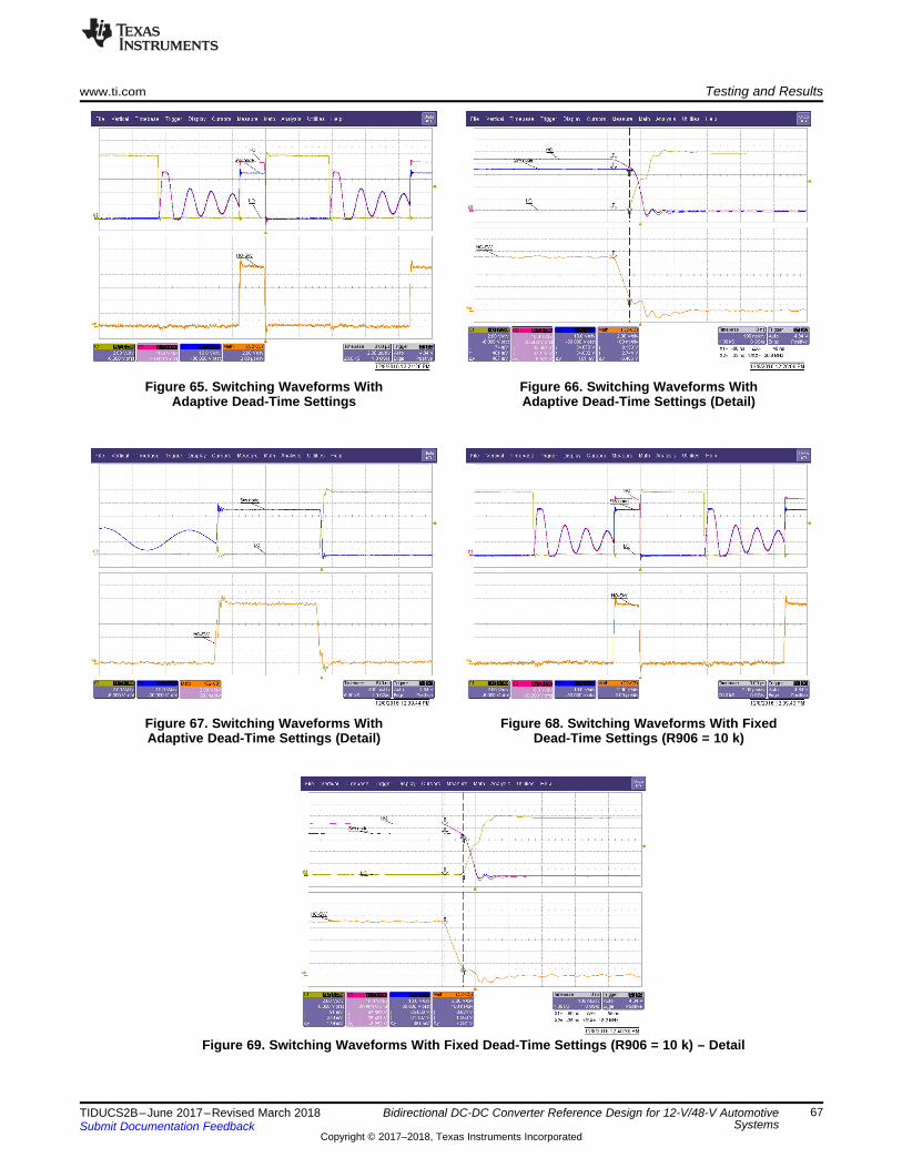
www.ti.com Testing and Results
67TIDUCS2B–June 2017–Revised March 2018Submit Documentation Feedback
Copyright © 2017–2018, Texas Instruments Incorporated
Bidirectional DC-DC Converter Reference Design for 12-V/48-V AutomotiveSystems
Figure 65. Switching Waveforms WithAdaptive Dead-Time Settings
Figure 66. Switching Waveforms WithAdaptive Dead-Time Settings (Detail)
Figure 67. Switching Waveforms WithAdaptive Dead-Time Settings (Detail)
Figure 68. Switching Waveforms With FixedDead-Time Settings (R906 = 10 k)
Figure 69. Switching Waveforms With Fixed Dead-Time Settings (R906 = 10 k) – Detail

Testing and Results www.ti.com
68 TIDUCS2B–June 2017–Revised March 2018Submit Documentation Feedback
Copyright © 2017–2018, Texas Instruments Incorporated
Bidirectional DC-DC Converter Reference Design for 12-V/48-V AutomotiveSystems
6.3 12-V Circuit Breaker Test Data
Figure 70. 12-V Circuit Breaker Turnon From 12-VTerminal (Green = UVLO, Red = P12V)
Figure 71. 12-V Circuit Breaker Turnon to 12-V Terminal(Blue = KL30-31 Terminal, Green = UVLO,
and Red = P12V)
Figure 72. 12-V Circuit Breaker Turnoff From 12-VTerminal (Green = UVLO, Red = P12V)
Figure 73. 12-V Circuit Breaker Turnoff to 12-V Terminal(Blue = KL30-31 Terminal, Green = UVLO,
and Red = P12V)
ISETD Duty
ISE
TA
(V
)
0.1% 0.2% 0.3% 0.4% 0.5% 0.6% 0.7% 0.8% 0.9% 1%0.3
0.6
0.9
1.2
1.5
1.8
2.1
2.4
2.7
3.0
3.3
D004
www.ti.com Testing and Results
69TIDUCS2B–June 2017–Revised March 2018Submit Documentation Feedback
Copyright © 2017–2018, Texas Instruments Incorporated
Bidirectional DC-DC Converter Reference Design for 12-V/48-V AutomotiveSystems
6.4 LM5170-Q1 Subsystem Test Data
Figure 74. Relationship Between ISETD Duty Cycle and ISETA Voltage: C912 = 3.3 nF, fISED = 48.8 kHz
6.5 C2000™ Control MCU Test Data
Figure 75. Timing of Control loop ISR Measured onTestpin ADCINB2 (D700)
Figure 76. I2C Bus TMP102-Q1 Frames Timing
Figure 77. I 2 C Bus TMP102-Q1 Single Frame Timing Figure 78. I 2 C Bus TMP102-Q1 Single Frame Timing(Detail)
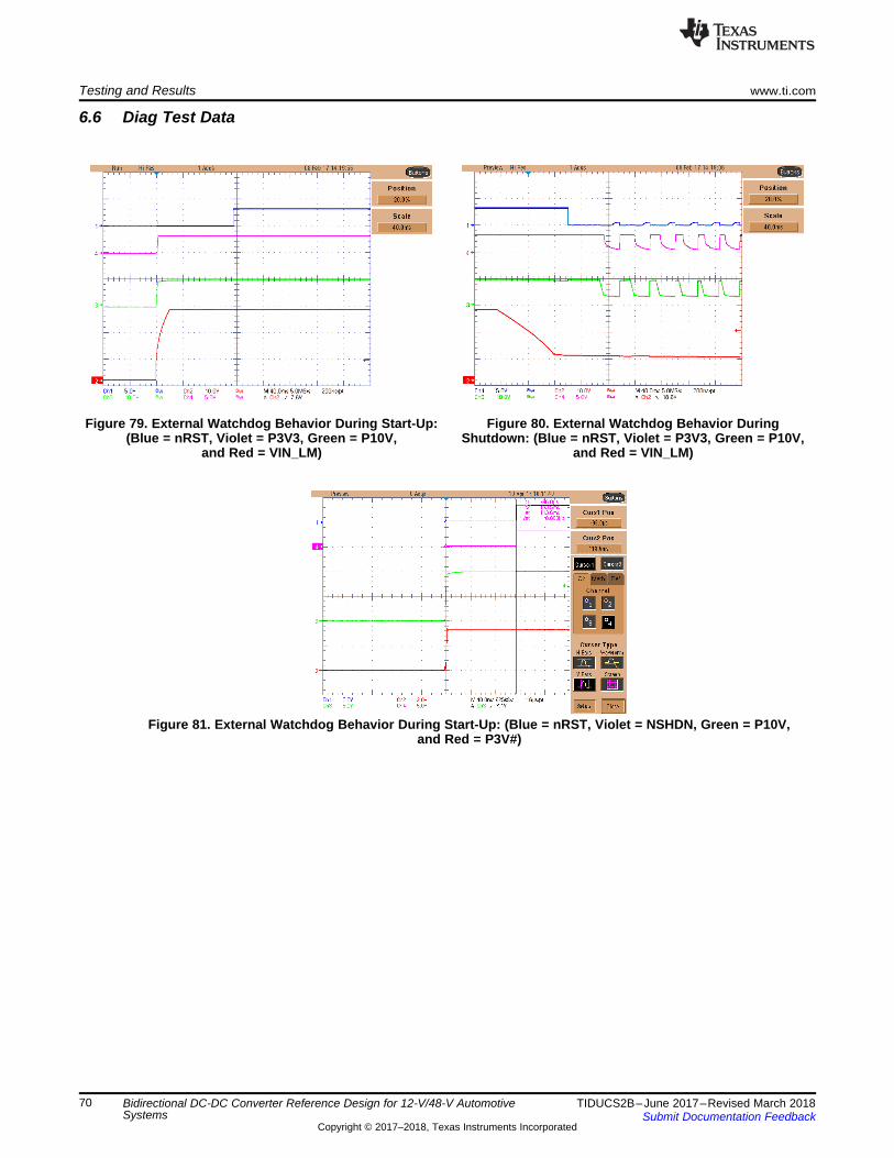
Testing and Results www.ti.com
70 TIDUCS2B–June 2017–Revised March 2018Submit Documentation Feedback
Copyright © 2017–2018, Texas Instruments Incorporated
Bidirectional DC-DC Converter Reference Design for 12-V/48-V AutomotiveSystems
6.6 Diag Test Data
Figure 79. External Watchdog Behavior During Start-Up:(Blue = nRST, Violet = P3V3, Green = P10V,
and Red = VIN_LM)
Figure 80. External Watchdog Behavior DuringShutdown: (Blue = nRST, Violet = P3V3, Green = P10V,
and Red = VIN_LM)
Figure 81. External Watchdog Behavior During Start-Up: (Blue = nRST, Violet = NSHDN, Green = P10V,and Red = P3V#)
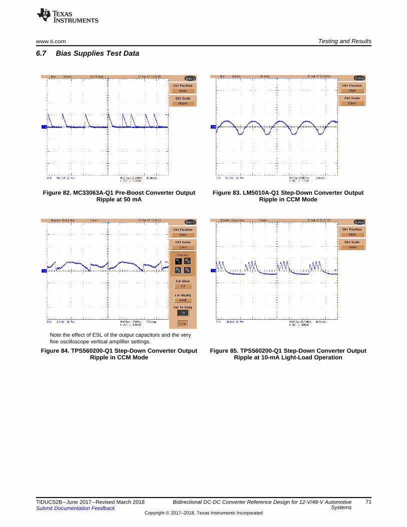
www.ti.com Testing and Results
71TIDUCS2B–June 2017–Revised March 2018Submit Documentation Feedback
Copyright © 2017–2018, Texas Instruments Incorporated
Bidirectional DC-DC Converter Reference Design for 12-V/48-V AutomotiveSystems
6.7 Bias Supplies Test Data
Figure 82. MC33063A-Q1 Pre-Boost Converter OutputRipple at 50 mA
Figure 83. LM5010A-Q1 Step-Down Converter OutputRipple in CCM Mode
Note the effect of ESL of the output capacitors and the veryfine oscilloscope vertical amplifier settings.
Figure 84. TPS560200-Q1 Step-Down Converter OutputRipple in CCM Mode
Figure 85. TPS560200-Q1 Step-Down Converter OutputRipple at 10-mA Light-Load Operation
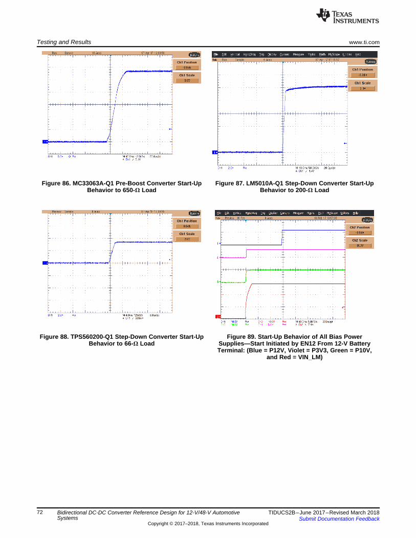
Testing and Results www.ti.com
72 TIDUCS2B–June 2017–Revised March 2018Submit Documentation Feedback
Copyright © 2017–2018, Texas Instruments Incorporated
Bidirectional DC-DC Converter Reference Design for 12-V/48-V AutomotiveSystems
Figure 86. MC33063A-Q1 Pre-Boost Converter Start-UpBehavior to 650-Ω Load
Figure 87. LM5010A-Q1 Step-Down Converter Start-UpBehavior to 200-Ω Load
Figure 88. TPS560200-Q1 Step-Down Converter Start-UpBehavior to 66-Ω Load
Figure 89. Start-Up Behavior of All Bias PowerSupplies—Start Initiated by EN12 From 12-V BatteryTerminal: (Blue = P12V, Violet = P3V3, Green = P10V,
and Red = VIN_LM)
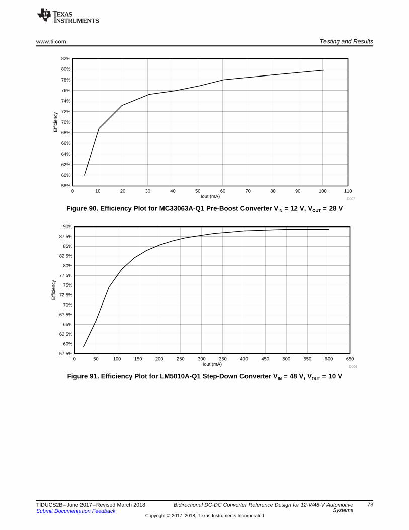
Iout (mA)
Effi
cien
cy
0 50 100 150 200 250 300 350 400 450 500 550 600 65057.5%
60%
62.5%
65%
67.5%
70%
72.5%
75%
77.5%
80%
82.5%
85%
87.5%
90%
D006
Iout (mA)
Effi
cien
cy
0 10 20 30 40 50 60 70 80 90 100 11058%
60%
62%
64%
66%
68%
70%
72%
74%
76%
78%
80%
82%
D007
www.ti.com Testing and Results
73TIDUCS2B–June 2017–Revised March 2018Submit Documentation Feedback
Copyright © 2017–2018, Texas Instruments Incorporated
Bidirectional DC-DC Converter Reference Design for 12-V/48-V AutomotiveSystems
Figure 90. Efficiency Plot for MC33063A-Q1 Pre-Boost Converter VIN = 12 V, VOUT = 28 V
Figure 91. Efficiency Plot for LM5010A-Q1 Step-Down Converter VIN = 48 V, VOUT = 10 V
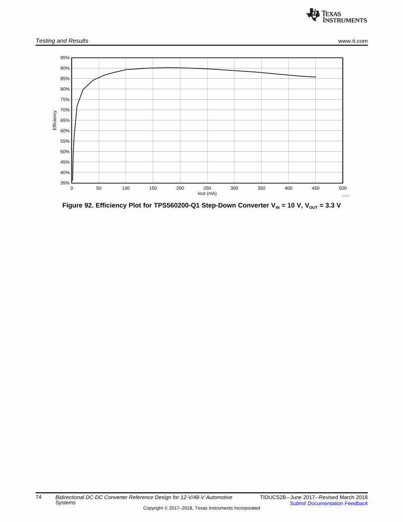
Iout (mA)
Effi
cien
cy
0 50 100 150 200 250 300 350 400 450 50035%
40%
45%
50%
55%
60%
65%
70%
75%
80%
85%
90%
95%
D005
Testing and Results www.ti.com
74 TIDUCS2B–June 2017–Revised March 2018Submit Documentation Feedback
Copyright © 2017–2018, Texas Instruments Incorporated
Bidirectional DC-DC Converter Reference Design for 12-V/48-V AutomotiveSystems
Figure 92. Efficiency Plot for TPS560200-Q1 Step-Down Converter VIN = 10 V, VOUT = 3.3 V
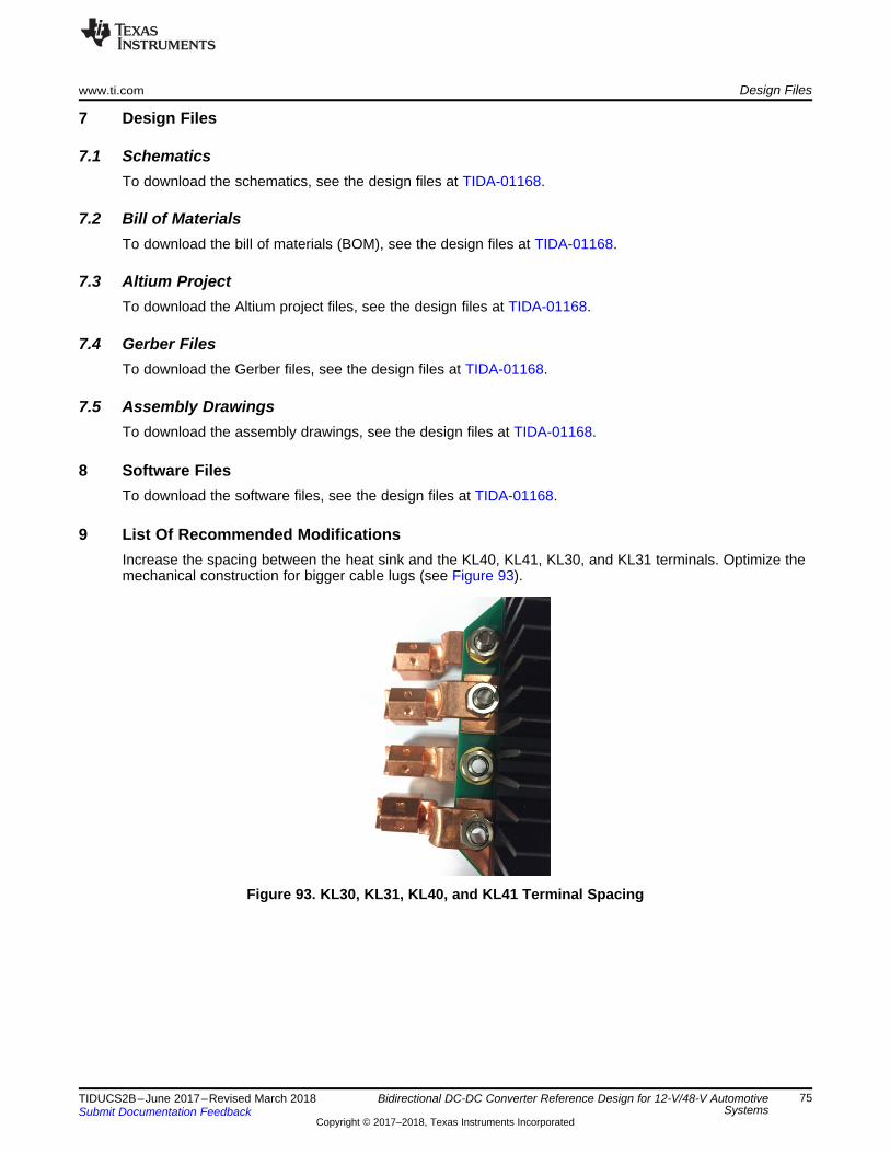
www.ti.com Design Files
75TIDUCS2B–June 2017–Revised March 2018Submit Documentation Feedback
Copyright © 2017–2018, Texas Instruments Incorporated
Bidirectional DC-DC Converter Reference Design for 12-V/48-V AutomotiveSystems
7 Design Files
7.1 SchematicsTo download the schematics, see the design files at TIDA-01168.
7.2 Bill of MaterialsTo download the bill of materials (BOM), see the design files at TIDA-01168.
7.3 Altium ProjectTo download the Altium project files, see the design files at TIDA-01168.
7.4 Gerber FilesTo download the Gerber files, see the design files at TIDA-01168.
7.5 Assembly DrawingsTo download the assembly drawings, see the design files at TIDA-01168.
8 Software FilesTo download the software files, see the design files at TIDA-01168.
9 List Of Recommended ModificationsIncrease the spacing between the heat sink and the KL40, KL41, KL30, and KL31 terminals. Optimize themechanical construction for bigger cable lugs (see Figure 93).
Figure 93. KL30, KL31, KL40, and KL41 Terminal Spacing
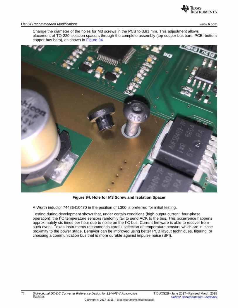
List Of Recommended Modifications www.ti.com
76 TIDUCS2B–June 2017–Revised March 2018Submit Documentation Feedback
Copyright © 2017–2018, Texas Instruments Incorporated
Bidirectional DC-DC Converter Reference Design for 12-V/48-V AutomotiveSystems
Change the diameter of the holes for M3 screws in the PCB to 3.81 mm. This adjustment allowsplacement of TO-220 isolation spacers through the complete assembly (top copper bus bars, PCB, bottomcopper bus bars), as shown in Figure 94.
Figure 94. Hole for M3 Screw and Isolation Spacer
A Wurth inductor 74436410470 in the position of L300 is preferred for initial testing.
Testing during development shows that, under certain conditions (high output current, four-phaseoperation), the I2C temperature sensors randomly fail to send ACK to the bus. This occurrence happensapproximately six times per hour due to noise on the I2C bus. Current firmware is able to recover fromsuch event. Texas Instruments recommends careful selection of temperature sensors which are in closeproximity to the power stage. Behavior can be improved using better PCB layout techniques, filtering, orchoosing a communication bus that is more durable against impulse noise (SPI).
www.ti.com Related Documentation
77TIDUCS2B–June 2017–Revised March 2018Submit Documentation Feedback
Copyright © 2017–2018, Texas Instruments Incorporated
Bidirectional DC-DC Converter Reference Design for 12-V/48-V AutomotiveSystems
10 Related Documentation1. Texas Instruments, 48V systems: Design considerations for a typical auxiliary power inverter, TI E2E™
Online Community Forum – Behind the Wheel; July 2015(https://e2e.ti.com/blogs_/b/behind_the_wheel/archive/2015/07/08/48v-systems-design-considerations-for-a-typical-auxiliary-power-inverter)
2. Texas Instruments, LM5170-Q1 Multiphase Bidirectional Current Controller, LM5170-Q1 Data Sheet(SNVSAQ6)
3. Forsythe, J.B.; Paralleling of Power MOSFETs, IEEE-IAS Conference Record, October 19814. Texas Instruments, LM5010A, LM5010A-Q1 High-Voltage 1-A Step-Down Switching Regulator,
LM5010A/LM5010A-Q1 Data Sheet (SNVS376)5. Texas Instruments, C28x IQmath Library, Software Module User's Guide (SPRC990)6. Texas Instruments, Modeling Bi-Directional Buck/Boost Converter for Digital Control Using C2000
Microcontrollers, Application Report (SPRABX5)7. University of Colorado, Introduction to Digital Control of Switched-Mode Power Converters, ECEN5807
Materials (http://ecee.colorado.edu/~ecen5807/course_material/digital/5807_Digital_Intro.pdf)8. Texas Instruments, LM5170-Q1 EVM User Guide, LM5170-Q1 EVM User's Guide (SNVU543)9. Environmental Protection Agency, Average Annual Emissions and Fuel Consumption for Gasoline-
Fueled Passenger Cars and Light Trucks, EPA420-F-08-024, October 2008 (https://nepis.epa.gov)10. European Commission, Reducing CO2 emissions from passenger cars, Climate Action Report
(https://ec.europa.eu/clima/policies/transport/vehicles/cars_en)11. Verband der Automobilindustrie e. V., Electric and Electronic Components in Motor Vehicles 48 V On-
Board Power Supply Requirements and Tests, VDA-320 Publication12. EETimes.com; Hegarty, Tim; Benefits of multiphasing buck converters (Part 1, Part 2), EE Times
Design How-To, 2007 (http://www.eetimes.com/document.asp?doc_id=1273224)13. EDN.com; Hegarty, Tim; Voltage-mode control and compensation: Intricacies for buck regulators,
EDN Network How To Article, 2008 (http://www.edn.com/design/analog/4326882/Voltage-mode-control-and-compensation-Intricacies-for-buck-regulators)
14. Ahonen, Janne, A wideband 1:21 DIY 1 kΩ oscilloscope probe, Online Publication(http://jahonen.kapsi.fi/Electronics/DIY%201k%20probe/)
15. Biricha DigitalPower Ltd, Designing Stable Digital Power Supplies, Seminar Presentation, 2011(https://www.omicron-lab.com/fileadmin/assets/support/Presentation_-_Mr._Ali_Shirsavar.pdf)
16. Texas Instruments, Demystifying Type II and Type III Compensators Using OpAmp and OTA forDC/DC Converters, Application Report (SLVA662)
17. Texas Instruments, Digital Peak Current Mode Control With Slope Compensation Using theTMS320F2803x , Application Report (SPRABE7)

Terminology www.ti.com
78 TIDUCS2B–June 2017–Revised March 2018Submit Documentation Feedback
Copyright © 2017–2018, Texas Instruments Incorporated
Bidirectional DC-DC Converter Reference Design for 12-V/48-V AutomotiveSystems
11 TerminologyESR— Equivalent series resistance
SAR— Successive approximation register
PWM— Pulse-width modulation
ESL— Equivalent series inductance
DCR— DC resistance
EMI— Electromagnetic interference
ADC — Analog-to-digital converter
LDO— Low-dropout
IC— Integrated circuit
SBC— System basis chip
ISP— Internet service provider
VCP— Virtual COM port
OS — Operating system
PC— Personal computer
CCM— Constant conduction mode
DCM— Discontinuous mode
12 About the AuthorJIRI PANACEK is a systems engineer in the Powertrain Automotive Systems team at Texas Instrumentswhere he develops reference designs. Jiri has five years of field experience in the industrial automationand most recently the EV/HEV automotive segment. Jiri earned his master's degree in microelectronicsfrom the Brno University of Technology in the Czech Republic.
A special thank you goes out to Garrett Roecker and Youhao Xi for their support during the developmentof the TIDA-01168 reference design.
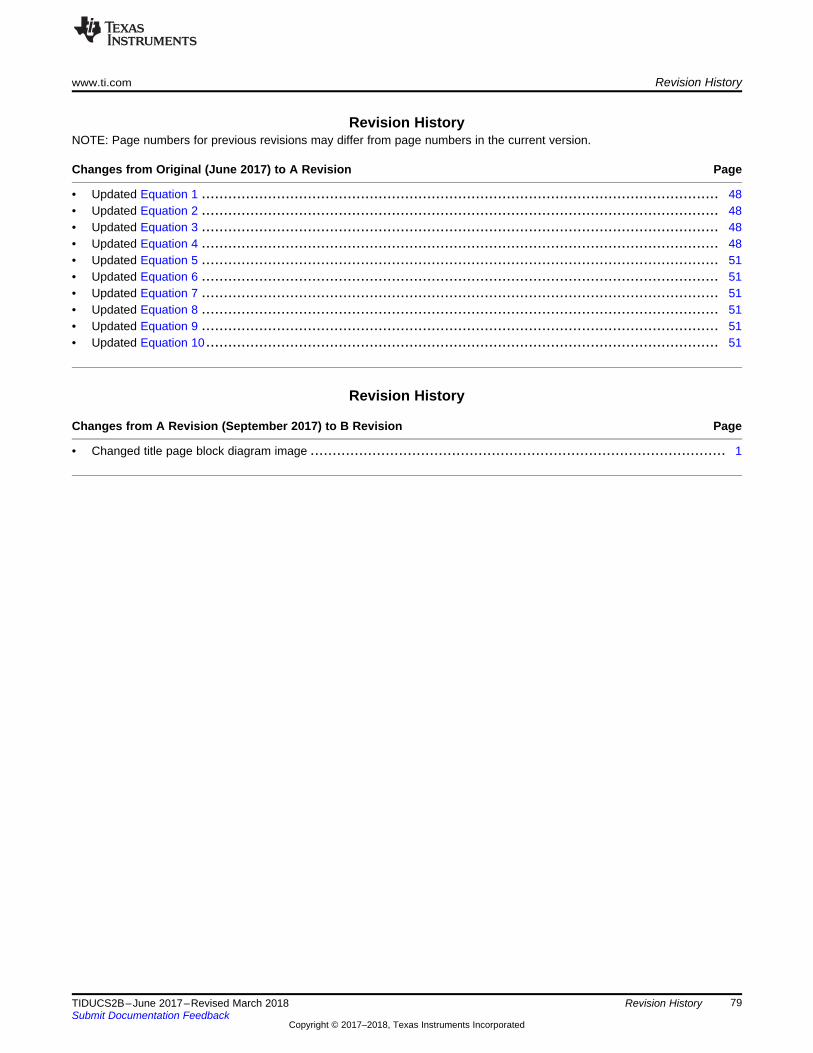
www.ti.com Revision History
79TIDUCS2B–June 2017–Revised March 2018Submit Documentation Feedback
Copyright © 2017–2018, Texas Instruments Incorporated
Revision History
Revision HistoryNOTE: Page numbers for previous revisions may differ from page numbers in the current version.
Changes from Original (June 2017) to A Revision ......................................................................................................... Page
• Updated Equation 1 ..................................................................................................................... 48• Updated Equation 2 ..................................................................................................................... 48• Updated Equation 3 ..................................................................................................................... 48• Updated Equation 4 ..................................................................................................................... 48• Updated Equation 5 ..................................................................................................................... 51• Updated Equation 6 ..................................................................................................................... 51• Updated Equation 7 ..................................................................................................................... 51• Updated Equation 8 ..................................................................................................................... 51• Updated Equation 9 ..................................................................................................................... 51• Updated Equation 10.................................................................................................................... 51
Revision History
Changes from A Revision (September 2017) to B Revision .......................................................................................... Page
• Changed title page block diagram image .............................................................................................. 1

IMPORTANT NOTICE FOR TI DESIGN INFORMATION AND RESOURCES
Texas Instruments Incorporated (‘TI”) technical, application or other design advice, services or information, including, but not limited to,reference designs and materials relating to evaluation modules, (collectively, “TI Resources”) are intended to assist designers who aredeveloping applications that incorporate TI products; by downloading, accessing or using any particular TI Resource in any way, you(individually or, if you are acting on behalf of a company, your company) agree to use it solely for this purpose and subject to the terms ofthis Notice.TI’s provision of TI Resources does not expand or otherwise alter TI’s applicable published warranties or warranty disclaimers for TIproducts, and no additional obligations or liabilities arise from TI providing such TI Resources. TI reserves the right to make corrections,enhancements, improvements and other changes to its TI Resources.You understand and agree that you remain responsible for using your independent analysis, evaluation and judgment in designing yourapplications and that you have full and exclusive responsibility to assure the safety of your applications and compliance of your applications(and of all TI products used in or for your applications) with all applicable regulations, laws and other applicable requirements. Yourepresent that, with respect to your applications, you have all the necessary expertise to create and implement safeguards that (1)anticipate dangerous consequences of failures, (2) monitor failures and their consequences, and (3) lessen the likelihood of failures thatmight cause harm and take appropriate actions. You agree that prior to using or distributing any applications that include TI products, youwill thoroughly test such applications and the functionality of such TI products as used in such applications. TI has not conducted anytesting other than that specifically described in the published documentation for a particular TI Resource.You are authorized to use, copy and modify any individual TI Resource only in connection with the development of applications that includethe TI product(s) identified in such TI Resource. NO OTHER LICENSE, EXPRESS OR IMPLIED, BY ESTOPPEL OR OTHERWISE TOANY OTHER TI INTELLECTUAL PROPERTY RIGHT, AND NO LICENSE TO ANY TECHNOLOGY OR INTELLECTUAL PROPERTYRIGHT OF TI OR ANY THIRD PARTY IS GRANTED HEREIN, including but not limited to any patent right, copyright, mask work right, orother intellectual property right relating to any combination, machine, or process in which TI products or services are used. Informationregarding or referencing third-party products or services does not constitute a license to use such products or services, or a warranty orendorsement thereof. Use of TI Resources may require a license from a third party under the patents or other intellectual property of thethird party, or a license from TI under the patents or other intellectual property of TI.TI RESOURCES ARE PROVIDED “AS IS” AND WITH ALL FAULTS. TI DISCLAIMS ALL OTHER WARRANTIES ORREPRESENTATIONS, EXPRESS OR IMPLIED, REGARDING TI RESOURCES OR USE THEREOF, INCLUDING BUT NOT LIMITED TOACCURACY OR COMPLETENESS, TITLE, ANY EPIDEMIC FAILURE WARRANTY AND ANY IMPLIED WARRANTIES OFMERCHANTABILITY, FITNESS FOR A PARTICULAR PURPOSE, AND NON-INFRINGEMENT OF ANY THIRD PARTY INTELLECTUALPROPERTY RIGHTS.TI SHALL NOT BE LIABLE FOR AND SHALL NOT DEFEND OR INDEMNIFY YOU AGAINST ANY CLAIM, INCLUDING BUT NOTLIMITED TO ANY INFRINGEMENT CLAIM THAT RELATES TO OR IS BASED ON ANY COMBINATION OF PRODUCTS EVEN IFDESCRIBED IN TI RESOURCES OR OTHERWISE. IN NO EVENT SHALL TI BE LIABLE FOR ANY ACTUAL, DIRECT, SPECIAL,COLLATERAL, INDIRECT, PUNITIVE, INCIDENTAL, CONSEQUENTIAL OR EXEMPLARY DAMAGES IN CONNECTION WITH ORARISING OUT OF TI RESOURCES OR USE THEREOF, AND REGARDLESS OF WHETHER TI HAS BEEN ADVISED OF THEPOSSIBILITY OF SUCH DAMAGES.You agree to fully indemnify TI and its representatives against any damages, costs, losses, and/or liabilities arising out of your non-compliance with the terms and provisions of this Notice.This Notice applies to TI Resources. Additional terms apply to the use and purchase of certain types of materials, TI products and services.These include; without limitation, TI’s standard terms for semiconductor products http://www.ti.com/sc/docs/stdterms.htm), evaluationmodules, and samples (http://www.ti.com/sc/docs/sampterms.htm).
Mailing Address: Texas Instruments, Post Office Box 655303, Dallas, Texas 75265Copyright © 2018, Texas Instruments Incorporated


