Embed Size (px)
Citation preview
Article
2 kW Dual-Output Isolated DC/DC Converter Basedon Current Doubler and Step-Down Chopper
Yoshinori Matsushita 1,2,* , Toshihiko Noguchi 1, Noritaka Taguchi 2 and Makoto Ishii 3
1 Graduate School of Science and Technology, Shizuoka University, Hamamatsu 432-8561, Japan;[email protected]
2 Yazaki Research and Technology Center, YAZAKI Corporation, Susono, Shizuoka 410-1194, Japan;[email protected]
3 In-Vehicle Systems R & D Center, YAZAKI Corporation, Susono, Shizuoka 410-1194, Japan;[email protected]
* Correspondence: [email protected]
Received: 5 November 2020; Accepted: 11 December 2020; Published: 14 December 2020
Abstract: In the context of the auxiliary power for motor-driven vehicles having two systems,we propose a new topology for a dual-output isolated DC/DC converter, which offers advantagesin terms of efficiency and size. The proposed circuit consists of an H-bridge inverter, a transformer,and an integrated circuit of a current doubler and step-down chopper. Considering the high power andhigh frequency, our objective was to evaluate and identify the issues of an actual device with a poweroutput of 2 kW and switching frequency of 400 kHz. The circuit feasibility was examined throughmeasurements of the prototype, and both the voltage target response and load disturbance responsecharacteristics were confirmed to operate as designed. The maximum and minimum efficienciesof this circuit were 81.3 and 61.5%, respectively, demonstrating that the load loss of the step-downchopper had a significant impact on the efficiency. The loss analysis revealed that the loss at theintegrated circuit on the secondary side accounted for more than 50% of the total loss. Moreover,issues such as the behavior at power-on, efficiency, and size were identified and evaluated, therebyachieving the objectives of the study.
Keywords: dual output; DC/DC converter; auxiliary power source; current doubler; step-down chopper
1. Introduction
Approximately one quarter of the global CO2 emissions, which are the cause of global warming,originate from the transportation sector [1]. To reduce such emissions, the automotive industry hasintroduced motor-driven vehicles such as electric vehicles (EVs), plug-in hybrid vehicles (PHVs),and fuel cell vehicles (FCVs) into the market, the sales of which continue to increase [2]. In September2020, the state of California announced a plan to ban the sale of new gasoline-driven vehicles in2035. Accordingly, the sale of motor-driven vehicles is expected to accelerate in the future. IsolatedDC/DC converters are used as auxiliary power for these motor-driven vehicles, with the power supplyfor the motor drive as the input [3,4]. The capacity and power consumption of auxiliary power isexpected to increase in the future in response to the electrification of traditionally mechanical functions,such as steering and reclining mechanisms, as well as the increase in comfort-enhancing electricalcomponents such as seat heaters [5,6]. The increased capacity leads to an increase in the conductionloss, and changing the conventional 12 V auxiliary power to 48 V has been proposed to reduce thisloss [7,8]. However, as loads that require a 12 V power supply still exist, the mixing of the two loadsystems, namely 48 and 12 V, continues to be necessary. At present, several methods are availableto realize the two systems’ auxiliary power; for example, installing two isolated DC/DC converters
World Electric Vehicle Journal 2020, 11, 78; doi:10.3390/wevj11040078 www.mdpi.com/journal/wevj
World Electric Vehicle Journal 2020, 11, 78 2 of 19
with the power supply input for the motor drive or inserting a non-isolated bidirectional DC/DCconverter for 48 and 12 V in a 48 V system [9]. However, these methods exhibit problems such as anincreased size owing to the installation of two units and reduced efficiency as a result of the two powerconversions. To overcome these issues, we propose a novel dual-output isolated DC/DC converter,which includes an integrated circuit of a current doubler and step-down chopper on the secondary sideand outputs both 48 V and 12 V [10]. Since the secondary side of the proposed circuit is an integratedcircuit and there is no need to convert voltage twice to generate 12 V, the proposed circuit is expected tohave a smaller size and higher efficiency although the control method becomes more complex. As ourprevious studies were based on simulations or a downsized prototype, no actual device testing has yetbeen performed with power for automotive applications.
Meanwhile, a demand exists for the downsizing of power converters, and one of the methods toachieve this goal is increasing the frequency. In this manner, the passive components in circuits, such asthe transformer, inductance, and capacitance, can be downsized. Therefore, substantial research hasbeen conducted on high-frequency drive power converters using switching devices made of GaN,which enable faster switching than Si devices [11–14]. However, as the frequency increases, the loss atthe downsized passive components and switching loss of the switching device also increase, leading toa larger cooling mechanism. Therefore, a specific frequency exists to realize the minimum device size.This frequency is dependent on the input/output power conditions, but it is expected to increase withthe improvement in the structures and materials of the passive components [15–17].
Within this context, we conducted a study on a novel dual-output isolated DC/DC converterwith an integrated circuit of a current doubler and step-down chopper on the secondary side,which was previously only evaluated for downsizing. We constructed an actual device with amaximum output power of 2 kW for automotive applications, examined its validity, and identified itsissues. In consideration of the trend of higher frequency as explained above, a switching frequency isset to 400 kHz, which is about two times higher than switching frequencies of existing studies on athree-port-isolated DC/DC converter [18–20].
2. Circuit Configuration and Operation Principle
2.1. Circuit Configuration
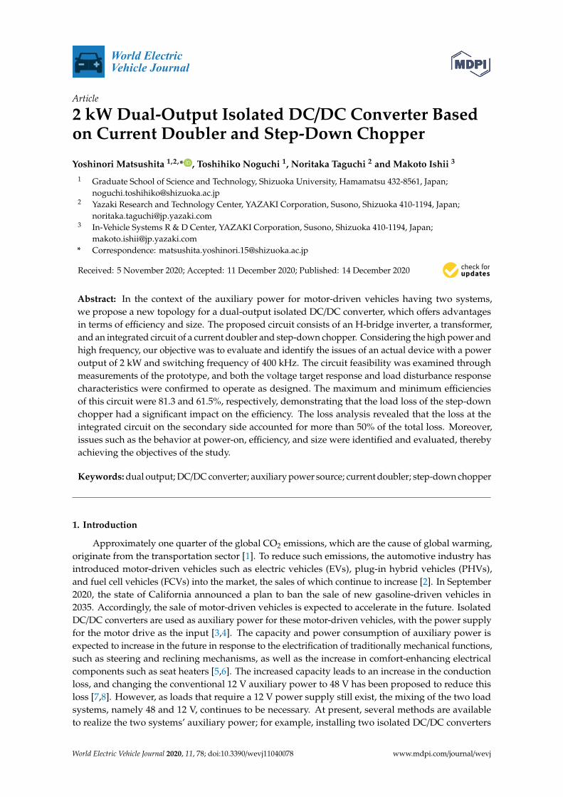
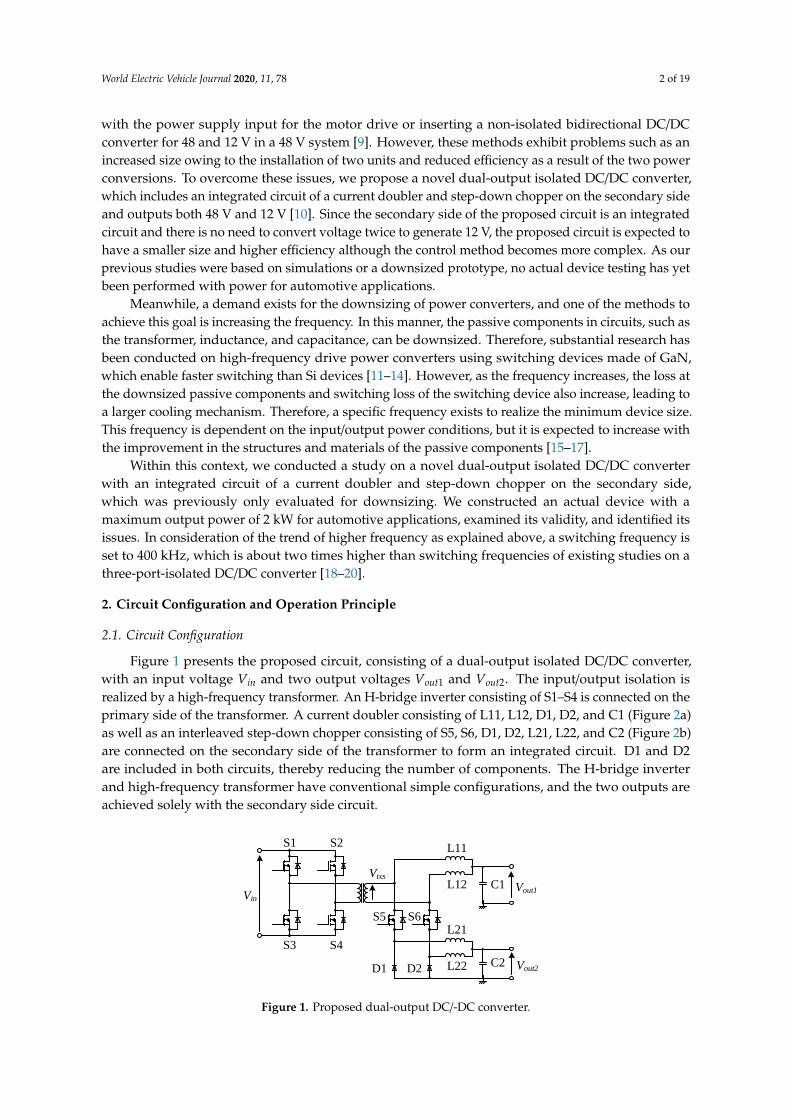
Figure 1 presents the proposed circuit, consisting of a dual-output isolated DC/DC converter,with an input voltage Vin and two output voltages Vout1 and Vout2. The input/output isolation isrealized by a high-frequency transformer. An H-bridge inverter consisting of S1–S4 is connected on theprimary side of the transformer. A current doubler consisting of L11, L12, D1, D2, and C1 (Figure 2a)as well as an interleaved step-down chopper consisting of S5, S6, D1, D2, L21, L22, and C2 (Figure 2b)are connected on the secondary side of the transformer to form an integrated circuit. D1 and D2are included in both circuits, thereby reducing the number of components. The H-bridge inverterand high-frequency transformer have conventional simple configurations, and the two outputs areachieved solely with the secondary side circuit.
World Electric Vehicle Journal 2020, 11, x 2 of 20
available to realize the two systems’ auxiliary power; for example, installing two isolated DC/DC
converters with the power supply input for the motor drive or inserting a non-isolated bidirectional
DC/DC converter for 48 and 12 V in a 48 V system [9]. However, these methods exhibit problems
such as an increased size owing to the installation of two units and reduced efficiency as a result of
the two power conversions. To overcome these issues, we propose a novel dual-output isolated
DC/DC converter, which includes an integrated circuit of a current doubler and step-down chopper
on the secondary side and outputs both 48 V and 12 V [10]. Since the secondary side of the proposed
circuit is an integrated circuit and there is no need to convert voltage twice to generate 12 V, the
proposed circuit is expected to have a smaller size and higher efficiency although the control method
becomes more complex. As our previous studies were based on simulations or a downsized
prototype, no actual device testing has yet been performed with power for automotive applications.
Meanwhile, a demand exists for the downsizing of power converters, and one of the methods to
achieve this goal is increasing the frequency. In this manner, the passive components in circuits, such
as the transformer, inductance, and capacitance, can be downsized. Therefore, substantial research
has been conducted on high-frequency drive power converters using switching devices made of GaN,
which enable faster switching than Si devices [11–14]. However, as the frequency increases, the loss
at the downsized passive components and switching loss of the switching device also increase,
leading to a larger cooling mechanism. Therefore, a specific frequency exists to realize the minimum
device size. This frequency is dependent on the input/output power conditions, but it is expected to
increase with the improvement in the structures and materials of the passive components [15–17].
Within this context, we conducted a study on a novel dual-output isolated DC/DC converter
with an integrated circuit of a current doubler and step-down chopper on the secondary side, which
was previously only evaluated for downsizing. We constructed an actual device with a maximum
output power of 2 kW for automotive applications, examined its validity, and identified its issues. In
consideration of the trend of higher frequency as explained above, a switching frequency is set to 400
kHz, which is about two times higher than switching frequencies of existing studies on a three-port-
isolated DC/DC converter [18–20].
2. Circuit Configuration and Operation Principle
2.1. Circuit Configuration
Figure 1 presents the proposed circuit, consisting of a dual-output isolated DC/DC converter,
with an input voltage Vin and two output voltages Vout1 and Vout2. The input/output isolation is realized
by a high-frequency transformer. An H-bridge inverter consisting of S1–S4 is connected on the
primary side of the transformer. A current doubler consisting of L11, L12, D1, D2, and C1 (Figure 2a)
as well as an interleaved step-down chopper consisting of S5, S6, D1, D2, L21, L22, and C2 (Figure
2b) are connected on the secondary side of the transformer to form an integrated circuit. D1 and D2
are included in both circuits, thereby reducing the number of components. The H-bridge inverter and
high-frequency transformer have conventional simple configurations, and the two outputs are
achieved solely with the secondary side circuit.
L11
L12
L21
L22
S1 S2
S3 S4
S5 S6
D1 D2
C1
C2 Vout2
Vout1Vin
Vtxs
Figure 1. Proposed dual-output DC/-DC converter. Figure 1. Proposed dual-output DC/-DC converter.
World Electric Vehicle Journal 2020, 11, 78 3 of 19World Electric Vehicle Journal 2020, 11, x 3 of 20
L11
L12
D2
C1
Vout1
D1
(a)
L21
L22
S6
D2 C2
Vout2
S5
D1
(b)
Figure 2. Decomposed configuration of secondary circuit: (a) current doubler; (b) step-down chopper.
The current paths L11 and L12 are for the current doubler output, and the current paths L21 and
L22 are for the step-down chopper output. As a result, the conduction loss is reduced by half
compared to a single-load current path. Because the phases of these currents are interleaved with a
shift of 180°, the ripple frequencies at C1 and C2 become twice the inverter frequency, which reduces
the capacity and thereby the volume of C1 and C2 by half. To maintain the interleaving symmetry,
the inductance values of L11 and L12 and of L21 and L22 should be set to the same values.
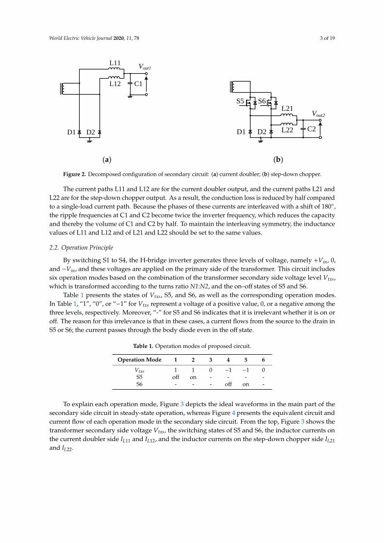
2.2. Operation Principle
By switching S1 to S4, the H-bridge inverter generates three levels of voltage, namely +Vin, 0, and
−Vin, and these voltages are applied on the primary side of the transformer. This circuit includes six
operation modes based on the combination of the transformer secondary side voltage level Vtxs, which
is transformed according to the turns ratio N1:N2, and the on–off states of S5 and S6.
Table 1 presents the states of Vtxs, S5, and S6, as well as the corresponding operation modes. In
Table 1, “1”, “0”, or “−1” for Vtxs represent a voltage of a positive value, 0, or a negative among the
three levels, respectively. Moreover, “-” for S5 and S6 indicates that it is irrelevant whether it is on or
off. The reason for this irrelevance is that in these cases, a current flows from the source to the drain
in S5 or S6; the current passes through the body diode even in the off state.
Table 1. Operation modes of proposed circuit.
Operation Mode 1 2 3 4 5 6
Vtxs 1 1 0 −1 −1 0
S5 off on - - - -
S6 - - - off on -
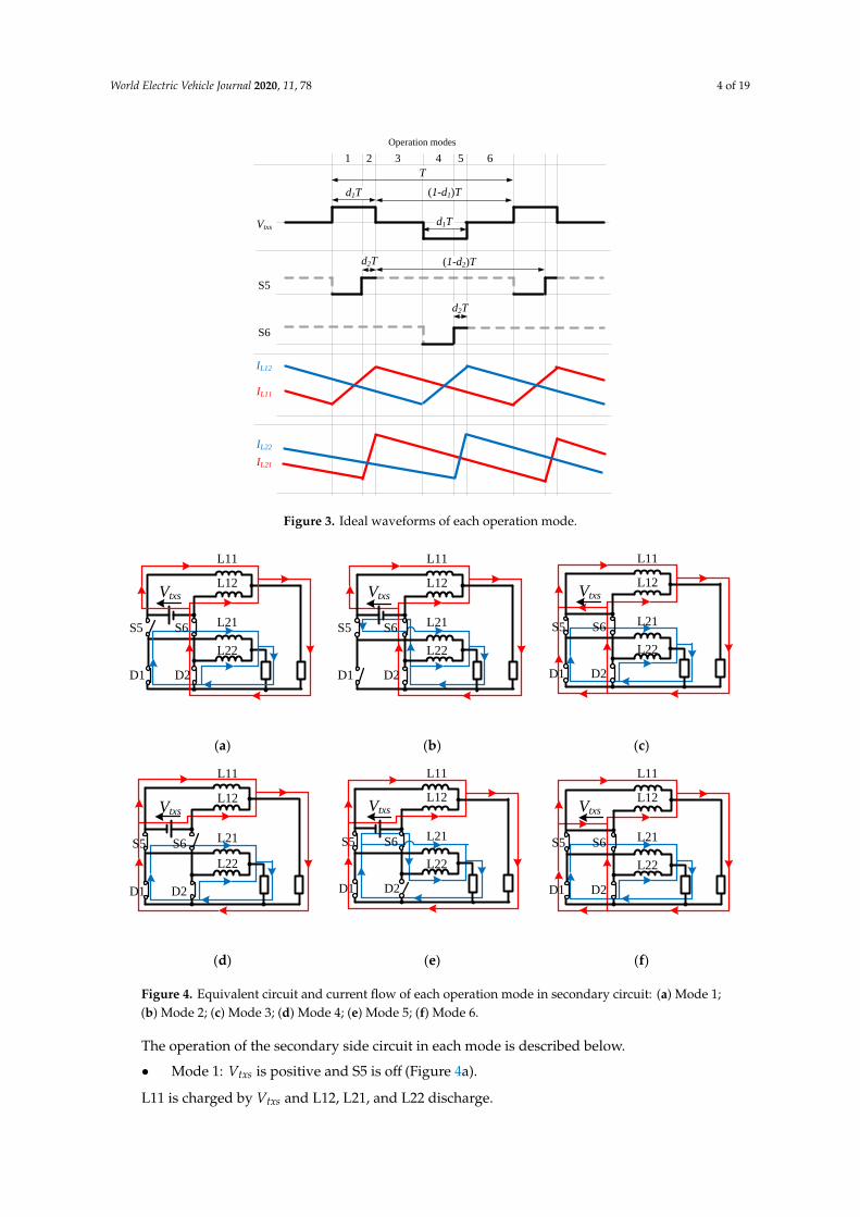
To explain each operation mode, Figure 3 depicts the ideal waveforms in the main part of the
secondary side circuit in steady-state operation, whereas Figure 4 presents the equivalent circuit and
current flow of each operation mode in the secondary side circuit. From the top, Figure 3 shows the
transformer secondary side voltage Vtxs, the switching states of S5 and S6, the inductor currents on
the current doubler side IL11 and IL12, and the inductor currents on the step-down chopper side IL21 and
IL22.
Figure 2. Decomposed configuration of secondary circuit: (a) current doubler; (b) step-down chopper.
The current paths L11 and L12 are for the current doubler output, and the current paths L21 andL22 are for the step-down chopper output. As a result, the conduction loss is reduced by half comparedto a single-load current path. Because the phases of these currents are interleaved with a shift of 180,the ripple frequencies at C1 and C2 become twice the inverter frequency, which reduces the capacityand thereby the volume of C1 and C2 by half. To maintain the interleaving symmetry, the inductancevalues of L11 and L12 and of L21 and L22 should be set to the same values.
2.2. Operation Principle
By switching S1 to S4, the H-bridge inverter generates three levels of voltage, namely +Vin, 0,and −Vin, and these voltages are applied on the primary side of the transformer. This circuit includessix operation modes based on the combination of the transformer secondary side voltage level Vtxs,which is transformed according to the turns ratio N1:N2, and the on–off states of S5 and S6.
Table 1 presents the states of Vtxs, S5, and S6, as well as the corresponding operation modes.In Table 1, “1”, “0”, or “−1” for Vtxs represent a voltage of a positive value, 0, or a negative among thethree levels, respectively. Moreover, “-” for S5 and S6 indicates that it is irrelevant whether it is on oroff. The reason for this irrelevance is that in these cases, a current flows from the source to the drain inS5 or S6; the current passes through the body diode even in the off state.
Table 1. Operation modes of proposed circuit.
Operation Mode 1 2 3 4 5 6
Vtxs 1 1 0 −1 −1 0S5 off on - - - -S6 - - - off on -
To explain each operation mode, Figure 3 depicts the ideal waveforms in the main part of thesecondary side circuit in steady-state operation, whereas Figure 4 presents the equivalent circuit andcurrent flow of each operation mode in the secondary side circuit. From the top, Figure 3 shows thetransformer secondary side voltage Vtxs, the switching states of S5 and S6, the inductor currents onthe current doubler side IL11 and IL12, and the inductor currents on the step-down chopper side IL21
and IL22.
World Electric Vehicle Journal 2020, 11, 78 4 of 19
World Electric Vehicle Journal 2020, 11, x 4 of 20
S5
Vtxs
IL21
IL22
S6
1 2 3 4 6
Operation modes
5
d2T
d2T
T
d1T
d1T (1-d1)T
(1-d2)T
IL11
IL12
Figure 3. Ideal waveforms of each operation mode.
L11
L12
L21
L22
Vtxs
S5
D1
S6
D2
(a)
L11
L12
L21
L22
Vtxs
S5
D1
S6
D2
(b)
L11
L12
L21
L22
Vtxs
S5
D1
S6
D2
(c)
L11
L12
L21
L22
Vtxs
S5
D1
S6
D2
(d)
L11
L12
L21
L22
Vtxs
S5
D1
S6
D2
(e)
L11
L12
L21
L22
Vtxs
S5
D1
S6
D2
(f)
Figure 4. Equivalent circuit and current flow of each operation mode in secondary circuit: (a) Mode
1; (b) Mode 2; (c) Mode 3; (d) Mode 4; (e) Mode 5; (f) Mode 6.
The operation of the secondary side circuit in each mode is described below.
Mode 1: Vtxs is positive and S5 is off (Figure 4a).
L11 is charged by Vtxs and L12, L21, and L22 discharge.
Mode 2: Vtxs is positive and S5 is on (Figure 4b).
Figure 3. Ideal waveforms of each operation mode.
World Electric Vehicle Journal 2020, 11, x 4 of 20
S5
Vtxs
IL21
IL22
S6
1 2 3 4 6
Operation modes
5
d2T
d2T
T
d1T
d1T (1-d1)T
(1-d2)T
IL11
IL12
Figure 3. Ideal waveforms of each operation mode.
L11
L12
L21
L22
Vtxs
S5
D1
S6
D2
L11
L12
L21
L22
Vtxs
S5
D1
S6
D2
L11
L12
L21
L22
Vtxs
S5
D1
S6
D2
(a) (b) (c)
L11
L12
L21
L22
Vtxs
S5
D1
S6
D2
L11
L12
L21
L22
Vtxs
S5
D1
S6
D2
L11
L12
L21
L22
Vtxs
S5
D1
S6
D2
(d) (e) (f)
Figure 4. Equivalent circuit and current flow of each operation mode in secondary circuit: (a) Mode
1; (b) Mode 2; (c) Mode 3; (d) Mode 4; (e) Mode 5; (f) Mode 6.
The operation of the secondary side circuit in each mode is described below.
Mode 1: Vtxs is positive and S5 is off (Figure 4a).
L11 is charged by Vtxs and L12, L21, and L22 discharge.
Mode 2: Vtxs is positive and S5 is on (Figure 4b).
As S5 is turned on, both L11 and L21 are charged by Vtxs, whereas L12 and L22 still discharge.
Mode 3: Vtxs is 0 (Figure 4c).
Figure 4. Equivalent circuit and current flow of each operation mode in secondary circuit: (a) Mode 1;(b) Mode 2; (c) Mode 3; (d) Mode 4; (e) Mode 5; (f) Mode 6.
The operation of the secondary side circuit in each mode is described below.
• Mode 1: Vtxs is positive and S5 is off (Figure 4a).
L11 is charged by Vtxs and L12, L21, and L22 discharge.

World Electric Vehicle Journal 2020, 11, 78 5 of 19
• Mode 2: Vtxs is positive and S5 is on (Figure 4b).
As S5 is turned on, both L11 and L21 are charged by Vtxs, whereas L12 and L22 still discharge.
• Mode 3: Vtxs is 0 (Figure 4c).
When Vtxs is 0, there is no power, and therefore, L11, L12, L21, and L22 all discharge.
• Mode 4: Vtxs is negative and S6 is off (Figure 4d).
L12 is charged by Vtxs and L11, L21, and L22 discharge.
• Mode 5: Vtxs is negative and S6 is on (Figure 4e).
As S6 is turned on, L12 as well as L22 are charged. L11 and L21 still discharge.
• Mode 6: Vtxs is 0 (Figure 4f).
As in Mode 3, as Vtxs is 0, L11, L12, L21, and L22 discharge.
Table 2 displays the output voltages of the proposed circuit in the steady-state operation Vout1 andVout2; the output currents Iout1 and Iout2; the output average inductor currents IL11, IL12, IL21, and IL22;the inductor current ripple factors γL11, γL12, γL21, and γL22; and the capacitor ripple currents ∆ic1 and∆ic2. In this case, d1 and d2 in the equations are duty ratios for the period in which Vtxs is positive ornegative and for the period of Mode 2 or Mode 5, respectively, as illustrated in Figure 3. L1 and L2 are theinductance values of L11 or L12 and L21 or L22, respectively. R1 and R2 are the load resistance values ofthe current doubler and step-down chopper outputs, respectively. Moreover, T is the time of one cycle.
Table 2. Theoretical formulas of proposed circuit.
Symbol Value Symbol Value
Vout1d1N2Vin
N1Vout2
d2N2VinN1
Iout1d1N2Vin
N1R1Iout2
d2N2VinN1R2
IL11IL12
d1N2Vin2N1R1
IL21IL22
d2N2Vin2N1R2
γL11γL12
2R1(1− d1)TL1
γL21γL22
2R2(1− d2)TL2
∆ic1R1(1− d1)TIout1
L1∆ic2
R2(1− d2)TIout2
L2
As indicated in Table 2, when Vin is constant, Vout1 and Vout2 are only dependent on the duty ratiocorresponding to each of these. That is, the switching of S1 to S4 controls Vout1, and that of S5 and S6controls Vout2. This means that Vout1 and Vout2 can be controlled independently; however, this is onlypossible when the circuit operates with the six operation modes described above. This means that thefollowing condition must be satisfied:
d1 > d2. (1)
If Equation (1) is not true (d1 5 d2), S5 and S6 are always on, while the transformer is transmittingpower from the primary side to the secondary side (when Vtxs is positive or negative). Consequently,there will be no means of controlling Vout2 and the dual-output converter cannot perform its function.
3. Actual Device Testing
3.1. Main Circuit Configuration
Table 3 summarizes the specifications of the experimental circuit that was constructed to operatethe proposed circuit at 400 kHz and 2 kW, the configuration and appearance of which are presented
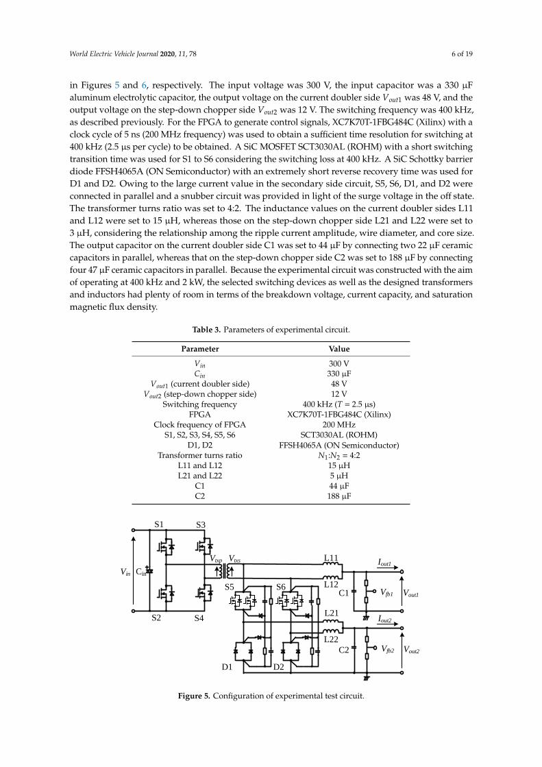
World Electric Vehicle Journal 2020, 11, 78 6 of 19
in Figures 5 and 6, respectively. The input voltage was 300 V, the input capacitor was a 330 µFaluminum electrolytic capacitor, the output voltage on the current doubler side Vout1 was 48 V, and theoutput voltage on the step-down chopper side Vout2 was 12 V. The switching frequency was 400 kHz,as described previously. For the FPGA to generate control signals, XC7K70T-1FBG484C (Xilinx) with aclock cycle of 5 ns (200 MHz frequency) was used to obtain a sufficient time resolution for switching at400 kHz (2.5 µs per cycle) to be obtained. A SiC MOSFET SCT3030AL (ROHM) with a short switchingtransition time was used for S1 to S6 considering the switching loss at 400 kHz. A SiC Schottky barrierdiode FFSH4065A (ON Semiconductor) with an extremely short reverse recovery time was used forD1 and D2. Owing to the large current value in the secondary side circuit, S5, S6, D1, and D2 wereconnected in parallel and a snubber circuit was provided in light of the surge voltage in the off state.The transformer turns ratio was set to 4:2. The inductance values on the current doubler sides L11and L12 were set to 15 µH, whereas those on the step-down chopper side L21 and L22 were set to3 µH, considering the relationship among the ripple current amplitude, wire diameter, and core size.The output capacitor on the current doubler side C1 was set to 44 µF by connecting two 22 µF ceramiccapacitors in parallel, whereas that on the step-down chopper side C2 was set to 188 µF by connectingfour 47 µF ceramic capacitors in parallel. Because the experimental circuit was constructed with the aimof operating at 400 kHz and 2 kW, the selected switching devices as well as the designed transformersand inductors had plenty of room in terms of the breakdown voltage, current capacity, and saturationmagnetic flux density.
Table 3. Parameters of experimental circuit.
Parameter Value
Vin 300 VCin 330 µF
Vout1 (current doubler side) 48 VVout2 (step-down chopper side) 12 V
Switching frequency 400 kHz (T = 2.5 µs)FPGA XC7K70T-1FBG484C (Xilinx)
Clock frequency of FPGA 200 MHzS1, S2, S3, S4, S5, S6 SCT3030AL (ROHM)
D1, D2 FFSH4065A (ON Semiconductor)Transformer turns ratio N1:N2 = 4:2
L11 and L12 15 µHL21 and L22 5 µH
C1 44 µFC2 188 µF
World Electric Vehicle Journal 2020, 11, x 6 of 20
switching at 400 kHz (2.5 μs per cycle) to be obtained. A SiC MOSFET SCT3030AL (ROHM) with a
short switching transition time was used for S1 to S6 considering the switching loss at 400 kHz. A SiC
Schottky barrier diode FFSH4065A (ON Semiconductor) with an extremely short reverse recovery
time was used for D1 and D2. Owing to the large current value in the secondary side circuit, S5, S6,
D1, and D2 were connected in parallel and a snubber circuit was provided in light of the surge voltage
in the off state. The transformer turns ratio was set to 4:2. The inductance values on the current
doubler sides L11 and L12 were set to 15 μH, whereas those on the step-down chopper side L21 and
L22 were set to 3 μH, considering the relationship among the ripple current amplitude, wire diameter,
and core size. The output capacitor on the current doubler side C1 was set to 44 μF by connecting
two 22 μF ceramic capacitors in parallel, whereas that on the step-down chopper side C2 was set to
188 μF by connecting four 47 μF ceramic capacitors in parallel. Because the experimental circuit was
constructed with the aim of operating at 400 kHz and 2 kW, the selected switching devices as well as
the designed transformers and inductors had plenty of room in terms of the breakdown voltage,
current capacity, and saturation magnetic flux density.
Table 3. Parameters of experimental circuit.
Parameter Value
Vin 300 V
Cin 330 μF
Vout1 (current doubler side) 48 V
Vout2 (step-down chopper side) 12 V
Switching frequency 400 kHz (T = 2.5 μs)
FPGA XC7K70T-1FBG484C (Xilinx)
Clock frequency of FPGA 200 MHz
S1, S2, S3, S4, S5, S6 SCT3030AL (ROHM)
D1, D2 FFSH4065A (ON Semiconductor)
Transformer turns ratio N1:N2 = 4:2
L11 and L12 15 μH
L21 and L22 5 μH
C1 44 μF
C2 188 μF
S1
S2
S3
S4
S5 S6Vout1
Vout2
Vin
Vfb1
Vfb2
C1
C2
L11
L12
L21
L22
Cin
D1 D2
VtxsVtxp Iout1
Iout2
Figure 5. Configuration of experimental test circuit. Figure 5. Configuration of experimental test circuit.
World Electric Vehicle Journal 2020, 11, 78 7 of 19
World Electric Vehicle Journal 2020, 11, x 7 of 20
(a)
(b)
Figure 6. Experimental circuit setup: (a) main circuit with control circuit; (b) main circuit without
control circuit.
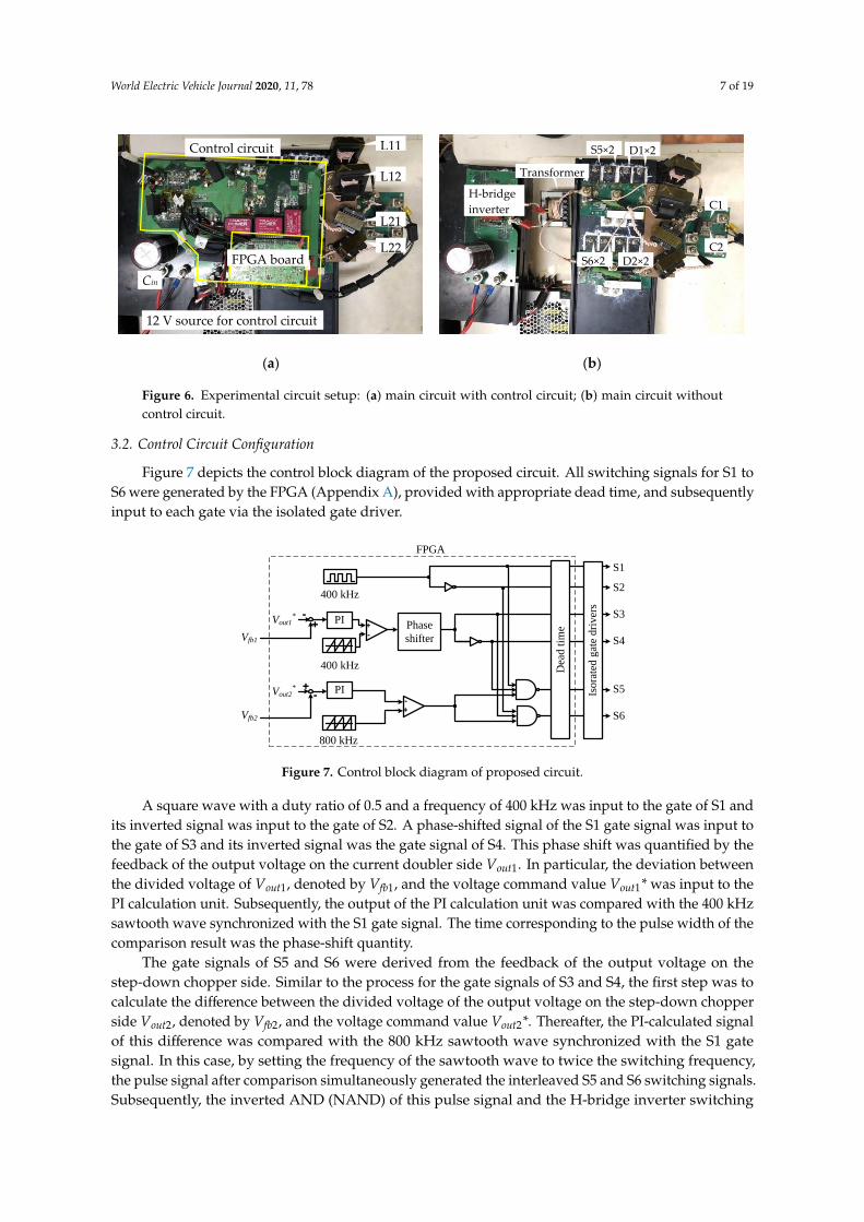
3.2. Control Circuit Configuration
Figure 7 depicts the control block diagram of the proposed circuit. All switching signals for S1
to S6 were generated by the FPGA, provided with appropriate dead time, and subsequently input to
each gate via the isolated gate driver.
+
-
+
-
+-
+-
Vout1*
PIPhase
shifter
Vout2* PI S5
S6
S1
S2
S3
S4
400 kHz
Vfb1
Vfb2
400 kHz
800 kHz
Dea
d t
ime
FPGA
Iso
rate
d g
ate
dri
ver
s
Figure 7. Control block diagram of proposed circuit.
A square wave with a duty ratio of 0.5 and a frequency of 400 kHz was input to the gate of S1
and its inverted signal was input to the gate of S2. A phase-shifted signal of the S1 gate signal was
input to the gate of S3 and its inverted signal was the gate signal of S4. This phase shift was quantified
by the feedback of the output voltage on the current doubler side Vout1. In particular, the deviation
between the divided voltage of Vout1, denoted by Vfb1, and the voltage command value Vout1* was input
to the PI calculation unit. Subsequently, the output of the PI calculation unit was compared with the
400 kHz sawtooth wave synchronized with the S1 gate signal. The time corresponding to the pulse
width of the comparison result was the phase-shift quantity.
The gate signals of S5 and S6 were derived from the feedback of the output voltage on the step-
down chopper side. Similar to the process for the gate signals of S3 and S4, the first step was to
calculate the difference between the divided voltage of the output voltage on the step-down chopper
side Vout2, denoted by Vfb2, and the voltage command value Vout2*. Thereafter, the PI-calculated signal
of this difference was compared with the 800 kHz sawtooth wave synchronized with the S1 gate
signal. In this case, by setting the frequency of the sawtooth wave to twice the switching frequency,
the pulse signal after comparison simultaneously generated the interleaved S5 and S6 switching
signals. Subsequently, the inverted AND (NAND) of this pulse signal and the H-bridge inverter
switching signal was created to enable the assigned switching of S5 when Vtxs was positive and that
of S6 when Vtxs was negative, as demonstrated in Table 1 and Figure 3. For the modes in Table 1, in
12 V source for control circuit
Cin
L11
L12
L21
L22 FPGA board
Control circuit
H-bridge
inverter C1
C2
Transformer
S5×2 D1×2
S6×2 D2×2
Figure 6. Experimental circuit setup: (a) main circuit with control circuit; (b) main circuit withoutcontrol circuit.
3.2. Control Circuit Configuration
Figure 7 depicts the control block diagram of the proposed circuit. All switching signals for S1 toS6 were generated by the FPGA (Appendix A), provided with appropriate dead time, and subsequentlyinput to each gate via the isolated gate driver.
World Electric Vehicle Journal 2020, 11, x 7 of 20
(a)
(b)
Figure 6. Experimental circuit setup: (a) main circuit with control circuit; (b) main circuit without
control circuit.
3.2. Control Circuit Configuration
Figure 7 depicts the control block diagram of the proposed circuit. All switching signals for S1
to S6 were generated by the FPGA, provided with appropriate dead time, and subsequently input to
each gate via the isolated gate driver.
+
-
+
-
+-
+-
Vout1*
PIPhase
shifter
Vout2* PI S5
S6
S1
S2
S3
S4
400 kHz
Vfb1
Vfb2
400 kHz
800 kHz
Dea
d t
ime
FPGA
Iso
rate
d g
ate
dri
ver
s
Figure 7. Control block diagram of proposed circuit.
A square wave with a duty ratio of 0.5 and a frequency of 400 kHz was input to the gate of S1
and its inverted signal was input to the gate of S2. A phase-shifted signal of the S1 gate signal was
input to the gate of S3 and its inverted signal was the gate signal of S4. This phase shift was quantified
by the feedback of the output voltage on the current doubler side Vout1. In particular, the deviation
between the divided voltage of Vout1, denoted by Vfb1, and the voltage command value Vout1* was input
to the PI calculation unit. Subsequently, the output of the PI calculation unit was compared with the
400 kHz sawtooth wave synchronized with the S1 gate signal. The time corresponding to the pulse
width of the comparison result was the phase-shift quantity.
The gate signals of S5 and S6 were derived from the feedback of the output voltage on the step-
down chopper side. Similar to the process for the gate signals of S3 and S4, the first step was to
calculate the difference between the divided voltage of the output voltage on the step-down chopper
side Vout2, denoted by Vfb2, and the voltage command value Vout2*. Thereafter, the PI-calculated signal
of this difference was compared with the 800 kHz sawtooth wave synchronized with the S1 gate
signal. In this case, by setting the frequency of the sawtooth wave to twice the switching frequency,
the pulse signal after comparison simultaneously generated the interleaved S5 and S6 switching
signals. Subsequently, the inverted AND (NAND) of this pulse signal and the H-bridge inverter
switching signal was created to enable the assigned switching of S5 when Vtxs was positive and that
of S6 when Vtxs was negative, as demonstrated in Table 1 and Figure 3. For the modes in Table 1, in
12 V source for control circuit
Cin
L11
L12
L21
L22 FPGA board
Control circuit
H-bridge
inverter C1
C2
Transformer
S5×2 D1×2
S6×2 D2×2
Figure 7. Control block diagram of proposed circuit.
A square wave with a duty ratio of 0.5 and a frequency of 400 kHz was input to the gate of S1 andits inverted signal was input to the gate of S2. A phase-shifted signal of the S1 gate signal was input tothe gate of S3 and its inverted signal was the gate signal of S4. This phase shift was quantified by thefeedback of the output voltage on the current doubler side Vout1. In particular, the deviation betweenthe divided voltage of Vout1, denoted by Vfb1, and the voltage command value Vout1* was input to thePI calculation unit. Subsequently, the output of the PI calculation unit was compared with the 400 kHzsawtooth wave synchronized with the S1 gate signal. The time corresponding to the pulse width of thecomparison result was the phase-shift quantity.
The gate signals of S5 and S6 were derived from the feedback of the output voltage on thestep-down chopper side. Similar to the process for the gate signals of S3 and S4, the first step was tocalculate the difference between the divided voltage of the output voltage on the step-down chopperside Vout2, denoted by Vfb2, and the voltage command value Vout2*. Thereafter, the PI-calculated signalof this difference was compared with the 800 kHz sawtooth wave synchronized with the S1 gatesignal. In this case, by setting the frequency of the sawtooth wave to twice the switching frequency,the pulse signal after comparison simultaneously generated the interleaved S5 and S6 switching signals.Subsequently, the inverted AND (NAND) of this pulse signal and the H-bridge inverter switching
World Electric Vehicle Journal 2020, 11, 78 8 of 19
signal was created to enable the assigned switching of S5 when Vtxs was positive and that of S6 whenVtxs was negative, as demonstrated in Table 1 and Figure 3. For the modes in Table 1, in which theswitching states of S5 and S6 were irrelevant, S5 and S6 were turned on to prevent loss owing to acurrent flow to the body diode.
3.3. Operation Points
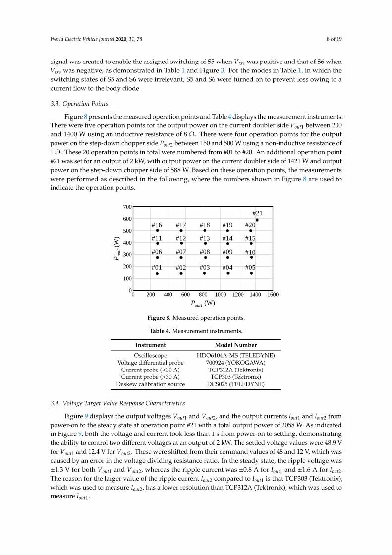
Figure 8 presents the measured operation points and Table 4 displays the measurement instruments.There were five operation points for the output power on the current doubler side Pout1 between 200and 1400 W using an inductive resistance of 8 Ω. There were four operation points for the outputpower on the step-down chopper side Pout2 between 150 and 500 W using a non-inductive resistance of1 Ω. These 20 operation points in total were numbered from #01 to #20. An additional operation point#21 was set for an output of 2 kW, with output power on the current doubler side of 1421 W and outputpower on the step-down chopper side of 588 W. Based on these operation points, the measurementswere performed as described in the following, where the numbers shown in Figure 8 are used toindicate the operation points.
World Electric Vehicle Journal 2020, 11, x 8 of 20
which the switching states of S5 and S6 were irrelevant, S5 and S6 were turned on to prevent loss
owing to a current flow to the body diode.
3.3. Operation Points
Figure 8 presents the measured operation points and Table 4 displays the measurement
instruments. There were five operation points for the output power on the current doubler side Pout1
between 200 and 1400 W using an inductive resistance of 8 Ω. There were four operation points for
the output power on the step-down chopper side Pout2 between 150 and 500 W using a non-inductive
resistance of 1 Ω. These 20 operation points in total were numbered from #01 to #20. An additional
operation point #21 was set for an output of 2 kW, with output power on the current doubler side of
1421 W and output power on the step-down chopper side of 588 W. Based on these operation points,
the measurements were performed as described in the following, where the numbers shown in Figure
8 are used to indicate the operation points.
Figure 8. Measured operation points.
Table 4. Measurement instruments.
Instrument Model Number
Oscilloscope HDO6104A-MS (TELEDYNE)
Voltage differential probe 700924 (YOKOGAWA)
Current probe (<30 A) TCP312A (Tektronix)
Current probe (>30 A) TCP303 (Tektronix)
Deskew calibration source DCS025 (TELEDYNE)
3.4. Voltage Target Value Response Characteristics
Figure 9 displays the output voltages Vout1 and Vout2, and the output currents Iout1 and Iout2 from
power-on to the steady state at operation point #21 with a total output power of 2058 W. As indicated
in Figure 9, both the voltage and current took less than 1 s from power-on to settling, demonstrating
the ability to control two different voltages at an output of 2 kW. The settled voltage values were 48.9
V for Vout1 and 12.4 V for Vout2. These were shifted from their command values of 48 and 12 V, which
was caused by an error in the voltage dividing resistance ratio. In the steady state, the ripple voltage
was ±1.3 V for both Vout1 and Vout2, whereas the ripple current was ±0.8 A for Iout1 and ±1.6 A for Iout2.
The reason for the larger value of the ripple current Iout2 compared to Iout1 is that TCP303 (Tektronix),
which was used to measure Iout2, has a lower resolution than TCP312A (Tektronix), which was used
to measure Iout1.
0 200 400 600 800 1000 1200 1400 16000
100
200
300
400
500
600
700#21
Pout2
(W
)
Pout1 (W)
#01 #02 #03 #04 #05
#06 #07 #08 #09 #10
#11 #12 #15#13 #14
#16 #17 #18 #19 #20
Figure 8. Measured operation points.
Table 4. Measurement instruments.
Instrument Model Number
Oscilloscope HDO6104A-MS (TELEDYNE)Voltage differential probe 700924 (YOKOGAWA)
Current probe (<30 A) TCP312A (Tektronix)Current probe (>30 A) TCP303 (Tektronix)
Deskew calibration source DCS025 (TELEDYNE)
3.4. Voltage Target Value Response Characteristics
Figure 9 displays the output voltages Vout1 and Vout2, and the output currents Iout1 and Iout2 frompower-on to the steady state at operation point #21 with a total output power of 2058 W. As indicatedin Figure 9, both the voltage and current took less than 1 s from power-on to settling, demonstratingthe ability to control two different voltages at an output of 2 kW. The settled voltage values were 48.9 Vfor Vout1 and 12.4 V for Vout2. These were shifted from their command values of 48 and 12 V, which wascaused by an error in the voltage dividing resistance ratio. In the steady state, the ripple voltage was±1.3 V for both Vout1 and Vout2, whereas the ripple current was ±0.8 A for Iout1 and ±1.6 A for Iout2.The reason for the larger value of the ripple current Iout2 compared to Iout1 is that TCP303 (Tektronix),which was used to measure Iout2, has a lower resolution than TCP312A (Tektronix), which was used tomeasure Iout1.
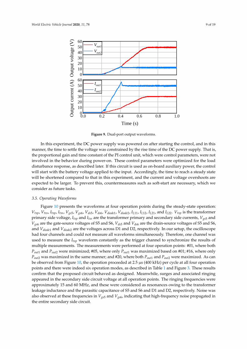
World Electric Vehicle Journal 2020, 11, 78 9 of 19World Electric Vehicle Journal 2020, 11, x 9 of 20
Figure 9. Dual-port output waveforms.
In this experiment, the DC power supply was powered on after starting the control, and in this
manner, the time to settle the voltage was constrained by the rise time of the DC power supply. That
is, the proportional gain and time constant of the PI control unit, which were control parameters,
were not involved in the behavior during power-on. These control parameters were optimized for
the load disturbance response, as described later. If this circuit is used as on-board auxiliary power,
the control will start with the battery voltage applied to the input. Accordingly, the time to reach a
steady state will be shortened compared to that in this experiment, and the current and voltage
overshoots are expected to be larger. To prevent this, countermeasures such as soft-start are necessary,
which we consider as future tasks.
3.5. Operating Waveforms
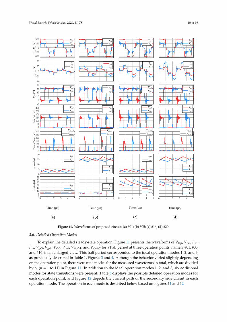
Figure 10 presents the waveforms at four operation points during the steady-state operation: Vtxp,
Vtxs, Itxp, Itxs, Vgs5, Vgs6, Vds5, Vds6, Vdiode1, Vdiode2, IL11, IL12, IL21, and IL22. Vtxp is the transformer primary side
voltage, Itxp and Itxs are the transformer primary and secondary side currents, Vgs5 and Vgs6 are the gate-
source voltages of S5 and S6, Vds5 and Vds6 are the drain-source voltages of S5 and S6, and Vdiode1 and
Vdiode2 are the voltages across D1 and D2, respectively. In our setup, the oscilloscope had four channels
and could not measure all waveforms simultaneously. Therefore, one channel was used to measure
the Itxp waveform constantly as the trigger channel to synchronize the results of multiple
measurements. The measurements were performed at four operation points: #01, where both Pout1 and
Pout2 were minimized; #05, where only Pout1 was maximized based on #01; #16, where only Pout2 was
maximized in the same manner; and #20, where both Pout1 and Pout2 were maximized. As can be
observed from Figure 10, the operation proceeded at 2.5 μs (400 kHz) per cycle at all four operation
points and there were indeed six operation modes, as described in Table 1 and Figure 3. These results
confirm that the proposed circuit behaved as designed. Meanwhile, surges and associated ringing
appeared in the secondary side circuit voltage at all operation points. The ringing frequencies were
approximately 15 and 60 MHz, and these were considered as resonances owing to the transformer
leakage inductance and the parasitic capacitance of S5 and S6 and D1 and D2, respectively. Noise was
also observed at these frequencies in Vgs5 and Vgs6, indicating that high-frequency noise propagated in
the entire secondary side circuit.
0
10
20
30
40
50
60
0.0 0.2 0.4 0.6 0.8 1.00
10
20
30
40
50
60
Vout1
Vout2
Outp
ut
volt
age
(V)
Outp
ut
curr
ent
(A)
Time (s)
Iout1
Iout2
Figure 9. Dual-port output waveforms.
In this experiment, the DC power supply was powered on after starting the control, and in thismanner, the time to settle the voltage was constrained by the rise time of the DC power supply. That is,the proportional gain and time constant of the PI control unit, which were control parameters, were notinvolved in the behavior during power-on. These control parameters were optimized for the loaddisturbance response, as described later. If this circuit is used as on-board auxiliary power, the controlwill start with the battery voltage applied to the input. Accordingly, the time to reach a steady statewill be shortened compared to that in this experiment, and the current and voltage overshoots areexpected to be larger. To prevent this, countermeasures such as soft-start are necessary, which weconsider as future tasks.
3.5. Operating Waveforms
Figure 10 presents the waveforms at four operation points during the steady-state operation:Vtxp, Vtxs, Itxp, Itxs, Vgs5, Vgs6, Vds5, Vds6, Vdiode1, Vdiode2, IL11, IL12, IL21, and IL22. Vtxp is the transformerprimary side voltage, Itxp and Itxs are the transformer primary and secondary side currents, Vgs5 andVgs6 are the gate-source voltages of S5 and S6, Vds5 and Vds6 are the drain-source voltages of S5 and S6,and Vdiode1 and Vdiode2 are the voltages across D1 and D2, respectively. In our setup, the oscilloscopehad four channels and could not measure all waveforms simultaneously. Therefore, one channel wasused to measure the Itxp waveform constantly as the trigger channel to synchronize the results ofmultiple measurements. The measurements were performed at four operation points: #01, where bothPout1 and Pout2 were minimized; #05, where only Pout1 was maximized based on #01; #16, where onlyPout2 was maximized in the same manner; and #20, where both Pout1 and Pout2 were maximized. As canbe observed from Figure 10, the operation proceeded at 2.5 µs (400 kHz) per cycle at all four operationpoints and there were indeed six operation modes, as described in Table 1 and Figure 3. These resultsconfirm that the proposed circuit behaved as designed. Meanwhile, surges and associated ringingappeared in the secondary side circuit voltage at all operation points. The ringing frequencies wereapproximately 15 and 60 MHz, and these were considered as resonances owing to the transformerleakage inductance and the parasitic capacitance of S5 and S6 and D1 and D2, respectively. Noise wasalso observed at these frequencies in Vgs5 and Vgs6, indicating that high-frequency noise propagated inthe entire secondary side circuit.
World Electric Vehicle Journal 2020, 11, 78 10 of 19
World Electric Vehicle Journal 2020, 11, x 10 of 20
Time (μs)
(a)
Time (μs)
(b)
Time (μs)
(c)
Time (μs)
(d)
Figure 10. Waveforms of proposed circuit: (a) #01; (b) #05; (c) #16; (d) #20.
3.6. Detailed Operation Modes
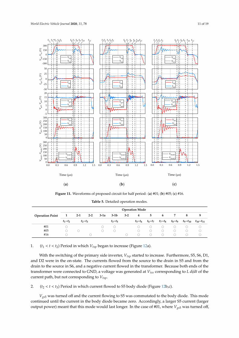
To explain the detailed steady-state operation, Figure 11 presents the waveforms of Vtxp, Vtxs, Itxp,
Itxs, Vgs5, Vgs6, Vds5, Vds6, Vdiode1, and Vdiode2 for a half period at three operation points, namely #01, #05, and
#16, in an enlarged view. This half period corresponded to the ideal operation modes 1, 2, and 3, as
previously described in Table 1, Figures 3 and 4. Although the behavior varied slightly depending
on the operation point, there were nine modes for the measured waveforms in total, which are
divided by tn (n = 1 to 11) in Figure 11. In addition to the ideal operation modes 1, 2, and 3, six
additional modes for state transitions were present. Table 5 displays the possible detailed operation
modes for each operation point, and Figure 12 depicts the current path of the secondary side circuit
in each operation mode. The operation in each mode is described below based on Figures 11 and 12.
-300
-150
0
150
300
-50
-25
0
25
50
0
5
10
15
20
0
50
100
150
200
250
300
-5
0
5
10
15
20
0 1 2 3 4 50
5
10
15
20
25
30
35
0
50
100
150
200
250
300
Vtx
p, V
txs
(V)
Vtxp
Vtxs
I txp, I tx
s (V
)
Itxp
Itxs
I L1, I L
2 (
A)
IL11
IL12
Vd
s5, V
ds6
(V
)
Vds5
Vds6
Vgs5
Vgs6
Vg
s5 (
V)
I L3, I L
4 (
A)
IL21
IL22
Vd
iod
e1, V
dio
de2
(V
)
Vdiode1
Vdiode2
-300
-150
0
150
300
-50
-25
0
25
50
0
5
10
15
20
0
50
100
150
200
250
300
-5
0
5
10
15
20
0 1 2 3 4 50
5
10
15
20
25
30
35
0
50
100
150
200
250
300
Vtx
p, V
txs
(V)
Vtxp
Vtxs
I txp, I tx
s (V
)
Itxp
Itxs
I L1, I L
2 (
A)
IL11
IL12
Vds5
, V
ds6
(V
)
Vds5
Vds6
Vgs5
Vgs6
Vgs5
(V
)I L
3, I L
4 (
A)
IL21
IL22
Vdio
de1, V
dio
de2 (
V)
Vdiode1
Vdiode2
Figure 10. Waveforms of proposed circuit: (a) #01; (b) #05; (c) #16; (d) #20.
3.6. Detailed Operation Modes
To explain the detailed steady-state operation, Figure 11 presents the waveforms of Vtxp, Vtxs, Itxp,Itxs, Vgs5, Vgs6, Vds5, Vds6, Vdiode1, and Vdiode2 for a half period at three operation points, namely #01, #05,and #16, in an enlarged view. This half period corresponded to the ideal operation modes 1, 2, and 3,as previously described in Table 1, Figures 3 and 4. Although the behavior varied slightly dependingon the operation point, there were nine modes for the measured waveforms in total, which are dividedby tn (n = 1 to 11) in Figure 11. In addition to the ideal operation modes 1, 2, and 3, six additionalmodes for state transitions were present. Table 5 displays the possible detailed operation modes foreach operation point, and Figure 12 depicts the current path of the secondary side circuit in eachoperation mode. The operation in each mode is described below based on Figures 11 and 12.
World Electric Vehicle Journal 2020, 11, 78 11 of 19
World Electric Vehicle Journal 2020, 11, x 11 of 20
Time (μs)
(a)
Time (μs)
(b)
Time (μs)
(c)
Figure 11. Waveforms of proposed circuit for half period: (a) #01; (b) #05; (c) #16.
Table 5. Detailed operation modes.
Operation
Point
Operation Mode
1 2-1 2-2 3-1a 3-1b 3-2 4 5 6 7 8 9
t1 ~ t2 t2 ~ t3 t3 ~ t5 t5 ~ t6 t6 ~ t7 t7 ~ t8 t8 ~ t9 t9 ~ t10 t10 ~ t11
#01
#05
#16
-300
-150
0
150
300
-50
-25
0
25
50
0
50
100
150
200
250
300
-5
0
5
10
15
20
0.0 0.3 0.6 0.9 1.2 1.5
0
50
100
150
200
250
300
t11t10t9t8t7t5 t6t4t2=t3V
txp, V
txs
(V)
Vtxp
Vtxs
t1I tx
p, I tx
s (V
)
Itxp
Itxs
Vds5
, V
ds6
(V
) Vds5
Vds6
Vgs5
Vgs6
Vgs5
, V
gs6
(V
)V
dio
de1, V
dio
de2 (
V)
Vdiode1
Vdiode2
-300
-150
0
150
300
-50
-25
0
25
50
0
50
100
150
200
250
300
-5
0
5
10
15
20
0.0 0.3 0.6 0.9 1.2 1.5
0
50
100
150
200
250
300
t11t10
Vtx
p, V
txs
(V)
Vtxp
Vtxs
t9t8t7t6t5t3 t4t2t1
I txp, I tx
s (V
)
Itxp
Itxs
Vds5
, V
ds6
(V
) Vds5
Vds6
Vgs5
Vgs6
Vgs5
, V
gs6
(V
)V
dio
de1, V
dio
de2 (
V)
Vdiode1
Vdiode2
-300
-150
0
150
300
-50
-25
0
25
50
0
50
100
150
200
250
300
-5
0
5
10
15
20
0.0 0.3 0.6 0.9 1.2 1.5
0
50
100
150
200
250
300V
txp, V
txs
(V)
Vtxp
Vtxs
I txp, I tx
s (V
)
Itxp
Itxs
t11t10t9t8t7t5 t6t3t2t1
Vds5
, V
ds6
(V
) Vds5
Vds6
Vgs5
Vgs6
Vgs5
, V
gs6
(V
)V
dio
de1
, V
dio
de2
(V
)
Vdiode1
Vdiode2
Figure 11. Waveforms of proposed circuit for half period: (a) #01; (b) #05; (c) #16.
Table 5. Detailed operation modes.
Operation Point
Operation Mode
1 2-1 2-2 3-1a 3-1b 3-2 4 5 6 7 8 9
t1~t2 t2~t3 t3~t5 t5~t6 t6~t7 t7~t8 t8~t9 t9~t10 t10~t11
#01 # # # # # # # # ##05 # # # # # # # # # ##16 # # # # # # # # #
1. (t1 < t < t2) Period in which Vtxp began to increase (Figure 12a).
With the switching of the primary side inverter, Vtxp started to increase. Furthermore, S5, S6, D1,and D2 were in the on-state. The currents flowed from the source to the drain in S5 and from thedrain to the source in S6, and a negative current flowed in the transformer. Because both ends of thetransformer were connected to GND, a voltage was generated at Vtxs corresponding to L di/dt of thecurrent path, but not corresponding to Vtxp.
2. (t2 < t < t3) Period in which current flowed to S5 body diode (Figure 12b,c).
Vgs5 was turned off and the current flowing to S5 was commutated to the body diode. This modecontinued until the current in the body diode became zero. Accordingly, a larger S5 current (largeroutput power) meant that this mode would last longer. In the case of #01, where Vgs5 was turned off,
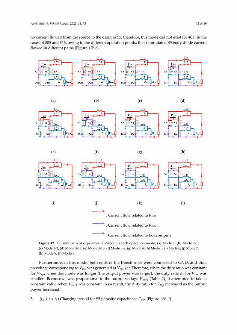
World Electric Vehicle Journal 2020, 11, 78 12 of 19
no current flowed from the source to the drain in S5; therefore, this mode did not exist for #01. In thecases of #05 and #16, owing to the different operation points, the commutated S5 body diode currentflowed in different paths (Figure 12b,c).
World Electric Vehicle Journal 2020, 11, x; doi: www.mdpi.com/journal/wevj
(a)
(b)
(c)
L11
L12
L21
L22
Vtxs
S5 S6
D1 D2 Rout1Rout2
(d)
(e)
(f)
(g)
(h)
(i)
L11
L12
L21
L22
Vtxs
S5 S6
D1 D2 Rout1Rout2
(j)
(k)
(l)
: Current flow related to Rout1
: Current flow related to Rout2
: Current flow related to both outputs
Figure 12. Current path of experimental circuit in each operation mode; (a) Mode 1; (b) Mode 2-1; (c) Mode 2-2; (d) Mode 3-1a; (e) Mode 3-1b; (f) Mode 3-2; (g) Mode 4; (h) Mode 5; (i) Mode 6; (j) Mode 7; (k) Mode 8; (l) Mode 9.
Figure 12. Current path of experimental circuit in each operation mode; (a) Mode 1; (b) Mode 2-1;(c) Mode 2-2; (d) Mode 3-1a; (e) Mode 3-1b; (f) Mode 3-2; (g) Mode 4; (h) Mode 5; (i) Mode 6; (j) Mode 7;(k) Mode 8; (l) Mode 9.
Furthermore, in this mode, both ends of the transformer were connected to GND, and thus,no voltage corresponding to Vtxp was generated at Vtxs yet. Therefore, when the duty ratio was constantfor Vtxp, when this mode was longer (the output power was larger), the duty ratio d1 for Vtxs wassmaller. Because d1 was proportional to the output voltage Vout1 (Table 2), it attempted to take aconstant value when Vout1 was constant. As a result, the duty ratio for Vtxp increased as the outputpower increased.
3. (t3 < t < t5) Charging period for S5 parasitic capacitance Cds5 (Figure 12d–f).

World Electric Vehicle Journal 2020, 11, 78 13 of 19
The S5 body diode current became zero and Vtxs started to rise. This Vtxs acted as a power sourceto charge Cds5 (Figure 12d,f). This charging current was the peak current of Itxs and the current changegenerated a surge voltage at Vds5. As described later, this noise propagated to the entire secondaryside circuit, including Vgs5 and Vgs6. A larger Pout2 resulted in a larger rate of change in the current.Therefore, the peak surge voltage was greater for #16 than for #01 and #05. Moreover, because the L21current (D1 current) in the previous mode was small for #01 and #05, the charging current for Cds5
flowed to not only L21, but also to D1, causing the charging (t3 < t < t4) and discharging (t4 < t < t5) ofthe D1 parasitic capacitance CD1 (Figure 12d,e). This charging and discharging generated a voltage ofapproximately 70 V at Vdiode1. However, for #16, the D1 current in the previous mode was sufficientlylarge, and thus, the charging current for Cds5 did not charge CD1 (Figure 12f).
4. (t5 < t < t6) Period corresponding to ideal operation mode 1 (Figure 12g).
S5 was off and D1 was on, and it operated in mode 1 of the ideal operation principle.
5. (t6 < t < t7) Discharging period for Cds5 (Figure 12h).
Discharging of Cds5 was caused by turning on Vgs5, when the current flowing to L21 started toswitch from the D1 current to the S5 current. The current continued to flow into S5 and D1 until S5 wason and completely switched; therefore, both ends of Vtxs were connected to GND again, reducing Vtxs.
6. (t7 < t < t8) Charging period for CD1 (Figure 12i).
Once the discharging of Cds5 was complete and S5 was completely on, the current started to flowto L21 via S5. At the same time, the charging of CD1 started to turn off D1. The peak for Itxs was thecharging current. The current change at this point generated a surge voltage at Vdiode1. The periodst6 to t8 were the time from the start of discharging Cds5 until the end of charging CD1. The currentinvolved in the charging and discharging was dependent on Pout2. Consequently, #16, with a greaterPout2, had a longer t6 to t8 period than #01 and #05.
7. (t8 < t < t9) Period corresponding to ideal operation mode 2 (Figure 12j).
D1 was completely off and it operated in mode 2 of the ideal operation principle.
8. (t9 < t < t10) Discharging period for CD1 (Figure 12k).
By switching the primary side inverter, Vtxp and Vtxs decreased simultaneously. Accordingly,the current flowing from the transformer to L21 decreased. To compensate for this current loss, D1 wasturned on. Discharging of CD1 occurred as a preliminary step.
9. (t10 < t < t11) Period corresponding to ideal operation mode 3 (Figure 12l).
D1 was completely on, and it operated in mode 3 of the ideal operation principle.The following half cycle behaved symmetrically with the nine modes described thus far.
The behavior at each operation point during steady-state operation has been described with theseries of operation modes above.
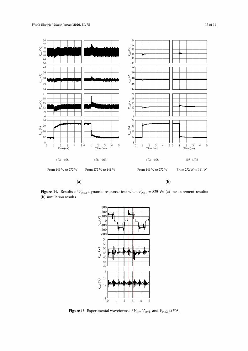
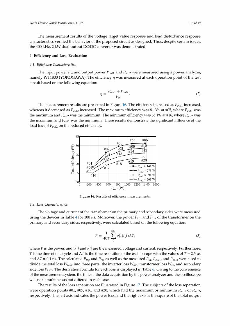
3.7. Load Disturbance Response Characteristics
Figures 13 and 14 present the actual measurement results and simulation results of Vout1, Iout1,Vout2, and Iout2 when the operation point was switched during steady-state operation. Figure 15 showsthe waveforms of Vtxs, Vout1, and Vout2 at operation point #08. In Figure 13, operation points #02 and#03 were switched to switch Pout1 only. In Figure 14, #03 and #08 were switched to switch Pout2 only.PSIM version 12.04 (Powersim) was used for the simulation. The parameters in Table 3 were used inthe simulation, and an ideal device was assumed for the switching devices. Furthermore, no parasitic
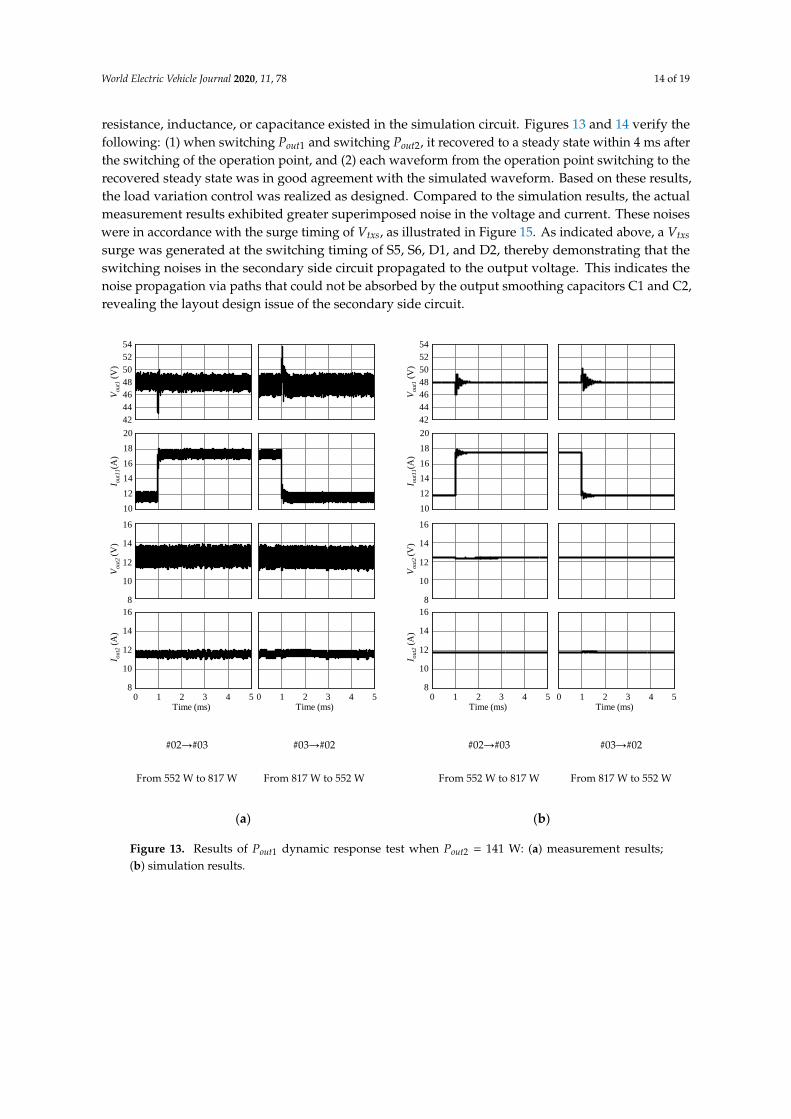
World Electric Vehicle Journal 2020, 11, 78 14 of 19
resistance, inductance, or capacitance existed in the simulation circuit. Figures 13 and 14 verify thefollowing: (1) when switching Pout1 and switching Pout2, it recovered to a steady state within 4 ms afterthe switching of the operation point, and (2) each waveform from the operation point switching to therecovered steady state was in good agreement with the simulated waveform. Based on these results,the load variation control was realized as designed. Compared to the simulation results, the actualmeasurement results exhibited greater superimposed noise in the voltage and current. These noiseswere in accordance with the surge timing of Vtxs, as illustrated in Figure 15. As indicated above, a Vtxs
surge was generated at the switching timing of S5, S6, D1, and D2, thereby demonstrating that theswitching noises in the secondary side circuit propagated to the output voltage. This indicates thenoise propagation via paths that could not be absorbed by the output smoothing capacitors C1 and C2,revealing the layout design issue of the secondary side circuit.
World Electric Vehicle Journal 2020, 11, x 14 of 20
3.7. Load Disturbance Response Characteristics
Figures 13 and 14 present the actual measurement results and simulation results of Vout1, Iout1, Vout2,
and Iout2 when the operation point was switched during steady-state operation. Figure 15 shows the
waveforms of Vtxs, Vout1, and Vout2 at operation point #08. In Figure 13, operation points #02 and #03
were switched to switch Pout1 only. In Figure 14, #03 and #08 were switched to switch Pout2 only. PSIM
version 12.04 (Powersim) was used for the simulation. The parameters in Table 3 were used in the
simulation, and an ideal device was assumed for the switching devices. Furthermore, no parasitic
resistance, inductance, or capacitance existed in the simulation circuit. Figures 13 and 14 verify the
following: (1) when switching Pout1 and switching Pout2, it recovered to a steady state within 4 ms after
the switching of the operation point, and (2) each waveform from the operation point switching to
the recovered steady state was in good agreement with the simulated waveform. Based on these
results, the load variation control was realized as designed. Compared to the simulation results, the
actual measurement results exhibited greater superimposed noise in the voltage and current. These
noises were in accordance with the surge timing of Vtxs, as illustrated in Figure 15. As indicated above,
a Vtxs surge was generated at the switching timing of S5, S6, D1, and D2, thereby demonstrating that
the switching noises in the secondary side circuit propagated to the output voltage. This indicates the
noise propagation via paths that could not be absorbed by the output smoothing capacitors C1 and
C2, revealing the layout design issue of the secondary side circuit.
#02→#03
From 552 W to 817 W
#03→#02
From 817 W to 552 W
#02→#03
From 552 W to 817 W
#03→#02
From 817 W to 552 W
(a) (b)
Figure 13. Results of Pout1 dynamic response test when Pout2 = 141 W: (a) measurement results; (b)
simulation results.
42
44
46
48
50
52
54
10
12
14
16
18
20
8
10
12
14
16
0 1 2 3 4 58
10
12
14
16
Vout1
(V
)I o
ut1
1(A
)V
out2
(V
)I o
ut2
(A
)
Time (ms)
42
44
46
48
50
52
54
10
12
14
16
18
20
8
10
12
14
16
0 1 2 3 4 58
10
12
14
16
Vo
ut1
(V
)I o
ut1
1(A
)V
ou
t2 (
V)
I ou
t2 (
A)
Time (ms)
42
44
46
48
50
52
54
10
12
14
16
18
20
8
10
12
14
16
0 1 2 3 4 58
10
12
14
16
Vo
ut1
(V
)I o
ut1
1(A
)V
ou
t2 (
V)
I ou
t2 (
A)
Time (ms)
42
44
46
48
50
52
54
10
12
14
16
18
20
8
10
12
14
16
0 1 2 3 4 58
10
12
14
16
Vo
ut1
(V
)I o
ut1
1(A
)V
ou
t2 (
V)
I ou
t2 (
A)
Time (ms)
Figure 13. Results of Pout1 dynamic response test when Pout2 = 141 W: (a) measurement results;(b) simulation results.
World Electric Vehicle Journal 2020, 11, 78 15 of 19
World Electric Vehicle Journal 2020, 11, x 15 of 20
#03→#08
From 141 W to 272 W
#08→#03
From 272 W to 141 W
#03→#08
From 141 W to 272 W
#08→#03
From 272 W to 141 W
(a) (b)
Figure 14. Results of Pout2 dynamic response test when Pout1 = 825 W: (a) measurement results; (b)
simulation results.
Figure 15. Experimental waveforms of Vtxs, Vout1, and Vout2 at #08.
42
44
46
48
50
52
54
14
16
18
20
22
6
9
12
15
18
21
0 1 2 3 4 58
12
16
20
24
Vout1
(V
)I o
ut1
1(A
)V
out2
(V
)I o
ut2
(A
)
Time (ms)
42
44
46
48
50
52
54
14
16
18
20
22
6
9
12
15
18
21
0 1 2 3 4 58
12
16
20
24
Vou
t1 (
V)
I ou
t11(A
)V
out2
(V
)I o
ut2
(A
)
Time (ms)
44
46
48
50
52
54
14
16
18
20
22
6
9
12
15
18
21
0 1 2 3 4 58
12
16
20
24
Vo
ut1
(V
)I o
ut1
1(A
)V
ou
t2 (
V)
I ou
t2 (
A)
Time (ms)
44
46
48
50
52
54
14
16
18
20
22
6
9
12
15
18
21
0 1 2 3 4 58
12
16
20
24
Vo
ut1
(V
)I o
ut1
1(A
)V
ou
t2 (
V)
I ou
t2 (
A)
Time (ms)
42
44
46
48
50
52
54
-300
-200
-100
0
100
200
300
0 1 2 3 4 58
10
12
14
16
Vo
ut1
(V
)V
txs
(V)
Vo
ut2
(V
)
Figure 14. Results of Pout2 dynamic response test when Pout1 = 825 W: (a) measurement results;(b) simulation results.
World Electric Vehicle Journal 2020, 11, x 15 of 20
#03→#08
From 141 W to 272 W
#08→#03
From 272 W to 141 W
#03→#08
From 141 W to 272 W
#08→#03
From 272 W to 141 W
(a) (b)
Figure 14. Results of Pout2 dynamic response test when Pout1 = 825 W: (a) measurement results; (b)
simulation results.
Figure 15. Experimental waveforms of Vtxs, Vout1, and Vout2 at #08.
42
44
46
48
50
52
54
14
16
18
20
22
6
9
12
15
18
21
0 1 2 3 4 58
12
16
20
24
Vout1
(V
)I o
ut1
1(A
)V
out2
(V
)I o
ut2
(A
)
Time (ms)
42
44
46
48
50
52
54
14
16
18
20
22
6
9
12
15
18
21
0 1 2 3 4 58
12
16
20
24
Vou
t1 (
V)
I ou
t11(A
)V
out2
(V
)I o
ut2
(A
)
Time (ms)
44
46
48
50
52
54
14
16
18
20
22
6
9
12
15
18
21
0 1 2 3 4 58
12
16
20
24
Vo
ut1
(V
)I o
ut1
1(A
)V
ou
t2 (
V)
I ou
t2 (
A)
Time (ms)
44
46
48
50
52
54
14
16
18
20
22
6
9
12
15
18
21
0 1 2 3 4 58
12
16
20
24
Vo
ut1
(V
)I o
ut1
1(A
)V
ou
t2 (
V)
I ou
t2 (
A)
Time (ms)
42
44
46
48
50
52
54
-300
-200
-100
0
100
200
300
0 1 2 3 4 58
10
12
14
16
Vo
ut1
(V
)V
txs
(V)
Vo
ut2
(V
)
Figure 15. Experimental waveforms of Vtxs, Vout1, and Vout2 at #08.
World Electric Vehicle Journal 2020, 11, 78 16 of 19
The measurement results of the voltage target value response and load disturbance responsecharacteristics verified the behavior of the proposed circuit as designed. Thus, despite certain issues,the 400 kHz, 2 kW dual-output DC/DC converter was demonstrated.
4. Efficiency and Loss Evaluation
4.1. Efficiency Characteristics
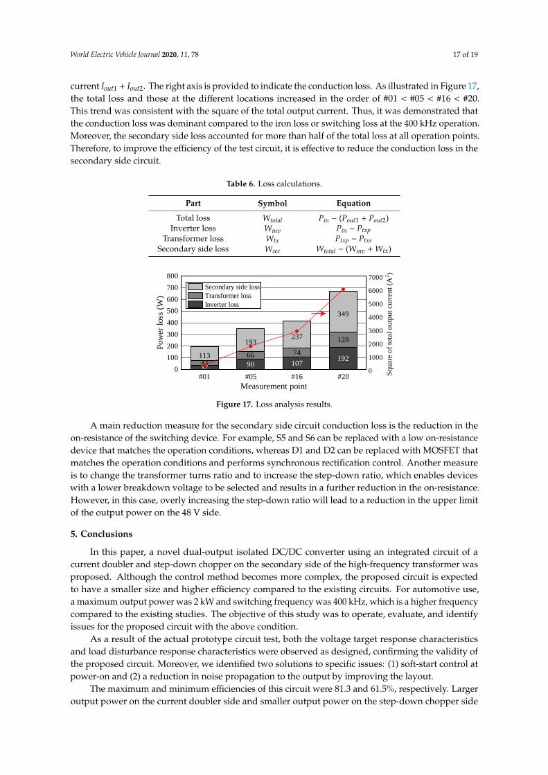
The input power Pin and output power Pout1 and Pout2 were measured using a power analyzer,namely WT1800 (YOKOGAWA). The efficiency η was measured at each operation point of the testcircuit based on the following equation:
η =Pout1 + Pout2
Pin. (2)
The measurement results are presented in Figure 16. The efficiency increased as Pout1 increased,whereas it decreased as Pout2 increased. The maximum efficiency was 81.3% at #05, where Pout1 wasthe maximum and Pout2 was the minimum. The minimum efficiency was 65.1% at #16, where Pout2 wasthe maximum and Pout1 was the minimum. These results demonstrate the significant influence of theload loss of Pout2 on the reduced efficiency.
World Electric Vehicle Journal 2020, 11, x 16 of 20
The measurement results of the voltage target value response and load disturbance response
characteristics verified the behavior of the proposed circuit as designed. Thus, despite certain issues,
the 400 kHz, 2 kW dual-output DC/DC converter was demonstrated.
4. Efficiency and Loss Evaluation
4.1. Efficiency Characteristics
The input power Pin and output power Pout1 and Pout2 were measured using a power analyzer,
namely WT1800 (YOKOGAWA). The efficiency η was measured at each operation point of the test
circuit based on the following equation:
η =Pout1 + Pout2
Pin. (2)
The measurement results are presented in Figure 16. The efficiency increased as Pout1 increased,
whereas it decreased as Pout2 increased. The maximum efficiency was 81.3% at #05, where Pout1 was
the maximum and Pout2 was the minimum. The minimum efficiency was 65.1% at #16, where Pout2 was
the maximum and Pout1 was the minimum. These results demonstrate the significant influence of the
load loss of Pout2 on the reduced efficiency.
Figure 16. Results of efficiency measurements.
4.2. Loss Characteristics
The voltage and current of the transformer on the primary and secondary sides were measured
using the devices in Table 4 for 100 μs. Moreover, the power Ptxp and Ptxs of the transformer on the
primary and secondary sides, respectively, were calculated based on the following equation:
𝑃 =1
40T∑ v(t)i(t)T
40T
0
, (3)
where P is the power, and v(t) and i(t) are the measured voltage and current, respectively.
Furthermore, T is the time of one cycle and ∆T is the time resolution of the oscilloscope with the
values of T = 2.5 μs and ∆T = 0.1 ns. The calculated Ptxp and Ptxs as well as the measured Pin, Pout1, and
Pout2 were used to divide the total loss Wtotal into three parts: the inverter loss Winv, transformer loss
Wtx, and secondary side loss Wsec. The derivation formula for each loss is displayed in Table 6. Owing
to the convenience of the measurement system, the time of the data acquisition by the power analyzer
and the oscilloscope was not simultaneous but differed in each case.
0 200 400 600 800 1000 1200 1400 160060
65
70
75
80
85
#
To
tal
effi
cien
cy (
%)
Pout1 (W)
Pout2 ≈ 141 W
Pout2 ≈ 273 W
Pout2 ≈ 394 W
Pout2 ≈ 501 W
#02
#03#04 #05
#06
#07
#08#09 #10
#11
#12
#15#13
#14
#16
#17
#18#20
#01#19
Figure 16. Results of efficiency measurements.
4.2. Loss Characteristics
The voltage and current of the transformer on the primary and secondary sides were measuredusing the devices in Table 4 for 100 µs. Moreover, the power Ptxp and Ptxs of the transformer on theprimary and secondary sides, respectively, were calculated based on the following equation:
P =1
40T
40T∑0
v(t)i(t)∆T, (3)
where P is the power, and v(t) and i(t) are the measured voltage and current, respectively. Furthermore,T is the time of one cycle and ∆T is the time resolution of the oscilloscope with the values of T = 2.5 µsand ∆T = 0.1 ns. The calculated Ptxp and Ptxs as well as the measured Pin, Pout1, and Pout2 were used todivide the total loss Wtotal into three parts: the inverter loss Winv, transformer loss Wtx, and secondaryside loss Wsec. The derivation formula for each loss is displayed in Table 6. Owing to the convenienceof the measurement system, the time of the data acquisition by the power analyzer and the oscilloscopewas not simultaneous but differed in each case.
The results of the loss separation are illustrated in Figure 17. The subjects of the loss separationwere operation points #01, #05, #16, and #20, which had the maximum or minimum Pout1 or Pout2,respectively. The left axis indicates the power loss, and the right axis is the square of the total output
World Electric Vehicle Journal 2020, 11, 78 17 of 19
current Iout1 + Iout2. The right axis is provided to indicate the conduction loss. As illustrated in Figure 17,the total loss and those at the different locations increased in the order of #01 < #05 < #16 < #20.This trend was consistent with the square of the total output current. Thus, it was demonstrated thatthe conduction loss was dominant compared to the iron loss or switching loss at the 400 kHz operation.Moreover, the secondary side loss accounted for more than half of the total loss at all operation points.Therefore, to improve the efficiency of the test circuit, it is effective to reduce the conduction loss in thesecondary side circuit.
Table 6. Loss calculations.
Part Symbol Equation
Total loss Wtotal Pin − (Pout1 + Pout2)Inverter loss Winv Pin − Ptxp
Transformer loss Wtx Ptxp − PtxsSecondary side loss Wsec Wtotal − (Winv + Wtx)
World Electric Vehicle Journal 2020, 11, x 17 of 20
Table 6. Loss calculations.
Part Symbol Equation
Total loss Wtotal Pin − (Pout1 + Pout2)
Inverter loss Winv Pin − Ptxp
Transformer loss Wtx Ptxp − Ptxs
Secondary side loss Wsec Wtotal − (Winv+ Wtx)
The results of the loss separation are illustrated in Figure 17. The subjects of the loss separation
were operation points #01, #05, #16, and #20, which had the maximum or minimum Pout1 or Pout2,
respectively. The left axis indicates the power loss, and the right axis is the square of the total output
current Iout1 + Iout2. The right axis is provided to indicate the conduction loss. As illustrated in Figure
17, the total loss and those at the different locations increased in the order of #01 < #05 < #16 < #20.
This trend was consistent with the square of the total output current. Thus, it was demonstrated that
the conduction loss was dominant compared to the iron loss or switching loss at the 400 kHz
operation. Moreover, the secondary side loss accounted for more than half of the total loss at all
operation points. Therefore, to improve the efficiency of the test circuit, it is effective to reduce the
conduction loss in the secondary side circuit.
Figure 17. Loss analysis results.
A main reduction measure for the secondary side circuit conduction loss is the reduction in the
on-resistance of the switching device. For example, S5 and S6 can be replaced with a low on-resistance
device that matches the operation conditions, whereas D1 and D2 can be replaced with MOSFET that
matches the operation conditions and performs synchronous rectification control. Another measure
is to change the transformer turns ratio and to increase the step-down ratio, which enables devices
with a lower breakdown voltage to be selected and results in a further reduction in the on-resistance.
However, in this case, overly increasing the step-down ratio will lead to a reduction in the upper
limit of the output power on the 48 V side.
5. Conclusions
In this paper, a novel dual-output isolated DC/DC converter using an integrated circuit of a
current doubler and step-down chopper on the secondary side of the high-frequency transformer
was proposed. Although the control method becomes more complex, the proposed circuit is expected
to have a smaller size and higher efficiency compared to the existing circuits. For automotive use, a
maximum output power was 2 kW and switching frequency was 400 kHz, which is a higher
frequency compared to the existing studies. The objective of this study was to operate, evaluate, and
identify issues for the proposed circuit with the above condition.
37 90 107192
4366 74
128
113
193237
349
#01 #05 #16 #200
100
200
300
400
500
600
700
800
Sq
uar
e o
f to
tal
ou
tpu
t cu
rren
t (A
2)
Pow
er l
oss
(W
)
Measurement point
Secondary side loss
Transformer loss
Inverter loss
0
1000
2000
3000
4000
5000
6000
7000
Figure 17. Loss analysis results.
A main reduction measure for the secondary side circuit conduction loss is the reduction in theon-resistance of the switching device. For example, S5 and S6 can be replaced with a low on-resistancedevice that matches the operation conditions, whereas D1 and D2 can be replaced with MOSFET thatmatches the operation conditions and performs synchronous rectification control. Another measureis to change the transformer turns ratio and to increase the step-down ratio, which enables deviceswith a lower breakdown voltage to be selected and results in a further reduction in the on-resistance.However, in this case, overly increasing the step-down ratio will lead to a reduction in the upper limitof the output power on the 48 V side.
5. Conclusions
In this paper, a novel dual-output isolated DC/DC converter using an integrated circuit of acurrent doubler and step-down chopper on the secondary side of the high-frequency transformer wasproposed. Although the control method becomes more complex, the proposed circuit is expectedto have a smaller size and higher efficiency compared to the existing circuits. For automotive use,a maximum output power was 2 kW and switching frequency was 400 kHz, which is a higher frequencycompared to the existing studies. The objective of this study was to operate, evaluate, and identifyissues for the proposed circuit with the above condition.
As a result of the actual prototype circuit test, both the voltage target response characteristicsand load disturbance response characteristics were observed as designed, confirming the validity ofthe proposed circuit. Moreover, we identified two solutions to specific issues: (1) soft-start control atpower-on and (2) a reduction in noise propagation to the output by improving the layout.
The maximum and minimum efficiencies of this circuit were 81.3 and 61.5%, respectively. Largeroutput power on the current doubler side and smaller output power on the step-down chopper side
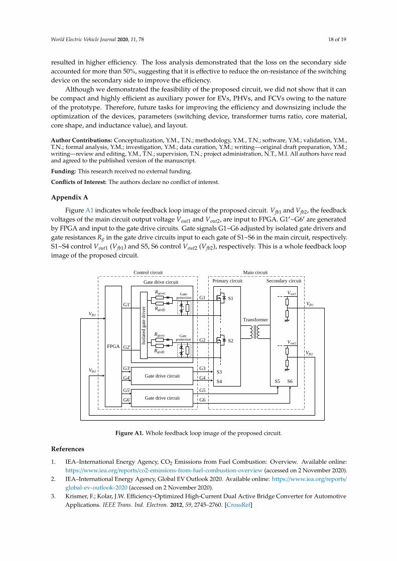
World Electric Vehicle Journal 2020, 11, 78 18 of 19
resulted in higher efficiency. The loss analysis demonstrated that the loss on the secondary sideaccounted for more than 50%, suggesting that it is effective to reduce the on-resistance of the switchingdevice on the secondary side to improve the efficiency.
Although we demonstrated the feasibility of the proposed circuit, we did not show that it canbe compact and highly efficient as auxiliary power for EVs, PHVs, and FCVs owing to the natureof the prototype. Therefore, future tasks for improving the efficiency and downsizing include theoptimization of the devices, parameters (switching device, transformer turns ratio, core material,core shape, and inductance value), and layout.
Author Contributions: Conceptualization, Y.M., T.N.; methodology, Y.M., T.N.; software, Y.M.; validation, Y.M.,T.N.; formal analysis, Y.M.; investigation, Y.M.; data curation, Y.M.; writing—original draft preparation, Y.M.;writing—review and editing, Y.M., T.N.; supervision, T.N.; project administration, N.T., M.I. All authors have readand agreed to the published version of the manuscript.
Funding: This research received no external funding.
Conflicts of Interest: The authors declare no conflict of interest.
Appendix A
Figure A1 indicates whole feedback loop image of the proposed circuit. Vfb1 and Vfb2, the feedbackvoltages of the main circuit output voltage Vout1 and Vout2, are input to FPGA. G1′~G6′ are generatedby FPGA and input to the gate drive circuits. Gate signals G1~G6 adjusted by isolated gate drivers andgate resistances Rg in the gate drive circuits input to each gate of S1~S6 in the main circuit, respectively.S1~S4 control Vout1 (Vfb1) and S5, S6 control Vout2 (Vfb2), respectively. This is a whole feedback loopimage of the proposed circuit.
World Electric Vehicle Journal 2020, 11, x 18 of 20
As a result of the actual prototype circuit test, both the voltage target response characteristics
and load disturbance response characteristics were observed as designed, confirming the validity of
the proposed circuit. Moreover, we identified two solutions to specific issues: (1) soft-start control at
power-on and (2) a reduction in noise propagation to the output by improving the layout.
The maximum and minimum efficiencies of this circuit were 81.3 and 61.5%, respectively. Larger
output power on the current doubler side and smaller output power on the step-down chopper side
resulted in higher efficiency. The loss analysis demonstrated that the loss on the secondary side
accounted for more than 50%, suggesting that it is effective to reduce the on-resistance of the
switching device on the secondary side to improve the efficiency.
Although we demonstrated the feasibility of the proposed circuit, we did not show that it can
be compact and highly efficient as auxiliary power for EVs, PHVs, and FCVs owing to the nature of
the prototype. Therefore, future tasks for improving the efficiency and downsizing include the
optimization of the devices, parameters (switching device, transformer turns ratio, core material, core
shape, and inductance value), and layout.
Author Contributions: Conceptualization, Y.M., T.N.; methodology, Y.M., T.N.; software, Y.M.; validation, Y.M.,
T.N.; formal analysis, Y.M.; investigation, Y.M.; data curation, Y.M.; writing—original draft preparation, Y.M.;
writing—review and editing, Y.M., T.N.; supervision, T.N.; project administration, N.T., M.I. All authors have
read and agreed to the published version of the manuscript.
Funding: This research received no external funding.
Conflicts of Interest: The authors declare no conflict of interest.
Appendix A
Figure A1 indicates whole feedback loop image of the proposed circuit. Vfb1 and Vfb2, the feedback
voltages of the main circuit output voltage Vout1 and Vout2, are input to FPGA. G1′~G6′ are generated
by FPGA and input to the gate drive circuits. Gate signals G1~G6 adjusted by isolated gate drivers
and gate resistances Rg in the gate drive circuits input to each gate of S1~S6 in the main circuit,
respectively. S1~S4 control Vout1 (Vfb1) and S5, S6 control Vout2 (Vfb2), respectively. This is a whole
feedback loop image of the proposed circuit.
Vfb1
Vfb2
S1
Iso
late
d g
ate
dri
ver
Gate drive circuit
S2
Main circuitControl circuit
Gate drive circuit
Gate drive circuitS3
S4 S5 S6
G1'
G2'
G3'
G4'
G5'
G6'
G1
G2
G3
G4
G5
G6
Vfb1
Vfb2
Rg(on)
Rg(off)
Rg(on)
Rg(off)
FPGA
protectionGate
protectionGate Vout1
Primary circuit
Transformer
Secondary circuit
Vout2
Figure A1. Whole feedback loop image of the proposed circuit.
Figure A1. Whole feedback loop image of the proposed circuit.
References
1. IEA–International Energy Agency, CO2 Emissions from Fuel Combustion: Overview. Available online:https://www.iea.org/reports/co2-emissions-from-fuel-combustion-overview (accessed on 2 November 2020).
2. IEA–International Energy Agency, Global EV Outlook 2020. Available online: https://www.iea.org/reports/global-ev-outlook-2020 (accessed on 2 November 2020).
3. Krismer, F.; Kolar, J.W. Efficiency-Optimized High-Current Dual Active Bridge Converter for AutomotiveApplications. IEEE Trans. Ind. Electron. 2012, 59, 2745–2760. [CrossRef]

World Electric Vehicle Journal 2020, 11, 78 19 of 19
4. Hou, R.; Magne, P.; Bilgin, B.; Emadi, A. A topological evaluation of isolated DC/DC converters for AuxiliaryPower Modules in Electrified Vehicle applications. In Proceedings of the 2015 IEEE Applied Power ElectronicsConference and Exposition (APEC), Charlotte, NC, USA, 15–19 March 2015.
5. Rhodes, K.; Kok, D.; Sohoni, P.; Perry, E.; Kraska, M.; Wallace, M. Estimation of the Effects of AuxiliaryElectrical Loads on Hybrid Electric Vehicle Fuel Economy. SAE Tech. Pap. 2017, 1, 1155.
6. Adriano, S.; Chiara, F.; Fabrizio, Z.; Alessandro, D.; Fabio, O.; Annalisa, D. Experimental Analysis of theAuxiliaries Consumption in the Energy Balance of a Pre-series Plug-in Hybrid-electric Vehicle. Energy Procedia2014, 45, 779–788. [CrossRef]
7. Teratani, T. Impact of DC48V on Automotive Power Supply Systems—Comparison with DC42V and FutureView under DC60V—. IEEJ Trans. Ind. Appl. 2015, 135, 892–897. [CrossRef]
8. Hayslett, S.; Maanen, K.V.; Wenzel, W.; Husain, T. The 48-V Mild Hybrid: Benefits, Motivation, and theFuture Outlook. IEEE Electrif. Mag. 2020, 8, 11–17. [CrossRef]
9. Chen, G.; Deng, Y.; Dong, J.; Hu, Y.; Jiang, L.; He, X. Integrated Multiple-Output Synchronous Buck Converterfor Electric Vehicle Power Supply. IEEE Trans. Veh. Technol. 2017, 66, 5752–5761. [CrossRef]
10. Matsushita, Y.; Noguchi, T.; Kimura, O.; Sunayama, T. Current-doubler based multiport DC/DC converterwith galvanic isolation. In Proceedings of the 2017 IEEE 12th International Conference on Power Electronicsand Drive Systems (PEDS), Honolulu, HI, USA, 12–15 December 2017.
11. Jones, E.A.; de Rooij, M.; Biswas, S. GaN Based DC-DC Converter for 48 V Automotive Applications.In Proceedings of the 2019 IEEE Workshop on Wide Bandgap Power Devices and Applications in Asia(WiPDA Asia), Taipei, Taiwan, 23–25 May 2019.
12. Martinez-heredia, J., M.; Colodro, F.; Mora-Jiménez, J.L.; Remujo, A.; Soriano, J.; Esteban, S. Development ofGaN Technology-Based DC/DC Converter for Hybrid UAV. IEEE Access 2020, 8, 88014–88025. [CrossRef]
13. Mitova, R.; Ghosh, R.; Mhaskar, U.; Klikic, D.; Wang, M.; Dentella, A. Investigations of 600-V GaN HEMT andGaN Diode for Power Converter Applications. IEEE Trans. Power Electron. 2014, 29, 2441–2452. [CrossRef]
14. Huang, X.; Lee, F.C.; Li, Q.; Du, W. High-Efficiency GaN-Based Interleaved CRM Bidirectional Buck/BoostConverter with Inverse Coupled Inductor. IEEE Trans. Power Electron. 2016, 31, 4343–4352. [CrossRef]
15. Imaoka, J.; Okamoto, K.; Kimura, S.; Noah, M.; Martinez, W.; Yamamoto, M.; Shoyama, M. A Magnetic DesignMethod Considering DC-Biased Magnetization for Integrated Magnetic Components Used in MultiphaseBoost Converters. IEEE Trans. Power Electron. 2018, 33, 3346–3362. [CrossRef]
16. Sugimura, K.; Yabu, N.; Sonehara, M.; Sato, T. Novel Method for Making Surface Insulation Layer onFe-Based Amorphous Alloy Powder by Surface-Modification Using Two-Step Acid Solution Processing.IEEE Trans. Magn. 2018, 54, 2801805. [CrossRef]
17. Liang, W.; Raymond, L.; Rivas, J. 3-D-Printed Air-Core Inductors for High-Frequency Power Converters.IEEE Trans. Power Electron. 2016, 31, 52–64. [CrossRef]
18. Inoue, S.; Itoh, K.; Ishigaki, M.; Sugiyama, T. Magnetically integrated isolated bidirectional three-port DC-DCconverter. In Proceedings of the 2017 19th European Conference on Power Electronics and Applications(EPE’17 ECCE Europe), Warsaw, Poland, 11–14 September 2017.
19. Dao, N.D.; Lee, D.; Phan, Q.D. High-Efficiency SiC-Based Isolated Three-Port DC/DC Converters for HybridCharging Stations. IEEE Trans. Power Electron. 2020, 35, 10455–10465. [CrossRef]
20. Tang, Y.; Lu, J.; Wu, B.; Zou, S.; Ding, W.; Khaligh, A. An Integrated Dual-Output Isolated Converter forPlug-in Electric Vehicles. IEEE Trans. Veh. Technol. 2018, 67, 966–976. [CrossRef]
Publisher’s Note: MDPI stays neutral with regard to jurisdictional claims in published maps and institutionalaffiliations.
© 2020 by the authors. Licensee MDPI, Basel, Switzerland. This article is an open accessarticle distributed under the terms and conditions of the Creative Commons Attribution(CC BY) license (http://creativecommons.org/licenses/by/4.0/).


