Embed Size (px)
Citation preview
Power Supply Design Seminar
Bi-directional DC/DC converter topology comparison and design
Reproduced from 2016 Texas Instruments Power Supply Design Seminar SEM2200
TI Literature Number: SLUP343 © 2016, 2017 Texas Instruments Incorporated
Power Seminar topics and online power training modules are available at:ti.com/psds
Texas Instruments – 2016/17 Power Supply Design Seminar
Bi-directional DC/DC converter topology comparison and design
HEV/EV and server applications
Sanatan RajagopalanZhong Ye
Texas Instruments – 2016/17 Power Supply Design SeminarTexas Instruments – 2016/17 Power Supply Design Seminar
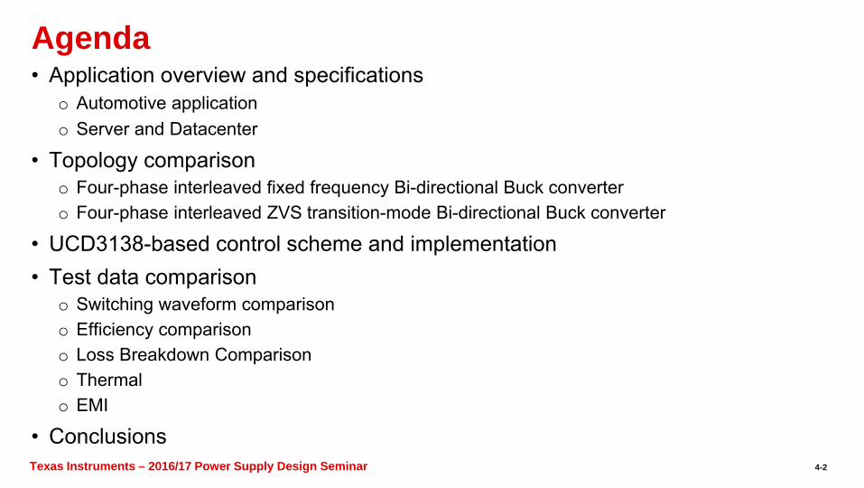
Agenda• Application overview and specifications
o Automotive applicationo Server and Datacenter
• Topology comparisono Four-phase interleaved fixed frequency Bi-directional Buck convertero Four-phase interleaved ZVS transition-mode Bi-directional Buck converter
• UCD3138-based control scheme and implementation • Test data comparison
o Switching waveform comparisono Efficiency comparisono Loss Breakdown Comparisono Thermal o EMI
• Conclusions4-2
Texas Instruments – 2016/17 Power Supply Design SeminarTexas Instruments – 2016/17 Power Supply Design Seminar
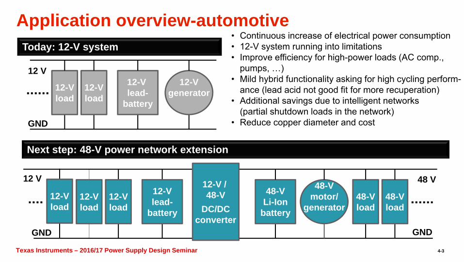
Application overview-automotive• Continuous increase of electrical power consumption• 12-V system running into limitations • Improve efficiency for high-power loads (AC comp.,
pumps, …)• Mild hybrid functionality asking for high cycling perform-
ance (lead acid not good fit for more recuperation)• Additional savings due to intelligent networks
(partial shutdown loads in the network)• Reduce copper diameter and cost
12-V lead-
battery
12-Vload
12-Vgenerator12-V
load
12 V
GND
Today: 12-V system
12 V
GND
48-VLi-Ion
battery
48-Vmotor/
generator
12-V / 48-V
DC/DCconverter
48 V
GND
48-Vload
48-Vload
Next step: 48-V power network extension
12-Vlead-
battery
12-Vload
12-Vload
12-Vload
4-3
Texas Instruments – 2016/17 Power Supply Design SeminarTexas Instruments – 2016/17 Power Supply Design Seminar
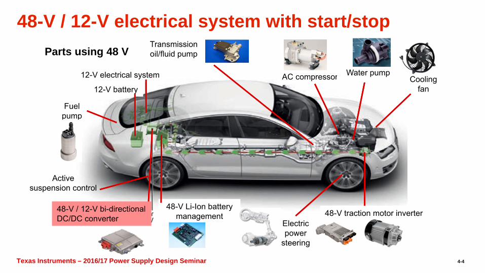
48-V / 12-V electrical system with start/stop
12-V electrical system
12-V battery
48-V Li-Ion battery management 48-V traction motor inverter
Activesuspension control
AC compressor Water pump
Electricpower
steering
Coolingfan
Transmissionoil/fluid pump
Fuelpump
Parts using 48 V
48-V / 12-V bi-directionalDC/DC converter
4-4
Texas Instruments – 2016/17 Power Supply Design SeminarTexas Instruments – 2016/17 Power Supply Design Seminar
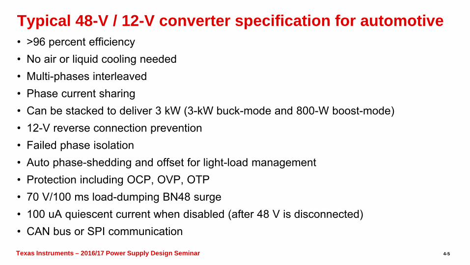
Typical 48-V / 12-V converter specification for automotive• >96 percent efficiency• No air or liquid cooling needed• Multi-phases interleaved • Phase current sharing• Can be stacked to deliver 3 kW (3-kW buck-mode and 800-W boost-mode)• 12-V reverse connection prevention • Failed phase isolation• Auto phase-shedding and offset for light-load management• Protection including OCP, OVP, OTP• 70 V/100 ms load-dumping BN48 surge • 100 uA quiescent current when disabled (after 48 V is disconnected)• CAN bus or SPI communication
4-5
Texas Instruments – 2016/17 Power Supply Design SeminarTexas Instruments – 2016/17 Power Supply Design Seminar
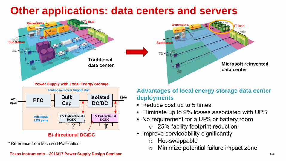
Microsoft reinvented data center
Traditional data center
Bi-directional DC/DC
Advantages of local energy storage data center deployments• Reduce cost up to 5 times• Eliminate up to 9% losses associated with UPS• No requirement for a UPS or battery room
o 25% facility footprint reduction• Improve serviceability significantly
o Hot-swappable o Minimize potential failure impact zone
Other applications: data centers and servers
* Reference from Microsoft Publication
Generators
UPS
IT load
Substation Substation
IT loadGenerators
4-6
Texas Instruments – 2016/17 Power Supply Design SeminarTexas Instruments – 2016/17 Power Supply Design Seminar
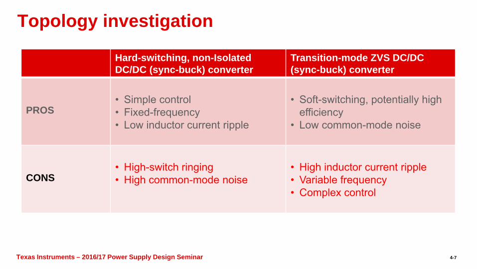
Topology investigation
Hard-switching, non-Isolated DC/DC (sync-buck) converter
Transition-mode ZVS DC/DC (sync-buck) converter
PROS• Simple control• Fixed-frequency• Low inductor current ripple
• Soft-switching, potentially high efficiency
• Low common-mode noise
CONS• High-switch ringing• High common-mode noise
• High inductor current ripple• Variable frequency• Complex control
4-7
Texas Instruments – 2016/17 Power Supply Design SeminarTexas Instruments – 2016/17 Power Supply Design Seminar
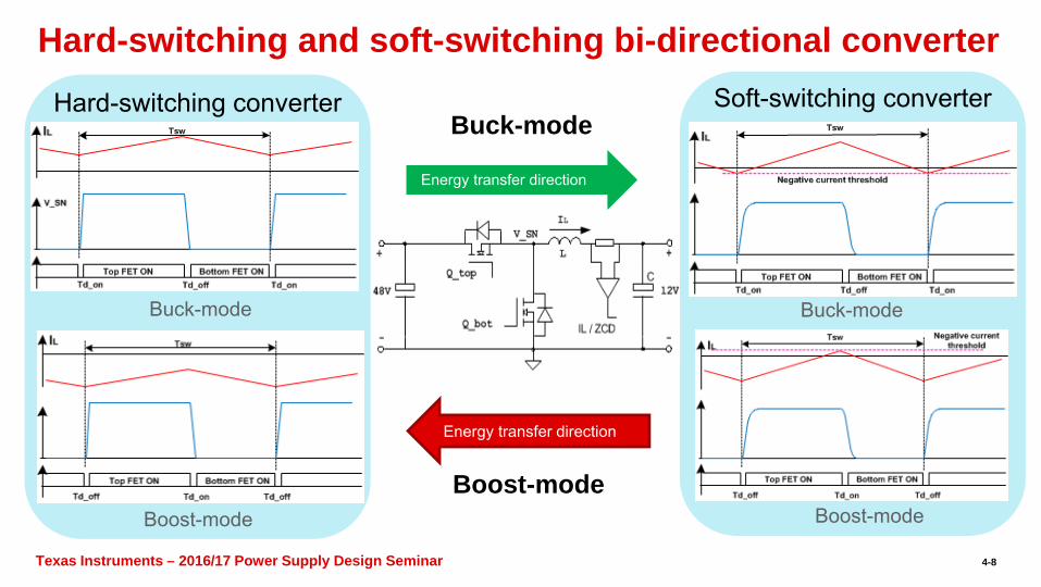
Hard-switching and soft-switching bi-directional converter
Buck-mode
Boost-mode
Buck-mode
Boost-mode
Energy transfer direction
Energy transfer direction
Soft-switching converterHard-switching converter
Buck-mode
Boost-mode
4-8
Texas Instruments – 2016/17 Power Supply Design SeminarTexas Instruments – 2016/17 Power Supply Design Seminar
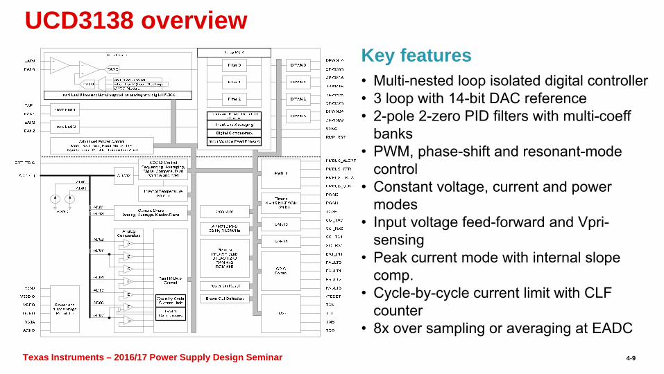
UCD3138 overviewKey features• Multi-nested loop isolated digital controller• 3 loop with 14-bit DAC reference• 2-pole 2-zero PID filters with multi-coeff
banks• PWM, phase-shift and resonant-mode
control • Constant voltage, current and power
modes• Input voltage feed-forward and Vpri-
sensing• Peak current mode with internal slope
comp.• Cycle-by-cycle current limit with CLF
counter• 8x over sampling or averaging at EADC
4-9
Texas Instruments – 2016/17 Power Supply Design SeminarTexas Instruments – 2016/17 Power Supply Design Seminar
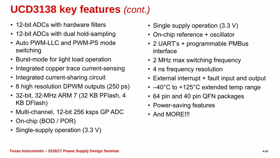
UCD3138 key features (cont.)• 12-bit ADCs with hardware filters• 12-bit ADCs with dual hold-sampling • Auto PWM-LLC and PWM-PS mode
switching• Burst-mode for light load operation• Integrated copper trace current-sensing• Integrated current-sharing circuit• 8 high resolution DPWM outputs (250 ps) • 32-bit, 32-MHz ARM 7 (32 KB PFlash, 4
KB DFlash)• Multi-channel, 12-bit 256 ksps GP ADC• On-chip (BOD / POR)• Single-supply operation (3.3 V)
• Single supply operation (3.3 V)• On-chip reference + oscillator• 2 UART’s + programmable PMBus
interface• 2 MHz max switching frequency• 4 ns frequency resolution• External interrupt + fault input and output• –40°C to +125°C extended temp range• 64 pin and 40 pin QFN packages• Power-saving features• And MORE!!!
4-10
Texas Instruments – 2016/17 Power Supply Design SeminarTexas Instruments – 2016/17 Power Supply Design Seminar
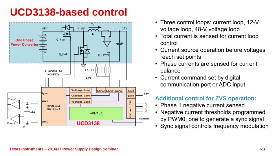
UCD3138-based control• Three control loops: current loop, 12-V
voltage loop, 48-V voltage loop• Total current is sensed for current loop
control• Current source operation before voltages
reach set points• Phase currents are sensed for current
balance• Current command set by digital
communication port or ADC input
Additional control for ZVS operation:• Phase 1 negative current sensed• Negative current thresholds programmed
by PWM0, one to generate a sync signal• Sync signal controls frequency modulation
4-11
Texas Instruments – 2016/17 Power Supply Design SeminarTexas Instruments – 2016/17 Power Supply Design Seminar
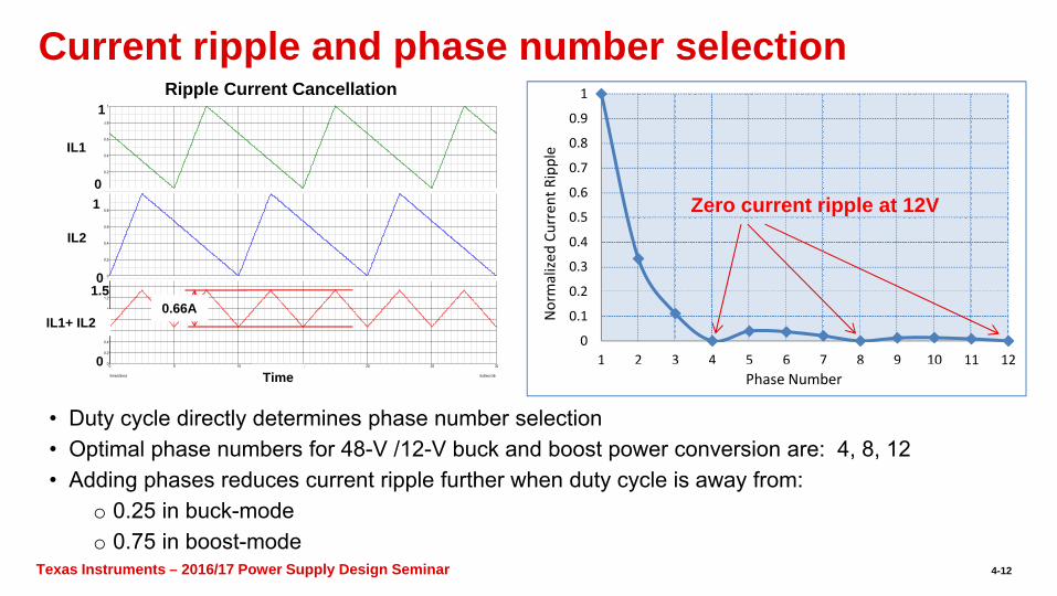
Current ripple and phase number selection
• Duty cycle directly determines phase number selection• Optimal phase numbers for 48-V /12-V buck and boost power conversion are: 4, 8, 12• Adding phases reduces current ripple further when duty cycle is away from:
o 0.25 in buck-modeo 0.75 in boost-mode
IL2
/ V
0.2
0.4
0.6
0.8
1
IL1
/ V
0
0.2
0.4
0.6
0.8
time/uSecs 5uSecs/div
0 5 10 15 20 25 30
IL_T
otal
/ V
0
0.2
0.4
0.6
0.8
1
1.2
1.4
Time
IL1
IL2
IL1+ IL2
0
1
0
1
0
1.50.66A
Ripple Current Cancellation
0
0.1
0.2
0.3
0.4
0.5
0.6
0.7
0.8
0.9
1
1 2 3 4 5 6 7 8 9 10 11 12Normalized Inductor Current Ripple vs Phase NumberPhase Number
Normalize
d Cu
rren
t Ripple
Zero current ripple at 12V
4-12
Texas Instruments – 2016/17 Power Supply Design SeminarTexas Instruments – 2016/17 Power Supply Design Seminar
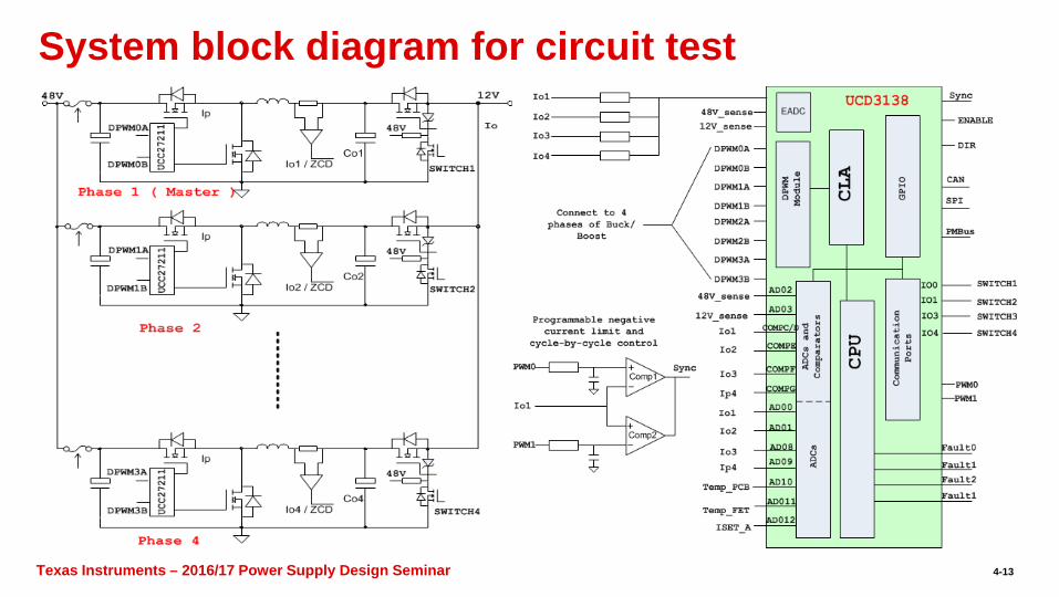
System block diagram for circuit test
4-13
Texas Instruments – 2016/17 Power Supply Design SeminarTexas Instruments – 2016/17 Power Supply Design Seminar
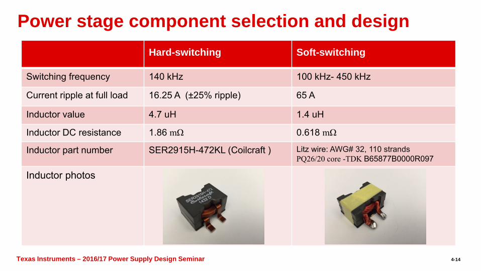
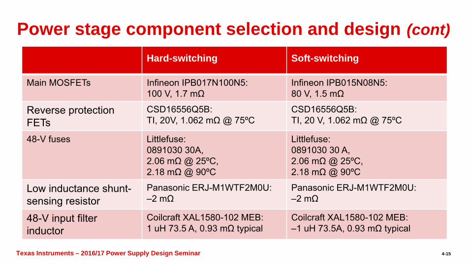
Power stage component selection and designHard-switching Soft-switching
Switching frequency 140 kHz 100 kHz- 450 kHz
Current ripple at full load 16.25 A (±25% ripple) 65 A
Inductor value 4.7 uH 1.4 uH
Inductor DC resistance 1.86 mΩ 0.618 mΩ
Inductor part number SER2915H-472KL (Coilcraft ) Litz wire: AWG# 32, 110 strands PQ26/20 core -TDK B65877B0000R097
Inductor photos
4-14
Texas Instruments – 2016/17 Power Supply Design SeminarTexas Instruments – 2016/17 Power Supply Design Seminar
Power stage component selection and design (cont)Hard-switching Soft-switching
Main MOSFETs Infineon IPB017N100N5:100 V, 1.7 mΩ
Infineon IPB015N08N5:80 V, 1.5 mΩ
Reverse protection FETs
CSD16556Q5B:TI, 20V, 1.062 mΩ @ 75ºC
CSD16556Q5B:TI, 20 V, 1.062 mΩ @ 75ºC
48-V fuses Littlefuse: 0891030 30A, 2.06 mΩ @ 25ºC,2.18 mΩ @ 90ºC
Littlefuse: 0891030 30 A, 2.06 mΩ @ 25ºC,2.18 mΩ @ 90ºC
Low inductance shunt-sensing resistor
Panasonic ERJ-M1WTF2M0U: –2 mΩ
Panasonic ERJ-M1WTF2M0U: –2 mΩ
48-V input filter inductor
Coilcraft XAL1580-102 MEB:1 uH 73.5 A, 0.93 mΩ typical
Coilcraft XAL1580-102 MEB: –1 uH 73.5A, 0.93 mΩ typical
4-15
Texas Instruments – 2016/17 Power Supply Design SeminarTexas Instruments – 2016/17 Power Supply Design Seminar
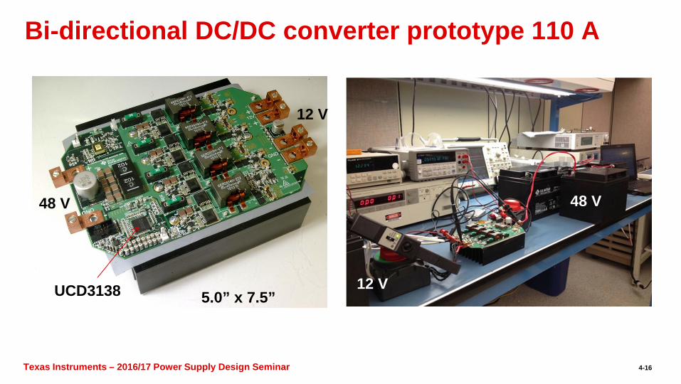
Bi-directional DC/DC converter prototype 110 A
5.0” x 7.5”
48 V
12 VUCD3138
48 V
12 V
4-16
Texas Instruments – 2016/17 Power Supply Design SeminarTexas Instruments – 2016/17 Power Supply Design Seminar
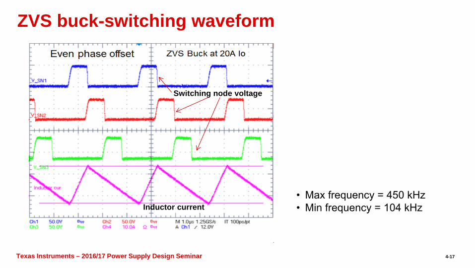
ZVS buck-switching waveform
ZVS Buck at 20A Io
• Max frequency = 450 kHz• Min frequency = 104 kHz
Switching node voltage
Inductor current
4-17
Texas Instruments – 2016/17 Power Supply Design SeminarTexas Instruments – 2016/17 Power Supply Design Seminar
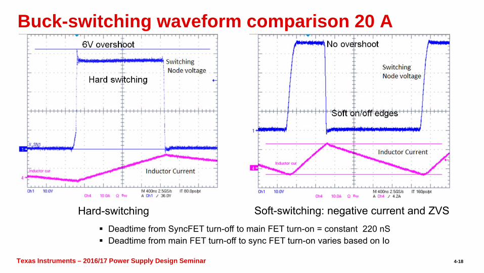
Buck-switching waveform comparison 20 A
Soft-switching: negative current and ZVS Deadtime from SyncFET turn-off to main FET turn-on = constant 220 nS Deadtime from main FET turn-off to sync FET turn-on varies based on Io
Hard-switching
Soft on/off edges
6V overshoot
Hard switching
No overshoot
4-18
Texas Instruments – 2016/17 Power Supply Design SeminarTexas Instruments – 2016/17 Power Supply Design Seminar
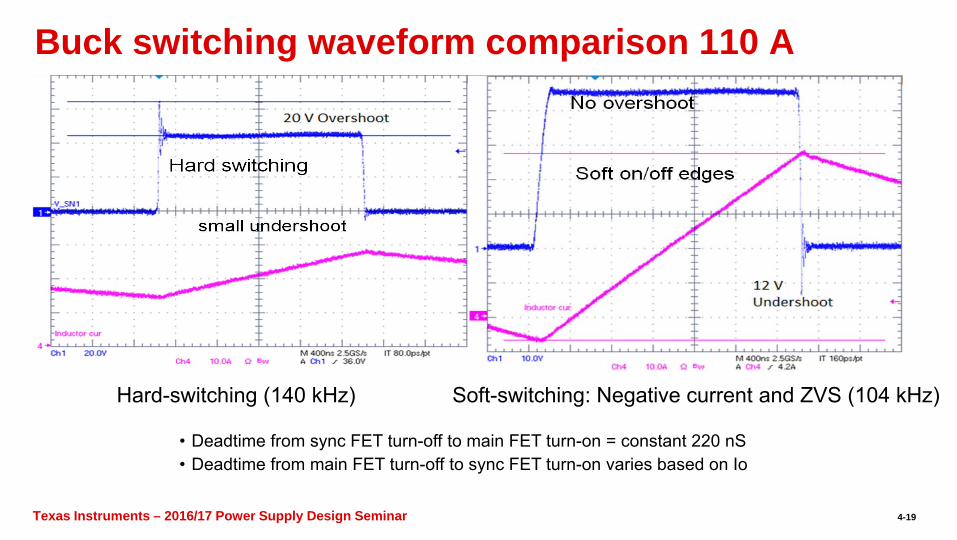
Buck switching waveform comparison 110 A
Soft-switching: Negative current and ZVS (104 kHz)
• Deadtime from sync FET turn-off to main FET turn-on = constant 220 nS• Deadtime from main FET turn-off to sync FET turn-on varies based on Io
Hard-switching (140 kHz)
20V overshoot
Soft on/off edgesHard switching
No overshoot
small undershoot
4-19
Texas Instruments – 2016/17 Power Supply Design SeminarTexas Instruments – 2016/17 Power Supply Design Seminar
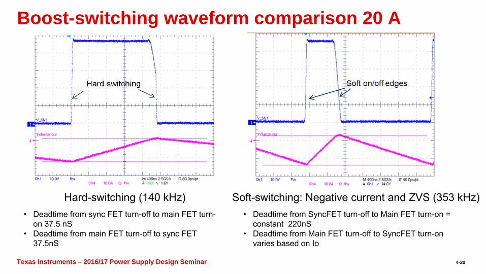
Boost-switching waveform comparison 20 A
• Deadtime from SyncFET turn-off to Main FET turn-on = constant 220nS
• Deadtime from Main FET turn-off to SyncFET turn-on varies based on Io
Soft-switching: Negative current and ZVS (353 kHz)Hard-switching (140 kHz) • Deadtime from sync FET turn-off to main FET turn-
on 37.5 nS• Deadtime from main FET turn-off to sync FET
37.5nS
Soft on/off edgesHard switching
4-20
Texas Instruments – 2016/17 Power Supply Design SeminarTexas Instruments – 2016/17 Power Supply Design Seminar
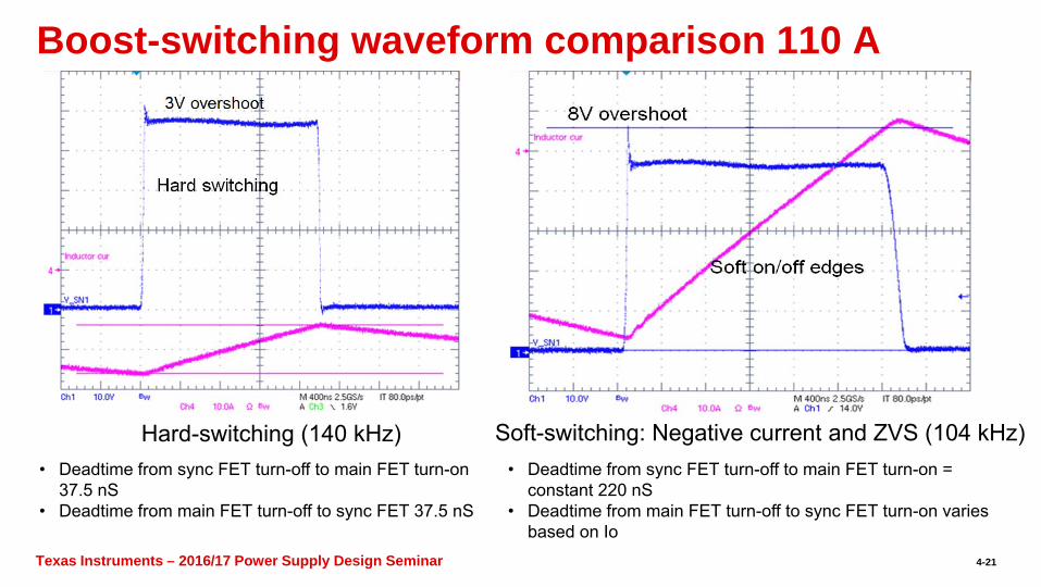
Boost-switching waveform comparison 110 A
• Deadtime from sync FET turn-off to main FET turn-on = constant 220 nS
• Deadtime from main FET turn-off to sync FET turn-on varies based on Io
Soft-switching: Negative current and ZVS (104 kHz)Hard-switching (140 kHz)• Deadtime from sync FET turn-off to main FET turn-on
37.5 nS• Deadtime from main FET turn-off to sync FET 37.5 nS
3V overshoot
Soft on/off edges
Hard switching
8V overshoot
4-21
Texas Instruments – 2016/17 Power Supply Design SeminarTexas Instruments – 2016/17 Power Supply Design Seminar
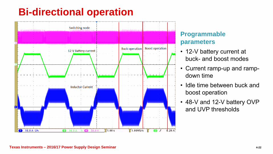
Bi-directional operation
Ibat
IL
VSN
Programmable parameters• 12-V battery current at
buck- and boost modes• Current ramp-up and ramp-
down time• Idle time between buck and
boost operation• 48-V and 12-V battery OVP
and UVP thresholds
4-22
Texas Instruments – 2016/17 Power Supply Design SeminarTexas Instruments – 2016/17 Power Supply Design Seminar
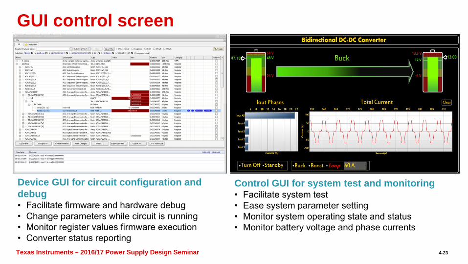
GUI control screen
Device GUI for circuit configuration and debug• Facilitate firmware and hardware debug• Change parameters while circuit is running• Monitor register values firmware execution• Converter status reporting
Control GUI for system test and monitoring• Facilitate system test• Ease system parameter setting• Monitor system operating state and status• Monitor battery voltage and phase currents
4-23
Texas Instruments – 2016/17 Power Supply Design SeminarTexas Instruments – 2016/17 Power Supply Design Seminar
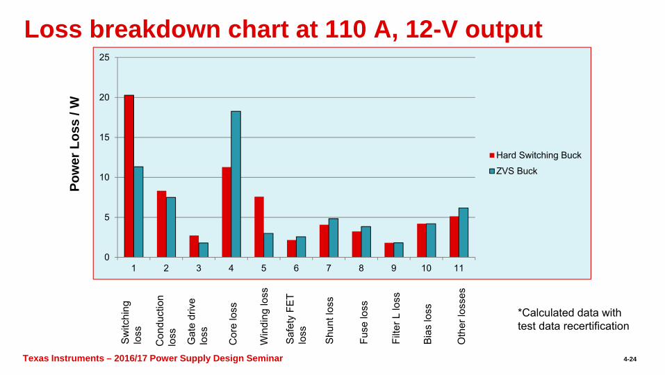
Loss breakdown chart at 110 A, 12-V output
0
5
10
15
20
25
1 2 3 4 5 6 7 8 9 10 11
Hard Switching Buck
ZVS Buck
Sw
itchi
ng
loss
Con
duct
ion
loss Gat
e dr
ive
loss
Cor
e lo
ss
Win
ding
loss
Saf
ety
FET
loss
Shu
nt lo
ss
Fuse
loss
Filte
r L lo
ss
Bia
s lo
ss
Oth
er lo
sses
Pow
er L
oss
/ W
*Calculated data with test data recertification
4-24
Texas Instruments – 2016/17 Power Supply Design SeminarTexas Instruments – 2016/17 Power Supply Design Seminar
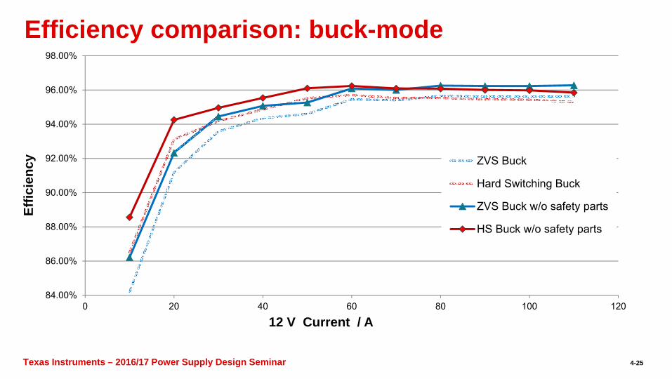
Efficiency comparison: buck-mode
84.00%
86.00%
88.00%
90.00%
92.00%
94.00%
96.00%
98.00%
0 20 40 60 80 100 120
ZVS Buck
Hard Switching Buck
ZVS Buck w/o safety parts
HS Buck w/o safety parts
Effic
ienc
y
12 V Current / A
4-25
Texas Instruments – 2016/17 Power Supply Design SeminarTexas Instruments – 2016/17 Power Supply Design Seminar
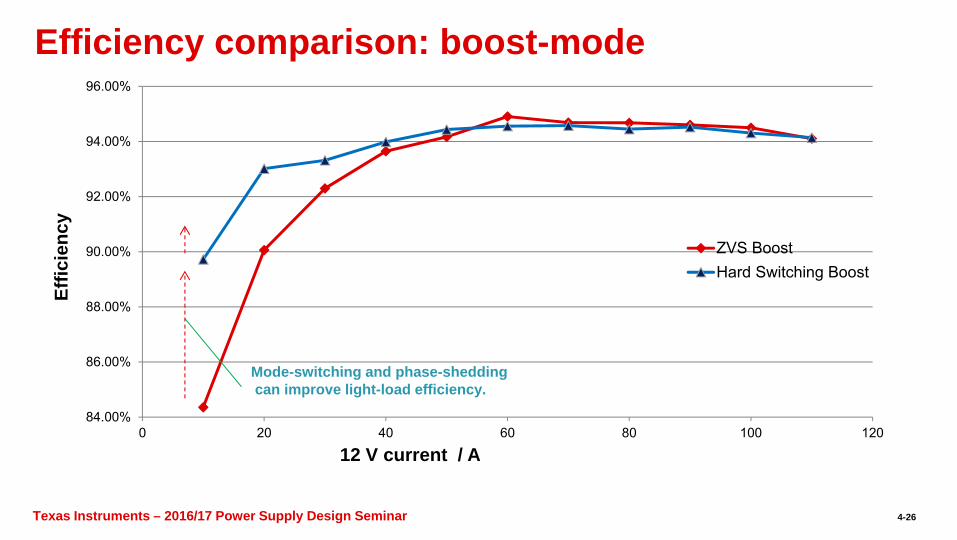
Efficiency comparison: boost-mode
84.00%
86.00%
88.00%
90.00%
92.00%
94.00%
96.00%
0 20 40 60 80 100 120
ZVS BoostHard Switching Boost
Mode-switching and phase-sheddingcan improve light-load efficiency.
Effic
ienc
y
12 V current / A
4-26
Texas Instruments – 2016/17 Power Supply Design SeminarTexas Instruments – 2016/17 Power Supply Design Seminar
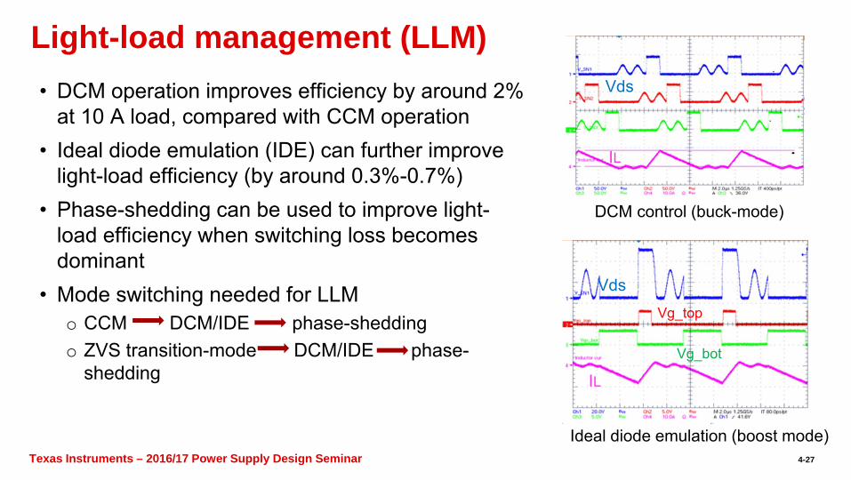
Light-load management (LLM)• DCM operation improves efficiency by around 2%
at 10 A load, compared with CCM operation• Ideal diode emulation (IDE) can further improve
light-load efficiency (by around 0.3%-0.7%)• Phase-shedding can be used to improve light-
load efficiency when switching loss becomes dominant
• Mode switching needed for LLMo CCM DCM/IDE phase-sheddingo ZVS transition-mode DCM/IDE phase-
shedding
DCM control (buck-mode)
Ideal diode emulation (boost mode)
Vds
IL
Vds
IL
Vg_top
Vg_bot
4-27
Texas Instruments – 2016/17 Power Supply Design SeminarTexas Instruments – 2016/17 Power Supply Design Seminar
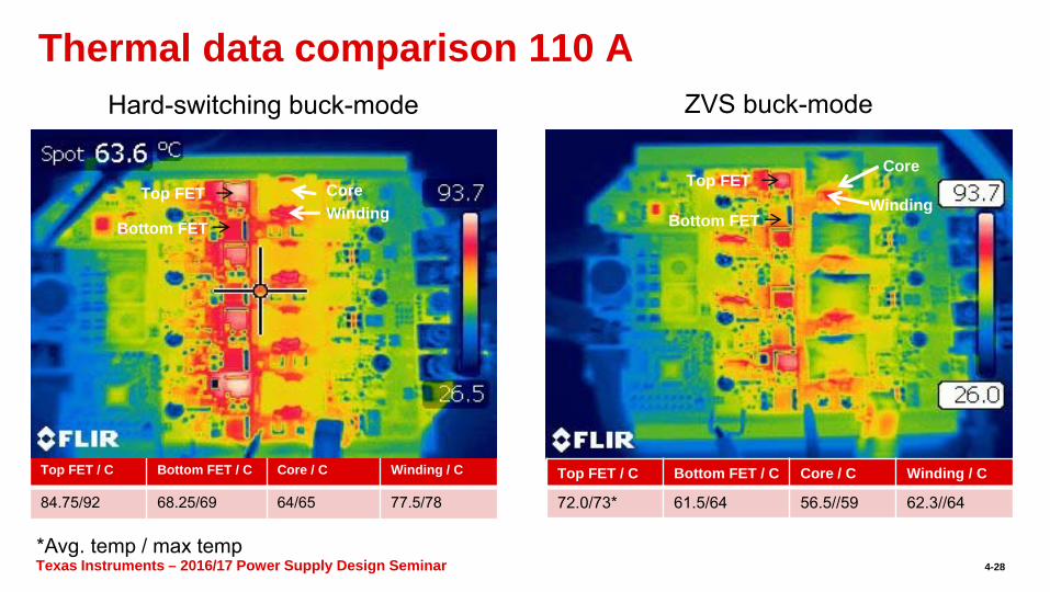
Thermal data comparison 110 AZVS buck-modeHard-switching buck-mode
Top FET / C Bottom FET / C Core / C Winding / C
72.0/73* 61.5/64 56.5//59 62.3//64
Top FET / C Bottom FET / C Core / C Winding / C
84.75/92 68.25/69 64/65 77.5/78
*Avg. temp / max temp
Top FET
Bottom FET
Top FET
Bottom FET
CoreWinding
Core
Winding
4-28
Texas Instruments – 2016/17 Power Supply Design SeminarTexas Instruments – 2016/17 Power Supply Design Seminar
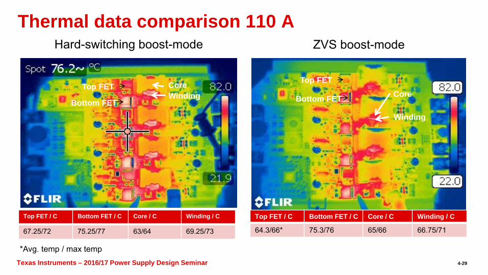
Thermal data comparison 110 AZVS boost-modeHard-switching boost-mode
Top FET / C Bottom FET / C Core / C Winding / C
64.3/66* 75.3/76 65/66 66.75/71
Top FET / C Bottom FET / C Core / C Winding / C
67.25/72 75.25/77 63/64 69.25/73
Top FET
Bottom FET
Top FET
Bottom FETCoreWinding
Winding
Core
*Avg. temp / max temp4-29
Texas Instruments – 2016/17 Power Supply Design SeminarTexas Instruments – 2016/17 Power Supply Design Seminar
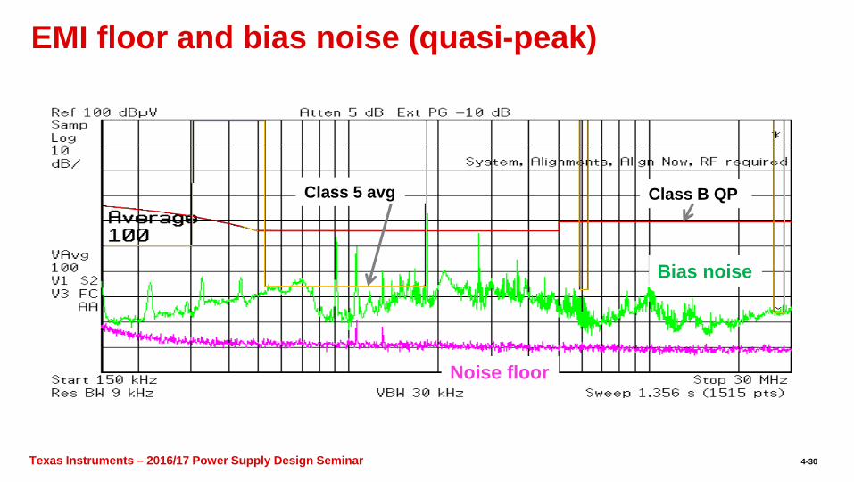
EMI floor and bias noise (quasi-peak)
Noise floor
Bias noise
Class B QP Class 5 avg
4-30
Texas Instruments – 2016/17 Power Supply Design SeminarTexas Instruments – 2016/17 Power Supply Design Seminar
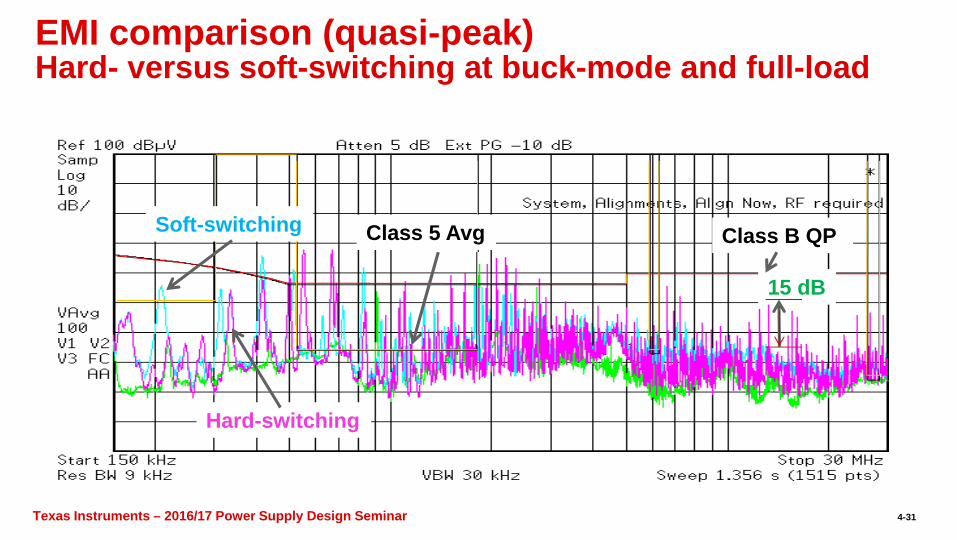
EMI comparison (quasi-peak)Hard- versus soft-switching at buck-mode and full-load
15 dB
Class B QP Class 5 AvgSoft-switching
Hard-switching
4-31
Texas Instruments – 2016/17 Power Supply Design SeminarTexas Instruments – 2016/17 Power Supply Design Seminar
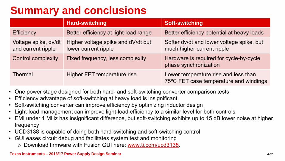
Summary and conclusionsHard-switching Soft-switching
Efficiency Better efficiency at light-load range Better efficiency potential at heavy loads
Voltage spike, dv/dtand current ripple
Higher voltage spike and dV/dt but lower current ripple
Softer dv/dt and lower voltage spike, but much higher current ripple
Control complexity Fixed frequency, less complexity Hardware is required for cycle-by-cycle phase synchronization
Thermal Higher FET temperature rise Lower temperature rise and less than 75ºC FET case temperature and windings
• One power stage designed for both hard- and soft-switching converter comparison tests• Efficiency advantage of soft-switching at heavy load is insignificant• Soft-switching converter can improve efficiency by optimizing inductor design• Light-load management can improve light-load efficiency to a similar level for both controls• EMI under 1 MHz has insignificant difference, but soft-switching exhibits up to 15 dB lower noise at higher
frequency • UCD3138 is capable of doing both hard-switching and soft-switching control • GUI eases circuit debug and facilitates system test and monitoring
o Download firmware with Fusion GUI here: www.ti.com/ucd3138.4-32
The platform bar and E2E are trademarks of Texas Instruments. All other trademarks are the property of their respective owners. SLUP343
TI Worldwide Technical Support
InternetTI Semiconductor Product Information Center Home Pagesupport.ti.comTI E2E™ Community Home Pagee2e.ti.com
Product Information CentersPhone +1(512) 434-1560
Phone
Americas Brazil Mexico Phone
0800-891-2616
0800-670-7544
Fax Internet/Email
+1(972) 927-6377support.ti.com/sc/pic/americas.htm
Europe, Middle East, and AfricaPhone
European Free Call 00800-ASK-TEXAS (00800 275 83927)
International +49 (0) 8161 80 2121
Russian Support +7 (4) 95 98 10 701
Note: The European Free Call (Toll Free) number is not active in all countries. If you have technical difficulty calling the free call number, please use the international number above.
Fax Internet Direct Email
+(49) (0) 8161 80 2045www.ti.com/[email protected]
JapanPhone Domestic 0120-92-3326Fax International
Domestic +81-3-3344-5317
0120-81-0036Internet/Email International
Domestic support.ti.com/sc/pic/japan.htm
www.tij.co.jp/pic
AsiaPhone
+91-80-41381665International Domestic Toll-Free Number
Note: Toll-free numbers do not support mobile and IP phones.
1-800-999-084Australia China Hong Kong India Indonesia Korea Malaysia New Zealand Philippines Singapore
Taiwan Thailand
800-820-8682 800-96-5941000-800-100-8888 001-803-8861-1006 080-551-28041-800-80-3973 0800-446-9341-800-765-7404 800-886-1028 0800-006800001-800-886-0010
International Fax Email Internet
[email protected] or [email protected] support.ti.com/sc/pic/asia.htm
B021014
Important Notice: The products and services of Texas Instruments Incorporated and its subsidiaries described herein are sold subject to TI’s standard terms and conditions of sale. Customers are advised to obtain the most current and complete information about TI products and services before placing orders. TI assumes no liability for applications assistance, customer’s applications or product designs, software performance, or infringement of patents. The publication of information regarding any other company’s products or services does not constitute TI’s approval, warranty or endorsement thereof.
IMPORTANT NOTICE
Texas Instruments Incorporated and its subsidiaries (TI) reserve the right to make corrections, enhancements, improvements and otherchanges to its semiconductor products and services per JESD46, latest issue, and to discontinue any product or service per JESD48, latestissue. Buyers should obtain the latest relevant information before placing orders and should verify that such information is current andcomplete. All semiconductor products (also referred to herein as “components”) are sold subject to TI’s terms and conditions of salesupplied at the time of order acknowledgment.TI warrants performance of its components to the specifications applicable at the time of sale, in accordance with the warranty in TI’s termsand conditions of sale of semiconductor products. Testing and other quality control techniques are used to the extent TI deems necessaryto support this warranty. Except where mandated by applicable law, testing of all parameters of each component is not necessarilyperformed.TI assumes no liability for applications assistance or the design of Buyers’ products. Buyers are responsible for their products andapplications using TI components. To minimize the risks associated with Buyers’ products and applications, Buyers should provideadequate design and operating safeguards.TI does not warrant or represent that any license, either express or implied, is granted under any patent right, copyright, mask work right, orother intellectual property right relating to any combination, machine, or process in which TI components or services are used. Informationpublished by TI regarding third-party products or services does not constitute a license to use such products or services or a warranty orendorsement thereof. Use of such information may require a license from a third party under the patents or other intellectual property of thethird party, or a license from TI under the patents or other intellectual property of TI.Reproduction of significant portions of TI information in TI data books or data sheets is permissible only if reproduction is without alterationand is accompanied by all associated warranties, conditions, limitations, and notices. TI is not responsible or liable for such altereddocumentation. Information of third parties may be subject to additional restrictions.Resale of TI components or services with statements different from or beyond the parameters stated by TI for that component or servicevoids all express and any implied warranties for the associated TI component or service and is an unfair and deceptive business practice.TI is not responsible or liable for any such statements.Buyer acknowledges and agrees that it is solely responsible for compliance with all legal, regulatory and safety-related requirementsconcerning its products, and any use of TI components in its applications, notwithstanding any applications-related information or supportthat may be provided by TI. Buyer represents and agrees that it has all the necessary expertise to create and implement safeguards whichanticipate dangerous consequences of failures, monitor failures and their consequences, lessen the likelihood of failures that might causeharm and take appropriate remedial actions. Buyer will fully indemnify TI and its representatives against any damages arising out of the useof any TI components in safety-critical applications.In some cases, TI components may be promoted specifically to facilitate safety-related applications. With such components, TI’s goal is tohelp enable customers to design and create their own end-product solutions that meet applicable functional safety standards andrequirements. Nonetheless, such components are subject to these terms.No TI components are authorized for use in FDA Class III (or similar life-critical medical equipment) unless authorized officers of the partieshave executed a special agreement specifically governing such use.Only those TI components which TI has specifically designated as military grade or “enhanced plastic” are designed and intended for use inmilitary/aerospace applications or environments. Buyer acknowledges and agrees that any military or aerospace use of TI componentswhich have not been so designated is solely at the Buyer's risk, and that Buyer is solely responsible for compliance with all legal andregulatory requirements in connection with such use.TI has specifically designated certain components as meeting ISO/TS16949 requirements, mainly for automotive use. In any case of use ofnon-designated products, TI will not be responsible for any failure to meet ISO/TS16949.
Products ApplicationsAudio www.ti.com/audio Automotive and Transportation www.ti.com/automotiveAmplifiers amplifier.ti.com Communications and Telecom www.ti.com/communicationsData Converters dataconverter.ti.com Computers and Peripherals www.ti.com/computersDLP® Products www.dlp.com Consumer Electronics www.ti.com/consumer-appsDSP dsp.ti.com Energy and Lighting www.ti.com/energyClocks and Timers www.ti.com/clocks Industrial www.ti.com/industrialInterface interface.ti.com Medical www.ti.com/medicalLogic logic.ti.com Security www.ti.com/securityPower Mgmt power.ti.com Space, Avionics and Defense www.ti.com/space-avionics-defenseMicrocontrollers microcontroller.ti.com Video and Imaging www.ti.com/videoRFID www.ti-rfid.comOMAP Applications Processors www.ti.com/omap TI E2E Community e2e.ti.comWireless Connectivity www.ti.com/wirelessconnectivity
Mailing Address: Texas Instruments, Post Office Box 655303, Dallas, Texas 75265Copyright © 2016, Texas Instruments Incorporated