Embed Size (px)
Citation preview
HAL Id: hal-02395111https://hal.archives-ouvertes.fr/hal-02395111
Submitted on 13 Feb 2020
HAL is a multi-disciplinary open accessarchive for the deposit and dissemination of sci-entific research documents, whether they are pub-lished or not. The documents may come fromteaching and research institutions in France orabroad, or from public or private research centers.
L’archive ouverte pluridisciplinaire HAL, estdestinée au dépôt et à la diffusion de documentsscientifiques de niveau recherche, publiés ou non,émanant des établissements d’enseignement et derecherche français ou étrangers, des laboratoirespublics ou privés.
A Bidirectional Communicating Power Supply circuitfor Smart Gate Driver boards
Julien Weckbrodt, Nicolas Ginot, Christophe Batard, Thanh Long Le,Stéphane Azzopardi
To cite this version:Julien Weckbrodt, Nicolas Ginot, Christophe Batard, Thanh Long Le, Stéphane Azzopardi. A Bidi-rectional Communicating Power Supply circuit for Smart Gate Driver boards. IEEE Transactionson Power Electronics, Institute of Electrical and Electronics Engineers, 2020, 35 (8), pp.8540-8549.10.1109/TPEL.2019.2960632. hal-02395111
This article has been accepted for publication in a future issue of this journal, but has not been fully edited. Content may change prior to final publication. Citation information: DOI 10.1109/TPEL.2019.2960632, IEEETransactions on Power Electronics
IEEE POWER ELECTRONICS REGULAR PAPER/LETTER/CORRESPONDENCE
A Bidirectional Communicating Power Supply circuit
for Smart Gate Driver boardsJulien Weckbrodt, Nicolas Ginot, Christophe Batard, Thanh Long Le, Stéphane Azzopardi
Abstract- In power circuits, the gate drivers are required to
provide an optimal and safe switching of power semiconductor
devices. Nowadays, the gate driver boards include more and more
features such as short-circuit detection, soft-shutdown,
temperature sensing, on-state voltage monitoring… Research
works are in progress on the integration of on-line monitoring
features for a predictive maintenance. The instrumentation of the
gate drive system supposes the integration of a communication
system to transmit the monitoring data. In high power designs, a
galvanic isolation is mandatory on the gate driver board. The
parasitic capacitance seen on the isolation barrier is critical in
these designs as it can lead to the circulation of common mode
currents during the switching. Adding extra optocouplers or
transformers on the isolation barrier is therefore risky due to
ElectroMagnetic Interference (EMI) constraints. In this paper, a
new bidirectional data transmission method is proposed for gate
drivers used for driving 1.2kV SiC power MOSFETs. The
proposed method enables the energy transmission and a
bidirectional data exchange on a single power supply transformer.
Experimental results are provided demonstrating 1Mb/s for TxD
and 16kb/s for RxD. The targeted application is the health
monitoring of SiC power MOSFETs using the gate driver board.
Index Terms- Communication channel, driver circuits, electrical
isolation, power system monitoring, isolated power supply, SiC
MOSFET.
I. INTRODUCTION
Silicon Carbide (SiC) power transistors such as SiC power
Metal Oxide Semiconductor Field Effect Transistor
(MOSFETs) are more and more used in power converters.
These components are excellent candidates to replace the
Silicon-based devices in power circuits. The interesting
properties of SiC power components enables operation at
higher frequency and higher temperature. Indeed, compared to
Silicon devices, the fast switching of SiC MOSFET reduces
considerably the switching losses. Their performances in high
temperature conditions also enable a higher power density for
energy converters. Many research works on robustness have
been carried out since the emergence of SiC-based power
transistors. Recent studies have pointed out ageing indicators
which could be used for health monitoring purposes such as the
evolution of the gate leakage current [1-5] or the on-state
resistance [1-4], [6]. The on-line monitoring of these electrical
parameters requires measurement circuits and a data exchange
on the gate drive system. Implementing such methods could
help to prevent damages by detecting ageing before failures.
The targeted application is the predictive maintenance for high
reliability power circuits in aeronautical environments.
In power electronics designs, the gate driver provides an
optimal command of the power semiconductor device using an
electrically isolated circuit. For safety reasons, this electric
isolation is mandatory in high voltage circuits. As a result, the
driver board is divided in two parts: the primary circuit
connected to the control unit and the secondary circuit close to
the power semiconductor device. The ground potential on the
secondary circuit is fixed by the source/emitter voltage of the
power component (Kelvin connection). The galvanic isolation
represents a major constraint for the integration of intelligent
circuits on the gate driver board. The new SiC power
semiconductor devices can reduce the energy losses during the
switching as it can switch faster than Silicon ones. As a result,
electromagnetic interferences are even more restrictive in SiC
gate driver designs due to high dv/dt during the turn-on and the
turn-off.
Although optocouplers or optical fibers can be used to
transmit switching orders, transformers are always used in gate
drive topologies, at least to provide supply voltage to the
secondary circuit. In conventional gate driver boards, the only
information transmitted across the isolation barrier is the
switching orders (PWM) and an error signal, in the event of a
fault detection [7-10]. Nowadays, new “smart gate drivers”
enable data exchange by the addition of transformers dedicated
to communication across the electrical isolation [11-14].
Adding extra transformers across the isolation is quite
cumbersome and it can lead to the circulation of parasitic
common mode currents as they introduce extra capacitances
between the primary and the secondary circuit. The common
mode current is a well-known issue in gate drive topologies.
Several research works proposed optimizations to reduce this
parasitic current [10-11, 16-19]. In [16], a supply circuit is
studied to reduce the coupling capacitance using a coupled filter
inductor on the power circuit. Cascaded gate driver supply
architectures were analyzed in [18, 19]. Architectures were
proposed in which the power supply circuits are pooled in order
to reduce the resulting common mode current under very high
Manuscript received July 24, 2019…
…
… …
…
… …
…
…
Accep
ted M
anus
cript
This article has been accepted for publication in a future issue of this journal, but has not been fully edited. Content may change prior to final publication. Citation information: DOI 10.1109/TPEL.2019.2960632, IEEETransactions on Power Electronics
IEEE POWER ELECTRONICS REGULAR PAPER/LETTER/CORRESPONDENCE
dv/dt. This solution treats the problem of EMI interference at
the converter level considering several power transistors. As
explained in [16-19], the electromagnetic perturbations are due
to the high dv/dt applied between the primary and the secondary
ground potentials during the switching of the power device.
The interest of communication on power circuitry is not new
and many works have been carried out in the field of Power-
Line Communication (PLC) [20-22]. However, such methods
of communication are not applicable for highly constrained
isolated designs confronted to high dv/dt due to the proximity
of the switching cells. In this context, the addition of
communication features within the gate driver board with no
significant impact on the common mode current represents a
real challenge. Yang et al. [23] reported an isolated full-bridge
DC-DC converter with a 1MHz bidirectional communication
channel. Unfortunately, no test was performed to check the
dv/dt immunity since the operating principle and the targeted
application are different from the presented method.
In this paper, power supply structures based on the DC-DC
Push-Pull operating principle are described in the following
section. A method for DATA exchange using the power supply
circuit is proposed in section III. The operating principle and
simulations using SPICE models are detailed. Experimental
setup and waveforms are then provided in order to check the
feasibility of the proposed solution. Finally, the designed circuit
is confronted with high dv/dt to test the communication system
in a severe environment. Experimental waveforms
corresponding to a 400V/200A switching in a DC-DC Buck
converter are also provided.
II. CONVENTIONAL POWER SUPPLY TOPOLOGIES USED IN GATE
DRIVER BOARDS
In the case of gate drivers used to drive Insulated Gate
Bipolar Transistors (IGBTs), a symmetrical supply voltage is
often required (+15V/-15V). Since the new SiC power
MOSFETs generally require a +20V/-5V gate-source voltage
for optimal switching, a 25V power supply voltage is required
for driving such components. There are two main solutions for
providing the supply voltage: a bootstrap circuit or an isolated
DC/DC converter. Power supply circuit based on bootstrap
circuit is generally chosen in low-cost or low-voltage
(a)
(b)
(c)
(d)
Fig. 2. Open loop Push-Pull converters with fixed duty cycle – State of the art
on the power supply circuits in commercially available gate driver boards: (a) Infineon 2ED300C17; (b) Semikron SkyperPro32; (c) Cree
PT62SCMD12; (d) Power Integration 2SC0650.
VIN
0V
VH
-VL
0V
Reg.
VH
-VL
VIN
0V
VIN
VH
-VL
VSECVIN
0V
Re
f.
VH
-VL
TABLE I STATE OF THE ART ON GATE DRIVER BOARDS
Fig. Driver board
reference Supply circuit topology
Output
power /
channel
Total
parasitic
capacitance
2 (a)
2 (b)
2 (c)
2 (d)
-
4
2ED300C17
SkyperPro32
PT62SCMD12
2SC0650
CGD15HB62LP
This work
Open loop push-pull
Open loop push-pull
Open loop push-pull
Open loop push-pull
Flyback circuit
Open loop push-pull
4W
1.1W
3.5W
6W
6W
4W
18pF
12pF
-
28pF
17pF
13pF*
*8pF for the power supply and 5pF for the pulse transformer (@1MHz)
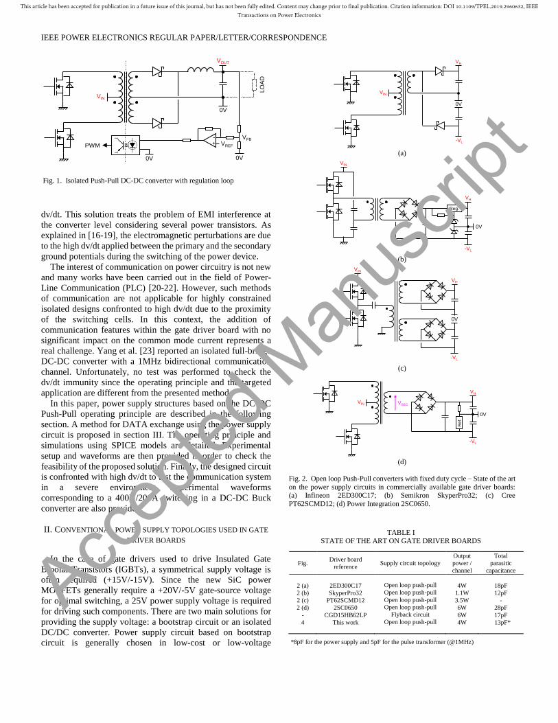
Fig. 1. Isolated Push-Pull DC-DC converter with regulation loop
VREF
VIN
0V
LO
AD
VOUT
0V
+-
0V
PWM
VFB
Accep
ted M
anus
cript
This article has been accepted for publication in a future issue of this journal, but has not been fully edited. Content may change prior to final publication. Citation information: DOI 10.1109/TPEL.2019.2960632, IEEETransactions on Power Electronics
IEEE POWER ELECTRONICS REGULAR PAPER/LETTER/CORRESPONDENCE
applications. In most cases, the isolated DC/DC converters are
preferred as an additional isolation is often required between
the high side (HS) transistor and low side (LS) transistor in a
half-bridge configuration. The isolated DC/DC converters used
in gate drivers are generally realized by a Push-Pull converter
or sometimes by a Flyback topology [7, 10, 24, 25]. Gate
drivers using an optical power transfer have also been studied
[26, 27]. Although these methods provide an optimal common-
mode rejection, the low efficiency of the photoelectric
transducers makes them inadequate for power modules
command (power consumption >1W). In this work, only the
Push-Pull DC/DC converters used as a power supply circuit in
driver boards will be considered.
The classical structure of Push-Pull converters is shown in
Fig. 1. The transistors at primary side are alternately switched
on and off, a short deadtime is observed in order to avoid short
circuits. The particularity of the Push-Pull converter is that the
current is drawn from the line during both halves of the
switching cycle. The stability of the output voltage is typically
ensured by a feedback using an optocoupler. However, as
explained before, the addition of elements over the isolation
barrier is problematic in gate drive boards. Consequently, open-
loop strucutres are always preferred for power supplies in the
gate drivers boards. The power consumption in gate driver
boards is relatively low (<10W) in comparison with the driven
power circuit (several kW). In addition, this low energy transfer
allows circuit simplifications as efficiency is not a critical
parameter in these designs. In Fig. 2, a state of the art of the
power supply circuits used in gate driver boards is presented.
These low-power DC/DC converters in open loop configuration
are derived from the Push-Pull converter topology. The main
characteristics of the driver boards mentioned in Fig. 2 are
described in Table I. In the rest of the paper, the circuit
presented in Fig. 2 (d) was chosen for demonstrating the
communication principle. In this circuit, a square signal with
fixed duty cycle is used to apply ±15V on the primary windings.
The secondary voltage VSEC periodically varies from +30V
to -30V. On the secondary side, the output voltage VOUT
corresponds to the double of the input voltage (transformer
turns ratio 2:1) reduced by the diodes voltage drop.
III. PROPOSED STRUCTURE FOR DATA EXCHANGE USING
THE ISOLATED POWER SUPPLY CIRCUIT
A. Operating principle
Since the addition of extra transformers or optocouplers
decreases the quality of the isolation barrier, the method
proposed in the present paper enables energy transfer and
DATA exchange on the same transformer. As explained in
Fig. 3, the isolated power supply circuit is used as a
communication channel between the primary circuit and the
secondary circuit. The operation can be divided in two steps:
phase A and phase B.
During the first period of time TA, the TxD signal is
transmitted using a Manchester code applied to the command
signal Cmd instead of the square signal described in section II.
The decoding of this signal can be realized at the secondary side
using a XOR logic gate. During this period, the energy and the
TxD signal are both transmitted through the transformer. A RC-
series snubber circuit was implemented in order to optimize the
switching of the transistors Q1 and Q3. Due to the Manchester
coding, the operating frequency of the proposed DC/DC
converter is not fixed. The frequency spectrum is spread
between 500kHz and 1MHz.
During the phase B, the energy transfer through the
transformer is stopped during a predetermined time (here
TB=11µs). At this moment, the transformer is demagnetized by
switching OFF the transistors Q1 and Q3 at the same time.
Oscillations may occur during the demagnetizing process.
These oscillations can be reduced by the addition of resistive
loads connected to the primary windings as shown in Fig. 5.
These loads are disabled during the phase A (signal En). They
Fig. 4. Proposed principle based on the topology presented in Fig. 2 (d)
0
1 10
Signal
VSEC
Manchester
coding
Proposed
signal
VSEC’
1 1
Power supply ON & TxD
T=1µs
A
1
1
10
0101111101000010
RxD
1
TB =11µs
B
1 001110
1
BA
TA + TB = 1ms
Fig. 3. Proposed strategy for online monitoring using a smart driver board
S
G
D
GATE DRIVER BOARDSiC POWER
MOSFET
PRIMARY
CIRCUIT
SECONDARY
CIRCUIT
Galvanic isolation
Orders
Error
Mode
TxD
RxD
PWM ORDERS
ERROR PULSE
TxD
RxD
State of
the art
COMMAND
UNIT
MONITORING
This
work
Power supply transformer
Accep
ted M
anus
cript
This article has been accepted for publication in a future issue of this journal, but has not been fully edited. Content may change prior to final publication. Citation information: DOI 10.1109/TPEL.2019.2960632, IEEETransactions on Power Electronics
IEEE POWER ELECTRONICS REGULAR PAPER/LETTER/CORRESPONDENCE
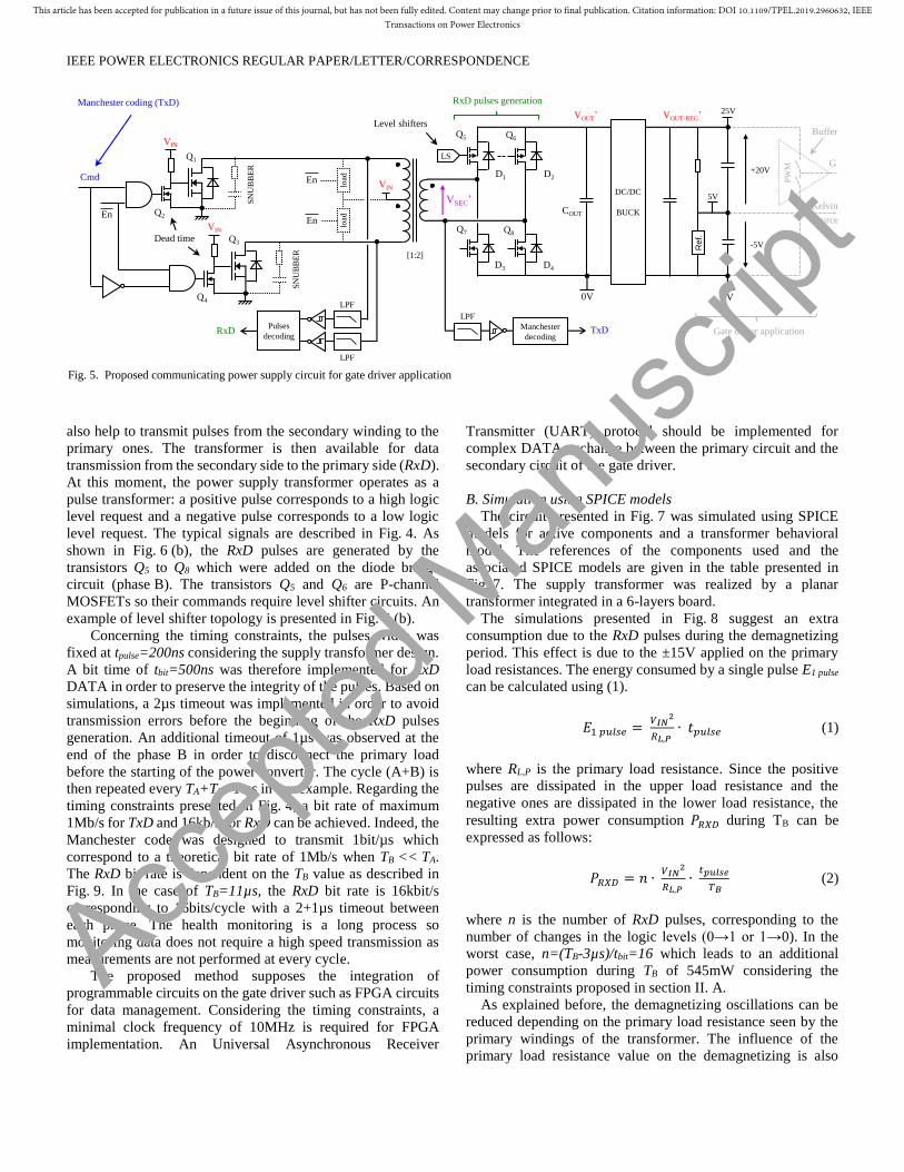
also help to transmit pulses from the secondary winding to the
primary ones. The transformer is then available for data
transmission from the secondary side to the primary side (RxD).
At this moment, the power supply transformer operates as a
pulse transformer: a positive pulse corresponds to a high logic
level request and a negative pulse corresponds to a low logic
level request. The typical signals are described in Fig. 4. As
shown in Fig. 6 (b), the RxD pulses are generated by the
transistors Q5 to Q8 which were added on the diode bridge
circuit (phase B). The transistors Q5 and Q6 are P-channel
MOSFETs so their commands require level shifter circuits. An
example of level shifter topology is presented in Fig. 6 (b). Concerning the timing constraints, the pulses width was
fixed at tpulse=200ns considering the supply transformer design.
A bit time of tbit=500ns was therefore implemented for RxD
DATA in order to preserve the integrity of the pulses. Based on
simulations, a 2µs timeout was implemented in order to avoid
transmission errors before the beginning of the RxD pulses
generation. An additional timeout of 1µs was observed at the
end of the phase B in order to disconnect the primary load
before the starting of the power converter. The cycle (A+B) is
then repeated every TA+TB=1ms in our example. Regarding the
timing constraints presented in Fig. 4, a bit rate of maximum
1Mb/s for TxD and 16kb/s for RxD can be achieved. Indeed, the
Manchester code was designed to transmit 1bit/µs which
correspond to a theoretical bit rate of 1Mb/s when TB << TA.
The RxD bit rate is dependent on the TB value as described in
Fig. 9. In the case of TB=11µs, the RxD bit rate is 16kbit/s
corresponding to 16bits/cycle with a 2+1µs timeout between
each phase. The health monitoring is a long process so
monitoring data does not require a high speed transmission as
measurements are not performed at every cycle.
The proposed method supposes the integration of
programmable circuits on the gate driver such as FPGA circuits
for data management. Considering the timing constraints, a
minimal clock frequency of 10MHz is required for FPGA
implementation. An Universal Asynchronous Receiver
Transmitter (UART) protocol should be implemented for
complex DATA exchange between the primary circuit and the
secondary circuit of the gate driver.
B. Simulation using SPICE models
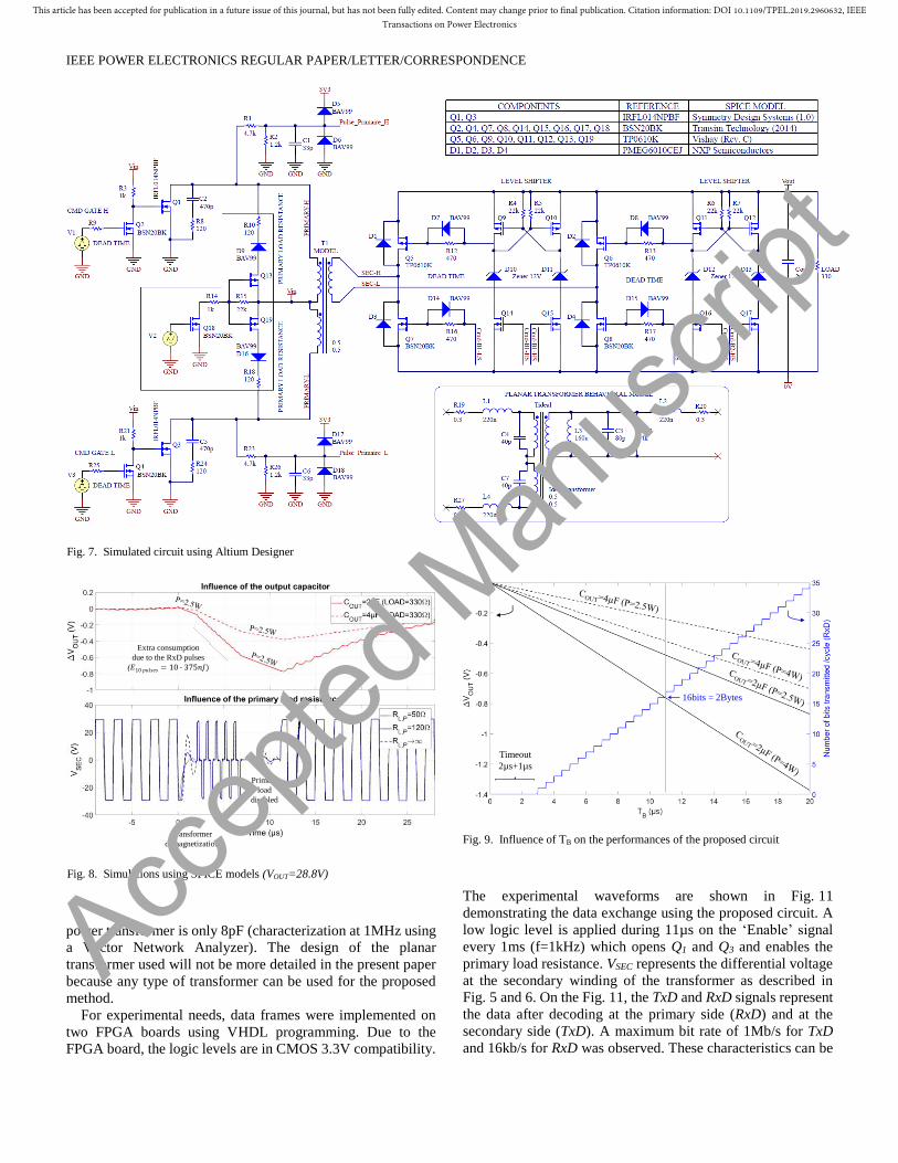
The circuit presented in Fig. 7 was simulated using SPICE
models for active components and a transformer behavioral
model. The references of the components used and the
associated SPICE models are given in the table presented in
Fig. 7. The supply transformer was realized by a planar
transformer integrated in a 6-layers board.
The simulations presented in Fig. 8 suggest an extra
consumption due to the RxD pulses during the demagnetizing
period. This effect is due to the ±15V applied on the primary
load resistances. The energy consumed by a single pulse E1 pulse
can be calculated using (1).
𝐸1 𝑝𝑢𝑙𝑠𝑒 = 𝑉𝐼𝑁
2
𝑅𝐿,𝑃∙ 𝑡𝑝𝑢𝑙𝑠𝑒 (1)
where RL,P is the primary load resistance. Since the positive
pulses are dissipated in the upper load resistance and the
negative ones are dissipated in the lower load resistance, the
resulting extra power consumption 𝑃𝑅𝑋𝐷 during TB can be
expressed as follows:
𝑃𝑅𝑋𝐷 = 𝑛 ∙ 𝑉𝐼𝑁
2
𝑅𝐿,𝑃 ∙ 𝑡𝑝𝑢𝑙𝑠𝑒
𝑇𝐵 (2)
where n is the number of RxD pulses, corresponding to the
number of changes in the logic levels (0→1 or 1→0). In the
worst case, n=(TB-3µs)/tbit=16 which leads to an additional
power consumption during TB of 545mW considering the
timing constraints proposed in section II. A.
As explained before, the demagnetizing oscillations can be
reduced depending on the primary load resistance seen by the
primary windings of the transformer. The influence of the
primary load resistance value on the demagnetizing is also
Fig. 5. Proposed communicating power supply circuit for gate driver application
En
En
Q7 Q8
Q5 Q6
VIN
VOUT’
Cmd
VOUT-REG’
COUT
[1:2]
VSEC’
load
En
RxD pulses generationManchester coding (TxD)
Q3
Q4
VIN
Q1
VIN
Q2
DC/DC
BUCK
load
LS
Level shifters
D3 D4
D2D1
0V 0V
RxDPulses
decoding
LPF
LPF
TxD
LPF
Manchester
decoding
Dead time
SN
UB
BE
R
SN
UB
BE
R
Re
f.
25V
+20V
-5V
5V
G
Kelvin
Gate driver application
Source
PW
M
Buffer
Accep
ted M
anus
cript

This article has been accepted for publication in a future issue of this journal, but has not been fully edited. Content may change prior to final publication. Citation information: DOI 10.1109/TPEL.2019.2960632, IEEETransactions on Power Electronics
IEEE POWER ELECTRONICS REGULAR PAPER/LETTER/CORRESPONDENCE
presented in Fig. 8. A low RL,P resistance can reduce the
demagnetizing oscillations but it would increase the power
consumption due to the RxD pulses. Based on simulations, the
primary load resistance was chosen RL,P=120Ω.
The main inconvenient of the proposed method is the output
voltage drop during the phase B due to the complete
demagnetization of the supply transformer. The duration of this
period is critical and should be reduced as much as possible.
Fortunately, the voltage drop can be compensated by adding
extra output capacitors COUT as shown in Fig. 9. As expressed
in (3), the observed variation ΔVOUT on the output voltage VOUT
is also dependant from the total power consumption P.
𝛥𝑉𝑂𝑈𝑇 = 𝑉𝑂𝑈𝑇 (𝑒−
𝑇𝐵𝑅𝐿𝑂𝐴𝐷∙𝐶𝑂𝑈𝑇 − 1) ≈ −
𝑃 ∙ 𝑇𝐵
𝑉𝑂𝑈𝑇 ∙ 𝐶𝑂𝑈𝑇 (3)
RLOAD is the equivalent resistance seen at the output. The
Fig. 9 illustrates the compromise between the RxD bit rate and
the dropout voltage at the output.
III. EXPERIMENTAL RESULTS
A. DATA exchange
A 6-layers Printed Circuit Board (PCB) was designed to
check the viability of the proposed method. The duration of the
phase B was fixed at TB=11µs in order to transmit 2 Bytes using
a 500ns bit time (=8µs) after the 2µs-deadtime. Once the
transmission is complete, another 1µs-deadtime was observed
in order to prevent any conflict.
The transformer used is a planar transformer with 5 turns in
the primary windings and 10 turns in the secondary winding.
As shown in Fig. 10, two planar transformers were integrated
in a 6-layers board (High Side and Low side) corresponding to
a Half-Bridge application. The planar transformer is a shell
form in which the magnetic core is realized by a E-shaped
ferrite core associated to a 3F3 ferromagnetic material. The
windings of the transformer are located on the internal layers of
the PCB. The electric isolation is realized by a 500µm epoxy-
layer, which guarantees a reliable isolation between primary
and secondary circuits. The resulting parasitic common mode
current is relatively low since the coupling capacitor of the
(a)
(b)
Fig. 6. Proposed communicating power supply circuit: (a) phase A and (b) phase B
Q5
D1
Q7
D3
VINVINEn
LO
AD
VOUT’
Cmd
’
VOUT-REG’ = 25V
COUT
[1:2]
VSEC’
TxDRxD
En
Manchester coding (TxD)
Q3
Q4
VIN
Q1
VIN
Q2
LPF
LPF
LPFManchester
decoding
0V 0V
Q6
D2
Q8
D4
En
Pulses
decoding
DC/DC
BUCK
TxD
A
Dead time
Q5
D1
Q7
D3
VINVINEn
LO
AD
VOUT’
Cmd
’
VOUT-REG’ = 25V
COUT
[1:2]
VSEC’
TxDRxD
En
Q3
Q4
VIN
Q1
VIN
Q2
LPF
LPF
LPFManchester
decoding
0V 0V
Q6
D2
Q8
D4
Level shifter Q5 Level shifter Q6
RxD pulses generation
DC/DC
BUCK
En
Pulses
decoding
RxD
B
RL,P
RL,P
Accep
ted M
anus
cript
This article has been accepted for publication in a future issue of this journal, but has not been fully edited. Content may change prior to final publication. Citation information: DOI 10.1109/TPEL.2019.2960632, IEEETransactions on Power Electronics
IEEE POWER ELECTRONICS REGULAR PAPER/LETTER/CORRESPONDENCE
power transformer is only 8pF (characterization at 1MHz using
a Vector Network Analyzer). The design of the planar
transformer used will not be more detailed in the present paper
because any type of transformer can be used for the proposed
method.
For experimental needs, data frames were implemented on
two FPGA boards using VHDL programming. Due to the
FPGA board, the logic levels are in CMOS 3.3V compatibility.
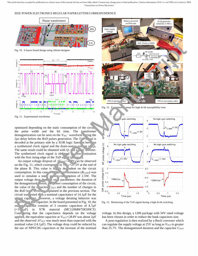
The experimental waveforms are shown in Fig. 11
demonstrating the data exchange using the proposed circuit. A
low logic level is applied during 11µs on the ‘Enable’ signal
every 1ms (f=1kHz) which opens Q1 and Q3 and enables the
primary load resistance. VSEC represents the differential voltage
at the secondary winding of the transformer as described in
Fig. 5 and 6. On the Fig. 11, the TxD and RxD signals represent
the data after decoding at the primary side (RxD) and at the
secondary side (TxD). A maximum bit rate of 1Mb/s for TxD
and 16kb/s for RxD was observed. These characteristics can be
Fig. 8. Simulations using SPICE models (VOUT=28.8V)
Extra consumption
due to the RxD pulses
(𝐸1 𝑒 = 1 𝑛 )
Transformer
demagnetization
Primary
load
disabled
Fig. 7. Simulated circuit using Altium Designer
Fig. 9. Influence of TB on the performances of the proposed circuit
16bits = 2Bytes
Timeout
2µs+1µs
Accep
ted M
anus
cript
This article has been accepted for publication in a future issue of this journal, but has not been fully edited. Content may change prior to final publication. Citation information: DOI 10.1109/TPEL.2019.2960632, IEEETransactions on Power Electronics
IEEE POWER ELECTRONICS REGULAR PAPER/LETTER/CORRESPONDENCE
optimized depending on the static consumption of the circuit,
the pulse width and the bit time. The transformer
demagnetization can be seen on the VSEC’ waveform during the
2µs delay before the RxD pulses generation. The TxD signal is
decoded at the primary side by a XOR logic function between
a synthetized clock signal and the drain-source voltage of Q8.
The same result could be obtained with Q7 and a logic inverter.
The synthetized clock signal is obtained by synchronization
with the first rising edge of the TxD signal (phase A).
An output voltage dropout of ΔVOUT=-0.8V can be observed
on the Fig. 11, which corresponds to VOUT=27.5V at the end of
the phase B. This value is highly dependent on the circuit
consumption. In this case, a 330Ω-load resistance (RLOAD) was
used to simulate a static power consumption of 2.5W. The
output voltage drop depends on 4 parameters: the duration of
the demagnetized period, the power consumption of the circuit,
the value of the capacitor COUT and the number of changes in
the RxD logic levels as explained in the previous section. The
circuit was tested with a nominal capacitance of 14.1µF for the
output capacitor. However, a voltage derating behavior was
observed on this capacitor. In the board presented in Fig. 10, the
output capacitor consists of 3 ceramic capacitors of 4.7µF
(=14.1µF) in X7R material (MC1206B475K500CT).
Considering that the capacitance depends on the voltage
applied, the equivalent capacitor at VOUT=28.8V was about 2µF
and the observed ΔVOUT was much more than expected with the
nominal value (14.1µF). The voltage drop could be reduced by
the use of NP0/C0G capacitors or the increase of the nominal
voltage. In this design, a 1206 package with 50V rated voltage
has been chosen in order to reduce the bank capacitors size.
A post-regulation is then realized by a Buck converter which
can regulate the supply voltage at 25V as long as VOUT is greater
than 25.7V. The demagnetized duration and the capacitor COUT
Fig. 11. Experimental waveforms
Fig. 10. 6-layers board design using Altium designer
Planar transformers
HS
LS
Fig. 12. Experimental setup for high dv/dt susceptibility tests
Diff. Probe (x1000)
dv/dt generatorHAEFELY P90.1
Battery poweredoscilloscope
Input supplyvoltage
FPGA (primary side) FPGA (secondary side)dv/dt
Battery
LOAD 330Ω
TxD
LPFManchester
decoding
RF probe
Secondary GND
isolation
Fig. 13. Monitoring of the TxD signal during a high dv/dt switching Accep
ted M
anus
cript

This article has been accepted for publication in a future issue of this journal, but has not been fully edited. Content may change prior to final publication. Citation information: DOI 10.1109/TPEL.2019.2960632, IEEETransactions on Power Electronics
IEEE POWER ELECTRONICS REGULAR PAPER/LETTER/CORRESPONDENCE
must be chosen considering the worst case scenario. In the
experimental setup, Artix-7 FPGA boards were used to manage
the communicating power supply circuit (FPGA board: Nexys4
DDR).
B. High dv/dt susceptibility tests
The gate driver boards are always implemented as close as
possible to the power modules in order to guarantee a correct
switching of the power device. Indeed, the parasitic inductances
of wires are sensitive to the common-mode currents. The power
circuit is often composed of several power devices in series or
parallel. In a half-bridge configuration, two power devices are
associated in series (HS and LS). During a fast switching of the
power component, a high dv/dt can be observed in the switch
node. In the gate driver boards, the secondary ground potential
is imposed by the source voltage which is a floating potential as
the source voltage of the HS component varies when the LS
power device is used. As a result, the gate drivers are submitted
to a severe environment with high EMI constraints.
In order to test the dv/dt susceptibility, high voltage pulsed
signals were applied between the primary ground and the
floating secondary ground [11], as shown in Fig. 12. In this
experiment, a battery-powered oscilloscope was used with
caution as high voltage transients were applied on the secondary
ground potential. The TxD signal was monitored during this
process in order to detect the perturbations on the internal
signals. The monitored signal is taken at the input of a Schmitt
triggered logic gate. The Schmitt triggers are very important in
this design as it can provide a reliable digital signal at the output
using the hysteresis principle. The tests were performed up to
Fig. 14. Experimental setup for evaluation under real switching conditions
Smart driver board (FPGA integration)
1.2kV SiCpower module
DC power supply
RF probe Differential probe
Busbar
L=700µH
Rogowski coilOscilloscope
Command circuit(double pulse)
Fig. 16. Experimental results using a 400V/200A switching cell
RxD
data
RxD
data
iD
(5mV/A)
VDS
VDS
iD
(5mV/A)
400V
400V
200A
200A
No logic gate switching
No logic gate switching
Turn-on
Turn-off(a)
(b)
Fig. 15. Smart driver board for health monitoring with embedded communication features. (a) top view, (b) bottom view
TOPD
G
S
D
G
S
HS
LS
BOTTOM
Accep
ted M
anus
cript
This article has been accepted for publication in a future issue of this journal, but has not been fully edited. Content may change prior to final publication. Citation information: DOI 10.1109/TPEL.2019.2960632, IEEETransactions on Power Electronics
IEEE POWER ELECTRONICS REGULAR PAPER/LETTER/CORRESPONDENCE
±125kV/µs applied across the isolation barrier. The signals
presented in Fig. 13 were taken at the secondary side using a
RF probe to minimize the noises due to the ground loop. In this
configuration, the oscilloscope must be referred at a floating
potential due to the fast pulses of 1.5kV applied on the isolation
barrier. The results presented in Fig. 13 demonstrate the
reliability of the proposed DATA communication system in the
worst case. The observed noise on the signals is the addition of
the real perturbation and the noise due to the probe. Since the
EMI noises are monitored in the worst case of study, the
threshold voltages of the Schmitt-triggered logic gates were
used to verify the integrity of the TxD signal when the EMI
noise occurs.
C. Implementation in a driver board design under real
switching conditions
As described in Fig. 14, a gate driver board was connected to
a 1.2kV SiC MOSFET module (Cree CAS300M12BM2) in a
double pulse test bench. The proposed solution was
implemented in a smart driver board which integrates Spartan-7
FPGA boards on the primary and secondary circuits, as shown
in Fig. 15 (b). This circuit was tested in a DC-DC Buck
configuration using an inductance of 700µH connected to the
busbar. An external gate resistance of 2.4Ω was implemented
on the gate driver board presented in Fig. 15. This board was
specifically designed for health monitoring and integrates the
proposed method as a communication channel in addition to
conventional features (galvanic isolation, short-circuit
detection, soft shut-down…). The design of this board will not
be more detailed in the present paper.
In the experimental setup, a differential probe and a
Rogowski coil were used to monitor the drain-source voltage
and the drain current of the power SiC MOSFET. As shown in
Fig. 16, a 400V/200A switching did not affect the RxD signal
at the primary side as no undesirable logic level change
occurred during the switching. The resulting dv/dt is about
15kV/µs which correspond to an optimal switching at 400V
considering the switching characteristics provided in the
CAS300M12BM2 datasheet (rise time of 68ns and fall time of
43ns).
IV. DISCUSSION AND PERSPECTIVES
As mentioned in the introduction, the targeted application is
health monitoring for power SiC MOSFET transistors. In this
case, the RxD data are monitoring parameters that can be
measured using the secondary circuit of a smart driver board
such as the on-state voltage, the gate leakage currents,
temperature values or others ageing indicators… The RxD data
could also be used for fault transmission by sending a more
detailed error message to the primary side. It could even replace
the traditional error pulse transmission but this solution is not
recommended as the latency of the proposed communication
method is not guaranteed. Another application is the
reparametrizing of the gate driver in real time which could be
achieved by exploiting the TxD flux. For example, switching
slope control, blanking time setting or gate-source voltage
variation could be realized using the proposed method. Other
applications such as the implementation of sensors on high
voltage lines could also be addressed.
Nowadays, gate drivers integrate more and more features and
FPGA/CPLD are already integrated on the primary circuit in
some designs. The addition of measurement and
communicating features on the gate drivers increases the
complexity, the cost and the size of the board which could be a
major constraint to the development of such technology.
However, the Fig. 15 demonstrates that it is possible to
integrate the proposed solution in a 120x70mm² design for
driving a 62mm power module. Moreover, the FPGA
integration is the first step in the prototyping process as most of
the circuitry presented in the Fig. 6 could be integrated in mixed
analog/digital chip designs.
V. CONCLUSION
A new structure for bidirectional DATA communication
using a low-power supply circuit was proposed and
investigated. The presented results show the relevance of the
proposed method in highly constraints gate driver designs. The
proposed structure was simulated and experimental results are
provided. Careful consideration should be given to the choice
of the output capacitors throughout the implementation of this
topology. In the implemented solution, bit rates of 1Mb/s for
TxD and 16kb/s for RxD were demonstrated. Fast transient
voltages were also applied on the designed board in order to
verify its dv/dt immunity up to 125kV/µs. The method was also
implemented in a smart gate driver board and confronted to a
400V/200A switching using a 1.2kV SiC module. The proposed
solution requires the integration of digital circuits on the gate
driver board but offers new perspectives for on-line monitoring
using the gate drivers in power electronics. A specific serial
protocol based on UART can be implemented for complex
DATA communication across the isolation barrier of the gate
driver boards. Due to the complexity and the cost of the health
monitoring using the gate driver, this technology might make
sense only for high power converters (>50kW) in which the
reliability is the priority.
REFERENCES
[1] T. A. Nguyen, S. Lefebvre, S. Azzopardi, “Effect of short circuit aging on
safe operating area of SiC MOSFET”, Microelectronics Reliability,
vol.88-90, p.645-651, 2018. [2] T. A. Nguyen, N. Boucenna, D. Labrousse, G. Chaplier, S. Lefebvre,
S.Azzopardi, “Investigation on Reliability of SiC MOSFET Under Long-
Term Extreme Operating Conditions”, PCIM Europe, 2018. [3] D. Othman, S. Lefebvre, M. Berkani, Z. Khatir, A. Ibrahim, A.
Bouzourene, “Robustness of 1.2 kV SiC MOSFET devices”,
Microelectronics Reliability, vol.53, p.1735-1738, 2013. [4] R. Ouaida, M. Berthou, J. León, X. Perpiñà, S. Oge, P. Brosselard, C.
Joubert, “Gate oxide Degradation of SiC MOSFET in Switching
conditions”, IEEE Electron Device Letters, vol. 35, p.1284-1286, 2014. [5] Z. Wang, X. Shi, L. M. Tolbert, F. Wang, Z. Liang, D. Costinett, B. J.
Blalock, “Temperature-dependent short-circuit capability of Silicon
Carbide power MOSFETs”, IEEE Transactions on Power Electronics, vol. 31, p. 1555-1566, 2016.
[6] S. Dusmez, B. Akin, “Remaining Useful Lifetime Estimation for
Degraded Power MOSFETs Under Cyclic Thermal Stress”, IEEE Energy Conversion Congress and Exposition (ECCE), 2015.
Accep
ted M
anus
cript

This article has been accepted for publication in a future issue of this journal, but has not been fully edited. Content may change prior to final publication. Citation information: DOI 10.1109/TPEL.2019.2960632, IEEETransactions on Power Electronics
IEEE POWER ELECTRONICS REGULAR PAPER/LETTER/CORRESPONDENCE
[7] N. Ginot, C. Batard, P. Lahaye, “MOSFET et IGBT : circuits de
commande, sécurisation et protection du composant à semi-conducteur”,
Tech. Ing., vol. V1, no. D3234, 2017.
[8] R. Herzer, “New Gate Driver Solutions for Modern Power Devices and
Topologies”, 9th International Conference on Integrated Power Electronics Systems (CIPS), 2016.
[9] A. Kumar, A. Ravichandran, S. Singh, S. Shah, S. Bhattacharya, “An
Intelligent Medium Voltage Gate Driver with Enhanced Short Circuit Protection Scheme for 10kV 4H-SiC MOSFETs”, IEEE Energy
Conversion Congress and Exposition (ECCE), 2017.
[10] A. Anurag, S. Acharya, G. Gohil, et S. Bhattacharya, “A Gate Driver Design for Medium Voltage Silicon Carbide Power Devices with High
dv/dt”, in IECON - 44th Annual Conference of the IEEE Industrial
Electronics Society, p. 877‑882, Oct. 2018. [11] J. Weckbrodt, N. Ginot, C. Batard, S. Azzopardi, “Short Pulse
Transmission for SiC Communicating Gate Driver Under High dv/dt”,
PCIM Europe, 2018. [12] C. Bouguet, N. Ginot, C. Batard, “Communicating Gate Driver for SiC
MOSFET”, PCIM Europe, 2016.
[13] Datasheet XTR26020, X-REL Semiconductor. [14] Datasheet Skyper Prime O, Semikron International GmbH.
[15] C. Bouguet, N. Ginot, C. Batard, “Communication Functions for a Gate
Driver Under High Voltage and High dv/dt”, IEEE Transactions on Power Electronics, vol. 33, 2018.
[16] J. Friebe, O. Prior, M. Kacki, “High-side driver supply with reduced
coupling capacitance”, PCIM Europe, 2018. [17] J. Wang, Z. Shen, C. DiMarino, R. Burgos, D. Boroyevich, “Gate Driver
Design for 1.7kV SiC MOSFET Module with Rogowski Current Sensor for Shortcircuit Protection”, IEEE Applied Power Electronics Conference
and Exposition (APEC), 2016.
[18] V.-S. Nguyen, L. Kerachev, P. Lefranc, J.-C. Crebier, “Characterization and Analysis of an Innovative Gate Driver and Power Supplies
Architecture for HF Power Devices with High dv/dt”, IEEE Trans. on
Power Electronics, vol. 32, p.6079-6090, 2017. [19] V.-S. Nguyen, P. Lefranc, J.-C. Crebier, “Gate Driver Supply
Architectures for Common Mode Conducted EMI Reduction in Series
Connection of Multiple Power Devices”, IEEE Trans. on Power Electronics, vol. 33, p. 10265-10276, Dec. 2018.
[20] W. Stefanutti, S. Saggini, P. Mattavelli, and M. Ghioni, “Power Line
Communication in Digitally Controlled DC–DC Converters Using Switching Frequency Modulation”, IEEE Trans. on Industrial
Electronics, vol. 55, no. 4, p. 1509‑1518, 2008.
[21] J. Jousse, N. Ginot, C. Batard, et E. Lemaire, “Power Line Communication Management of Battery Energy Storage in a Small-Scale
Autonomous Photovoltaic System”, IEEE Trans. Smart Grid, vol. 8, no.
5, p. 2129‑2137, Sept. 2017. [22] M. Yigit, V. C. Gungor, G. Tuna, M. Rangoussi, et E. Fadel, “Power line
communication technologies for smart grid applications: A review of
advances and challenges”, Comput. Netw., vol. 70, p. 366‑383, Sept. 2014.
[23] Ru-Shiuan Yang, Lon-Kou Chang, et Hung-Chi Chen, “An Isolated Full-
Bridge DC-DC Converter With 1-MHz Bidirectional Communication Channel”, IEEE Trans. on Industrial Electronics, vol. 58, no. 9, p.
4407‑4413, Sept. 2011.
[24] A. Volke and M. Hornkamp, “IGBT Modules. Technologies, Driver and Application”, Infineon Technologies, book, 2017.
[25] K. Kusaka et al., “Galvanic isolation system for multiple gate drivers with
inductive power transfer — Drive of three-phase inverter”, in IEEE Energy Conversion Congress and Exposition (ECCE), p. 4525‑4532,
2015.
[26] N. Rouger, L. T. Le, D. Colin, et J.-C. Crébier, “CMOS SOI gate driver with integrated optical supply and optical driving for fast power
transistors”, in 28th International Symposium on Power Semiconductor
Devices and ICs (ISPSD), p. 427‑430, 2016. [27] X. Zhang et al., “A 15 kV SiC MOSFET gate drive with power over fiber
based isolated power supply and comprehensive protection functions”,
IEEE Applied Power Electronics Conference and Exposition (APEC), March 2016.
Julien Weckbrodt was born in France in 1993. He
received the M.Sc.Eng. degree in electrical
engineering from the Polytechnical National Institute
(INP) of Bordeaux in 2016. He is currently working
toward the Ph.D. degree in electrical engineering at the University of Nantes, France. His work is supported
by Safran group.
His research interests include gate drivers, WBG power semiconductors, and electromagnetic
compatibility.
Nicolas Ginot was born in France, in 1977. He
received the B.S. degree in engineering from the Ecole Polytechnique de l’Université de Nantes, France, in
2001, and the Ph.D. degree in electrical engineering in
2004. From 2001 to 2007, he was with the industry on military and railway power electronic converters. He
is currently a Professor with the Institut Universitaire
de Technologie, Nantes, and the Institute of Electronics and Telecommunications of Rennes,
where he works on communicating system for power
electronic applications and smart drivers.
Christophe Batard was born in France, in 1965. He received the Ph.D. degree in electrical engineering
from the Institut National Polytechnique de Toulouse, Toulouse, France, in 1992. He was a Postdoctoral
Researcher with the University of Birmingham,
England, for one year, where he worked on the modeling of power diodes. In 1993, he joined the
Institut Universitaire de Technologie, Nantes, France,
as an Assistant Professor. He then conducted research with the Institute of Electronics and
Telecommunications of Rennes, where he works on
modeling of power converters, communicating system over high current, and power line communication in a power electronic environment.
Thanh-Long Le received the Engineer degree in
electrical engineering from the Hanoi University of
Science and Technology, Hanoi, Vietnam, in 2011, the M.S. degree in electrical engineering from the
Institut National Polytechnique de Grenoble,
Grenoble, France in 2012, and the Ph.D. degree in integrated gate driver for GaN components from
Grenoble Electrical Engineering Laboratory,
Université Grenoble Alpes, Grenoble, France, in 2015. He is currently a R&D Engineer at Safran Tech,
Safran Paris - Saclay. His research interests include
the gate driver for wide band gap power devices and the power module.
Stéphane Azzopardi received both the M.Sc.Eng. degree from the Graduate School of Engineering
INSA of Toulouse, France as well as the M.S. degree
from the University of Toulouse in 1993. He received the Ph.D. degree in electronics from the University of
Bordeaux in 1998. Then, he spent two years as post-
doctorate in the laboratory of Professor Kawamura at the Yokohama National University, Japan. In 2003, he
became Associate Professor at the Graduate School of
Engineering ENSEIRB-MATMECA in Bordeaux, France. In 2012, he received the HDR (qualification to
drive research activities). He joined the Research and Technology Center of
Safran Group in sept. 2015, where he manages the expert team on “Components, Power Modules and Materials”. His research works are focused
on the robustness and reliability of power semiconductor devices for
aeronautical applications.
Accep
ted M
anus
cript


