Embed Size (px)
Citation preview
1
A 71–86-GHz, Switchless, Asymmetric
Bidirectional Transceiver in 90-nm SiGe BiCMOSPo-Yi Wu, Student Member, IEEE, Tissana Kijsanayotin, Student Member, IEEE, and James F.
Buckwalter, Senior Member, IEEE
Abstract—An E-band (71–86-GHz) bidirectional transceiveris presented in this paper. The time-division duplex architectureavoids transmit/receive switches through the use of transistorbiasing in the signal path to minimize high-frequency loss.The low-noise amplifier (LNA) and power amplifier (PA) arecombined into a wideband PA/LNA circuit, which alleviates theparasitic loading of each circuit through a wideband powercombiner. The bidirectional transceiver circuit is implemented in90-nm SiGe BiCMOS process. In transmit mode, the bidirectionaltransceiver transmits a maximum saturated power of 11 dBm at78 GHz with a 3-dB bandwidth from 71 to 86 GHz. In receivemode, the maximum 30.6-dB conversion gain and the minimum6.6-dB noise figure are measured at 73 GHz. The whole RFfront-end chip consumes 350.2 mW and 137.7 mW dc powerin transmit and receive mode, respectively, including all the RF,IF and LO amplifiers. The overall chip size is 1.5 mm×0.9 mmincluding pads.
Index Terms—BiCMOS, bidirectional, low-noise amplifier,millimeter-wave, power amplifier, transceivers.
I. INTRODUCTION
ADVANCED silicon technologies have made millimeter-
wave (mm-wave) transceivers low cost for commercial
applications such as the 60-GHz short-range communications
[1], [2], E-band (71–76/81–86 GHz) long-range point-to-point
links [3], 24/77-GHz collision-avoidance automotive radars
[4], etc. At mm-wave bands, both Silicon CMOS (65-nm
CMOS with fT /fmax of 180/270 GHz [5]) and Silicon-
Germanium BiCMOS (130-nm SiGe HBT with fT /fmax of
230/300 GHz [6]) have been demonstrated for transceiver solu-
tions. Scaling of BiCMOS technologies still has the potential
to improve the CMOS and HBT performance (90-nm SiGe
HBT with fT /fmax of 310/340 GHz). An important feature
of a 90-nm BiCMOS process is that the 90-nm NMOS can be
incorporated into passive circuits at E-band. While the NMOS
is capable of operating in a mm-wave passive mixer, it has
significant loss as an RF switch.
A wideband transceiver RF front-end circuit is presented for
backhaul applications in E-band (71–76/81–86 GHz), long-
range cruise control automotive radars in 76–77 GHz, and
Manuscript submitted September 2015.P. Wu is with the Department of Electrical and Computer Engineering,
University of California at San Diego, La Jolla, CA 92093 USA (e-mail:[email protected]).
J. F. Buckwalter was with University of California at San Diego, La Jolla,CA 92093 USA. He is now with University of California at Santa Barbara,Santa Barbara, CA 93106 (e-mail: [email protected]).
Color versions of one or more of the figures in this paper are availableonline at http://ieeexplore.ieee.org.
Digital Object Identifier
Figure 1. An IF-shifting phased-array transceiver system.
short-range side-crash prevention radars in 77–81 GHz. The
proposed bidirectional transceiver could be incorporated into
an IF phase-shifting phased array as shown in Fig. 1. In
medium or long-range applications, a beamforming antenna
array is required for high directivity [7], [8]. Moreover,
half-duplex systems such as time-division duplexing (TDD)
communication and radar systems allow the transmitter and
receiver to share a single antenna element and make com-
pact bidirectional transceivers attractive in terms of area and
cost. Separate transmit (TX) / receive (RX) arrays double
the required silicon area. Therefore, bidirectional transceiver
elements have been proposed at 45-GHz [9] and 60-GHz
bands [10], however, no bidirectional transceivers have been
demonstrated at E-band to the author’s knowledge. Regardless
of BiCMOS scaling, the low-noise amplifier (LNA) and power
amplifier (PA) cannot be isolated with CMOS switches due
to the poor performance of the NMOS switch at E-band.
Consequently, this work develops a switchless bidirectional
interconnection of the PA and LNA.
In an IF phased-array system as shown in Fig. 1, the power
division occurs in the IF path in TX mode and splits the
power between each of the PAs requiring additional gain. In
RX mode, a passive mixer is desirable for higher linearity
before combining the signal at the IF band. Therefore, an
asymmetric bidirectional mixer is presented that can operate
as either an active or passive mixer. The system considerations
are described and motivation for the proposed transceiver
Digital Object Identifier: 10.1109/TMTT.2016.2608891
1557-9670 c© 2016 IEEE. Personal use is permitted, but republication/redistribution requires IEEE permission.See http://www.ieee.org/publications standards/publications/rights/index.html for more information.
2
architecture is discussed in Section II. Section III presents the
circuit implementations and the design details of each building
block. The measurement setup and results are reported in
Section VI.
II. SYSTEM CONSIDERATIONS FOR E-BAND
TRANSCEIVERS
Both 77-GHz automotive pulse-compression radar (PCR)
and the E-band (71–76/81–86-GHz) backhaul systems are
compatible with bandwidth up to 2 GHz. While many state-
of-the-art E-band point-to-point links use fixed high-gain
antennas to satisfy the link budget requirements, significant
commercial interest exists in scalable phased-array solutions
that provide electronically controllable beamsteering. Conse-
quently, recent works have investigated a number of beam-
forming architecture variations such as RF, LO, IF and base-
band phase shifting [11], [12].
RF phase-shifting configurations typically consume moder-
ate power and offer high linearity because the beam is formed
before the mixer and only one LO signal is required in the
transmitter or receiver [13], [14]. Since the phase shifters and
the power combiners/splitters are operated at the RF band,
the system budget, in terms of gain, noise figure (NF ), and
power become more stringent. The LO and IF phase-shifting
topologies avoid phase shifting in the RF signal path [8], [12].
The main challenge of these approaches is the distribution
of multiple LO signals with accurate phases at mm-wave
bands with low skew between the channels. In addition, the
LO spur could couple to the RF signal paths and result in
signal distortion. Baseband phased-array architectures adjust
the phase (delay) through digital signal processing and are
flexible for multiple-input-multiple-output (MIMO) systems
[1]. However, to implement a baseband-shifting system is still
challenging even if in advanced technologies since multiple
power-hungry and large dynamic range analog-to-digital con-
verters (ADCs) and digital-to-analog converters (DACs) are
required to process a huge amount of data.
An IF-shifting phased-array system as shown in Fig. 1 is
preferred because phase shifting occurs at a lower IF band.
There are advantages and disadvantages to the aforementioned
approaches, but IF phase shifting has the advantage of allowing
the scaling of the number of array elements by adding separate
transceiver chips and managing the beamforming at the IF
frequency. This makes the implementation of the phase shifters
at the IF band lower power and also allows for the formation
of multiple beams with multiple IF beamforming networks.
However, IF phase shifting requires a heterodyne transceiver
architecture with image rejection and requires both the LO
and RF signals to be split into in-phase and quadrature-
phase (I/Q) [15]. In a phased-array system, each sideband
suppression or image-rejection transceiver element not only
increases the circuit complexity, but also generates different
I/Q mismatch between each path. In this work, a frequency
plan is proposed using a fixed LO to mitigate the image
rejection while operating between 71 and 86 GHz. For 76
to 81-GHz automotive radar systems, the LO frequency is
chosen at 68 GHz, so the image band is located in 55–60
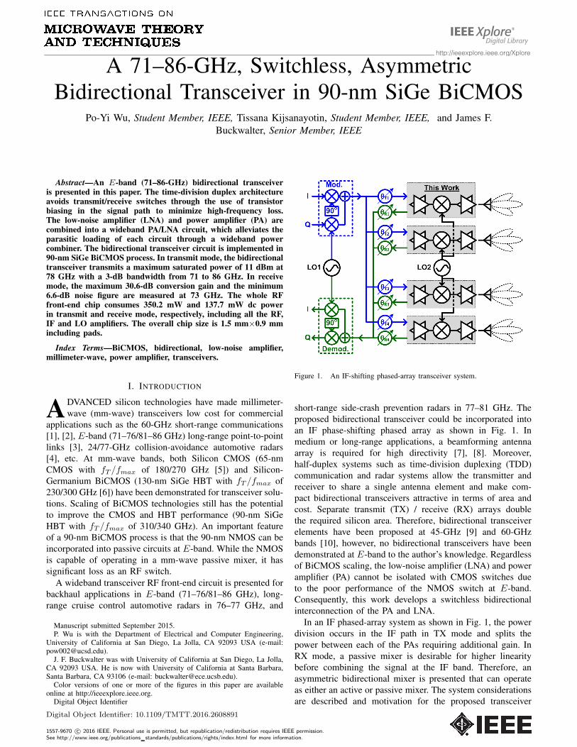
Figure 2. Proposed bidirectional transceiver block diagram.
GHz, which can highly attenuate the electromagnetic energy
by atmospheric oxygen [16]. This suggests that the IF would
range from 8 to 13 GHz for these radar systems. For an RF
signal in 71–76-GHz band, the IF band is between 3 and
8 GHz. For an RF signal in 81–86 GHz, the IF band is
between 13 and 18 GHz. The fixed LO architecture allows
beamformers that could be implemented at different IF bands
to cover different RF bands simultaneously.
In TX mode, the RF output power per element is determined
from
PTX = PIF –10 log10
N +GMIX +GPA, (1)
where PIF is the input IF power to an idealized IF beamformer
with 0-dB gain, N is the number of phased-array elements,
GMIX is the mixer conversion gain, and GPA is the PA gain.
Splitting the power into N paths effectively reduces the power
that reaches the mixer by a factor of N . To compensate more
gain is required at the mixer or the PA in order to drive the
PA to the saturated output power. As we discuss later, high PA
gain comes at a cost of potential instability for a bidirectional
front-end. Therefore, we investigate increasing the gain in the
mixer.
In RX mode, the IF output power with 0-dB beamformer
gain is determined from
PIF = PRX +GLNA +GMIX + 10 log10
N, (2)
where PRX is the received signal power per element and
GLNA is the LNA gain. The combined PIF is increased by
a factor of N . In this case, the linearity of the mixer is more
important to receive performance than gain. The input-referred
third-order intercept point (IIP3) of the RX is determined
from
1
IIP3,RX
=1
IIP3,LNA
+GLNA
IIP3,MIX
, (3)
where IIP3,LNA and IIP3,MIX are the individual IIP3
contributions of the LNA and mixer. This suggests that the
IIP3,MIX should be higher than the IIP3,LNA by a factor of
GLNA. As a result, the gain of the mixer should be sacrificed
for high linearity.
Fig. 2 shows the block diagram of the 71–76/81–86-GHz
(E-band) bidirectional transceiver front-end. The input stage
of the receiver is an LNA to amplify the signal received from
the antenna while minimizing the noise contribution of the
3
later stages. The output stage of the transmitter is a PA to
produce high output power. The LNA and PA both share
a common interface to the antenna port and mixer port. A
bidirectional mixer driven by a fixed LO amplifier is followed
by transmitter and receiver IF amplifiers.
There are two novel features in this work. First, we demon-
strate the implementation of a low-loss transmission-line-
based power splitting network that allows the LNA input and
PA output to be combined into a single port over a wide
bandwidth. By exploiting impedance variations at the LNA
input and the PA output, the transmission line lengths are
chosen to isolate one or the other for half-duplex operation.
Therefore, the PA/LNA combiner is proposed in this paper to
minimize the loading effect, while the PA/LNA is optimized
with 50-Ω loads to a single antenna and the bidirectional
mixer. Second, the implementation of the bidirectional mixer
is asymmetric (i.e. is operated as a passive or active mixer) to
give different conversion gain and linearity in the TX and RX
modes. The transmitter and receiver IF amplifiers compensate
the conversion loss of the mixer and are also combined at the
input and output. The input/output impedances of the turned-
OFF amplifiers are high enough at IF frequency, therefore,
switches or the proposed combiner are not required to isolate
the loading between each other.
III. CIRCUIT IMPLEMENTATIONS
A. 90-nm SiGe BiCMOS Process
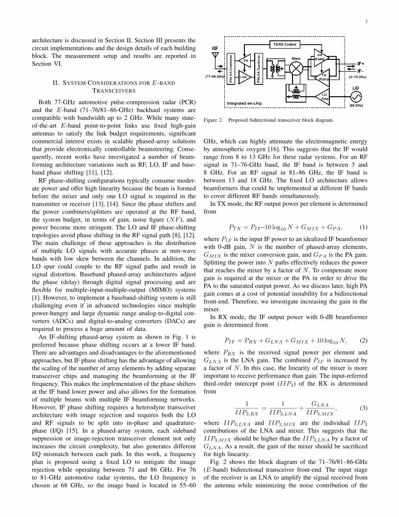
The 71–86-GHz bidirectional transceiver front-end is imple-
mented in a 90-nm SiGe BiCMOS process with nine copper
metal layers and one aluminum metal backend layer. A 4-
µm intrinsic HBT transistor operates at peak fT /fmax of
310/340 GHz at the bias current of 1.5–2.5 mA/µm as plotted
in Fig. 3. The extrinsic model for the transistor incorporates
the interconnection of the HBT transistor from M1 to the top
copper layer (OL) where the grounded coplanar waveguide
(GCPW) lines are fabricated. Considering the extrinsic inter-
connect parasitics, the peak fT /fmax drops to 280/320 GHz.
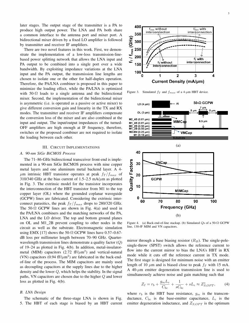
The 50-Ω GCPW lines are shown in Fig. 4(a) and used in
the PA/LNA combiners and the matching networks of the PA,
LNA and the LO driver. The top and bottom ground planes
on OL and M1_2B prevent coupling to other nodes in the
circuit as well as the substrate. Electromagnetic simulation
using EMX [17] shows the 50-Ω GCPW lines have 0.57–0.67-
dB loss per millimeter length between 70–90 GHz. Quarter-
wavelength transmission lines demonstrate a quality factor (Q)
of 19–24 as plotted in Fig. 4(b). In addition, metal-insulator-
metal (MIM) capacitors (2.72 fF/µm2) and vertical-natural
(VN) capacitors (0.94 fF/µm2) are fabricated in the back-end-
of-line of the process. The MIM capacitors are mainly used
as decoupling capacitors at the supply lines due to the higher
density and the lower Q, which helps the stability. In the signal
paths, VN capacitors are chosen due to the higher Q and lower
loss as plotted in Fig. 4(b).
B. LNA Design
The schematic of the three-stage LNA is shown in Fig.
5. The HBT of each stage is biased by an HBT current
Figure 3. Simulated fT and fmax of a 4-µm HBT device.
(a)
(b)
Figure 4. (a) Back-end-of-line stackup. (b) Simulated Qs of a 50-Ω GCPWline, 130-fF MIM and VN capacitors.
mirror through a base biasing resistor (RB). The single-pole-
single-throw (SPST) switch allows the reference current to
flow into the current mirror to bias the LNA’s HBT in RX
mode while it cuts off the reference current in TX mode.
The first stage is designed for minimum noise with an emitter
length of 10 µm and is biased close to peak fT with 15 mA.
A 40-µm emitter degeneration transmission line is used to
simultaneously achieve noise and gain matching such that
ZI = rb +gmLe
Cbe
+1
sCbe
+ sLe ≈ Z∗
S,OPT , (4)
where rb is the HBT base resistance, gm is the transcon-
ductance, Cbe is the base-emitter capacitance, Le is the
emitter degeneration inductance, and ZS,OPT is the optimum
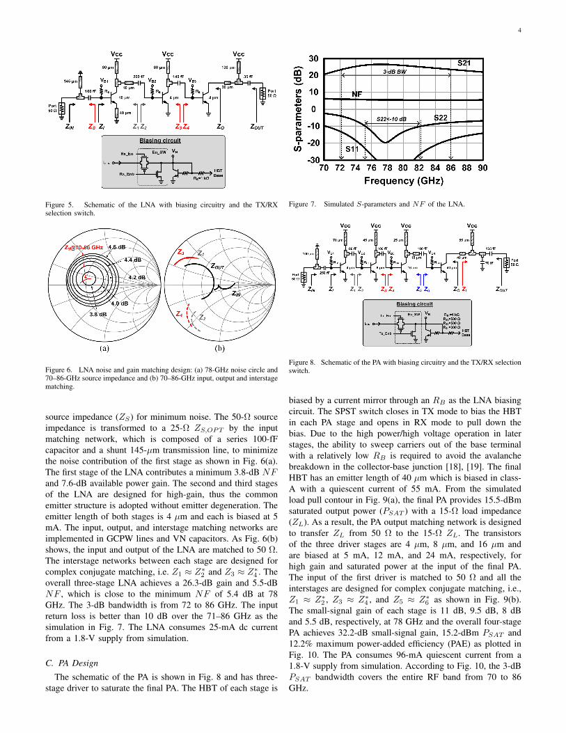
4
Figure 5. Schematic of the LNA with biasing circuitry and the TX/RXselection switch.
Figure 6. LNA noise and gain matching design: (a) 78-GHz noise circle and70–86-GHz source impedance and (b) 70–86-GHz input, output and interstagematching.
source impedance (ZS) for minimum noise. The 50-Ω source
impedance is transformed to a 25-Ω ZS,OPT by the input
matching network, which is composed of a series 100-fF
capacitor and a shunt 145-µm transmission line, to minimize
the noise contribution of the first stage as shown in Fig. 6(a).
The first stage of the LNA contributes a minimum 3.8-dB NFand 7.6-dB available power gain. The second and third stages
of the LNA are designed for high-gain, thus the common
emitter structure is adopted without emitter degeneration. The
emitter length of both stages is 4 µm and each is biased at 5
mA. The input, output, and interstage matching networks are
implemented in GCPW lines and VN capacitors. As Fig. 6(b)
shows, the input and output of the LNA are matched to 50 Ω.
The interstage networks between each stage are designed for
complex conjugate matching, i.e. Z1 ≈ Z∗
2and Z3 ≈ Z∗
4. The
overall three-stage LNA achieves a 26.3-dB gain and 5.5-dB
NF , which is close to the minimum NF of 5.4 dB at 78
GHz. The 3-dB bandwidth is from 72 to 86 GHz. The input
return loss is better than 10 dB over the 71–86 GHz as the
simulation in Fig. 7. The LNA consumes 25-mA dc current
from a 1.8-V supply from simulation.
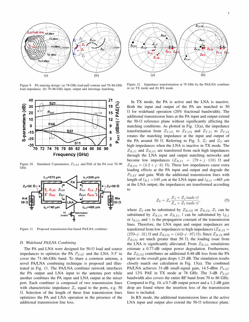
C. PA Design
The schematic of the PA is shown in Fig. 8 and has three-
stage driver to saturate the final PA. The HBT of each stage is
Figure 7. Simulated S-parameters and NF of the LNA.
Figure 8. Schematic of the PA with biasing circuitry and the TX/RX selectionswitch.
biased by a current mirror through an RB as the LNA biasing
circuit. The SPST switch closes in TX mode to bias the HBT
in each PA stage and opens in RX mode to pull down the
bias. Due to the high power/high voltage operation in later
stages, the ability to sweep carriers out of the base terminal
with a relatively low RB is required to avoid the avalanche
breakdown in the collector-base junction [18], [19]. The final
HBT has an emitter length of 40 µm which is biased in class-
A with a quiescent current of 55 mA. From the simulated
load pull contour in Fig. 9(a), the final PA provides 15.5-dBm
saturated output power (PSAT ) with a 15-Ω load impedance
(ZL). As a result, the PA output matching network is designed
to transfer ZL from 50 Ω to the 15-Ω ZL. The transistors
of the three driver stages are 4 µm, 8 µm, and 16 µm and
are biased at 5 mA, 12 mA, and 24 mA, respectively, for
high gain and saturated power at the input of the final PA.
The input of the first driver is matched to 50 Ω and all the
interstages are designed for complex conjugate matching, i.e.,
Z1 ≈ Z∗
2, Z3 ≈ Z∗
4, and Z5 ≈ Z∗
6as shown in Fig. 9(b).
The small-signal gain of each stage is 11 dB, 9.5 dB, 8 dB
and 5.5 dB, respectively, at 78 GHz and the overall four-stage
PA achieves 32.2-dB small-signal gain, 15.2-dBm PSAT and
12.2% maximum power-added efficiency (PAE) as plotted in
Fig. 10. The PA consumes 96-mA quiescent current from a
1.8-V supply from simulation. According to Fig. 10, the 3-dB
PSAT bandwidth covers the entire RF band from 70 to 86
GHz.
5
Figure 9. PA matcing design: (a) 78-GHz load-pull contour and 70–86-GHzload impedance. (b) 70–86-GHz input, output and interstage matching.
Figure 10. Simulated S-parameters, PSAT and PAE of the PA over 70–90GHz.
Figure 11. Proposed transmission-line-based PA/LNA combiner.
D. Wideband PA/LNA Combining
The PA and LNA were designed for 50-Ω load and source
impedances to optimize the PA PSAT and the LNA NF to
cover the 71–86-GHz band. To share a common antenna, a
novel PA/LNA combining technique is proposed and illus-
trated in Fig. 11. The PA/LNA combiner network interfaces
the PA output and LNA input to the antenna port while
another combines the PA input and LNA output at the mixer
port. Each combiner is composed of two transmission lines
with characteristic impedance Zo equal to the ports, e.g. 50
Ω. Selection of the length of these four transmission lines
optimizes the PA and LNA operation in the presence of the
additional transmission line loss.
Figure 12. Impedance transformation at 78 GHz by the PA/LNA combinerin (a) TX mode and (b) RX mode.
In TX mode, the PA is active and the LNA is inactive.
Both the input and output of the PA are matched to 50
Ω for wideband operation (20% fractional bandwidth). The
additional transmission lines at the PA input and output extend
the 50-Ω reference plane without significantly affecting the
matching conditions. As plotted in Fig. 12(a), the impedance
transformation from ZT,O1 to ZT,O2 and ZT,I1 to ZT,I2
rotates the matching impedance at the input and output of
the PA around 50 Ω. Referring to Fig. 5, ZI and ZO are
high impedances when the LNA is inactive in TX mode. The
ZR,I1 and ZR,O1 are transferred from such high impedances
through the LNA input and output matching networks and
become low impedances (ZR,I1 = (79 + j · 118) Ω and
ZR,O1 = (4.2 + j · 6) Ω). These low impedances cause extra
loading effects at the PA input and output and degrade the
PSAT and gain. With the additional transmission lines with
length of lR,I =145 µm at the LNA input and lR,O =465 µm
at the LNA output, the impedances are transformed according
to
Z2 = Zo
Z1 + Zo tanh γl
Zo + Z1 tanh γl, (5)
where Z2 can be substituted by ZR,O2 or ZR,I2, Z1 can be
substituted by ZR,O1 or ZR,I1, l can be substituted by lR,I
or lR,O, and γ is the propagation constant of the transmission
lines. Therefore, the LNA input and output impedances are
transferred from low impedances to high impedances (ZR,I2 =(270–j · 31) Ω and ZR,O2 = (442–j · 87) Ω). Since ZR,I2 and
ZR,O2 are much greater than 50 Ω, the loading issue from
the LNA is significantly alleviated. From ZR,I2, simulations
estimate a 0.77-dB output power degradation. Furthermore,
the ZR,O2 contributes an additional 0.48-dB loss from the PA
input so the overall gain drops 1.25 dB. The simulation results
closely match our calculation in Fig. 13(a). The combined
PA/LNA achieves 31-dB small-signal gain, 14.5-dBm PSAT
and 12% PAE in TX mode at 78 GHz. The 3-dB PSAT
bandwidth also covers the entire RF band from 70 to 86 GHz.
Compared to Fig. 10, a 0.7-dB output power and a 1.2-dB gain
drop are found where the insertion loss of the transmission
lines is included.
In RX mode, the additional transmission lines at the active
LNA input and output also extend the 50-Ω reference plane.
6
(a)
(b)
Figure 13. Combined PA/LNA simulation results. (a) S-parameters, PSAT
and PAE in TX mode. (b) S-parameters and NF in RX mode.
The input and output impedances are transferred from ZR,I1 to
ZR,I2 and ZR,O1 to ZR,O2 as shown in Fig. 12(b), and are still
matched to 50 Ω. Now, the PA is inactive and the lengths of
the input and output transmission lines are obtained as 245 µm
and 575 µm, respectively. Based on (5), the inactive PA input
and output impedances ZT,I1 = (6.8+j · 47) Ω and ZT,O1 =(6.7–j · 12) Ω are transferred to ZT,I2 = (566–j · 206) Ω and
ZT,O2 = (298–j · 48) Ω. Due to the ZT,I2, a 0.37-dB loss is
introduced at the LNA output. From ZT,O2, the LNA input has
a 0.69-dB loss, which also introduces a NF degradation, and
results in overall 1.06-dB gain lower. The simulation in Fig.
13(b) demonstrates the combined PA/LNA achieves 25.2-dB
gain and 6.26-dB NF at 78 GHz in RX mode. Comparing to
Fig. 7, 1.1-dB gain and 0.76-dB NF degradations are found
from the insertion loss of the transmission lines and the loading
effect of the PA.
It is notable that the PA and LNA form feedback paths to
each other and may cause instability. In the RX mode, the
feedback path is isolated by disabling the PA bias. In TX
mode, however, the feedback path formed by the LNA may
not be well isolated. Even if the LNA is inactive, the active
PA drives a high output power/voltage and is likely to drive
the Vbe of the input LNA HBT greater than VT . As a result, a
shunt switch is designed at the collector node of the third stage
of LNA HBT to improve the PA/LNA reverse isolation (S12)
in TX mode. The OFF resistance and capacitance (ROFF and
Figure 14. Simulated (a) S12, (b) K-factor and B1-factor of the combinedPA/LNA in TX mode.
COFF ) of this shunt switch causes ~0.2-dB loss in RX mode
in 70–90 GHz and insignificantly impacts NF . Fig. 14(a) plots
the S12 of the combined PA/LNA in TX mode. S12 is greatly
improved by the shunt switch due to the reduced feedback by
the LNA. The stability factors prove the stability improvement
as plotted in Fig. 14(b). Without the switch, the K-factor is
close to unity in 95 GHz, so that the PA is likely to become
conditionally stable. With the shunt switch, the unconditionally
stable is ensured since K > 1 and B1 > 0 over frequency.
In RX mode, the LNA is turned on by biasing up the HBT
base through the SPST shown in Fig. 5. Alternatively, the PA
HBT is biased by enabling the reference current through the
SPST shown in Fig. 8. Therefore, the TX/RX mode transition
time is determined by the step response of the HBT base
biasing circuitry. For instance, the settling time of enabling
TX mode is dominated by the largest RB and input series
capacitance at the first stage of PA. It can be found that
charging the 250-fF capacitor through the 1-kΩ RB1 takes
~1.2 ns to reach 99% base bias voltage from 0 V. Similarly,
the settling time of enabling RX mode is dominated by the
second stage of LNA. Therefore, the TX and RX can reach
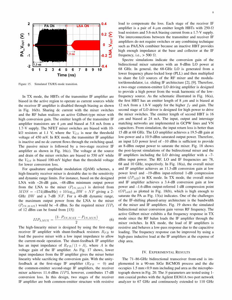
stable gain level within 1.3 ns as the simulated waveform in
Fig. 15, where PA and LNA input power is –10 dBm and –30
dBm respectively.
E. Mixer, IF and LO Amplifiers
In TX mode, an active mixer is preferred over a passive
mixer to provide higher conversion gain to drive the PA.
Additionally, the power division in the phased array transmitter
splits between each of the PAs requiring additional gain. In RX
mode, a passive mixer is desirable for higher linearity before
combining the signal at the IF band. Therefore, a bidirectional
mixer is proposed in this work based on a single FET quad
that can be operated as a passive mixer (i.e. zero dc current) in
the RX mode or as an active mixer (i.e. non-zero dc current)
in TX mode.
The double-balanced mixing stage consists of four NFETs
arranged in a switching quad as shown in Fig. 16(a) and is
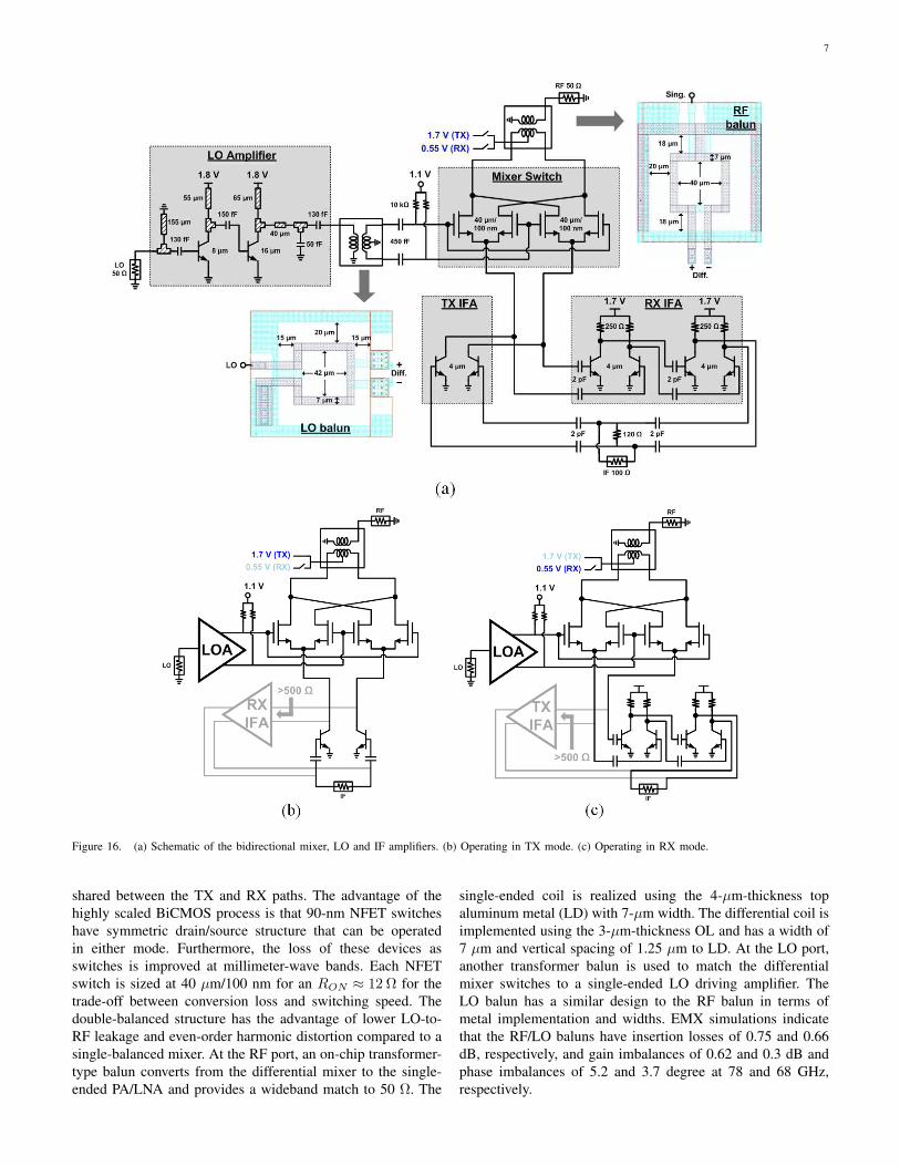
7
Figure 16. (a) Schematic of the bidirectional mixer, LO and IF amplifiers. (b) Operating in TX mode. (c) Operating in RX mode.
shared between the TX and RX paths. The advantage of the
highly scaled BiCMOS process is that 90-nm NFET switches
have symmetric drain/source structure that can be operated
in either mode. Furthermore, the loss of these devices as
switches is improved at millimeter-wave bands. Each NFET
switch is sized at 40 µm/100 nm for an RON ≈ 12 Ω for the
trade-off between conversion loss and switching speed. The
double-balanced structure has the advantage of lower LO-to-
RF leakage and even-order harmonic distortion compared to a
single-balanced mixer. At the RF port, an on-chip transformer-
type balun converts from the differential mixer to the single-
ended PA/LNA and provides a wideband match to 50 Ω. The
single-ended coil is realized using the 4-µm-thickness top
aluminum metal (LD) with 7-µm width. The differential coil is
implemented using the 3-µm-thickness OL and has a width of
7 µm and vertical spacing of 1.25 µm to LD. At the LO port,
another transformer balun is used to match the differential
mixer switches to a single-ended LO driving amplifier. The
LO balun has a similar design to the RF balun in terms of
metal implementation and widths. EMX simulations indicate
that the RF/LO baluns have insertion losses of 0.75 and 0.66
dB, respectively, and gain imbalances of 0.62 and 0.3 dB and
phase imbalances of 5.2 and 3.7 degree at 78 and 68 GHz,
respectively.
8
Figure 15. Simulated TX/RX-mode transition.
In TX mode, the HBTs of the transmitter IF amplifier are
biased in the active region to operate as current sources while
the receiver IF amplifier is disabled through biasing as shown
in Fig. 16(b). Sharing dc current with the mixer switches
and the RF balun realizes an active Gilbert-type mixer with
high conversion gain. The emitter length of the transmitter IF
amplifier transistors are 4 µm and biased at 5.8 mA from a
1.7-V supply. The NFET mixer switches are biased with 10-
kΩ resistors at 1.1 V, where the VGS is near the threshold
voltage of 450 mV. In RX mode, the transmitter IF amplifier
is inactive and no dc current flows through the switching quad.
The passive mixer is followed by a two-stage receiver IF
amplifier as shown in Fig. 16(c). The voltage at the source
and drain of the mixer switches are biased to 550 mV while
the VGS is biased 100-mV higher than the threshold voltage
for lower conversion loss.
For quadrature amplitude modulation (QAM) schemes, a
high-linearity receiver mixer is desirable due to the sensitivity
and dynamic range limits. For instance, based on the designed
LNA with ~26-dB gain, –48-dBm minimum output power
from the LNA to the mixer (PIN,MIN ) is derived from
MDS = –174(dBm/Hz) + 10 log10
BW + NF giving a 2-
GHz BW and a 7-dB NF . For a 40-dB dynamic range,
the maximum output power from the LNA to the mixer
(PIN,MAX ) would be –8 dBm. So the required mixer IIP3
of 12 dBm can be found from [15]:
IIP3,MIX =(3 · PIN,MAX − PIN,MIN )
2. (6)
The high-linearity mixer is designed by using the first-stage
receiver IF amplifier with shunt-feedback resistors RFB to
load the passive mixer with a low input impedance to allow
the current-mode operation. The shunt-feedback IF amplifier
has an input impedance of RFB/ (1 +A), where A is the
voltage gain of the IF amplifier. As Fig. 17 shows, lower
input impedance from the IF amplifier gives the mixer better
linearity while sacrificing the conversion gain. With the unity-
feedback at the first-stage IF amplifier (RFB = 0) and
the common-emitter second-stage IF amplifiers, the receiver
mixer achieves 11.4-dBm IIP3, however, contributes 17-dB
conversion loss. In this design, two stages of the receiver
IF amplifier are both common-emitter structure with resistive
load to compensate the loss. Each stage of the receiver IF
amplifier is a pair of 4-µm emitter length HBTs with 250-Ωload resistors and 5.6-mA biasing current from a 1.7-V supply.
The interconnections between the transmitter and receiver IF
amplifiers do not require switches or any combining technique
such as PA/LNA combiner because an inactive HBT provides
high enough impedance at the base and collector at the IF
frequency, i.e., > 500 Ω.
Spectre simulations indicate the conversion gain of the
bidirectional mixer saturates with an 8-dBm LO power at
68 GHz. In general, the 68-GHz LO is generated from a
lower frequency phase-locked loop (PLL) and then multiplied
to share the LO sources of the RF mixer and the modula-
tor/demodulator, i.e. sliding IF architecture [2], [9]. Therefore,
a two-stage common-emitter LO driving amplifier is designed
to provide a high power from the weak harmonic of the low-
frequency source. As the schematic illustrated in Fig. 16(a),
the first HBT has an emitter length of 8 µm and is biased at
12 mA from a 1.8-V supply for the higher fT and gain. The
second stage of LO driver is designed for high power to drive
the mixer switches. The emitter length of second HBT is 16
µm and biased at 24 mA. The input, output and interstage
matching networks are implemented in GCPW lines and VN
capacitors. From simulation, the input return loss is better than
15 dB at 68 GHz. The LO amplifier achieves a 19.5-dB gain at
low-power and a 10.9-dBm saturated output power. Therefore,
an input LO power level of –10 dBm is sufficient to provide
an 8-dBm output power to saturate the mixer. Fig. 18 shows
the post-layout simulations of the bidirectional mixer and the
IF amplifiers including the LO driving amplifier with a –7-
dBm input power. The RF, LO and IF frequencies are 78,
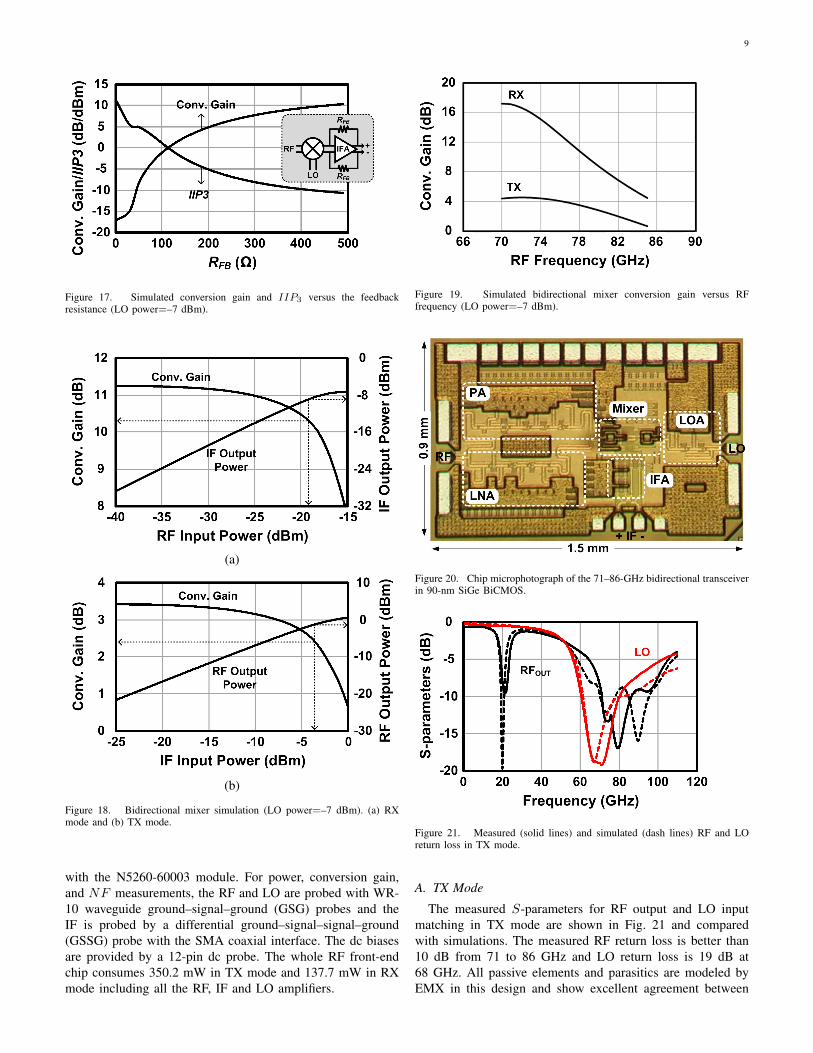
68 and 10 GHz, respectively. In Fig. 18(a), the overall mixer
and IF amplifier achieves an 11.3-dB conversion gain at low
power level and –19-dBm input-referred 1-dB compression
point (IP1dB) in RX mode. In TX mode, the overall mixer
and IF amplifier achieves a 3.4-dB conversion gain at low
power and –1.6-dBm output-referred 1-dB compression point
(OP1dB) as plotted in Fig. 18(b), which is high enough to
saturate the PA as Fig. 13(a) indicates. One of the challenges
of the IF-shifting phased-array architecture is the bandwidth
of the mixer and IF amplifiers. Fig. 19 shows the simulated
bidirectional mixer conversion gain versus RF frequency. The
active Gilbert mixer exhibits a flat frequency response in TX
mode since the RF balun loads the IF amplifier through the
mixer switches. In RX mode, the load of IF amplifiers is
resistive and behaves a low-pass response due to the capacitive
loading. The frequency response can be improved by using a
high-pass inductive load at the IF amplifiers at the expense of
chip area.
IV. EXPERIMENTAL RESULTS
The 71–86-GHz bidirectional transceiver front-end is im-
plemented in a 90-nm SiGe BiCMOS process and the die
occupies 1.5 mm×0.9 mm including pad area as the micropho-
tograph shown in Fig. 20. The S-parameters are tested using 1-
mm coaxial probes with the Agilent E8361A two port network
analyzer to 67 GHz and continuously extended to 110 GHz
9
Figure 17. Simulated conversion gain and IIP3 versus the feedbackresistance (LO power=–7 dBm).
(a)
(b)
Figure 18. Bidirectional mixer simulation (LO power=–7 dBm). (a) RXmode and (b) TX mode.
with the N5260-60003 module. For power, conversion gain,
and NF measurements, the RF and LO are probed with WR-
10 waveguide ground–signal–ground (GSG) probes and the
IF is probed by a differential ground–signal–signal–ground
(GSSG) probe with the SMA coaxial interface. The dc biases
are provided by a 12-pin dc probe. The whole RF front-end
chip consumes 350.2 mW in TX mode and 137.7 mW in RX
mode including all the RF, IF and LO amplifiers.
Figure 19. Simulated bidirectional mixer conversion gain versus RFfrequency (LO power=–7 dBm).
Figure 20. Chip microphotograph of the 71–86-GHz bidirectional transceiverin 90-nm SiGe BiCMOS.
Figure 21. Measured (solid lines) and simulated (dash lines) RF and LOreturn loss in TX mode.
A. TX Mode
The measured S-parameters for RF output and LO input
matching in TX mode are shown in Fig. 21 and compared
with simulations. The measured RF return loss is better than
10 dB from 71 to 86 GHz and LO return loss is 19 dB at
68 GHz. All passive elements and parasitics are modeled by
EMX in this design and show excellent agreement between
10
Figure 22. Measured conversion gain, PSAT and LO leakage at 78-GHzRF frequency in TX mode.
simulation and measurement.
For the power measurement, the RF output power is sensed
by an Agilent W8486A power sensor and read by an Agilent
E4419B power meter. The LO signal is generated from Agilent
E8257D and is multiplied using a Pacific Millimeter E3 tripler
to 68 GHz. The IF signal is provided by another Agilent
E8257D signal generator and is converted to differential by a
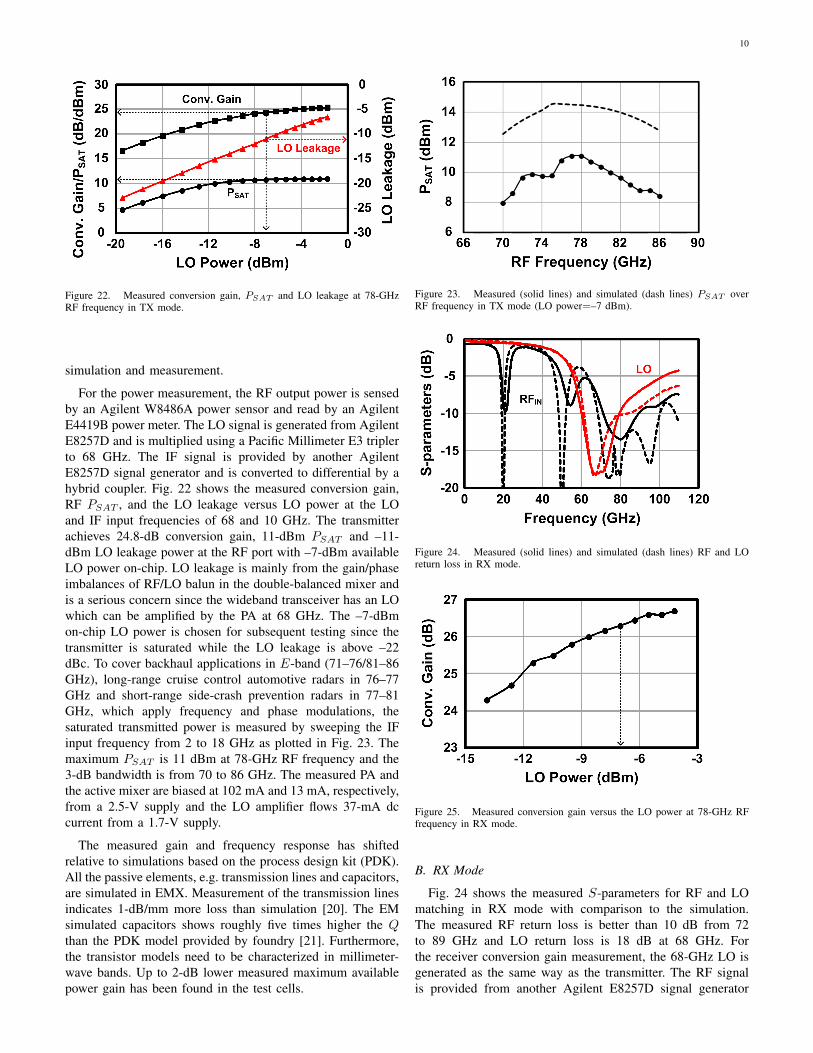
hybrid coupler. Fig. 22 shows the measured conversion gain,
RF PSAT , and the LO leakage versus LO power at the LO
and IF input frequencies of 68 and 10 GHz. The transmitter
achieves 24.8-dB conversion gain, 11-dBm PSAT and –11-
dBm LO leakage power at the RF port with –7-dBm available
LO power on-chip. LO leakage is mainly from the gain/phase
imbalances of RF/LO balun in the double-balanced mixer and
is a serious concern since the wideband transceiver has an LO
which can be amplified by the PA at 68 GHz. The –7-dBm
on-chip LO power is chosen for subsequent testing since the
transmitter is saturated while the LO leakage is above –22
dBc. To cover backhaul applications in E-band (71–76/81–86
GHz), long-range cruise control automotive radars in 76–77
GHz and short-range side-crash prevention radars in 77–81
GHz, which apply frequency and phase modulations, the
saturated transmitted power is measured by sweeping the IF
input frequency from 2 to 18 GHz as plotted in Fig. 23. The
maximum PSAT is 11 dBm at 78-GHz RF frequency and the
3-dB bandwidth is from 70 to 86 GHz. The measured PA and
the active mixer are biased at 102 mA and 13 mA, respectively,
from a 2.5-V supply and the LO amplifier flows 37-mA dc
current from a 1.7-V supply.
The measured gain and frequency response has shifted
relative to simulations based on the process design kit (PDK).
All the passive elements, e.g. transmission lines and capacitors,
are simulated in EMX. Measurement of the transmission lines
indicates 1-dB/mm more loss than simulation [20]. The EM
simulated capacitors shows roughly five times higher the Qthan the PDK model provided by foundry [21]. Furthermore,
the transistor models need to be characterized in millimeter-
wave bands. Up to 2-dB lower measured maximum available
power gain has been found in the test cells.
Figure 23. Measured (solid lines) and simulated (dash lines) PSAT overRF frequency in TX mode (LO power=–7 dBm).
Figure 24. Measured (solid lines) and simulated (dash lines) RF and LOreturn loss in RX mode.
Figure 25. Measured conversion gain versus the LO power at 78-GHz RFfrequency in RX mode.
B. RX Mode
Fig. 24 shows the measured S-parameters for RF and LO
matching in RX mode with comparison to the simulation.
The measured RF return loss is better than 10 dB from 72
to 89 GHz and LO return loss is 18 dB at 68 GHz. For
the receiver conversion gain measurement, the 68-GHz LO is
generated as the same way as the transmitter. The RF signal
is provided from another Agilent E8257D signal generator
11
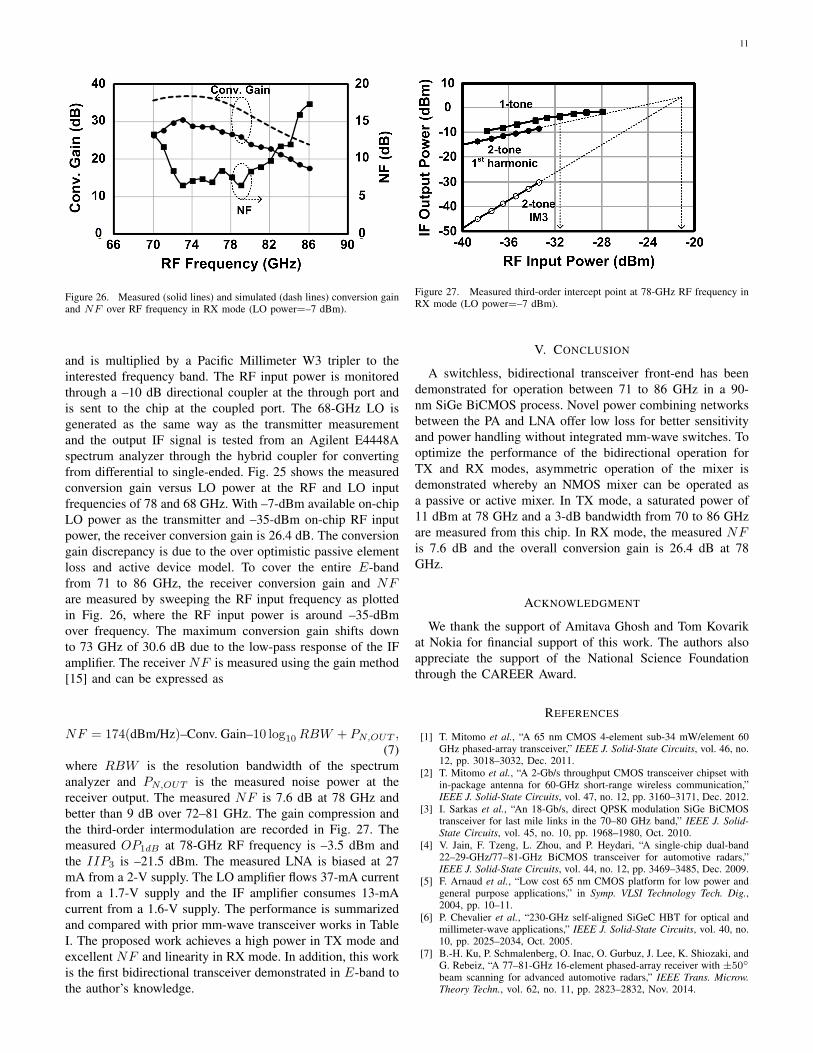
Figure 26. Measured (solid lines) and simulated (dash lines) conversion gainand NF over RF frequency in RX mode (LO power=–7 dBm).
and is multiplied by a Pacific Millimeter W3 tripler to the
interested frequency band. The RF input power is monitored
through a –10 dB directional coupler at the through port and
is sent to the chip at the coupled port. The 68-GHz LO is
generated as the same way as the transmitter measurement
and the output IF signal is tested from an Agilent E4448A
spectrum analyzer through the hybrid coupler for converting
from differential to single-ended. Fig. 25 shows the measured
conversion gain versus LO power at the RF and LO input
frequencies of 78 and 68 GHz. With –7-dBm available on-chip
LO power as the transmitter and –35-dBm on-chip RF input
power, the receiver conversion gain is 26.4 dB. The conversion
gain discrepancy is due to the over optimistic passive element
loss and active device model. To cover the entire E-band
from 71 to 86 GHz, the receiver conversion gain and NFare measured by sweeping the RF input frequency as plotted
in Fig. 26, where the RF input power is around –35-dBm
over frequency. The maximum conversion gain shifts down
to 73 GHz of 30.6 dB due to the low-pass response of the IF
amplifier. The receiver NF is measured using the gain method
[15] and can be expressed as
NF = 174(dBm/Hz)–Conv. Gain–10 log10
RBW + PN,OUT ,(7)
where RBW is the resolution bandwidth of the spectrum
analyzer and PN,OUT is the measured noise power at the
receiver output. The measured NF is 7.6 dB at 78 GHz and
better than 9 dB over 72–81 GHz. The gain compression and
the third-order intermodulation are recorded in Fig. 27. The
measured OP1dB at 78-GHz RF frequency is –3.5 dBm and
the IIP3 is –21.5 dBm. The measured LNA is biased at 27
mA from a 2-V supply. The LO amplifier flows 37-mA current
from a 1.7-V supply and the IF amplifier consumes 13-mA
current from a 1.6-V supply. The performance is summarized
and compared with prior mm-wave transceiver works in Table
I. The proposed work achieves a high power in TX mode and
excellent NF and linearity in RX mode. In addition, this work
is the first bidirectional transceiver demonstrated in E-band to
the author’s knowledge.
Figure 27. Measured third-order intercept point at 78-GHz RF frequency inRX mode (LO power=–7 dBm).
V. CONCLUSION
A switchless, bidirectional transceiver front-end has been
demonstrated for operation between 71 to 86 GHz in a 90-
nm SiGe BiCMOS process. Novel power combining networks
between the PA and LNA offer low loss for better sensitivity
and power handling without integrated mm-wave switches. To
optimize the performance of the bidirectional operation for
TX and RX modes, asymmetric operation of the mixer is
demonstrated whereby an NMOS mixer can be operated as
a passive or active mixer. In TX mode, a saturated power of
11 dBm at 78 GHz and a 3-dB bandwidth from 70 to 86 GHz
are measured from this chip. In RX mode, the measured NFis 7.6 dB and the overall conversion gain is 26.4 dB at 78
GHz.
ACKNOWLEDGMENT
We thank the support of Amitava Ghosh and Tom Kovarik
at Nokia for financial support of this work. The authors also
appreciate the support of the National Science Foundation
through the CAREER Award.
REFERENCES
[1] T. Mitomo et al., “A 65 nm CMOS 4-element sub-34 mW/element 60GHz phased-array transceiver,” IEEE J. Solid-State Circuits, vol. 46, no.12, pp. 3018–3032, Dec. 2011.
[2] T. Mitomo et al., “A 2-Gb/s throughput CMOS transceiver chipset within-package antenna for 60-GHz short-range wireless communication,”IEEE J. Solid-State Circuits, vol. 47, no. 12, pp. 3160–3171, Dec. 2012.
[3] I. Sarkas et al., “An 18-Gb/s, direct QPSK modulation SiGe BiCMOStransceiver for last mile links in the 70–80 GHz band,” IEEE J. Solid-
State Circuits, vol. 45, no. 10, pp. 1968–1980, Oct. 2010.
[4] V. Jain, F. Tzeng, L. Zhou, and P. Heydari, “A single-chip dual-band22–29-GHz/77–81-GHz BiCMOS transceiver for automotive radars,”IEEE J. Solid-State Circuits, vol. 44, no. 12, pp. 3469–3485, Dec. 2009.
[5] F. Arnaud et al., “Low cost 65 nm CMOS platform for low power andgeneral purpose applications,” in Symp. VLSI Technology Tech. Dig.,2004, pp. 10–11.
[6] P. Chevalier et al., “230-GHz self-aligned SiGeC HBT for optical andmillimeter-wave applications,” IEEE J. Solid-State Circuits, vol. 40, no.10, pp. 2025–2034, Oct. 2005.
[7] B.-H. Ku, P. Schmalenberg, O. Inac, O. Gurbuz, J. Lee, K. Shiozaki, andG. Rebeiz, “A 77–81-GHz 16-element phased-array receiver with ±50
beam scanning for advanced automotive radars,” IEEE Trans. Microw.
Theory Techn., vol. 62, no. 11, pp. 2823–2832, Nov. 2014.
12
Table IPERFORMANCE SUMMARY AND COMPARISON OF PUBLISHED MM-WAVE TRANSCEIVERS.
Reference This work [10] [9] [4] [22] [23] [24]
Technology90-nm SiGe
90-nm CMOS120-nm SiGe 180-nm SiGe
65-nm CMOS130-nm SiGe 130-nm SiGe
BiCMOS BiCMOS BiCMOS BiCMOS BiCMOS
Frequency 71–86 GHz 60 GHz 41–46 GHz 77–81 GHz 76–76.7 GHz 70–80 GHz 71–76 GHz
Description TRx Element 4-Element TRx TRx Element TRx TRx TRx TRx
Chip Area 1.5×0.9 mm2 1.6×1 mm2 1.6×0.8 mm2 3.9×1.9 mm2 1.03×0.94 mm2 1.9×1.1 mm2 5.2×1.7 mm2
TX Mode
Conversion Gain 24.8 dB 7 dB 35 dB 10 dB 15.1 dB – 33 dB
OP1dB 9.3 dBm 0.5 dBm 8.5 dBm 10.5 dBm – – 18 dBm
PSAT 11 dBm 3.5 dBm 9.5 dBm – 6.4 dBm 9 dBm 21 dBm
DC Power 350.2 mW 78 mW 119.4 mW 332.5 mW 187 mWa 621 mW 1740 mW
RX Mode
Conversion Gain 26.4 dB 7 dB 34 dB 31 dB 23 dB 50 dB 65 dB
NF 7.6 dB 8.7 dB 4.7 dB 8 dB 14.8 dB 7 dB 6 dB
OP1dB –3.5 dBm –13 dBm –5 dBm –0.7 dBm – –2 dBm 0 dBm
IIP3 –21.5 dBm – –26.3 dBm – – – –
DC Power 137.7 mW 78 mW 54 mW 162.5 mW 20 mWb 424 mW 540 mWaPA onlybLNA only
[8] A. Natarajan, A. Komijani, G. Xiang, A. Babakhani, and A. Hajimiri,"A 77-GHz phased-array transceiver with on-chip antennas in silicon:transmitter and local LO-path phase shifting," IEEE J. Solid-State
Circuits, vol.41, no.12, pp.2807–2819, Dec. 2006.
[9] J. Kim, and J. F. Buckwalter, “A switchless, Q-Band bidirectionaltransceiver in 0.12-µm SiGe BiCMOS technology,“ IEEE J. Solid-State
Circuits, vol.47, no.2, pp. 368–380, Feb. 2012.
[10] E. Cohen, C. Jakobson, S. Ravid, and D. Ritter, “A bidirectional TX/RXfour-element phased array at 60 GHz with RF-IF conversion block in90-nm CMOS process,” IEEE Trans. Microw. Theory Techn., vol. 58,no. 5, pp. 1438–1446, May 2010.
[11] L. Wu, A. Li, and H. C. Luong, “A 4-path 42.8-to-49.5 GHz LO gener-ation with automatic phase tuning for 60 GHz phased-array receivers,“IEEE J. Solid-State Circuits, vol.48, no.10, pp. 2309–2322, Oct. 2013.
[12] H. Hashemi, X. Guan, A. Komijani, and A. Hajimiri, “A 24-GHzSiGe phased-array receiver–LO phase shifting approach,” IEEE Trans.
Microw. Theory Techn., vol. 53, no. 2, pp. 614–626, Feb. 2005.
[13] A. Natarajan et al., “A fully-integrated 16-element phased-array receiverin SiGe BiCMOS for 60-GHz communications,”IEEE J. Solid-State
Circuits, vol.46, no.5, pp. 1059–1075, May 2011.
[14] S. Emami et al., “A 60 GHz CMOS phased-array transceiver pair formulti-Gb/s wireless communications,” in IEEE ISSCC Dig. Tech. Papers,Feb. 2011, pp. 164–165, May 2011.
[15] B. Razavi, RF Microelectronics, Second Edition. Upper Saddle River,NJ: Prentice Hall, 2012.
[16] S. Hakusui, “Fixed wireless communications at 60GHz unique oxy-gen absorption properties,” Harmonix Corporation, [Online]. Avail-able: http://www.rfglobalnet.com/doc/fixed-wireless-communications-at-60ghz-unique-0001.
[17] EMX. Berkeley Heights, NJ, USA, 2003–2013.
[18] B. Orner, et al., “A 0.13µm BiCMOS technology featuring a 200/280GHz (fT /fmax) SiGe HBT,” in Proc. IEEE BCTM, 2003, pp. 203–206.
[19] C. Grens, et al., “Reliability of SiGe HBTs for power amplifiers part I:large-signal RF performance and operating limits,” IEEE Trans. Device
and Materials Reliability, vol. 9, no. 3, pp. 431–439, Sep. 2009.
[20] H.-C. Lin and G. M. Rebeiz, “A 110–134-GHz SiGe amplifier with peakoutput power of 100–120 mW,” IEEE Trans. Microw. Theory Techn., vol.62, no. 12, pp. 2990–3000, Dec. 2014.
[21] T. Kijsanayotin, J. Li, and J. F. Buckwalter, “A 70-GHz bidirectionalfront-end for a half-duplex transceiver in 90-nm SiGe BiCMOS,” IEEE
Compound Semiconductor Integrated Circuit Symposium (CSICS), pp.1–4, Oct. 2015.
[22] T.-N. Luo, C.-H. Wu, and Y.-J. Chen, “A 77-GHz CMOS automotiveradar transceiver with anti-interference fuction,” IEEE Trans. Circuit
Syst. I, Reg. Papers, vol. 60, no. 12, pp. 3247–3255, Dec. 2013.
[23] I. Sarkas et al., “An 18-Gb/s, direct QPSK modulation SiGe BiCMOStransceiver for last mile links in the 78–80 GHz band,” IEEE J. Solid-
State Circuits, vol. 45, no. 10, pp. 1968–1980, Oct. 2010.
[24] O. Katz et al., “High-power high-linearity SiGe based E-BAND
transceiver chipset for broadband communication”, IEEE Radio Fre-
quency Integrated Circuits Symp., pp. 115–118, June 2012.
Po-Yi Wu (S’12) received the B.S. degree inelectrical engineering from National Sun Yat-senUniversity, Taiwan, in 2005, the M.S. degree incommunications engineering from National Chiao-Tung University, Taiwan, in 2007, and is currentlyworking toward the Ph.D. degree at University ofCalifornia at San Diego, La Jolla, CA, USA.
From 2009 to 2011, he was with Taiwan Semicon-ductor Manufacturing Company (TSMC), Taiwan,as a RF Design Engineer where he worked on thecharacterization of RF circuits in 28-nm CMOS
technology and the development of 60 GHz RF circuits in various CMOStechnology nodes. His research interests is in millimeter-wave integratedcircuits and systems.
Tissana Kijsanayotin (S’12) received the B.S. de-gree in electrical engineering from the Universityof Minnesota, Twin Cities, Minneapolis, MN, USA,in 2009, the M.S. degree in electrical engineeringfrom the University of California at San Diego(UCSD), La Jolla, CA, USA, in 2012, where heis currently pursuing the Ph.D. degree in electricalengineering. He held an internship with Sony Corpo-ration Millimeter-Wave System Development Group,Tokyo, Japan, where he worked on the millimeter-wave characterization of devices in deep submicron
CMOS technologies. His research interest includes millimeter-wave integratedcircuits and systems in silicon technologies.
13
James F. Buckwalter (S’01–M’06–SM’13) receivedthe Ph.D. degree in electrical engineering from theCalifornia Institute of Technology, Pasadena, CA,USA, in 2006.
He is currently a Professor of electrical and com-puter engineering with the University of Californiaat Santa Barbara (UCSB), Santa Barbara, CA, USA.From 2006–2014, he was an Assistant and AssociateProfessor with the University of California at SanDiego (UCSD), La Jolla. From 1999 to 2000, he wasa Research Scientist with Telcordia Technologies.
During Summer 2004, he was with the IBM T. J. Watson Research Center,Yorktown Heights, NY, USA. In 2006, he joined Luxtera, Carlsbad, CA, USA.In July 2006, he joined the faculty of the UCSD, as an Assistant Professor.
Dr. Buckwalter was the recipient of a 2004 IBM Ph.D. Fellowship, the2007 Defense Advanced Research Projects Agency (DARPA) Young FacultyAward, the 2011 National Science Foundation (NSF) CAREER Award, andthe 2015 IEEE Microwave Theory and Techniques Society (IEEE MTT-S)Young Engineer Award.