Embed Size (px)
Citation preview

26 PCB Design Magazine • November 2012
by John Levreault
Partner Early for HDI Board DesignSummAry: when customers want to design
boards that are as compact as possible, there is often very little reliable guidance from the chip vendors. heed the warnings of texas instruments: consult board manufacturers from the start of any projects involving BGAs with a pin pitch of 0.4 mm and smaller.
To preface this story about the design of my first HDI boards, let me point out I’m primar-ily an analog design engineer who’s been de-signing mixed-signal boards for well beyond 25 years. There’s nothing better than starting with a fresh sheet of paper, or more recently a blank screen, and developing a schematic that leads to a board that performs exactly as intended.
Figure 1: The tiny (less than 2 in. diameter) six-layer board for multimedia processing holds the Ti OMAP processor (lower right quadrant), its companion power-management chip (upper right quadrant) that drove the stackup, and a video-processing device on one side (a) with connectors and many of the passive components on the other side (b).
I think in terms of schematics. Over the years, by the way, I’ve designed many high-power class-D amplifiers that are in wide use, with varying amounts of logic to support or control that function. Today, though, chip ven-dors have made custom design unnecessary, for the most part, for amplifiers with outputs up to 250 W or so. More power to them (!) and hats off, but I do have a bone to pick with them in another regard. I’ll get to that soon.
The first project I was contracted to design, which led, inevitably, to an HDI board archi-tecture, was a multimedia processor based on a Texas Instruments OMAP. It was an upgrade of a product for which there was a lot of exist-ing hardware and legacy peripherals, and my customer wanted to move to a new processor for improved audio and video performance and
Feature article

28 PCB Design Magazine • November 2012
speed, but still use the peripherals that had been designed generations ago. There was a great deal of I/O: multiple USBs, WiFi, and much more. It was, in simple terms, a hub.
The form factor was very small, only two inches in diameter. Implementing all the re-quired functions involved several boards in a stack spaced just 1 mm or so apart. Some of the
PARTNER EARLY FOR HDI BOARD DESIGN continues
Figure 2: Routing to the inner pins of the Ti PMiC could be accomplished only through microvias in the pads for the device, which has a 0.4-mm pin pitch, though top-layer traces were navigated to a few pins at the matrix perimeter.
Feature article

November 2012 • PCB Design Magazine 29
PARTNER EARLY FOR HDI BOARD DESIGN continues
cards were joined by board-to-board connec-tors; others that had tall components required a flex connection. There was an audio board, an interface board, a WiFi board – which were fairly conventional four-layer boards – and a central board designated the DSP board, incor-porating the OMAP and its companion power-management chip (TPS65950), as well as a vid-eo processor.
The OMAP in this case is packaged in a BGA with pins on a 0.5-mm pitch, yet there was a more difficult routing challenge. I knew no tac-tics to navigate traces from inside the pin ma-trix of the power-management chip, which has 209 pins on a 0.4-mm pitch. Clearly, this board layout would be an education. There’s no way to fan out from the center clusters of pins on such a tight pitch without resorting to vias in pads.
There are gaps among some of the pins along the matrix outer periphery through which I could fan out from some of the pins in the second row, and there is also a moat in the middle of the matrix that could have permitted me to use conventional vias for routing to some of the pins along its edges, but basically there is no practical way to get to most of the pins and route the board except for blind vias in pads. Texas Instruments agrees.
I had the advantage of an open-source de-sign, the BeagleBoard, whose documentation includes Gerbers and the Allegro file, so I could study the via stackup stemming from an OMAP and other devices packaged in BGAs with a 0.4-mm pin pitch. And TI has some white papers with recommendations about what kind of board designs might work with this pin geom-etry, which describe a couple of options. But I suspect those responsible for the white papers didn’t actually design such boards. It’s what I call “armchair engineering.” However, they do make good points:
1. The standard rules of thumb for board design do not apply when ball pitches of 0.4 mm or less are involved.2. “Close coordination and communication between the device supplier, the PCB designer, the board fabricator, and the assembly shop is mandatory” because
“fine-pitch board design is a team effort.” (Reference 1)
Fortunately, I could learn a lot by essentially reverse-engineering an open-source design by which I was able to develop my via stack. Even so, that was no picnic. While I was designing the DSP board, which was eventually routed in six layers with microvias, buried vias and there-fore multiple laminations, I didn’t know who would build it. I took to heart the admonition from TI and other quarters to immediately open a dialog with a manufacturer. Several shops said they could fab the board, but as discussions progressed, they either couldn’t do it or the way they planned to do it was too complicated. A diligent search led me to partner with Sierra Circuits, who built the board and along the way advised me how to architect it to achieve the most efficient, manufacturable design. The de-cision to use microvias in 10-mil pads resolved my routing issues for both the PMIC and the OMAP for that board.
The next project I landed that would in-volve a BGA on a 0.4-mm pin pitch progressed more easily. I sought advice from my contact at Sierra Circuits who had helped me architect the first HDI board. This project, a wearable per-sonal communication device, was less than half the size of the other board. The prototype had to be about 1 inch by 1.25 inch and include debugging and programmer ports, but the pro-duction version would be only 0.7 inch by 1 inch. My design was consolidated in six chips, so clearly the board had to be double-sided to contain those as well as a USB interface, all the passives, and some additional elements. This was a battery-powered system, so it also needed a charger interface.
Obviously, I had to find the smallest pack-ages available. For the MCU, my options in-cluded QFNs and the BGA I selected, whose 80 pins have a 0.5-mm pitch. The available BGAs for another device, which has only 51 pins, include one with a 0.65-inch pin pitch and a smaller one with a 0.4-mm pitch. The one with the looser pitch would not fit on the board, so I had no choice but to use the BGA with the 0.4-mm pitch, and it was that pack-age that drove my stackup. There is a third
Feature article
30 PCB Design Magazine • November 2012
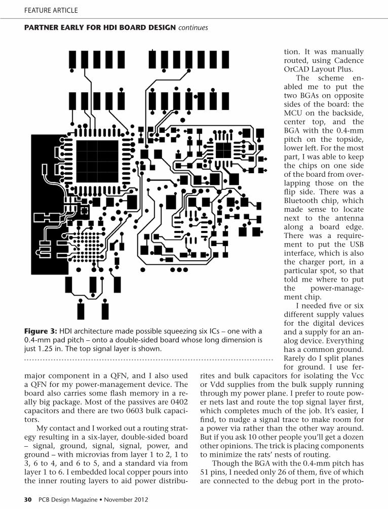
major component in a QFN, and I also used a QFN for my power-management device. The board also carries some flash memory in a re-ally big package. Most of the passives are 0402 capacitors and there are two 0603 bulk capaci-tors.
My contact and I worked out a routing strat-egy resulting in a six-layer, double-sided board – signal, ground, signal, signal, power, and ground – with microvias from layer 1 to 2, 1 to 3, 6 to 4, and 6 to 5, and a standard via from layer 1 to 6. I embedded local copper pours into the inner routing layers to aid power distribu-
tion. It was manually routed, using Cadence OrCAD Layout Plus.
The scheme en-abled me to put the two BGAs on opposite sides of the board: the MCU on the backside, center top, and the BGA with the 0.4-mm pitch on the topside, lower left. For the most part, I was able to keep the chips on one side of the board from over-lapping those on the flip side. There was a Bluetooth chip, which made sense to locate next to the antenna along a board edge. There was a require-ment to put the USB interface, which is also the charger port, in a particular spot, so that told me where to put the power-manage-ment chip.
I needed five or six different supply values for the digital devices and a supply for an an-alog device. Everything has a common ground. Rarely do I split planes for ground. I use fer-
rites and bulk capacitors for isolating the Vcc or Vdd supplies from the bulk supply running through my power plane. I prefer to route pow-er nets last and route the top signal layer first, which completes much of the job. It’s easier, I find, to nudge a signal trace to make room for a power via rather than the other way around. But if you ask 10 other people you’ll get a dozen other opinions. The trick is placing components to minimize the rats’ nests of routing.
Though the BGA with the 0.4-mm pitch has 51 pins, I needed only 26 of them, five of which are connected to the debug port in the proto-
PARTNER EARLY FOR HDI BOARD DESIGN continues
Figure 3: HDi architecture made possible squeezing six iCs – one with a 0.4-mm pad pitch – onto a double-sided board whose long dimension is just 1.25 in. The top signal layer is shown.
Feature article