Embed Size (px)
Citation preview

FROM
NIKHIL KUMAR
NIRT BHOPAL

Initially Circuit Diagram of IC’s are designed…..

Formation Of Wafers from Huge Monocrystal…..
Wafers Cut from Crystal
Wafers pieces

Formation of silicon lattice takes place

Silicon Disk is carried to a Cleaned
Room and 25 of Disks are Packed
in a Sealed Container and Passed
through 100’s of Manufacturing
Steps.
The Photolithographic technique
Transfers Circuit Structures to
Wafers.
Photosensitive resist is applied on
the silicon Disk.

UV lights transfer circuit Structures depicted on
mask to wafers.

Exposed Parts are Removed & these Structures can
be used as Templates…..
Ion Implantation of Wafer’s is done where electrical properties is
specified by using its property of Conductivity…..

Dopants Atoms are injected in silicon atom & is distributed randomly in
lattice.
At high temp. these atoms acquires fixed position.
Random Dopants Atoms

Fixed dopants atoms

Barrier Layer is applied which prevent short Circuit and after that cleaning is
done to remove tiny dust Particles.
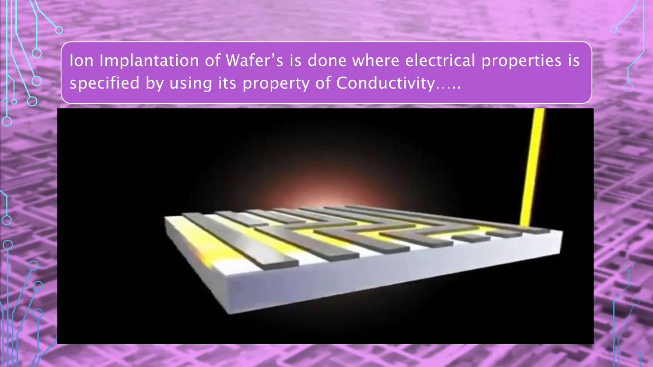
Copper is used to interconnect transistors to form IC’s
Excess copper is Removed and levelled

About two month later, a single wafer is formed which links
up billion of transistors

Lattice structure Appearance…..
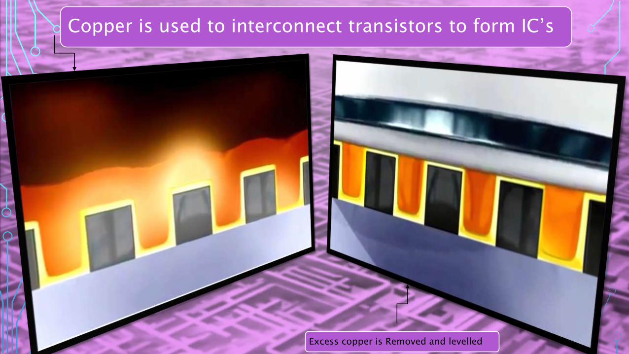
Last Step is Packing of Chip where chip is cut-off from wafers.
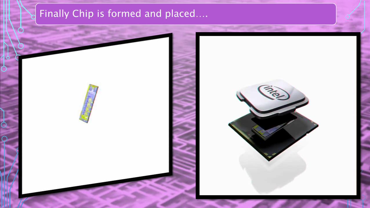
Finally Chip is formed and placed….

THANKS……