Embed Size (px)
DESCRIPTION
Electronic Circuit
Citation preview

Chapter
Useful Electronic Circuits and Construction Techniques
to Get You Going
119
6
6.1 Introduction
So far we have covered some of the theoretical basics involved in making goodoptical laboratory measurements and in the electronic circuitry needed. Weknow a little about sources and detectors, their noise, and the added noise ofamplifiers and about the beauty and power of modulation and synchronousdetection. Circuit diagrams, calculations, and simulations are all very necessary,but whatever measurements you want to do, at some point you must put thetheory into practice and build something! Sure, things will go wrong and notwork as you hoped, so it is important to learn about the limitations and prac-tical problems of electronics and optoelectronics in this environment, debug-ging the problems and figuring out what caused them. In my experience thismeans making lots of circuits, so you don’t want to waste time searching forcircuit fragments to do the job or actually constructing them. In general, thesame needs and problems crop up time and again. Hence it is useful to have acollection, initially just designs but over time a physical collection, of the keycircuits. Source drivers, synchronous detectors, clock oscillators and so on willbe very useful in quickly assembling experiments; it is the flux of these exper-iments, properly evaluated, that generates experience. Later in this chapter wegive a small collection of the “electronic clichés” you will need, together withsome suggestions for actual components. Generally the circuits are rathertrivial, but not if you need to search hours for them or spend time getting themto work.
6.2 Circuit Prototyping and PCBs
There are many different ways to rapidly prototype small circuits. For instance, the hobby catalogs offer “pluggable” circuit boards for through-hole
Source: Photodetection and Measurement
Downloaded from Digital Engineering Library @ McGraw-Hill (www.digitalengineeringlibrary.com)Copyright © 2004 The McGraw-Hill Companies. All rights reserved.
Any use is subject to the Terms of Use as given at the website.

components aimed at this need. With a hundred or so holes arranged in an XY-array in a plastic brick, they have all the X axis rows connected internally. The idea is that you insert the components and bridging wires moreor less in the Y direction, with the X connections taken care of internally. If youuse these, it is important to use solid-core connecting wires to allow easy inser-tion. Stranded wire splays and either won’t go into the holes or goes in andmakes connections you don’t want.
However, the plastic blocks are not usually screened, and the large conduc-tor strips attached to every point in the circuit can make for odd performance.Wrapping aluminum foil around the block and grounding it with an alligatorclip can help, but I have never been very happy with this solution. On manyoccasions I used to forget about the X-direction connections, with disastrousresults. They work better with digital logic ICs than with the variable packagesof analog components.
I have similar small accidents with copper strip board. This is insulatingmaterial with a dense array of punched holes (usually on 0.1-inch centers), andparallel strips of laminated copper foil, protected by a solderable lacquer. Theconnections must be soldered for this. The ideas of using the board to make the X-direction connections, leaving the Y direction for component leads andwire bridges is similar to that of pluggable boards. At least here the hole andcomponent density is high enough to be useful, and once soldered the compo-nents remain connected. You also have the option to sever the copper strips asneeded using a few turns of a handheld drill bit or the tool supplied for the job.It is a big advantage to plan and draw out the circuit completely before start-ing to solder. Even coarse graph paper or a word processor with a fixed char-acter pitch font is suitable for this. As with pluggable boards, I generally forgetto sever a few lines, with results that are at best hard to understand. Reamingout the little copper areas to isolate different regions of copper strip is alsofraught with risk; it’s easy to leave a few microscopic shards of copper to shortout power lines and clamp logic gates to one state. A good inspection under alensed desk lamp or low-magnification stereo microscope is beneficial. Mostlayout problems are visible.
Years ago I used to spend hundreds of hours carefully laying out professionalprinted circuit boards on a CAD system. These had to be photo-plotted on plasticfilm, and then sent for transferring onto copper laminate board for subsequentetching. This took several days but only took a couple of minutes to discoverthat the circuit was seriously flawed. The throughput of this approach can belimiting.
The approach that has lasted best with me is the use of blob board. This issingle-sided, copper-laminated composite board material, just like the stripboards mentioned above, one of the family of Veroboard products. However,instead of copper strips, this one has a predrilled array of isolated square copperpads on 0.1-inch centers. In this case you have to make all the connections your-self. With a small soldering iron, flux-cored solder, and a little practice, it is pos-sible to quickly “draw” circuits in solder onto this blob board, bridging betweenthe copper islands.
120 Chapter Six
Downloaded from Digital Engineering Library @ McGraw-Hill (www.digitalengineeringlibrary.com)Copyright © 2004 The McGraw-Hill Companies. All rights reserved.
Any use is subject to the Terms of Use as given at the website.
Useful Electronic Circuits and Construction Techniques to Get You Going

6.3 Basic Receiver Layout
Let’s look at a simple concrete example, the basic transimpedance amp (Fig.6.1). It is an opamp design using a single 8-pin DIP amplifier package. A dis-crete transimpedance capacitance has been included to roll off the transimped-ance at high frequencies for stability and to reduce gain-peaking. We are usingsymmetrical power rails, although the output will be only positive-going withthe photodiode as drawn. I have included small power rail decoupling capaci-tors (e.g., 100nF) which should be connected as close as possible to the IC. Youmight get away without them, but the 51W resistors help to form a low-passfilter to suppress injected high-frequency noise and feedback through the powerrails. The opamp’s power-supply rejection-ratio is large but not infinite anddegrades with frequency. It is easier if you do it every time. The 51W value ischosen to drop not more than a couple of hundred millivolts at the peak opampsupply current. The resistors also make layout easier as they add an extradegree of topological freedom to cross over other conductors. I try to use thesame lead spacing for all similar component connections, not changing thespacing to fit the design (0.2 inch for the tiniest 1–8 W metal film resistors, 0.4inch for standard 1–4 W resistors, and 0.1 and 0.2 inch for capacitors).
Useful Electronic Circuits and Construction Techniques to Get You Going 121
(b) Top view
+12V
+12V
-12V
-12V
GND
GND
Output
Output
PD
PD
+
-Rf
R1 51+12V
-12V
2
(a)
(c) Underside view (d) Solder
75
43
R2 51
C1C2 0.1µF
C1 0.1µF
Cf
APD1
1
1
R1
R2
Rf
Cf
C2
Figure 6.1 Blob-board construction. A circuit is converted to a square-grid layout showingall components and offboard connections. The underside view allows easy drawing of thecircuit wiring in solder on isolated copper islands.
Downloaded from Digital Engineering Library @ McGraw-Hill (www.digitalengineeringlibrary.com)Copyright © 2004 The McGraw-Hill Companies. All rights reserved.
Any use is subject to the Terms of Use as given at the website.
Useful Electronic Circuits and Construction Techniques to Get You Going

Construction starts with your circuit diagram, making sure that all compo-nents are present, including power supplies, decoupling capacitors, and offboardconnections, and that all IC pin numbers are correct. Draw the components inpencil on coarse graph paper. I prefer something on a grid of about 5 to 6mm.This can be bought through office supply and art shops. If it is a problem tofind, print something equivalent from the PC. Each square represents the 0.1inch of the blob board. It’s not 1 :1, but neither is it a problem to follow frompaper to board. The aim is to lay out the component positions to optimize per-formance. Critical paths such as the feedback network and the photodiode con-nection should be as compact as possible to minimize unwanted pickup. We haveseen how dependent performance can be on a few picofarads of extra capaci-tance here. Component connections are drawn onto the coarse graph paperusing strict north, south, east, west routing. It might take a couple of tries toget a neat layout throughout. With a little luck, the components themselves canprovide most of the flexibility needed, avoiding all but a few wire bridges. Thesecan be of bare tinned copper wire for rectilinear runs on top of the board, orfine solid-core insulated wire for connections underneath. Tefzel or Kynar30AWG (0.25mm) insulated wire-wrap wire is perfect for this, easily strippedwith the right tool and proof against overheating by the soldering iron. For off-board connections you can use 1-mm-diameter pushpins (“Veropins”) made forthese boards, with soldered wire connections. Tiny screw terminals with con-nections on 0.1-inch centers are also available, which work well with blob board.Make sure you use sufficient pushpins to act as test points for all importantsignals and a convenient ground pin or wire-loop for your scope probe ground.Changes and errors are quickly corrected with an eraser. Figure 6.1b shows thedesign layout. On this layer I have the components, wire connections, and allthe labels. This view will be used for debugging.
Once the layout is finished, I make a hand copy onto tracing paper (or mattpolycarbonate drawing sheet) again with a pencil. This is very quickly done,taking only a minute or two. Only the connections are drawn on this layer notthe component bodies. You can avoid one step by drawing straight onto translu-cent graph paper. Art shops sell this too, or you can print your own. The onlyproblem is that the underside view still includes all the component bodies,which is too much information. Hence I prefer the two-sheet approach.
Working from the top view and following the layout, the components are nowinserted into the blob board exactly as in the paper layout. Count squares tomake sure everything looks right. Small placement errors can be trivial or di-sastrous, depending on the local topology. Clamp the components with a clothor soft sponge, flip the board over, and solder the leads into place. Just one con-nection per component will do. A soldering iron with a round 1.5-mm-diametertip is about right, allowing one pad to be heated without touching its neighbor.Check that everything is held in place, and correct any components that arefalling out of the board or leaning over. Complete all the component solderingand cut excess component leads flush with the solder bumps using sharp side-cutters. Now the “wiring” can begin.
122 Chapter Six
Downloaded from Digital Engineering Library @ McGraw-Hill (www.digitalengineeringlibrary.com)Copyright © 2004 The McGraw-Hill Companies. All rights reserved.
Any use is subject to the Terms of Use as given at the website.
Useful Electronic Circuits and Construction Techniques to Get You Going

Turn the board and the tracing layout over to view the underside (Fig. 6.1c,d).The components will still be obvious by comparison with the traced view, if ithasn’t been weeks since you made the layout. Following the traced wiring, younow need to “draw” the wiring with solder. This is a rapid process. The boardshould be held firmly in a small vice or clamp, as you will need to apply somepressure from the soldering iron to get fast, thermally conductive connectionsto the pads. A small rotational oscillation of the iron in your fingers scrubs thetip against the pad and greatly improves heat transfer. First put a solder blobonto each square pad along the wiring route, using a touch of the hot iron andthen a couple of millimeters of flux-cored solder. Once all the solder bumps arein place, they can be joined together. This involves melting the second bump ina row, dragging the molten solder over the insulating gap back to the first solidbump, adding a small additional amount of fluxed solder, and then quicklyremoving the iron. If this is judged correctly, the molten blob will melt into theprevious solid blob, form a good connection, and promptly solidify. Solid solderwill then have bridged the gap, and the second and third blobs can be joined inthe same way. If too much heat is applied, usually by performing the backwardsweep too slowly, both blobs will melt and the high surface tension will sepa-rate the solder into two unconnected islands. Immediately trying again willoften frustratingly just add to the size of the two molten blobs, because the tem-perature of the whole area is now too high. If this happens blow on the boardor wait ten seconds for everything to cool down and try again. This is all easierto do than to describe, although it does take a little practice. Figure 6.1d showsthe final result.
Once you have the touch, this drawing in solder process can be very efficientand extremely fast and rarely results in misconnected circuits. You have, afterall, sorted out all the topology beforehand on paper. Nevertheless, a final checkof the physical board against the underside paper view is recommended, againusing the magnifier or stereo microscope.
When all wiring is complete, you will have used a lot of solder, so much of thecircuit will be covered in excess flux; this must be removed. The commercialaqueous flux cleaners are ideal for this. Immerse the whole board in the cleanerfor five minutes, and then scrub the board underside with an old toothbrush.Finally, rinse the board under running tap water until all trace of a soapy feelhas gone. If you have any, rinse also in deionized water, dry the board on labo-ratory paper or a paper towel, and then place in a warm airing cupboard orunder a tepid hair dryer to dry. As we discussed in Chap. 3 failure to removethe flux can lead to odd performance in detector circuits, due to its significantconductivity. A few components, notably some piezo sounders, batteries,switches, and unsealed relays, should not be immersed. They will be added afterwashing and drying.
The act of laying out on paper helps to make the layout perfect, so that Irarely need to make any corrections. Gross errors can be corrected using copperbraid or a “solder-sucker” to aspirate solder along a line of connection bumps.These work very well on the single-sided, nonplated hole boards. Similarly,
Useful Electronic Circuits and Construction Techniques to Get You Going 123
Downloaded from Digital Engineering Library @ McGraw-Hill (www.digitalengineeringlibrary.com)Copyright © 2004 The McGraw-Hill Companies. All rights reserved.
Any use is subject to the Terms of Use as given at the website.
Useful Electronic Circuits and Construction Techniques to Get You Going

components can be exchanged by sucking up excess solder around the leads andpulling out the component. If extensive modification needs to be done in sensi-tive areas, such as around the inputs and feedback resistors in transimpedanceamplifiers, flux cleaning may need to be done again. If you change the layout,change the paper drawing to match. If you need to review the design in thefuture it should correspond with what you see.
The main advantage of this well-practiced approach is its speed. Small cir-cuits can be drawn, laid out, and soldered in an hour or two. If you keep col-lections of designs for preexisting transimpedance amplifiers, synchronousdetectors, modulators, power supplies, filters, etc., they can be easily reusedwith very little new layout work. With simple circuits you may have a suffi-ciently good mental picture of the mirror-image underside view to avoid thetransparent paper step. The only remaining task is to file away your design sothat it can be reused in the future and perhaps to label the board’s externalconnections. A word processor set to print small labels in 4- or 6-point type forgluing onto the board is about right. A digital photograph of the board can bevery useful; scan the completed board, top view and underside, on an officeflatbed color scanner. The depth of field is usually adequate.
If you need a couple of identical simple boards, the blob board method is stillthe best approach. Once you need more, and the performance has already beenverified, this approach represents too much work and a conventional PCB isprobably a better approach. Once the graph paper layout has been designed andtested, it is usually straightforward to transfer to a PCB layout. Almost all ofthe layout thinking and optimization has been done already. The main differ-ence is that the blob board doesn’t allow tracks to be placed between IC pins,so the PCB can be a little denser.
6.4 LED Drive and Modulation
It may seem a little trivial to discuss how to drive an LED, but it is not uncom-mon for users to treat them like a lightbulb, connect them to a battery, beimpressed at how bright they are, but disappointed in their short lifetime! Theproblem is that they are diodes, and Shockley said that the current flowingthrough them varies roughly exponentially with the voltage across them. Hencealthough you can drive them from a low-impedance voltage source such as aDC power supply, even small increases in supply voltage will lead to large andpossibly destructive increases in current. It is therefore much more pleasant touse a higher-impedance source that defines the current and allows the diodevoltage take on whatever value it needs.
To use the LED you need to know the maximum forward current that it canbear (typically 20mA for a common visible LED, perhaps 200mA for a high-power infrared device) and the maximum reverse voltage it can handle withoutbreaking down and passing damaging currents (typically only a few volts). Youget these figures from the data sheet. Then we can choose the voltage sourceVb and series resistor. There is a lot of leeway. A low voltage and small resistor
124 Chapter Six
Downloaded from Digital Engineering Library @ McGraw-Hill (www.digitalengineeringlibrary.com)Copyright © 2004 The McGraw-Hill Companies. All rights reserved.
Any use is subject to the Terms of Use as given at the website.
Useful Electronic Circuits and Construction Techniques to Get You Going

works as well as a high voltage and a high resistor. However, the higher thevoltage, the more like a pure current source it looks and the more stable willbe the current with temperature variations in the LED. In Fig. 6.2a the currentI = (Vb - Vf)/R. Unfortunately, the diode voltage Vf is also a function of current,but not much of one, just logarithmic. Hence a reasonable approach, since youprobably don’t know the details of the IV characteristic of the cheap LED, is totake any available 5V or 12V DC supply or battery, assume a forward LEDvoltage of 1.5V, an operating current of 10mA and calculate the load resistor.Power it up, measure the LED voltage, and adjust the resistor if necessary. It’sunlikely that you will be far wrong. If the LED is more costly or you don’t havea replacement, you might start with a ten times larger resistor or wind up thesupply voltage slowly, monitoring the current until you are sure of the polarity,the characteristics, and hence the necessary design.
Connecting to a laboratory signal generator to modulate the LED is hardlyany more complex (Fig. 6.2b). Use the peak generator voltage instead of Vb inyour calculations and proceed as above. Unless the LED has a metal can whichyou would like to ground, you might want to swap the positions of LED andload resistor as shown. This makes it easier to monitor the LED current via thevoltage on the load using a grounded oscilloscope. If the generator is bipolar,one half-cycle could take the LED into breakdown. If you suspect this, limit the
Useful Electronic Circuits and Construction Techniques to Get You Going 125
Vb(12V)
Vb(9V)
LED
V+
V-
100R
Rset6.8R 2.2k
10k 10k
470
2N2222 VN2222
470
12V12V
LM334(bottom view)
5–30V
820R
2N2906
RedLED
Vb(12V)
1kC±5V
330RVf (1.6V)
R (560)
±5V
(a)
(d) (e) (f) (g)
(b) (c)
Si
LED
R (180)I (18.6mA)
S
DG
Figure 6.2 LED drive circuit fragments. As the LED is a diode, it is more comfortable to definethe LED current and let the voltage take on whatever value it needs. (b) and (c) show square wave and sine wave modulation schemes. (d), (e) are simple DC current generators. If more current is needed than an opamp or CMOS logic gate can supply, use a bipolar transistor or FETbuffer (f,g).
Downloaded from Digital Engineering Library @ McGraw-Hill (www.digitalengineeringlibrary.com)Copyright © 2004 The McGraw-Hill Companies. All rights reserved.
Any use is subject to the Terms of Use as given at the website.
Useful Electronic Circuits and Construction Techniques to Get You Going

LED reverse current or voltage by connecting a silicon diode either in series orin reverse parallel, respectively. The load resistor should always be large enoughto avoid exceeding the current output capability of the generator.
This works fine with square-wave generators and on/off LED output. If youwant instead to sine-wave modulate the output, you will need to bias the LEDwith a DC current first. One way is to use a DC supply and resistor to give abouthalf the maximum allowed LED forward current, and AC couple the bipolarsine-wave generator to the LED, as shown in Fig. 6.2c. The AC generator canthen add its current up to the LED maximum and reduce it to zero. As before,make sure the generator can drive the series resistor load without damage. Thecapacitive coupling and series resistor lead to a high-pass characteristic, so Chas to be large enough not to attenuate the frequency you want to use. ChooseRC >> 1/fmod and use a nonpolarized capacitor. Using a little care in setting upthe other components, the capacitor can be dispensed with altogether. To setup the modulation amplitude, observe the LED output on your receiver. Toomuch modulation current or too little bias will lead to a clipped sine-waveoutput.
If you use a lot of LEDs, in routine testing it is useful to have an active currentgenerator set up for about 10mA. This can be a single-transistor circuit as inFig. 6.2d. The red LED acts as an indicator and also provides a relatively con-stant voltage of about 1.6V to the transistor base. The base-emitter junctionloses another 0.6V, to give 1V across the emitter resistor. One volt and 100W is10mA, which also flows through the collector and LED. Whatever the LED andeven if the LED terminals are shorted together, the current remains near to10mA, so the circuit is quite robust. Last, there are even simpler integratedcircuit current generators available such as the LM334 (Fig. 6.2e). This is a high-precision current regulator that can deliver up to about 10mA. Both Figs. 6.2dand e only need a small battery with 6V or 9V for long-life operation.
When you want to drive the LED from low power circuitry, including opampsand CMOS logic, their current capability may be a bit marginal. In that caseuse a bipolar or FET transistor used as a switch, as in Figs. 6.2f and g. Anysmall npn-transistor will be fine, such as a BC548, 2N3904 or ZTX450. You caneven avoid wiring the two resistors by choosing the new “digital transistors”.Infineon does a good range, such as the BCR108, BCR112 which can sink100mA. Rohm’s range (e.g., DTC114EKA) is very similar. These are surface-mount devices. Arrays of small switching transistors in a single package arealso convenient. Intersil’s CA3081E contains seven common-emitter npn-transistors in a DIP16 package. For the FET any small n-channel enhancement-mode MOSFET with gate threshold voltage less than about 3V is convenient.The VN2222LL is widely available, and for higher currents Zetex does a goodrange such as the ZVN2106A series. These have a channel on-resistance lessthan 2W and can handle 450mA continuously. As they are operated as switches,both drivers need a series resistor to limit LED current.
It is not always necessary to drive the LED at or below its nominal current.The main limitations to drive come from temperature rise of the LED chip,
126 Chapter Six
Downloaded from Digital Engineering Library @ McGraw-Hill (www.digitalengineeringlibrary.com)Copyright © 2004 The McGraw-Hill Companies. All rights reserved.
Any use is subject to the Terms of Use as given at the website.
Useful Electronic Circuits and Construction Techniques to Get You Going
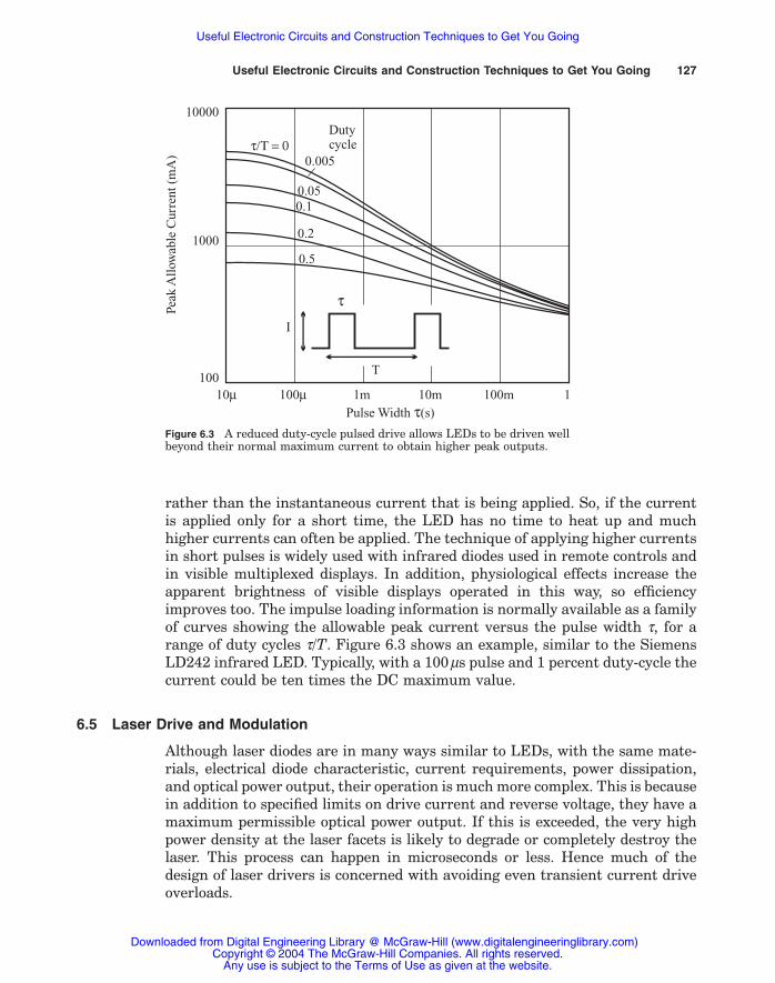
rather than the instantaneous current that is being applied. So, if the currentis applied only for a short time, the LED has no time to heat up and muchhigher currents can often be applied. The technique of applying higher currentsin short pulses is widely used with infrared diodes used in remote controls andin visible multiplexed displays. In addition, physiological effects increase theapparent brightness of visible displays operated in this way, so efficiencyimproves too. The impulse loading information is normally available as a familyof curves showing the allowable peak current versus the pulse width t, for arange of duty cycles t/T. Figure 6.3 shows an example, similar to the SiemensLD242 infrared LED. Typically, with a 100ms pulse and 1 percent duty-cycle thecurrent could be ten times the DC maximum value.
6.5 Laser Drive and Modulation
Although laser diodes are in many ways similar to LEDs, with the same mate-rials, electrical diode characteristic, current requirements, power dissipation,and optical power output, their operation is much more complex. This is becausein addition to specified limits on drive current and reverse voltage, they have amaximum permissible optical power output. If this is exceeded, the very highpower density at the laser facets is likely to degrade or completely destroy thelaser. This process can happen in microseconds or less. Hence much of thedesign of laser drivers is concerned with avoiding even transient current driveoverloads.
Useful Electronic Circuits and Construction Techniques to Get You Going 127
10m 100m 1m 10m 100m100
0.5
0.2
0.10.05
0.005
1000
10000Dutycycle
1Pulse Width (s)
T
I
t
t
t/T = 0
Peak
All
owab
le C
urre
nt (
mA
)
Figure 6.3 A reduced duty-cycle pulsed drive allows LEDs to be driven wellbeyond their normal maximum current to obtain higher peak outputs.
Downloaded from Digital Engineering Library @ McGraw-Hill (www.digitalengineeringlibrary.com)Copyright © 2004 The McGraw-Hill Companies. All rights reserved.
Any use is subject to the Terms of Use as given at the website.
Useful Electronic Circuits and Construction Techniques to Get You Going

They also exhibit a strong nonlinear output/current characteristic, in whichan increase in drive current initially produces little light output, but above acertain threshold current the output increases rapidly (Fig. 6.4). Even simplebiasing is difficult, and it is not advisable to just connect to a variable currentsource and hope for the best, as with an LED. For example the drive current“Bias 1” in Fig. 6.4 may initially give the desired output, here about 0.75mW.However, as soon as the laser is powered up, it also warms up, which can shiftthe threshold characteristic to the higher current characteristic shown. Thismay completely switch off the laser output by taking it below threshold. If thecurrent is instead raised a few milliamps to give the increased output (Bias 2)at the higher operating temperature, and the ambient temperature drops a fewdegrees, the output power may easily climb to a value exceeding the specifiedoptical power limit, causing degradation or damage. These characteristics arecontained in the IV (current-voltage) and PI (optical power output-current)characteristic curves, which are supplied with the laser diodes, either individ-ually or as family characteristics.
To deal with this problem of output power control, the great majority of low-power laser diode packages have three pins, connected to the laser itself andalso to a monitor diode picking up light from the laser’s rear facet. The pho-tocurrent from this monitor diode varies approximately linearly with the laser’sfront facet output, and it is this signal that must be controlled to limit outputpower overloads. The high collection efficiency and hence high photocurrent
128 Chapter Six
Low
-T
Optical Power Limit Hig
h-T
Thresholdcurrents
Bia
s 2
Max
. Cur
rent
Lim
it
Bia
s 1
00.0
1.0
1.5
2.5
0.5
2.0
3.0
25 50 75 100Drive Current (mA)
Sin
gle
Face
t Out
put P
ower
(m
W)
Figure 6.4 Laser diodes exhibit a threshold characteristic.Normally we bias just above threshold and modulate withcurrent pulses above. There are both maximum current andmaximum power limits for each device and the thresholdcurrent, in particular, is temperature dependent. Correctbiasing is simplest with feedback control from a monitor pho-todiode.
Downloaded from Digital Engineering Library @ McGraw-Hill (www.digitalengineeringlibrary.com)Copyright © 2004 The McGraw-Hill Companies. All rights reserved.
Any use is subject to the Terms of Use as given at the website.
Useful Electronic Circuits and Construction Techniques to Get You Going

detected means that sensitivity is not a problem (typically it is 100mA or more).The design with a common pin means that you will find four different connec-tion permutations of commoned electrodes, which must be handled differently(Fig. 6.5). The “parallel” configurations in Figs. 6.5c and d are less convenientas they ideally need bipolar power supplies to power the laser and to extractthe reverse-biased photodiode’s photocurrent. The “antiparallel” configurationsin Figs. 6.5a and b are easy to use with a single supply.
Typical electronic power control circuitry uses a feedback control system. Asit is so important to avoid even short overshoot spikes, the controllers are usuallyset up as heavily damped PI (proportional, integral) types. These drive the laser with a signal that is the integral of the difference (error) between the set point and the actual photocurrent values. Figure 6.6 shows one possibilityfor the antiparallel form. The laser is driven from a high-impedance single-
Useful Electronic Circuits and Construction Techniques to Get You Going 129
Ip
Ip
Ip
Ip
+ve(a)
(c)
(b)
(d)
Gnd Gnd
GndGnd
-ve
-ve +ve
+ve -ve
+ve -ve
Ilaser
Ilaser
Ilaser
Ilaser
Figure 6.5 All four permutations of laser and monitorphotodiode polarity are available. The “antiparallel”configurations are slightly more convenient to use witha single-polarity power supply.
+
-
Laser
1µFIp
1.24V Ref.ZRA124Y
3.9k
V +
V-2.2k
47 100µF
10k
100nF
Set-point
Damping10µF
Rail-railopamp Current source
2N2905
PD
+5V
Figure 6.6 Example of a DC laser power-stabilization circuit.
Downloaded from Digital Engineering Library @ McGraw-Hill (www.digitalengineeringlibrary.com)Copyright © 2004 The McGraw-Hill Companies. All rights reserved.
Any use is subject to the Terms of Use as given at the website.
Useful Electronic Circuits and Construction Techniques to Get You Going
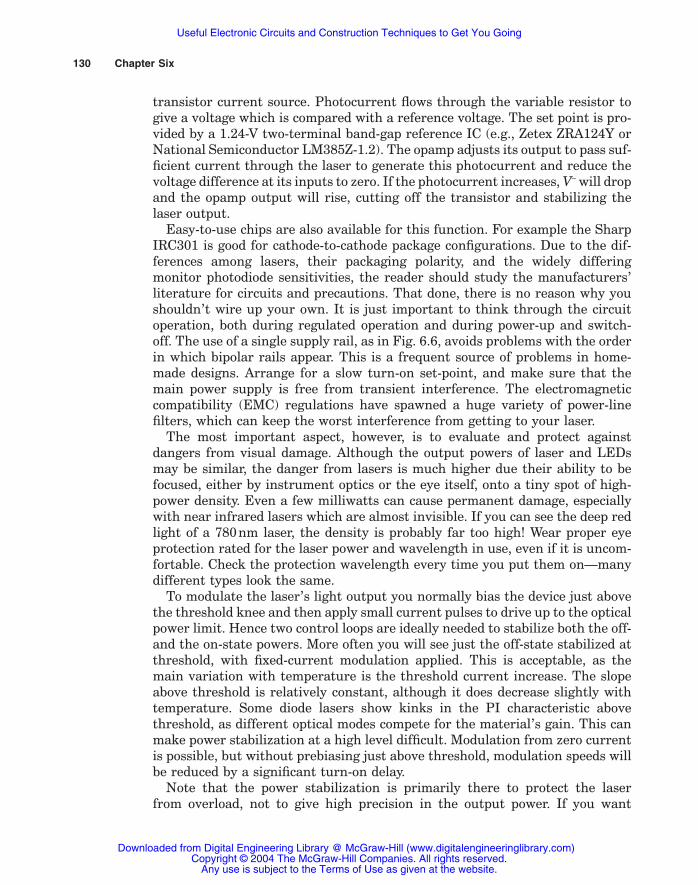
transistor current source. Photocurrent flows through the variable resistor togive a voltage which is compared with a reference voltage. The set point is pro-vided by a 1.24-V two-terminal band-gap reference IC (e.g., Zetex ZRA124Y orNational Semiconductor LM385Z-1.2). The opamp adjusts its output to pass suf-ficient current through the laser to generate this photocurrent and reduce thevoltage difference at its inputs to zero. If the photocurrent increases, V- will dropand the opamp output will rise, cutting off the transistor and stabilizing thelaser output.
Easy-to-use chips are also available for this function. For example the SharpIRC301 is good for cathode-to-cathode package configurations. Due to the dif-ferences among lasers, their packaging polarity, and the widely differingmonitor photodiode sensitivities, the reader should study the manufacturers’literature for circuits and precautions. That done, there is no reason why youshouldn’t wire up your own. It is just important to think through the circuitoperation, both during regulated operation and during power-up and switch-off. The use of a single supply rail, as in Fig. 6.6, avoids problems with the orderin which bipolar rails appear. This is a frequent source of problems in home-made designs. Arrange for a slow turn-on set-point, and make sure that themain power supply is free from transient interference. The electromagneticcompatibility (EMC) regulations have spawned a huge variety of power-linefilters, which can keep the worst interference from getting to your laser.
The most important aspect, however, is to evaluate and protect againstdangers from visual damage. Although the output powers of laser and LEDsmay be similar, the danger from lasers is much higher due their ability to befocused, either by instrument optics or the eye itself, onto a tiny spot of high-power density. Even a few milliwatts can cause permanent damage, especiallywith near infrared lasers which are almost invisible. If you can see the deep redlight of a 780nm laser, the density is probably far too high! Wear proper eyeprotection rated for the laser power and wavelength in use, even if it is uncom-fortable. Check the protection wavelength every time you put them on—manydifferent types look the same.
To modulate the laser’s light output you normally bias the device just abovethe threshold knee and then apply small current pulses to drive up to the opticalpower limit. Hence two control loops are ideally needed to stabilize both the off-and the on-state powers. More often you will see just the off-state stabilized atthreshold, with fixed-current modulation applied. This is acceptable, as themain variation with temperature is the threshold current increase. The slopeabove threshold is relatively constant, although it does decrease slightly withtemperature. Some diode lasers show kinks in the PI characteristic abovethreshold, as different optical modes compete for the material’s gain. This canmake power stabilization at a high level difficult. Modulation from zero currentis possible, but without prebiasing just above threshold, modulation speeds willbe reduced by a significant turn-on delay.
Note that the power stabilization is primarily there to protect the laser from overload, not to give high precision in the output power. If you want
130 Chapter Six
Downloaded from Digital Engineering Library @ McGraw-Hill (www.digitalengineeringlibrary.com)Copyright © 2004 The McGraw-Hill Companies. All rights reserved.
Any use is subject to the Terms of Use as given at the website.
Useful Electronic Circuits and Construction Techniques to Get You Going

high intensity measurement precision with a diode laser source, more care willbe needed. Instead of using the laser’s rear facet detector for stabilization, youcould use the front facet output, for example using a small beam-splitter, andthereby remove one source of error. In practice it is easier to use the internalrear-facet detector for rough intensity stabilization, with an external precisiondetector for referencing. Note too that the laser stabilization circuits are justas applicable to light emitting diodes, given an independent detector. Tech-niques for power stabilization and referencing are described in Chap. 8.
6.6 Modulation Oscillators
In the great majority of optical measurement systems the light source will bemodulated, and for LED-sourced systems the basic requirements are, well,basic. There is nothing very wrong with using the “555” timer IC in its astablemultivibrator mode (Fig. 6.7). The simple circuit does not allow equal on andoff times, but this can be remedied by moving RB to the pin 7 connection, as onthe right side of the figure, and restricting it to no greater than 1/2RA. Other-wise threshold will not be reached and the circuit will not oscillate. See theNational Semiconductor Corp. data-books and application notes for details.They are all on the web site, but the printed information is more educational.This IC, one of the most successful and widely used of all time, is available ina variety of technologies. The original LM555 bipolar devices offered a power-ful 200mA source and sink capability. This is sufficient to directly power manyhigh-current LEDs. Newer CMOS versions are available with operating voltagedown to 1V, much lower input and quiescent currents, and greatly reduced“crowbar” current spikes during the timer reset period. A better way to obtainaccurate 50 :50 mark-to-space (M/S) ratio square waves for synchronous detec-tion use is to operate the oscillator depicted in Fig. 6.7 at double frequency anddivide by two in a D-type flip-flop as below. This ensures accurate M/S even withhighly asymmetric input waveforms.
Useful Electronic Circuits and Construction Techniques to Get You Going 131
1
3
RA RA=51k
Vss (e.g., 12V) Vss
LED
470
0.1||1.0µF
t1=0.693 (RA+RB)Ct1=0.693 RACt2=0.693 RB C
RBRB=22k
C C=10nF
10nF
6 6
5
2 7 74 8
'555
Figure 6.7 Modulation oscillators using the well-known 555 oscillatorsare common in optical circuitry. The right side shows one way to obtain1 :1 mark-to-space ratio drive.
Downloaded from Digital Engineering Library @ McGraw-Hill (www.digitalengineeringlibrary.com)Copyright © 2004 The McGraw-Hill Companies. All rights reserved.
Any use is subject to the Terms of Use as given at the website.
Useful Electronic Circuits and Construction Techniques to Get You Going

The 555 oscillator can achieve a temperature drift of less than 150ppm/°C,although typical capacitors will drift faster and degrade this figure. We saw inChap. 5, however, that it is often helpful to be able to define the source modu-lation frequency with better precision than this. For example, to avoid the har-monics of fluorescent light interference we might want to set the frequencycarefully between 4000Hz and 4050Hz and have it stay there with tempera-ture changes. Or we might want two oscillators with very similar frequenciesto operate a reference-free synchronous detection configuration. Even innoncritical applications, it is useful to know precisely what the modulation fre-quency is. In all these cases it will be easier to use a precision resonator oscil-lator, rather than an RC-oscillator design.
The cheapest route to initial frequency accuracy and temperature stability(typically ±20ppm/°C) is the 32.768-kHz crystal used in most clocks andwatches. These are available in several through-hole and surface-mount pack-ages, including tiny 2mm ¥ 7mm long cylinders. The most common way toexcite all resonators is to connect them as a feedback element around a digitallogic gate. Almost any inverting gate will do. This is the internal design of theHarris HA7210 used in Fig. 6.8, which has some other refinements to optimizeperformance. For example, current drain with the device is very low (ª5mA) and
132 Chapter Six
S
DG
32kHz
32kHz
HA7210
HA7210
8kHz I
16kHz32kHz
8kHz Q
8kHz
VN2222LL
LED12V
220
10k
74HC74
74HC74
5V
5V100nF
100nF
5
5
2
2
1
1
7
7
8
8
9
9
14
14
10k 1,4,10,13
10k 1,4,10,13
3
3
6
6
(b) Two-phase clock
(a) Divided Clock
Q
Q
Q
Q
Q
Q
Q
Q
C
C
C
C
D
D
D
D
11
11
12
12
Figure 6.8 A better way to get 1 :1 mark-to-space ratio drive is togenerate any waveform and then divide by two with a D-type flip-flop (a). The 74HC74 series has two such elements per package,leading to compact and useful modulated sources. A different con-nection (b) gives division but also “quadrature” outputs.
Downloaded from Digital Engineering Library @ McGraw-Hill (www.digitalengineeringlibrary.com)Copyright © 2004 The McGraw-Hill Companies. All rights reserved.
Any use is subject to the Terms of Use as given at the website.
Useful Electronic Circuits and Construction Techniques to Get You Going

includes switchable elements to optimize internal circuitry for low-frequencyclock crystals or higher frequency resonators. No extra components are neededexcept for power supply decoupling, placed as close as possible to the chip. Theonly potential difficulty with this chip is the very high impedance at which theinputs work. Even low levels of leakage around the crystal connection pins willstop the circuit oscillating. This includes PCB leakage currents, so it is impor-tant that the board is carefully cleaned of flux residues and preferably guardedas recommended in the application guidelines. If the 32kHz output is too fastfor the application, division stages can easily be added in CMOS D-type logic asshown. The 74HC74 contains two dividers, getting you down to 8kHz. The samecomponents, connected differently, can provide 90° phase shifted outputs I andQ. Using CMOS logic, this module will operate any conventional LED using asingle 3.3V lithium cell and an FET or transistor buffer. Another useful IC isthe 74HC4060, which combines a free inverting gate between pins 10 and 11which can be used as an oscillator, and 14 stages of division, with most of thedivision stages made available on pins (Fig. 6.9). With some tweaking of thebiasing components, this will work with a great variety of two-terminal res-onators. The divider chain will get a 32kHz clock crystal down to 2Hz.
Ceramic resonators offer another approach to timing. For example, 455kHzresonators are available from Murata and others, which are economical andeasy to drive. The HA7210 can again be used, or you can make your own circuitusing simple gates. The Murata design notes are very helpful, and recommenda particular kind of logic gate. This is the CD4069UB series (Fig. 6.10). Thesegates are “unbuffered,” which gives a reduced open loop gain compared withbuffered gates, reducing the likelihood of oscillation at a harmonic of the design oscillation frequency. Sometimes it can be difficult to get any of these
Useful Electronic Circuits and Construction Techniques to Get You Going 133
GND
Vcc
Out
128
16 In
32
CLK
64
RST
Crystalresonator,etc.
10M
100nF
74HC4060CD4060
+5V
2x15pF
220k
1616384
512
8192
256
4096
1024
Figure 6.9 The 74HC7060 provides a free gate forexciting crystal resonators, together with a longdivider chain for selection of lower frequencies.
Downloaded from Digital Engineering Library @ McGraw-Hill (www.digitalengineeringlibrary.com)Copyright © 2004 The McGraw-Hill Companies. All rights reserved.
Any use is subject to the Terms of Use as given at the website.
Useful Electronic Circuits and Construction Techniques to Get You Going

piezomechanical resonators to oscillate. This is down to the two loading capac-itors C1, C2 shown in Fig. 6.10. With a good model of the resonator, they can becalculated and chosen analytically. In practice we are often reduced to tweak-ing to get them to work. Luckily, once tweaked, the design is usually transfer-able to other similar devices. Division of the fundamental frequency can simplybe carried out in a divider chain, such as the 74HC4060 already mentioned orthe related HC4020, HC4024, or HC4040.
Neither ceramic oscillators used for radio intermediate frequency filtering northe watch crystal offer sufficient choice of frequencies for some applications. Inthis case, it is convenient to move to the 1 to 10MHz region, where the choiceof conventional quartz crystals is at its best. With correct choice of the loadingcapacitors, all the above circuits can be used. The HC4060 is a nice solution asit includes both the free gate to build an oscillator and a long divider chain toget down to the audio range. If you need even more flexibility, look at the fre-quency synthesizer chips.
134 Chapter Six
Rf =1M
Rd
C1 C2
X-Reson.
CD4069UB
GND
GNDGND
Vcc
Vcc
Vcc
2
2NC
8
12832
4
1616
16
3264
CLK
CLK
CLK
In
In
In
CLK
128
64128
RST
RSTNC
8
HC4040
HC4020HC4024
32
16384RST
512
5124
64
8192
256
2562
4096
4096
1024
1024NC
2048
2048
Figure 6.10 Ceramic resonators are best excited using “unbuffered” logicgates. You may need to tweak the capacitors to get it to oscillate reliably.Alternative divider ICs are also shown.
Downloaded from Digital Engineering Library @ McGraw-Hill (www.digitalengineeringlibrary.com)Copyright © 2004 The McGraw-Hill Companies. All rights reserved.
Any use is subject to the Terms of Use as given at the website.
Useful Electronic Circuits and Construction Techniques to Get You Going
Second only to the bias box in its continuous usefulness around the lab is amodulated LED source. The crystal-controlled audio-frequency transmitter(Fig. 6.8a) with a 3.6V lithium battery is about right for finding out whetheryour receiver has just died, checking the continuity of a fiber link, or testingthe rise time of a new high-sensitivity detector circuit. The circuit is compactenough to be built into a flashlight housing or small diecast box. My recom-mendation is to make several and always keep a few hidden away, as they have a high diffusion coefficient! A good runner-up for testing receivers is a handheld IR remote control. As every TV, video, stereo, gas-fire, and air-conditioning system these days seems to have a remote control and they lastlonger than the equipment itself, there are usually surplus units available. Thewavelength is typically 880nm or 940nm, although changing the LED for a dif-ferent wavelength is not difficult. The slow code transmission can make scopetriggering difficult.
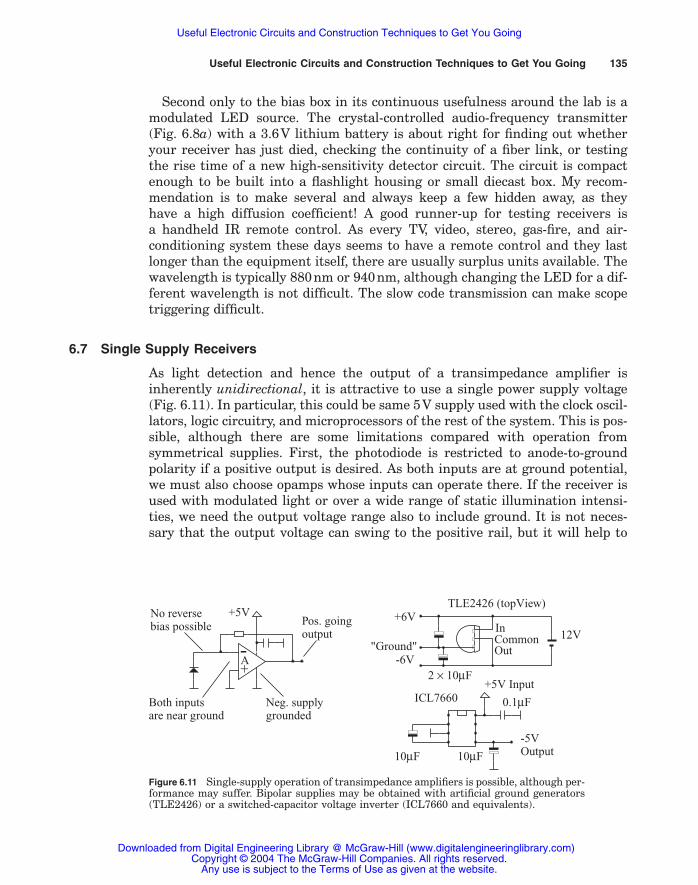
6.7 Single Supply Receivers
As light detection and hence the output of a transimpedance amplifier is inherently unidirectional, it is attractive to use a single power supply voltage(Fig. 6.11). In particular, this could be same 5V supply used with the clock oscil-lators, logic circuitry, and microprocessors of the rest of the system. This is pos-sible, although there are some limitations compared with operation fromsymmetrical supplies. First, the photodiode is restricted to anode-to-groundpolarity if a positive output is desired. As both inputs are at ground potential,we must also choose opamps whose inputs can operate there. If the receiver isused with modulated light or over a wide range of static illumination intensi-ties, we need the output voltage range also to include ground. It is not neces-sary that the output voltage can swing to the positive rail, but it will help to
Useful Electronic Circuits and Construction Techniques to Get You Going 135
ICL7660
TLE2426 (topView)
In12V
+6V
-6V"Ground" Out
Common
+5V Input
0.1µF
10µF 10µF
2 ¥ 10µF
-5VOutput
+
-+5V
Both inputsare near ground
Neg. supplygrounded
Pos. goingoutput
No reversebias possible
A
Figure 6.11 Single-supply operation of transimpedance amplifiers is possible, although per-formance may suffer. Bipolar supplies may be obtained with artificial ground generators(TLE2426) or a switched-capacitor voltage inverter (ICL7660 and equivalents).
Downloaded from Digital Engineering Library @ McGraw-Hill (www.digitalengineeringlibrary.com)Copyright © 2004 The McGraw-Hill Companies. All rights reserved.
Any use is subject to the Terms of Use as given at the website.
Useful Electronic Circuits and Construction Techniques to Get You Going

give the best dynamic range. In a conventional opamp design the output voltageis limited to not closer than about 1.2V (two diode-drops) from the positive rail,and this can be a big loss with a 3.3 or 5V supply. Luckily, you aren’t on yourown in needing these characteristics; almost the whole electronics industry,driven by applications in mobile phones, digital cameras, personal digital assis-tants, MP3 music players, and notebook personal computers is pressing for newopamp designs that stress low-voltage, low-power, rail-to-rail inputs and outputsand operation from the same 3.3 or 5V supply used for the digital circuitry.Hence there is a reasonable and rapidly expanding choice. The downside is thatthese requirements make design for high speed, low offset voltage, good outputdrive capability, etc. much more difficult. In transimpedance configuration somerail-to-rail opamps show severe distortion and instability with low output volt-ages. As your laboratory design is unlikely to be built or abandoned dependingon the cost of a couple of chips, it is often worth just using split supplies, gen-erating split supplies using a specially designed voltage regulator, or generat-ing a low-current negative supply from the +5V rail using an ICL7660 inverter.Figure 6.11 shows a few possibilities. These can be used to supply either thewhole opamp or just the photodiode’s reverse bias. Note that the oscillation fre-quency of the standard devices is fixed in the audio band and can give a lot ofin-band interference which is difficult to screen perfectly. Alternative devicesoffer either much higher operating frequencies or adjustable frequencies, whichcan help to avoid the biggest problems.
6.8 Use of Audio Outputs
In many of the simple systems discussed we have modulated the source in theaudio range, above the region of worst industrial noise, say 500Hz to 20kHz.Because of this, a receiver with an audible output is a very useful piece of equip-ment for optical system testing. This can be used to find out whether the trans-mitter LED is being modulated, or even if the invisible infrared LED is actuallystill alive. In debugging field installations, it may save lots of time and face. Inmultifrequency systems the human spectrum analyzer can even differentiatebetween sources and allows extremely effective detection in the presence ofnoise. You can of course make up a complete battery-powered transimpedancereceiver, small audio amplifier chip such as the LM386, and a speaker or ear-phone. This is the proper approach for testing weak signals. However, even atrivial receiver can be useful.
6.8.1 TRY IT! Minimalist audio photo-receiver
A large area photodiode or small solar cell connected to a pair of headphones, per-sonal audio player earphone, or even a piezobuzzer does a great job. Ideally you wouldlike the most sensitive device you can find. Try to find an old high-impedance ear-phone; 600W or 2kW are best, but even a modern 16W personal stereo earpiece works,albeit with lower sensitivity. Just connect it to a silicon photodiode. An eco-nomical BPW34 is fine, but so is almost anything else. I am lucky to have a twenty-
136 Chapter Six
Downloaded from Digital Engineering Library @ McGraw-Hill (www.digitalengineeringlibrary.com)Copyright © 2004 The McGraw-Hill Companies. All rights reserved.
Any use is subject to the Terms of Use as given at the website.
Useful Electronic Circuits and Construction Techniques to Get You Going

year-old pair of high quality Sennheiser stereo headphones. These have an impedanceof 2kW each, so in series they work very well. Listen close-up to a few modulatedoptical sources: the PC monitor, TV screen, TV remote control, fluorescent roomlights, or your 8kHz crystal oscillator and LED driver. You should have no difficultyhearing them all. Desktop 100/120Hz room lighting is a bit faint, but that is more alimitation of your hearing’s low-frequency sensitivity, not the detector’s. Reversebiasing the photodiode with a small battery improves performance, although that’sgetting a bit complicated!
6.9 Clip-on Filters
At several points in the text we have talked about restricting receiver band-width for signal-to-noise improvement and noise measurements. A useful toolfor this work is a small set of clip-on low-pass filters. These can be made onscrap pieces of blob board with flying leads to a couple of small alligator clips(Fig. 6.12a). A few values (1kHz, 10kHz, 100kHz, etc.) will allow you to dealwith gain peaking in a transimpedance receiver and estimate the frequencyspectrum of your noise, even without a spectrum analyzer.
For spot noise measurements the low-pass is not very useful, but a passiveLCR bandpass filter can do a good job (Fig. 6.12b). At DC the capacitor blockstransmission, while at high frequencies the inductor blocks it. Transmission isa maximum at the intermediate series resonant frequency:
(6.1)fLC
r =1
2p
Useful Electronic Circuits and Construction Techniques to Get You Going 137
16k
1k
f = 1kHz
f = 9.7kHz
10nF
1nF
To scope
To scope
Alligator clipsto circuit
Input
Rubber sleevestrain relief(a)
(b) (c)
Perforatedwiring board
R 1k
L 270 mHC 1nF
Figure 6.12 Simple, passive filters have many uses in noise estimation in pro-totype optical detectors. Clip-on RC lowpass and LCR bandpass filters areeasy to construct.
Downloaded from Digital Engineering Library @ McGraw-Hill (www.digitalengineeringlibrary.com)Copyright © 2004 The McGraw-Hill Companies. All rights reserved.
Any use is subject to the Terms of Use as given at the website.
Useful Electronic Circuits and Construction Techniques to Get You Going
the sharpness of the bandpass characteristic is given by the resonance Qfactor:
(6.2)
If we want to connect this filter to an opamp output then its impedance at res-onance should be high enough to avoid overload, say, 1kW for a 1V output. Thismeans choosing the filter resistance greater than 1kW. For measurements inthe audio range, a few trials of component values show that we need a ratherlarge inductor and small capacitor, and this necessitates using a ferromagneticcore for the inductor. Ferrite pot-cores are about right for this, which are char-acterized by a value AL. This is the inductance in nanohenry for a single turnon the core, whereby the inductance goes as the number of turns N2. AL is acharacteristic of the actual component, not only of the ferrite material, anddepends most strongly on the air-gap dimension. Small gapped cores, such asthe RM-series from MMG-Neosid have AL values from 160 to 400nH. UngappedRM-series cores in F44 or F9 materials have AL = 2000 to 4300. These are theones to use for a simple audio filter. For example N = 250 turns on an RM10pot-core with AL = 4300 should give L = 270mH. With a 1nF capacitor this givesa resonance at 9700Hz. With R = 1kW, Q ª 16. This would be useful to performnoise measurements in the audio band, with the response 3dB down at 9420and 10010Hz. The RM10 core is about 30mm diameter and 20mm high andcomes with a coil former making winding simple. Again, a scrap of blob boarddoes a good job (Fig. 6.12c). A wide variety of toroidal cores is also available,but these are tedious to wind without elaborate jigging. It is easy to see whywe have chosen an ungapped core; the much smaller AL would necessitate aninconvenient number of wire turns.
6.10 Metal Box for Testing
All optical receivers need very effective electrostatic screening to reduce pickupof line-frequency interference. This means mounting them in a conductingenclosure such as of die-cast aluminum or metal-sprayed plastic. The conduct-ing surface must be connected to the circuitry ground. Small enclosure holesand even the photodiode package window can give problems with high-sensitivity receivers. The same difficulties arise during testing, and so anotheruseful tool is a metal box. This should offer excellent electrical and opticalscreening, allow quick mounting of circuits under test, and have a range of feed-throughs for power leads and input/output signals. I use a large (300 ¥ 300 ¥150mm) diecast aluminium box. The lid is used as the base, mounted on tallrubber feet or standoffs to make room for a collection of right-angle BNCsockets and power leads. The deep lid should be easily removable but needs tobe bonded to the base with a heavy ground lead. Halfway across the lid/base isan aluminum plate wall with a 5mm hole in it. This is to allow separation of
QR
LC
=1
138 Chapter Six
Downloaded from Digital Engineering Library @ McGraw-Hill (www.digitalengineeringlibrary.com)Copyright © 2004 The McGraw-Hill Companies. All rights reserved.
Any use is subject to the Terms of Use as given at the website.
Useful Electronic Circuits and Construction Techniques to Get You Going

an LED source from the receiver, with just a small hole to couple the two func-tions. All internal surfaces and the dividing wall should be spray-painted matteblack. The lid and box are usually fairly well sealed by the die molding used. Ifyou find that any light gets in, glue some angle-aluminum around the edge ofthe lid/base to shield the join. The use of the lid makes mounting of circuitsunder test more convenient, and the internal dividing wall can be butcheredand replaced to suit the circuits. The good suppression of fluorescent room lightsand electrical noise eases measurements of the fundamental noise performanceof the receivers. If you have problems with power-supply-borne interference,there is room inside for batteries.
6.11 Butchering LEDs
It is often helpful to remove the molded lens from “water-clear” visible LEDsto allow external optics to be used or just to allow an optical fiber to be placedcloser to the emitting chip. The construction of these LED packages is usuallya metal header with a depression in it, in which the LED is bonded, used as the substrate contact. A gold wire bond makes the other connection, coupled tothe other lead. The form of the wire bond varies considerably between differ-ent devices; some are in the form of large loops, while others are almost hori-zontal from chip to lead. You can easily see the internal construction using asmall loupe.
Most of the lens needs to be ground away with a file or coarse grinding paper.You can grip the LED between your fingers or in a pair of pliers, but it is prefer-able to make a simple jig. One approach is to take a small sheet of plastic oraluminum, 6mm thick and about the size of a PC mouse. Drill a hole to takethe LED in the center of one edge. Try to get it tight, so that the LED pushesin, with the chip just showing out the other side. Alternatively, make a screwedclamp to press the LED into an undersized hole. Glue spacers such as two 12-mm washers or scribed and broken pieces of microscope slide glass to theother edge (Fig. 6.13). The idea is to have a three-point mounting, with the LEDas one point.
With the LED firmly fixed remove most of the lens with a file, then go to finewaterproof grinding paper (800 to 1000 mesh is good). A piece of float glassmakes a flat support. Grind the three points with a circular or figure-of-eightmotion until the LED surface looks uniformly matte. It is worth doing this withthe LED powered up, just to make sure you haven’t gone through the wire-bond! Try to get to within 250mm of the bond, checking frequently under theloupe or stereo microscope. Then clean it all off carefully under a running tapwith tissue paper or cotton-wool sticks.
Polish it on something finer. A tiny dot of 6mm diamond paste on a piece ofwhite bond paper works well, or a creamy slurry of alumina or cerium oxidepowder on a cotton cloth, or even toothpaste will work. A minute of movementon the paper will bring the LED surface to a glass-like finish, free fromscratches. Just wash off the paste with water or isopropanol.
Useful Electronic Circuits and Construction Techniques to Get You Going 139
Downloaded from Digital Engineering Library @ McGraw-Hill (www.digitalengineeringlibrary.com)Copyright © 2004 The McGraw-Hill Companies. All rights reserved.
Any use is subject to the Terms of Use as given at the website.
Useful Electronic Circuits and Construction Techniques to Get You Going

140 Chapter Six
This brief collection of techniques has been designed to quickly get the simpleoptics lab jobs done, to allow a high flux of didactic experiments. There is littlemerit in planning a new idea for months, ordering machined parts, and pur-chasing some micromanipulators, only to find ten minutes after switch-on thatthe whole idea was half-baked. Yet this is a common occurrence in universityand industrial labs. In my opinion most novel ideas should first be tested withwhatever bits and pieces you have, on the kitchen table if necessary. With a verymodest collection of tools, those first sixty minutes can provide the biggest frac-tion of what there is to learn, and a number of such experiments provides manyoccasions to learn.
Two hard pads(e.g., glass slides,carbide cutters)
LED leads: connect and power up during polishing
Mounting and polishingjig: underside view
Tight reamed holefor LED
Figure 6.13 Removing the lens from an LED is a five-minute job if you have a polishing jig. A “three-point”support gives quick and controllable results. Ideally,power up the LED during polishing to be sure youhaven’t planed off the wire-bond!
Downloaded from Digital Engineering Library @ McGraw-Hill (www.digitalengineeringlibrary.com)Copyright © 2004 The McGraw-Hill Companies. All rights reserved.
Any use is subject to the Terms of Use as given at the website.
Useful Electronic Circuits and Construction Techniques to Get You Going