Embed Size (px)
Citation preview

Course Code: 19A04302T Electronic Devices and Circuits (EDC)
Vemu Institute of Technology, Dept. of E.C.E, P.Kothakota, Chittoor, A.P - 517 112. Page 1
ELECTRONIC DEVICES & CIRCUITS 19A04302T
LECTURE NOTESB.TECH
(II - YEAR&I-SEM)
Prepared by:
Mr. N.Kiran Kumar, Associate Professor
Department of Electronics and Communication Engineering
VEMU INSTITUTE OF TECHNOLOGY
(Approved By AICTE, New Delhi and Affiliated toJNTUA, Ananthapuramu)
Accredited By NAAC &ISO: 9001-2015 Certified Institution
Near Pakala, P.Kothakota, Chittoor- Tirupathi Highway
Chittoor, Andhra Pradesh-517 112
Web Site: www.vemu.org
Course Code: 19A04302T Electronic Devices and Circuits (EDC)
Vemu Institute of Technology, Dept. of E.C.E, P.Kothakota, Chittoor, A.P - 517 112. Page 2
JAWAHARLAL NEHRU TECHNOLOGICAL UNIVERSITY ANANTAPUR
II B.Tech I-Sem (E.C.E)
19A04302T ELECTRONIC DEVICES AND CIRCUITS
Course Objectives:
To acquire fundamental knowledge and expose to the field of semiconductor theory and
devices and their applications.
To introduce different types of semiconductor devices, viz., diodes and special diodes.
To explain application of diodes as rectifiers, clippers, clampers and regulators.
To describe operation and characteristics of Bipolar Junction Transistor& Field Effect
Transistor.
To analyze the various biasing circuits using BJTs & FETs.
Unit I:
Semiconductor Diode: Open circuited PN junction, PN junction as a rectifier, Current
components in a PN diode, Diode Equation and its mathematical derivation, Volt-Ampere
Characteristics, Energy band diagram of PN diode, Temperature dependence of Volt-Ampere
Characteristics, Diode resistance (Static and Dynamic resistance), Transition capacitance,
Diffusion capacitance, Step graded junction.
Unit Outcomes:
Study the characteristics and operation of p-n junction diode. (L1)
Explain the energy band diagram & effect of temperature on the characteristics of diode.
(L2)
Derive the expression for transition capacitance and diffusion capacitance. (L2)
Unit II:
Special Devices: Avalanche breakdown, V-I Characteristics of Zener diode, Zener breakdown,
Principle of operation and characteristics of Tunnel diode with the help of Energy band diagram,
Photo diode, LED, PIN diode and Varactor diode, Silicon Controlled Rectifier (SCR) and its V-I
characteristics, DIAC, TRIAC, Schottky Barrier diode, solar cell, Uni-Junction Transistor (UJT)
and its V-I Characteristics, Problem solving.
11 Page
Unit Outcomes:
Study the characteristics operation and applications of Zener diode .(L1)
Explain V-I Characteristics of Tunnel diode, Photo diode, SCR, UJT and other special
diodes. (L2)
Apply concepts of semiconductor devices and solve problems. (L2).
Unit III:
Diode Applications: Diode as switch, Rectifier – Half wave and Full wave rectifier, Bridge
rectifier, Ripple factor, PIV, Filters – Inductor and Capacitor Filter, L-section filter, pi-Filter,
Zener as voltage regulator, Clipping and Clamping circuits, Detector, Voltage doubler, Problem
solving related to diode applications.
Unit Outcomes:
Understand the circuit operation involving p-n junction and Zener diodes. (L1)

Course Code: 19A04302T Electronic Devices and Circuits (EDC)
Vemu Institute of Technology, Dept. of E.C.E, P.Kothakota, Chittoor, A.P - 517 112. Page 3
Analyze the performance of rectifiers with and without filters. (L3)
Design half wave and full wave rectifier circuits, clippers, clampers and voltage
regulator. (L4)
Compare the various rectifier circuits in terms of their parameter metrics. (L5)
Unit IV:
Bipolar Junction Transistor (BJT):
Transistor – Structure, current components and their relationship, PNP and NPN transistors-
Active mode of operation, symbols and conventions, Transistor equations, Transistor as an
amplifier, input and output characteristics of Common Base, Common Emitter and Common
collector configurations. DC analyses of Common Base, Common Emitter and Common
collector circuits.
BJT Biasing: Load line and modes of operations, operating point, Bias stability, fixed bias, self
bias, stabilization against variations in Ico, VBE, β, Bias compensation, Thermal runaway, condition for Thermal stability, Problem solving.
Applications: As a switch, as an amplifier.
Unit Outcomes:
Understand the current components and their relationships in BJT. (L1)
Explain principle, operation and applications of Bipolar Junction Transistor. (L2)
12 Page
Describe input and output Characteristics of Bipolar Junction Transistor. (L2)
Derive the expression for stability factor of various biasing circuits. (L3)
Analyse the different configurations (CB,CC,CE).(L3)
Unit V:
Field-Effect Transistors (FET) : Metal Oxide Semiconductor Field-effect Transistor
(MOSFET) - structures and V-I characteristics of n-channel Enhancement mode MOSFET, pchannel
Enhancement mode MOSFET, n-channel depletion mode MOSFET, p-channel depletion
mode MOSFET, symbols and conventions, Complementary MOSFETs (CMOSFETs) -
structure, V-I characteristics, symbols and conventions, structure and V-I characteristics of nchannel
and p-channel Junction Field Effect Transistors (JFET), Problem solving.
Biasing Circuits Using MOSFETS and JFETS: Different configurations using MOSFETs and
JFET, load line and modes of operation, different biasing circuits (self-bias, voltage divider bias)
using MOSFETs and JFETs, DC Analysis of n-channel and p-channel MOSFETs (both
Enhancement and Depletion modes),DC analysis of n-channel and p-channel JFETs, Problem
solving.
Applications: MOSFETs, JFET as switch and small signal amplifier, CMOS as a switch.
Unit Outcomes:
Understand the current components and their relationships in Field effect transistors
(JFET, MOSFETs). (L1)
Explain principle, operation and applications of Field effect transistors. (L2)
Describe input and output Characteristics of Field effect transistors. (L2)
Analyse the different configurations (CS,CG,CD) and biasing circuits.(L3)
Course Outcomes:
After the completion of the course students will able to
Course Code: 19A04302T Electronic Devices and Circuits (EDC)
Vemu Institute of Technology, Dept. of E.C.E, P.Kothakota, Chittoor, A.P - 517 112. Page 4
CO1: Understand principle, operation, characteristics and applications of Bipolar Junction
Transistor and Field Effect Transistor (L1)
CO2: Describe basic operation and characteristics of various semiconductor devices. (L2)
CO3: Analyze diode circuits for different applications such as rectifiers, clippers and clampers
also analyze low frequency and high frequency models of BJT and FET. (L3)
CO4: Design various biasing circuits for BJT and FET. (L4)
CO5: Compare the performance of various semiconductor devices. (L5)
13 Page
TEXT BOOKS:
1. Donald A Neamen, “Electronic Circuits – analysis and design”, 3rd Edition, McGraw Hill
(India), 2019.
2. J. Milliman and C Halkias, “Integrated electronics”, 2nd Edition, Tata McGraw Hill,
1991.
REFERENCES:
1. Behzad Razavi, “Microelectronics”, 2nd edition, Wiley, 2013.
2. R.L. Boylestad and Louis Nashelsky, “Electronic Devices and Circuits,” 9th Edition,
Pearson, 2006.
3. Jimmie J Cathey, “Electronic Devices and Circuits,” Schaum’s outlines series, 3rd
edition, McGraw-Hill (India), 2010.
UNIT-I

Course Code: 19A04302T Electronic Devices and Circuits (EDC)
Vemu Institute of Technology, Dept. of E.C.E, P.Kothakota, Chittoor, A.P - 517 112. Page 5
PN JUNCTION DIODE
1.0 INTRODUCTON
1.0.1. Based on the electrical conductivity all the materials in nature are classified as insulators, semiconductors, and conductors.
Insulator: An insulator is a material that offers a very low level (or negligible) of conductivity when
voltage is applied. Eg: Paper, Mica, glass, quartz. Typical resistivity level of an insulator is of the order
of 1010 to 1012 Ω-cm. The energy band structure of an insulator is shown in the fig.1.1. Band structure of
a material defines the band of energy levels that an electron can occupy. Valance band is the range of
electron energy where the electron remain bended too the atom and do not contribute to the electric
current. Conduction bend is the range of electron energies higher than valance band where electrons are
free to accelerate under the influence of external voltage source resulting in the flow of charge.
The energy band between the valance band and conduction band is called as forbidden band gap.
It is the energy required by an electron to move from balance band to conduction band .
1 eV = 1.6 x 10⁻¹⁹ J
For an insulator, as shown in the fig.1.1 there is a large forbidden band gap of greater than 5eV. Because
of this large gap there a very few electrons in the CB and hence the conductivity of insulator is poor.
Fig: 1.1 Energy band diagrams insulator, Semiconductor& Conductor Conductors: A conductor is a material which supports a generous flow of charge when a voltage is

Course Code: 19A04302T Electronic Devices and Circuits (EDC)
Vemu Institute of Technology, Dept. of E.C.E, P.Kothakota, Chittoor, A.P - 517 112. Page 6
applied across its terminals. i.e. it has very high conductivity. Eg: Copper, Aluminum, Silver, Gold. The
resistivity of a conductor is in the order of 10-4 and 10-6 Ω-cm. The Valance and conduction bands
overlap (fig1.1) and there is no energy gap for the electrons to move from valance band to conduction
band. This implies that there are free electrons in CB even at absolute zero temperature (0K). Therefore
at room temperature when electric field is applied large current flows through the conductor.
Semiconductor: A semiconductor is a material that has its conductivity somewhere between the
insulator and conductor. The resistivity level is in the range of 10 and 104 Ω-cm. Two of the most
commonly used are Silicon (Si=14 atomic no.) and germanium (Ge=32 atomic no.). Both have 4 valance
electrons. The forbidden band gap is in the order of 1eV. For eg., the band gap energy for Si, Ge and
GaAs is 1.21, 0.785 and 1.42 eV, respectively at absolute zero temperature (0K). At 0K and at low
temperatures, the valance band electrons do not have sufficient energy to move from V to CB. Thus
semiconductors act a insulators at 0K. as the temperature increases, a large number of valance electrons
acquire sufficient energy to leave the VB, cross the forbidden bandgap and reach CB. These are now
free electrons as they can move freely under the influence of electric field. At room temperature there
are sufficient electrons in the CB and hence the semiconductor is capable of conducting some current at
room temperature.
Inversely related to the conductivity of a material is its resistance to the flow of charge or
current. Typical resistivity values for various materials’ are given as follows.
Insulator Semiconductor Conductor
10-6 Ω-cm (Cu) 50Ω-cm (Ge) 1012 Ω-cm
(mica)
50x103 Ω-cm (Si)
Typical resistivity values
1.0.1 Semiconductor Types
A pure form of semiconductors is called as intrinsic semiconductor. Conduction in intrinsic sc is
Course Code: 19A04302T Electronic Devices and Circuits (EDC)
Vemu Institute of Technology, Dept. of E.C.E, P.Kothakota, Chittoor, A.P - 517 112. Page 7
either due to thermal excitation or crystal defects. Si and Ge are the two most important semiconductors
used. Other examples include Gallium arsenide GaAs, Indium Antimonide (InSb) etc.
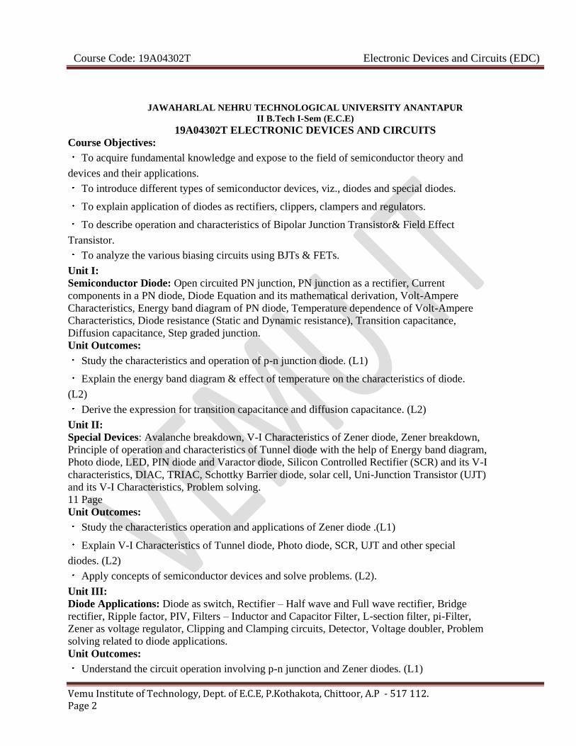
Let us consider the structure of Si. A Si atomic no. is 14 and it has 4 valance electrons. These 4
electrons are shared by four neighboring atoms in the crystal structure by means of covalent bond. Fig.
1.2a shows the crystal structure of Si at absolute zero temperature (0K). Hence a pure SC acts has poor
conductivity (due to lack of free electrons) at low or absolute zero temperature.
Covalent bond
Valence electron
Fig. 1.2a crystal structure of Si at 0K
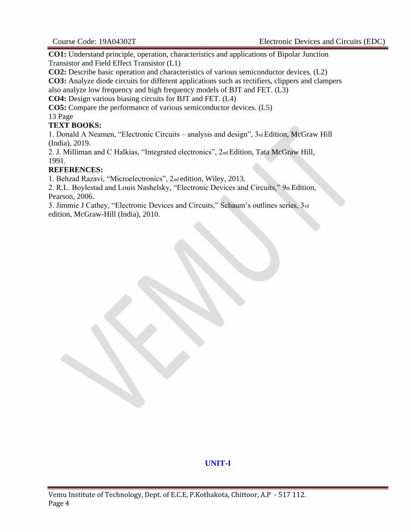
At room temperature some of the covalent bonds break up to thermal energy as shown in fig
1.2b. The valance electrons that jump into conduction band are called as free electrons that are available
for conduction.
Free electron
Valance electron
hole
Fig. 1.2b crystal structure of Si at room temperature0K

Course Code: 19A04302T Electronic Devices and Circuits (EDC)
Vemu Institute of Technology, Dept. of E.C.E, P.Kothakota, Chittoor, A.P - 517 112. Page 8
The absence of electrons in covalent bond is represented by a small circle usually referred to as
hole which is of positive charge. Even a hole serves as carrier of electricity in a manner similar to that of
free electron.
The mechanism by which a hole contributes to conductivity is explained as follows:
When a bond is in complete so that a hole exists, it is relatively easy for a valance electron in the
neighboring atom to leave its covalent bond to fill this hole. An electron moving from a bond to fill a
hole moves in a direction opposite to that of the electron. This hole, in its new position may now be
filled by an electron from another covalent bond and the hole will correspondingly move one more step
in the direction opposite to the motion of electron. Here we have a mechanism for conduction of
electricity which does not involve free electrons. This phenomenon is illustrated in fig1.3
Electron movement
Hole movement
Fig. 1.3a
Fig. 1.3b Fig. .3c

Course Code: 19A04302T Electronic Devices and Circuits (EDC)
Vemu Institute of Technology, Dept. of E.C.E, P.Kothakota, Chittoor, A.P - 517 112. Page 9
Fig 1.3a show that there is a hole at ion 6.Imagine that an electron from ion 5 moves into the
hole at ion 6 so that the configuration of 1.3b results. If we compare both fig1.3a &fig 1.3b, it appears as
if the hole has moved towards the left from ion6 to ion 5. Further if we compare fig 1.3b and fig 1.3c,
the hole moves from ion5 to ion 4. This discussion indicates the motion of hole is in a direction opposite
to that of motion of electron. Hence we consider holes as physical entities whose movement constitutes
flow of current.
In a pure semiconductor, the number of holes is equal to the number of free electrons.
1.0.2 EXTRINSIC SEMICONDUCTOR
Intrinsic semiconductor has very limited applications as they conduct very small amounts of
current at room temperature. The current conduction capability of intrinsic semiconductor can be
increased significantly by adding a small amounts impurity to the intrinsic semiconductor. By adding
impurities it becomes impure or extrinsic semiconductor. This process of adding impurities is called as
doping. The amount of impurity added is 1 part in 106 atoms.
N type semiconductor: If the added impurity is a pentavalent atom then the resultant semiconductor is
called N-type semiconductor. Examples of pentavalent impurities are Phosphorus, Arsenic, Bismuth,
Antimony etc.
A pentavalent impurity has five valance electrons. Fig 1.4a shows the crystal structure of N-type
semiconductor material where four out of five valance electrons of the impurity atom(antimony) forms
covalent bond with the four intrinsic semiconductor atoms. The fifth electron is loosely bound to the
impurity atom. This loosely bound electron can be easily
Fifth valance electron of SB
CB
Ec
Ed
Donor energy level
Ev
VB
Fig. 1.4a crystal structure of N type
SC
Fig. 1.4bEnergy band diagram of N
type

Course Code: 19A04302T Electronic Devices and Circuits
(EDC)
Vemu Institute of Technology, Dept. of E.C.E, P.Kothakota, Chittoor, A.P - 517 112. Page 10
Excited from the valance band to the conduction band by the application of electric field or increasing
the thermal energy. The energy required to detach the fifth electron form the impurity atom is very
small of the order of 0.01ev for Ge and 0.05 eV for Si.
The effect of doping creates a discrete energy level called donor energy level in the forbidden
band gap with energy level Ed slightly less than the conduction band (fig 1.4b). The difference
between the energy levels of the conducting band and the donor energy level is the energy required to
free the fifth valance electron (0.01 eV for Ge and 0.05 eV for Si). At room temperature almost all the
fifth electrons from the donor impurity atom are raised to conduction band and hence the number of
electrons in the conduction band increases significantly. Thus every antimony atom contributes to one
conduction electron without creating a hole.
In the N-type sc the no. of electrons increases and the no. of holes decreases compared to those
available in an intrinsic sc. The reason for decrease in the no. of holes is that the larger no. of electrons
present increases the recombination of electrons with holes. Thus current in N type sc is dominated by
electrons which are referred to as majority carriers. Holes are the minority carriers in N type sc
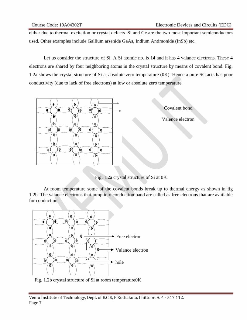
P type semiconductor: If the added impurity is a trivalent atom then the resultant semiconductor is
called P-type semiconductor. Examples of trivalent impurities are Boron, Gallium , indium etc.
Fig. 1.5a crystal structure of P type sc
The crystal structure of p type sc is shown in the fig1.5a. The three valance electrons of the
impurity (boon) forms three covalent bonds with the neighboring atoms and a vacancy exists in the
fourth bond giving rise to the holes. The hole is ready to accept an electron from the neighboring
Course Code: 19A04302T Electronic Devices and Circuits
(EDC)
Vemu Institute of Technology, Dept. of E.C.E, P.Kothakota, Chittoor, A.P - 517 112. Page 11
atoms. Each trivalent atom contributes to one hole generation and thus introduces a large no. of holes
in the valance band. At the same time the no. electrons are decreased compared to those available in
intrinsic sc because of increased recombination due to creation of additional holes.
Thus in P type sc , holes are majority carriers and electrons are minority carriers. Since each
trivalent impurity atoms are capable accepting an electron, these are called as acceptor atoms. The
following fig 1.5b shows the pictorial representation of P type sc
hole (majority carrier)
Electron (minority carrier)
Acceptor atoms
Fig. 1.5b crystal structure of P type sc
• The conductivity of N type sc is greater than that of P type sc as the mobility of electron is greater than that of hole.
• For the same level of doping in N type sc and P type sc, the conductivity of an Ntype sc is around twice that of a P type sc
1.0.3 CONDUCTIVITY OF SEMICONDUCTOR
In a pure sc, the no. of holes is equal to the no. of electrons. Thermal agitation continue to
produce new electron- hole pairs and the electron hole pairs disappear because of recombination. with
each electron hole pair created , two charge carrying particles are formed . One is negative which is a
free electron with mobility µn . The other is a positive i.e., hole with mobility µp . The electrons and
hole move in opppsitte direction in a an electric field E, but since they are of opposite sign, the current
due to each is in the same direction. Hence the total current density J within the intrinsic sc is given by
J = Jn + Jp =q n µn E + q p µp E
= (n µn + p
p)qE Where n=no. of electrons / unit volume i.e., concentration of free electrons

Course Code: 19A04302T Electronic Devices and Circuits
(EDC)
Vemu Institute of Technology, Dept. of E.C.E, P.Kothakota, Chittoor, A.P - 517 112. Page 12
P= no. of holes / unit volume i.e., concentration of holes
E=applied electric field strength, V/m
q= charge of electron or hole I n Coulombs Conductivity in extrinsic sc (N Type and P Type):
The conductivity of intrinsic sc is given by ςi= ni ( µn + µp) q = (n µn + p µp)q For N type , n>>p Therefore = q n µn
For P type ,p>>n Therefore = q p µp
1.0.4 CHARGE DENSITIES IN P TYPE AND N TYPE SEMICONDUCTOR: Mass Action Law:
Under thermal equilibrium for any semiconductor, the product of the no. of holes and the
concentration of electrons is constant and is independent of amount of donor and acceptor impurity
doping.
n.p= ni2
where n= eleetron concentration
p = hole concentration
ni2= intrinsic concentration
Hence in N type sc , as the no. of electrons increase the no. of holes decreases. Similarly in P type as
the no. of holes increases the no. of electrons decreases. Thus the product is constant and is equal to ni2
in case of intrinsic as well as extrinsic sc.
The law of mass action has given the relationship between free electrons concentration and
hole concentration. These concentrations are further related by the law of electrical neutrality as
explained below.
1.1 QUANTITATIVE THEORY OF PN JUNCTION DIODE
1.1.1 PN JUNCTION WITH NO APPLIED VOLTAGE OR OPEN CIRCUIT CONDITION:
In a piece of sc, if one half is doped by p type impurity and the other half is doped by n type
impurity, a PN junction is formed. The plane dividing the two halves or zones is called PN junction.
As shown in the fig the n type material has high concentration of free electrons, while p type material
has high concentration of holes. Therefore at the junction there is a tendency of free electrons to

Course Code: 19A04302T Electronic Devices and Circuits
(EDC)
Vemu Institute of Technology, Dept. of E.C.E, P.Kothakota, Chittoor, A.P - 517 112. Page 13
diffuse over to the P side and the holes to the N side. This process is called diffusion. As the free
electrons move across the junction from N type to P type, the donor atoms become positively charged.
Hence a positive charge is built on the N-side of the junction. The free electrons that cross the junction
uncover the negative acceptor ions by filing the holes. Therefore a negative charge is developed on the
p –side of the junction..This net negative charge on the p side prevents further diffusion of electrons
into the p side. Similarly the net positive charge on the N side repels the hole crossing from p side to N
side. Thus a barrier sis set up near the junction which prevents the further movement of charge carriers
i.e. electrons and holes. As a consequence of induced electric field across the depletion layer, an
electrostatic potential difference is established between P and N regions, which are called the potential
barrier, junction barrier, diffusion potential or contact potential, Vo. The magnitude of the contact
potential Vo varies with doping levels and temperature. Vo is 0.3V for Ge and 0.72 V for Si.
Fig 1.6: Symbol of PN Junction Diode
The electrostatic field across the junction caused by the positively charged N-Type region
tends to drive the holes away from the junction and negatively charged p type regions tend to drive the
electrons away from the junction. The majority holes diffusing out of the P region leave behind
negatively charged acceptor atoms bound to the lattice, thus exposing a negatives pace charge in a
previously neutral region. Similarly electrons diffusing from the N region expose positively ionized
donor atoms and a double space charge builds up at the junction as shown in the fig. 1.7a
It is noticed that the space charge layers are of opposite sign to the majority carriers diffusing
into them, which tends to reduce the diffusion rate. Thus the double space of the layer causes an
electric field to be set up across the junction directed from N to P regions, which is in such a direction
to inhibit the diffusion of majority electrons and holes as illustrated in fig 1.7b. The shape of the
charge density, ρ, depends upon how diode id doped. Thus the junction region is depleted of mobile

Course Code: 19A04302T Electronic Devices and Circuits
(EDC)
Vemu Institute of Technology, Dept. of E.C.E, P.Kothakota, Chittoor, A.P - 517 112. Page 14
charge carriers. Hence it is called depletion layer, space region, and transition region. The depletion
region is of the order of 0.5µm thick. There are no mobile carriers in this narrow depletion region.
Hence no current flows across the junction and the system is in equilibrium. To the left of this
depletion layer, the carrier concentration is p= NA and to its right it is n= ND.
Fig 1.7b
1.1.2 FORWARD BIASED JUNCTION DIODE
When a diode is connected in a Forward Bias condition, a negative voltage is applied to the
N-type material and a positive voltage is applied to the P-type material. If this external voltage
becomes greater than the value of the potential barrier, approx. 0.7 volts for silicon and 0.3 volts for
germanium, the potential barriers opposition will be overcome and current will start to flow. This is
because the negative voltage pushes or repels electrons towards the junction giving them the energy to
cross over and combine with the holes being pushed in the opposite direction towards the junction by
the positive voltage. This results in a characteristics curve of zero current flowing up to this voltage
point, called the "knee" on the static curves and then a high current flow through the diode with little

Course Code: 19A04302T Electronic Devices and Circuits
(EDC)
Vemu Institute of Technology, Dept. of E.C.E, P.Kothakota, Chittoor, A.P - 517 112. Page 15
increase in the external voltage as shown below.
Forward Characteristics Curve for a Junction Diode
Fig 1.8a: Diode Forward Characteristics
The application of a forward biasing voltage on the junction diode results in the depletion layer
becoming very thin and narrow which represents a low impedance path through the junction thereby
allowing high currents to flow. The point at which this sudden increase in current takes place is
represented on the static I-V characteristics curve above as the "knee" point.
Forward Biased Junction Diode showing a Reduction in the Depletion Layer

Course Code: 19A04302T Electronic Devices and Circuits
(EDC)
Vemu Institute of Technology, Dept. of E.C.E, P.Kothakota, Chittoor, A.P - 517 112. Page 16
Fig 1.8b: Diode Forward Bias

Course Code: 19A04302T Electronic Devices and Circuits
(EDC)
Vemu Institute of Technology, Dept. of E.C.E, P.Kothakota, Chittoor, A.P - 517 112. Page 17
This condition represents the low resistance path through the PN junction allowing very large currents
to flow through the diode with only a small increase in bias voltage. The actual potential difference
across the junction or diode is kept constant by the action of the depletion layer at approximately 0.3v
for germanium and approximately 0.7v for silicon junction diodes. Since the diode can conduct
"infinite" current above this knee point as it effectively becomes a short circuit, therefore resistors are
used in series with the diode to limit its current flow. Exceeding its maximum forward current
specification causes the device to dissipate more power in the form of heat than it was designed for
resulting in a very quick failure of the device.
1.1.2 PN JUNCTION UNDER REVERSE BIAS CONDITION:
Reverse Biased Junction Diode:
When a diode is connected in a Reverse Bias condition, a positive voltage is applied to the N-
type material and a negative voltage is applied to the P-type material. The positive voltage applied to
the N-type material attracts electrons towards the positive electrode and away from the junction, while
the holes in the P-type end are also attracted away from the junction towards the negative electrode.
The net result is that the depletion layer grows wider due to a lack of electrons and holes and presents
a high impedance path, almost an insulator. The result is that a high potential barrier is created thus
preventing current from flowing through the semiconductor material.
Reverse Biased Junction Diode showing an Increase in the Depletion
Fig 1.9a: Diode Reverse Bias

Course Code: 19A04302T Electronic Devices and Circuits
(EDC)
Vemu Institute of Technology, Dept. of E.C.E, P.Kothakota, Chittoor, A.P - 517 112. Page 18
This condition represents a high resistance value to the PN junction and practically zero current
flows through the junction diode with an increase in bias voltage. However, a very small leakage
current does flow through the junction which can be measured in microamperes, (μA). One final point,
if the reverse bias voltage Vr applied to the diode is increased to a sufficiently high enough value, it will
cause the PN junction to overheat and fail due to the avalanche effect around the junction. This may
cause the diode to become shorted and will result in the flow of maximum circuit current and this
shown as a step downward slope in the reverse static characteristics curve below.
Reverse Characteristics Curve for a Junction Diode
Fig 1.9b: Diode Reverse Characteristics
Sometimes this avalanche effect has practical applications in voltage stabilizing circuits where a series
limiting resistor is used with the diode to limit this reverse breakdown current to a preset maximum
value thereby producing a fixed voltage output across the diode. These types of diodes are commonly
known as Zener Diodes

Course Code: 19A04302T Electronic Devices and Circuits
(EDC)
Vemu Institute of Technology, Dept. of E.C.E, P.Kothakota, Chittoor, A.P - 517 112. Page 19
1.2 VI CHARACTERISTICS AND THEIR TEMPERATURE DEPENDENCE
Diode terminal characteristics equation for diode junction current:
=
−1TV
V
OD eII
Where VT = KT/q;
VD_ diode terminal voltage, Volts
Io _ temperature-dependent saturation current, µA
T _ absolute temperature of p-n junction, K
K _ Boltzmann’s constant 1.38x 10 -
23J/K) q _ electron charge 1.6x10⁻¹⁹ C
= empirical constant, 1 for Ge and 2 for Si
Fig 1.10: Diode Characteristics
Temperature Effects on Diode
Temperature can have a marked effect on the characteristics of a silicon semiconductor diode
as shown in Fig. 11 It has been found experimentally that the reverse saturation current Io will just
about double in magnitude for every 10°C increase in temperature.

Course Code: 19A04302T Electronic Devices and Circuits (EDC)
Vemu Institute of Technology, Dept. of E.C.E, P.Kothakota, Chittoor, A.P - 517 112. Page 20
Fig 1.11 Variation in Diode Characteristics with temperature change
It is not uncommon for a germanium diode with an Io in the order of 1 or 2 A at 25°C to have a
leakage current of 100 A - 0.1 mA at a temperature of 100°C. Typical values of Io for silicon are much
lower than that of germanium for similar power and current levels. The result is that even at high
temperatures the levels of Io for silicon diodes do not reach the same high levels obtained. For
germanium—a very important reason that silicon devices enjoy a significantly higher level of
development and utilization in design. Fundamentally, the open-circuit equivalent in the reverse bias
region is better realized at any temperature with silicon than with germanium. The increasing levels of Io
with temperature account for the lower levels of threshold voltage, as shown in Fig. 1.11. Simply
increase the level of Io in and not rise in diode current. Of course, the level of TK also will be increase,
but the increasing level of Io will overpower the smaller percent change in TK. As the temperature
increases the forward characteristics are actually becoming more “ideal,”
1.3 IDEAL VERSUS PRACTICAL RESISTANCE LEVELS
DC or Static Resistance
The application of a dc voltage to a circuit containing a semiconductor diode will result in an
operating point on the characteristic curve that will not change with time. The resistance of the diode
at the operating point can be found simply by finding the corresponding levels of VD and ID as shown
in Fig. 1.12 and applying the following Equation:
The dc resistance levels at the knee and below will be greater than the resistance levels obtained for

Course Code: 19A04302T Electronic Devices and Circuits (EDC)
Vemu Institute of Technology, Dept. of E.C.E, P.Kothakota, Chittoor, A.P - 517 112. Page 21
the vertical rise section of the characteristics. The resistance levels in the reverse-bias region will
naturally be quite high. Since ohmmeters typically employ a relatively constant-current source, the
resistance determined will be at a preset current level (typically, a few mill amperes).
Fig 1.12 Determining the dc resistance of a diode at a particular operating point.
AC or Dynamic Resistance
It is obvious from Eq. 1.3 that the dc resistance of a diode is independent of the shape of the
characteristic in the region surrounding the point of interest. If a sinusoidal rather than dc input is
applied, the situation will change completely. The varying input will move the instantaneous operating
point up and down a region of the characteristics and thus defines a specific change in current and
voltage as shown in Fig. 1.13. With no applied varying signal, the point of operation would be the Q-
point appearing on Fig. 1.13 determined by the applied dc levels. The designation Q-point is derived
from the word quiescent, which means “still or unvarying.” A straight-line drawn tangent to the curve
through the Q-point as shown in Fig. 1.13 will define a particular change in voltage and current that can
be used to determine the ac or dynamic resistance for this region of the diode characteristics. In equation
form,
Where Signifies a finite change in the quantity
Fig 1.13: Determining the ac resistance of a diode at a particular operating point.
1.4 DIODE EQUIVALENT CIRCUITS

Course Code: 19A04302T Electronic Devices and Circuits (EDC)
Vemu Institute of Technology, Dept. of E.C.E, P.Kothakota, Chittoor, A.P - 517 112. Page 22
An equivalent circuit is a combination of elements properly chosen to best represent the actual
terminal characteristics of a device, system, or such in a particular operating region. In other words,
once the equivalent circuit is defined, the device symbol can be removed from a schematic and the
equivalent circuit inserted in its place without severely affecting the actual behavior of the system. The
result is often a network that can be solved using traditional circuit analysis techniques.
Piecewise-Linear Equivalent Circuit
One technique for obtaining an equivalent circuit for a diode is to approximate the characteristics
of the device by straight-line segments, as shown in Fig. 1.31. The resulting equivalent circuit is
naturally called the piecewise-linear equivalent circuit. It should be obvious from Fig. 1.31 that the
straight-line segments do not result in an exact duplication of the actual characteristics, especially in the
knee region. However, the resulting segments are sufficiently close to the actual curve to establish an
equivalent circuit that will provide an excellent first approximation to the actual behavior of the device.
The ideal diode is included to establish that there is only one direction of conduction through the device,
and a reverse-bias condition will result in the open- circuit state for the device. Since a silicon
semiconductor, diode does not reach the conduction state until VD reaches 0.7 V with a forward bias (as
shown in Fig. 1.14a), a battery VT opposing the conduction direction must appear in the equivalent
circuit as shown in Fig. 1.14b. The battery simply specifies that the voltage across the device must be
greater than the threshold battery voltage before conduction through the device in the direction dictated
by the ideal diode can be established. When conduction is established, the resistance of the diode will be
the specified value of rav.
Fig: 1.14aDiode piecewise-linear model characteristics

Course Code: 19A04302T Electronic Devices and Circuits (EDC)
Vemu Institute of Technology, Dept. of E.C.E, P.Kothakota, Chittoor, A.P - 517 112. Page 23
Fig: 1.14b Diode piecewise-linear model equivalent circuit The approximate level of rav can usually be determined from a specified operating point on the
specification sheet. For instance, for a silicon semiconductor diode, if IF _ 10 mA (a forward conduction
current for the diode) at VD _ 0.8 V, we know for silicon that a shift of 0.7 V is required before the
characteristics rise.
Fig 1.15 Ideal Diode and its characteristics
Fig 1.16: Diode equivalent circuits (models)

Course Code: 19A04302T Electronic Devices and Circuits (EDC)
Vemu Institute of Technology, Dept. of E.C.E, P.Kothakota, Chittoor, A.P - 517 112. Page 24
1.5 TRANSITION AND DIFFUSION CAPACITANCE
Electronic devices are inherently sensitive to very high frequencies. Most shunt capacitive
effects that can be ignored at lower frequencies because the reactance XC=1/2πfC is very large (open-
circuit equivalent). This, however, cannot be ignored at very high frequencies. XC will become
sufficiently small due to the high value of f to introduce a low-reactance “shorting” path. In the p-n
semiconductor diode, there are two capacitive effects to be considered. In the reverse-bias region we
have the transition- or depletion region capacitance (CT), while in the forward-bias region we have the
diffusion (CD) or storage capacitance. Recall that the basic equation for the capacitance of a parallel-
plate capacitor is defined by C=€A/d, where € is the permittivity of the dielectric (insulator) between the
plates of area A separated by a distance d. In the reverse-, bias region there is a depletion region (free of
carriers) that behaves essentially like an insulator between the layers of opposite charge. Since the
depletion width (d) will increase with increased reverse-bias potential, the resulting transition
capacitance will decrease. The fact that the capacitance is dependent on the applied reverse-bias
potential has application in a number of electronic systems. Although the effect described above will
also be present in the forward-bias region, it is over shadowed by a capacitance effect directly dependent
on the rate at which charge is injected into the regions just outside the depletion region. The capacitive
effects described above are represented by a capacitor in parallel with the ideal diode, as shown in Fig.
1.38. For low- or mid-frequency applications (except in the power area), however, the capacitor is
normally not included in the diode symbol.
Fig 1.17: Including the effect of the transition or diffusion capacitance on the semiconductor diode
Diode capacitances: The diode exhibits two types of capacitances transition capacitance and diffusion
capacitance.
• Transition capacitance: The capacitance which appears between positive ion layer in n-region and negative ion layer in p-region.
• Diffusion capacitance: This capacitance originates due to diffusion of charge carriers in the opposite regions.
The transition capacitance is very small as compared to the diffusion capacitance. In reverse bias transition, the capacitance is the dominant and is given by:

Course Code: 19A04302T Electronic Devices and Circuits (EDC)
Vemu Institute of Technology, Dept. of E.C.E, P.Kothakota, Chittoor, A.P - 517 112. Page 25
where CT - transition capacitance
A - diode cross sectional area
W - depletion region width In forward bias, the diffusion capacitance is the dominant and is given by: where CD - diffusion capacitance
dQ - change in charge stored in depletion region
V - change in applied voltage
- time interval for change in voltage
g - diode conductance
r - diode resistance The diffusion capacitance at low frequencies is given by the formula:
The diffusion capacitance at high frequencies is inversely proportional to the frequency and is given by
the formula:
Note: The variation of diffusion capacitance with applied voltage is used in the design of varactor.
1.6 BREAK DOWN MECHANISMS
When an ordinary P-N junction diode is reverse biased, normally only very small reverse
saturation current flows. This current is due to movement of minority carriers. It is almost independent
of the voltage applied. However, if the reverse bias is increased, a point is reached when the junction
breaks down and the reverse current increases abruptly. This current could be large enough to destroy
the junction. If the reverse current is limited by means of a suitable series resistor, the power dissipation
at the junction will not be excessive, and the device may be operated continuously in its breakdown
region to its normal (reverse saturation) level. It is found that for a suitably designed diode, the

Course Code: 19A04302T Electronic Devices and Circuits (EDC)
Vemu Institute of Technology, Dept. of E.C.E, P.Kothakota, Chittoor, A.P - 517 112. Page 26
breakdown voltage is very stable over a wide range of reverse currents. This quality gives the
breakdown diode many useful applications as a voltage reference source.
The critical value of the voltage, at which the breakdown of a P-N junction diode occurs, is called the
breakdown voltage. The breakdown voltage depends on the width of the depletion region, which, in
turn, depends on the doping level. The junction offers almost zero resistance at the breakdown point.
There are two mechanisms by which breakdown can occur at a reverse biased P-N junction:
1. avalanche breakdown and
2. Zener breakdown.
Avalanche breakdown
The minority carriers, under reverse biased conditions, flowing through the junction acquire a
kinetic energy which increases with the increase in reverse voltage. At a sufficiently high reverse
voltage (say 5 V or more), the kinetic energy of minority carriers becomes so large that they knock out
electrons from the covalent bonds of the semiconductor material. As a result of collision, the liberated
electrons in turn liberate more electrons and the current becomes very large leading to the breakdown of
the crystal structure itself. This phenomenon is called the avalanche breakdown. The breakdown region
is the knee of the characteristic curve. Now the current is not controlled by the junction voltage but
rather by the external circuit.
Zener breakdown
Fig 1.18: Diode characteristics with breakdown
Under a very high reverse voltage, the depletion region expands and the potential barrier
increases leading to a very high electric field across the junction. The electric field will break some of
the covalent bonds of the semiconductor atoms leading to a large number of free minority carriers,

Course Code: 19A04302T Electronic Devices and Circuits (EDC)
Vemu Institute of Technology, Dept. of E.C.E, P.Kothakota, Chittoor, A.P - 517 112. Page 27
which suddenly increase the reverse current.
This is called the Zener effect. The breakdown occurs at a particular and constant value of
reverse voltage called the breakdown voltage, it is found that Zener breakdown occurs at electric field
intensity of about 3 x 10⁷ V/m.
Either of the two (Zener breakdown or avalanche breakdown) may occur independently, or both
of these may occur simultaneously. Diode junctions that breakdown below 5 V are caused by Zener
effect. Junctions that experience breakdown above 5 V are caused by avalanche effect. Junctions that
breakdown around 5 V are usually caused by combination of two effects. The Zener breakdown occurs
in heavily doped junctions (P-type semiconductor moderately doped and N-type heavily doped), which
produce narrow depletion layers. The avalanche breakdown occurs in lightly doped junctions, which
produce wide depletion layers. With the increase in junction temperature Zener breakdown voltage is
reduced while the avalanche breakdown voltage increases. The Zener diodes have a negative
temperature coefficient while avalanche diodes have a positive temperature coefficient. Diodes that have
breakdown voltages around 5 V have zero temperature coefficient. The breakdown phenomenon is
reversible and harmless so long as the safe operating temperature is maintained.
1.7 ZENER DIODES
The Zener diode is like a general-purpose signal diode consisting of a silicon PN junction.
When biased in the forward direction it behaves just like a normal signal diode passing the rated current,
but as soon as a reverse voltage applied across the zener diode exceeds the rated voltage of the device,
the diodes breakdown voltage VB is reached at which point a process called Avalanche Breakdown
occurs in the semiconductor depletion layer and a current starts to flow through the diode to limit this
increase in voltage.
The current now flowing through the zener diode increases dramatically to the maximum circuit
value (which is usually limited by a series resistor) and once achieved this reverse saturation current
remains fairly constant over a wide range of applied voltages. This breakdown voltage point, VB is
called the "zener voltage" for zener diodes and can range from less than one volt to hundreds of volts.
The point at which the zener voltage triggers the current to flow through the diode can be very
accurately controlled (to less than 1% tolerance) in the doping stage of the diodes semiconductor
construction giving the diode a specific zener breakdown voltage, (Vz) for example, 4.3V or 7.5V. This
zener breakdown voltage on the I-V curve is almost a vertical straight line.

Course Code: 19A04302T Electronic Devices and Circuits (EDC)
Vemu Institute of Technology, Dept. of E.C.E, P.Kothakota, Chittoor, A.P - 517 112. Page 28
Zener Diode I-V Characteristics
Fig 1.19 : Zener diode characteristics
The Zener Diode is used in its "reverse bias" or reverse breakdown mode, i.e. the diodes anode
connects to the negative supply. From the I-V characteristics curve above, we can see that the zener
diode has a region in its reverse bias characteristics of almost a constant negative voltage regardless of
the value of the current flowing through the diode and remains nearly constant even with large changes
in current as long as the zener diodes current remains between the breakdown current IZ(min) and the
maximum current rating IZ(max).
This ability to control itself can be used to great effect to regulate or stabilize a voltage source
against supply or load variations. The fact that the voltage across the diode in the breakdown region is
almost constant turns out to be an important application of the zener diode as a voltage regulator. The
function of a regulator is to provide a constant output voltage to a load connected in parallel with it in
spite of the ripples in the supply voltage or the variation in the load current and the zener diode will
continue to regulate the voltage until the diodes current falls below the minimum IZ(min) value in the

Course Code: 19A04302T Electronic Devices and Circuits (EDC)
Vemu Institute of Technology, Dept. of E.C.E, P.Kothakota, Chittoor, A.P - 517 112. Page 29
reverse breakdown region.
SPECIAL PURPOSE ELECTRONIC DEVICES
1.8 PRINCIPLE OF OPERATION AND CHARACTERISTICS OF TUNNEL DIODE
A tunnel diode or Esaki diode is a type of semiconductor diode which is capable of very fast operation,
well into the microwave frequency region, by using quantum mechanical effects.
It was invented in August 1957 by Leo Esaki when he was with Tokyo Tsushin Kogyo, now known as
Sony. In 1973 he received the Nobel Prize in Physics, jointly with Brian Josephson, for discovering the
electron tunneling effect used in these diodes. Robert Noyce independently came up with the idea of a
tunnel diode while working for William Shockley, but was discouraged from pursuing it.
Fig 1.19: Tunnel diode schematic symbol
These diodes have a heavily doped p–n junction only some 10 nm (100 Å) wide. The heavy doping
results in a broken band gap, where conduction band electron states on the n-side are more or less
aligned with valence band hole states on the p-side. Tunnel diodes were manufactured by Sony for the
first time in 1957 followed by General Electric and other companies from about 1960, and are still made
in low volume today. Tunnel diodes are usually made from germanium, but can also be made in gallium
arsenide and silicon materials. They can be used as oscillators, amplifiers, frequency converters and
detectors.
Tunneling Phenomenon:
In a conventional semiconductor diode, conduction takes place while the p–n junction is forward
biased and blocks current flow when the junction is reverse biased. This occurs up to a point known as
the “reverse breakdown voltage” when conduction begins (often accompanied by destruction of the
device). In the tunnel diode, the dopant concentration in the p and n layers are increased to the point
where the reverse breakdown voltage becomes zero and the diode conducts in the reverse direction.
However, when forward-biased, an odd effect occurs called “quantum mechanical tunneling” which
gives rise to a region where an increase in forward voltage is accompanied by a decrease in forward
current.
Forward bias operation

Course Code: 19A04302T Electronic Devices and Circuits (EDC)
Vemu Institute of Technology, Dept. of E.C.E, P.Kothakota, Chittoor, A.P - 517 112. Page 30
Under normal forward bias operation, as voltage begins to increase, electrons at first tunnel through the
very narrow p–n junction barrier because filled electron states in the conduction band on the n-

Course Code: 19A04302T Electronic Devices and Circuits (EDC)
Vemu Institute of Technology, Dept. of E.C.E, P.Kothakota, Chittoor, A.P - 517 112. Page 31
side become aligned with empty valence band hole states on the p-side of the p-n junction. As voltage
increases further these states become more misaligned and the current drops – this is called negative
resistance because current decreases with increasing voltage. As voltage increases yet further, the diode
begins to operate as a normal diode, where electrons travel by conduction across the p–n junction, and
no longer by tunneling through the p–n junction barrier. Thus the most important operating region for a
tunnel diode is the negative resistance region.
Reverse bias operation
When used in the reverse direction they are called back diodes and can act as fast rectifiers with
zero offset voltage and extreme linearity for power signals (they have an accurate square law
characteristic in the reverse direction).
Under reverse bias filled states on the p-side become increasingly aligned with empty states on
the n-side and electrons now tunnel through the pn junction barrier in reverse direction – this is the
Zener effect that also occurs in zener diodes.
Technical comparisons
Fig 1.20a: current-voltage characteristic of tunnel diode
A rough approximation of the V-I curve for a tunnel diode, showing the negative differential
resistance region. The Japanese physicist Leo Esaki invented the tunnel diode in 1958.It consists of a p-n
junction with highly doped regions. Because of the thinness of the junction, the electrons can pass

Course Code: 19A04302T Electronic Devices and Circuits (EDC)
Vemu Institute of Technology, Dept. of E.C.E, P.Kothakota, Chittoor, A.P - 517 112. Page 32
through the potential barrier of the dam layer at a suitable polarization, reaching the energy states on the
other sides of the junction. The current-voltage characteristic of the diode is represented in Figure 1.20a.
In this sketch i p and Up are the peak, and iv and Uv are the valley values for the current and voltage
respectively. The form of this dependence can be qualitatively explained by considering the tunneling
processes that take place in a thin p-n junction.
Energy band structure of tunnel diode:
Fig 1.20b Energy band structure of tunnel diode For the degenerated semiconductors, the energy band diagram at thermal equilibrium is presented in Figure 1.20b. In Figure 1.20c the tunneling processes in different points of the current voltage characteristic for the tunnel diode are presented.

Course Code: 19A04302T Electronic Devices and Circuits (EDC)
Vemu Institute of Technology, Dept. of E.C.E, P.Kothakota, Chittoor, A.P - 517 112. Page 33
Advantages of tunnel diodes:
• Environmental immunity i.e. peak point is not a function of temperature.
• Low cost.
• Low noise.
• Low power consumption.
• High speed i.e. tunneling takes place very fast at the speed of light in the order of nanoseconds • Simplicity i.e. a tunnel diode can be used along with a d.c supply and a few passive elements to
obtain various application circuits.
Applications for tunnel diodes:
• local oscillators for UHF television tuners
• Trigger circuits in oscilloscopes
• High speed counter circuits and very fast-rise time pulse generator circuits
• The tunnel diode can also be used as low-noise microwave amplifier.
1.9 VARACTOR DIODE
Varactor diode is a special type of diode which uses transition capacitance property i.e voltage variable
capacitance .These are also called as varicap, VVC(voltage variable capacitance) or tuning diodes.
The varactor diode symbol is shown below with a diagram representation.
Fig 1.21a: symbol of varactor diode
When a reverse voltage is applied to a PN junction, the holes in the p-region are attracted to the anode
terminal and electrons in the n-region are attracted to the cathode terminal creating a region where there
is little current. This region , the depletion region, is essentially devoid of carriers and behaves as the
dielectric of a capacitor.
The depletion region increases as reverse voltage across it increases; and since capacitance
varies inversely as dielectric thickness, the junction capacitance will decrease as the voltage across the
PN junction increases. So by varying the reverse voltage across a PN junction the junction capacitance
can be varied .This is shown in the typical varactor voltage-capacitance curve below.

Course Code: 19A04302T Electronic Devices and Circuits (EDC)
Vemu Institute of Technology, Dept. of E.C.E, P.Kothakota, Chittoor, A.P - 517 112. Page 34
Fig 1.21b:voltage- capacitance curve
Notice the nonlinear increase in capacitance as the reverse voltage is decreased. This nonlinearity
allows the varactor to be used also as a harmonic generator.
Major varactor considerations are:
(a) Capacitance value
(b) Voltage
(c) Variation in capacitance with voltage.
(d) Maximum working voltage
(e) Leakage current
Applications:
• Tuned circuits. • FM modulators
• Automatic frequency control devices
• Adjustable bandpass filters
• Parametric amplifiers
• Television receivers.
1.10 PRINCIPLE OF OPERATION OF SCR
A silicon-controlled rectifier (or semiconductor-controlled rectifier) is a four-layer solid state
device that controls current. The name "silicon controlled rectifier" or SCR is General Electric's
trade name for a type of thyristor. The SCR was developed by a team of power engineers led by
Gordon Hall and commercialized by Frank W. "Bill" Gutzwiller in 1957.symbol of SCR is given
below:

Course Code: 19A04302T Electronic Devices and Circuits (EDC)
Vemu Institute of Technology, Dept. of E.C.E, P.Kothakota, Chittoor, A.P - 517 112. Page 35
Construction of SCR
An SCR consists of four layers of alternating P and N type semiconductor materials. Silicon is
used as the intrinsic semiconductor, to which the proper dopants are added. The junctions are either
diffused or alloyed. The planar construction is used for low power SCRs (and all the junctions are
diffused). The mesa type construction is used for high power SCRs. In this case, junction J2 is obtained
by the diffusion method and then the outer two layers are alloyed to it, since the PNPN pellet is required
to handle large currents. It is properly braced with tungsten or molybdenum plates to provide greater
mechanical strength. One of these plates is hard soldered to a copper stud, which is threaded for
attachment of heat sink. The doping of PNPN will depend on the application of SCR, since its
characteristics are similar to those of the thyratron. Today, the term thyristor applies to the larger family
of multilayer devices that exhibit bistable state-change behaviour, that is, switching either ON or OFF.
The operation of a SCR and other thyristors can be understood in terms of a pair of tightly
coupled bipolar junction transistors, arranged to cause the self-latching action.The following figures are
construction of SCR,its two transistor model and symbol respectively
Fig 1.23: Construction, Two transistor model of SCR and symbol of SCR
SCR Working Principle
Fig 1.24: Current flow and voltage bias in an SCR

Course Code: 19A04302T Electronic Devices and Circuits (EDC)
Vemu Institute of Technology, Dept. of E.C.E, P.Kothakota, Chittoor, A.P - 517 112. Page 36
The SCR is a four-layer, three-junction and a three-terminal device and is shown in fig.1.24. The
end P-region is the anode, the end N-region is the cathode and the inner P-region is the gate. The anode
to cathode is connected in series with the load circuit. Essentially the device is a switch. Ideally it
remains off (voltage blocking state), or appears to have an infinite impedance until both the anode and
gate terminals have suitable positive voltages with respect to the cathode terminal. The thyristor then
switches on and current flows and continues to conduct without further gate signals. Ideally the thyristor
has zero impedance in conduction state. For switching off or reverting to the blocking state, there must
be no gate signal and the anode current must be reduced to zero. Current can flow only in one direction.
In absence of external bias voltages, the majority carrier in each layer diffuses until there is a
built-in voltage that retards further diffusion. Some majority carriers have enough energy to cross the
barrier caused by the retarding electric field at each junction. These carriers then become minority
carriers and can recombine with majority carriers. Minority carriers in each layer can be accelerated
across each junction by the fixed field, but because of absence of external circuit in this case the sum of
majority and minority carrier currents must be zero.
A voltage bias, as shown in figure, and an external circuit to carry current allow internal currents which
include the following terms:
The current Ix is due to
• Majority carriers (holes) crossing junction J1
• Minority carriers crossing junction J1
• Holes injected at junction J2 diffusing through the N-region and crossing junction J1 and
• Minority carriers from junction J2 diffusing through the N-region and crossing junction J1.
As already mentioned, the SCR is a four-layer device with three terminals, namely, the anode, the
cathode and the gate. When the anode is made positive with respect to the cathode, junctions J1 and J3
are forward biased and junction J2 is reverse-biased and only the leakage current will flow through the
device. The SCR is then said to be in the forward blocking state or in the forward mode or off state. But
when the cathode is made positive with respect to the anode, junctions J1 and J3 are reverse-biased, a
small reverse leakage current will flow through the SCR and the SGR is said to be in the reverse
blocking state or in reverse mode.
Course Code: 19A04302T Electronic Devices and Circuits (EDC)
Vemu Institute of Technology, Dept. of E.C.E, P.Kothakota, Chittoor, A.P - 517 112. Page 37
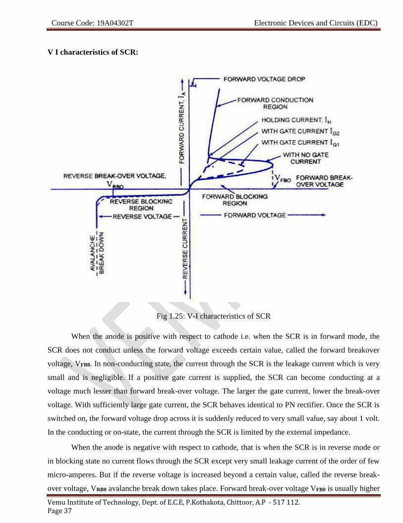
V I characteristics of SCR:
Fig 1.25: V-I characteristics of SCR
When the anode is positive with respect to cathode i.e. when the SCR is in forward mode, the
SCR does not conduct unless the forward voltage exceeds certain value, called the forward breakover
voltage, VFB0. In non-conducting state, the current through the SCR is the leakage current which is very
small and is negligible. If a positive gate current is supplied, the SCR can become conducting at a
voltage much lesser than forward break-over voltage. The larger the gate current, lower the break-over
voltage. With sufficiently large gate current, the SCR behaves identical to PN rectifier. Once the SCR is
switched on, the forward voltage drop across it is suddenly reduced to very small value, say about 1 volt.
In the conducting or on-state, the current through the SCR is limited by the external impedance.
When the anode is negative with respect to cathode, that is when the SCR is in reverse mode or
in blocking state no current flows through the SCR except very small leakage current of the order of few
micro-amperes. But if the reverse voltage is increased beyond a certain value, called the reverse break-
over voltage, VRB0 avalanche break down takes place. Forward break-over voltage VFB0 is usually higher

Course Code: 19A04302T Electronic Devices and Circuits (EDC)
Vemu Institute of Technology, Dept. of E.C.E, P.Kothakota, Chittoor, A.P - 517 112. Page 38
than reverse break over voltage, VRBO.
From the foregoing discussion, it can be seen that the SCR has two stable and reversible
operating states. The change over from off-state to on-state, called turn-on, can be achieved by
increasing the forward voltage beyond VFB0. A more convenient and useful method of turn-on the device
employs the gate drive. If the forward voltage is less than the forward break-over voltage, VFB0, it can be
turned-on by applying a positive voltage between the gate and the cathode. This method is called the
gate control. Another very important feature of the gate is that once the SCR is triggered to on-state the
gate loses its control.
The switching action of gate takes place only when
(i) SCR is forward biased i.e. anode is positive with respect to cathode, and
(ii) Suitable positive voltage is applied between the gate and the cathode.
Once the SCR has been switched on, it has no control on the amount of current flowing through it. The
current through the SCR is entirely controlled by the external impedance connected in the circuit and the
applied voltage. There is, however, a very small, about 1 V, potential drop across the SCR. The forward
current through the SCR can be reduced by reducing the applied voltage or by increasing the circuit
impedance. There is, however, a minimum forward current that must be maintained to keep the SCR in
conducting state. This is called the holding current rating of SCR. If the current through the SCR is
reduced below the level of holding current, the device returns to off-state or blocking state.
The SCR can be switched off by reducing the forward current below the level of holding current
which may be done either by reducing the applied voltage or by increasing the circuit impedance.
Alternatively the SCR can be switched off by applying negative voltage to the anode (reverse
mode), the SCR naturally will be switched off.
Here one point is worth mentioning, the SCR takes certain time to switch off. The time, called
the turn-off time, must be allowed before forward voltage may be applied again otherwise the device
will switch-on with forward voltage without any gate pulse. The turn-off time is about 15 micro-
seconds, which is immaterial when dealing with power frequency, but this becomes important in the
inverter circuits, which are to operate at high frequency.
Merits of SCR

Course Code: 19A04302T Electronic Devices and Circuits (EDC)
Vemu Institute of Technology, Dept. of E.C.E, P.Kothakota, Chittoor, A.P - 517 112. Page 39
1. Very small amount of gate drive is required.
2. SCRs with high voltage and current ratings are available.
3. On state losses of SCR are less.
Demerits of SCR
1. Gate has no control, once SCR is turned on.
2. External circuits are required for turning it off.
3. Operating frequencies are low.
4. Additional protection circuits are required.
Application of SCRs
SCRs are mainly used in devices where the control of high power, possibly coupled with high
voltage, is demanded. Their operation makes them suitable for use in medium to high-voltage AC power
control applications, such as lamp dimming, regulators and motor control.
SCRs and similar devices are used for rectification of high power AC in high-voltage direct
current power transmission
1.11 PHOTO DIODE
The photo diode is a semiconductor p-n junction device whose region of operation is limited to the
reverse biased region. The figure below shows the symbol of photodiode
Fig 1.26: Symbol of photodiode.
Principle of operation:
A photodiode is a type of photo detector capable of converting light into either current or
voltage, depending upon the mode of operation. The common, traditional solar cell used to generate
electric solar power is a large area photodiode. A photodiode is designed to operate in reverse bias. The
deletion region width is large. Under normal conditions it carries small reverse current due to minority
charge carriers. When light is incident through glass window on the p-n junction, photons in the light
bombard the p-n junction and some energy s imparted to the valence electrons. So valence electrons

Course Code: 19A04302T Electronic Devices and Circuits (EDC)
Vemu Institute of Technology, Dept. of E.C.E, P.Kothakota, Chittoor, A.P - 517 112. Page 40
break covalent bonds and become free electrons. Thus more electron-hole pairs are generated. Thus
total number of minority charge carriers increases and hence reverse current increases. This is the basic
principle of operation of photo diode.
Fig 1.27: Basic Biasing Arrangement and construction of photodiode and symbols
Characteristics of photodiode:
When the P-N junction is reverse-biased, a reverse saturation current flows due to thermally
generated holes and electrons being swept across the junction as the minority carriers. With the increase
in temperature of the junction more and more hole-electron pairs are created and so the reverse
saturation current I0 increases. The same effect can be had by illuminating the junction. When light en-
ergy bombards a P-N junction, it dislodges valence electrons. The more light striking the junction the
larger the reverse current in a diode. It is due to generation of more and more charge carriers with the
increase in level of illumination. This is clearly shown in ‘ figure for different intensity levels. The dark
current is the current that exists when no light is incident. It is to be noted here that current becomes zero
only with a positive applied bias equals to VQ. The almost equal spacing between the curves for the
same increment in luminous flux reveals that the reverse saturation current I0 increases linearly with the
luminous flux as shown in figure. Increase in reverse voltage does not increase the reverse current
significantly, because all available charge carriers are already being swept across the junction. For
reducing the reverse saturation current I0 to zero, it is necessary to forward bias the junction by an
amount equal to barrier potential. Thus the photodiode can be used as a photoconductive device.

Course Code: 19A04302T Electronic Devices and Circuits (EDC)
Vemu Institute of Technology, Dept. of E.C.E, P.Kothakota, Chittoor, A.P - 517 112. Page 41
Fig 1.28: characteristics of photodiode
On removal of reverse bias applied across the photodiode, minority charge carriers continue to
be swept across the junction while the diode is illuminated. This has the effect of increasing the
concentration of holes in the P-side and that of electrons in the N-side But the barrier potential is
negative on the P-side and positive on the N-side, and was created by holes flowing from P to N-side
and electrons from N to P-side during fabrication of junction. Thus the flow of minority carriers tends to
reduce the barrier potential.
When an external circuit is connected across the diode terminals, the minority carrier; return to
the original side via the external circuit. The electrons which crossed the junction from P to N-side now
flow out through the N-terminal and into the P-terminal This means that the device is behaving as a
voltage cell with the N-side being the negative terminal and the P-side the positive terminal. Thus, the
photodiode is & photovoltaic device as well as photoconductive device.
Advantages:
The advantages of photodiode are:
1. It can be used as variable resistance device.
2. Highly sensitive to the light.
3. The speed of operation is very high.
Disadvantages:
1. Temperature dependent dark current.
2. Poor temperature stability.
3. Current needs amplification for driving other circuits.
Applications:
1. Alarm system.

Course Code: 19A04302T Electronic Devices and Circuits (EDC)
Vemu Institute of Technology, Dept. of E.C.E, P.Kothakota, Chittoor, A.P - 517 112. Page 42
2. Counting system.
Energy band diagram of PN junction Diode:
For a p-n junction at equilibrium, the fermi-levels match on the two sides of the
junctions. Electrons and holes reach equilibrium at the junction and form a depletion region. The upward
direction in the diagram represents increasing electron energy. That implies that you would have to
supply energy to get an electron to go up on the diagram, and supply energy to get a hole to go down.
To reverse-bias the p-n junction, the p side is made more negative, making it "uphill" for
electrons moving across the junction. The conduction direction for electrons in the diagram is right to
left, and the upward direction represents increasing electron energy.
To forward bias the p-n junction, the p side is made more positive, so that it is "downhill" for
electron motion across the junction. An electron can move across the junction and fill a vacancy or
"hole" near the junction. It can then move from vacancy to vacancy leftward toward the positive
terminal, which could be described as the hole moving right. The conduction direction for electrons in
the diagram is right to left, and the upward direction represents increasing electron energy.

Course Code: 19A04302T Electronic Devices and Circuits (EDC)
Vemu Institute of Technology, Dept. of E.C.E, P.Kothakota, Chittoor, A.P - 517 112. Page 43
LCD: A liquid crystal display or LCD draws its definition from its name itself. It is combination of two
states of matter, the solid and the liquid. LCD uses a liquid crystal to produce a visible image.
• Liquid crystal display is composed of several layers which include two polarized panel filters
and electrodes
• Liquid crystal display screen works on the principle of blocking light rather than emitting light
DIAC & TRIAC:
A DIAC is a full-wave or bi-directional semiconductor switch that can be turned on in both
forward and reverse polarities. The name DIAC comes from the words Diode AC switch.
A TRIAC is a semiconductor device with three terminals that control the flow of current, thus
the name TRIAC. Unlike SCR,TRIAC is bi-directional while SCR is bi-directional.

Course Code: 19A04302T Electronic Devices and Circuits (EDC)
Vemu Institute of Technology, Dept. of E.C.E, P.Kothakota, Chittoor, A.P - 517 112. Page 44
UNIT II RECTIFIERS & FILTERS
2.0 INTRODUCTION
For the operation of most of the electronics devices and circuits, a d.c. source is required. So it is
advantageous to convert domestic a.c. supply into d.c.voltages. The process of converting a.c. voltage
into d.c. voltage is called as rectification. This is achieved with i) Step-down Transformer, ii) Rectifier,
iii) Filter and iv) Voltage regulator circuits.
These elements constitute d.c. regulated power supply shown in the fig 1 below.
Fig 2.1: Block Diagram of regulated D.C Power Supply
• Transformer – steps down 230V AC mains to low voltage AC.
• Rectifier – converts AC to DC, but the DC output is varying.
• Smoothing – smooth the DC from varying greatly to a small ripple.
• Regulator – eliminates ripple by setting DC output to a fixed voltage.
The block diagram of a regulated D.C. power supply consists of step-down transformer, rectifier,
filter, voltage regulator and load. An ideal regulated power supply is an electronics circuit designed to
provide a predetermined d.c. voltage Vo which is independent of the load current and variations in the
input voltage ad temperature. If the output of a regulator circuit is a AC voltage then it is termed as
voltage stabilizer, whereas if the output is a DC voltage then it is termed as voltage regulator.
2.1 RECTIFIER
Any electrical device which offers a low resistance to the current in one direction but a high
resistance to the current in the opposite direction is called rectifier. Such a device is capable of
converting a sinusoidal input waveform, whose average value is zero, into a unidirectional Waveform,
with a non-zero average component. A rectifier is a device, which converts a.c. voltage (bi-directional)
to pulsating d.c. voltage (Unidirectional).

Course Code: 19A04302T Electronic Devices and Circuits (EDC)
Vemu Institute of Technology, Dept. of E.C.E, P.Kothakota, Chittoor, A.P - 517 112. Page 45
Characteristics of a Rectifier Circuit:
Any electrical device which offers a low resistance to the current in one direction but a high
resistance to the current in the opposite direction is called rectifier. Such a device is capable of
converting a sinusoidal input waveform, whose average value is zero, into a unidirectional waveform,
with a non-zero average component.
A rectifier is a device, which converts a.c. voltage (bi-directional) to pulsating d.c..Load
currents: They are two types of output current. They are average or d.c. current and RMS currents.
i)Average or DC current: The average current of a periodic function is defined as the area of one cycle
of the curve divided by the base.
It is expressed mathematically as
i) Average value/dc value/mean value VDC= T
dttVT
0
)(1
ii) Effective (or) R.M.S current:
The effective (or) R.M.S. current squared ofa periodic function of time is given by the area of one
cycle of the curve, which represents the square of the function divided by the base.
VRMS= T
dttVT
0
2 )(1
iii) Peak factor:
It is the ratio of peak value to Rms value
peakvalue Peak factor =
rmsvalue
iv) Form factor:
It is the ratio of Rms value to average value
Form factor=RMSValue
ueAverageval

Course Code: 19A04302T Electronic Devices and Circuits (EDC)
Vemu Institute of Technology, Dept. of E.C.E, P.Kothakota, Chittoor, A.P - 517 112. Page 46
v) Ripple Factor ( ): It is defined as ration of R.M.S. value of a.c. component to the d.c. component in the output is known
as “Ripple Factor”.
=dc
rms
V
V
vi) Efficiency ( ):
It is the ratio of d.c output power to the a.c. input power. It signifies, how efficiently the rectifier circuit
converts a.c. power into d.c. power.
Efficiency ( ) =ac
dc
P
P
vii) Peak Inverse Voltage (PIV):
It is defined as the maximum reverse voltage that a diode can withstand without destroying the
junction.
viii) Transformer Utilization Factor (UTF):
The d.c. power to be delivered to the load in a rectifier circuit decides the rating of the
Transformer used in the circuit. So, transformer utilization factor is defined as
TUF=ratedP
P
ac
dc
ix) % Regulation: The variation of the d.c. output voltage as a function of d.c. load current is called regulation. The
percentage regulation is defined as
%Regulation= 100*)(
)()(
FL
FLdcNLdc
Vdc
VV −
For an ideal power supply, % Regulation is zero. 2.2 CLASSIFICATION OF RECTIFIERS Using one or more diodes in the circuit, following rectifier circuits can be designed.
1) Half - Wave Rectifier 2) Full – Wave Rectifier 3) Bridge Rectifier 2.2.1 HALF-WAVE RECTIFIER: A Half – wave rectifier as shown in fig 1.2 is one, which converts a.c. voltage into a pulsating

Course Code: 19A04302T Electronic Devices and Circuits (EDC)
Vemu Institute of Technology, Dept. of E.C.E, P.Kothakota, Chittoor, A.P - 517 112. Page 47
voltage using only one half cycle of the applied a.c. voltage.
Fig 1.2: Basic structure of Half-Wave Rectifier The a.c. voltage is applied to the rectifier circuit using step-down transformer-rectifying element i.e., p-n
junction diode and the source of a.c. voltage, all connected is series. The a.c. voltage is applied to the
rectifier circuit using step-down transformer
V=Vm sin (wt) The input to the rectifier circuit, Where Vm is the peak value of secondary a.c. voltage. Operation: For the positive half-cycle of input a.c. voltage, the diode D is forward biased and hence it conducts.
Now a current flows in the circuit and there is a voltage drop across RL. The waveform of the diode
current (or) load current is shown in fig 3. For the negative half-cycle of input, the diode D is reverse biased and hence it does not Conduct. Now
no current flows in the circuit i.e., i=0 and Vo=0. Thus for the negative half- cycle no power is delivered
to the load.
Let a sinusoidal voltage Vi be applied to the input of the rectifier. Then V=Vm sin (wt) Where Vm is the maximum value of the secondary voltage. Let the diode be
idealized to piece-wise linear approximation with resistance Rf in the forward direction i.e., in the ON

Course Code: 19A04302T Electronic Devices and Circuits (EDC)
Vemu Institute of Technology, Dept. of E.C.E, P.Kothakota, Chittoor, A.P - 517 112. Page 48
state and Rr (=∞) in the reverse direction i.e., in the OFF state. Now the current ‘i’ in the diode (or) in
the load resistance RL is given by V=Vm sin (wt)
DISADVANTAGES OF HALF-WAVE RECTIFIER:
1. The ripple factor is high. 2. The efficiency is low. 3. The Transformer Utilization factor is low.
Because of all these disadvantages, the half-wave rectifier circuit is normally not used as a
power rectifier circuit.
2.2.2) FULL WAVE RECTIFIER: A full-wave rectifier converts an ac voltage into a pulsating dc voltage using both half cycles of the
applied ac voltage. In order to rectify both the half cycles of ac input, two diodes are used in this circuit.
The diodes feed a common load RL with the help of a center-tap transformer. A center-tap transformer
is the one, which produces two sinusoidal waveforms of same magnitude and frequency but out of
phase with respect to the ground in the secondary winding of the transformer. The full wave rectifier is
shown in the fig 4 below

Course Code: 19A04302T Electronic Devices and Circuits
(EDC)
Vemu Institute of Technology, Dept. of E.C.E, P.Kothakota, Chittoor, A.P - 517 112. Page 49
Fig. 5 shows the input and output wave forms of the ckt. During positive half of the input
signal, anode of diode D1 becomes positive and at the same time the anode of diode D2 becomes
negative. Hence D1 conducts and D2 does not conduct. The load current flows through D1 and
the voltage drop across RL will be equal to the input voltage.
During the negative half cycle of the input, the anode of D1 becomes negative and the
anode of D2 becomes positive. Hence, D1 does not conduct and D2 conducts. The load current
flows through D2 and the voltage drop across RL will be equal to the input voltage. It is noted
that the load current flows in the both the half cycles of ac voltage and in the same direction
through the load resistance.
Advantages 1) Ripple factor = 0.482 (against 1.21 for HWR) 2) Rectification efficiency is 0.812 (against 0.405 for HWR) 3) Better TUF (secondary) is 0.574 (0.287 for HWR) 4) No core saturation problem Disadvantages:
1) Requires center tapped transformer. 2.2.3) BRIDGE RECTIFIER.
Another type of circuit that produces the same output waveform as the full wave rectifier
circuit above, is that of the Full Wave Bridge Rectifier. This type of single phase rectifier uses
four individual rectifying diodes connected in a closed loop "bridge" configuration to produce
the desired output. The main advantage of this bridge circuit is that it does not require a special
centre tapped transformer, thereby reducing its size and cost. The single secondary winding is
connected to one side of the diode bridge network and the load to the other side as shown below.

Course Code: 19A04302T Electronic Devices and Circuits
(EDC)
Vemu Institute of Technology, Dept. of E.C.E, P.Kothakota, Chittoor, A.P - 517 112. Page 50
Bridge Rectifier:
Another type of circuit that produces the same output waveform as the full wave
rectifier circuit above is that of the Full Wave Bridge Rectifier. This type of single phase
rectifier uses four individual rectifying diodes connected in a closed loop "bridge" configuration
to produce the desired output. The main advantage of this bridge circuit is that it does not require
a special centre tapped transformer, thereby reducing its size and cost.
Operation:
During the positive half cycle of the supply, diodes D1 and D2 conduct in series
while diodes D3 and D4 are reverse biased and the current flows through the load.
During the negative half cycle of the supply, diodes D3 and D4 conduct in series (fig 8),
but diodes D1 and D2 switch "OFF" as they are now reverse biased.
Comparison of rectifiers:

Course Code: 19A04302T Electronic Devices and Circuits
(EDC)
Vemu Institute of Technology, Dept. of E.C.E, P.Kothakota, Chittoor, A.P - 517 112. Page 51
2.3 FILTERS
The output of a rectifier contains dc component as well as ac component. Filters are used
to minimize the undesirable ac i.e., ripple leaving only the dc component to appear at the output.
Some important filters are:
1. Inductor filter
2. Capacitor filter
3. LC or L section filter
4. CLC or Π-type filter

Course Code: 19A04302T Electronic Devices and Circuits
(EDC)
Vemu Institute of Technology, Dept. of E.C.E, P.Kothakota, Chittoor, A.P - 517 112. Page 52
2.3.1 CAPACITOR FILTER This is the simplest form of the filter circuit and in this arrangement a high value capacitor C is
placed directly across the output terminals, as shown in figure. During the conduction period it
gets charged and stores up energy to it during non-conduction period. Through this process, the
time duration during which Ft is to be noted here that the capacitor C gets charged to the peak
because there is no resistance (except the negligible forward resistance of diode) in the charging
path. But the discharging time is quite large (roughly 100 times more than the charging time
depending upon the value of RL) because it discharges through load resistance RL.
The function of the capacitor filter may be viewed in terms of impedances. The large
value capacitor C offers a low impedance shunt path to the ac components or ripples but offers
high impedance to the dc component. Thus ripples get bypassed through capacitor C and only dc
component flows through the load resistance RL
Capacitor filter is very popular because of its low cost, small size, light weight and good
characteristics.

Course Code: 19A04302T Electronic Devices and Circuits
(EDC)
Vemu Institute of Technology, Dept. of E.C.E, P.Kothakota, Chittoor, A.P - 517 112. Page 53
CAPACITOR FILTER WITH HWR
CAPACITOR FILTER WITH FWR

Course Code: 19A04302T Electronic Devices and Circuits
(EDC)
Vemu Institute of Technology, Dept. of E.C.E, P.Kothakota, Chittoor, A.P - 517 112. Page 54

Course Code: 19A04302T Electronic Devices and Circuits (EDC)
Vemu Institute of Technology, Dept. of E.C.E, P.Kothakota, Chittoor, A.P - 517 112. Page 55
2.3.2 Series Inductor Filter.
In this arrangement a high value inductor or choke L is connected in series with the rectifier element and
the load, as illustrated in figure. The filtering action of an inductor filter depends upon its property of
opposing any change in the current flowing through it. When the output current of the rectifier increases
above a certain value, energy is stored in it in the form of magnetic field and this energy is given up
when the output current falls below the average value. Thus by placing a choke coil in series with the
rectifier output and load, any sudden change in current that might have occurred in the circuit without an
inductor is smoothed out by the presence of the inductor L.
The function of the inductor filter may be viewed in terms of impedances. The choke offers high
impedance to the ac components but offers almost zero resistance to the desired dc components. Thus
ripples are removed to a large extent. Nature of the output voltage without filter and with choke filter is
shown in figure.
For dc (zero frequency), the choke resistance Rc in series with the load resistance RL forms a
voltage divider and dc voltage across the load is given as

Course Code: 19A04302T Electronic Devices and Circuits (EDC)
Vemu Institute of Technology, Dept. of E.C.E, P.Kothakota, Chittoor, A.P - 517 112. Page 56
where Vdc is dc voltage output from a full-wave rectifier. Usually choke coil resistance Rc, is
much small than RL and, therefore, almost entire of the dc voltage is available across the load resistance
RL.
Since the reactance of inductor increases with the increase in frequency, better filtering of the higher
harmonic components takes place, so effect of third and higher harmonic voltages can be neglected.
As obvious from equation , if choke coil resistance Rc is negligible in comparison to load
resistance RL, then the entire dc component of rectifier output is available across 2 RL and is equal to —
VL max. The ac voltage partly drops across XL and partly over RL.
2.3.3 L-SECTION FILTER:
A simple series inductor reduces both the peak and effective values of the output current and output
voltage. On the other hand a simple shunt capacitor filter reduces the ripple voltage but increases the
diode current. The diode may get damaged due to large current and at the same time it causes greater
heating of supply transformer resulting in reduced efficiency.
In an inductor filter, ripple factor increases with the increase in load resistance RL while in a capacitor
filter it varies inversely with load resistance RL. From economical point of view also, neither series
inductor nor shunt capacitor type filters are suitable.
Practical filter-circuits are derived by combining the voltage stabilizing action of shunt capacitor
with the current smoothing action of series choke coil. By using combination of inductor and capacitor
ripple factor can be lowered, diode current can be restricted and simultaneously ripple factor can be
made almost independent of load resistance (or load current). Two types of most commonly used
combinations are choke-input or L-section filter-and capacitor-input or Pi-Filter.

Course Code: 19A04302T Electronic Devices and Circuits (EDC)
Vemu Institute of Technology, Dept. of E.C.E, P.Kothakota, Chittoor, A.P - 517 112. Page 57
Choke-input filter is explained below:
Choke-input filter consists of a choke L connected in series with the rectifier and a capacitor C
connected across the load. This is also sometimes called the L-section filter because in this arrangement
inductor and capacitor are connected, as an inverted L. ln figure only one filter section is shown. But
several identical sections are often employed to improve the smoothing action. (The choke L on the
input side of the filter readily allows dc to pass but opposes the flow of ac components because its dc
resistance is negligibly small but ac impedance is large. Any fluctuation that remains in the current even
after passing through the choke are largely by-passed around the load by the shunt capacitor because Xc
is much smaller than RL. Ripples can be reduced effectively by making XL greater than Xc at ripple
frequency. However, a small ripple still remains in the filtered output and this is considered negligible if
it than l%. The rectified and filtered output voltage waveforms from a full-wave re with choke-input
filter are shown in figure.

Course Code: 19A04302T Electronic Devices and Circuits (EDC)
Vemu Institute of Technology, Dept. of E.C.E, P.Kothakota, Chittoor, A.P - 517 112. Page 58
2.3.4 Π-SECTION FILTER:
Capacitor-Input or Pi-Filter.
Such a filter consists of a shunt capacitor C1 at the input followed by an L-section filter formed
by series inductor L and shunt capacitor C2. This is also called the n-filter because the shape of the
circuit diagram for this filter appears like Greek letter n (pi). Since the rectifier feeds directly into the
capacitor so it is also called capacitor input filter.
As the rectified output is fed directly into a capacitor C1. Such a filter can be used with a half-
wave rectifier (series inductor and L-section filters cannot be used with half-wave rectifiers). Usually
electrolytic capacitors are used even though their capacitances are large but they occupy minimum
space. Usually both capacitors C1 and C2 are enclosed in one metal container. The metal container
serves as, the common ground for the two capacitors.
A capacitor-input or pi- filter is characterized by a high voltage output at low current drains.
Such a filter is used, if, for a given transformer, higher voltage than that can be obtained from an L-

Course Code: 19A04302T Electronic Devices and Circuits (EDC)
Vemu Institute of Technology, Dept. of E.C.E, P.Kothakota, Chittoor, A.P - 517 112. Page 59
section filter is required and if low ripple than that can be obtained from a shunt capacitor filter or L-
section filter is desired. In this filter, the input capacitor C1 is selected to offer very low reactance to the
ripple frequency. Hence major part of filtering is accomplished by the input capacitor C1. Most of the
remaining ripple is removed by the L-section filter consisting of a choke L and capacitor C2.)
The action of this filter can best be understood by considering the action of L-section filter, formed by L
and C2, upon the triangular output voltage wave from the input capacitor C1 The charging and
discharging action of input capacitor C1 has already been discussed. The output voltage is roughly the
same as across input capacitor C1 less the dc voltage drop in inductor. The ripples contained in this
output are reduced further by L-section filter. The output voltage of pi-filter falls off rapidly with the
increase in load-current and, therefore, the voltage regulation with this filter is very poor.
SALIENT FEATURES OF L-SECTION AND PI-FILTERS.
1. In pi-filter the dc output voltage is much larger than that can be had from an L-section filter with the
same input voltage.
2. In pi-filter ripples are less in comparison to those in shunt capacitor or L-section filter. So smaller
valued choke is required in a pi-filter in comparison to that required in L-section filter.
3. In pi-filter, the capacitor is to be charged to the peak value hence the rms current in supply
transformer is larger as compared in case of L-section filter.
4. Voltage regulation in case of pi-filter is very poor, as already mentioned. So n-filters are suitable for
fixed loads whereas L-section filters can work satisfactorily with varying loads provided a minimum
current is maintained.
5. In case of a pi-filter PIV is larger than that in case of an L-section filter.

Course Code: 19A04302T Electronic Devices and Circuits (EDC)
Vemu Institute of Technology, Dept. of E.C.E, P.Kothakota, Chittoor, A.P - 517 112. Page 60
UNIT III
BIPOLAR JUNCTION TRANSISTOR
3.1 INTRODUCTION
A bipolar junction transistor (BJT) is a three terminal device in which operation depends on the
interaction of both majority and minority carriers and hence the name bipolar. The BJT is analogues to
vacuum triode and is comparatively smaller in size. It is used as amplifier and oscillator circuits, and as
a switch in digital circuits. It has wide applications in computers, satellites and other modern
communication systems.
3.2 CONSTRUCTION OF BJT AND ITS SYMBOLS
The Bipolar Transistor basic construction consists of two PN-junctions producing three connecting
terminals with each terminal being given a name to identify it from the other two. These three terminals
are known and labeled as the Emitter ( E ), the Base ( B ) and the Collector ( C ) respectively. There are
two basic types of bipolar transistor construction, PNP and NPN, which basically describes the physical
arrangement of the P-type and N-type semiconductor materials from which they are made.
Transistors are three terminal active devices made from different semiconductor materials that can
act as either an insulator or a conductor by the application of a small signal voltage. The transistor's
ability to change between these two states enables it to have two basic functions: "switching" (digital
electronics) or "amplification" (analogue electronics). Then bipolar transistors have the ability to operate
within three different regions:
• Active Region - the transistor operates as an amplifier and Ic = β.Ib • Saturation - the transistor is "fully-ON" operating as a switch and Ic = I(saturation) • Cut-off - the transistor is "fully-OFF" operating as a switch and Ic = 0
Bipolar Transistors are current regulating devices that control the amount of current flowing through
them in proportion to the amount of biasing voltage applied to their base terminal acting like a
current-controlled switch. The principle of operation of the two transistor types PNP and NPN, is
exactly the same the only difference being in their biasing and the polarity of the power supply for
each type(fig 1).

Course Code: 19A04302T Electronic Devices and Circuits
(EDC)
Vemu Institute of Technology, Dept. of E.C.E, P.Kothakota, Chittoor, A.P - 517 112. Page 61
Bipolar Transistor Construction
Fig 3.1 Bipolar Junction Transistor Symbol
The construction and circuit symbols for both the PNP and NPN bipolar transistor are given above
with the arrow in the circuit symbol always showing the direction of "conventional current flow"
between the base terminal and its emitter terminal. The direction of the arrow always points from the
positive P-type region to the negative N-type region for both transistor types, exactly the same as for
the standard diode symbol.

Course Code: 19A04302T Electronic Devices and Circuits (EDC)
Vemu Institute of Technology, Dept. of E.C.E, P.Kothakota, Chittoor, A.P - 517 112. Page 62
3.3 TRANSISTOR CURRENT COMPONENTS:
Fig 3.2 Bipolar Junction Transistor Current Components
The above fig 3.2 shows the various current components, which flow across the forward biased emitter
junction and reverse- biased collector junction. The emitter current IE consists of hole current IPE (holes
crossing from emitter into base) and electron current InE (electrons crossing from base into emitter).The
ratio of hole to electron currents, IpE / InE , crossing the emitter junction is proportional to the ratio of the
conductivity of the p material to that of the n material. In a transistor, the doping of that of the emitter is
made much larger than the doping of the base. This feature ensures (in p-n-p transistor) that the emitter
current consists an almost entirely of holes. Such a situation is desired since the current which results
from electrons crossing the emitter junction from base to emitter do not contribute carriers, which can
reach the collector.
Not all the holes crossing the emitter junction JE reach the the collector junction JC Because some of
them combine with the electrons in n-type base. If IpC is hole current at junction JC there must be a bulk
recombination current ( IPE- IpC ) leaving the base.
Actually, electrons enter the base region through the base lead to supply those charges, which
have been lost by recombination with the holes injected in to the base across JE. If the emitter were open

Course Code: 19A04302T Electronic Devices and Circuits (EDC)
Vemu Institute of Technology, Dept. of E.C.E, P.Kothakota, Chittoor, A.P - 517 112. Page 63
circuited so that IE=0 then IpC would be zero. Under these circumstances, the base and collector current
IC would equal the reverse saturation current ICO. If IE≠0 then IC= ICO- IpC
For a p-n-p transistor, ICO consists of holes moving across JC from left to right (base to collector)
and electrons crossing JC in opposite direction. Assumed referenced direction for ICO i.e. from right to
left, then for a p-n-p transistor, ICO is negative. For an n-p-n transistor, ICO is positive.The basic operation
will be described using the pnp transistor. The operation of the pnp transistor is exactly the same if the
roles played by the electron and hole are interchanged.
One p-n junction of a transistor is reverse-biased, whereas the other is forward-biased.
3.3a Forward-biased junction of a pnp transistor
3.3b Reverse-biased junction of a pnp transistor

Course Code: 19A04302T Electronic Devices and Circuits (EDC)
Vemu Institute of Technology, Dept. of E.C.E, P.Kothakota, Chittoor, A.P - 517 112. Page 64
3.3c Both biasing potentials have been applied to a pnp transistor and resulting
majority and minority carrier flows indicated.
Majority carriers (+) will diffuse across the forward-biased p-n junction into the n-type material. A
very small number of carriers (+) will through n-type material to the base terminal. Resulting IB is
typically in order of microamperes. The large number of majority carriers will diffuse across the
reverse-biased junction into the p-type material connected to the collector terminal
Applying KCL to the transistor :
IE=IC+IB
The comprises of two components – the majority and minority carriers
IC = ICmajority + ICOminority
ICO – IC current with emitter terminal open and is called leakage current
Various parameters which relate the current components is given below
• Emitter efficiency (γ) =currentemitter Total
Iat carriers injected ofcurrent E =E
PE
I
I
• Transport factor (β): Jat carriers injected ofcurrent
Jat carriers injected ofcurrent
E
C = PE
PC
I
I
• Large signal current gain (α): E
COC
I
II −

Course Code: 19A04302T Electronic Devices and Circuits (EDC)
Vemu Institute of Technology, Dept. of E.C.E, P.Kothakota, Chittoor, A.P - 517 112. Page 65
3.4 Bipolar Transistor Configurations
As the Bipolar Transistor is a three terminal device, there are basically three possible ways to
connect it within an electronic circuit with one terminal being common to both the input and
output. Each method of connection responding differently to its input signal within a circuit as the
static characteristics of the transistor vary with each circuit arrangement.
• Common Base Configuration - has Voltage Gain but no Current Gain.
• Common Emitter Configuration - has both Current and Voltage Gain.
• Common Collector Configuration - has Current Gain but no Voltage Gain.
3.5 COMMON-BASE CONFIGURATION
Common-base terminology is derived from the fact that the : base is common to both input and
output of t configuration. base is usually the terminal closest to or at ground potential. Majority carriers
can cross the reverse-biased junction because the injected majority carriers will appear as minority
carriers in the n-type material. All current directions will refer to conventional (hole) flow and the
arrows in all electronic symbols have a direction defined by this convention.
Note that the applied biasing (voltage sources) are such as to establish current in the
direction indicated for each branch.
Fig 3.4 CB Configuration
To describe the behavior of common-base amplifiers requires two set of characteristics:
1. Input or driving point characteristics.

Course Code: 19A04302T Electronic Devices and Circuits (EDC)
Vemu Institute of Technology, Dept. of E.C.E, P.Kothakota, Chittoor, A.P - 517 112. Page 66
2. Output or collector characteristics
The output characteristics have 3 basic regions:
• Active region –defined by the biasing arrangements
• Cutoff region – region where the collector current is 0A
• Saturation region- region of the characteristics to the left of VCB = 0V
Fig 3.5 CB Input-Output Characteristics
The curves (output characteristics) clearly indicate that a first approximation to the relationship
between IE and IC in the active region is given by
IC ≈IE
Once a transistor is in the ‘on’ state, the base-emitter voltage will be assumed to beVBE = 0.7V
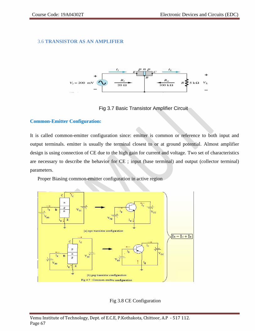
Course Code: 19A04302T Electronic Devices and Circuits (EDC)
Vemu Institute of Technology, Dept. of E.C.E, P.Kothakota, Chittoor, A.P - 517 112. Page 67
3.6 TRANSISTOR AS AN AMPLIFIER
Fig 3.7 Basic Transistor Amplifier Circuit
Common-Emitter Configuration:
It is called common-emitter configuration since: emitter is common or reference to both input and
output terminals. emitter is usually the terminal closest to or at ground potential. Almost amplifier
design is using connection of CE due to the high gain for current and voltage. Two set of characteristics
are necessary to describe the behavior for CE ; input (base terminal) and output (collector terminal)
parameters.
Proper Biasing common-emitter configuration in active region
Fig 3.8 CE Configuration

Course Code: 19A04302T Electronic Devices and Circuits (EDC)
Vemu Institute of Technology, Dept. of E.C.E, P.Kothakota, Chittoor, A.P - 517 112. Page 68
IB is microamperes compared to miliamperes of IC.
IB will flow when VBE > 0.7V for silicon and 0.3V for germanium
Before this value IB is very small and no IB.
Base-emitter junction is forward bias Increasing VCE will reduce IB for different values.
Fig 3.9a Input characteristics for common-emitter npn transistor
Fig 3.9b Output characteristics for common-emitter npn transistor
Beta (β) or amplification factor

Course Code: 19A04302T Electronic Devices and Circuits (EDC)
Vemu Institute of Technology, Dept. of E.C.E, P.Kothakota, Chittoor, A.P - 517 112. Page 69
The ratio of dc collector current (IC) to the dc base current (IB) is dc beta (βdc ) which is dc current gain
where IC and IB are determined at a particular operating point, Q-point (quiescent point). It’s define by
the following equation:
30 < βdc < 300 0 2N3904
On data sheet, βdc=hfe with h is derived from ac hybrid equivalent cct. FE are derived from forward-
current amplification and common-emitter configuration respectively.
For ac conditions, an ac beta has been defined as the changes of collector current (IC) compared to the
changes of base current (IB) where IC and IB are determined at operating point. On data sheet, ac=hfe It
can defined by the following equation:

Course Code: 19A04302T Electronic Devices and Circuits (EDC)
Vemu Institute of Technology, Dept. of E.C.E, P.Kothakota, Chittoor, A.P - 517 112. Page 70
3.7 COMMON – COLLECTOR CONFIGURATION
Also called emitter-follower (EF). It is called common-emitter configuration since both the signal
source and the load share the collector terminal as a common connection point. The output voltage is
obtained at emitter terminal. The input characteristic of common-collector configuration is similar with
common-emitter. Configuration.Common-collector circuit configuration is provided with the load
resistor connected from emitter to ground. It is used primarily for impedance-matching purpose since it
has high input impedance and low output impedance.
Fig 3.10 CC Configuration
For the common-collector configuration, the output characteristics are a plot of IE vs VCE for a
range of values of IB.
Fig 3.11 Output Characteristics of CC Configuration for npn Transistor

Course Code: 19A04302T Electronic Devices and Circuits (EDC)
Vemu Institute of Technology, Dept. of E.C.E, P.Kothakota, Chittoor, A.P - 517 112. Page 71
Field Effect Transistor (FET) 3.1.1 INTRODUCTION
1. The Field effect transistor is abbreviated as FET, it is an semiconductor device like a BJT which
can be used as an amplifier or switch.
2. The Field effect transistor is a voltage operated device. Whereas Bipolar junction transistor is a
current controlled device. Unlike BJT a FET requires virtually no input current.
3. This gives it an extremely high input resistance , which is its most important advantage over a
bipolar transistor.
4. FET is also a three terminal device, labeled as source, drain and gate.
5. The source can be viewed as BJT’s emitter, the drain as collector, and the gate as the counter part
of the base.
6. The material that connects the source to drain is referred to as the channel.
7. FET operation depends only on the flow of majority carriers ,therefore they are called uni polar
devices. BJT operation depends on both minority and majority carriers.
8. As FET has conduction through only majority carriers it is less noisy than BJT.
9. FETs are much easier to fabricate and are particularly suitable for ICs because they occupy less
space than BJTs.
10. FET amplifiers have low gain bandwidth product due to the junction capacitive effects and
produce more signal distortion except for small signal operation.
11. The performance of FET is relatively unaffected by ambient temperature changes. As it has a
negative temperature coefficient at high current levels, it prevents the FET from thermal
breakdown. The BJT has a positive temperature coefficient at high current levels which leads to
thermal breakdown.
3.1.2 CLASSIFICATION OF FET:
There are two major categories of field effect transistors:
1. Junction Field Effect Transistors
2. MOSFETs
These are further sub divided in to P- channel and N-channel devices.
MOSFETs are further classified in to two types Depletion MOSFETs and Enhancement .
MOSFETs When the channel is of N-type the JFET is referred to as an N-channel JFET ,when the
channel is of P-type the JFET is referred to as P-channel JFET.

Course Code: 19A04302T Electronic Devices and Circuits (EDC)
Vemu Institute of Technology, Dept. of E.C.E, P.Kothakota, Chittoor, A.P - 517 112. Page 72
The schematic symbols for the P-channel and N-channel JFETs are shown in the figure.
Fig 5.1 schematic symbols for the P-channel and N-channel JFET
3.1.3 CONSTRUCTION AND OPERATION OF N- CHANNEL FET
If the gate is an N-type material, the channel must be a P-type material.
CONSTRUCTION OF N-CHANNEL JFET
Fig 5.2 Construction of N-Channel JFET
A piece of N- type material, referred to as channel has two smaller pieces of P-type material attached
to its sides, forming PN junctions. The channel ends are designated as the drain and source. And the two
pieces of P-type material are connected together and their terminal is called the gate. Since this channel
is in the N-type bar, the FET is known as N-channel JFET.
OPERATION OF N-CHANNEL JFET:-
The overall operation of the JFET is based on varying the width of the channel to control the drain
current.

Course Code: 19A04302T Electronic Devices and Circuits (EDC)
Vemu Institute of Technology, Dept. of E.C.E, P.Kothakota, Chittoor, A.P - 517 112. Page 73
A piece of N type material referred to as the channel, has two smaller pieces of P type
material attached to its sites, farming PN –Junctions. The channel’s ends are designated the drain and the
source. And the two pieces of P type material are connected together and their terminal is called the
gate. With the gate terminal not connected and the potential applied positive at the drain negative at the
source a drain current Id flows. When the gate is biased negative with respective to the source the PN
junctions are reverse biased and depletion regions are formed.
The channel is more lightly doped than the P type gate blocks, so the depletion regions
penetrate deeply into the channel. Since depletion region is a region depleted of charge carriers it
behaves as an Insulator. The result is that the channel is narrowed. Its resistance is increased and Id is
reduced. When the negative gate bias voltage is further increased, the depletion regions meet at the
center and Id is cut off completely.
There are two ways to control the channel width
1. By varying the value of Vgs
2. And by Varying the value of Vds holding Vgs constant
1. By varying the value of Vgs :-
We can vary the width of the channel and in turn vary the amount of drain current. This can be
done by varying the value of Vgs. This point is illustrated in the fig below. Here we are dealing with N
channel FET. So channel is of N type and gate is of P type that constitutes a PN junction. This PN
junction is always reverse biased in JFET operation .The reverse bias is applied by a battery voltage Vgs
connected between the gate and the source terminal i.e positive terminal of the battery is connected to
the source and negative terminal to gate.

Course Code: 19A04302T Electronic Devices and Circuits (EDC)
Vemu Institute of Technology, Dept. of E.C.E, P.Kothakota, Chittoor, A.P - 517 112. Page 74
1) When a PN junction is reverse biased the electrons and holes diffuse across junction by leaving
immobile ions on the N and P sides , the region containing these immobile ions is known as
depletion regions.
2) If both P and N regions are heavily doped then the depletion region extends symmetrically on
both sides.
3) But in N channel FET P region is heavily doped than N type thus depletion region extends more
in N region than P region.
4) So when no Vds is applied the depletion region is symmetrical and the conductivity becomes
Zero. Since there are no mobile carriers in the junction.
5) As the reverse bias voltage is increases the thickness of the depletion region also increases. i.e.
the effective channel width decreases .
6) By varying the value of Vgs we can vary the width of the channel.
2. Varying the value of Vds holding Vgs constant :-
1) When no voltage is applied to the gate i.e. Vgs=0 , Vds is applied between source and drain the
electrons will flow from source to drain through the channel constituting drain current Id .
2) With Vgs= 0 for Id= 0 the channel between the gate junctions is entirely open .In response to a
small applied voltage Vds , the entire bar acts as a simple semi conductor resistor and the current
Id increases linearly with Vds .
3) The channel resistances are represented as rd and rs as shown in the fig.

Course Code: 19A04302T Electronic Devices and Circuits (EDC)
Vemu Institute of Technology, Dept. of E.C.E, P.Kothakota, Chittoor, A.P - 517 112. Page 75
4) This increasing drain current Id produces a voltage drop across rd which reverse biases the gate
to source junction,(rd> rs) .Thus the depletion region is formed which is not symmetrical .
5) The depletion region i.e. developed penetrates deeper in to the channel near drain and less
towards source because Vrd >> Vrs. So reverse bias is higher near drain than at source.
6) As a result growing depletion region reduces the effective width of the channel. Eventually a
voltage Vds is reached at which the channel is pinched off. This is the voltage where the current
Id begins to level off and approach a constant value.
So, by varying the value of Vds we can vary the width of the channel holding Vgs constant.
When both Vgs and Vds is applied:-
It is of course in principle not possible for the channel to close Completely and there by reduce the
current Id to Zero for, if such indeed, could be the case the gate voltage Vgs is applied in the direction to
provide additional reverse bias
1) When voltage is applied between the drain and source with a battery Vdd, the electrons flow
from source to drain through the narrow channel existing between the depletion regions. This
constitutes the drain current Id, its conventional direction is from drain to source.
2) The value of drain current is maximum when no external voltage is applied between gate and
source and is designated by Idss.

Course Code: 19A04302T Electronic Devices and Circuits (EDC)
Vemu Institute of Technology, Dept. of E.C.E, P.Kothakota, Chittoor, A.P - 517 112. Page 76
3) When Vgs is increased beyond Zero the depletion regions are widened. This reduces the
effective width of the channel and therefore controls the flow of drain current through the
channel.
4) When Vgs is further increased a stage is reached at which to depletion regions touch each other
that means the entire channel is closed with depletion region. This reduces the drain current to
Zero.
5.4 CHARACTERISTICS OF N-CHANNEL JFET
The family of curves that shows the relation between current and voltage are known as
characteristic curves.
There are two important characteristics of a JFET.
1) Drain or VI Characteristics
2) Transfer characteristics
1. Drain Characteristics:-
Drain characteristics shows the relation between the drain to source voltage Vds and drain current Id.
In order to explain typical drain characteristics let us consider the curve with Vgs= 0.V.
1) When Vds is applied and it is increasing the drain current ID also increases linearly up to knee
point.
2) This shows that FET behaves like an ordinary resistor.This region is called as ohmic region.
3) ID increases with increase in drain to source voltage. Here the drain current is increased slowly
as compared to ohmic region.

Course Code: 19A04302T Electronic Devices and Circuits (EDC)
Vemu Institute of Technology, Dept. of E.C.E, P.Kothakota, Chittoor, A.P - 517 112. Page 77
4) It is because of the fact that there is an increase in VDS .This in turn increases the reverse bias
voltage across the gate source junction .As a result of this depletion region grows in size thereby
reducing the effective width of the channel.
5) All the drain to source voltage corresponding to point the channel width is reduced to a
minimum value and is known as pinch off.
5) The drain to source voltage at which channel pinch off occurs is called pinch off voltage(Vp).
PINCH OFF Region:-
1) This is the region shown by the curve as saturation region.
2) It is also called as saturation region or constant current region. Because of the channel is
occupied with depletion region , the depletion region is more towards the drain and less
towards the source, so the channel is limited, with this only limited number of carriers are
only allowed to cross this channel from source drain causing a current that is constant in this
region. To use FET as an amplifier it is operated in this saturation region.
3) In this drain current remains constant at its maximum value IDSS.
4) The drain current in the pinch off region depends upon the gate to source voltage and is given
by the relation
Id =Idss [1-Vgs/Vp]2
This is known as shokley’s relation.
BREAKDOWN REGION:-
1) The region is shown by the curve .In this region, the drain current increases rapidly as the
drain to source voltage is increased.
2) It is because of the gate to source junction due to avalanche effect.
3) The avalanche break down occurs at progressively lower value of VDS because the reverse
bias gate voltage adds to the drain voltage thereby increasing effective voltage across the gate
junction
This causes
1. The maximum saturation drain current is smaller
2. The ohmic region portion decreased.
4) It is important to note that the maximum voltage VDS which can be applied to FET is the lowest
voltage which causes available break down.

Course Code: 19A04302T Electronic Devices and Circuits (EDC)
Vemu Institute of Technology, Dept. of E.C.E, P.Kothakota, Chittoor, A.P - 517 112. Page 78
3.1.3 TRANSFER CHARACTERISTICS:-
These curves shows the relationship between drain current ID and gate to source voltage
VGS for different values of VDS.
1) First adjust the drain to source voltage to some suitable value , then increase the gate to
source voltage in small suitable value.
2) Plot the graph between gate to source voltage along the horizontal axis and current ID on
the vertical axis. We shall obtain a curve like this.
3) As we know that if Vgs is more negative curves drain current to reduce . where Vgs is made
sufficiently negative, Id is reduced to zero. This is caused by the widening of the depletion region to a
point where it is completely closes the channel. The value of Vgs at the cutoff point is designed as Vgsoff
The upper end of the curve as shown by the drain current value is equal to Idss that is when Vgs = 0 the
drain current is maximum.
While the lower end is indicated by a voltage equal to Vgsoff
4) If Vgs continuously increasing , the channel width is reduced , then Id =0
It may be noted that curve is part of the parabola; it may be expressed as Id=Idss[1-Vgs/Vgsoff]2

Course Code: 19A04302T Electronic Devices and Circuits (EDC)
Vemu Institute of Technology, Dept. of E.C.E, P.Kothakota, Chittoor, A.P - 517 112. Page 79
Why the gate to source junction of a JFET be always reverse biased ?
The gate to source junction of a JFET is never allowed to become forward biased because
the gate material is not designed to handle any significant amount of current. If the junction is allowed to
become forward biased, current is generated through the gate material. This current may destroy the
component.
There is one more important characteristic of JFET reverse biasing i.e. J FET ‘s have extremely
high characteristic gate input impedance. This impedance is typically in the high mega ohm range. With
the advantage of extremely high input impedance it draws no current from the source. The high input
impedance of the JFET has led to its extensive use in integrated circuits. The low current requirements
of the component makes it perfect for use in ICs. Where thousands of transistors must be etched on to a
single piece of silicon. The low current draw helps the IC to remain relatively cool, thus allowing more
components to be placed in a smaller physical area.
3.1.4 JFET PARAMETERS
The electrical behavior of JFET may be described in terms of certain parameters. Such
parameters are obtained from the characteristic curves.
A C Drain resistance(rd):
It is also called dynamic drain resistance and is the a.c. resistance between the drain and source terminal,
when the JFET is operating in the pinch off or saturation region. It is given by the ratio of small change
in drain to source voltage ∆Vds to the corresponding change in drain current ∆Id for a constant gate to
source voltage Vgs.
Mathematically it is expressed as rd=∆Vds/ ∆Id where Vgs is held constant.
Trance Conductance (gm):
It is also called forward transconductance . It is given by the ratio of small change in drain current (∆Id)
to the corresponding change in gate to source voltage (∆Vds)
Mathematically the transconductance can be written as
gm=∆Id/∆Vds
AMPLIFICATION FACTOR (µ)

Course Code: 19A04302T Electronic Devices and Circuits (EDC)
Vemu Institute of Technology, Dept. of E.C.E, P.Kothakota, Chittoor, A.P - 517 112. Page 80
It is given by the ratio of small change in drain to source voltage (∆Vds) to the corresponding change in
gate to source voltage (∆Vgs)for a constant drain current (Id).
Thus µ=∆Vds/∆Vgs when Id held constant
The amplification factor µ may be expressed as a product of transconductance (gm)and ac drain resistance (rd) µ=∆Vds/∆Vgs=gm rd
3.1.5 THE FET SMALL SIGNAL MODEL
The linear small signal equivalent circuit for the FET can be obtained in a manner similar to that used to derive the corresponding model for a transistor.
We can express the drain current iD as a function f of the gate voltage and drain voltage Vds.
Id =f(Vgs,Vds)---------------- (1)
rd= |Vgs
The reciprocal of the rd is the drain conductance gd .It is also designated by Yos and Gos and
called the common source output conductance . So the small signal equivalent circuit for FET can be
drawn in two different ways.
1.small signal current –source model
2.small signal voltage-source model.
A small signal current –source model for FET in common source configuration can be drawn satisfying Eq→(1) as shown in the figure(a)
This low frequency model for FET has a Norton’s output circuit with a dependent current
generator whose magnitude is proportional to the gate-to –source voltage. The proportionality factor is
the transconductance ‘gm’. The output resistance is ‘rd’. The input resistance between the gate and source
is infinite, since it is assumed that the reverse biased gate draws no current. For the same reason the
resistance between gate and drain is assumed to be infinite.
The small signal voltage-source model is shown in the figure(b).
This can be derived by finding the Thevenin’s equivalent for the output part of fig(a) .

Course Code: 19A04302T Electronic Devices and Circuits (EDC)
Vemu Institute of Technology, Dept. of E.C.E, P.Kothakota, Chittoor, A.P - 517 112. Page 81
These small signal models for FET can be used for analyzing the three basic FET amplifier configurations:
1. Common source (CS)
2. Common drain (CD) or source follower
3. Common gate(CG).
(a)Small Signal Current source model for FET (b)Small Signal voltage source model for FET
Here the input circuit is kept open because of having high input impedance and the output
circuit satisfies the equation for ID.
3.1.6 MOSFET
We now turn our attention to the insulated gate FET or metal oxide semi conductor FET which is
having the greater commercial importance than the junction FET.Most MOSFETS however are triodes,
with the substrate internally connected to the source. The circuit symbols used by several manufacturers
are indicated in the Fig below.
(a) Depletion type MOSFET (b) Enhancement type MOSFET
Here are two basic types of MOSFETS
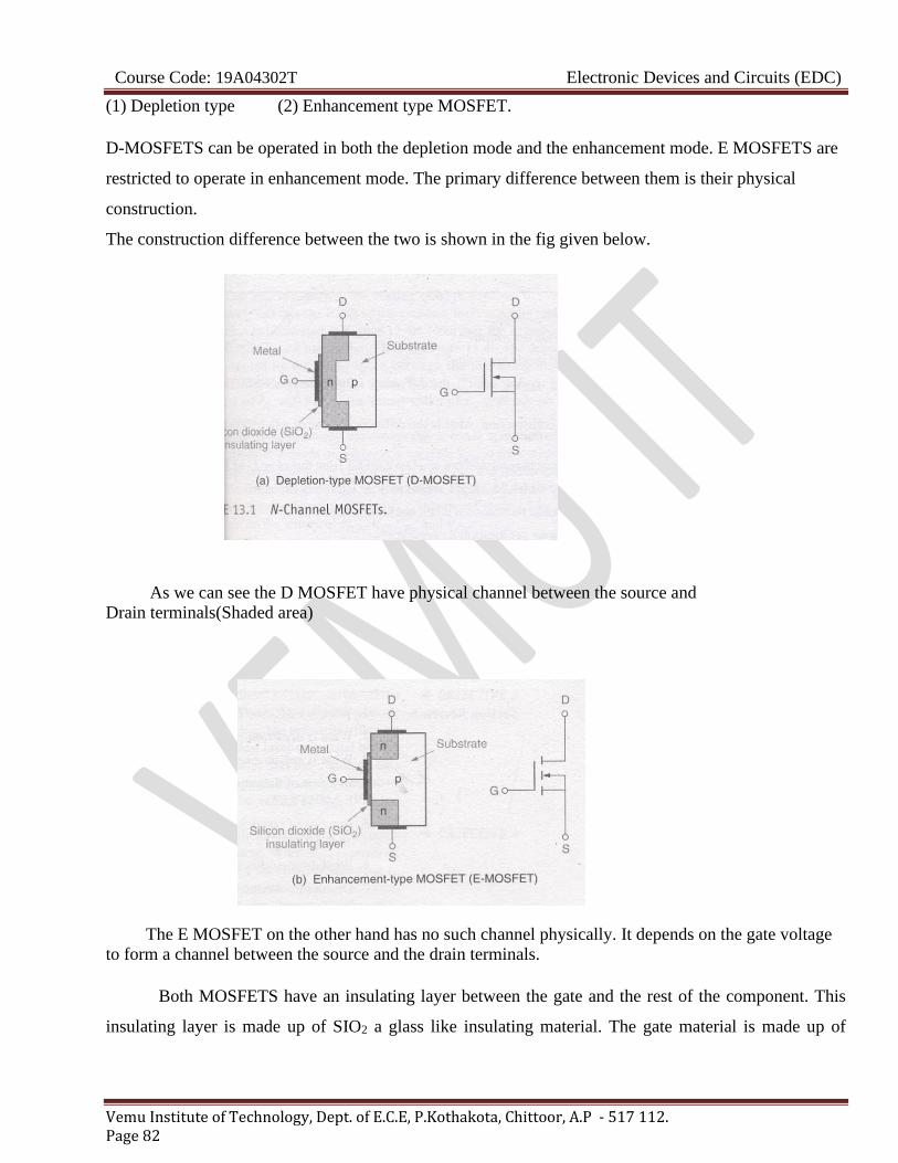
Course Code: 19A04302T Electronic Devices and Circuits (EDC)
Vemu Institute of Technology, Dept. of E.C.E, P.Kothakota, Chittoor, A.P - 517 112. Page 82
(1) Depletion type (2) Enhancement type MOSFET.
D-MOSFETS can be operated in both the depletion mode and the enhancement mode. E MOSFETS are
restricted to operate in enhancement mode. The primary difference between them is their physical
construction.
The construction difference between the two is shown in the fig given below.
As we can see the D MOSFET have physical channel between the source and Drain terminals(Shaded area)
The E MOSFET on the other hand has no such channel physically. It depends on the gate voltage to form a channel between the source and the drain terminals.
Both MOSFETS have an insulating layer between the gate and the rest of the component. This
insulating layer is made up of SIO2 a glass like insulating material. The gate material is made up of

Course Code: 19A04302T Electronic Devices and Circuits (EDC)
Vemu Institute of Technology, Dept. of E.C.E, P.Kothakota, Chittoor, A.P - 517 112. Page 83
metal conductor .Thus going from gate to substrate, we can have metal oxide semi conductor which is
where the term MOSFET comes from.
Since the gate is insulated from the rest of the component, the MOSFET is sometimes referred to
as an insulated gate FET or IGFET. The foundation of the MOSFET is called the substrate. This
material is represented in the schematic symbol by the center line that is connected to the source.
In the symbol for the MOSFET, the arrow is placed on the substrate. As with JFET an arrow
pointing in represents an N-channel device, while an arrow pointing out represents p-channel device.
CONSTRUCTION OF AN N-CHANNEL MOSFET:-
The N- channel MOSFET consists of a lightly doped p type substance into which two heavily
doped n+ regions are diffused as shown in the Fig. These n+ sections , which will act as source and
drain.
A thin layer of insulation silicon dioxide (SIO2) is grown over the surface of the structure, and
holes are cut into oxide layer, allowing contact with the source and drain. Then the gate metal area is
overlaid on the oxide, covering the entire channel region.Metal contacts are made to drain and source
and the contact to the metal over the channel area is the gate terminal.The metal area of the gate, in
conjunction with the insulating dielectric oxide layer and the semiconductor channel, forms a parallel
plate capacitor. The insulating layer of sio2.
3.1.7 DEPLETION MOSFET
The basic structure of D –MOSFET is shown in the fig. An N-channel is diffused between source
and drain with the device an appreciable drain current IDSS flows foe zero gate to source voltage,
Vgs=0.

Course Code: 19A04302T Electronic Devices and Circuits (EDC)
Vemu Institute of Technology, Dept. of E.C.E, P.Kothakota, Chittoor, A.P - 517 112. Page 84
Depletion mode operation:-
1) The above fig shows the D-MOSFET operating conditions with gate and source terminals shorted
together(VGS=0V)
2) At this stage ID= IDSS where VGS=0V, with this voltage VDS, an appreciable drain current
IDSS flows.
3) If the gate to source voltage is made negative i.e. VGs is negative .Positive charges are induced in
the channel through the SIO2 of the gate capacitor.
4) Since the current in a FET is due to majority carriers(electrons for an N-type material) , the
induced positive charges make the channel less conductive and the drain current drops as Vgs is
made more negative.
5) The re distribution of charge in the channel causes an effective depletion of majority carriers ,
which accounts for the designation depletion MOSFET.
6) That means biasing voltage Vgs depletes the channel of free carriers This effectively reduces the
width of the channel , increasing its resistance.
7) Note that negative Vgs has the same effect on the MOSFET as it has on the JFET.
8) As shown in the fig above, the depletion layer generated by Vgs (represented by the white space
between the insulating material and the channel) cuts into the channel, reducing its width. As a
result ,Id<Idss.The actual value of ID depends on the value of Idss,Vgs(off) and Vgs.
Enhancement mode operation of the D-MOSFET:-
1) This operating mode is a result of applying a positive gate to source voltage Vgs to the device.
2) When Vgs is positive the channel is effectively widened. This reduces the resistance of the
channel allowing ID to exceed the value of IDSS
3) When Vgs is given positive the majority carriers in the p-type are holes. The holes in the p type
substrate are repelled by the +ve gate voltage.

Course Code: 19A04302T Electronic Devices and Circuits (EDC)
Vemu Institute of Technology, Dept. of E.C.E, P.Kothakota, Chittoor, A.P - 517 112. Page 85
4) At the same time, the conduction band electrons (minority carriers) in the p type material are
attracted towards the channel by the +gate voltage.
5) With the build up of electrons near the channel , the area to the right of the physical channel
effectively becomes an N type material.
6) The extended n type channel now allows more current, Id> Idss
Characteristics of Depletion MOSFET:- The fig. shows the drain characteristics for the N channel depletion type MOSFET
1) The curves are plotted for both Vgs positive and Vgs negative voltages
.When Vgs=0 and negative the MOSFET operates in depletion mode when Vgs is positive ,the
MOSFET operates in the enhancement mode.
2) The difference between JFET and D MOSFET is that JFET does not operate for positive values
of Vgs.
3) When Vds=0, there is no conduction takes place between source to drain, if Vgs<0 and Vds>0
then Id increases linearly.
4) But as Vgs,0 induces positive charges holes in the channel, and controls the channel width. Thus
the conduction between source to drain is maintained as constant, i.e. Id is constant.
5) If Vgs>0 the gate induces more electrons in channel side, it is added with the free electrons
generated by source. again the potential applied to gate determines the channel width and
maintains constant current flow through it as shown in Fig

Course Code: 19A04302T Electronic Devices and Circuits (EDC)
Vemu Institute of Technology, Dept. of E.C.E, P.Kothakota, Chittoor, A.P - 517 112. Page 86
TRANSFER CHARACTERISTICS:-
The combination of 3 operating states i.e. Vgs=0V, VGs<0V, Vgs>0V is represented by the
DMOSFET trans conductance curve shown in Fig.
1) Here in this curve it may be noted that the region AB of the characteristics similar to that of
JFET.
2) This curve extends for the positive values of Vgs
3) Note that Id=Idss for Vgs=0V when Vgs is negative,Id< Idss when Vgs= Vgs(off) ,Id is reduced
to approximately omA.Where Vgs is positive Id>Idss.So obviously Idss is not the maximum
possible value of Id for a MOSFET.
4) The curves are similar to JFET so thet the D MOSFET have the same transconductance equation.
3.1.8 E-MOSFETS
The E MOSFET is capable of operating only in the enhancement mode.The gate potential must be
positive w.r.t to source.
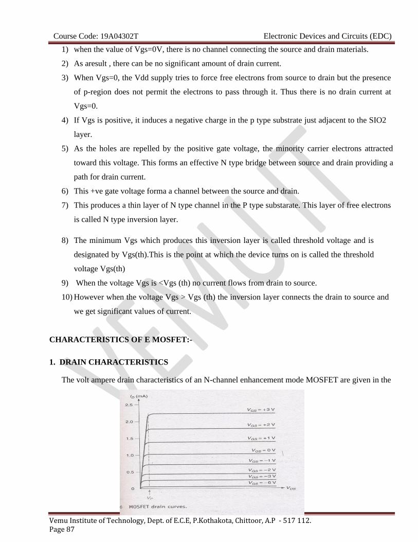
Course Code: 19A04302T Electronic Devices and Circuits (EDC)
Vemu Institute of Technology, Dept. of E.C.E, P.Kothakota, Chittoor, A.P - 517 112. Page 87
1) when the value of Vgs=0V, there is no channel connecting the source and drain materials.
2) As aresult , there can be no significant amount of drain current.
3) When Vgs=0, the Vdd supply tries to force free electrons from source to drain but the presence
of p-region does not permit the electrons to pass through it. Thus there is no drain current at
Vgs=0.
4) If Vgs is positive, it induces a negative charge in the p type substrate just adjacent to the SIO2
layer.
5) As the holes are repelled by the positive gate voltage, the minority carrier electrons attracted
toward this voltage. This forms an effective N type bridge between source and drain providing a
path for drain current.
6) This +ve gate voltage forma a channel between the source and drain.
7) This produces a thin layer of N type channel in the P type substarate. This layer of free electrons
is called N type inversion layer.
8) The minimum Vgs which produces this inversion layer is called threshold voltage and is
designated by Vgs(th).This is the point at which the device turns on is called the threshold
voltage Vgs(th)
9) When the voltage Vgs is <Vgs (th) no current flows from drain to source.
10) However when the voltage Vgs > Vgs (th) the inversion layer connects the drain to source and
we get significant values of current.
CHARACTERISTICS OF E MOSFET:-
1. DRAIN CHARACTERISTICS
The volt ampere drain characteristics of an N-channel enhancement mode MOSFET are given in the

Course Code: 19A04302T Electronic Devices and Circuits (EDC)
Vemu Institute of Technology, Dept. of E.C.E, P.Kothakota, Chittoor, A.P - 517 112. Page 88
2. TRANSFER CHARACTERISTICS:-
1) The current Idss at Vgs≤ 0 is very small beinf of the order of a few nano amps.
2) As Vgs is made +ve , the current Id increases slowly at forst, and then much more rapidly with
an increase in Vgs.
3) The standard transconductance formula will not work for the E MOSFET.
4) To determine the value of ID at a given value of VGs we must use the following relation
Id =K[Vgs-Vgs(Th)]2
Where K is constant for the MOSFET . found as
K=
From the data specification sheets, the 2N7000 has the following ratings.
Id(on)= 75mA(minimum).
And Vgs(th)=0.8(minimum)
3.1.8 APPLICATIONS
One of the primary contributions to electronics made by MOSFETs can beal (computer electronics).
The signals in digital circuits are made up of rapidly switching dc levels. This signal is called as a
rectangular wave ,made up of two dc levels (or logic levels). These logic levels are 0V and +5V.
A group of circuits with similar circuitry and operating characteristics is referred to as a logic family.
All the circuits in a given logic family respond to the same logic levels, have similar speed and power-
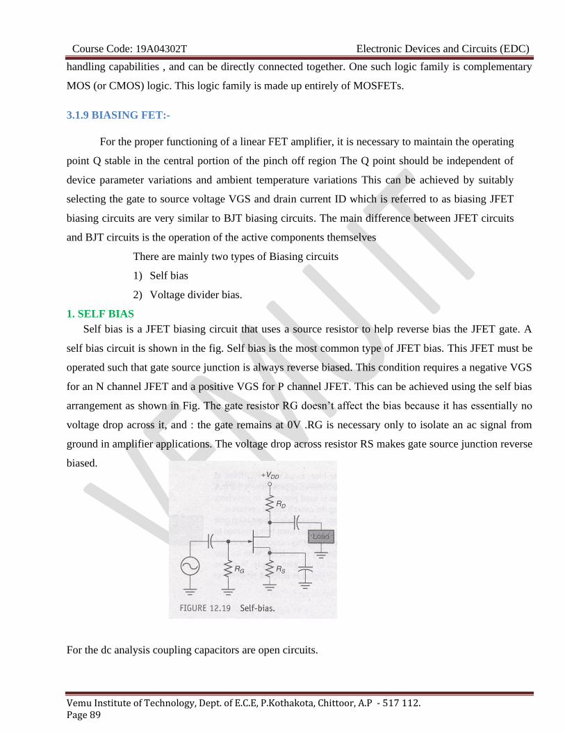
Course Code: 19A04302T Electronic Devices and Circuits (EDC)
Vemu Institute of Technology, Dept. of E.C.E, P.Kothakota, Chittoor, A.P - 517 112. Page 89
handling capabilities , and can be directly connected together. One such logic family is complementary
MOS (or CMOS) logic. This logic family is made up entirely of MOSFETs.
3.1.9 BIASING FET:-
For the proper functioning of a linear FET amplifier, it is necessary to maintain the operating
point Q stable in the central portion of the pinch off region The Q point should be independent of
device parameter variations and ambient temperature variations This can be achieved by suitably
selecting the gate to source voltage VGS and drain current ID which is referred to as biasing JFET
biasing circuits are very similar to BJT biasing circuits. The main difference between JFET circuits
and BJT circuits is the operation of the active components themselves
There are mainly two types of Biasing circuits
1) Self bias
2) Voltage divider bias.
1. SELF BIAS Self bias is a JFET biasing circuit that uses a source resistor to help reverse bias the JFET gate. A
self bias circuit is shown in the fig. Self bias is the most common type of JFET bias. This JFET must be
operated such that gate source junction is always reverse biased. This condition requires a negative VGS
for an N channel JFET and a positive VGS for P channel JFET. This can be achieved using the self bias
arrangement as shown in Fig. The gate resistor RG doesn’t affect the bias because it has essentially no
voltage drop across it, and : the gate remains at 0V .RG is necessary only to isolate an ac signal from
ground in amplifier applications. The voltage drop across resistor RS makes gate source junction reverse
biased.
For the dc analysis coupling capacitors are open circuits.

Course Code: 19A04302T Electronic Devices and Circuits (EDC)
Vemu Institute of Technology, Dept. of E.C.E, P.Kothakota, Chittoor, A.P - 517 112. Page 90
For the N channel FET in Fig (a)
IS produces a voltage drop across RS and makes the source positive w.r.t ground. In any JFET circuit all
the source current passes through the device to the drain circuit .This is due to the fact that there is no
significant gate current.
We can define source current as IS = ID
(VG =0 because there is no gate current flowing in RG So VG across RG is zero)
VG =0 then VS= ISRS =ID RS
VGS = VG-VS =0-ID RS=- ID RS
DC analysis of self Bias:- In the following DC analysis, the N channel J FET shown in the fig. is used for illustration.
For DC analysis we can replace coupling capacitors by open circuits and we can also replace the
resistor RG by a short circuit equivalent.:. IG = 0.The relation between ID and VGS is given by
Vs= Is Rs =IdRs
Vgs=Vg-Vs=0-IdRs=-IdRs Drawing the self bias line:-
Typical transfer characteristics for a self biased JFET are shown in the fig.The maximum drain current is
5mA and the gate source cut off voltage is -3V. This means the gate voltage has to be between 0 and -
3V.

Course Code: 19A04302T Electronic Devices and Circuits (EDC)
Vemu Institute of Technology, Dept. of E.C.E, P.Kothakota, Chittoor, A.P - 517 112. Page 91
Now using the equation VGS = -IDRS and assuming RS of any suitable value we can draw the self bias line.
2. VOLTAGE DIVIDER BIAS:-
The fig. shows N channel JFET with voltage divider bias. The voltage at the source of JFET
must be more positive than the voltage at the gate in order to keep the gate to source junction reverse
biased. The source voltage is
VS = IDRS
The gate voltage is set by resistors R1 and R2 as expressed by the following equation using the
voltage divider formula.
Vg= Vdd
For dc analysis
Applying KVL to the input circuit
VG-VGS-VS =0
:: VGS = VG-VS=VG-ISRS
VGS = VG-ID RS :: IS = ID
Applying KVL to the input circuit we get
VDS+IDRD+VS-VDD =0
VDS = VDD-IDRD-IDRS
VDS = VDD-ID ( RD +RS )

Course Code: 19A04302T Electronic Devices and Circuits (EDC)
Vemu Institute of Technology, Dept. of E.C.E, P.Kothakota, Chittoor, A.P - 517 112. Page 92
The Q point of a JFET amplifier, using the voltage divider bias is
IDQ = IDSS [1-VGS/VP]2
VDSQ = VDD-ID ( RD+RS )
COMPARISON OF MOSFET WITH JFET
a. In enhancement and depletion types of MOSFET, the transverse electric field induced
across an insulating layer deposited on the semiconductor material controls the
conductivity of the channel.
b. In the JFET the transverse electric field across the reverse biased PN junction controls the
conductivity of the channel.
c. The gate leakage current in a MOSFET is of the order of 10-12A. Hence the input resistance
of a MOSFET is very high in the order of 1010 to 1015 Ω. The gate leakage current of a
JFET is of the order of 10-9A., and its input resistance is of the order of 108Ω.
d. The output characteristics of the JFET are flatter than those of the MOSFET, and hence the
drain resistance of a JFET (0.1 to 1MΩ) is much higher than that of a MOSFET (1 to
50kΩ).
e. JFETs are operated only in the depletion mode. The depletion type MOSFET may
be operated in both depletion and enhancement mode.
f. Comparing to JFET, MOSFETs are easier to fabricate.
g. Special digital CMOS circuits are available which involve near zero power dissipation
and very low voltage and current requirements. This makes them suitable for portable
systems.

Course Code: 19A04302T Electronic Devices and Circuits (EDC)
Vemu Institute of Technology, Dept. of E.C.E, P.Kothakota, Chittoor, A.P - 517 112. Page 93
UNIT-IV
TRANSISTOR BIASING AND STABILIZATION 4.1 NEED FOR TRANSISTOR BIASING
If the o/p signal must be a faithful reproduction of the i/p signal, the transistor must be operated
in active region. That means an operating point has to be established in this region . To establish an
operating point (proper values of collector current Ic and collector to emitter voltage VCE) appropriate
supply voltages and resistances must be suitably chosen in the ckt. This process of selecting proper
supply voltages and resistance for obtaining desired operating point or Q point is called as biasing and
the ckt used for transistor biasing is called as biasing ckt.
There are four conditions to be met by a transistor so that it acts as a faithful amplification:
1) Emitter base junction must be forward biased (VBE=0.7Vfor Si, 0.2V for Ge) and collector base
junction must be reverse biased for all levels of i/p signal.
2) Vce voltage should not fall below VCE (sat) (0.3V for Si, 0.1V for Ge) for any part of the i/p signal.
For VCE less than VCE (sat) the collector base junction is not probably reverse biased.
3) The value of the signal Ic when no signal is applied should be at least equal to the max. collector
current t due to signal alone.
4) Max. rating of the transistor Ic(max), VCE (max) and PD(max) should not be exceeded at any value of
i/p signal.
Consider the fig shown in fig1. If operating point is selected at A, A represents a condition when no
bias is applied to the transistor i.e, Ic=0, VCE =0. It does not satisfy the above said conditions necessary
for faithful amplification.
Point C is too close to PD(max) curve of the transistor. Therefore the o/p voltage swing in the positive
direction is limited.
Point B is located in the middle of active region .It will allow both positive and negative half cycles
in the o/p signal. It also provides linear gain and larger possible o/p voltages and currents. Hence
operating point for a transistor amplifier is selected to be in the middle of active region.

Course Code: 19A04302T Electronic Devices and Circuits (EDC)
Vemu Institute of Technology, Dept. of E.C.E, P.Kothakota, Chittoor, A.P - 517 112. Page 94
Fig 4.1CE Output Characteristics 4.2 DC LOAD LINE
Referring to the biasing circuit of fig 4.2a, the values of VCC and RC are fixed and Ic and VCE are dependent on RB.
Applying Kirchhoff’s voltage law to the collector circuit in fig. 4.2a, we get
Fig 4.2a CE Amplifier circuit (b) Load line

Course Code: 19A04302T Electronic Devices and Circuits (EDC)
Vemu Institute of Technology, Dept. of E.C.E, P.Kothakota, Chittoor, A.P - 517 112. Page 95
The straight line represented by AB in fig4.2b is called the dc load line. The coordinates of the end
point A are obtained by substituting VCE =0 in the above equation. Then . Therefore The
coordinates of A are VCE =0 and .
The coordinates of B are obtained by substituting Ic=0 in the above equation. Then Vce = Vcc.
Therefore the coordinates of B are VCE =Vcc and Ic=0. Thus the dc load line AB can be drawn if the
values of Rc and Vcc are known.
As shown in the fig4.2b, the optimum point is located at the mid point of the midway between a and
b. In order to get faithful amplification, the Q point must be well within the active region of the
transistor.
Even though the Q point is fixed properly, it is very important to ensure that the operating point
remains stable where it is originally fixed. If the Q point shifts nearer to either A or B, the output voltage
and current get clipped, thereby o/p signal is distorted.
In practice, the Q-point tends to shift its position due to any or all of the following three main
factors.
1) Reverse saturation current, Ico, which doubles for every 10oC raise in temperature
2) Base emitter Voltage ,VBE, which decreases by 2.5 mV per oC
3) Transistor current gain, hFE or β which increases with temperature.
If base current IB is kept constant since IB is approximately equal to Vcc/RB. If the transistor is
replaced by another one of the same type, one cannot ensure that the new transistor will have identical
parameters as that of the first one. Parameters such as β vary over a range. This results in the variation of
collector current Ic for a given IB. Hence , in the o/p characteristics, the spacing between the curves
might increase or decrease which leads to the shifting of the Q-point to a location which might be
completely unsatisfactory.
4.3 AC LOAD LINE
After drawing the dc load line, the operating point Q is properly located at the center of the dc
load line. This operating point is chosen under zero input signal condition of the circuit. Hence the ac
load line should also pas through the operating point Q. The effective ac load resistance Rac, is a
combination of RC parallel to RL i.e. || . So the slope of the ac load line CQD will be .
To draw the ac load line, two end points, I.e. VCE(max) and IC(max) when the signal is applied are required.

Course Code: 19A04302T Electronic Devices and Circuits (EDC)
Vemu Institute of Technology, Dept. of E.C.E, P.Kothakota, Chittoor, A.P - 517 112. Page 96
By joining points c and D, ac load line CD is constructed. As RC > Rac, The dc load line is less steep than ac load line.
4.4 STABILITY FACTOR (S):
The rise of temperature results in increase in the value of transistor gain β and the leakage
current Ico. So, IC also increases which results in a shift in operating point. Therefore, The biasing
network should be provided with thermal stability. Maintenance of the operating point is specified by S,
which indicates the degree of change in operating point due to change in temperature.
The extent to which IC is stabilized with varying IC is measured by a stability factor S
,
For CE configuration
Differentiate the above equation w.r.t IC , We get
S should be small to have better thermal stability.
Stability factor S’ and S’’:
S’ is defined as the rate of change of IC with VBE, keeping IC and VBE constant.
S’’ is defined as the rate of change of IC with β, keeping ICO and VBE constant.
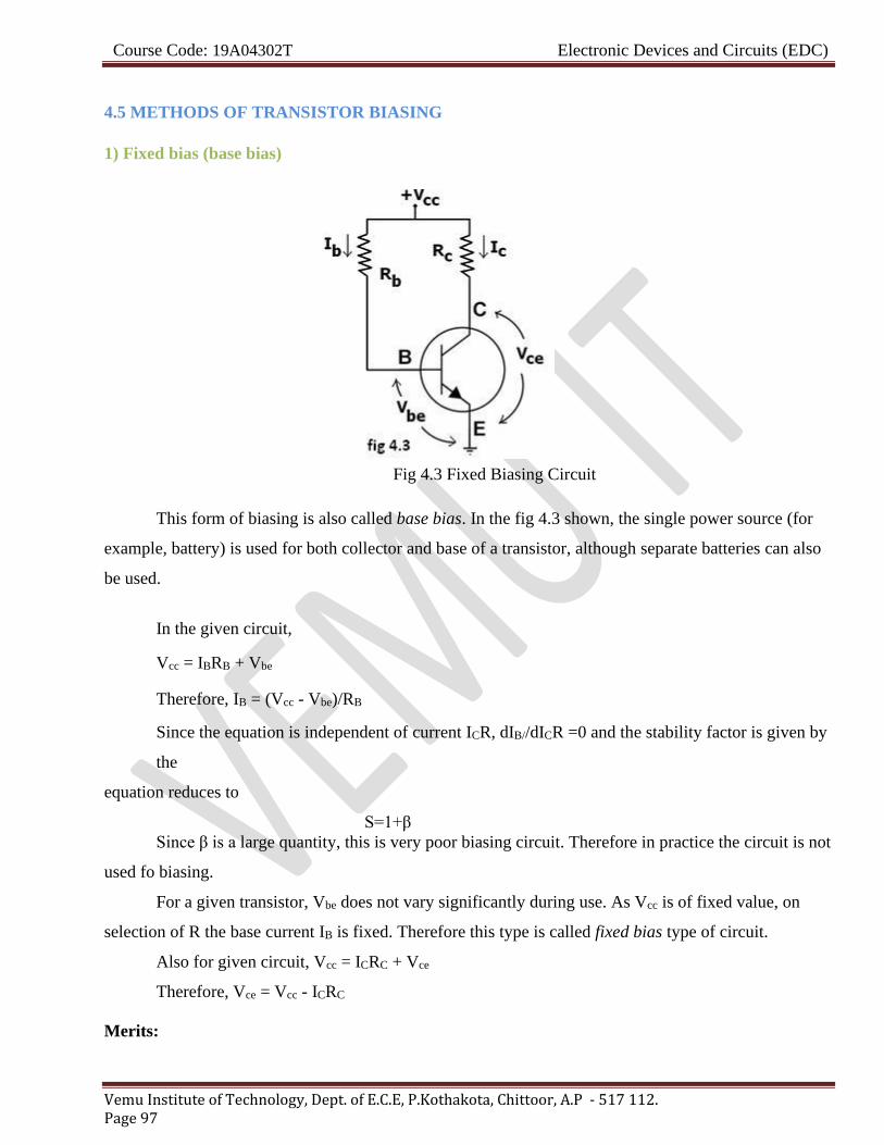
Course Code: 19A04302T Electronic Devices and Circuits (EDC)
Vemu Institute of Technology, Dept. of E.C.E, P.Kothakota, Chittoor, A.P - 517 112. Page 97
4.5 METHODS OF TRANSISTOR BIASING
1) Fixed bias (base bias)
Fig 4.3 Fixed Biasing Circuit
This form of biasing is also called base bias. In the fig 4.3 shown, the single power source (for
example, battery) is used for both collector and base of a transistor, although separate batteries can also
be used.
In the given circuit,
Vcc = IBRB + Vbe
Therefore, IB = (Vcc - Vbe)/RB
Since the equation is independent of current ICR, dIB//dICR =0 and the stability factor is given by
the
equation reduces to
S=1+β
Since β is a large quantity, this is very poor biasing circuit. Therefore in practice the circuit is not
used fo biasing.
For a given transistor, Vbe does not vary significantly during use. As Vcc is of fixed value, on
selection of R the base current IB is fixed. Therefore this type is called fixed bias type of circuit.
Also for given circuit, Vcc = ICRC + Vce
Therefore, Vce = Vcc - ICRC
Merits:

Course Code: 19A04302T Electronic Devices and Circuits (EDC)
Vemu Institute of Technology, Dept. of E.C.E, P.Kothakota, Chittoor, A.P - 517 112. Page 98
• It is simple to shift the operating point anywhere in the active region by merely changing the
base resistor (RB).
• A very small number of components are required.
Demerits:
• The collector current does not remain constant with variation in temperature or power supply
voltage. Therefore the operating point is unstable.
• Changes in Vbe will change IB and thus cause RE to change. This in turn will alter the gain of the
stage.
• When the transistor is replaced with another one, considerable change in the value of β can be
expected. Due to this change the operating point will shift.
1) EMITTER-FEEDBACK BIAS:
The emitter feedback bias circuit is shown in the fig 4.4. The fixed bias circuit is modified by
attaching an external resistor to the emitter. This resistor introduces negative feedback that stabilizes
the Q-point. From Kirchhoff's voltage law, the voltage across the base resistor is
VRb = VCC - IeRe - Vbe.
Fig 4.4 Self Biasing Circuit
From Ohm's law, the base current is
Ib = VRb / Rb.
The way feedback controls the bias point is as follows. If Vbe is held constant and temperature
increases, emitter current increases. However, a larger Ie increases the emitter voltage Ve = IeRe, which
in turn reduces the voltage VRb across the base resistor. A lower base-resistor voltage drop reduces the
base current, which results in less collector current because Ic = ß IB. Collector current and emitter
current are related by Ic = α Ie with α ≈ 1, so increase in emitter current with temperature is opposed,
and operating point is kept stable.

Course Code: 19A04302T Electronic Devices and Circuits (EDC)
Vemu Institute of Technology, Dept. of E.C.E, P.Kothakota, Chittoor, A.P - 517 112. Page 99
Similarly, if the transistor is replaced by another, there may be a change in IC (corresponding to
change in β-value, for example). By similar process as above, the change is negated and operating
point kept stable.
For the given circuit,
IB = (VCC - Vbe)/(RB + (β+1)RE).
Merits:
The circuit has the tendency to stabilize operating point against changes in temperature and β-
value.
Demerits:
• In this circuit, to keep IC independent of β the following condition must be met:
which is approximately the case if ( β + 1 )RE >> RB.
• As β-value is fixed for a given transistor, this relation can be satisfied either by keeping RE
very large, or making RB very low.
• If RE is of large value, high VCC is necessary. This increases cost as well as precautions
necessary while handling.
• If RB is low, a separate low voltage supply should be used in the base circuit. Using two
supplies of different voltages is impractical.
• In addition to the above, RE causes ac feedback which reduces the voltage gain of
The amplifier.
2) COLLECTOR TO BASE BIAS OR COLLECTOR FEED-BACK BIAS:
This configuration shown in fig 4.5 employs negative feedback to prevent thermal runaway and
stabilize the operating point. In this form of biasing, the base resistor RB is connected to the collector
instead of connecting it to the DC source Vcc. So any thermal runaway will induce a voltage drop across
the RC resistor that will throttle the transistor's base current.
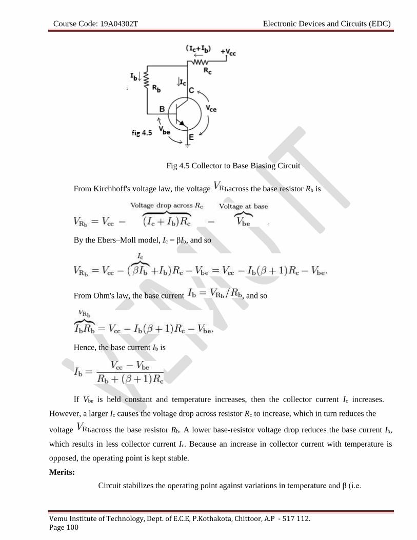
Course Code: 19A04302T Electronic Devices and Circuits (EDC)
Vemu Institute of Technology, Dept. of E.C.E, P.Kothakota, Chittoor, A.P - 517 112. Page 100
Fig 4.5 Collector to Base Biasing Circuit
From Kirchhoff's voltage law, the voltage across the base resistor Rb is
By the Ebers–Moll model, Ic = βIb, and so
From Ohm's law, the base current , and so
Hence, the base current Ib is
If Vbe is held constant and temperature increases, then the collector current Ic increases.
However, a larger Ic causes the voltage drop across resistor Rc to increase, which in turn reduces the
voltage across the base resistor Rb. A lower base-resistor voltage drop reduces the base current Ib,
which results in less collector current Ic. Because an increase in collector current with temperature is
opposed, the operating point is kept stable.
Merits:
Circuit stabilizes the operating point against variations in temperature and β (i.e.
Course Code: 19A04302T Electronic Devices and Circuits (EDC)
Vemu Institute of Technology, Dept. of E.C.E, P.Kothakota, Chittoor, A.P - 517 112. Page 101
replacement of transistor) Demerits:
• In this circuit, to keep Ic independent of β, the following condition must be met:
which is the case when
• As β-value is fixed (and generally unknown) for a given transistor, this relation can be satisfied
either by keeping Rc fairly large or making Rb very low.
• If Rc is large, a high Vcc is necessary, which increases cost as well as precautions necessary while
handling.
• If Rb is low, the reverse bias of the collector–base region is small, which limits the range of
collector voltage swing that leaves the transistor in active mode.
• The resistor Rb causes an AC feedback, reducing the voltage gain of the amplifier. This
undesirable effect is a trade-off for greater Q-point stability.
Usage: The feedback also decreases the input impedance of the amplifier as seen from the base, which
can be advantageous. Due to the gain reduction from feedback, this biasing form is used only when the
trade-off for stability is warranted.

Course Code: 19A04302T Electronic Devices and Circuits (EDC)
Vemu Institute of Technology, Dept. of E.C.E, P.Kothakota, Chittoor, A.P - 517 112. Page 102
3) COLLECTOR –EMITTER FEEDBACK BIAS:
Fig 4.6 Collector-Emitter Biasing Circuit
The above fig4.6 shows the collector –emitter feedback bias circuit that can be obtained by
applying both the collector feedback and emitter feedback. Here the collector feedback is provided by
connecting a resistance RB from the collector to the base and emitter feedback is provided by
connecting an emitter Re from emitter to ground. Both feed backs are used to control collector current
and base current IB in the opposite direction to increase the stability as compared to the previous biasing
circuits.
4) VOLTAGE DIVIDER BIAS OR SELF BIAS OR EMITTER BIAS
Fig 4.7 Voltage Divider Biasing Circuit

Course Code: 19A04302T Electronic Devices and Circuits (EDC)
Vemu Institute of Technology, Dept. of E.C.E, P.Kothakota, Chittoor, A.P - 517 112. Page 103
The voltage divider as shown in the fig 4.7 is formed using external resistors R1 and R2. The
voltage across R2 forward biases the emitter junction. By proper selection of resistors R1 and R2, the
operating point of the transistor can be made independent of β. In this circuit, the voltage divider holds
the base voltage fixed independent of base current provided the divider current is large compared to the
base current. However, even with a fixed base voltage, collector current varies with temperature (for
example) so an emitter resistor is added to stabilize the Q-point, similar to the above circuits with
emitter resistor.
In this circuit the base voltage is given by:
voltage across
provided .
Also
For the given circuit,
Let the current in resistor R1 is I1 and this is divided into two parts – current through base and
resistor R2. Since the base current is very small so for all practical purpose it is assumed that I1 also
flows through R2, so we have
Applying KVL in the circuit, we have

Course Code: 19A04302T Electronic Devices and Circuits
(EDC)
Vemu Institute of Technology, Dept. of E.C.E, P.Kothakota, Chittoor, A.P - 517 112. Page 104
It is apparent from above expression that the collector current is independent of ? thus the
stability is excellent. In all practical cases the value of VBE is quite small in comparison to the V2, so
it can be ignored in the above expression so the collector current is almost independent of the transistor
parameters thus this arrangement provides excellent stability.
Again applying KVL in collector circuit, we have
The resistor RE provides stability to the circuit. If the current through the collector rises, the
voltage across the resistor RE also rises. This will cause VCE to increase as the voltage V2 is
independent of collector current. This decreases the base current, thus collector current increases to its
former value.
Stability factor for such circuit arrangement is given by
If Req/RE is very small compared to 1, it can be ignored in the above expression thus we have

Course Code: 19A04302T Electronic Devices and Circuits
(EDC)
Vemu Institute of Technology, Dept. of E.C.E, P.Kothakota, Chittoor, A.P - 517 112. Page 105
Which is excellent since it is the smallest possible value for the stability. In actual practice the
value of stability factor is around 8-10, since Req/RE cannot be ignored as compared to 1.
Merits:
• Unlike above circuits, only one dc supply is necessary.
• Operating point is almost independent of β variation.
• Operating point stabilized against shift in temperature.
Demerits:
• In this circuit, to keep IC independent of β the following condition must be met:
which is approximately the case if
• where R1 || R2 denotes the equivalent resistance of R1 and R2 connected in parallel.
• As β-value is fixed for a given transistor, this relation can be satisfied either by keeping RE
fairly large, or making R1||R2 very low.
• If RE is of large value, high VCC is necessary. This increases cost as well as precautions
necessary while handling.
• If R1 || R2 is low, either R1 is low, or R2 is low, or both are low. A low R1 raises VB closer to
VC, reducing the available swing in collector voltage, and limiting how large RC can be made
without driving the transistor out of active mode. A low R2 lowers Vbe, reducing the allowed
collector current. Lowering both resistor values draws more current from the power supply and
lowers the input resistance of the amplifier as seen from the base.
• AC as well as DC feedback is caused by RE, which reduces the AC voltage gain of the
amplifier. A method to avoid AC feedback while retaining DC feedback is discussed below.
Usage: The circuit's stability and merits as above make it widely used for linear circuits.
4.6 BIAS COMPENSATION USING DIODE AND TRANSISTOR
The various biasing circuits considered use some type of negative feedback to stabilize the
operation point. Also, diodes, thermistors and sensistors can be used to compensate for variations in
current.

Course Code: 19A04302T Electronic Devices and Circuits
(EDC)
Vemu Institute of Technology, Dept. of E.C.E, P.Kothakota, Chittoor, A.P - 517 112. Page 106
DIODE COMPENSATION:
The following fig4.8 shows a transistor amplifier with a diode D connected across the base-
emitter junction for compensation of change in collector saturation current ICO. The diode is of the
same material as the transistor and it is reverse biased by e the emitter-base junction voltage VBE,
allowing the diode reverse saturation current IO to flow through diode D. The base current IB=I-IO.
As long as temperature is constant, diode D operates as a resistor. As the temperature increases,
ICO of the transistor increases. Hence, to compensate for this, the base current IB should be decreased.
The increase in temperature will also cause the leakage current IO through D to increase and
thereby decrease the base current IB. This is the required action to keep Ic constant.
This type of bias compensation does not need a change in Ic to effect the change in IC, as both
IO and ICO can track almost equally according to the change in temperature.
THERMISTOR COMPENSATION:
Fig 4.9 Thermistor Compensation

Course Code: 19A04302T Electronic Devices and Circuits
(EDC)
Vemu Institute of Technology, Dept. of E.C.E, P.Kothakota, Chittoor, A.P - 517 112. Page 107
The following fig4.9 a thermistor RT, having a negative temperature coefficient is connected in
parallel with R2. The resistance of thermistor decreases exponentially with increase of temperature. An
increase of temperature will decrease the base voltage VBE, reducing IB and IC.
SENSISTOR COMPENSATION:
In the following fig4.10 shown a sensistor Rs having a positive temperature coefficient is
connected across R1 or RE. Rs increases with temperature. As the temperature increases, the equivalent
resistance of the parallel combination of R1 and Rs also increases and hence VBE decreases, reducing
IB and Ic. This reduced Ic compensates for increased Ic caused by the increase in VBE, ICO and β due to
temperature.
Fig 4.10 Sensistor Compensation
4.7 THERMAL RUNAWAY AND THERMAL STABILITY
THERMAL RUNAWAY:
The collector current for the CE circuit is given by The three
variables in the equation, β, , and increases with rise in temperature. In particular, the reverse
saturation current or leakage current changes greatly with temperature. Specifically it doubles for

Course Code: 19A04302T Electronic Devices and Circuits
(EDC)
Vemu Institute of Technology, Dept. of E.C.E, P.Kothakota, Chittoor, A.P - 517 112. Page 108
every 10oC rise in temperature. The collector current causes the collector base junction temperature
to rise
which in turn, increase , as a result will increase still further, which will further rise the
temperature at the collector base junction. This process will become cumulative leading at the collector
base junction. This process will become cumulative leading to “thermal runaway”. Consequently, the
ratings of the transistor are exceeded which may destroy the transistor itself.
The collector is made larger in size than the emitter in order to help the heat developed at the
collector junction. However if the circuit is designed such that the base current is made to decrease
automatically with rise in temperature, then the decrease in will compensate for increase in the
, keeping almost constant.
THERMAL RESISTANCE
Consider transistor used in a circuit where the ambient temperature of the air around the
transistor is TAoC and the temperature of the collector-base junction of the transistor is TJ
oC.
Due to heating within the transistor TJ is higher than TA. As the temperature difference TJ- TA is
greater, the power dissipated in the transistor, PD will be greater, i.e, TJ- TA PD
The equation can be written as TJ- TA PD. , where is the constant of proportionality and
is called the Thermal resistance. Rearranging the above equation = TJ- TA /PD. Hence is measured
in oC/W which may be as small as 0.2 oC/W for a high power transistor that has an efficient heat sink
or up to 1000oC/W for small signal, low power transistor which have no cooling provision.
As Θ represents total thermal resistance from a transistor junction to the ambient temperature, it
is referred to as ΘJ-A. However, for power transistors, thermal resistance is given form junction to case,
ΘJ-C.
The amount resistance from junction to ambience is considered to consist of 2 parts.
ΘJ-A = ΘJ-C - ΘC-A.
Which indicates the heat dissipated in the junction must make its way to the surrounding air
through two series paths from junction to case and from case to air. Hence the power dissipated.
Course Code: 19A04302T Electronic Devices and Circuits
(EDC)
Vemu Institute of Technology, Dept. of E.C.E, P.Kothakota, Chittoor, A.P - 517 112. Page 109
PD = (TJ- TA Θ J-A
=(TJ- TA Θ J-C + Θ C-A)
ΘJ-C is determined by the type of manufacture of the transistor and how it is located I the case, but ΘC-A
is determined by the surface area of the case or flange and its contact with air. If the effective surface
area of the transistor case could be increased, the resistance to heat flows, or could be increased ΘC-A,
could be decreased. This can be achieved by the use of a heat sink.
The heat sink is a relatively large, finned, usually black metallic heat conducting device in close
contact with transistor case or flange. Many versions of heat sink exist depending upon the shape and
size of the transistor. Larger the heat sink smaller is the thermal resistance ΘHS-A.
This thermal resistance is not added to ΘC-A in series, but is instead in parallel with it and if ΘHS-A is
much less than ΘC-A, then ΘC-A will be reduced significantly, thereby improving the dissipation
capability of the transistor. Thus
Θ J-A =Θ J-C + Θ C-A|| ΘHS-A. 4.8 CONDITION FOR THERMAL STABILITY
For preventing thermal runaway, the required condition I the rate at which the heat is released
at the collector junction should not exceed the rate at which the heat can be dissipated under steady
state condition. Hence the condition to be satisfied to avoid thermal runaway is given by

Course Code: 19A04302T Electronic Devices and Circuits
(EDC)
Vemu Institute of Technology, Dept. of E.C.E, P.Kothakota, Chittoor, A.P - 517 112. Page 110
UNIT-5 A) Small Signal Low Frequency Transistor Amplifier Models
Small signal low frequency transistor Models:
All the transistor amplifiers are two port networks having two voltages and two currents.
The positive directions of voltages and currents are shown in fig. 1.
Fig. 1
A two-port network is represented by four external variables: voltage V1 and current I1 at the
input port, and voltage V2 and current I2 at the output port, so that the two-port network can be treated
as a black box modeled by the relationships between the four variables,V1,V2, I1,I2 . Out of four
variables two can be selected as are independent variables and two are dependent variables.The
dependent variables can be expressed interns of independent variables. This leads to various two port
parameters out of which the following three are important:
1. Impedance parameters (z-parameters)
2. Admittance parameters (y-parameters)
3. Hybrid parameters (h-parameters)
Z-parameters:
A two-port network can be described by z-parameters as In matrix form, the above equation can be rewritten as
Where
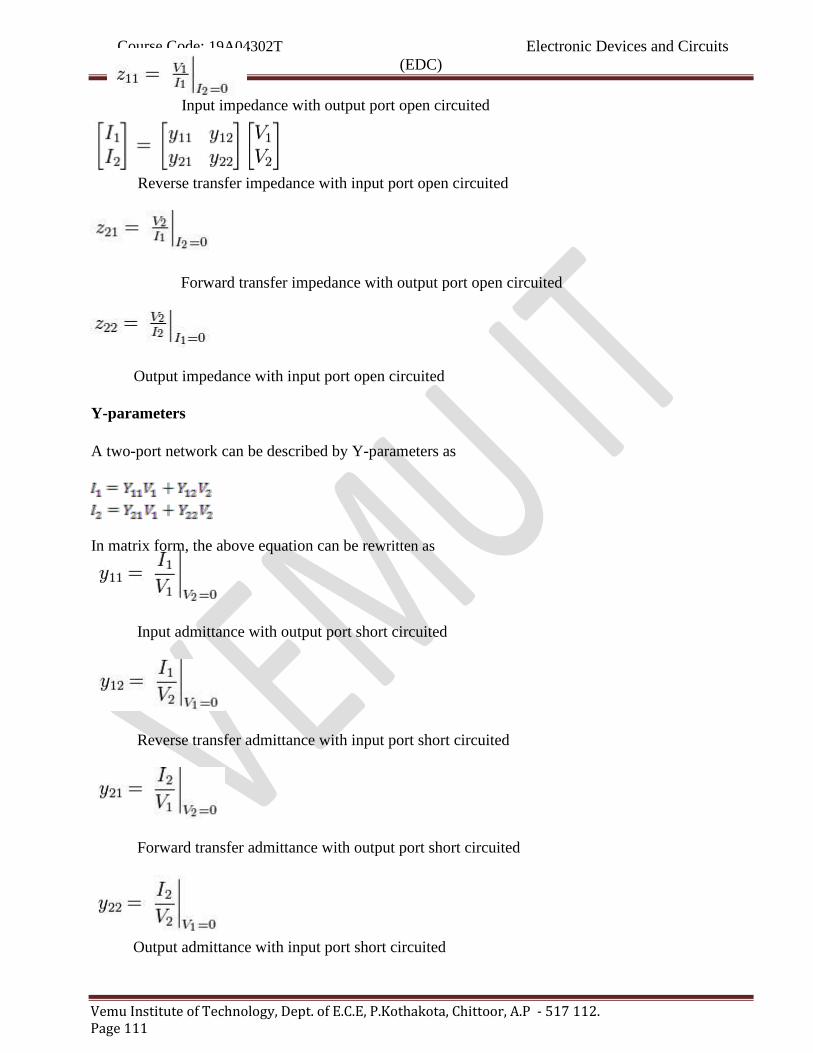
Course Code: 19A04302T Electronic Devices and Circuits
(EDC)
Vemu Institute of Technology, Dept. of E.C.E, P.Kothakota, Chittoor, A.P - 517 112. Page 111
Input impedance with output port open circuited
Reverse transfer impedance with input port open circuited
Forward transfer impedance with output port open circuited
Output impedance with input port open circuited
Y-parameters
A two-port network can be described by Y-parameters as
In matrix form, the above equation can be rewritten as
Input admittance with output port short circuited
Reverse transfer admittance with input port short circuited
Forward transfer admittance with output port short circuited
Output admittance with input port short circuited
Course Code: 19A04302T Electronic Devices and Circuits
(EDC)
Vemu Institute of Technology, Dept. of E.C.E, P.Kothakota, Chittoor, A.P - 517 112. Page 112
Hybrid parameters (h-parameters)
If the input current I1 and output voltage V2 are taken as independent variables, the dependent
variables V1 and I2 can be written as
Where h11, h12, h21, h22 are called as hybrid parameters.
Input impedance with o/p port short circuited
Reverse voltage transfer ratio with i/p port open circuited
Forward voltage transfer ratio with o/p port short circuited
Output impedance with i/p port open circuited
THE HYBRID MODEL FOR TWO PORT NETWORK:
Based on the definition of hybrid parameters the mathematical model for two pert networks
known as h-parameter model can be developed.
The hybrid equations can be written as:
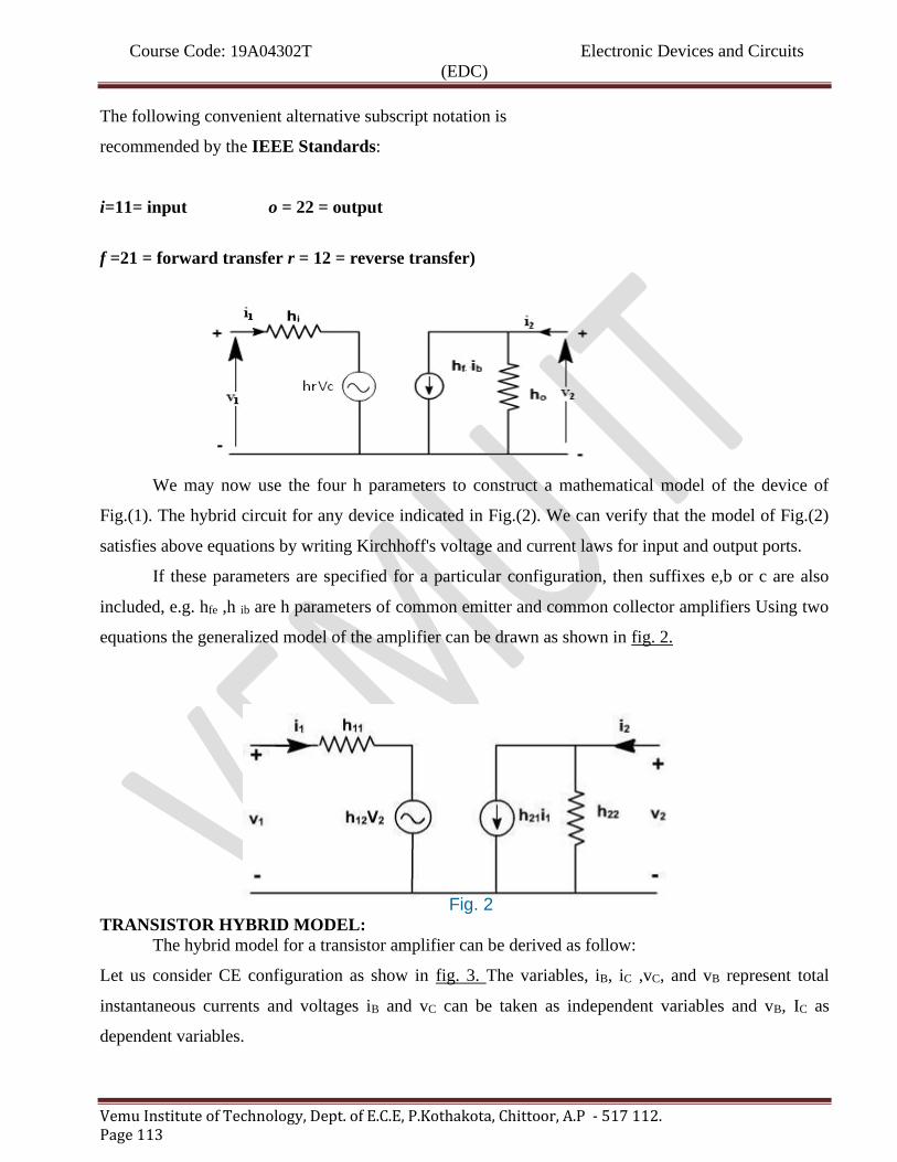
Course Code: 19A04302T Electronic Devices and Circuits
(EDC)
Vemu Institute of Technology, Dept. of E.C.E, P.Kothakota, Chittoor, A.P - 517 112. Page 113
The following convenient alternative subscript notation is
recommended by the IEEE Standards:
i=11= input o = 22 = output
f =21 = forward transfer r = 12 = reverse transfer)
We may now use the four h parameters to construct a mathematical model of the device of
Fig.(1). The hybrid circuit for any device indicated in Fig.(2). We can verify that the model of Fig.(2)
satisfies above equations by writing Kirchhoff's voltage and current laws for input and output ports.
If these parameters are specified for a particular configuration, then suffixes e,b or c are also
included, e.g. hfe ,h ib are h parameters of common emitter and common collector amplifiers Using two
equations the generalized model of the amplifier can be drawn as shown in fig. 2.
Fig. 2 TRANSISTOR HYBRID MODEL:
The hybrid model for a transistor amplifier can be derived as follow:
Let us consider CE configuration as show in fig. 3. The variables, iB, iC ,vC, and vB represent total
instantaneous currents and voltages iB and vC can be taken as independent variables and vB, IC as
dependent variables.

Course Code: 19A04302T Electronic Devices and Circuits
(EDC)
Vemu Institute of Technology, Dept. of E.C.E, P.Kothakota, Chittoor, A.P - 517 112. Page 114
Fig. 3 VB = f1 (iB ,vC ) IC = f2 (iB ,vC).
Using Taylor 's series expression, and neglecting higher order terms we obtain.
The partial derivatives are taken keeping the collector voltage or base current constant. The vB, vC, iB,
iC represent the small signal (incremental) base and collector current and voltage and can be
represented as vB, iC, iB ,vC
The model for CE configuration is shown in fig. 4.

Course Code: 19A04302T Electronic Devices and Circuits (EDC)
Vemu Institute of Technology, Dept. of E.C.E, P.Kothakota, Chittoor, A.P - 517 112. Page 115
Fig. 4
To determine the four h-parameters of transistor amplifier, input and output characteristic are
used. Input characteristic depicts the relationship between input voltage and input current with output
voltage as parameter. The output characteristic depicts the relationship between output voltage and
output current with input current as parameter. Fig. 5, shows the output characteristics of CE amplifier.
Fig. 5
The current increments are taken around the quiescent point Q which corresponds to iB = IB and to the
collector voltage VCE = VC
The value of hoe at the quiescent operating point is given by the slope of the output characteristic at
the operating point (i.e. slope of tangent AB).

Course Code: 19A04302T Electronic Devices and Circuits (EDC)
Vemu Institute of Technology, Dept. of E.C.E, P.Kothakota, Chittoor, A.P - 517 112. Page 116
hie is the slope of the appropriate input on fig. 6, at the operating point (slope of tangent EF at Q).
Fig. 6 A vertical line on the input characteristic represents constant base current. The parameter hre can be
obtained from the ratio (VB2– V B1 ) and (VC2– V C1 ) for at Q.
Typical CE h-parameters of transistor 2N1573 are given below:
hie = 1000 ohm.
hre = 2.5 * 10 –4
hfe = 50
hoe = 25 A / V
ANALYSIS OF A TRANSISTOR AMPLIFIER USING H-PARAMETERS:
To form a transistor amplifier it is only necessary to connect an external load and signal source as
indicated in fig. 1 and to bias the transistor properly.
Fig. 1

Course Code: 19A04302T Electronic Devices and Circuits (EDC)
Vemu Institute of Technology, Dept. of E.C.E, P.Kothakota, Chittoor, A.P - 517 112. Page 117
Consider the two-port network of CE amplifier. RS is the source resistance and ZL is the load
impedence h-parameters are assumed to be constant over the operating range. The ac equivalent circuit
is shown in fig. 2. (Phasor notations are used assuming sinusoidal voltage input). The quantities of
interest are the current gain, input impedence, voltage gain, and output impedence.
Current gain:
For the transistor amplifier stage, Ai is defined as the ratio of output to input currents.
Input impedance:
The impedance looking into the amplifier input terminals ( 1,1' ) is the input impedance Zi

Course Code: 19A04302T Electronic Devices and Circuits
(EDC)
Vemu Institute of Technology, Dept. of E.C.E, P.Kothakota, Chittoor, A.P - 517 112. Page 118
Voltage gain:
The ratio of output voltage to input voltage gives the gain of the transistors.
Output Admittance:
It is defined as
Av is the voltage gain for an ideal voltage source (Rv = 0).
Consider input source to be a current source IS in parallel with a resistance RS as shown in fig. 3.
Fig. 3
In this case, overall current gain AIS is defined as

Course Code: 19A04302T Electronic Devices and Circuits (EDC)
Vemu Institute of Technology, Dept. of E.C.E, P.Kothakota, Chittoor, A.P - 517 112. Page 119
h-parameters
To analyze multistage amplifier the h-parameters of the transistor used are obtained from
manufacture data sheet. The manufacture data sheet usually provides h-parameter in CE configuration.
These parameters may be converted into CC and CB values. For example fig. 4 hrc in terms of CE
parameter can be obtained as follows.
Fig. 4
For CE transistor configuration
Vbe = hie Ib + hre Vce
Ic = h fe Ib + hoe Vce
The circuit can be redrawn like CC transistor configuration as shown in fig. 5.
Vbc = hie Ib + hrc Vec
Ic = hfe Ib + hoe Vec hybrid model for transistor in three different configurations

Course Code: 19A04302T Electronic Devices and Circuits (EDC)
Vemu Institute of Technology, Dept. of E.C.E, P.Kothakota, Chittoor, A.P - 517 112. Page 120
Typical h-parameter values for a transistor
Parameter CE CC CB
hi 1100 Ω 1100 Ω 22 Ω
hr 2.5 × 10⁻⁴ 1 3 × 10⁻⁴
hf 50 -51 -0.98
ho 25 µA/V 25 µA/V 0.49 µA/V
Analysis of a Transistor amplifier circuit using h-parameters
A transistor amplifier can be constructed by connecting an external load and signal source and
biasing the transistor properly.

COURSE MATERIAL
Fig.1.4 Basic Amplifier Circuit
The two port network of Fig. 1.4 represents a transistor in any one of its configuration. It is
assumed that h-parameters remain constant over the operating range. The input is sinusoidal and I1,V-
1,I2 and V2 are phase quantities
Fig. 1.5 Transistor replaced by its Hybrid Model
Current Gain or Current Amplification (Ai)
For transistor amplifier the current gain Ai is defined as the ratio of output current to input
current,i.e,
Ai =IL /I1 = -I2 / I1 From the circuit of Fig
I2= hf I1 + hoV2
Substituting V2 = ILZL = -I2ZL
I2= hf I1- I2ZL ho
I2 + I2ZL ho = hf I1
I2( 1+ ZL ho) = hf I1
Ai = -I2 / I1 = - hf / ( 1+ ZL ho)

COURSE MATERIAL
Therefore,
Ai = - hf / ( 1+ ZL ho) Input Impedance (Zi)
In the circuit of Fig , RS is the signal source resistance .The impedance seen when looking into the
amplifier terminals (1,1’) is the amplifier input impedance Zi,
Zi = V1 / I1
From the input circuit of Fig V1 = hi I1 + hrV2
Zi = ( hi I1 + hrV2) / I1
= hi + hr V2 / I1
Substituting
V2 = -I2 ZL = A1I1ZL
Zi = hi + hr A1I1ZL / I1
= hi + hr A1ZL
Substituting for Ai
Zi = hi - hf hr ZL / (1+ hoZL)
= hi - hf hr ZL / ZL(1/ZL+ ho) Taking the Load admittance as YL =1/ ZL
Zi = hi - hf hr / (YL + ho)
Voltage Gain or Voltage Gain Amplification Factor(Av)
The ratio of output voltage V2 to input voltage V1 give the voltage gain of the transistor i.e,
Av = V2 / V1
Substituting
V2 = -I2 ZL = A1I1ZL
Av = A1I1ZL / V1 = AiZL / Zi
Output Admittance (Yo)
Yo is obtained by setting VS to zero, ZL to infinity and by driving the output terminals from a generator

COURSE MATERIAL
V2. If the current V2 is I2 then Yo= I2/V2 with VS=0 and RL= ∞.
From the circuit of fig
I2= hf I1 + hoV2
Dividing by V2,
I2 / V2 = hf I1/V2 + ho
With V2= 0, by KVL in input circuit,
RSI1 + hi I1 + hrV2 = 0
(RS + hi) I1 + hrV2 = 0
Hence, I2 / V2 = -hr / (RS + hi)
= hf (-hr/( RS + hi)+ho
Yo= ho- hf hr/( RS + hi)
The output admittance is a function of source resistance. If the source impedence is resistive then Yo is
real.
Voltage Amplification Factor(Avs) taking into account the resistance (Rs) of the source
Fig. 5.6 Thevenin’s Equivalent Input Circuit
This overall voltage gain Avs is given by
Avs = V2 / VS = V2V1 / V1VS = Av V1/ VS
From the equivalent input circuit using Thevenin’s equivalent for the source shown in Fig. 5.6 V1 =
VS Zi / (Zi + RS)
V1 / VS = Zi / ( Zi + RS)
Then,

COURSE MATERIAL
Avs = Av Zi / ( Zi + RS)
Substituting
Av = AiZL / Zi
Avs = AiZL / ( Zi + RS)
Avs = AiZL RS / ( Zi + RS) RS
Avs = AisZL / RS
Current Amplification (Ais) taking into account the sourse Resistance(RS)
Fig. 1.7 Norton’s Equivalent Input Circuit
The modified input circuit using Norton’s equivalent circuit for the calculation of Ais is shown in Fig.
1.7 Overall Current Gain, Ais = -I2 / IS = - I2I1 /I1 IS = Ai I1/IS
Operating Power Gain (AP)
The operating power gain AP of the transistor is defined as
AP = P2 / P1 = -V2 I2 / V1 I1 = AvAi = Ai AiZL/ Zi
AP = Ai2(ZL/ Zi)
Small Signal analysis of a transistor amplifier
Ai = - hf / ( 1+ ZL ho) Av = AiZL / Zi
Zi = hi + hr A1ZL = hi - hf hr / (YL + ho) Avs = Av Zi / ( Zi + RS) = AiZL / ( Zi + RS)
= AisZL / RS
Yo= ho- hf hr/( RS + hi) = 1/ Zo Ais = Ai RS / (RS + Zi) = Avs = Ais RS/ ZL

COURSE MATERIAL
B) FET AMPLIFIERS 5.10 INTRODUCTION
Field Effect Transistor (FET) amplifiers provide an excellent voltage gain and high input
impedence. Because of high input impedence and other characteristics of JFETs they are preferred over
BJTs for certain types of applications.
There are 3 basic FET circuit configurations: i)Common Source ii)Common Drain iii)Common Gain
Similar to BJT CE,CC and CB circuits, only difference is in BJT large output collector current
is controlled by small input base current whereas FET controls output current by means of small input voltage. In both the cases output current is controlled variable.
FET amplifier circuits use voltage controlled nature of the JFET. In Pinch off region, ID
depends only on VGS.
5.11 Common Source (CS) Amplifier
Fig. 5.1 (a) CS Amplifier (b) Small-signal equivalent circuit
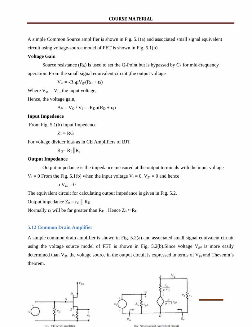
COURSE MATERIAL
A simple Common Source amplifier is shown in Fig. 5.1(a) and associated small signal equivalent
circuit using voltage-source model of FET is shown in Fig. 5.1(b)
Voltage Gain
Source resistance (RS) is used to set the Q-Point but is bypassed by CS for mid-frequency
operation. From the small signal equivalent circuit ,the output voltage
VO = -RDµVgs(RD + rd)
Where Vgs = Vi , the input voltage,
Hence, the voltage gain,
AV = VO / Vi = -RDµ(RD + rd)
Input Impedence
From Fig. 5.1(b) Input Impedence
Zi = RG
For voltage divider bias as in CE Amplifiers of BJT
RG= R1R2
Output Impedance
Output impedance is the impedance measured at the output terminals with the input voltage
VI = 0 From the Fig. 5.1(b) when the input voltage Vi = 0, Vgs = 0 and hence
µ Vgs = 0
The equivalent circuit for calculating output impedance is given in Fig. 5.2.
Output impedance Zo = rd RD
Normally rd will be far greater than RD . Hence Zo ≈ RD
5.12 Common Drain Amplifier A simple common drain amplifier is shown in Fig. 5.2(a) and associated small signal equivalent circuit
using the voltage source model of FET is shown in Fig. 5.2(b).Since voltage Vgd is more easily
determined than Vgs, the voltage source in the output circuit is expressed in terms of Vgs and Thevenin’s
theorem.
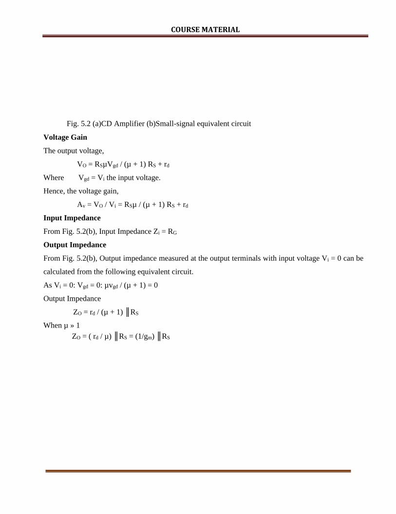
COURSE MATERIAL
Fig. 5.2 (a)CD Amplifier (b)Small-signal equivalent circuit Voltage Gain
The output voltage,
VO = RSµVgd / (µ + 1) RS + rd
Where Vgd = Vi the input voltage.
Hence, the voltage gain,
Av = VO / Vi = RSµ / (µ + 1) RS + rd
Input Impedance
From Fig. 5.2(b), Input Impedance Zi = RG
Output Impedance
From Fig. 5.2(b), Output impedance measured at the output terminals with input voltage Vi = 0 can be
calculated from the following equivalent circuit.
As Vi = 0: Vgd = 0: µvgd / (µ + 1) = 0
Output Impedance
ZO = rd / (µ + 1) RS When µ » 1
ZO = ( rd / µ) RS = (1/gm) RS


![[Kishore] Electronic Devices and Circuits](https://img.dokumen.tips/doc/110x75/55cf94c4550346f57ba43b2a/kishore-electronic-devices-and-circuits.jpg)