Embed Size (px)
Citation preview

8/9/2019 r07a1ec06 Electronic Devices and Circuits
http://slidepdf.com/reader/full/r07a1ec06-electronic-devices-and-circuits 1/8
Seminar Topics - Scholarships - Admission/Entrance Exam Notifications
USA-UK-Australia-Germany-France-NewZealand Universities List
Engineering-MBA-MCA-Medical-Pharmacy-B.Ed-Law Colleges Information
www.andhracolleges.com The Complete Information About Colleges in Andhra Pradesh
Code No: Z0421 / R07 Set No. 1
I B.Tech - Regular Examinations, June 2009ELECTRONIC DEVICES AND CIRCUITS
( Common to Electronics & Communication Engineering, Computer Science& Engineering, Electronics & Instrumentation Engineering, Bio-Medical
Engineering, Information Technology, Electronics & Control Engineering,Computer Science & Systems Engineering, Electronics & Telematics,Electronics & Computer Engineering and Instrumentation & Control
Engineering)Time: 3 hours Max Marks: 80
Answer any FIVE QuestionsAll Questions carry equal marks
⋆ ⋆ ⋆ ⋆ ⋆
1. What are the main parts of the CRT? Explain briefly with neat sketch. [16]
2. (a) Short notes on LED voltage drop and current.
(b) Write short notes on Multi colour LED. [10+6]
3. (a) Draw the circuit diagram of HWR. Explain its working. What is the frequencyof ripple in its output
(b) A HWR circuit supplies 100mA d.c to a 250 Ω load. Find the d.c outputvoltage, PIV rating of a diode and the r.m.s. voltage for the transformersupplying the rectifier. [8+8]
4. Derive an Eber’s Moll equation for a transistor. [16]
5. (a) Explain the criteria for fixing operating point.
(b) List out the different types of biasing methods. [12+4]
6. A transistor used in a CC Circuit as shown in Figure 6. has the following set of hparameters.hic = 2 KΩ, hfc = -51, hrc = 1, hoc = 25 × 10−6
Find the values of input and output resistances, current and voltage gains of theamplifier stage. Use the approximate analysis. [16]
1 of 2
8/9/2019 r07a1ec06 Electronic Devices and Circuits
http://slidepdf.com/reader/full/r07a1ec06-electronic-devices-and-circuits 2/8
Seminar Topics - Scholarships - Admission/Entrance Exam Notifications
USA-UK-Australia-Germany-France-NewZealand Universities List
Engineering-MBA-MCA-Medical-Pharmacy-B.Ed-Law Colleges Information
www.andhracolleges.com The Complete Information About Colleges in Andhra Pradesh
Code No: Z0421 / R07 Set No. 1
Figure 6
7. Enumerate the effects of negative feedback on the various characteristics of theamplifier. [16]
8. (a) Define:i. Damped Oscillation
ii. Un Damped oscillation.
(b) Why an LC tank circuit, once excited, does not produce sustained oscillation?Explain it briefly?
(c) Give the two Bark Hansen condition required for sinusoidal oscillations to besustained.
(d) What are the factors which affect the frequency stability of an oscillator?[4+6+2+4]
⋆ ⋆ ⋆ ⋆ ⋆
2 of 2

8/9/2019 r07a1ec06 Electronic Devices and Circuits
http://slidepdf.com/reader/full/r07a1ec06-electronic-devices-and-circuits 3/8
Seminar Topics - Scholarships - Admission/Entrance Exam Notifications
USA-UK-Australia-Germany-France-NewZealand Universities List
Engineering-MBA-MCA-Medical-Pharmacy-B.Ed-Law Colleges Information
www.andhracolleges.com The Complete Information About Colleges in Andhra Pradesh
Code No: Z0421 / R07 Set No. 2
I B.Tech - Regular Examinations, June 2009ELECTRONIC DEVICES AND CIRCUITS
( Common to Electronics & Communication Engineering, Computer Science& Engineering, Electronics & Instrumentation Engineering, Bio-Medical
Engineering, Information Technology, Electronics & Control Engineering,Computer Science & Systems Engineering, Electronics & Telematics,Electronics & Computer Engineering and Instrumentation & Control
Engineering)Time: 3 hours Max Marks: 80
Answer any FIVE QuestionsAll Questions carry equal marks
⋆ ⋆ ⋆ ⋆ ⋆
1. In a parallel place diode, the cathode and anode are spaced 5mm apart and theanode is kept at 200V d.c. with respect to cathode. Calculate the velocity and thedistance travelled by an electron after a time of 0.5ns, when [16]
(a) The initial velocity of an electron is zero and
(b) The initial velocity is 2×10⁶ m/s in the direction towards the anode.
2. Explain in detail PN junction energy band diagram of a PN diode. [16]
3. A voltage of 200 cos wt is applied to HWR with load resistance of 5 KΩ. find themaximum d.c current component, r.m.s. current, ripple ractor, TUF and rectifierefficiency. [16]
4. Explain the input and output characteristics of common base transistor configura-tion. [16]
5. Briefly explain fixed bias with Emitter Feed back. Also find the stability of thisbias. [16]
6. (a) Draw the low frequency hybrid equivalent. Circuit for CE & CB amplifier.
(b) Give the approximate h-parameter conversion formulae for CB and CC con-figuration in terms of CE.
(c) Give the advantages of h-parameter analysis.
(d) Give the procedure to form the approximate h - model from exact h - modelof amplifier. [4+6+3+3]
7. A negative feedback of 0.0005 is applied to an amplifier whose open loop gain is60dB. If the open loop gain gets reduced by 132%, how much the overall gain getsaltered? [16]
8. (a) A colpitts oscillator is designed with C 1 = 100 PF and C 2 = 7500 PF. Theinductance is variable. Find the range of inductance value, if the frequency of oscillation is to vary between 950 KHz and 2050 KHz.
1 of 2

8/9/2019 r07a1ec06 Electronic Devices and Circuits
http://slidepdf.com/reader/full/r07a1ec06-electronic-devices-and-circuits 4/8
Seminar Topics - Scholarships - Admission/Entrance Exam Notifications
USA-UK-Australia-Germany-France-NewZealand Universities List
Engineering-MBA-MCA-Medical-Pharmacy-B.Ed-Law Colleges Information
www.andhracolleges.com The Complete Information About Colleges in Andhra Pradesh
Code No: Z0421 / R07 Set No. 2
(b) A Hartely oscillator is designed with L2 = 20µH and a variable capacitance.Find the range of capacitance values. If the frequency of oscillation is variedbetween 950 KHz to 2050 KHz. [10+6]
⋆ ⋆ ⋆ ⋆ ⋆
2 of 2
8/9/2019 r07a1ec06 Electronic Devices and Circuits
http://slidepdf.com/reader/full/r07a1ec06-electronic-devices-and-circuits 5/8
Seminar Topics - Scholarships - Admission/Entrance Exam Notifications
USA-UK-Australia-Germany-France-NewZealand Universities List
Engineering-MBA-MCA-Medical-Pharmacy-B.Ed-Law Colleges Information
www.andhracolleges.com The Complete Information About Colleges in Andhra Pradesh
Code No: Z0421 / R07 Set No. 3
I B.Tech - Regular Examinations, June 2009ELECTRONIC DEVICES AND CIRCUITS
( Common to Electronics & Communication Engineering, Computer Science& Engineering, Electronics & Instrumentation Engineering, Bio-Medical
Engineering, Information Technology, Electronics & Control Engineering,Computer Science & Systems Engineering, Electronics & Telematics,Electronics & Computer Engineering and Instrumentation & Control
Engineering)Time: 3 hours Max Marks: 80
Answer any FIVE QuestionsAll Questions carry equal marks
⋆ ⋆ ⋆ ⋆ ⋆
1. Two plane parallel plates A and B are placed 3 mm apart and potential of b ismade 200 V positive with respect to plate A. An electron starts from rest fromplate A. Calculate
(a) The velocity of the electron on reaching plate B.
(b) Time taken by the electron to travel from plate A to plate B, and
(c) Kinetic energy of the electron on reaching the plate B. [16]
2. (a) Explain about semiconductor, Insulator & Conductor with neat sketch.
(b) State the Einstein relationship for semiconductor.
(c) State paulis exclusion principle. [6+5+5]
3. Derive the ripple factor of capacitor filter. [16]
4. Derive the analytical expression for transistgor characteristics. [16]
5. In a germanium transistor CE amplifier biased by feedback resistor method , V CC = 20 V, V BE = 0.2 V, β = 100 and the operating point is chosen such that V CE =10.4 V and I C = 9.9mA, determine the value of RB and RC . [16]
6. A transistor used in a CC Circuit as shown in Figure 6. has the following set of hparameters.hic = 2 KΩ, hfc = -51, hrc = 1, hoc = 25 × 10−6
Find the values of input and output resistances, current and voltage gains of theamplifier stage. Use the approximate analysis. [16]
1 of 2

8/9/2019 r07a1ec06 Electronic Devices and Circuits
http://slidepdf.com/reader/full/r07a1ec06-electronic-devices-and-circuits 6/8
Seminar Topics - Scholarships - Admission/Entrance Exam Notifications
USA-UK-Australia-Germany-France-NewZealand Universities List
Engineering-MBA-MCA-Medical-Pharmacy-B.Ed-Law Colleges Information
www.andhracolleges.com The Complete Information About Colleges in Andhra Pradesh
Code No: Z0421 / R07 Set No. 3
Figure 6
7. (a) How the distortion is decreased in negative feedback?
(b) An amplifier has an open loop gain of 1000 and a feedback ration of 0.04. if the open loop gain changes by 10% due to temperature, find the percentagechange in gain of he amplifier with feed back. [10+6]
8. The frequency of oscillation of a colpitts oscillator is given by,f 0= 1
2Π
r
L
C1 C2C1 +C2
This circuit operates at 450 KHz with C 1 = C 2 what will be the oscillation frequencyif the value of C 2 is doubled? [16]
⋆ ⋆ ⋆ ⋆ ⋆
2 of 2

8/9/2019 r07a1ec06 Electronic Devices and Circuits
http://slidepdf.com/reader/full/r07a1ec06-electronic-devices-and-circuits 7/8
Seminar Topics - Scholarships - Admission/Entrance Exam Notifications
USA-UK-Australia-Germany-France-NewZealand Universities List
Engineering-MBA-MCA-Medical-Pharmacy-B.Ed-Law Colleges Information
www.andhracolleges.com The Complete Information About Colleges in Andhra Pradesh
Code No: Z0421 / R07 Set No. 4
I B.Tech - Regular Examinations, June 2009ELECTRONIC DEVICES AND CIRCUITS
( Common to Electronics & Communication Engineering, Computer Science& Engineering, Electronics & Instrumentation Engineering, Bio-Medical
Engineering, Information Technology, Electronics & Control Engineering,Computer Science & Systems Engineering, Electronics & Telematics,Electronics & Computer Engineering and Instrumentation & Control
Engineering)Time: 3 hours Max Marks: 80
Answer any FIVE QuestionsAll Questions carry equal marks
⋆ ⋆ ⋆ ⋆ ⋆
1. An infinitely large parallel plane plates are spaced 0.8 cm apart. The voltage onone of the plates is raised from 0 to 5 V in 1 ns at a uniform rate with respect to theother. After this duration, the potential difference between the plates is suddenlydropped to 0 V and remains the same thereafter. Find
(a) The position of the electron, which started with zero initial velocity from thenegative plate, when the potential difference drops to zero volt,
(b) The total time of transit of the electron from the cathode to the anode. [16]
2. Explain in detail PN junction energy band diagram of a PN diode. [16]
3. (a) Describe transistor shunt regulator.
(b) Calculate the output voltage and zener current in the regulator circuit shownin Figure 3b. [6+10]
Figure 3b
4. (a) Write the reason why the Ico value is negative for NPN transistor & Ico valueis positive for NPN transistor.
(b) Define base spreading reisitance. [10+6]
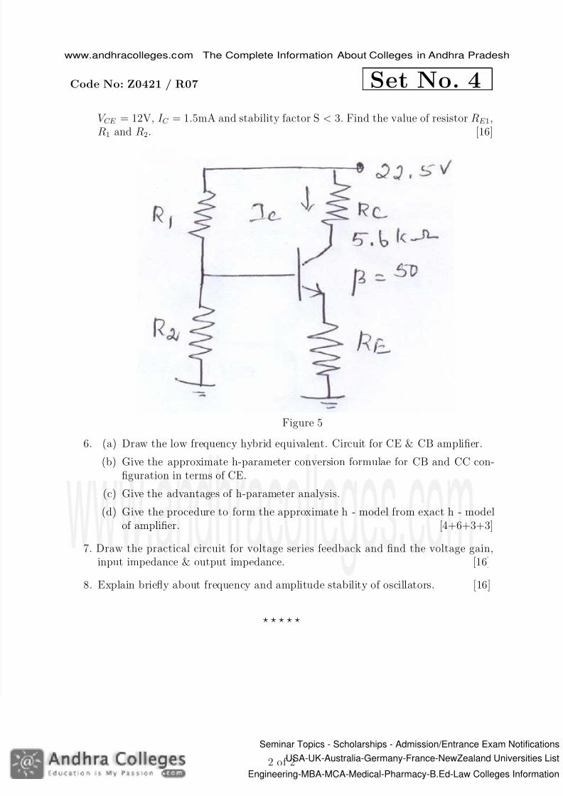
5. A transistor with β = 50; V BE =0.7V, V CC =22.5V, and RC = 5.6KΩ is used inbiasing circuit shown in figure 5. It is designed to establish the quiescent point at
1 of 2
8/9/2019 r07a1ec06 Electronic Devices and Circuits
http://slidepdf.com/reader/full/r07a1ec06-electronic-devices-and-circuits 8/8
Seminar Topics - Scholarships - Admission/Entrance Exam Notifications
USA-UK-Australia-Germany-France-NewZealand Universities List
Engineering MBA MCA Medical Pharmacy B Ed Law Colleges Information
www.andhracolleges.com The Complete Information About Colleges in Andhra Pradesh
Code No: Z0421 / R07 Set No. 4
V CE = 12V, I C = 1.5mA and stability factor S < 3. Find the value of resistor RE 1,R1 and R2. [16]
Figure 5
6. (a) Draw the low frequency hybrid equivalent. Circuit for CE & CB amplifier.
(b) Give the approximate h-parameter conversion formulae for CB and CC con-figuration in terms of CE.
(c) Give the advantages of h-parameter analysis.
(d) Give the procedure to form the approximate h - model from exact h - modelof amplifier. [4+6+3+3]
7. Draw the practical circuit for voltage series feedback and find the voltage gain,
input impedance & output impedance. [16]
8. Explain briefly about frequency and amplitude stability of oscillators. [16]
⋆ ⋆ ⋆ ⋆ ⋆
2 of 2


![[Kishore] Electronic Devices and Circuits](https://img.dokumen.tips/doc/110x75/55cf94c4550346f57ba43b2a/kishore-electronic-devices-and-circuits.jpg)