Embed Size (px)
Citation preview
Semiconductor Devices
MOS Transistors: Part 1
M. B. [email protected]
www.ee.iitb.ac.in/~sequel
Department of Electrical EngineeringIndian Institute of Technology Bombay
M. B. Patil, IIT Bombay
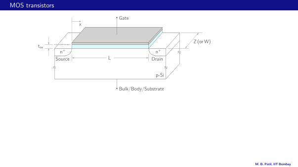
MOS transistors
p-Si
Z (orW)
Gate
Bulk/Body/Substrate
L
x
tox
Source Drain
n+ n+
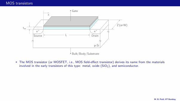
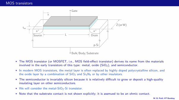
* The MOS transistor (or MOSFET, i.e., MOS field-effect transistor) derives its name from the materialsinvolved in the early transistors of this type: metal, oxide (SiO2), and semiconductor.
* In modern MOS transistors, the metal layer is often replaced by highly doped polycrystalline silicon, andthe oxide layer by a combination of SiO2 and Si3N4 or by other insulators.
* The semiconductor is invariably silicon because it is relatively difficult to grow or deposit a high-qualityinsulating layer on other semiconductors.
* We will consider the metal-SiO2-Si transistor.
* Note that the substrate contact is not shown explicitly; it is assmued to be an ohmic contact.
M. B. Patil, IIT Bombay
MOS transistors
p-Si
Z (orW)
Gate
Bulk/Body/Substrate
L
x
tox
Source Drain
n+ n+
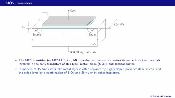
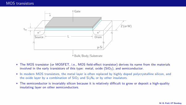
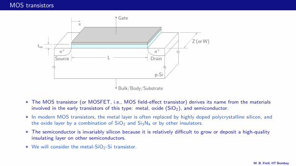
* The MOS transistor (or MOSFET, i.e., MOS field-effect transistor) derives its name from the materialsinvolved in the early transistors of this type: metal, oxide (SiO2), and semiconductor.
* In modern MOS transistors, the metal layer is often replaced by highly doped polycrystalline silicon, andthe oxide layer by a combination of SiO2 and Si3N4 or by other insulators.
* The semiconductor is invariably silicon because it is relatively difficult to grow or deposit a high-qualityinsulating layer on other semiconductors.
* We will consider the metal-SiO2-Si transistor.
* Note that the substrate contact is not shown explicitly; it is assmued to be an ohmic contact.
M. B. Patil, IIT Bombay
MOS transistors
p-Si
Gate
Bulk/Body/Substrate
L
x
MOS transistor
y
Gate
p-Si
metal
oxide
semiconductortox
Bulk/Body/Substrate
MOS capacitor
Source Drain
n+ n+
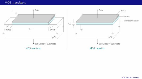
* The heart of a MOS transistor is the MOS capacitor which consists of an insulator (SiO2), with a metalon one side and a semiconductor on the other.
* The oxide thickness tox, which is typically of the order of 100 A (i.e., 0.01µm), is crucial in determiningthe behaviour of the MOS capacitor.
* The metal thickness — typically a few hundred nm — depends on technological considerations, but itsexact value is not important.
M. B. Patil, IIT Bombay
MOS transistors
p-Si
Gate
Bulk/Body/Substrate
L
x
MOS transistor
y
Gate
p-Si
metal
oxide
semiconductortox
Bulk/Body/Substrate
MOS capacitor
Source Drain
n+ n+
* The heart of a MOS transistor is the MOS capacitor which consists of an insulator (SiO2), with a metalon one side and a semiconductor on the other.
* The oxide thickness tox, which is typically of the order of 100 A (i.e., 0.01µm), is crucial in determiningthe behaviour of the MOS capacitor.
* The metal thickness — typically a few hundred nm — depends on technological considerations, but itsexact value is not important.
M. B. Patil, IIT Bombay
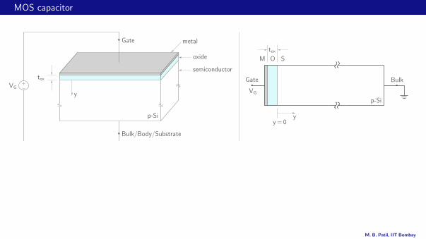
MOS capacitor
p-Si
toxM O S
yy= 0
Gate Bulk
VGy
Gate
p-Si
metal
oxide
semiconductor
Bulk/Body/Substrate
VG
tox
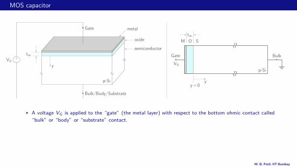
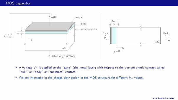
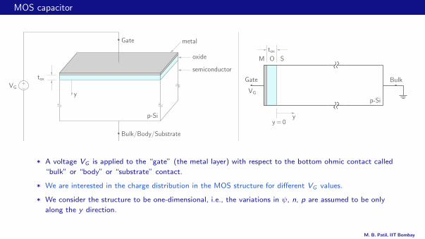
* A voltage VG is applied to the “gate” (the metal layer) with respect to the bottom ohmic contact called
“bulk” or “body” or “substrate” contact.
* We are interested in the charge distribution in the MOS structure for different VG values.
* We consider the structure to be one-dimensional, i.e., the variations in ψ, n, p are assumed to be only
along the y direction.
M. B. Patil, IIT Bombay
MOS capacitor
p-Si
toxM O S
yy= 0
Gate Bulk
VGy
Gate
p-Si
metal
oxide
semiconductor
Bulk/Body/Substrate
VG
tox
* A voltage VG is applied to the “gate” (the metal layer) with respect to the bottom ohmic contact called
“bulk” or “body” or “substrate” contact.
* We are interested in the charge distribution in the MOS structure for different VG values.
* We consider the structure to be one-dimensional, i.e., the variations in ψ, n, p are assumed to be only
along the y direction.
M. B. Patil, IIT Bombay
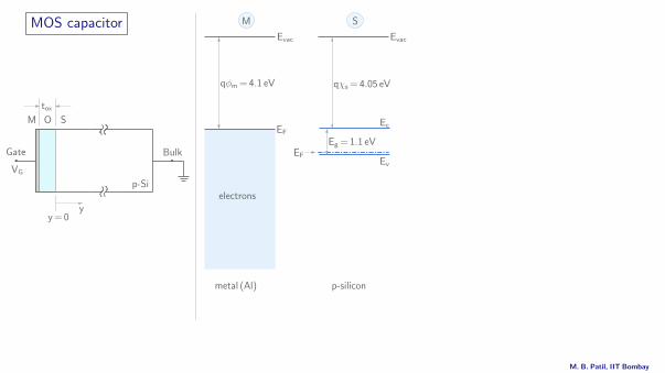
MOS capacitor
p-Si
Bulk
toxM O S
yy= 0
Gate
VG
EF
qφm= 4.1 eV
Eg = 1.1 eV
qχs= 4.05 eV
Ev
EF
Ec
p-siliconmetal (Al)
electrons
M S
Evac Evac
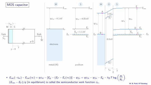
* Metal work function φm: An electron requires energy qφm to make a transition from the Fermi level to the vacuum
level, i.e., to be free of the attractive forces it experiences inside the metal.
M. B. Patil, IIT Bombay

MOS capacitor
p-Si
Bulk
toxM O S
yy= 0
Gate
VG
EF
qφm= 4.1 eV
Eg = 1.1 eV
qχs= 4.05 eV
Ev
EF
Ec
p-siliconmetal (Al)
electrons
M S
Evac Evac
* Metal work function φm: An electron requires energy qφm to make a transition from the Fermi level to the vacuum
level, i.e., to be free of the attractive forces it experiences inside the metal.
M. B. Patil, IIT Bombay

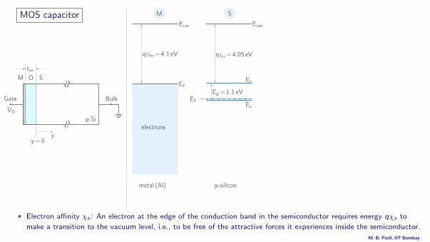
MOS capacitor
p-Si
Bulk
toxM O S
yy= 0
Gate
VG
EF
qφm= 4.1 eV
Eg = 1.1 eV
qχs= 4.05 eV
Ev
EF
Ec
p-siliconmetal (Al)
electrons
M S
Evac Evac
* Electron affinity χs : An electron at the edge of the conduction band in the semiconductor requires energy qχs to
make a transition to the vacuum level, i.e., to be free of the attractive forces it experiences inside the semiconductor.
M. B. Patil, IIT Bombay
MOS capacitor
p-Si
Bulk
toxM O S
yy= 0
Gate
VG
EF
qφm= 4.1 eV
Eg = 1.1 eV
qχs= 4.05 eV
Ev
EF
Ec
p-siliconmetal (Al)
electrons
M S
Evac Evac
qφm
Ec
Ev
EF
1 eV
qχsEoxc
Eoxv
8.8 eV
qφs
Eg
EF
ytox0
M O S
Evac
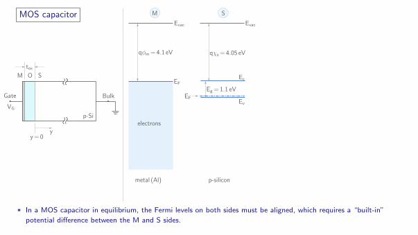
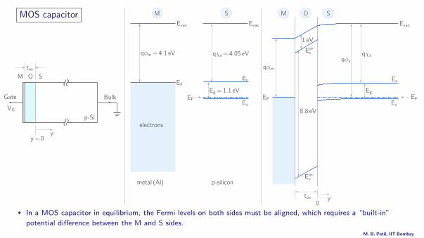
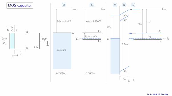
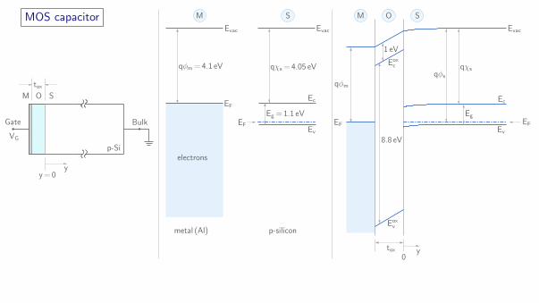
* In a MOS capacitor in equilibrium, the Fermi levels on both sides must be aligned, which requires a “built-in”
potential difference between the M and S sides.
M. B. Patil, IIT Bombay
MOS capacitor
p-Si
Bulk
toxM O S
yy= 0
Gate
VG
EF
qφm= 4.1 eV
Eg = 1.1 eV
qχs= 4.05 eV
Ev
EF
Ec
p-siliconmetal (Al)
electrons
M S
Evac Evac
qφm
Ec
Ev
EF
1 eV
qχsEoxc
Eoxv
8.8 eV
qφs
Eg
EF
ytox0
M O S
Evac
* In a MOS capacitor in equilibrium, the Fermi levels on both sides must be aligned, which requires a “built-in”
potential difference between the M and S sides.
M. B. Patil, IIT Bombay
MOS capacitor
p-Si
Bulk
toxM O S
yy= 0
Gate
VG
EF
qφm= 4.1 eV
qφm
Ec
Ev
EF
1 eV
qχsEoxc
Eoxv
Eg = 1.1 eV
qχs= 4.05 eV
8.8 eV
qφs
Eg
Ev
EF
Ec
EF
p-siliconmetal (Al)
ytox0
electrons
M M OS S
Evac Evac Evac
* In addition to the voltage drop on the semiconductor side, there is a voltage drop across the oxide layer. If there is no
charge in the oxide layer,dEdy
=ρ
εox= 0 → E= constant.
M. B. Patil, IIT Bombay
MOS capacitor
p-Si
Bulk
toxM O S
yy= 0
Gate
VG
EF
qφm= 4.1 eV
qφm
Ec
Ev
EF
1 eV
qχsEoxc
Eoxv
Eg = 1.1 eV
qχs= 4.05 eV
8.8 eV
qφs
Eg
Ev
EF
Ec
EF
p-siliconmetal (Al)
ytox0
electrons
M M OS S
Evac Evac Evac
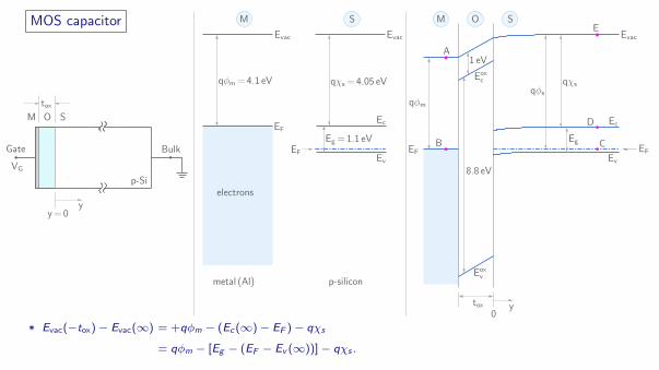
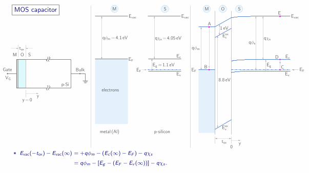
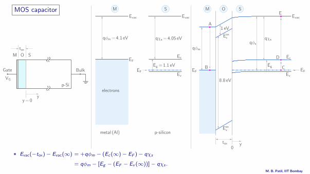
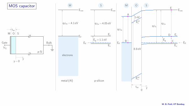
C
A
D
E
B
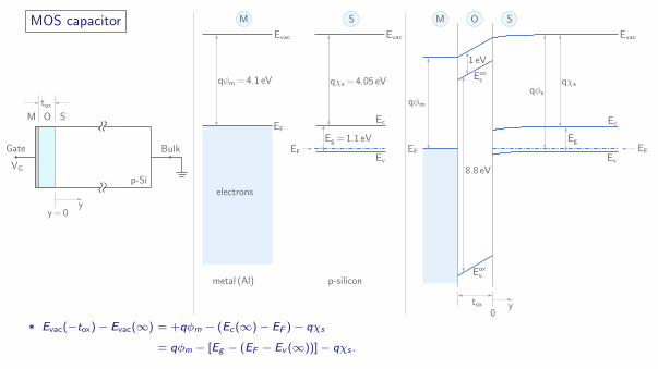
* Evac(−tox)− Evac(∞) = +qφm − (Ec (∞)− EF )− qχs
= qφm − [Eg − (EF − Ev (∞))]− qχs .
M. B. Patil, IIT Bombay
MOS capacitor
p-Si
Bulk
toxM O S
yy= 0
Gate
VG
EF
qφm= 4.1 eV
qφm
Ec
Ev
EF
1 eV
qχsEoxc
Eoxv
Eg = 1.1 eV
qχs= 4.05 eV
8.8 eV
qφs
Eg
Ev
EF
Ec
EF
p-siliconmetal (Al)
ytox0
electrons
M M OS S
Evac Evac Evac
C
A
D
E
B
* Evac(−tox)− Evac(∞) = +qφm − (Ec (∞)− EF )− qχs
= qφm − [Eg − (EF − Ev (∞))]− qχs .
M. B. Patil, IIT Bombay
MOS capacitor
p-Si
Bulk
toxM O S
yy= 0
Gate
VG
EF
qφm= 4.1 eV
qφm
Ec
Ev
EF
1 eV
qχsEoxc
Eoxv
Eg = 1.1 eV
qχs= 4.05 eV
8.8 eV
qφs
Eg
Ev
EF
Ec
EF
p-siliconmetal (Al)
ytox0
electrons
M M OS S
Evac Evac Evac
C
A
D
E
B
* Evac(−tox)− Evac(∞) = +qφm − (Ec (∞)− EF )− qχs
= qφm − [Eg − (EF − Ev (∞))]− qχs .M. B. Patil, IIT Bombay
MOS capacitor
p-Si
Bulk
toxM O S
yy= 0
Gate
VG
EF
EF
qφm= 4.1 eV
qφm
Ec
Ev
EF
1 eV
qχs
C
A
D
E
B
Eoxc
Eoxv
Eg = 1.1 eV
qχs= 4.05 eV
8.8 eV
qφs
Eg
Ev
EF
Ec
p-siliconmetal (Al)
ytox0
electrons
M M OS S
Evac Evac Evac
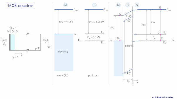
* Evac(−tox)− Evac(∞) = qφm − [Eg − (EF − Ev (∞))]− qχs = qφm − qχs − Eg − kBT log
(p0
Nv
).
(Evac − EF )/q (in equilibrium) is called the semiconductor work function φs .
M. B. Patil, IIT Bombay
MOS capacitor
p-Si
Bulk
toxM O S
yy= 0
Gate
VG
EF
EF
qφm= 4.1 eV
qφm
Ec
Ev
EF
1 eV
qχs
C
A
D
E
B
Eoxc
Eoxv
Eg = 1.1 eV
qχs= 4.05 eV
8.8 eV
qφs
Eg
Ev
EF
Ec
p-siliconmetal (Al)
ytox0
electrons
M M OS S
Evac Evac Evac
* Evac(−tox)− Evac(∞) = qφm − [Eg − (EF − Ev (∞))]− qχs = qφm − qχs − Eg − kBT log
(p0
Nv
).
(Evac − EF )/q (in equilibrium) is called the semiconductor work function φs .M. B. Patil, IIT Bombay
MOS capacitor
p-Si
Bulk
toxM O S
yy= 0
Gate
VG
EF
EF
qφm= 4.1 eV
qφm
Ec
Ev
EF
1 eV
qχs
C
A
D
E
B
Eoxc
Eoxv
Eg = 1.1 eV
qχs= 4.05 eV
8.8 eV
qφs
Eg
Ev
EF
Ec
p-siliconmetal (Al)
ytox0
electrons
M M OS S
Evac Evac Evac
* The built-in potential difference can also be expressed as
Evac(−tox)− Evac(∞) = q(φm − φs) ≡ qφms . (Note that φs depends on the doping density.)
M. B. Patil, IIT Bombay
MOS capacitor
p-Si
Bulk
toxM O S
yy= 0
Gate
VG
EF
EF
qφm= 4.1 eV
qφm
Ec
Ev
EF
1 eV
qχs
C
A
D
E
B
Eoxc
Eoxv
Eg = 1.1 eV
qχs= 4.05 eV
8.8 eV
qφs
Eg
Ev
EF
Ec
p-siliconmetal (Al)
ytox0
electrons
M M OS S
Evac Evac Evac
* The built-in potential difference can also be expressed as
Evac(−tox)− Evac(∞) = q(φm − φs) ≡ qφms . (Note that φs depends on the doping density.)M. B. Patil, IIT Bombay
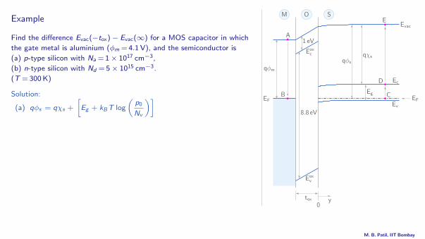
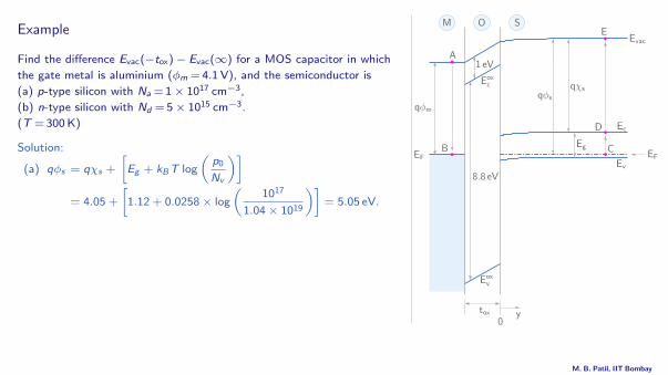
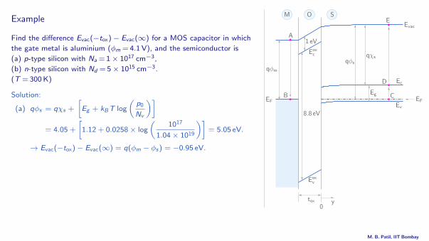
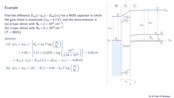
Example
EF
qφm
Ec
Ev
EF
1 eV
qχs
C
A
D
E
B
Eoxc
Eoxv
8.8 eV
qφs
Eg
ytox0
M O S
Evac
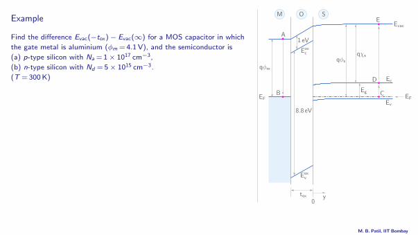
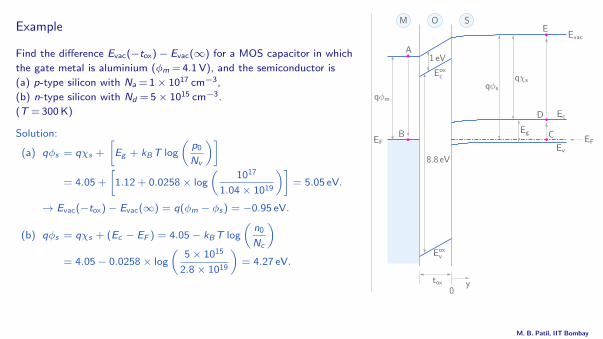
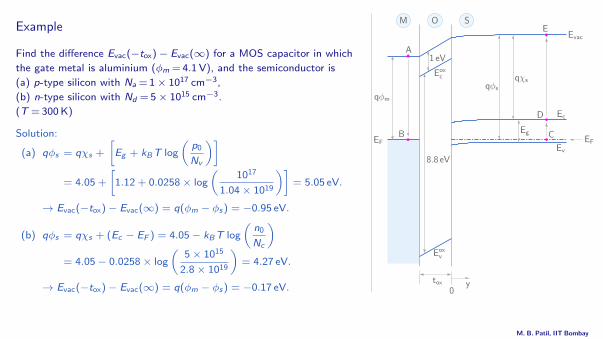
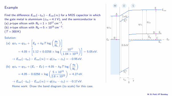
Find the difference Evac(−tox)− Evac(∞) for a MOS capacitor in which
the gate metal is aluminium (φm = 4.1 V), and the semiconductor is
(a) p-type silicon with Na = 1× 1017 cm−3,
(b) n-type silicon with Nd = 5× 1015 cm−3.
(T = 300 K)
Solution:
(a) qφs = qχs +
[Eg + kBT log
(p0
Nv
)]= 4.05 +
[1.12 + 0.0258× log
(1017
1.04× 10¹⁹
)]= 5.05 eV.
→ Evac(−tox)− Evac(∞) = q(φm − φs) = −0.95 eV.
(b) qφs = qχs + (Ec − EF ) = 4.05− kBT log
(n0
Nc
)= 4.05− 0.0258× log
(5× 10¹⁵
2.8× 10¹⁹
)= 4.27 eV.
→ Evac(−tox)− Evac(∞) = q(φm − φs) = −0.17 eV.
Home work: Draw the band diagram (to scale) for this case.
M. B. Patil, IIT Bombay
Example
EF
qφm
Ec
Ev
EF
1 eV
qχs
C
A
D
E
B
Eoxc
Eoxv
8.8 eV
qφs
Eg
ytox0
M O S
Evac
Find the difference Evac(−tox)− Evac(∞) for a MOS capacitor in which
the gate metal is aluminium (φm = 4.1 V), and the semiconductor is
(a) p-type silicon with Na = 1× 1017 cm−3,
(b) n-type silicon with Nd = 5× 1015 cm−3.
(T = 300 K)
Solution:
(a) qφs = qχs +
[Eg + kBT log
(p0
Nv
)]
= 4.05 +
[1.12 + 0.0258× log
(1017
1.04× 10¹⁹
)]= 5.05 eV.
→ Evac(−tox)− Evac(∞) = q(φm − φs) = −0.95 eV.
(b) qφs = qχs + (Ec − EF ) = 4.05− kBT log
(n0
Nc
)= 4.05− 0.0258× log
(5× 10¹⁵
2.8× 10¹⁹
)= 4.27 eV.
→ Evac(−tox)− Evac(∞) = q(φm − φs) = −0.17 eV.
Home work: Draw the band diagram (to scale) for this case.
M. B. Patil, IIT Bombay
Example
EF
qφm
Ec
Ev
EF
1 eV
qχs
C
A
D
E
B
Eoxc
Eoxv
8.8 eV
qφs
Eg
ytox0
M O S
Evac
Find the difference Evac(−tox)− Evac(∞) for a MOS capacitor in which
the gate metal is aluminium (φm = 4.1 V), and the semiconductor is
(a) p-type silicon with Na = 1× 1017 cm−3,
(b) n-type silicon with Nd = 5× 1015 cm−3.
(T = 300 K)
Solution:
(a) qφs = qχs +
[Eg + kBT log
(p0
Nv
)]= 4.05 +
[1.12 + 0.0258× log
(1017
1.04× 10¹⁹
)]= 5.05 eV.
→ Evac(−tox)− Evac(∞) = q(φm − φs) = −0.95 eV.
(b) qφs = qχs + (Ec − EF ) = 4.05− kBT log
(n0
Nc
)= 4.05− 0.0258× log
(5× 10¹⁵
2.8× 10¹⁹
)= 4.27 eV.
→ Evac(−tox)− Evac(∞) = q(φm − φs) = −0.17 eV.
Home work: Draw the band diagram (to scale) for this case.
M. B. Patil, IIT Bombay
Example
EF
qφm
Ec
Ev
EF
1 eV
qχs
C
A
D
E
B
Eoxc
Eoxv
8.8 eV
qφs
Eg
ytox0
M O S
Evac
Find the difference Evac(−tox)− Evac(∞) for a MOS capacitor in which
the gate metal is aluminium (φm = 4.1 V), and the semiconductor is
(a) p-type silicon with Na = 1× 1017 cm−3,
(b) n-type silicon with Nd = 5× 1015 cm−3.
(T = 300 K)
Solution:
(a) qφs = qχs +
[Eg + kBT log
(p0
Nv
)]= 4.05 +
[1.12 + 0.0258× log
(1017
1.04× 10¹⁹
)]= 5.05 eV.
→ Evac(−tox)− Evac(∞) = q(φm − φs) = −0.95 eV.
(b) qφs = qχs + (Ec − EF ) = 4.05− kBT log
(n0
Nc
)
= 4.05− 0.0258× log
(5× 10¹⁵
2.8× 10¹⁹
)= 4.27 eV.
→ Evac(−tox)− Evac(∞) = q(φm − φs) = −0.17 eV.
Home work: Draw the band diagram (to scale) for this case.
M. B. Patil, IIT Bombay
Example
EF
qφm
Ec
Ev
EF
1 eV
qχs
C
A
D
E
B
Eoxc
Eoxv
8.8 eV
qφs
Eg
ytox0
M O S
Evac
Find the difference Evac(−tox)− Evac(∞) for a MOS capacitor in which
the gate metal is aluminium (φm = 4.1 V), and the semiconductor is
(a) p-type silicon with Na = 1× 1017 cm−3,
(b) n-type silicon with Nd = 5× 1015 cm−3.
(T = 300 K)
Solution:
(a) qφs = qχs +
[Eg + kBT log
(p0
Nv
)]= 4.05 +
[1.12 + 0.0258× log
(1017
1.04× 10¹⁹
)]= 5.05 eV.
→ Evac(−tox)− Evac(∞) = q(φm − φs) = −0.95 eV.
(b) qφs = qχs + (Ec − EF ) = 4.05− kBT log
(n0
Nc
)= 4.05− 0.0258× log
(5× 10¹⁵
2.8× 10¹⁹
)= 4.27 eV.
→ Evac(−tox)− Evac(∞) = q(φm − φs) = −0.17 eV.
Home work: Draw the band diagram (to scale) for this case.
M. B. Patil, IIT Bombay
Example
EF
qφm
Ec
Ev
EF
1 eV
qχs
C
A
D
E
B
Eoxc
Eoxv
8.8 eV
qφs
Eg
ytox0
M O S
Evac
Find the difference Evac(−tox)− Evac(∞) for a MOS capacitor in which
the gate metal is aluminium (φm = 4.1 V), and the semiconductor is
(a) p-type silicon with Na = 1× 1017 cm−3,
(b) n-type silicon with Nd = 5× 1015 cm−3.
(T = 300 K)
Solution:
(a) qφs = qχs +
[Eg + kBT log
(p0
Nv
)]= 4.05 +
[1.12 + 0.0258× log
(1017
1.04× 10¹⁹
)]= 5.05 eV.
→ Evac(−tox)− Evac(∞) = q(φm − φs) = −0.95 eV.
(b) qφs = qχs + (Ec − EF ) = 4.05− kBT log
(n0
Nc
)= 4.05− 0.0258× log
(5× 10¹⁵
2.8× 10¹⁹
)= 4.27 eV.
→ Evac(−tox)− Evac(∞) = q(φm − φs) = −0.17 eV.
Home work: Draw the band diagram (to scale) for this case.
M. B. Patil, IIT Bombay
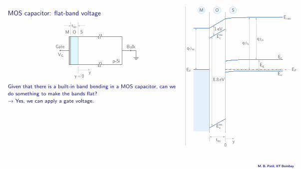
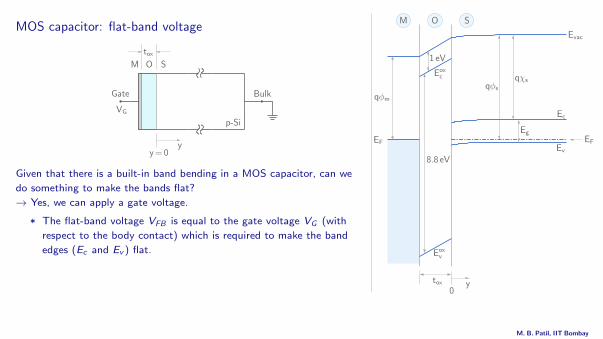
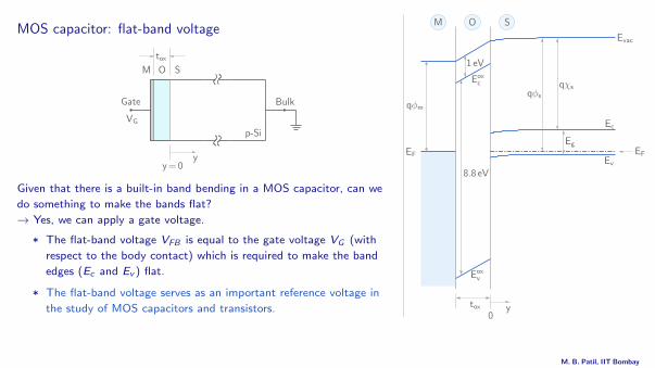
MOS capacitor: flat-band voltage
p-Si
Bulk
toxM O S
yy= 0
Gate
VG
qφm
Ec
Ev
EF
1 eV
qχsEoxc
Eoxv
8.8 eV
qφs
Eg
EF
ytox0
M O S
Evac
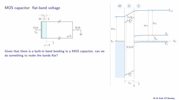
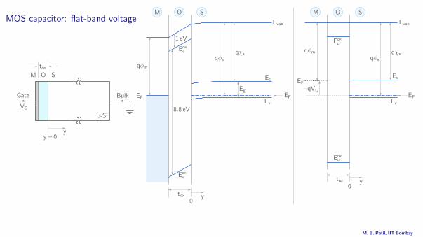
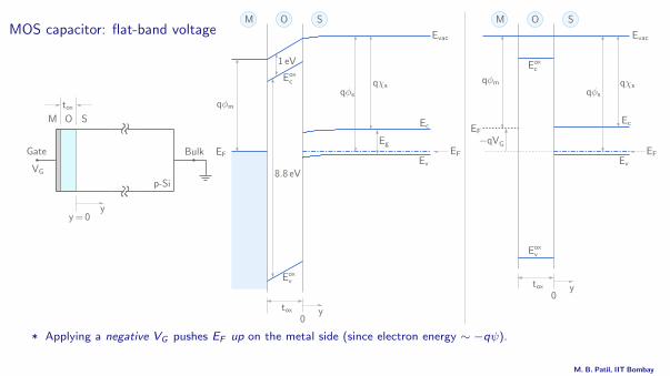
Given that there is a built-in band bending in a MOS capacitor, can we
do something to make the bands flat?
→ Yes, we can apply a gate voltage.
* The flat-band voltage VFB is equal to the gate voltage VG (with
respect to the body contact) which is required to make the band
edges (Ec and Ev ) flat.
* The flat-band voltage serves as an important reference voltage in
the study of MOS capacitors and transistors.
M. B. Patil, IIT Bombay
MOS capacitor: flat-band voltage
p-Si
Bulk
toxM O S
yy= 0
Gate
VG
qφm
Ec
Ev
EF
1 eV
qχsEoxc
Eoxv
8.8 eV
qφs
Eg
EF
ytox0
M O S
Evac
Given that there is a built-in band bending in a MOS capacitor, can we
do something to make the bands flat?
→ Yes, we can apply a gate voltage.
* The flat-band voltage VFB is equal to the gate voltage VG (with
respect to the body contact) which is required to make the band
edges (Ec and Ev ) flat.
* The flat-band voltage serves as an important reference voltage in
the study of MOS capacitors and transistors.
M. B. Patil, IIT Bombay
qφm
Ec
Ev
EF
1 eV
qχsEoxc
Eoxv
8.8 eV
qφs
Eg
EF
ytox0
M O S
Evac
Eoxv
Eoxc
−qVG
qφm
Ev
EF
EcEF
ytox0
M O S
Evac
qφs
qχs
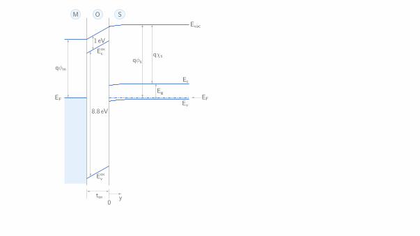
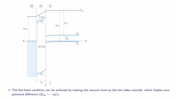
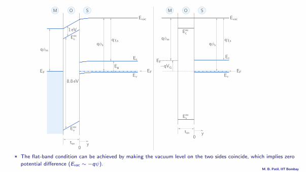
* The flat-band condition can be achieved by making the vacuum level on the two sides coincide, which implies zero
potential difference (Evac ∼ −qψ).
M. B. Patil, IIT Bombay
qφm
Ec
Ev
EF
1 eV
qχsEoxc
Eoxv
8.8 eV
qφs
Eg
EF
ytox0
M O S
Evac
Eoxv
Eoxc
−qVG
qφm
Ev
EF
EcEF
ytox0
M O S
Evac
qφs
qχs
* The flat-band condition can be achieved by making the vacuum level on the two sides coincide, which implies zero
potential difference (Evac ∼ −qψ).
M. B. Patil, IIT Bombay
qφm
Ec
Ev
EF
1 eV
qχsEoxc
Eoxv
8.8 eV
qφs
Eg
EF
ytox0
M O S
Evac
Eoxv
Eoxc
−qVG
qφm
Ev
EF
EcEF
ytox0
M O S
Evac
qφs
qχs
* The flat-band condition can be achieved by making the vacuum level on the two sides coincide, which implies zero
potential difference (Evac ∼ −qψ).M. B. Patil, IIT Bombay
MOS capacitor: flat-band voltage
Eoxv
Eoxc
−qVG
qφm
Ev
EF
EcEF
qφm
Ec
Ev
EF
1 eV
qχsEoxc
Eoxv
8.8 eV
qφs
Eg
EF
p-Si
Bulk
toxM O S
yy= 0
Gate
VG
ytox0
ytox0
MM OO SS
EvacEvac
qφs
qχs
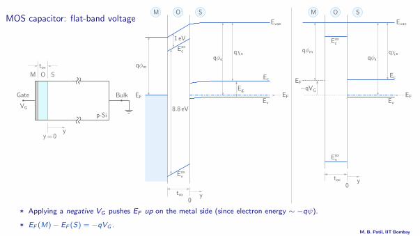
* Applying a negative VG pushes EF up on the metal side (since electron energy ∼ −qψ).
* EF (M)− EF (S) = −qVG .
M. B. Patil, IIT Bombay
MOS capacitor: flat-band voltage
Eoxv
Eoxc
−qVG
qφm
Ev
EF
EcEF
qφm
Ec
Ev
EF
1 eV
qχsEoxc
Eoxv
8.8 eV
qφs
Eg
EF
p-Si
Bulk
toxM O S
yy= 0
Gate
VG
ytox0
ytox0
MM OO SS
EvacEvac
qφs
qχs
* Applying a negative VG pushes EF up on the metal side (since electron energy ∼ −qψ).
* EF (M)− EF (S) = −qVG .M. B. Patil, IIT Bombay
MOS capacitor: flat-band voltage
Eoxv
Eoxc
−qVG
qφm
Ev
EF
EcEF
qφm
Ec
Ev
EF
1 eV
qχsEoxc
Eoxv
8.8 eV
qφs
Eg
EF
p-Si
Bulk
toxM O S
yy= 0
Gate
VG
ytox0
ytox0
MM OO SS
EvacEvac
qφs
qχs
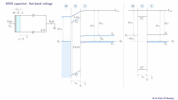
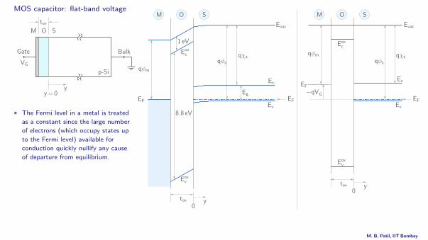
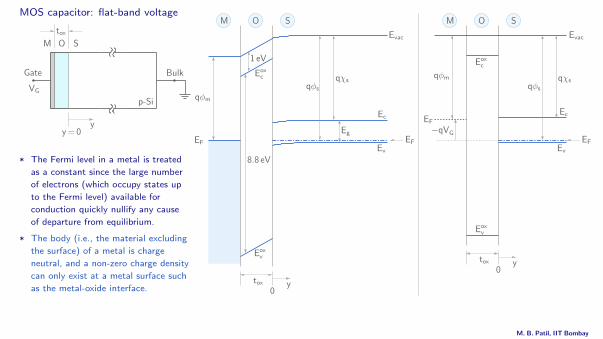
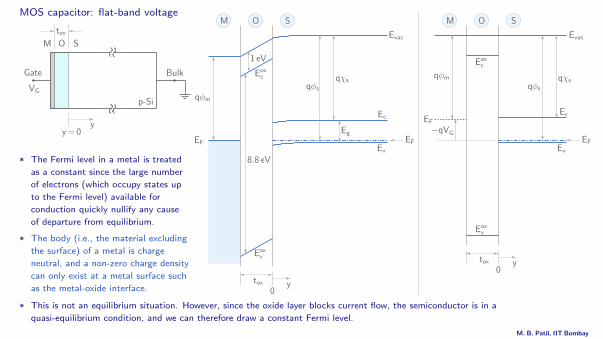
* The Fermi level in a metal is treated
as a constant since the large number
of electrons (which occupy states up
to the Fermi level) available for
conduction quickly nullify any cause
of departure from equilibrium.
* The body (i.e., the material excluding
the surface) of a metal is charge
neutral, and a non-zero charge density
can only exist at a metal surface such
as the metal-oxide interface.
* This is not an equilibrium situation. However, since the oxide layer blocks current flow, the semiconductor is in a
quasi-equilibrium condition, and we can therefore draw a constant Fermi level.
M. B. Patil, IIT Bombay
MOS capacitor: flat-band voltage
Eoxv
Eoxc
−qVG
qφm
Ev
EF
EcEF
qφm
Ec
Ev
EF
1 eV
qχsEoxc
Eoxv
8.8 eV
qφs
Eg
EF
p-Si
Bulk
toxM O S
yy= 0
Gate
VG
ytox0
ytox0
MM OO SS
EvacEvac
qφs
qχs
* The Fermi level in a metal is treated
as a constant since the large number
of electrons (which occupy states up
to the Fermi level) available for
conduction quickly nullify any cause
of departure from equilibrium.
* The body (i.e., the material excluding
the surface) of a metal is charge
neutral, and a non-zero charge density
can only exist at a metal surface such
as the metal-oxide interface.
* This is not an equilibrium situation. However, since the oxide layer blocks current flow, the semiconductor is in a
quasi-equilibrium condition, and we can therefore draw a constant Fermi level.
M. B. Patil, IIT Bombay
MOS capacitor
p-Si
Bulk
toxM O S
yy= 0
Gate
VG
M O
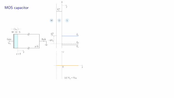
(a) VG=VFB
S
ψ
y0
EF
Ev
Ec
0
Eoxc
EMF
y
−qVG
M O
(b) VG>VFB
S
ψ
y y0
0
Eoxc
−qVGEF
Ev
y
EMF
Ec
M O
(c) VG<VFB
S
ψ
y0
−qVG
EF
Ev
Ec
0
Eoxc
EMF
y
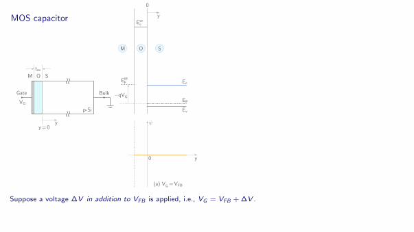
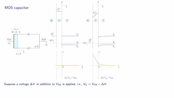
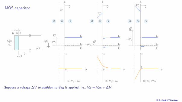
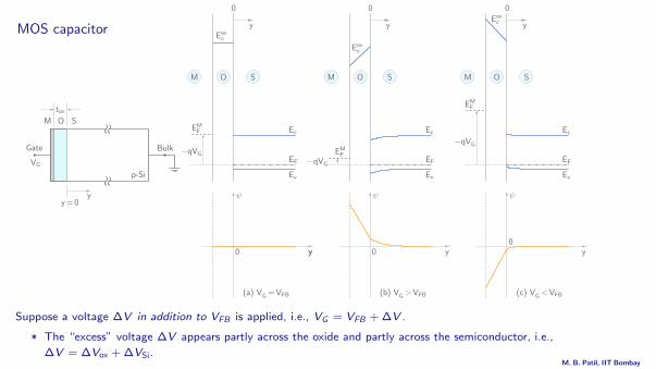
Suppose a voltage ∆V in addition to VFB is applied, i.e., VG = VFB + ∆V .
* The “excess” voltage ∆V appears partly across the oxide and partly across the semiconductor, i.e.,
∆V = ∆Vox + ∆VSi.
M. B. Patil, IIT Bombay
MOS capacitor
p-Si
Bulk
toxM O S
yy= 0
Gate
VG
M O
(a) VG=VFB
S
ψ
y0
EF
Ev
Ec
0
Eoxc
EMF
y
−qVG
M O
(b) VG>VFB
S
ψ
y y0
0
Eoxc
−qVGEF
Ev
y
EMF
Ec
M O
(c) VG<VFB
S
ψ
y0
−qVG
EF
Ev
Ec
0
Eoxc
EMF
y
Suppose a voltage ∆V in addition to VFB is applied, i.e., VG = VFB + ∆V .
* The “excess” voltage ∆V appears partly across the oxide and partly across the semiconductor, i.e.,
∆V = ∆Vox + ∆VSi.M. B. Patil, IIT Bombay

MOS capacitor
p-Si
Bulk
toxM O S
yy= 0
Gate
VG
M M MO O O
(a) VG=VFB (b) VG>VFB (c) VG<VFB
S S S
ψ ψ ψ
yy y0 00
EF
Ev
Ec
−qVG
EF
Ev
Ec
0 0 0
Eoxc
Eoxc
−qVG
Eoxc
EF
Ev
EcEMF
EMF
y y y
EMF−qVG
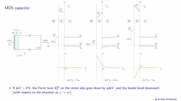
* If ∆V > 0 V, the Fermi level EMF on the metal side goes down by q∆V , and the bands bend downward
(with respect to the situation at y →∞).
M. B. Patil, IIT Bombay
MOS capacitor
p-Si
Bulk
toxM O S
yy= 0
Gate
VG
M M MO O O
(a) VG=VFB (b) VG>VFB (c) VG<VFB
S S S
ψ ψ ψ
yy y0 00
EF
Ev
Ec
−qVG
EF
Ev
Ec
0 0 0
Eoxc
Eoxc
−qVG
Eoxc
EF
Ev
EcEMF
EMF
y y y
EMF−qVG
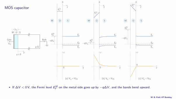
* If ∆V < 0 V, the Fermi level EMF on the metal side goes up by −q∆V , and the bands bend upward.
M. B. Patil, IIT Bombay
MOS capacitor
p-Si
Bulk
toxM O S
yy= 0
Gate
VG
M M MO O O
(a) VG=VFB (b) VG>VFB (c) VG<VFB
S S S
ψ ψ ψ
yy y0 00
EF
Ev
Ec
−qVG
EF
Ev
Ec
0 0 0
Eoxc
Eoxc
−qVG
Eoxc
EF
Ev
EcEMF
EMF
y y y
EMF−qVG
* If ∆V < 0 V, the Fermi level EMF on the metal side goes up by −q∆V , and the bands bend upward.
M. B. Patil, IIT Bombay

MOS capacitor
p-Si
Bulk
toxM O S
yy= 0
Gate
VG
M M MO O O
(a) VG=VFB (b) VG>VFB (c) VG<VFB
S S S
ψ ψ ψ
yy y0 00
EF
Ev
Ec
−qVG
EF
Ev
Ec
0 0 0
Eoxc
Eoxc
−qVG
Eoxc
EF
Ev
EcEMF
EMF
y y y
EMF−qVG
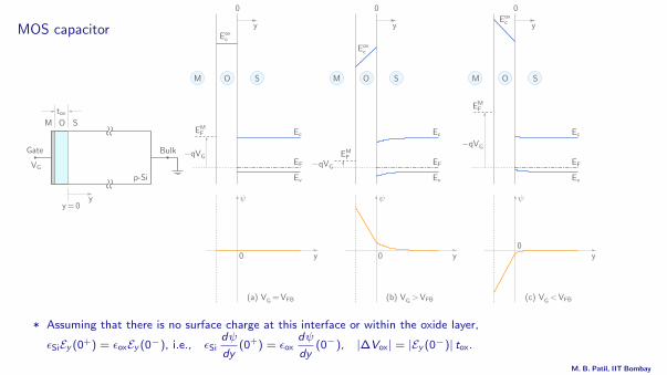
* Assuming that there is no surface charge at this interface or within the oxide layer,
εSiEy (0+) = εoxEy (0−), i.e., εSidψ
dy(0+) = εox
dψ
dy(0−), |∆Vox| = |Ey (0−)| tox.
M. B. Patil, IIT Bombay
MOS capacitor
p-Si
Bulk
toxM O S
yy= 0
Gate
VG
M M MO O O
(a) VG=VFB (b) VG>VFB (c) VG<VFB
S S S
ψ ψ ψ
yy y0 00
EF
Ev
Ec
−qVG
EF
Ev
Ec
0 0 0
Eoxc
Eoxc
−qVG
Eoxc
EF
Ev
EcEMF
EMF
y y y
EMF−qVG
* Assuming that there is no surface charge at this interface or within the oxide layer,
εSiEy (0+) = εoxEy (0−), i.e., εSidψ
dy(0+) = εox
dψ
dy(0−), |∆Vox| = |Ey (0−)| tox.
M. B. Patil, IIT Bombay

MOS capacitor
p-Si
Bulk
toxM O S
yy= 0
Gate
VG
M M MO O O
(a) VG=VFB (b) VG>VFB (c) VG<VFB
S S S
ψ ψ ψ
yy y0 00
EF
Ev
Ec
−qVG
EF
Ev
Ec
0 0 0
Eoxc
Eoxc
−qVG
Eoxc
EF
Ev
EcEMF
EMF
y y y
EMF−qVG
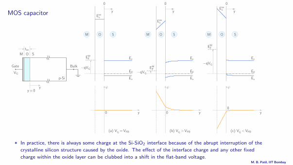
* In practice, there is always some charge at the Si-SiO2 interface because of the abrupt interruption of the
crystalline silicon structure caused by the oxide. The effect of the interface charge and any other fixed
charge within the oxide layer can be clubbed into a shift in the flat-band voltage.
M. B. Patil, IIT Bombay
MOS capacitor
p-Si
Bulk
toxM O S
yy= 0
Gate
VG
M M MO O O
(a) VG=VFB (b) VG>VFB (c) VG<VFB
S S S
ψ ψ ψ
yy y0 00
EF
Ev
Ec
−qVG
EF
Ev
Ec
0 0 0
Eoxc
Eoxc
−qVG
Eoxc
EF
Ev
EcEMF
EMF
y y y
EMF−qVG
* In practice, there is always some charge at the Si-SiO2 interface because of the abrupt interruption of the
crystalline silicon structure caused by the oxide. The effect of the interface charge and any other fixed
charge within the oxide layer can be clubbed into a shift in the flat-band voltage.M. B. Patil, IIT Bombay
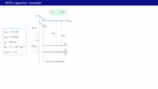
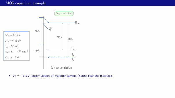
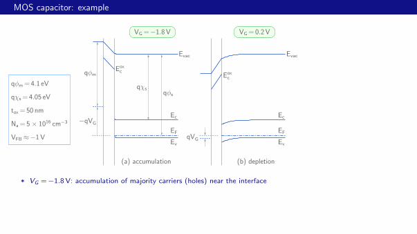
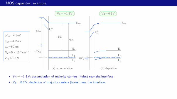
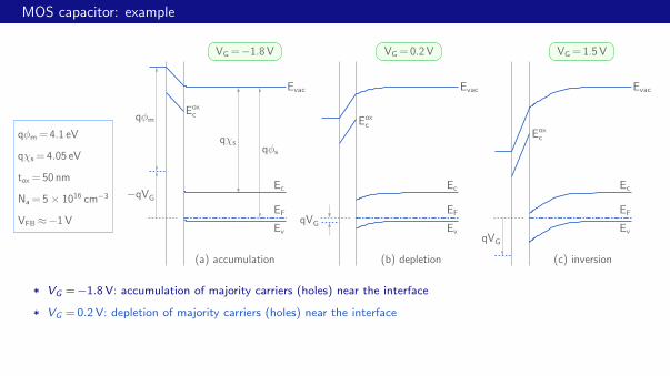
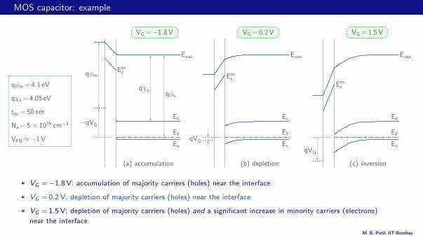
MOS capacitor: example
Ec
EF
Ev
Eoxc
(a) accumulation
qφm
qφm= 4.1 eV
qχs= 4.05 eV
tox= 50 nm
Na= 5× 1016 cm−3
VFB ≈−1V
VG=−1.8 V
Evac
−qVG
qφs
qχs
Ec
EF
Ev
Eoxc
(b) depletion
VG = 0.2 V
Evac
qVG
Ec
EF
Ev
Eoxc
(c) inversion
VG = 1.5 V
Evac
qVG
* VG =−1.8 V: accumulation of majority carriers (holes) near the interface
* VG = 0.2 V: depletion of majority carriers (holes) near the interface
* VG = 1.5 V: depletion of majority carriers (holes) and a significant increase in minority carriers (electrons)
near the interface
M. B. Patil, IIT Bombay

MOS capacitor: accumulation (p-type semiconductor)
qφm= 4.1 eV
qχs= 4.05 eV
tox= 50 nm
Na= 5× 1016 cm−3
y
ψ
ρ
y
y
Ey
0
0
0
y
EF
Ev
Ei
Ec−qVG
QM
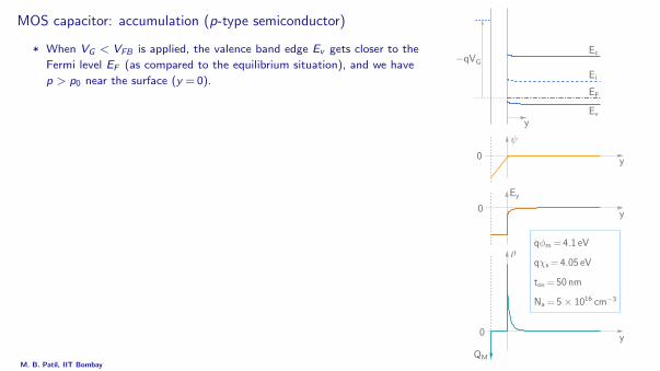
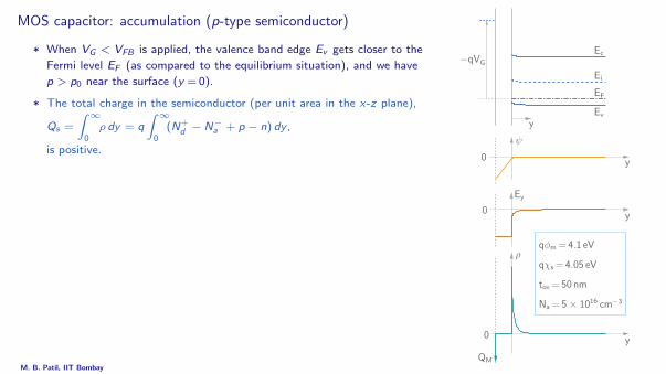
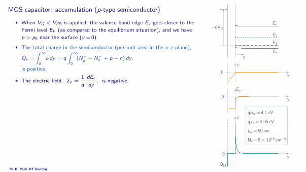
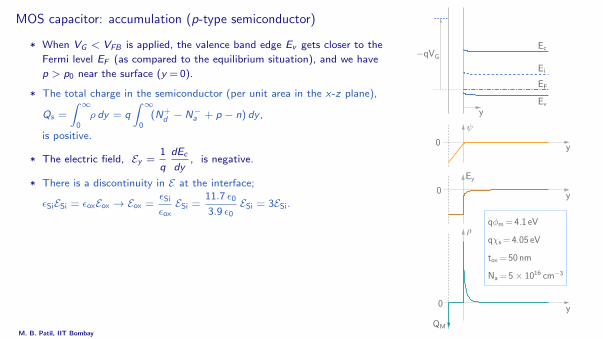
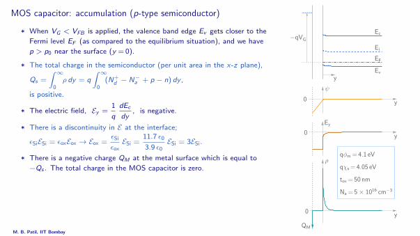
* When VG < VFB is applied, the valence band edge Ev gets closer to the
Fermi level EF (as compared to the equilibrium situation), and we have
p > p0 near the surface (y = 0).
* The total charge in the semiconductor (per unit area in the x-z plane),
Qs =
∫ ∞0ρ dy = q
∫ ∞0
(N+d − N−a + p − n) dy ,
is positive.
* The electric field, Ey =1
q
dEc
dy, is negative.
* There is a discontinuity in E at the interface;
εSiESi = εoxEox → Eox =εSi
εoxESi =
11.7 ε0
3.9 ε0ESi = 3ESi.
* There is a negative charge QM at the metal surface which is equal to
−Qs . The total charge in the MOS capacitor is zero.
M. B. Patil, IIT Bombay
MOS capacitor: accumulation (p-type semiconductor)
qφm= 4.1 eV
qχs= 4.05 eV
tox= 50 nm
Na= 5× 1016 cm−3
y
ψ
ρ
y
y
Ey
0
0
0
y
EF
Ev
Ei
Ec−qVG
QM
* When VG < VFB is applied, the valence band edge Ev gets closer to the
Fermi level EF (as compared to the equilibrium situation), and we have
p > p0 near the surface (y = 0).
* The total charge in the semiconductor (per unit area in the x-z plane),
Qs =
∫ ∞0ρ dy = q
∫ ∞0
(N+d − N−a + p − n) dy ,
is positive.
* The electric field, Ey =1
q
dEc
dy, is negative.
* There is a discontinuity in E at the interface;
εSiESi = εoxEox → Eox =εSi
εoxESi =
11.7 ε0
3.9 ε0ESi = 3ESi.
* There is a negative charge QM at the metal surface which is equal to
−Qs . The total charge in the MOS capacitor is zero.
M. B. Patil, IIT Bombay
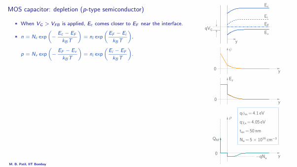
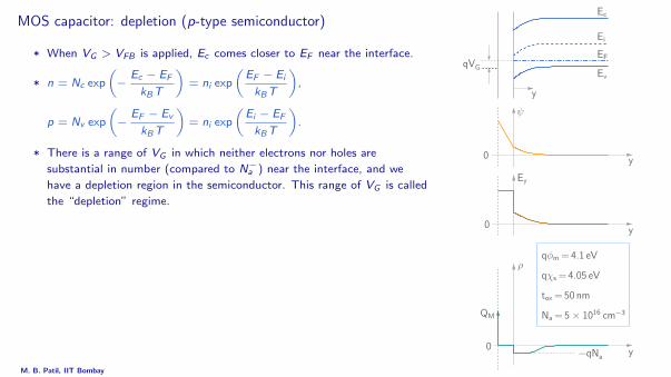
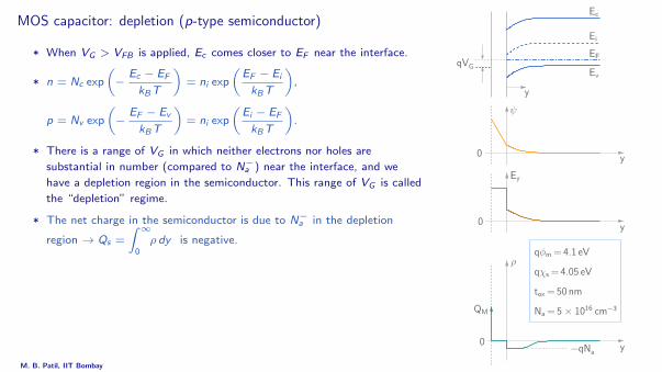
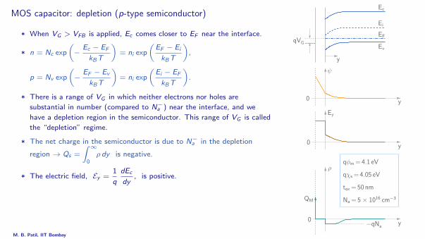
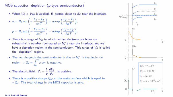
MOS capacitor: depletion (p-type semiconductor)
qφm= 4.1 eV
qχs= 4.05 eV
tox= 50 nm
Na= 5× 1016 cm−3
−qNa
ψ
y
Ey
y
ρ
y
0
0
0
y
EF
Ev
Ei
Ec
qVG
QM
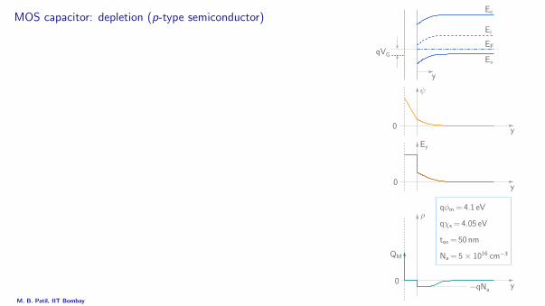
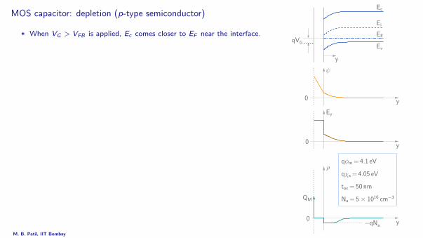
* When VG > VFB is applied, Ec comes closer to EF near the interface.
* n = Nc exp
(− Ec − EF
kBT
)= ni exp
(EF − Ei
kBT
),
p = Nv exp
(− EF − Ev
kBT
)= ni exp
(Ei − EF
kBT
).
* There is a range of VG in which neither electrons nor holes are
substantial in number (compared to N−a ) near the interface, and we
have a depletion region in the semiconductor. This range of VG is called
the “depletion” regime.
* The net charge in the semiconductor is due to N−a in the depletion
region → Qs =
∫ ∞0ρ dy is negative.
* The electric field, Ey =1
q
dEc
dy, is positive.
* There is a positive charge QM at the metal surface which is equal to
−Qs . The total charge in the MOS capacitor is zero.
M. B. Patil, IIT Bombay
MOS capacitor: depletion (p-type semiconductor)
qφm= 4.1 eV
qχs= 4.05 eV
tox= 50 nm
Na= 5× 1016 cm−3
−qNa
ψ
y
Ey
y
ρ
y
0
0
0
y
EF
Ev
Ei
Ec
qVG
QM
* When VG > VFB is applied, Ec comes closer to EF near the interface.
* n = Nc exp
(− Ec − EF
kBT
)= ni exp
(EF − Ei
kBT
),
p = Nv exp
(− EF − Ev
kBT
)= ni exp
(Ei − EF
kBT
).
* There is a range of VG in which neither electrons nor holes are
substantial in number (compared to N−a ) near the interface, and we
have a depletion region in the semiconductor. This range of VG is called
the “depletion” regime.
* The net charge in the semiconductor is due to N−a in the depletion
region → Qs =
∫ ∞0ρ dy is negative.
* The electric field, Ey =1
q
dEc
dy, is positive.
* There is a positive charge QM at the metal surface which is equal to
−Qs . The total charge in the MOS capacitor is zero.
M. B. Patil, IIT Bombay
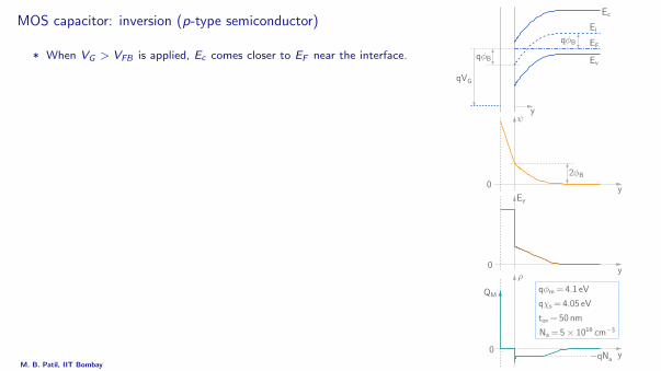
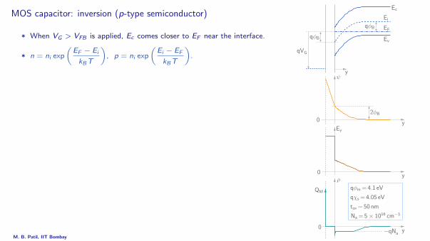
MOS capacitor: inversion (p-type semiconductor)
Na = 5× 1016 cm−3
tox= 50 nm
qχs= 4.05 eV
qφm= 4.1 eV
y
Ey
y
ρ
−qNa
ψ
y
0
0
0
EF
Ev
Ei
qVG
qφB
qφB
y
Ec
2φB
QM
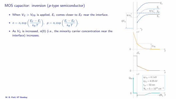
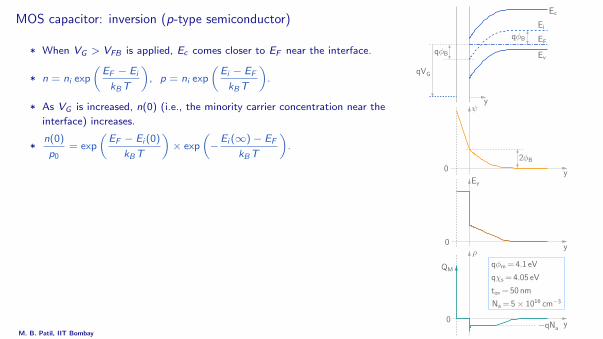
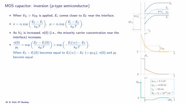
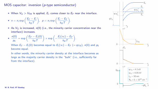
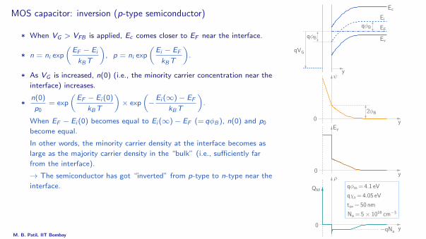
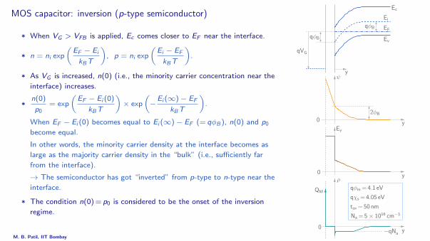
* When VG > VFB is applied, Ec comes closer to EF near the interface.
* n = ni exp
(EF − Ei
kBT
), p = ni exp
(Ei − EF
kBT
).
* As VG is increased, n(0) (i.e., the minority carrier concentration near the
interface) increases.
*n(0)
p0= exp
(EF − Ei (0)
kBT
)× exp
(−Ei (∞)− EF
kBT
).
When EF − Ei (0) becomes equal to Ei (∞)− EF (= qφB), n(0) and p0
become equal.
In other words, the minority carrier density at the interface becomes as
large as the majority carrier density in the “bulk” (i.e., sufficiently far
from the interface).
→ The semiconductor has got “inverted” from p-type to n-type near the
interface.
* The condition n(0) = p0 is considered to be the onset of the inversion
regime.
M. B. Patil, IIT Bombay
MOS capacitor: inversion (p-type semiconductor)
Na = 5× 1016 cm−3
tox= 50 nm
qχs= 4.05 eV
qφm= 4.1 eV
y
Ey
y
ρ
−qNa
ψ
y
0
0
0
EF
Ev
Ei
qVG
qφB
qφB
y
Ec
2φB
QM
* When VG > VFB is applied, Ec comes closer to EF near the interface.
* n = ni exp
(EF − Ei
kBT
), p = ni exp
(Ei − EF
kBT
).
* As VG is increased, n(0) (i.e., the minority carrier concentration near the
interface) increases.
*n(0)
p0= exp
(EF − Ei (0)
kBT
)× exp
(−Ei (∞)− EF
kBT
).
When EF − Ei (0) becomes equal to Ei (∞)− EF (= qφB), n(0) and p0
become equal.
In other words, the minority carrier density at the interface becomes as
large as the majority carrier density in the “bulk” (i.e., sufficiently far
from the interface).
→ The semiconductor has got “inverted” from p-type to n-type near the
interface.
* The condition n(0) = p0 is considered to be the onset of the inversion
regime.
M. B. Patil, IIT Bombay