Embed Size (px)
DESCRIPTION
Mos transistor theory ppt
Citation preview
EE415 VLSI Design
The Devices: MOS Transistor
[Adapted from Rabaey’s Digital Integrated Circuits, ©2002, J. Rabaey et al.]
EE415 VLSI Design
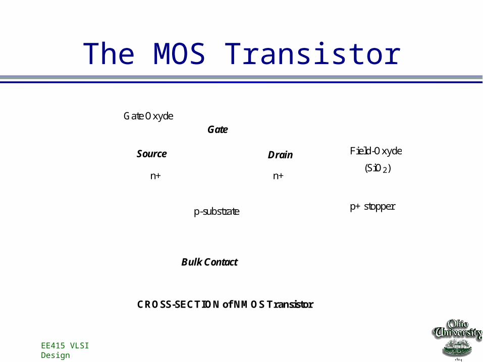
The MOS Transistor
n+n+
p-substrate
Field-Oxyde
(SiO2)
p+ stopper
Polysilicon
Gate Oxyde
DrainSource
Gate
Bulk Contact
CROSS-SECTION of NMOS Transistor
EE415 VLSI Design
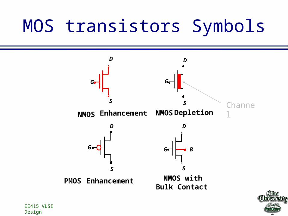
MOS transistors Symbols
D
S
G
D
S
G
G
S
D D
S
G
NMOS Enhancement NMOS
PMOS
Depletion
Enhancement
B
NMOS withBulk Contact
Channel
EE415 VLSI Design
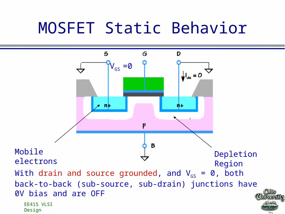
MOSFET Static Behavior
Depletion Region
VGS
=0
Mobile electrons
With drain and source grounded, and VGS = 0, both back-to-back (sub-source, sub-drain) junctions have 0V bias and are OFF
EE415 VLSI Design
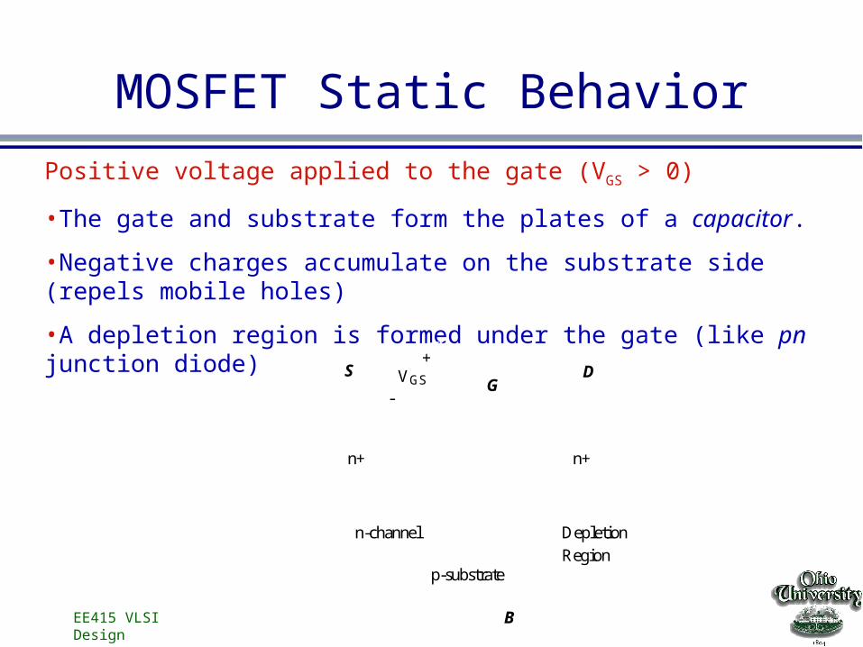
MOSFET Static Behavior
Positive voltage applied to the gate (VGS > 0)
•The gate and substrate form the plates of a capacitor.
•Negative charges accumulate on the substrate side (repels mobile holes)
•A depletion region is formed under the gate (like pn junction diode)
n+n+
p-substrate
DSG
B
VGS
+
-
Depletion
Region
n-channel
EE415 VLSI Design
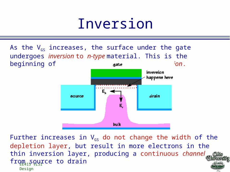
Inversion
As the VGS increases, the surface under the gate undergoes inversion to n-type material. This is the beginning of a phenomenon called strong inversion.
Further increases in VGS do not change the width of the depletion layer, but result in more electrons in the thin inversion layer, producing a continuous channel from source to drain
EE415 VLSI Design
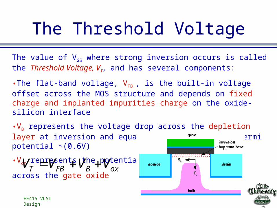
The Threshold Voltage
The value of VGS where strong inversion occurs is called the Threshold Voltage, VT , and has several components:
•The flat-band voltage, VFB , is the built-in voltage offset across the MOS structure and depends on fixed charge and implanted impurities charge on the oxide-silicon interface
•VB represents the voltage drop across the depletion layer at inversion and equals to minus twice the Fermi potential ~(0.6V)
•Vox represents the potential drop
across the gate oxide
oxBFBT VVVV
EE415 VLSI Design
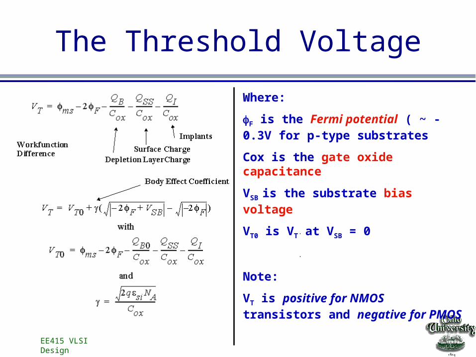
The Threshold Voltage
Where:
F is the Fermi potential ( ~ -0.3V for p-type substrates
Cox is the gate oxide capacitance
VSB is the substrate bias voltage
VT0 is VT at VSB = 0
Note:
VT is positive for NMOS transistors and negative for PMOS
EE415 VLSI Design
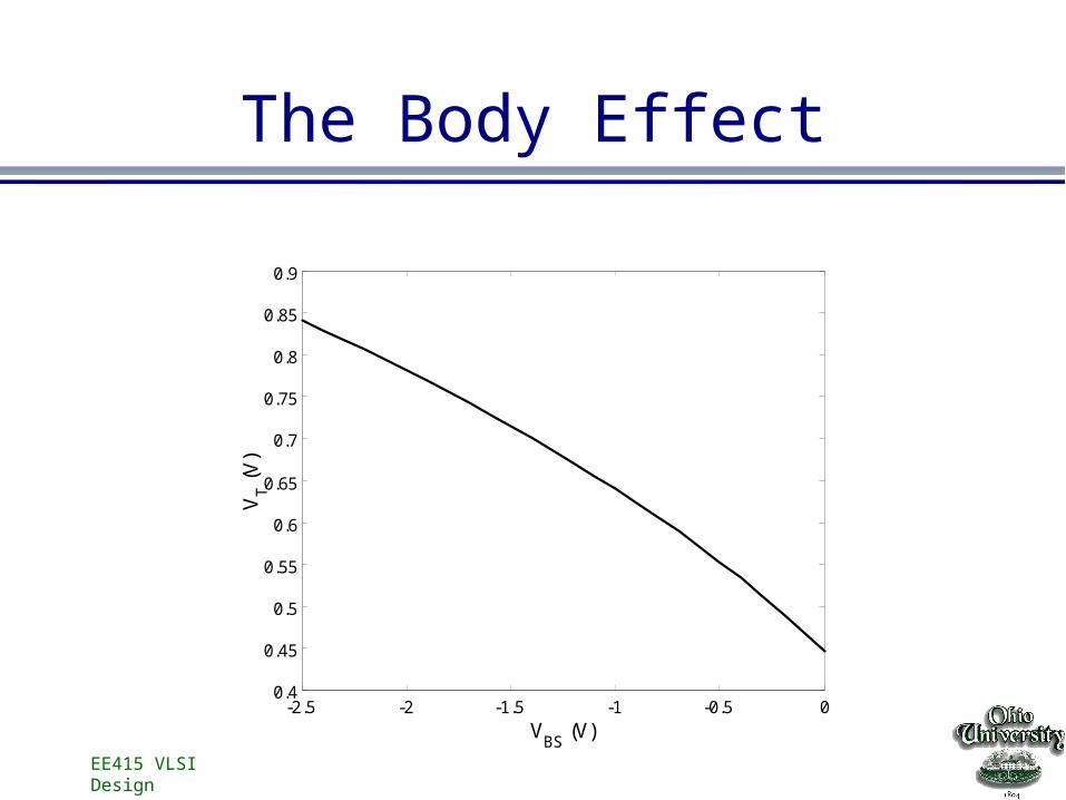
The Body Effect
-2.5 -2 -1.5 -1 -0.5 00.4
0.45
0.5
0.55
0.6
0.65
0.7
0.75
0.8
0.85
0.9
VBS
(V)
VT (
V)
EE415 VLSI Design
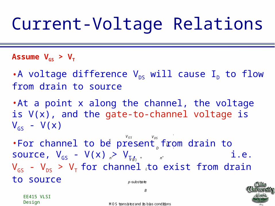
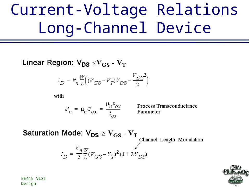
Current-Voltage Relations
n+n+
p-substrate
D
SG
B
VGS
xL
V(x) +–
VDS
ID
MOS transistor and its bias conditions
Assume VGS > VT
•A voltage difference VDS will cause ID to flow from drain to source
•At a point x along the channel, the voltage is V(x), and the gate-to-channel voltage is VGS - V(x)
•For channel to be present from drain to source, VGS - V(x) > VT, i.e. VGS - VDS > VT for channel to exist from drain to source
EE415 VLSI Design
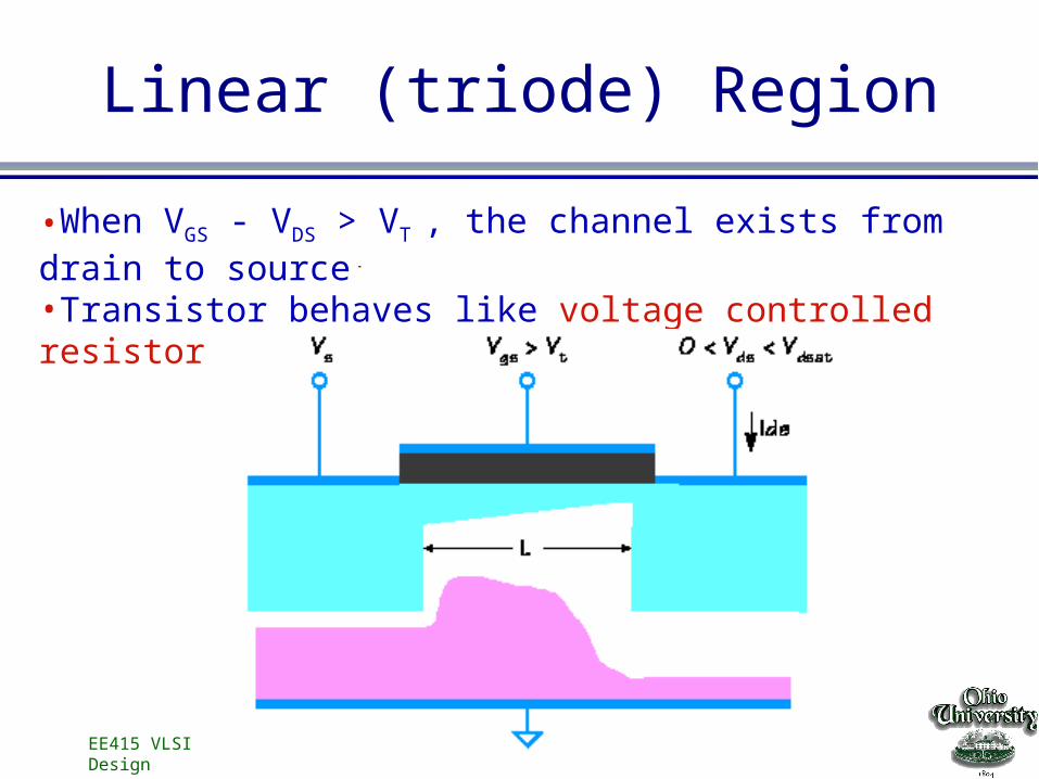
Linear (triode) Region
•When VGS - VDS > VT , the channel exists from drain to source•Transistor behaves like voltage controlled resistor
EE415 VLSI Design
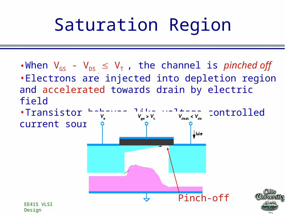
Saturation Region
•When VGS - VDS VT , the channel is pinched off•Electrons are injected into depletion region and accelerated towards drain by electric field•Transistor behaves like voltage-controlled current source
Pinch-off
EE415 VLSI Design
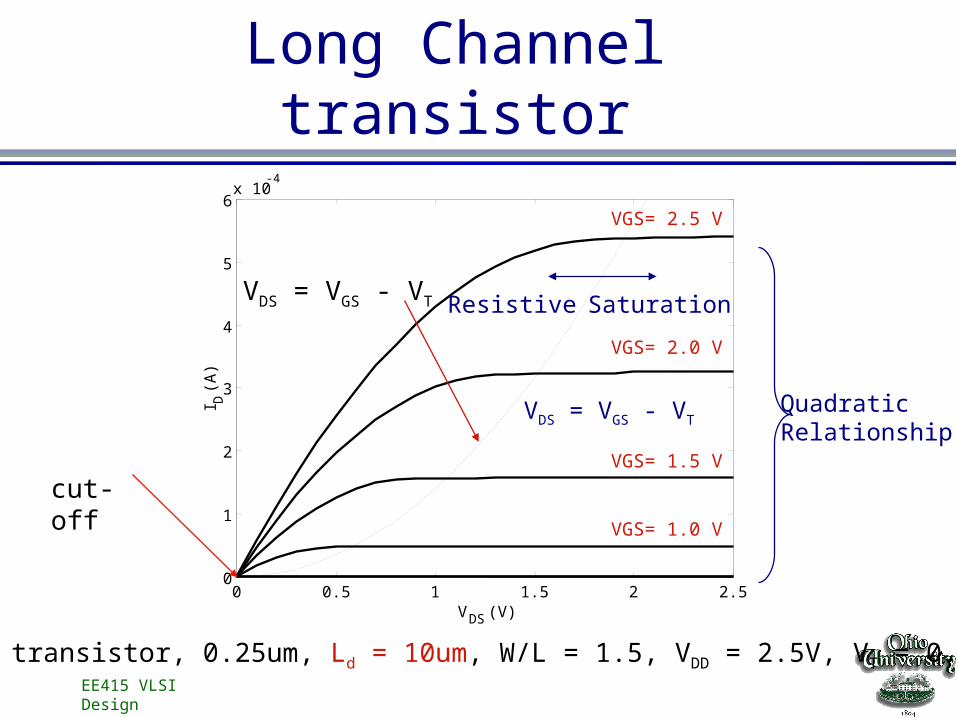
Current-Voltage RelationsLong-Channel Device
EE415 VLSI Design
Current-Voltage RelationsLong Channel transistor
NMOS transistor, 0.25um, Ld = 10um, W/L = 1.5, VDD = 2.5V, VT = 0.4V
QuadraticRelationship
0 0.5 1 1.5 2 2.50
1
2
3
4
5
6x 10
-4
VDS (V)
I D (
A)
VGS= 2.5 V
VGS= 2.0 V
VGS= 1.5 V
VGS= 1.0 V
Resistive Saturation
VDS = VGS - VT
VDS = VGS - VT
cut-off
EE415 VLSI Design
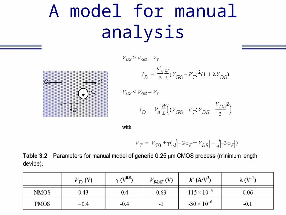
A model for manual analysis