Embed Size (px)
Citation preview

Charge-based MOS Transistor Modeling

Charge-based MOS Transistor
Modeling
The EKV model for low-powerand RF IC design
Christian C. EnzEric A. Vittoz
Copyright C© 2006 John Wiley & Sons Ltd, The Atrium, Southern Gate, Chichester,
West Sussex PO19 8SQ, England
Telephone (+44) 1243 779777
Email (for orders and customer service enquiries): [email protected]
Visit our Home Page on www.wiley.com
All Rights Reserved. No part of this publication may be reproduced, stored in a retrieval system
or transmitted in any form or by any means, electronic, mechanical, photocopying, recording,
scanning or otherwise, except under the terms of the Copyright, Designs and Patents Act 1988
or under the terms of a licence issued by the Copyright Licensing Agency Ltd, 90 Tottenham
Court Road, London W1T 4LP, UK, without the permission in writing of the Publisher.
Requests to the Publisher should be addressed to the Permissions Department, John Wiley &
Sons Ltd, The Atrium, Southern Gate, Chichester, West Sussex PO19 8SQ, England, or emailed
to [email protected], or faxed to (+44) 1243 770620.
Designations used by companies to distinguish their products are often claimed as trademarks. All brand
names and product names used in this book are trade names, service marks, trademarks or registered
trademarks of their respective owners. The Publisher is not associated with any product or vendor
mentioned in this book.
This publication is designed to provide accurate and authoritative information in regard to
the subject matter covered. It is sold on the understanding that the Publisher is not engaged
in rendering professional services. If professional advice or other expert assistance is
required, the services of a competent professional should be sought.
Other Wiley Editorial Offices
John Wiley & Sons Inc., 111 River Street, Hoboken, NJ 07030, USA
Jossey-Bass, 989 Market Street, San Francisco, CA 94103-1741, USA
Wiley-VCH Verlag GmbH, Boschstr. 12, D-69469 Weinheim, Germany
John Wiley & Sons Australia Ltd, 42 McDougall Street, Milton, Queensland 4064, Australia
John Wiley & Sons (Asia) Pte Ltd, 2 Clementi Loop #02-01, Jin Xing Distripark, Singapore 129809
John Wiley & Sons Canada Ltd, 22 Worcester Road, Etobicoke, Ontario, Canada M9W 1L1
Wiley also publishes its books in a variety of electronic formats. Some content that appears
in print may not be available in electronic books.
Library of Congress Cataloging-in-Publication Data
Enz, Christian.
Charge-based MOS transistor modelling : the EKV model for low-power and RF IC
design / Christian Enz and Eric Vittoz.
p. cm.
Includes bibliographical references and index.
ISBN-13: 978-0-470-85541-6 (alk. paper)
ISBN-10: 0-470-85541-X (alk. paper)
1. Metal oxide semiconductors–Mathematical models. 2. Metal oxide semiconductor
field-effect transistors–Mathematical models. I. Vittoz, Eric A., 1938– II. Title.
TK7871.99.M44E59 2006
621.3815′284–dc22 2006041744
A catalogue record for this book is available from the British Library
ISBN 13 978-0-470-85541-6
ISBN 10 0-470-85541-X
Typeset in 10/12pt Times by TechBooks, New Delhi, India
Printed and bound in Great Britain by Antony Rowe Ltd, Chippenham, Wiltshire
This book is printed on acid-free paper responsibly manufactured from sustainable forestry
in which at least two trees are planted for each one used for paper production.

To our families
Dominique, Adrien, Mathilde and Simon
and
Monique, Nathalie and Didier

Contents
Foreword xiii
Preface xv
List of Symbols xvii
1 Introduction 11.1 The Importance of Device Modeling for IC Design 1
1.2 A Short History of the EKV MOS Transistor Model 2
1.3 The Book Structure 5
Part I The Basic Long-Channel Intrinsic Charge-Based Model 7
2 Definitions 92.1 The N-channel Transistor Structure 9
2.2 Definition of Charges, Current, Potential, and Electric Fields 10
2.3 Transistor Symbol and P-channel Transistor 11
3 The Basic Charge Model 133.1 Poisson’s Equation and Gradual Channel Approximation 13
3.2 Surface Potential as a Function of Gate Voltage 17
3.3 Gate Capacitance 18
3.4 Charge Sheet Approximation 20
3.5 Density of Mobile Inverted Charge 21
3.5.1 Mobile Charge as a Function of Gate Voltage and Surface Potential 21
3.5.2 Mobile Charge as a Function of Channel Voltage and
Surface Potential 23
3.6 Charge-Potential Linearization 23
3.6.1 Linearization of Qi(Ψs) 23
3.6.2 Linearized Bulk Depletion Charge Qb 26
3.6.3 Strong Inversion Approximation 27
3.6.4 Evaluation of the Slope Factor 29
3.6.5 Compact Model Parameters 32
viii CONTENTS
4 Static Drain Current 334.1 Drain Current Expression 33
4.2 Forward and Reverse Current Components 35
4.3 Modes of Operation 36
4.4 Model of Drain Current Based on Charge Linearization 37
4.4.1 Expression Valid for All Levels of Inversion 37
4.4.2 Compact Model Parameters 39
4.4.3 Inversion Coefficient 40
4.4.4 Approximation of the Drain Current in Strong Inversion 41
4.4.5 Approximation of the Drain Current in Weak Inversion 43
4.4.6 Alternative Continuous Models 45
4.5 Fundamental Property: Validity and Application 46
4.5.1 Generalization of Drain Current Expression 46
4.5.2 Domain of Validity 46
4.5.3 Causes of Degradation 48
4.5.4 Concept of Pseudo-Resistor 49
4.6 Channel Length Modulation 50
4.6.1 Effective Channel Length 50
4.6.2 Weak Inversion 52
4.6.3 Strong Inversion 52
4.6.4 Geometrical Effects 53
5 The Small-Signal Model 555.1 The Static Small-Signal Model 55
5.1.1 Transconductances 55
5.1.2 Residual Output Conductance in Saturation 60
5.1.3 Equivalent Circuit 61
5.1.4 The Normalized Transconductance to Drain Current Ratio 62
5.2 A General NQS Small-Signal Model 65
5.3 The QS Dynamic Small-Signal Model 72
5.3.1 Intrinsic Capacitances 72
5.3.2 Transcapacitances 74
5.3.3 Complete QS Circuit 75
5.3.4 Domains of Validity of the Different Models 77
6 The Noise Model 816.1 Noise Calculation Methods 81
6.1.1 General Expression 81
6.1.2 Long-Channel Simplification 86
6.2 Low-Frequency Channel Thermal Noise 87
6.2.1 Drain Current Thermal Noise PSD 87
6.2.2 Thermal Noise Excess Factor Definitions 89
6.2.3 Circuit Examples 91
6.3 Flicker Noise 96
6.3.1 Carrier Number Fluctuations (Mc Worther Model) 96
6.3.2 Mobility Fluctuations (Hooge Model) 101
6.3.3 Additional Contributions Due to the Source and
Drain Access Resistances 103
CONTENTS ix
6.3.4 Total 1/f Noise at the Drain 104
6.3.5 Scaling Properties 105
6.4 Appendices 106
Appendix: The Nyquist and Bode Theorems 106
Appendix: General Noise Expression 108
7 Temperature Effects and Matching 1117.1 Introduction 111
7.2 Temperature Effects 112
7.2.1 Variation of Basic Physical Parameters 112
7.2.2 Variation of the Voltage–Charge Characteristics 116
7.2.3 Variation of the Voltage–Current Characteristics 118
7.2.4 Variation of the Current–Charge Characteristics 120
7.3 Matching 120
7.3.1 Introduction 120
7.3.2 Deterministic Mismatch 121
7.3.3 Random Mismatch 125
Part II The Extended Charge-Based Model 131
8 Nonideal Effects Related to the Vertical Dimension 1338.1 Introduction 133
8.2 Mobility Reduction Due to the Vertical Field 133
8.3 Nonuniform Vertical Doping 138
8.3.1 Introduction and General Case 138
8.3.2 Constant Gradient Doping Profile 139
8.3.3 Step Profile 141
8.3.4 Effect on the Basic Model 147
8.4 Polysilicon Depletion 148
8.4.1 Definition of the Effect 148
8.4.2 Effect on the Mobile Inverted Charge 149
8.4.3 Slope Factors and Pinch-Off Surface Potential 150
8.4.4 Voltage Slope Factor nv 152
8.4.5 Charge Slope Factor nq 153
8.4.6 Effect on Qi(V ), Currents, and Transconductances 154
8.4.7 Strong Inversion Approximation 155
8.5 Band Gap Widening 156
8.5.1 Introduction 156
8.5.2 Extension of the General Charge–Voltage Expression 158
8.5.3 Extension of the General Current–Voltage Expression 160
8.6 Gate Leakage Current 161
9 Short-Channel Effects 1679.1 Velocity Saturation 167
9.1.1 Velocity-Field Models 169
9.1.2 Effect of VS on the Drain Current 171
9.1.3 Effect of VS on the Transconductances 181
x CONTENTS
9.2 Channel Length Modulation 186
9.3 Drain Induced Barrier Lowering 189
9.3.1 Introduction 189
9.3.2 Evaluation of the Surface Potential 189
9.3.3 Effect on the Drain Current 194
9.3.4 Effect on Small-Signal Parameters in Weak Inversion 196
9.4 Short-Channel Thermal Noise Model 197
9.4.1 Thermal Noise Drain Conductance 198
9.4.2 Effect of VS and Carrier Heating on Thermal Noise 205
9.4.3 Effects of Vertical Field Mobility Reduction and Channel
Length Modulation 209
9.4.4 Summary 211
10 The Extrinsic Model 21310.1 Extrinsic Part of the Device 213
10.2 Access Resistances 215
10.2.1 Source and Drain Resistances 215
10.2.2 The Gate Resistance 217
10.3 Overlap Regions 220
10.3.1 Overlap Capacitances 220
10.3.2 Overlap Gate Leakage Current 223
10.4 Source and Drain Junctions 223
10.4.1 Source and Drain Diodes Large-Signal Model 223
10.4.2 Source and Drain Junction Capacitances 224
10.4.3 Source and Drain Junction Conductances 226
10.5 Extrinsic Noise Sources 226
Part III The High-Frequency Model 229
11 Equivalent Circuit at RF 23111.1 RF MOS Transistor Structure and Layout 231
11.2 What Changes at RF? 231
11.3 Transistor Figures of Merit 232
11.3.1 Transit Frequency 232
11.3.2 Maximum Frequency of Oscillation fmax 236
11.3.3 Minimum Noise Figure 238
11.3.4 Moderate and Weak Inversion for RF Circuits 239
11.4 Equivalent Circuit at RF 240
11.4.1 Equivalent Circuit at RF 240
11.4.2 Intradevice Substrate Coupling and Substrate Resistive
Networks 242
11.4.3 Practical Implementation Issues 247
12 The Small-Signal Model at RF 24912.1 The Equivalent Small-Signal Circuit at RF 249
12.2 Y-Parameters Analysis 251
12.3 The Large-Signal Model at RF 257
CONTENTS xi
13 The Noise Model at RF 26113.1 The HF Noise Parameters 261
13.1.1 The Noisy Two-Port 261
13.1.2 The Correlation Admittance 263
13.1.3 The Noise Factor 265
13.1.4 Minimum Noise Factor 266
13.2 The High-Frequency Thermal Noise Model 267
13.2.1 Generalized High-Frequency Noise Model 268
13.2.2 The Two-Transistor Approach at High Frequency 269
13.2.3 Generic PSDs Derivation 272
13.2.4 First-Order Approximation 273
13.2.5 Higher Order Effects 279
13.3 HF Noise Parameters of a Common-Source Amplifier 282
13.3.1 Simple Equivalent Circuit Including Induced Gate Noise and
Drain Noise 282
13.3.2 Equivalent Circuit Including Induced Gate Noise, Drain Noise,
Gate and Substrate Resistances Noise 288
References 291
Index 299

Foreword
Modern electronic technology is largely based on MOS integrated circuits containing both
analog and digital parts. In designing such circuits with high performance, a correct MOS
transistor model is a must. The designer needs a model he or she can rely on, which correctly
describes the numerous physical phenomena in MOS transistors, allowing the performance of
a circuit composed of such devices to be predicted with accuracy during circuit simulation. In
addition, for preliminary “hand” analysis and design, it is desirable to have a simple model
that makes evident the inter-relations between the various parameters, and allows the designer
to correctly identify the trade-offs involved. The EKV approach to MOS transistor modeling
combines both of these attributes.
The EKV model is the result of a large body of work by Drs C. C. Enz, F. Krummenacher,
and E. A. Vittoz, and several of their students and colleagues. The work has its origins in the
pioneering work at CEH (now CSEM), on micropower devices and circuits for watches in the
late sixties. This has given the EKV model development a unique aspect: it originated with
highly competent circuit designers, notably analog ones, and was developed by them, or at
least with constant feedback from them, every step of the way. Thus, it not only describes
the physics of the MOS transistor, but takes into account carefully what circuit designers
need. The result is a model that is accurate and predictive, correctly treats the MOSFET as a
four-terminal, nominally symmetric device, has smooth behavior without discontinuities in all
regions of operation, and correctly predicts small-signal parameters. In addition, the basic part
of the model consists of a simple set of equations that are intuitively appealing, which makes
it possible for the circuit designer to have a feel for the model and its parameters, rather than
treating the model simply as a black box in which no designer dares to tread. This helps make
circuit design a systematic process, and less a cut-and-try approach.
Drs. Enz and Vittoz, well-known for their contributions to MOS devices and circuits, have
done a great job putting together a streamlined presentation of the EKV model. The book
covers every aspect of the model, from DC large-signal I-V equations, to charge modeling,
nonquasi-static effects, small-signal modeling, noise, small-channel effects, and matching. I
have followed the work of the authors and their colleagues for many years with appreciation,
and I am delighted to see their results presented in this unified manner. This book will help
spread the understanding and use of the EKV model, as the latter certainly deserves.
Prof. Y. Tsividis
Columbia University, New-York

Preface
The aggressive downscaling of CMOS technologies that has been going on for more than
25 years has led to an increase in the number of transistors per chip and hence extend the
functionality while at the same time dramatically pushing the speed performance. Although
these tremendous speed improvements have been mainly driven by the requirements of VLSI
digital chips, they have also been exploited for analog and RF circuits. Today, ultra deep-
submicron (UDSM) technologies have caught up and even surpassed the transit frequencies
achieved by bipolar transistors. This has clearly opened the door to full CMOS highly integrated
solutions for wireless applications. Of course, in addition to high transit frequency, good noise
performance and low-power consumption are required as well. Since the noise figure also
decreases as the transit frequency is increased, it has also clearly taken advantage of the
downscaling of the transistor length. At the same time, the supply voltage has had to be
decreased progressively in order to limit high electric fields within the device and hence avoid
the related high-field effects. The threshold voltage could unfortunately not be scaled in the
same proportion without strongly increasing the drain leakage current, which is now seriously
affecting the static power consumption of digital chips. This has resulted in a decrease of the
overdrive voltage which in turn has moved the operating points of analog transistors more
and more from strong inversion to moderate inversion and even into weak inversion. From
this perspective, it is important to have a model that accurately predicts the behavior of the
MOS transistor in all regions of operation, from weak to strong inversion, through moderate
inversion, in a consistent way. This was the primary motivation for developing what today is
known as the EKV model.
The purpose of this book is to assemble and explain in a coherent manner all the know-how
and all the publications related to the particular MOS transistor modeling approach embodied
by the EKV model. This model borrows from the work of a long line of researchers, starting
in the early times of semiconductor physics. It has its roots in the search of early designers of
very low-power and low-voltage integrated circuits for a description of the transistor behavior
fulfilling their specific needs. This book focuses on this particular line of research, with no
intention to present all alternative ways of modeling the transistor. Being written by analog
circuit designers, it is clearly design-oriented with the purpose of describing the transistor as
the basic component of integrated circuits, rather than the result of a sequence of physical
processing steps. It gives to emphasis highlighting the properties of the device that can be used
by designers to build new robust circuits, or to understand existing circuits and assess their
robustness. The book is organized in three hierarchically structured parts. It firstly describes
xvi PREFACE
the basic behavior of the generic MOS transistor, then focuses on additional effects essentially
due to scaling down the device dimensions, and finally discusses the transistors to be used in
RF circuits.
Based on the charge in the channel, the EKV model describes in a continuous manner the
static, dynamic and noise characteristics of the transistor down to very low current levels. The
basic model requires a very limited set of parameters, all of them directly related to basic
independent physical parameters. Intended for analog designers, it conserves the intrinsic
source-drain symmetry of the transistor by using the substrate as the voltage reference and
by introducing the concept of forward and reverse components of the drain current. This
symmetrical approach makes it easier to understand the various modes of static operation
of the device, and to describe them by a single uncomplicated equation. The charge-based
approach lends itself naturally to a coherent description of the dynamic and noise behavior of
the transistor.
The authors want to acknowledge the numerous persons who contributed directly and
indirectly to this book. We are grateful to Dr Francois Krummenacher for his invaluable
contribution to the EKV model and for his many inputs and suggestions that greatly helped
us to write this book. We have benefited from the many discussions we had with Jean-Michel
Sallese and Ananda Roy who helped us to clarify many fine points along the process of writing
this book. We also would like to acknowledge the contribution of all the other members of the
EKV development team, who each brought their own contribution to the EKV model: Matthias
Bucher, Christophe Lallement, Alain-Serge Porret, Wladek Grabinski. Our gratitude also goes
to Henri Oguey and Stephan Cserveny who pioneered the work for a continuous model and
paved the way for the current EKV model.
Finally, we would like to give special thanks to our families – Dominique, Adrien, Mathilde
and Simon Enz, and Monique, Nathalie and Didier Vittoz – for their support and understanding
during this seemingly endless task.
Christian C. Enz, Eric A. Vittoz
St-Aubin-Sauges, Switzerland
Cernier, Switzerland
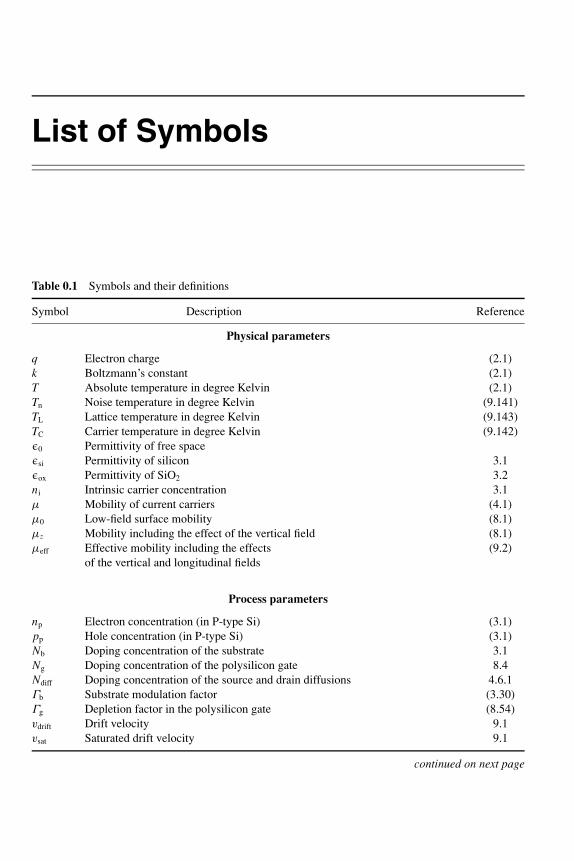
List of Symbols
Table 0.1 Symbols and their definitions
Symbol Description Reference
Physical parameters
q Electron charge (2.1)
k Boltzmann’s constant (2.1)
T Absolute temperature in degree Kelvin (2.1)
Tn Noise temperature in degree Kelvin (9.141)
TL Lattice temperature in degree Kelvin (9.143)
TC Carrier temperature in degree Kelvin (9.142)
ǫ0 Permittivity of free space
ǫsi Permittivity of silicon 3.1
ǫox Permittivity of SiO2 3.2
ni Intrinsic carrier concentration 3.1
µ Mobility of current carriers (4.1)
µ0 Low-field surface mobility (8.1)
µz Mobility including the effect of the vertical field (8.1)
µeff Effective mobility including the effects (9.2)
of the vertical and longitudinal fields
Process parameters
np Electron concentration (in P-type Si) (3.1)
pp Hole concentration (in P-type Si) (3.1)
Nb Doping concentration of the substrate 3.1
Ng Doping concentration of the polysilicon gate 8.4
Ndiff Doping concentration of the source and drain diffusions 4.6.1
Γb Substrate modulation factor (3.30)
Γg Depletion factor in the polysilicon gate (8.54)
vdrift Drift velocity 9.1
vsat Saturated drift velocity 9.1
continued on next page
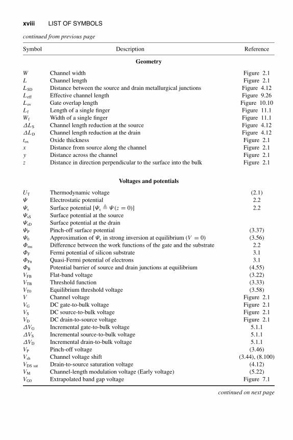
xviii LIST OF SYMBOLS
continued from previous page
Symbol Description Reference
Geometry
W Channel width Figure 2.1
L Channel length Figure 2.1
LSD Distance between the source and drain metallurgical junctions Figure 4.12
Leff Effective channel length Figure 9.26
Lov Gate overlap length Figure 10.10
L f Length of a single finger Figure 11.1
Wf Width of a single finger Figure 11.1
∆LS Channel length reduction at the source Figure 4.12
∆LD Channel length reduction at the drain Figure 4.12
tox Oxide thickness Figure 2.1
x Distance from source along the channel Figure 2.1
y Distance across the channel Figure 2.1
z Distance in direction perpendicular to the surface into the bulk Figure 2.1
Voltages and potentials
UT Thermodynamic voltage (2.1)
Ψ Electrostatic potential 2.2
Ψs Surface potential [Ψs Ψ (z = 0)] 2.2
ΨsS Surface potential at the source
ΨsD Surface potential at the drain
ΨP Pinch-off surface potential (3.37)
Ψ0 Approximation of Ψs in strong inversion at equilibrium (V = 0) (3.56)
Φms Difference between the work functions of the gate and the substrate 2.2
ΦF Fermi potential of silicon substrate 3.1
ΦFn Quasi-Fermi potential of electrons 3.1
ΦB Potential barrier of source and drain junctions at equilibrium (4.55)
VFB Flat-band voltage (3.22)
VTB Threshold function (3.33)
VT0 Equilibrium threshold voltage (3.58)
V Channel voltage Figure 2.1
VG DC gate-to-bulk voltage Figure 2.1
VS DC source-to-bulk voltage Figure 2.1
VD DC drain-to-source voltage Figure 2.1
∆VG Incremental gate-to-bulk voltage 5.1.1
∆VS Incremental source-to-bulk voltage 5.1.1
∆VD Incremental drain-to-bulk voltage 5.1.1
VP Pinch-off voltage (3.46)
Vsh Channel voltage shift (3.44), (8.100)
VDS sat Drain-to-source saturation voltage (4.12)
VM Channel-length modulation voltage (Early voltage) (5.22)
VG0 Extrapolated band gap voltage Figure 7.1
continued on next page
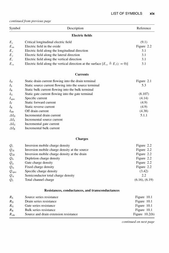
LIST OF SYMBOLS xix
continued from previous page
Symbol Description Reference
Electric fields
Ec Critical longitudinal electric field (9.1)
Eox Electric field in the oxide Figure 2.2
Ex Electric field along the longitudinal direction 3.1
Ey Electric field along the lateral direction 3.1
Ez Electric field along the vertical direction 3.1
Ezs Electric field along the vertical direction at the surface [Ezs Ez(z = 0)] 3.1
Currents
ID Static drain current flowing into the drain terminal Figure 2.1
IS Static source current flowing into the source terminal 5.3
IB Static bulk current flowing into the bulk terminal
IG Static gate current flowing into the gate terminal (8.107)
Ispec Specific current (4.14)
IF Static forward current (4.9)
IR Static reverse current (4.9)
ID0 Off drain current (4.38)
∆ID Incremental drain current 5.1.1
∆IS Incremental source current
∆IG Incremental gate current
∆IB Incremental bulk current
Charges
Qi Inversion mobile charge density Figure 2.2
QiS Inversion mobile charge density at the source Figure 2.2
QiD Inversion mobile charge density at the drain Figure 2.2
Qb Depletion charge density Figure 2.2
Qg Gate charge density Figure 2.2
Qfc Fixed charge density Figure 2.2
Qspec Specific charge density (3.42)
Qsi Semiconductor total charge density 2.2
QI Total channel charge (6.16), (6.19)
Resistances, conductances, and transconductances
RS Source series resistance Figure 10.1
RD Drain series resistance Figure 10.1
RG Gate series resistance Figure 10.1
RB Bulk series resistance Figure 10.1
Rsde Source and drain extension resistance Figure 10.2(b)
continued on next page
xx LIST OF SYMBOLS
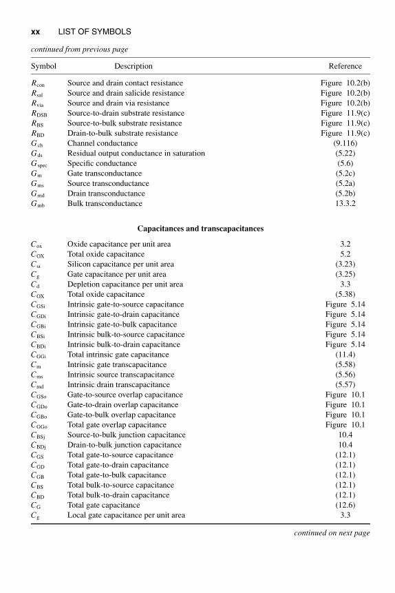
continued from previous page
Symbol Description Reference
Rcon Source and drain contact resistance Figure 10.2(b)
Rsal Source and drain salicide resistance Figure 10.2(b)
Rvia Source and drain via resistance Figure 10.2(b)
RDSB Source-to-drain substrate resistance Figure 11.9(c)
RBS Source-to-bulk substrate resistance Figure 11.9(c)
RBD Drain-to-bulk substrate resistance Figure 11.9(c)
Gch Channel conductance (9.116)
Gds Residual output conductance in saturation (5.22)
Gspec Specific conductance (5.6)
Gm Gate transconductance (5.2c)
Gms Source transconductance (5.2a)
Gmd Drain transconductance (5.2b)
Gmb Bulk transconductance 13.3.2
Capacitances and transcapacitances
Cox Oxide capacitance per unit area 3.2
COX Total oxide capacitance 5.2
Csi Silicon capacitance per unit area (3.23)
Cg Gate capacitance per unit area (3.25)
Cd Depletion capacitance per unit area 3.3
COX Total oxide capacitance (5.38)
CGSi Intrinsic gate-to-source capacitance Figure 5.14
CGDi Intrinsic gate-to-drain capacitance Figure 5.14
CGBi Intrinsic gate-to-bulk capacitance Figure 5.14
CBSi Intrinsic bulk-to-source capacitance Figure 5.14
CBDi Intrinsic bulk-to-drain capacitance Figure 5.14
CGGi Total intrinsic gate capacitance (11.4)
Cm Intrinsic gate transcapacitance (5.58)
Cms Intrinsic source transcapacitance (5.56)
Cmd Intrinsic drain transcapacitance (5.57)
CGSo Gate-to-source overlap capacitance Figure 10.1
CGDo Gate-to-drain overlap capacitance Figure 10.1
CGBo Gate-to-bulk overlap capacitance Figure 10.1
CGGo Total gate overlap capacitance Figure 10.1
CBSj Source-to-bulk junction capacitance 10.4
CBDj Drain-to-bulk junction capacitance 10.4
CGS Total gate-to-source capacitance (12.1)
CGD Total gate-to-drain capacitance (12.1)
CGB Total gate-to-bulk capacitance (12.1)
CBS Total bulk-to-source capacitance (12.1)
CBD Total bulk-to-drain capacitance (12.1)
CG Total gate capacitance (12.6)
Cg Local gate capacitance per unit area 3.3
continued on next page
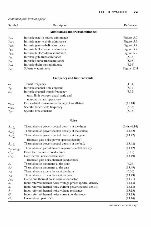
LIST OF SYMBOLS xxi
continued from previous page
Symbol Description Reference
Admittances and transadmittances
YGSi Intrinsic gate-to-source admittance Figure 5.9
YGDi Intrinsic gate-to-drain admittance Figure 5.9
YGBi Intrinsic gate-to-bulk admittance Figure 5.9
YBSi Intrinsic bulk-to-source admittance Figure 5.9
YBDi Intrinsic bulk-to-drain admittance Figure 5.9
Ym Intrinsic gate transadmittance (5.36)
Yms Intrinsic source transadmittance (5.36)
Ymd Intrinsic drain transadmittance (5.36)
Ysub Substrate admittance Figure 12.4
Frequency and time constants
ωt Transit frequency (11.4)
τqs Intrinsic channel time constant (5.32)
ωqs Intrinsic channel transit frequency (5.32)
(also limit between quasi-static and
non-quasi static operation)
ωmax Extrapolated maximum frequency of oscillation (11.18)
ωspec Specific (or critical) frequency (5.33)
τspec Specific time constant (5.33)
Noise
S∆I 2nD
Thermal noise power spectral density at the drain (6.4), (6.14)
S∆I 2nS
Thermal noise power spectral density at the source (13.42)
S∆I 2nG
Thermal noise power spectral density at the gate (13.42)
(induced gate noise power spectral density)
S∆I 2nB
Thermal noise power spectral density at the bulk (13.42)
S∆InG∆I ∗nD
Thermal noise gate-drain cross-power spectral density (13.42)
GnD Drain thermal noise conductance (6.15)
GnG Gate thermal noise conductance (13.49)
(induced gate noise thermal conductance)
δnD Thermal noise parameter at the drain (6.26)
δnG Thermal noise parameter at the gate (13.49)
γnD Thermal noise excess factor at the drain (6.30)
γnG Thermal noise excess factor at the gate (13.49)
ρGD Gate-drain thermal noise correlation factor (13.71)
Sv Input-referred thermal noise voltage power spectral density (13.13)
Si Input-referred thermal noise current power spectral density (13.13)
Rv Input-referred thermal noise voltage resistance (13.13)
G i Input-referred thermal noise current conductance (13.13)
G iu Uncorrelated part of G i (13.14)
continued on next page
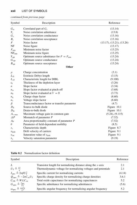
xxii LIST OF SYMBOLS
continued from previous page
Symbol Description Reference
G ic Correlated part of G i (13.14)
Yc Noise correlation admittance (13.8)
Gc Noise correlation conductance (13.16)
Bc Noise correlation susceptance (13.16)
F Noise factor (13.17), (13.21), (13.26)
NF Noise figure (13.17)
Fmin Minimum noise factor (13.25)
NFmin Minimum noise figure (13.25)
Yopt Optimum source admittance for F = Fmin (13.24)
Gopt Optimum source conductance (13.24)
Bopt Optimum source susceptance (13.24)
Other
ρ Charge concentration (3.1)
LD Extrinsic Debye length (3.15)
Lc0 Characteristic length for DIBL (9.100)
td Thickness of the depletion layer (3.26)
n Slope factor (3.34)
nw Slope factor evaluated at pinch-off (3.68)
n0 Slope factor evaluated at V = 0 (3.73)
nq Charge slope factor (8.60)
nv Voltage slope factor (8.60)
β Transconductance factor or transfer parameter (4.7)
DS Source-to-bulk diode Figure 10.1
DD Drain-to-bulk diode Figure 10.1
Av max Maximum voltage gain in common gate (5.24), (9.115)
∆P Mismatch of parameter P (7.52)
AP Area proportionality constant of parameter P (7.52)
θ Parameter of field-dependent mobility (8.5)
zc Characteristic depth Figure 8.7
vdrift Drift velocity of carriers Figure 9.1
vsat Saturation value of vdrift Figure 9.1
λc Velocity saturation parameter (9.19)
Table 0.2 Normalization factor definition
Symbol Description Reference
L Transistor length for normalizing distance along the x-axis 2.1
UT kTq
Thermodynamic voltage for normalizing voltages and potentials 2.1
Ispec 2nβU 2T Specific current for normalizing currents (4.14)
Qspec −2nCoxUT Specific charge density for normalizing charge densities 3.6.1
COX W LCox Total oxide capacitance for normalizing capacitances 5.2
Gspec Ispec
UTSpecific admittance for normalizing admittances (5.6)
ωspec µnUT
L2 Specific angular frequency for normalizing angular frequency 5.2
LIST OF SYMBOLS xxiii
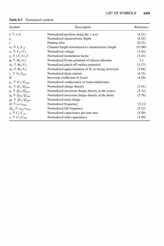
Table 0.3 Normalized symbols
Symbol Description Reference
ξ x/L Normalized position along the x-axis (4.21)
ζc Normalized characteristic depth (8.24)
ν Doping ratio (8.32)
λ0 L/Lc0 Channel length normalized to characteristic length (9.100)
vx VX/UT Normalized voltage (3.43)
γj (Γj/UT)2 Normalized modulation factor (3.43)
φf ΦF/UT Normalized Fermi potential of silicon substrate 3.1
ψp ΨP/UT Normalized pinch-off surface potential (3.37)
ψ0 Ψ0/UT Normalized approximation of Ψs in strong inversion (3.66)
ix IX/Ispec Normalized drain current (4.15)
IC Inversion coefficient or factor (4.26)
gx Gx/Gspec Normalized conductance or transconductance
qx Qx/Qspec Normalized charge density (3.41)
qs QiS/Qspec Normalized inversion charge density at the source (5.7a)
qd QiD/Qspec Normalized inversion charge density at the drain (5.7b)
qX Q X/Qspec Normalized total charge
Ω ω/ωspec Normalized frequency 13.2.2
Ωqs ωqs/ωspec Normalized QS frequency (5.32)
cj Cj/Cox Normalized capacitance per unit area (5.50)
cJ CJ/COX Normalized total capacitance (5.50)


1 Introduction
This chapter explains the basic motivations for developing MOS transistor models that can be
used for the design of complementary MOS (CMOS) integrated circuits. It then gives a short
history of the EKV MOS transistor model starting from the early development, motivated by
the design of micropower circuits for watch applications, to the most recent developments.
Finally, the structure of the book is highlighted in order to help the reader organizing his
reading.
1.1 THE IMPORTANCE OF DEVICE MODELINGFOR IC DESIGN
Modern large-scale integrated circuits are essentially composed of MOS transistors and their
interconnections. Therefore, the design of such circuits requires some kind of a model for the
transistors.
For noncritical digital circuits, this model may in principle be very simple. Indeed, modeling
each transistor as an on–off switch would be sufficient to design purely logic circuits. However,
as soon as there are critical races among transitions, the model must be extended to describe the
dynamic behavior of the device, in order to obtain the rise and fall time of these transitions. This
dynamic behavior is also needed when the frequency of operation approaches its maximum
limit. With the reduction of supply voltage, more details must be introduced, such as the
residual current of blocked transistors, the importance of which is increased.
Analog circuits contain usually a smaller number of transistors, but they are even more
dependent on the exact behavior of each transistor. The design of high-performance analog
circuits therefore requires a very detailed model of the transistor. This model must include a
precise description of the voltage–current relationships, including the effect of the source that
is often not grounded, and of the dynamic behavior of the device. Its behavior with respect to
noise and to temperature variations must also be accounted for.
A transistor model intended for circuit design should serve two essential purposes:
It should first provide a good understanding of the various properties of the device to facilitate
the synthesis of optimum circuit architectures. Indeed, in order to build robust circuits, the
Charge-Based MOS Transistor Modeling: The EKV Model for Low-Power and RF IC Design C. Enz and E. VittozC© 2006 John Wiley & Sons, Ltd.
2 INTRODUCTION
physical properties of the transistor must be exploited in a way that is minimally dependent on
temperature and process variations. For this purpose, the model should be explicit. It should
“speak to the mind,” using no complicated or chained equations. Clarity should supersede
precision and can be enhanced by means of graphical representations. This important aspect
of a model is often underestimated and overlooked. It will be emphasized in this book, in
particular in Part I, which essentially describes what can be called the core of the model.
Second, the model should be adapted to numerical simulations on a computer, embedded
in a circuit simulator. For this purpose, precision supersedes clarity, and second-order effects
must be accounted for. This can be obtained by predistorting variables, by chaining equations
and/or by providing additional layers around a core model. The model does not need to be fully
explicit, but it should be compact: it should use sufficiently simple expressions with minimum
need for numerical iterations, in order to limit the computation time.
A transistor model should include a minimum number of process-dependent device param-
eters. This is to facilitate the very heavy task of extracting and following-up the value of these
parameters, with their statistical distribution and temperature dependency.
Now, the correlation between these parameters (with process and temperature variations)
must be known, in order to avoid designing circuits for irrelevant worst cases. For this reason,
the device parameters should be explicitly based on independent and measurable process pa-
rameters. This is essential to be able to ascertain their amount of correlations while avoiding
the almost impossible task of measuring all these correlations. It also makes the model predic-
tive, allowing to foresee the characteristics of the transistor and hence the performance of the
resulting circuits even before measuring the device.
The EKV model described in this book is believed to meet all the above expectations. It
serves the two main purposes in a coherent manner. Its core requires just a few parameters
to describe all the basic properties of the long-channel intrinsic device in an explicit manner.
Layers are added to this core to account for short-channel and secondary effects.
1.2 A SHORT HISTORY OF THE EKV MOSTRANSISTOR MODEL
The model presented in this book results from a series of direct and indirect contributions along
several decades. Its origins can be traced back to the early developments of electronic watches
at CEH (French acronym for Watchmakers Electronic Center) in Switzerland [2].
The total power consumption had to be extremely low, less than 1μW, to ensure a few
years of life to the single button-size cell battery. After the very first versions based on bipolar
transistors [3], the CMOS technology was soon identified as the best approach to implement the
digital electronic circuitry needed in a watch using a crystal resonator as the time reference.
Supply voltage had to be very low, compatible with the 1.3 V delivered by the cell, so the
development of low-threshold CMOS was a major challenge in the late 1960’s [4].
The digital circuitry was essentially an asynchronous chain of divide-by-two stages. The
main design problem was to minimize the number of node transitions in order to minimize the
dynamic power. Another one was the elimination of logic hazards to improve the robustness
against large local variations of the small gate voltage overhead, and this led to the first single
clock circuits [5–7]. For these digital circuits, MOS transistors could be considered just as
switches and hence no special model was required.
A SHORT HISTORY OF THE EKV MOS TRANSISTOR MODEL 3
The problem was very different for the few analog subcircuits. Most important was the
circuitry needed to sustain the oscillation of the quartz crystal resonator (the quartz oscillator).
Each transistor had to be biased at a drain current much below 1μA. Early measurements
carried out in 1967 showed that the transistor behaved in a very strange manner at these very
low current levels. Indeed, the well-known square-law transfer characteristics were replaced
by an exponential over more than 5 order of magnitude of the drain current, very similar to
bipolar transistors. This is how weak inversion popped out to the attention of micropower
circuit designers in the late 1960s.
At that time, no transistor model was available for weak inversion, but they started coming
out in subsequent years, mainly to account for what appears in digital circuits as a leakage
current of blocked transistors. In 1972, M. B. Barron published a model for the grounded source
device showing the exponential dependencies on drain voltage and on surface potential, with a
rather complex expression relating the surface potential to the gate voltage [8]. The same year,
R. M. Swanson and J. D. Meindl [9] showed that this relation could be accounted for by means
of an almost constant factor, which became the slope factor n of our model. The following
year, R. R. Troutman and S. N. Chakravarti [10] treated the case of nonzero source voltage.
Then T. Mashuhara et al. [11] showed that the current depends on a difference of exponential
functions of source and drain voltages. In the mean time, micropower analog circuit blocks
were developed at CEH. They were first published in 1976 [12, 13], together with a model
applicable for weak inversion circuit design, which was based on the previously mentioned
work. This model already included two important features of the EKV model: reference to the
(local) substrate (and not to the source) for all voltages and full source–drain symmetry. The
related small-signal model including noise was also presented [14].
A symmetrical model of the MOS transistor in strong inversion was first published by
P. Jespers in 1977 [15, 16]. Based on an idea of O. Memelink, this graphical model uses
the approximately linear relationship between the local mobile charge density and the local
“non-equilibrium” voltage in the channel. This charge-based approach has been adopted and
generalized to all levels of current in the EKV model.
Another ingredient of EKV is the representation of the drain current as the difference
between a forward and a reverse component. This idea was first introduced in 1979 by
J.-D. Chatelain [17], by similarity with the Ebers–Moll model of bipolar transistors [18].
However, his definition of these two components was different from that adopted later, and
was not applicable to weak inversion.
Even in micropower analog circuits, not all transistors should be biased in weak inversion.
There was therefore a need for a good continuous model from weak to strong inversion. Such a
model was developed at CEH by H. Oguey and S. Cserveny, and was first published in French
in 1982 [19]. The only publication in English was at a Summer Course given in 1983 [20].
This model embodied most of the basic features that were retained later. It introduced a
function of the gate voltage called control voltage, later renamed pinch-off voltage VP. A single
function of this control voltage and of either the source voltage or the drain voltage defined two
components of the drain current (which became the forward and reverse components). This
function was continuous from weak to strong inversion, using a mathematical interpolation to
best fit moderate inversion.
In the mid-1980s, the model of Oguey and Cserveny was simplified by the second author
for his undergraduate teaching at EPFL (Swiss federal Institute of Technology, Lausanne,
Switzerland), and most further developments were carried out there. They started with the
Ph.D. Thesis of the first author [21], in collaboration with F. Krummenacher. The model was
4 INTRODUCTION
formulated more explicitly. Noise and dynamic behavior were introduced by exploiting the
fundamental source–drain symmetry. The status of the model was presented at various Summer
Courses [22–24] and a full paper was finally published in 1995 [25]. This publication gave its
name to the model, but many important extensions were added later.
Probably the most important extension was the replacement of the current and transcon-
ductance interpolation functions between weak and strong inversion presented in [25] by a
more physical based one, derived from an explicit linearization of the inversion charge versus
the surface potential. The incremental linear relationship between inversion charge and sur-
face potential was first considered by M. Bagheri and C. Turchetti [26], but the linearization of
the inversion charge versus surface potential was originally proposed in 1987 by M. Maher and
C. Mead [27, 28]. Several years later, different groups looked at this problem. B. Iniguez and
E. G. Moreno [29, 30] derived an approximate explicit relation between inversion charges
and surface potential which included a fitting parameter. While their first linearization was done
at the source [29], they later obtained a substrate referenced model based on the original EKV
MOSFET model approach [25], which also included some short-channel effects. A similar
approach was also proposed by Cunha et al. [31–34] who obtained an interpolated expres-
sion of the charges versus the potentials that used the basic EKV model definitions1 [25] and
was closely inspired from our approach. We also adopted the inversion charge linearization
approach, since it offers physical expressions for both the transconductance-to-current ratio
and the current that are valid from weak to strong inversion [35–38]. This gave rise to the
charge-based EKV model which is discussed in this book. The inversion charge linearization
principle was rediscovered once more in 2001 by H. K. Gummel and K. Singhal [39, 40].
Finally, a formal detailed analysis of the inversion charge linearization process and a rigorous
derivation of the EKV model was finally published by J.-M. Sallese et al. in [41].
Note that this approach actually provides voltages versus currents expressions that cannot
be explicitly inverted. It can nevertheless be easily inverted by using a straightforward Newton-
Raphson technique or by an appropriate approximation. Both these techniques have been used
in the final model implementation.
The basic long-channel charge-based EKV model was further developed by the EKV team
to include the following additional effects:
Nonuniform doping: Nonuniform doping in the vertical direction was proposed by C. Lallement
et al. in [42, 43].
Non-quasi-static model: A small-signal charge-based non-quasi-static model was presented
by J.-M. Sallese and A.-S. Porret in [38, 44].
Polysilicon depletion and quantum effects: Polysilicon depletion and quantum effects were
also added [45–47].
RF modeling: The EKV model was extended by the first author to also cover high-frequency
operation for the design of RF CMOS integrated circuits [48–52].
Thermal noise: An accurate thermal noise model accounting for short-channel effects was
developed by A. S. Roy and C. C. Enz [53–55].
1 Unfortunately, Cunha et al. did not use the same definition of the specific current we have been using. Their specific
current is actually four times smaller.
THE BOOK STRUCTURE 5
Extrinsic components: An accurate model of the parasitic capacitances was developed by
F. Pregaldiny et al. [56].
EKV compact model: A model of the MOS transistor would be almost useless if it could not
be used by circuit designers with a circuit simulator. To this purpose, the model has to be
carefully implemented in the simulator so that it can run efficiently avoiding any convergence
problems. The early EKV model (version 2.7) was implemented by M. Bucher as a compact
model in many circuit simulators [37]. All the more recent developments were implemented
in the version 3.0 of the EKV MOS transistor compact model [57, 58].
Parameter extraction: A compact model cannot be used without an efficient parameter ex-
traction methodology. The EKV model uses an original parameter extraction methodology
presented in [59–62]. (Reference [61] can be found on line at the EKV Web site [63].)
More recently, the research of the EKV team is more oriented toward the modeling of
multigate MOS devices and more particularly on double-gate devices [64, 65].
Further parts of the model were derived by members of the team of researchers and Ph.D.
students that developed its implementation as a CAD tool at EPFL [63].
1.3 THE BOOK STRUCTURE
This book is organized in three parts, which are briefly described below:
Part I describes the basic long-channel charge-based MOS transistor model. It is the core of
the model around which all the other parts are built in a hierarchic manner following the
basic structure of the EKV MOS transistor model. This part is self-contained and the reader
can stop after it while still having a strong background in all the fundamental aspects of
the EKV MOS transistor model. It includes all the most important aspects such as basic
large-signal static model, small-signal dynamic model, noise model, and a discussion of
temperature effects and matching properties. The other parts complete the basic model by
adding more detailed descriptions of advanced aspects.
Part II presents more advanced aspects which are of utmost importance for understanding the
operation of deep-submicron devices. It starts with the modeling of several nonideal effects
that already affects long-channel devices before concentrating on short-channel effects. The
model is then extended to also include the extrinsic part of the device.
Part III discusses additional aspects which become important when increasing the operating
frequency. It presents a complete MOS transistor model, built on top of the two first parts,
which is required for designing RF CMOS integrated circuits.

Part I
The Basic Long-ChannelIntrinsic Charge-Based Model
The first part models the intrinsic part of the most basic MOS transistor. The channel is
assumed to be sufficiently long to avoid all short-channel effects. The doping concentration in
the substrate and the carrier mobility are constant. The gate is a perfect equipotential conductor,
and the gate oxide is thick enough to prevent quantum effects and tunneling current. Some
basic definitions are introduced in Chapter 2 in order to preserve the symmetry of the device.
Chapter 3 models the density of mobile charge as a function of the gate voltage and of the
local channel voltage. This function is used in Chapter 4 to obtain the drain current in function
of the source and drain voltages, and introduces the unusual concept of forward and reverse
current components. Chapter 5 then establishes the corresponding small-signal DC and AC
models. Chapter 6 is dedicated to modeling the noise, whereas Chapter 7 investigates the effect
of temperature and the problem of mismatch between devices.
Charge-Based MOS Transistor Modeling: The EKV Model for Low-Power and RF IC Design C. Enz and E. VittozC© 2006 John Wiley & Sons, Ltd.

2 Definitions
This short introductory chapter starts by describing the generic structure of the N-channel MOS
transistor that will be analyzed in Part I. It defines the essential geometrical dimensions and
voltages, including the “channel voltage” V that will play an important role in the model. Sec-
tion 2.2 introduces the definition of additional important variables, in particular the density of
mobile inverted charge Qi that underlies the whole charge-based modeling approach. Symbols
for the four-terminal N- and P-channel transistors are proposed in Section 2.3, together with
sign conventions that will render all results derived for the N-channel transistor applicable to
the P-channel device.
2.1 THE N-CHANNEL TRANSISTOR STRUCTURE
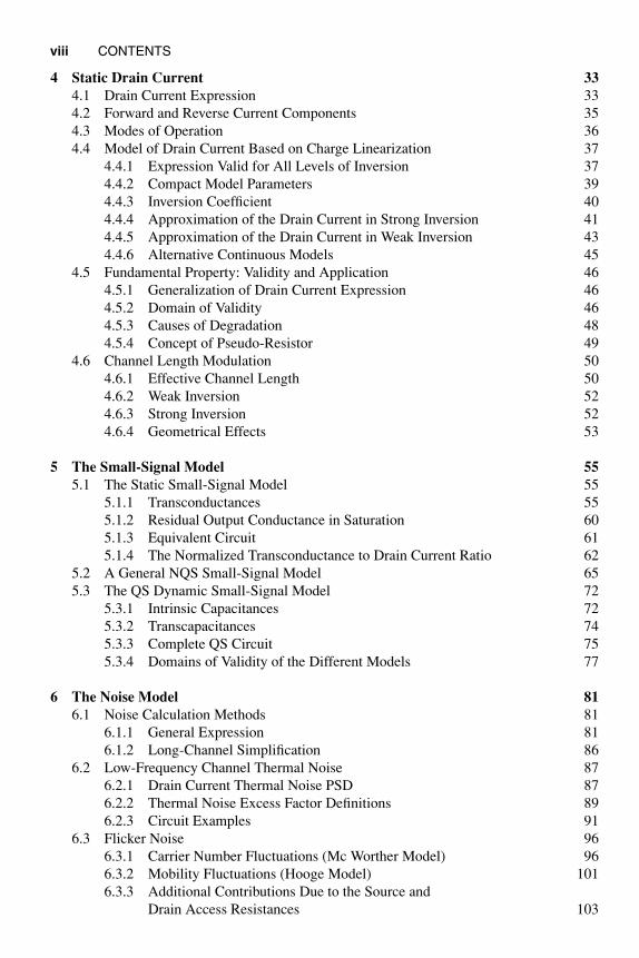
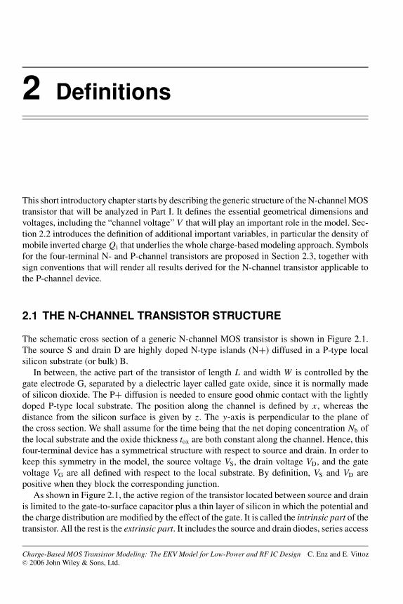
The schematic cross section of a generic N-channel MOS transistor is shown in Figure 2.1.
The source S and drain D are highly doped N-type islands (N+) diffused in a P-type local
silicon substrate (or bulk) B.
In between, the active part of the transistor of length L and width W is controlled by the
gate electrode G, separated by a dielectric layer called gate oxide, since it is normally made
of silicon dioxide. The P+ diffusion is needed to ensure good ohmic contact with the lightly
doped P-type local substrate. The position along the channel is defined by x , whereas the
distance from the silicon surface is given by z. The y-axis is perpendicular to the plane of
the cross section. We shall assume for the time being that the net doping concentration Nb of
the local substrate and the oxide thickness tox are both constant along the channel. Hence, this
four-terminal device has a symmetrical structure with respect to source and drain. In order to
keep this symmetry in the model, the source voltage VS, the drain voltage VD, and the gate
voltage VG are all defined with respect to the local substrate. By definition, VS and VD are
positive when they block the corresponding junction.
As shown in Figure 2.1, the active region of the transistor located between source and drain
is limited to the gate-to-surface capacitor plus a thin layer of silicon in which the potential and
the charge distribution are modified by the effect of the gate. It is called the intrinsic part of the
transistor. All the rest is the extrinsic part. It includes the source and drain diodes, series access
Charge-Based MOS Transistor Modeling: The EKV Model for Low-Power and RF IC Design C. Enz and E. VittozC© 2006 John Wiley & Sons, Ltd.
10 DEFINITIONS
VS
VG
VD
ID
S
G
D
P-type localsubstrate
x
zLwidth W
tox
V
N+N+P+
Intrinsic part
Figure 2.1 Schematic cross section of a MOS transistor
resistors or inductors to the four terminals, and all external parasitic capacitors, in particular
those of the D and S junctions and the direct overlap capacitors from gate electrode to source
and drain islands. This extrinsic part of the device will be discussed in Chapter 10.
Application of a voltage across the source-to-substrate and/or the drain-to-substrate junc-
tions forces electrons and holes out of equilibrium, splitting their respective quasi-Fermi po-
tential by VS at the source end of the channel and VD at the drain end. This splitting propagates
along the channel, and can be characterized by a channel voltage V that varies monotonically
from VS at x = 0 (source end) to VD at x = L (drain end).
Now, for an N-channel device in normal operation (potential increased at the surface by the
voltage applied to the gate), the quasi-Fermi potential of holes can be assumed to be constant
throughout the structure [1,66,67]. Thus V is (within a constant) the quasi-Fermi potential of
electrons in the channel.
Another important voltage is the thermodynamic voltage
UT= kT/q, (2.1)
where k is the Bolzmann constant and q is the elementary charge. Proportional to the absolute
temperature T, it is a measure of the thermal energy of electrons. Since it appears ubiquitously
in MOS modeling equations, it is a more natural unit of voltage for devices and circuits than
the standard unit of 1 V. Its value is 25.8 mV at 300 K or 27 C.
2.2 DEFINITION OF CHARGES, CURRENT, POTENTIAL,AND ELECTRIC FIELDS
For zero electric field at the silicon surface, the source to drain structure of Figure 2.1 corre-
sponds to two back-to-back diodes connected in series; thus, no current other than the junction
leakage current can flow as long as VS and VD are positive. The situation remains qualitatively
the same when more holes are attracted at the surface by applying a negative gate voltage VG.
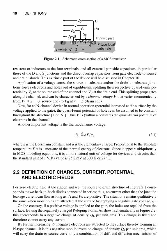
On the contrary, if a positive voltage is applied to the gate, the holes are repelled from the
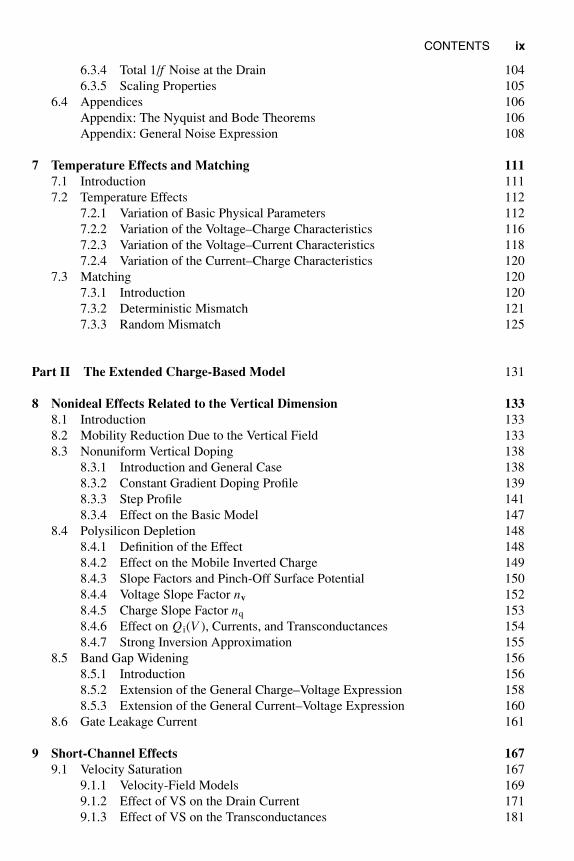
surface, leaving the negatively charged P-doping atoms. As shown schematically in Figure 2.2,
this corresponds to a negative charge of density Qb per unit area. This charge is fixed and
therefore cannot carry any current.
By further increasing VG, negative electrons are attracted to the surface thereby forming an
N-type channel. It is this negative mobile inversion charge, of density Qi per unit area, which
will carry the drain-to-source current by a combination of drift and diffusion mechanisms of
TRANSISTOR SYMBOL AND P-CHANNEL TRANSISTOR 11
Depth z
Charge density (As/m2)
0–tox
–
–
+Depletion charge in bulk Qb
Mobile inversion charge Q i
Fixed interface charge Q fc
Gate charge Qg
Y = Ys
Eox
Figure 2.2 Schematic representation of various local charge densities
electrons. For the N-channel device, this current ID will be defined positive if it enters the drain
terminal.
The charge-based model presented in this book will first calculate the dependency of the
density Qi of induced mobile charge on the voltages applied to the transistor. Then, it will rely
on Qi, and on its particular values QiS and QiD at the source and drain ends of the channel, to
calculate the drain current and to model all aspects of the device behavior.
The total net charge induced underneath the surface of silicon per unit area of channel is
given by
Qsi= Qb + Qi. (2.2)
As depicted in Figure 2.2, an additional component of charge Qfc is present at the silicon-
oxide interface. This is a fixed charge that includes the effect of charges trapped inside the
oxide and weighted by their relative distance to the interface. This charge will be assumed to
be independent of the gate voltage, although it might change very slowly in time at very high
values of gate voltage. Additional voltage-dependent charges due to fast surface state will not
be considered, since they are negligible in modern processes.
The 0-reference of electrostatic potential ψ is that of the bulk of silicon, at a distance from
the surface where it is not affected by the gate voltage. At the silicon surface (z = 0), Ψ takes
the particular value Ψs called the surface potential. The electric field Eox in the oxide depends
on VG − Ψs, but is modified by Φms, the difference between the extraction potentials of gate
and channel materials. It corresponds to the barrier of potential that would be created at their
interface if the oxide thickness tox would be zero. The electric field in the oxide is therefore
given by
Eox =VG − Φms − Ψs
tox
. (2.3)
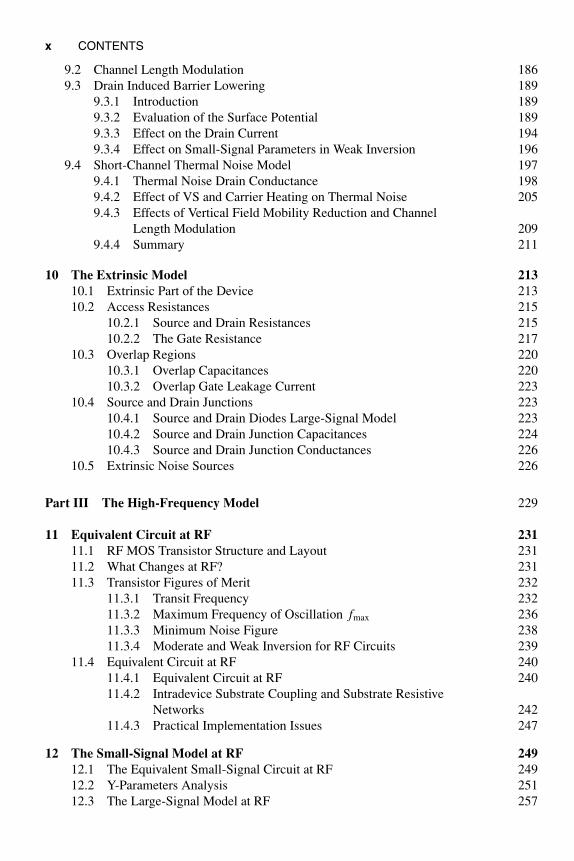
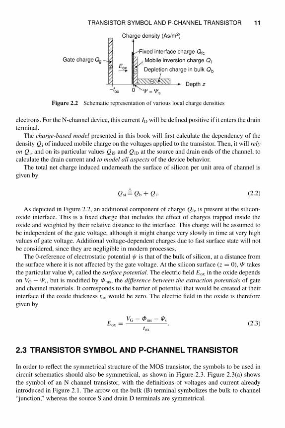
2.3 TRANSISTOR SYMBOL AND P-CHANNEL TRANSISTOR
In order to reflect the symmetrical structure of the MOS transistor, the symbols to be used in
circuit schematics should also be symmetrical, as shown in Figure 2.3. Figure 2.3(a) shows
the symbol of an N-channel transistor, with the definitions of voltages and current already
introduced in Figure 2.1. The arrow on the bulk (B) terminal symbolizes the bulk-to-channel
“junction,” whereas the source S and drain D terminals are symmetrical.
12 DEFINITIONS
VG
VS VD
IDS D
G
B
(a) N-channel
VG
VSVD
ID SD
G
B
(b) P-channel
Figure 2.3 Symbols and definitions for N-channel and P-channel MOS transistors
The generic structure of a P-channel transistor is similar to that of the N-channel, but the
doping types are opposite, with P+ source and drain diffusions inside an N-type local substrate
(which is usually an N-well in modern processes). Hence a negative voltage must be applied
to the gate to obtain a positive inverted charge of holes Qi, after creating a positive depletion
charge Qb.
In spite of this sign difference, all equations that will be derived for modeling the N-channel
transistor will be applicable to the P-channel device, provided the definitions of positive voltages
and currents are inverted, as shown in Figure 2.3(b). The arrow in the bulk connection is
inverted, which might be sufficient to distinguish it from the N-channel. However, since very
often the bulk connection is the same for all transistors of the same type and is therefore not
represented, a small circle is added at the gate of the P-channel device.
It should be pointed out that, except for the gate electrode, the generic structure illustrated
in Figure 2.1 is also that of an NPN lateral bipolar transistor. Indeed, this parasitic transistor
will be activated as soon as one of the two junctions is sufficiently forward biased (−VS and/or
−VD larger than a few hundred millivolts). This device may be exploited as a true bipolar
transistor, provided it is in a separate well (which becomes the base of the transistor) and the
MOS current is canceled by a negative gate voltage [68]. This special mode of operation will
not be further discussed in this book.
3 The Basic Charge Model
This chapter is dedicated to the calculation and the modeling of the density of induced mobile
charge Qi as a function of the various voltages applied to the transistor. Section 3.1 is a repetition
of the classical one-dimensional analysis of the total charge density Qsi induced at the surface
of a long transistor channel by a nonzero surface potential. It already shows the fundamental
difference between weak and strong inversion. This difference is further highlighted by the
dependency of the surface potential on the gate voltage, which is derived in Section 3.2. Section
3.3 takes advantage of the results obtained so far to calculate the variation of the local gate
capacitance per unit area as a function of the gate voltage and the local channel voltage. Section
3.4 introduces and justifies the charge sheet approximation, which will be used throughout the
rest of the book. Using this approximation, Qi is then obtained in Section 3.5 by the difference
between the gate voltage and a threshold function VTB of the surface potential Ψs, and it
cancels at a value called pinch-off surface potential ΨP. The slope n of VTB(Ψs) will become
one of the few basic parameters of the model. In Section 3.6, an important simplification of
the model is introduced by exploiting the fact that this slope n may be considered constant,
which corresponds to a linearization of the charge versus potential relationship. Based on this
linearization, an explicit expression is obtained that relates Qi to the channel voltage V, within
a constant called pinch-off (channel) voltage VP. This expression is normalized and depends
only on process parameters through a specific charge Qspec. By using an approximation of this
expression in strong inversion, a threshold voltage (at equilibrium) VT0 is defined, by which
VP can then be directly related to the gate voltage.
3.1 POISSON’S EQUATION AND GRADUALCHANNEL APPROXIMATION
In the P-type substrate of an N-channel MOS transistor, the total charge concentration ρ is the
net effect of the concentrations Nb of doping atoms, of holes pp and np of electrons:
ρ = q(pp − np − Nb). (3.1)
Charge-Based MOS Transistor Modeling: The EKV Model for Low-Power and RF IC Design C. Enz and E. VittozC© 2006 John Wiley & Sons, Ltd.
14 THE BASIC CHARGE MODEL
Far from the surface, the semiconductor is neutral, and ρ = 0. Closer to the surface, the
spatial variations of potential Ψ due to the electric field produced by the gate result in a nonzero
charge concentration according to the three-dimensional Poisson’s equation
∂2Ψ
∂x2+
∂2Ψ
∂y2+
∂2Ψ
∂z2= −
ρ
ǫsi
, (3.2)
where ǫsi is the dielectric constant of silicon.
The channel is long and wide compared to the oxide thickness tox, allowing the gradual
channel approximation, stating that the electric field variation in the z-direction (perpendicular
to the surface) is much larger than that in the x- and y-directions. Therefore, the second
derivative of potential Ψ in the directions parallel to the surface can be neglected in (3.2), and
this three-dimensional equation can be reduced to the one-dimensional equation in z:
d2Ψ
dz2=
q
ǫsi
(np − pp + Nb). (3.3)
For an N-channel transistor, the quasi-Fermi potential of holes can be assumed to be constant
for Ψ ≥ 0 [1, 66, 67]. The hole concentration can therefore be expressed as
pp = ni expΦF − Ψ
UT
, (3.4)
where ni is the intrinsic carrier concentration and ΦF is the Fermi potential of the silicon
substrate. At T = 300 K, ni = 1.45 × 1010 cm−3.
Application of a source voltage VS and/or a drain voltage VD brings the electrons in the
channel out of equilibrium, which is characterized by a quasi-Fermi potential ΦFn different
from ΦF. As explained in the introduction, this difference is called channel voltage V, and
ΦFn = ΦF + V . The concentration of electrons can thus be expressed as
np = ni expΨ − ΦFn
UT
= ni expΨ − ΦF − V
UT
. (3.5)
The doping concentration Nb is assumed to be constant in the channel region. Far from the
surface, the effect of VS, VD, and Eox vanishes; thus V = Ψ = 0, and the silicon is neutral
with ρ = 0. Combining equations (3.1), (3.4), and (3.5) then yields
Nb = ni
(
expΦF
UT
− exp−ΦF
UT
)
∼= ni expΦF
UT
(3.6)
since ΦF ≫ UT, resulting in
ni = Nb exp−ΦF
UT
. (3.7)
POISSON’S EQUATION AND GRADUAL CHANNEL APPROXIMATION 15
The expression relating the Fermi potential ΦF to the doping concentration Nb is then given
by
ΦF = UT lnNb
ni
. (3.8)
Introducing (3.4), (3.5), and (3.7) in (3.3) yields
d2Ψ
dz2=
q Nb
ǫsi
⎛
⎜⎜⎝
expΨ − 2ΦF − V
UT︸ ︷︷ ︸
electrons
− exp−Ψ
UT︸ ︷︷ ︸
holes
+1︸︷︷︸
fixed charge
⎞
⎟⎟⎠
q Nb
ǫsi
G(Ψ, 2ΦF + V ). (3.9)
The first term in the parentheses is the contribution of electrons, the second that of holes, and
the third that of the fixed depletion charge.
Now, the vertical field is given by
Ez = −dΨ
dz; (3.10)
hence,
d2Ψ
dz2= −
dEz
dz= −
dEz
dΨ
dΨ
dz= Ez
dEz
dΨ(3.11)
and Poisson’s equation (3.9) becomes
Ez dEz =q Nb
ǫsi
G(Ψ, 2ΦF + V ) dΨ. (3.12)
Both sides of this equation can now be integrated from far below the surface, where Ez = 0
and Ψ = 0, to closer to the surface where they become nonzero:
∫ Ez
0
Ez dEz =E2
z
2=
q Nb
ǫsi
∫ Ψ
0
G(Ψ, 2ΦF + V ) dΨ. (3.13)
This finally yields the vertical field Ez as a function of Ψ and V :
Ez = sgn(Ψ )UT
LD
F(Ψ, 2ΦF + V ), (3.14)
where LD is a combination of constants called the extrinsic Debye length
LD
√
ǫsiUT
2q Nb
(3.15)
16 THE BASIC CHARGE MODEL
FF =14UT
Accum
ulation
V/UTY = 2FF10
3
20 40 60–20
10
102
10–1
1
10–2
Weak inv.
Stron
g in
v.
UT
V = 0 V > 0
Ys
Ys
UT
F
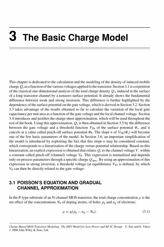
Figure 3.1 Function F relating Ez to Ψ , and Ezs and Qsi to Ψs
and
F(Ψ, 2ΦF + V ) √√√√√
(
expΨ
UT
− 1
)
exp−(2ΦF + V )
UT︸ ︷︷ ︸
contribution of electrons
+(
exp−Ψ
UT
− 1
)
︸ ︷︷ ︸
of holes
+Ψ
UT︸ ︷︷ ︸
of fixed charge
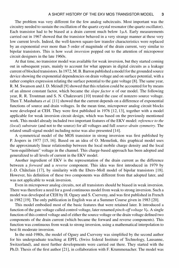
. (3.16)
This function is represented in Figure 3.1 for ΦF = 14UT, which, according to (3.8), corre-
sponds at ambient temperature to a doping concentration Nb of 1.7 × 1016 cm−3. At the surface
of silicon, the potential Ψ takes the value Ψs, and the vertical field has the value Ezs given
by F(Ψs, 2ΦF + V ). Knowing the surface field, the local silicon charge density Qsi can be
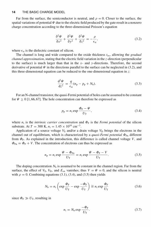
obtained by applying Gauss’ law to a short section of channel, as explained by Figure 3.2.
A parallelepiped volume of channel starts at the surface of silicon where Ez = Ezs and
ends deep in the substrate where Ez = 0; according to the gradual channel approximation, the
variation of horizontal field along a short section of channel is negligible; thus, Ex+Δx = Ex .
Finally, the lateral field Ey = 0 so that the only side contributing to the electrical flux leaving
the volume is the surface. According to Gauss’ law, this flux is equal to the net charge inside
–Ezs
∆x << L
Unit area of channel
Ex+∆x = Ex
Ey = 0Ez = 0
Qsi
Ex
Figure 3.2 Application of Gauss’ law to calculate Qsi from the surface field Ezs
SURFACE POTENTIAL AS A FUNCTION OF GATE VOLTAGE 17
the volume, which is equal to Qsi for a unit area of channel. Thus, for Ψs > 0,
Qsi = −ǫsi Ezs = −ǫsiUT
LD
F(Ψs, 2ΦF + V ). (3.17)
For a given value of 2ΦF + V, the function F plotted in Figure 3.1 thus represents Ez(Ψ ),
Ezs(Ψs), and Qsi(Ψs). It results from the contribution of the three types of charge, which can
still be identified inside the square root of (3.16): the first term is the contribution of electrons,
the second that of holes (which become negligible for Ψ ≫ UT), and the third term that of the
fixed depletion charge.
For negative values of Ψs, the second term dominates and holes accumulate exponentially. If
Ψs = 0 then F = 0; the silicon is neutral up to the surface. This is called the flat-band situation.
For 0 < Ψs ≪ 2ΦF + V, the last term due to the fixed depletion charge dominates. The
small quantity of electrons corresponding to the second term is negligible in the calculation of
field and total charge, but will be the only charge available to transport current. This situation
is called weak inversion.
When Ψs exceeds 2ΦF + V, the first term becomes nonnegligible and would keep its expo-
nential growth if Ψs could be increased much above. This situation is called strong inversion.
It must be pointed out that F is a nonlinear function of the three kinds of charge, and so
neither Qi nor Qb can be identified separately in this function, except if one of them strongly
dominates. This is the case in weak inversion where, from (3.17) and (3.16),
Qsi∼= Qb = −
ǫsiUT
LD
√
Ψs
UT
(weak inversion). (3.18)
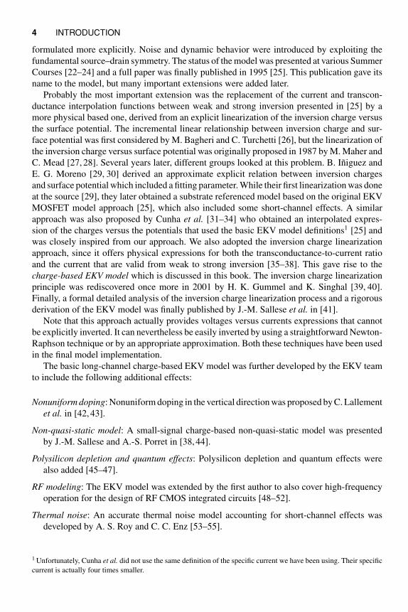
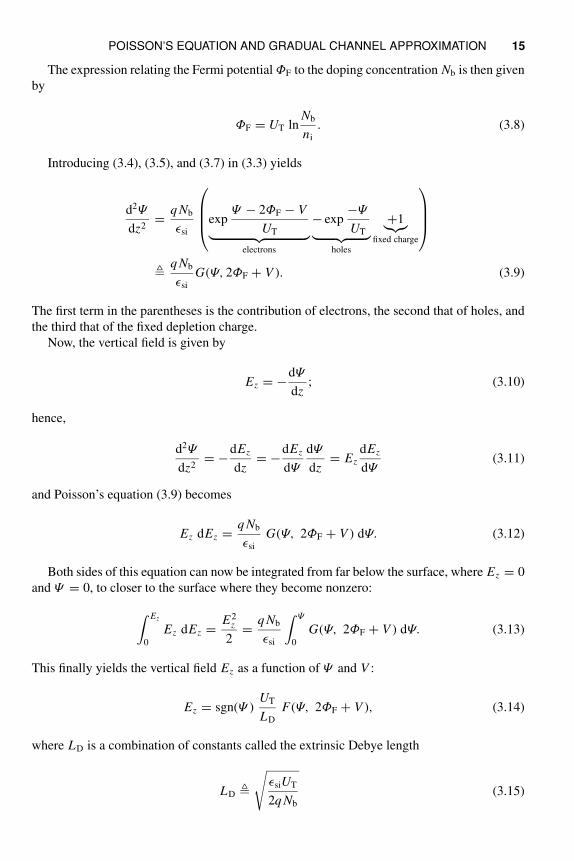
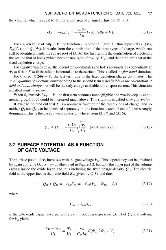
3.2 SURFACE POTENTIAL AS A FUNCTIONOF GATE VOLTAGE
The surface potential Ψs increases with the gate voltage VG. This dependency can be obtained
by again applying Gauss’ law as illustrated in Figure 3.2, but with the upper part of the volume
ending inside the oxide layer, and thus including the fixed charge density Qfc. The electric
field at the upper face is the oxide field Eox given by (2.3), and thus
Qsi + Qfc = −ǫox Eox = −Cox(VG − Φms − Ψs), (3.19)
where
Cox = ǫox/tox (3.20)
is the gate oxide capacitance per unit area. Introducing expression (3.17) of Qsi and solving
for VG yields
VG − VFB
UT
=Ψs
UT
+ǫsi
CoxLD
F(Ψs, 2ΦF + V ), (3.21)
18 THE BASIC CHARGE MODEL
V = 0
V > 0
0 20 40 60 80 100 120 1400
20
40
60
V/U T
εsi
CoxLD
= 5= 14;
UT
Ys
U T
2FF + V
2FF
Strong inversion
Weak in
version
U T
U T FF
U T
VG – VFB
Figure 3.3 Surface potential Ψs as a function of gate voltage VG
where VFB is the flat-band voltage given by
VFB Φms +−Qfc
Cox
. (3.22)
It is the value of the gate voltage VG needed to obtain the flat-band situation, for which Ψs = 0
and Qsi = 0.
Relation (3.21) is represented in Figure 3.3 for realistic particular values of ΦF and
ǫsi/(CoxLD).
As long as Ψs ≪ 2ΦF + V (corresponding to weak inversion), Qsi = Qb increases only
with the square root of Ψs. Thus Ψs increases with VG. But as soon as Ψs reaches 2ΦF + V, Qsi
starts increasing much more rapidly with Ψs due to the important contribution of mobile charge.
This is not compatible with the limited field, and thus the surface potential only increases very
slowly to become almost constant in strong inversion.
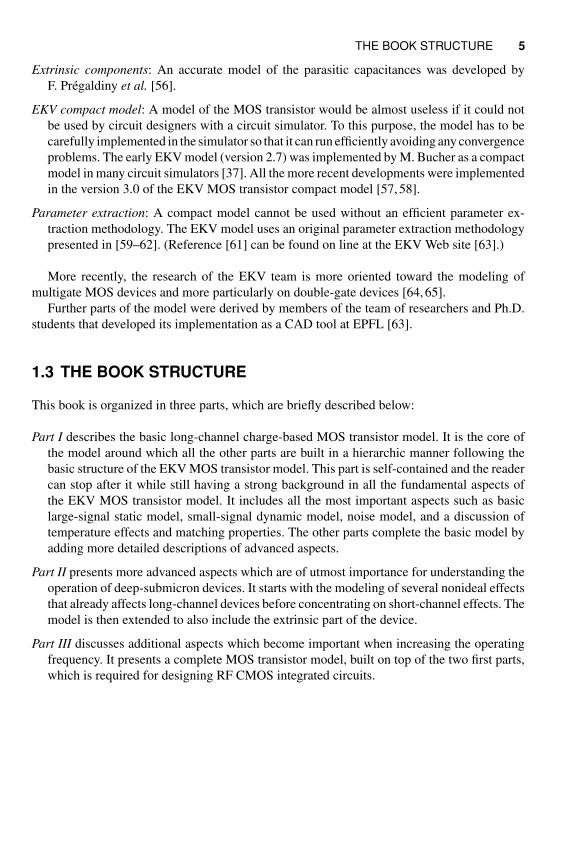
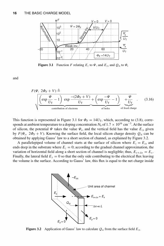
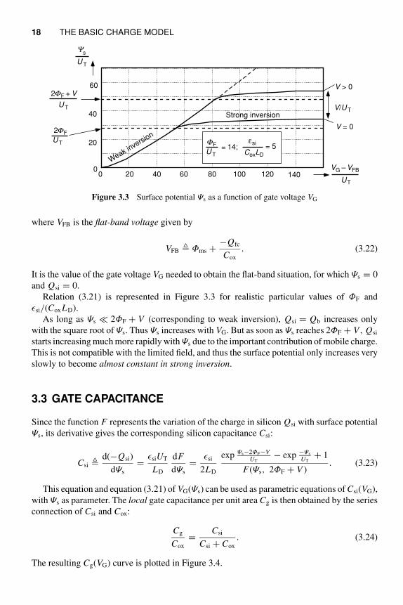
3.3 GATE CAPACITANCE
Since the function F represents the variation of the charge in silicon Qsi with surface potential
Ψs, its derivative gives the corresponding silicon capacitance Csi:
Csi d(−Qsi)
dΨs
=ǫsiUT
LD
dF
dΨs
=ǫsi
2LD
exp Ψs−2ΦF−VUT
− exp −Ψs
UT+ 1
F(Ψs, 2ΦF + V ). (3.23)
This equation and equation (3.21) of VG(Ψs) can be used as parametric equations of Csi(VG),
with Ψs as parameter. The local gate capacitance per unit area Cg is then obtained by the series
connection of Csi and Cox:
Cg
Cox
=Csi
Csi + Cox
. (3.24)
The resulting Cg(VG) curve is plotted in Figure 3.4.
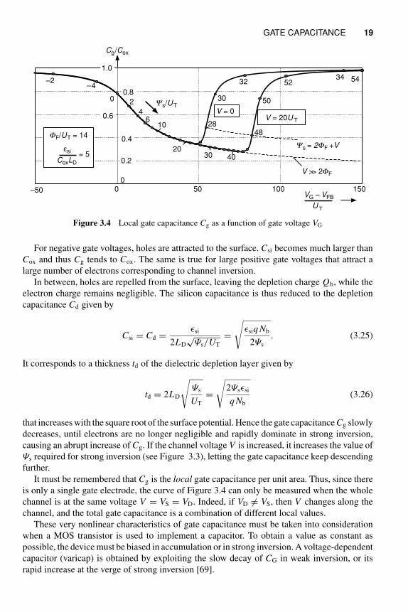
GATE CAPACITANCE 19
0
–2–4
2
050 100 150
46
10
20
28
30
3234
40
48
50
52 54
30
0.6
0.8
0.4
0.2
0
1.0
–50VG – VFB
U T
Cg/Cox
Ys/UT
Ys = 2FF +V
V >> 2FF
V = 0V = 20U T
FF/UT = 14
εsi
CoxLD
= 5
Figure 3.4 Local gate capacitance Cg as a function of gate voltage VG
For negative gate voltages, holes are attracted to the surface. Csi becomes much larger than
Cox and thus Cg tends to Cox. The same is true for large positive gate voltages that attract a
large number of electrons corresponding to channel inversion.
In between, holes are repelled from the surface, leaving the depletion charge Qb, while the
electron charge remains negligible. The silicon capacitance is thus reduced to the depletion
capacitance Cd given by
Csi = Cd =ǫsi
2LD
√Ψs/UT
=
√
ǫsiq Nb
2Ψs
. (3.25)
It corresponds to a thickness td of the dielectric depletion layer given by
td = 2LD
√
Ψs
UT
=
√
2Ψsǫsi
q Nb
(3.26)
that increases with the square root of the surface potential. Hence the gate capacitance Cg slowly
decreases, until electrons are no longer negligible and rapidly dominate in strong inversion,
causing an abrupt increase of Cg. If the channel voltage V is increased, it increases the value of
Ψs required for strong inversion (see Figure 3.3), letting the gate capacitance keep descending
further.
It must be remembered that Cg is the local gate capacitance per unit area. Thus, since there
is only a single gate electrode, the curve of Figure 3.4 can only be measured when the whole
channel is at the same voltage V = VS = VD. Indeed, if VD = VS, then V changes along the
channel, and the total gate capacitance is a combination of different local values.
These very nonlinear characteristics of gate capacitance must be taken into consideration
when a MOS transistor is used to implement a capacitor. To obtain a value as constant as
possible, the device must be biased in accumulation or in strong inversion. A voltage-dependent
capacitor (varicap) is obtained by exploiting the slow decay of CG in weak inversion, or its
rapid increase at the verge of strong inversion [69].
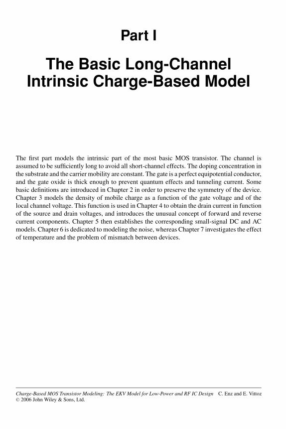
20 THE BASIC CHARGE MODEL
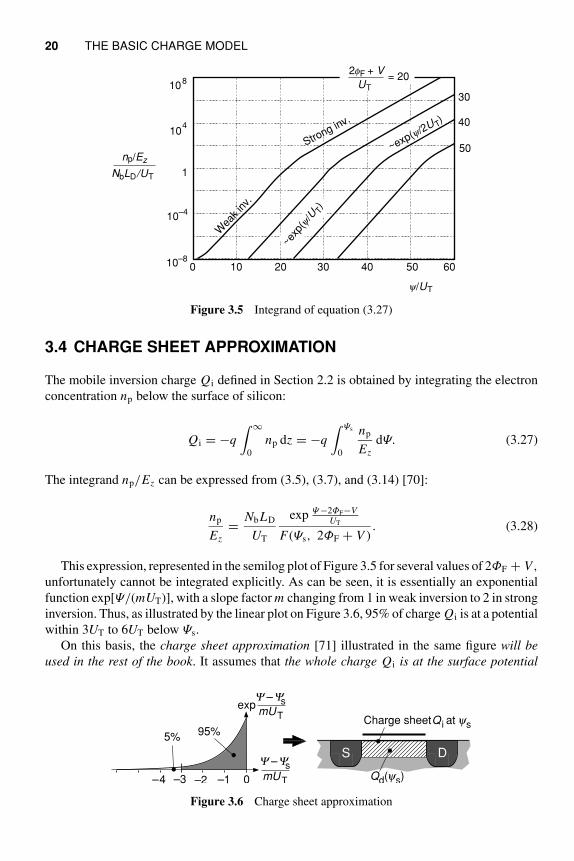
~exp
(y/U
T)
605040302010010–8
10–4
1
104
108
2fF + V
UT
= 20
30
40
50
Wea
k in
v.
Strong in
v.
y/UT
np/Ez
NbLD/UT
~exp(y/2U T)
Figure 3.5 Integrand of equation (3.27)
3.4 CHARGE SHEET APPROXIMATION
The mobile inversion charge Qi defined in Section 2.2 is obtained by integrating the electron
concentration np below the surface of silicon:
Qi = −q
∫ ∞
0
np dz = −q
∫ Ψs
0
np
Ez
dΨ. (3.27)
The integrand np/Ez can be expressed from (3.5), (3.7), and (3.14) [70]:
np
Ez
=NbLD
UT
exp Ψ −2ΦF−VUT
F(Ψs, 2ΦF + V ). (3.28)
This expression, represented in the semilog plot of Figure 3.5 for several values of 2ΦF + V,
unfortunately cannot be integrated explicitly. As can be seen, it is essentially an exponential
function exp[Ψ/(mUT)], with a slope factor m changing from 1 in weak inversion to 2 in strong
inversion. Thus, as illustrated by the linear plot on Figure 3.6, 95% of charge Qi is at a potential
within 3UT to 6UT below Ψs.
On this basis, the charge sheet approximation [71] illustrated in the same figure will be
used in the rest of the book. It assumes that the whole charge Qi is at the surface potential
–3
95%
0–1–2–4 mUT
exp
5%
Y – Ys
Y – Ys
mUT Charge sheet Q i at ys
DS
Qd(ys)
Figure 3.6 Charge sheet approximation

DENSITY OF MOBILE INVERTED CHARGE 21
Ψs. Thus, since there is no voltage drop across this thin charge sheet, the depletion charge Qb
is controlled by Ψs. Hence, it can be approximated by expression (3.18) for weak inversion
(where Qi is really negligible):
−Qb =ǫsiUT
LD
√
Ψs
UT
= ΓbCox
√
Ψs, (3.29)
where Γb is the substrate modulation factor, given by
Γb ǫsi
LDCox
√
UT =√
2q Nbǫsi
Cox
. (3.30)
3.5 DENSITY OF MOBILE INVERTED CHARGE
3.5.1 Mobile Charge as a Function of Gate Voltageand Surface Potential
The total charge density Qsi can be calculated from the field in the oxide by using relations
(3.19) and (3.22),
Qsi = −Cox(VG − VFB − Ψs), (3.31)
and, with the charge sheet approximation, the depletion charge Qb is given by (3.29). Although
the inversion charge Qi cannot be explicitly obtained directly from (3.27), it can be expressed
as their difference
Qi = Qsi − Qb = −Cox(VG − VFB − Ψs − Γb
√
Ψs) = −Cox(VG − VTB), (3.32)
where
VTB VFB + Ψs + Γb
√
Ψs (3.33)
is the threshold function. This function of Ψs that depends on the process through parameters
VFB and Γb is represented in Figure 3.7 for two extreme values of Γb.
This function is nonlinear due to the contribution of Qb and its slope n > 1 is obtained by
differentiation of (3.33):
n dVTB
dΨs
= 1 +Γb
2√
Ψs
. (3.34)
It is represented in Figure 3.8.
As can be seen, n is a very slow function of Ψs, especially since in normal situations, Ψs is
not lower than about 20UT. Its maximum value thus ranges between 1.2 and 1.7, and it tends
to 1 for very large values of Ψs.
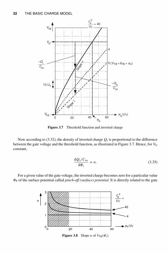
22 THE BASIC CHARGE MODEL
Slo
pe n
–Qi
Cox
VG
4
VTB
(UT)VFB
–Qb
Cox
Slope
1
0 20 40 60
10 UT
yP
0
Gb
UT
= 40
2
yS
(VTB =VFB + ys)
Figure 3.7 Threshold function and inverted charge
Now according to (3.32), the density of inverted charge Qi is proportional to the difference
between the gate voltage and the threshold function, as illustrated in Figure 3.7. Hence, for VG
constant,
dQi/Cox
dΨs
= n. (3.35)
For a given value of the gate voltage, the inverted charge becomes zero for a particular value
ΨP of the surface potential called pinch-off (surface) potential. It is directly related to the gate
4
0 20 40 60ys/UT0
1
2
3
n
40
Gb
UT
=
2
Figure 3.8 Slope n of VTB(Ψs)
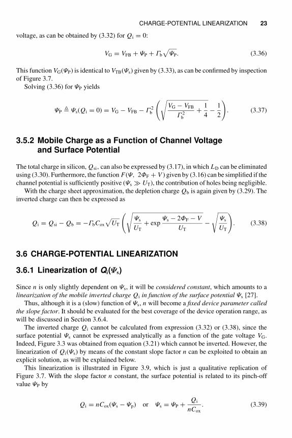
CHARGE-POTENTIAL LINEARIZATION 23
voltage, as can be obtained by (3.32) for Qi = 0:
VG = VFB + ΨP + Γb
√
ΨP. (3.36)
This function VG(ΨP) is identical to VTB(Ψs) given by (3.33), as can be confirmed by inspection
of Figure 3.7.
Solving (3.36) for ΨP yields
ΨP Ψs(Qi = 0) = VG − VFB − Γ 2b
(√
VG − VFB
Γ 2b
+1
4−
1
2
)
. (3.37)
3.5.2 Mobile Charge as a Function of Channel Voltageand Surface Potential
The total charge in silicon, Qsi, can also be expressed by (3.17), in which LD can be eliminated
using (3.30). Furthermore, the function F(Ψ, 2ΦF + V ) given by (3.16) can be simplified if the
channel potential is sufficiently positive (Ψs ≫ UT), the contribution of holes being negligible.
With the charge sheet approximation, the depletion charge Qb is again given by (3.29). The
inverted charge can then be expressed as
Qi = Qsi − Qb = −ΓbCox
√
UT
(√
Ψs
UT
+ expΨs − 2ΦF − V
UT
−
√
Ψs
UT
)
. (3.38)
3.6 CHARGE-POTENTIAL LINEARIZATION
3.6.1 Linearization of Qi(Ψs)
Since n is only slightly dependent on Ψs, it will be considered constant, which amounts to a
linearization of the mobile inverted charge Qi in function of the surface potential Ψs [27].
Thus, although it is a (slow) function of Ψs, n will become a fixed device parameter called
the slope factor. It should be evaluated for the best coverage of the device operation range, as
will be discussed in Section 3.6.4.
The inverted charge Qi cannot be calculated from expression (3.32) or (3.38), since the
surface potential Ψs cannot be expressed analytically as a function of the gate voltage VG.
Indeed, Figure 3.3 was obtained from equation (3.21) which cannot be inverted. However, the
linearization of Qi(Ψs) by means of the constant slope factor n can be exploited to obtain an
explicit solution, as will be explained below.
This linearization is illustrated in Figure 3.9, which is just a qualitative replication of
Figure 3.7. With the slope factor n constant, the surface potential is related to its pinch-off
value ΨP by
Qi = nCox(Ψs − Ψp) or Ψs = ΨP +Qi
nCox
. (3.39)
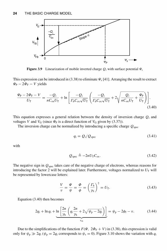
24 THE BASIC CHARGE MODEL
–Qi
Cox
VG
VTB
ys
VFB
0y
P
Slope n
Figure 3.9 Linearization of mobile inverted charge Qi with surface potential Ψs
This expression can be introduced in (3.38) to eliminate Ψs [41]. Arranging the result to extract
ΨP − 2ΦF − V yields
ΨP − 2ΦF − V
UT
=−Qi
nCoxUT
+ ln
[
−Qi
ΓbCox
√UT
(
−Qi
ΓbCox
√UT
+ 2
√
Qi
nCoxUT
+ΨP
UT
)]
.
(3.40)
This equation expresses a general relation between the density of inversion charge Qi and
voltages V and VG (since ΨP is a direct function of VG given by (3.37)).
The inversion charge can be normalized by introducing a specific charge Qspec
qi = Qi/Qspec (3.41)
with
Qspec −2nUTCox. (3.42)
The negative sign in Qspec takes care of the negative charge of electrons, whereas reasons for
introducing the factor 2 will be explained later. Furthermore, voltages normalized to UT will
be represented by lowercase letters:
V
v=
Ψ
ψ=
Φ
φ=
(Γb
γb
)2
= UT. (3.43)
Equation (3.40) then becomes
2qi + ln qi + ln
[2n
γb
(
qi
2n
γb
+ 2√
ψp − 2qi
)]
︸ ︷︷ ︸
vsh
= ψp − 2φf − v. (3.44)
Due to the simplifications of the function F(Ψ, 2ΦF + V ) in (3.38), this expression is valid
only for ψp ≫ 2qi (ψp = 2qi corresponds to ψs = 0). Figure 3.10 shows the variation with qi
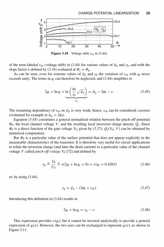
CHARGE-POTENTIAL LINEARIZATION 25
100;2
30;2
100;7
30;7
60;4
0 10 20 30 40 501
2
3
4
yp ; gb
q i
vsh
Voltage s
hift
Figure 3.10 Voltage shift vsh in (3.44).
of the term labeled vsh (voltage shift) in (3.44) for various values of ψp and γb, and with the
slope factor n defined by (3.34) evaluated at Ψs = Ψp.
As can be seen, even for extreme values of ψp and γb the variation of vsh with qi never
exceeds unity. The terms in qi can therefore be neglected, and (3.44) simplifies to
2qi + ln qi + ln
(4n
γb
√
ψp
)
︸ ︷︷ ︸
vsh
= ψp − 2φf − v. (3.45)
The remaining dependency of vsh on ψp is very weak; hence, vsh can be considered constant
(evaluated for example at ψp = 2φf).
Equation (3.45) constitutes a general normalized relation between the pinch-off potential
ΨP, the local channel voltage V , and the resulting local inversion charge density Qi. Since
ΨP is a direct function of the gate voltage VG given by (3.37), Qi(VG, V ) can be obtained by
numerical computation.
But ΨP is a particular value of the surface potential that does not appear explicitly in the
measurable characteristics of the transistor. It is therefore very useful for circuit applications
to relate the inversion charge (and later the drain current) to a particular value of the channel
voltage V called pinch-off voltage VP [72] and defined by
vp VP
UT
v(2qi + ln qi = 0) = v(qi = 0.4263) (3.46)
or, by using (3.44),
vp = ψp − (2φf + vsh). (3.47)
Introducing this definition in (3.44) results in
2qi + ln qi = vp − v. (3.48)
This expression provides v(qi), but it cannot be inverted analytically to provide a general
expression of qi(v). However, the two axes can be exchanged to represent qi(v), as shown in
Figure 3.11.
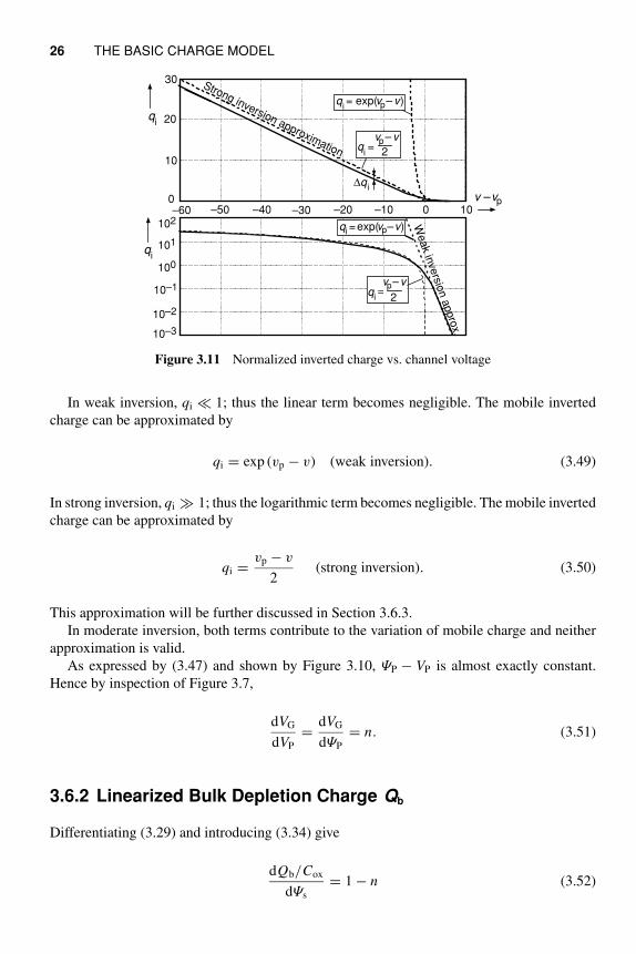
26 THE BASIC CHARGE MODEL
qi=
vp– v
2
0 10–20–30–40–50–60 –10
10
20
30
0
qi= exp(vp– v)
v –vp
qi
100
101
10–3
10–2
10–1
102
qi
qi = exp(vp–v)
qi=vp– v
2
Strong inversion approximation
Weak in
versio
n a
ppro
x.∆q i
Figure 3.11 Normalized inverted charge vs. channel voltage
In weak inversion, qi ≪ 1; thus the linear term becomes negligible. The mobile inverted
charge can be approximated by
qi = exp (vp − v) (weak inversion). (3.49)
In strong inversion, qi ≫ 1; thus the logarithmic term becomes negligible. The mobile inverted
charge can be approximated by
qi =vp − v
2(strong inversion). (3.50)
This approximation will be further discussed in Section 3.6.3.
In moderate inversion, both terms contribute to the variation of mobile charge and neither
approximation is valid.
As expressed by (3.47) and shown by Figure 3.10, ΨP − VP is almost exactly constant.
Hence by inspection of Figure 3.7,
dVG
dVP
=dVG
dΨP
= n. (3.51)
3.6.2 Linearized Bulk Depletion Charge Qb
Differentiating (3.29) and introducing (3.34) give
dQb/Cox
dΨs
= 1 − n (3.52)
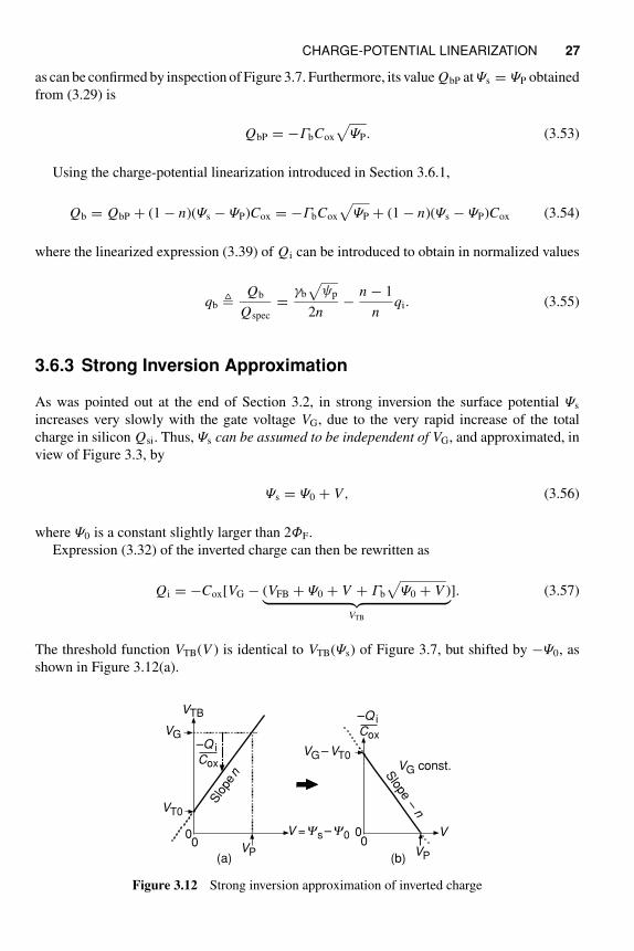
CHARGE-POTENTIAL LINEARIZATION 27
as can be confirmed by inspection of Figure 3.7. Furthermore, its value QbP at Ψs = ΨP obtained
from (3.29) is
QbP = −ΓbCox
√
ΨP. (3.53)
Using the charge-potential linearization introduced in Section 3.6.1,
Qb = QbP + (1 − n)(Ψs − ΨP)Cox = −ΓbCox
√
ΨP + (1 − n)(Ψs − ΨP)Cox (3.54)
where the linearized expression (3.39) of Qi can be introduced to obtain in normalized values
qb Qb
Qspec
=γb
√ψp
2n−
n − 1
nqi. (3.55)
3.6.3 Strong Inversion Approximation
As was pointed out at the end of Section 3.2, in strong inversion the surface potential Ψs
increases very slowly with the gate voltage VG, due to the very rapid increase of the total
charge in silicon Qsi. Thus, Ψs can be assumed to be independent of VG, and approximated, in
view of Figure 3.3, by
Ψs = Ψ0 + V, (3.56)
where Ψ0 is a constant slightly larger than 2ΦF.
Expression (3.32) of the inverted charge can then be rewritten as
Qi = −Cox[VG − (VFB + Ψ0 + V + Γb
√
Ψ0 + V )︸ ︷︷ ︸
VTB
]. (3.57)
The threshold function VTB(V ) is identical to VTB(Ψs) of Figure 3.7, but shifted by −Ψ0, as
shown in Figure 3.12(a).
Slo
pe n
VG
VTB
V = Ys– Y0
VP
–Q iCox
VT0
0
(a)
Slope – n
V
VP
–Q iCox
VG – VT0
0
VG const.
(b)
0 0
Figure 3.12 Strong inversion approximation of inverted charge
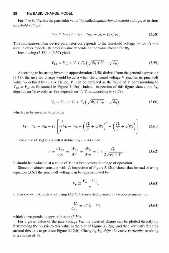
28 THE BASIC CHARGE MODEL
For V = 0, VTB has the particular value VT0 called equilibrium threshold voltage, or in short
threshold voltage:
VT0 VTB(V = 0) = VFB + Ψ0 + Γb
√
Ψ0. (3.58)
This bias-independent device parameter corresponds to the threshold voltage VT for VS = 0
used in other models. Its precise value depends on the value chosen for Ψ0.
Introducing (3.58) in (3.57) yields
VTB = VT0 + V + Γb
(√
Ψ0 + V −√
Ψ0
)
. (3.59)
According to its strong inversion approximation (3.50) derived from the general expression
(3.48), the inverted charge would be zero when the channel voltage V reaches its pinch-off
value VP defined by (3.46). Hence, VP can be obtained as the value of V corresponding to
VTB = VG, as illustrated in Figure 3.12(a). Indeed, inspection of this figure shows that VG
depends on VP exactly as VTB depends on V . Thus according to (3.59),
VG = VT0 + VP + Γb
(√
Ψ0 + VP −√
Ψ0
)
, (3.60)
which can be inverted to provide
VP = VG − VT0 − Γb
⎡
⎣
√
VG − VT0 +(
Γb
2+
√
Ψ0
)2
−(
Γb
2+
√
Ψ0
)⎤
⎦. (3.61)
The slope of VG(VP) is still n defined by (3.34) since
n =dVTB
dΨs
=dVTB
dV=
dVG
dVP
= 1 +Γb
2√
Ψ0 + V. (3.62)
It should be evaluated at a value of V that best covers the range of operation.
Since n is almost constant with V , inspection of Figure 3.12(a) shows that instead of using
equation (3.61) the pinch-off voltage can be approximated by
VP∼=
VG − VT0
n. (3.63)
It also shows that, instead of using (3.57), the inverted charge can be approximated by
−Qi
Cox
= n(VP − V ), (3.64)
which corresponds to approximation (3.50).
For a given value of the gate voltage VG, the inverted charge can be plotted directly by
first moving the V -axis to this value in the plot of Figure 3.12(a), and then vertically flipping
around this axis to produce Figure 3.12(b). Changing VG shifts the curve vertically, resulting
in a change of VP.
CHARGE-POTENTIAL LINEARIZATION 29
0
10
20
0 20 40 60 80 100
∆q i /q i(%)
q i
Figure 3.13 Relative error of inverted charge in strong inversion approximation
By introducing expression (3.58) of VT0 into (3.61) and comparing the result with expression
(3.37) of ΨP, we obtain
VP = ΨP − Ψ0. (3.65)
Hence, according to (3.47)
ψ0 = ψp − vp = 2φf + vsh or Ψ0 = Ψp − Vp = 2ΦF + Vsh. (3.66)
Inspection of Figure 3.10 shows that vsh is almost constant, whereas Figure 3.3 shows that
the surface potential keeps increasing slowly in strong inversion. This difference is due to the
logarithmic term in (3.48), which has been neglected in approximation (3.50). It results in a dif-
ference Δqi of the inverted charge qi that is represented in relative values in Figure 3.13. As can
be seen, the excess of charge obtained in the strong inversion approximation never exceeds 18%.
Notice that although the threshold voltage VT0 was introduced in the framework of this
strong inversion approximation, it can always be used to relate VP to VG by equation (3.61) or
by its approximation (3.63).
3.6.4 Evaluation of the Slope Factor
As already stated in Section 3.6.1, the slope factor n defined by (3.34) should be evaluated to
best fit the range of operation of the transistor.
Inspection of Figure 3.9 shows that n would be best evaluated as the slope of the secant of
the threshold function VTB between a particular value of surface potential Ψs and its pinch-off
value ΨP. Indeed, the calculation of Qi by the linear relation (3.39) is then exact for the selected
value of Ψs. This slope can be obtained from expression (3.33) of VTB:
n = nopt =VTB(ΨP) − VTB(Ψs)
ΨP − Ψs
= 1 +Γb√
ΨP +√
Ψs
. (3.67)
In weak inversion, Qi is very small; therefore, Ψs∼= ΨP, as can be seen in Figure 3.7. The
secant merges with the tangent and slope n is obtained by introducing Ψs = ΨP = Ψ0 + VP in
(3.34)
n = nw = 1 +Γb
2√
ΨP
= 1 +Γb
2√
Ψ0 + VP
. (3.68)
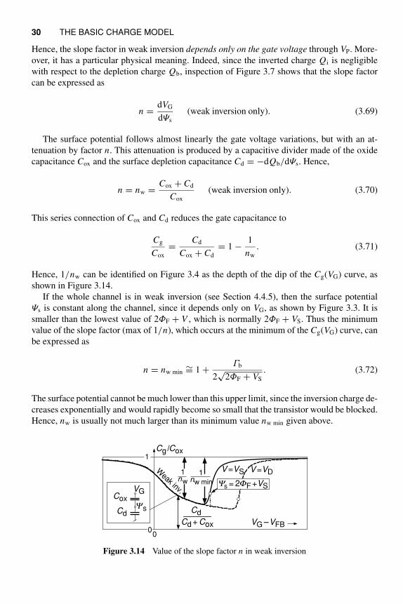
30 THE BASIC CHARGE MODEL
Hence, the slope factor in weak inversion depends only on the gate voltage through VP. More-
over, it has a particular physical meaning. Indeed, since the inverted charge Qi is negligible
with respect to the depletion charge Qb, inspection of Figure 3.7 shows that the slope factor
can be expressed as
n =dVG
dΨs
(weak inversion only). (3.69)
The surface potential follows almost linearly the gate voltage variations, but with an at-
tenuation by factor n. This attenuation is produced by a capacitive divider made of the oxide
capacitance Cox and the surface depletion capacitance Cd = −dQb/dΨs. Hence,
n = nw =Cox + Cd
Cox
(weak inversion only). (3.70)
This series connection of Cox and Cd reduces the gate capacitance to
Cg
Cox
=Cd
Cox + Cd
= 1 −1
nw
. (3.71)
Hence, 1/nw can be identified on Figure 3.4 as the depth of the dip of the Cg(VG) curve, as
shown in Figure 3.14.
If the whole channel is in weak inversion (see Section 4.4.5), then the surface potential
Ψs is constant along the channel, since it depends only on VG, as shown by Figure 3.3. It is
smaller than the lowest value of 2ΦF + V , which is normally 2ΦF + VS. Thus the minimum
value of the slope factor (max of 1/n), which occurs at the minimum of the Cg(VG) curve, can
be expressed as
n = nw min∼= 1 +
Γb
2√
2ΦF + VS
. (3.72)
The surface potential cannot be much lower than this upper limit, since the inversion charge de-
creases exponentially and would rapidly become so small that the transistor would be blocked.
Hence, nw is usually not much larger than its minimum value nw min given above.
VG
Ys
Cox
Cd
0
VG –VFB
Cg /Cox
V =VS V =VD
Cd
Cd + Cox0
Weak inv.
1
1nw
1nw min Ys = 2FF +VS
Figure 3.14 Value of the slope factor n in weak inversion
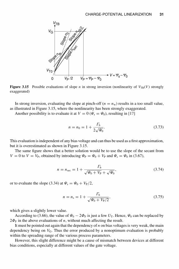
CHARGE-POTENTIAL LINEARIZATION 31
VG
VP = YP – Y0
V = Ys – Y0
VT0
VP /20
Slope
n w
Slo
pe n
0Slo
pe n vp
/2
Slo
pe n se
c
VTB
Figure 3.15 Possible evaluations of slope n in strong inversion (nonlinearity of VTB(V ) strongly
exaggerated)
In strong inversion, evaluating the slope at pinch-off (n = nw) results in a too small value,
as illustrated in Figure 3.15, where the nonlinearity has been strongly exaggerated.
Another possibility is to evaluate it at V = 0 (Ψs = Ψ0), resulting in [17]
n = n0 = 1 +Γb
2√
Ψ0
. (3.73)
This evaluation is independent of any bias voltage and can thus be used as a first approximation,
but it is overestimated as shown in Figure 3.15.
The same figure shows that a better solution would be to use the slope of the secant from
V = 0 to V = VP, obtained by introducing ΨP = Ψ0 + VP and Ψs = Ψ0 in (3.67),
n = nsec = 1 +Γb√
Ψ0 + VP +√
Ψ0
, (3.74)
or to evaluate the slope (3.34) at Ψs = Ψ0 + VP/2,
n = ns = 1 +Γb√
Ψ0 + VP/2, (3.75)
which gives a slightly lower value.
According to (3.66), the value of Ψ0 − 2ΦF is just a few UT. Hence, Ψ0 can be replaced by
2ΦF in the above evaluations of n, without much affecting the result.
It must be pointed out again that the dependency of n on bias voltages is very weak, the main
dependency being on VG. Thus the error produced by a nonoptimum evaluation is probably
within the spreading range of the various process parameters.
However, this slight difference might be a cause of mismatch between devices at different
bias conditions, especially at different values of the gate voltage.
32 THE BASIC CHARGE MODEL
3.6.5 Compact Model Parameters
Equation (3.48) describes the general charge–voltage relationship for a long-channel transistor.
This equation is dimensionless and uses normalized variables. Only three model parameters
and one physical parameter are needed to obtain from it the relation between applied voltages
VG and V , and the resulting inverted charge density Qi.
The physical parameter, used to normalize all voltages in the dimensionless equation is UT.
The following are the three device parameters:
1. The slope factor n defined in Figure 3.7 and by equation (3.34). This parameter was further
discussed in Section 3.6.4.
2. The threshold voltage VT0 defined in Figure 3.12 and by equations (3.58) and (3.66). It is
very slightly dependent on VG through Ψp (see Figure 3.10), but can be considered bias
independent in practice.
These first two parameters relate the gate voltage VG to the pinch-off voltage VP according
to (3.63).
3. The oxide capacitance per unit area Cox. It is combined with n and UT to obtain the specific
charge Qspec defined by (3.42) and is used to normalize the charge density.
Introducing these parameters in (3.48) provides the nonnormalized general charge–voltage
relation:
−Qi
Cox
+ nUT ln−Qi
2nCoxUT
= VG − VT0 − nV . (3.76)
We can see that UT plays an important role in weak inversion where the logarithmic term
dominates. This role disappears in strong inversion when the logarithmic term becomes neg-
ligible.

4 Static Drain Current
In this chapter, the model of the static current–voltage characteristics of the transistor is derived.
In Section 4.1, the drain current ID is shown to be directly related to the charge–voltage relation
established in the previous chapter. Section 4.2 introduces the important concept of forward
and reverse components of ID, and Section 4.3 defines the various modes of operation of the
transistor. Section 4.4 details the derivation of the drain current for all current levels from the
linearized charge model, with its approximations in strong and weak inversion. Section 4.5 is
dedicated to a fundamental property of the transistor that facilitates its modeling and opens
interesting circuit approaches through the concept of pseudo-resistor. Finally, Section 4.6
introduces a first approximation of the channel length modulation phenomenon, which limits
the output resistance in saturation.
4.1 DRAIN CURRENT EXPRESSION
When the source and drain voltages are different, electrons of density np forming the mobile
inverted charge Qi move by a combination of drift and diffusion, resulting in a drain current
ID defined in Figure 2.1. For the long channel considered here, all elementary flows of current
are along the x-axis with a local current density in this direction given by [67]
Jn = μq
⎛
⎜⎜⎝
−np
dΨ
dx︸ ︷︷ ︸
drift
+ UT
dnp
dx︸ ︷︷ ︸
diffusion
⎞
⎟⎟⎠
, (4.1)
where µ is the equivalent mobility of electrons in the channel. The first term is the drift
component of the current, proportional to the longitudinal electric field −dΨ/dx . The second
term is the diffusion component, proportional to the gradient of charge concentration dnp/dx .
With the charge sheet approximation, integration in the vertical direction (z-axis) is obtained
by replacing qnp by −Qi. Moreover, if the channel is sufficiently wide, integration along the
Charge-Based MOS Transistor Modeling: The EKV Model for Low-Power and RF IC Design C. Enz and E. VittozC© 2006 John Wiley & Sons, Ltd.
34 STATIC DRAIN CURRENT
y-axis is simply a multiplication by width W . Thus [1],
ID = μW
⎛
⎜⎜⎝
−Qi
dΨs
dx︸ ︷︷ ︸
drift
+ UT
dQi
dx︸ ︷︷ ︸
diffusion
⎞
⎟⎟⎠
, (4.2)
Since the whole charge Qi of electrons is assumed to be concentrated at the surface, the
concentration of electrons (3.5) can be replaced by
Qi ∝ expΨs − ΦF − V
UT
. (4.3)
Therefore
dQi
dx=
Qi
UT
(dΨs
dx−
dV
dx
)
, (4.4)
which when introduced in (4.2) yields
ID = μW (−Qi)dV
dx. (4.5)
This expression includes the drift and the diffusion components and shows that the overall
current is proportional to the gradient of channel voltage V (which is a quasi-Fermi potential,
as discussed in Section 2.1). Now, since the current is constant along the channel, (4.5) can be
integrated from source to drain:
ID
∫ L
0
dx =∫ VD
VS
μW (−Qi)dV . (4.6)
In this basic model, mobility μ and channel width W are assumed to be constant. The depen-
dency of μ on the vertical field Ezs and the horizontal field Ex will be introduced in Part II.
The effect of a possible variable channel width will be discussed in Section 4.5.2. Since only
Qi changes along the channel, equation (4.6) becomes
ID = β
∫ VD
VS
−Qi
Cox
dV, (4.7)
where
β μCox
W
L(4.8)
is the transfer parameter of the transistor depending on the width over length ratio of the
channel.
Equation (4.7) is a very interesting result, since it shows that the drain current can be
obtained directly from the Qi(V ) as is illustrated in Figure 4.1. This result is independent of
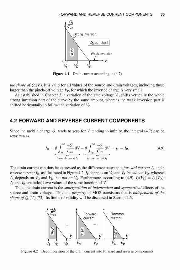
FORWARD AND REVERSE CURRENT COMPONENTS 35
IDb
V
VP
–Q iCox
VS VD
0
Strong inversion:
Weak inversion
VG constant
Figure 4.1 Drain current according to (4.7)
the shape of Qi(V ). It is valid for all values of the source and drain voltages, including those
larger than the pinch-off voltage VP, for which the inverted charge is very small.
As established in Chapter 3, a variation of the gate voltage VG shifts vertically the whole
strong inversion part of the curve by the same amount, whereas the weak inversion part is
shifted horizontally to follow the variation of VP.
4.2 FORWARD AND REVERSE CURRENT COMPONENTS
Since the mobile charge Qi tends to zero for V tending to infinity, the integral (4.7) can be
rewritten as
ID = β
∫ ∞
VS
−Qi
Cox
dV
︸ ︷︷ ︸
forward current IF
− β
∫ ∞
VD
−Qi
Cox
dV
︸ ︷︷ ︸
reverse current IR
= IF − IR. (4.9)
The drain current can thus be expressed as the difference between a forward current IF and a
reverse current IR, as illustrated in Figure 4.2. IF depends on VG and VS, but not on VD, whereas
IR depends on VG and VD, but not on VS. Furthermore, according to (4.9), IF(VS) ≡ IR(VD):
IF and IR are indeed two values of the same function of V.
Thus, the drain current is the superposition of independent and symmetrical effects of the
source and drain voltages. This is a property of MOS transistors that is independent of the
shape of Qi(V ) [73]. Its limits of validity will be discussed in Section 4.5.
IDb
V
VP
–Q iCox
VS VD
=
V
VPVS
IFb
V
VPVD
IRb
Forwardcurrent
Reversecurrent
Figure 4.2 Decomposition of the drain current into forward and reverse components
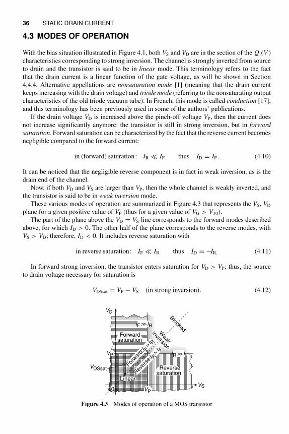
36 STATIC DRAIN CURRENT
4.3 MODES OF OPERATION
With the bias situation illustrated in Figure 4.1, both VS and VD are in the section of the Qi(V )
characteristics corresponding to strong inversion. The channel is strongly inverted from source
to drain and the transistor is said to be in linear mode. This terminology refers to the fact
that the drain current is a linear function of the gate voltage, as will be shown in Section
4.4.4. Alternative appellations are nonsaturation mode [1] (meaning that the drain current
keeps increasing with the drain voltage) and triode mode (referring to the nonsaturating output
characteristics of the old triode vacuum tube). In French, this mode is called conduction [17],
and this terminology has been previously used in some of the authors’ publications.
If the drain voltage VD is increased above the pinch-off voltage VP, then the current does
not increase significantly anymore: the transistor is still in strong inversion, but in forward
saturation. Forward saturation can be characterized by the fact that the reverse current becomes
negligible compared to the forward current:
in (forward) saturation : IR ≪ IF thus ID = IF. (4.10)
It can be noticed that the negligible reverse component is in fact in weak inversion, as is the
drain end of the channel.
Now, if both VD and VS are larger than VP, then the whole channel is weakly inverted, and
the transistor is said to be in weak inversion mode.
These various modes of operation are summarized in Figure 4.3 that represents the VS, VD
plane for a given positive value of VP (thus for a given value of VG > VT0).
The part of the plane above the VD = VS line corresponds to the forward modes described
above, for which ID > 0. The other half of the plane corresponds to the reverse modes, with
VS > VD; therefore, ID < 0. It includes reverse saturation with
in reverse saturation : IF ≪ IR thus ID = −IR. (4.11)
In forward strong inversion, the transistor enters saturation for VD > VP; thus, the source
to drain voltage necessary for saturation is
VDSsat = VP − VS (in strong inversion). (4.12)
VS
VD
Forwardsaturation
Reversesaturation
Weak
inversion
Blocked
IR >>IF
IF >>IR
0 VP
VP
VDSsat
Linear
Forwar
d: I F
>I R
Rev
erse
: I R>I F
Figure 4.3 Modes of operation of a MOS transistor
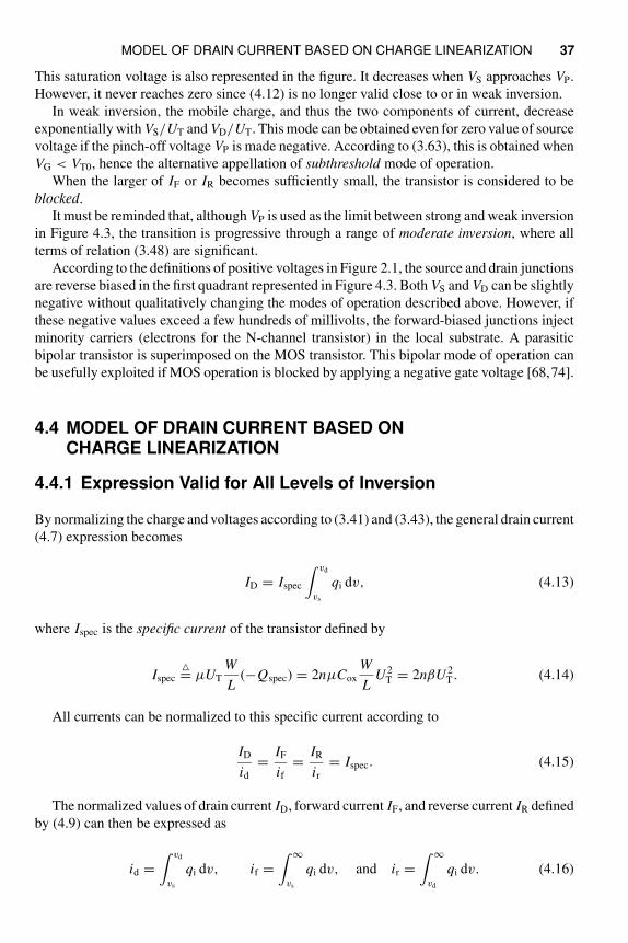
MODEL OF DRAIN CURRENT BASED ON CHARGE LINEARIZATION 37
This saturation voltage is also represented in the figure. It decreases when VS approaches VP.
However, it never reaches zero since (4.12) is no longer valid close to or in weak inversion.
In weak inversion, the mobile charge, and thus the two components of current, decrease
exponentially with VS/UT and VD/UT. This mode can be obtained even for zero value of source
voltage if the pinch-off voltage VP is made negative. According to (3.63), this is obtained when
VG < VT0, hence the alternative appellation of subthreshold mode of operation.
When the larger of IF or IR becomes sufficiently small, the transistor is considered to be
blocked.
It must be reminded that, although VP is used as the limit between strong and weak inversion
in Figure 4.3, the transition is progressive through a range of moderate inversion, where all
terms of relation (3.48) are significant.
According to the definitions of positive voltages in Figure 2.1, the source and drain junctions
are reverse biased in the first quadrant represented in Figure 4.3. Both VS and VD can be slightly
negative without qualitatively changing the modes of operation described above. However, if
these negative values exceed a few hundreds of millivolts, the forward-biased junctions inject
minority carriers (electrons for the N-channel transistor) in the local substrate. A parasitic
bipolar transistor is superimposed on the MOS transistor. This bipolar mode of operation can
be usefully exploited if MOS operation is blocked by applying a negative gate voltage [68,74].
4.4 MODEL OF DRAIN CURRENT BASED ONCHARGE LINEARIZATION
4.4.1 Expression Valid for All Levels of Inversion
By normalizing the charge and voltages according to (3.41) and (3.43), the general drain current
(4.7) expression becomes
ID = Ispec
∫ vd
vs
qi dv, (4.13)
where Ispec is the specific current of the transistor defined by
Ispec= μUT
W
L(−Qspec) = 2nμCox
W
LU 2
T = 2nβU 2T. (4.14)
All currents can be normalized to this specific current according to
ID
id
=IF
if
=IR
ir
= Ispec. (4.15)
The normalized values of drain current ID, forward current IF, and reverse current IR defined
by (4.9) can then be expressed as
id =∫ vd
vs
qi dv, if =∫ ∞
vs
qi dv, and ir =∫ ∞
vd
qi dv. (4.16)
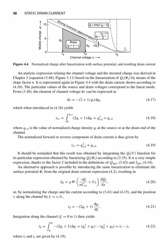
38 STATIC DRAIN CURRENT
Areaid = if – ir
qi =vp–v
2
∆qi
qi = exp( vp– v)
Channel voltage v
Mo
bile
ch
arg
e
Strong inversion approximation
1
10
0
5
vpvs vd
qs
qd
qi
Figure 4.4 Normalized charge after linearization with surface potential, and resulting drain current
An analytic expression relating the channel voltage and the inverted charge was derived in
Chapter 3 (equation (3.48); Figure 3.11) based on the linearization of Qi(Ψs) by means of the
slope factor n. It is represented again in Figure 4.4 with the drain current shown according to
(4.16). The particular values of the source and drain voltages correspond to the linear mode.
From (3.48), the element of channel voltage dv can be expressed as
dv = −(2 + 1/qi) dqi, (4.17)
which when introduced in (4.16) yields
if,r =∫ qs,d
0
(2qi + 1) dqi = q2s,d + qs,d (4.18)
where qs,d is the value of normalized charge density qi at the source or at the drain end of the
channel.
The normalized forward or reverse component of drain current is thus given by
if,r = q2s,d + qs,d. (4.19)
It should be reminded that this result was obtained by integrating the Qi(V ) function for
its particular expression obtained by linearizing Qi(Ψs) according to (3.35). It is a very simple
expression, thanks to the factor 2 included in the definitions of Qspec (3.42) and Ispec (4.14).
An alternative approach is possible by introducing the same linearization to eliminate the
surface potential Ψs from the original drain current expression (4.2), resulting in
ID = µW
(−Qi
nCox
+ UT
)dQi
dx, (4.20)
or, by normalizing the charge and the current according to (3.41) and (4.15), and the position
x along the channel by ξ = x/L ,
id = −(2qi + 1)dqi
dξ. (4.21)
Integration along the channel (ξ = 0 to 1) then yields
id =∫ qd
qs
−(2qi + 1) dqi = (q2s + qs) − (q2
d + qd) = if − ir. (4.22)
where if and ir are given by (4.19).
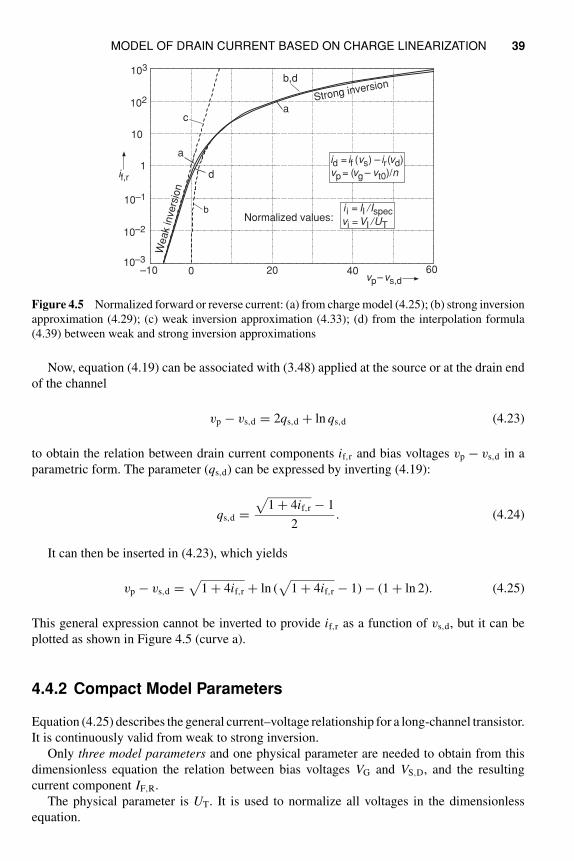
MODEL OF DRAIN CURRENT BASED ON CHARGE LINEARIZATION 39
0 20 40
102
10–2
1
vp–vs,d
if,r
a
b,d
b
c
id = if (vs) – ir (vd)
vp= (vg – vt0)/n
i i = II /Ispecvi =VI /UT
Normalized values:
Strong inversion
–10
Weak
inve
rsio
n
10
10–3
103
10–1
60
a
d
Figure 4.5 Normalized forward or reverse current: (a) from charge model (4.25); (b) strong inversion
approximation (4.29); (c) weak inversion approximation (4.33); (d) from the interpolation formula
(4.39) between weak and strong inversion approximations
Now, equation (4.19) can be associated with (3.48) applied at the source or at the drain end
of the channel
vp − vs,d = 2qs,d + ln qs,d (4.23)
to obtain the relation between drain current components if,r and bias voltages vp − vs,d in a
parametric form. The parameter (qs,d) can be expressed by inverting (4.19):
qs,d =√
1 + 4if,r − 1
2. (4.24)
It can then be inserted in (4.23), which yields
vp − vs,d =√
1 + 4if,r + ln (√
1 + 4if,r − 1) − (1 + ln 2). (4.25)
This general expression cannot be inverted to provide if,r as a function of vs,d, but it can be
plotted as shown in Figure 4.5 (curve a).
4.4.2 Compact Model Parameters
Equation (4.25) describes the general current–voltage relationship for a long-channel transistor.
It is continuously valid from weak to strong inversion.
Only three model parameters and one physical parameter are needed to obtain from this
dimensionless equation the relation between bias voltages VG and VS,D, and the resulting
current component IF,R.
The physical parameter is UT. It is used to normalize all voltages in the dimensionless
equation.
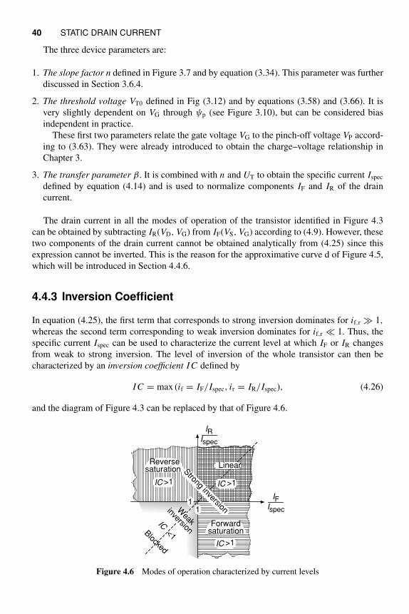
40 STATIC DRAIN CURRENT
The three device parameters are:
1. The slope factor n defined in Figure 3.7 and by equation (3.34). This parameter was further
discussed in Section 3.6.4.
2. The threshold voltage VT0 defined in Fig (3.12) and by equations (3.58) and (3.66). It is
very slightly dependent on VG through ψp (see Figure 3.10), but can be considered bias
independent in practice.
These first two parameters relate the gate voltage VG to the pinch-off voltage VP accord-
ing to (3.63). They were already introduced to obtain the charge–voltage relationship in
Chapter 3.
3. The transfer parameter β. It is combined with n and UT to obtain the specific current Ispec
defined by equation (4.14) and is used to normalize components IF and IR of the drain
current.
The drain current in all the modes of operation of the transistor identified in Figure 4.3
can be obtained by subtracting IR(VD, VG) from IF(VS, VG) according to (4.9). However, these
two components of the drain current cannot be obtained analytically from (4.25) since this
expression cannot be inverted. This is the reason for the approximative curve d of Figure 4.5,
which will be introduced in Section 4.4.6.
4.4.3 Inversion Coefficient
In equation (4.25), the first term that corresponds to strong inversion dominates for if,r ≫ 1,
whereas the second term corresponding to weak inversion dominates for if,r ≪ 1. Thus, the
specific current Ispec can be used to characterize the current level at which IF or IR changes
from weak to strong inversion. The level of inversion of the whole transistor can then be
characterized by an inversion coefficient I C defined by
I C = max (if = IF/Ispec, ir = IR/Ispec), (4.26)
and the diagram of Figure 4.3 can be replaced by that of Figure 4.6.
Linear
Forwardsaturation
Reversesaturation
Blocked
IFIspec
IRIspec
11
IC <1
IC >1
IC >1
IC >1
Strong inversionWeak
inversion
Figure 4.6 Modes of operation characterized by current levels
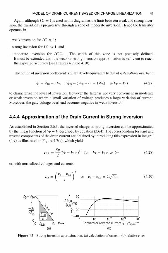
MODEL OF DRAIN CURRENT BASED ON CHARGE LINEARIZATION 41
Again, although I C = 1 is used in this diagram as the limit between weak and strong inver-
sion, the transition is progressive through a zone of moderate inversion. Hence the transistor
operates in
– weak inversion for I C ≪ 1;
– strong inversion for I C ≫ 1; and
– moderate inversion for I C ∼= 1. The width of this zone is not precisely defined.
It must be extended until the weak or strong inversion approximation is sufficient to reach
the expected accuracy (see Figures 4.7 and 4.10).
The notion of inversion coefficient is qualitatively equivalent to that of gate voltage overhead
VG − VT0 − nVS = VGS − (VT0 + (n − 1)VS) = n(VP − VS) (4.27)
to characterize the level of inversion. However the latter is not very convenient in moderate
or weak inversion where a small variation of voltage produces a large variation of current.
Moreover, the gate voltage overhead becomes negative in weak inversion.
4.4.4 Approximation of the Drain Current in Strong Inversion
As established in Section 3.6.3, the inverted charge in strong inversion can be approximated
by the linear function of VP − V described by equation (3.64). The corresponding forward and
reverse components of the drain current are obtained by introducing this expression in integral
(4.9) as illustrated in Figure 4.7(a), which yields
IF,R =βn
2(VP − VS,D)2 for VP − VS,D ≫ UT (4.28)
or, with normalized voltages and currents
if,r =(
vp − vs,d
2
)2
or vp − vs,d = 2√
if,r. (4.29)
VS,D VP00
VG –VT0
Slope –
nIF,Rb
V
(a)
–Q iCox
–40
–20
20
0
1 10 102 103 104
∆IF,RIF,R
(%)
Err
or
Forward or reverse current IF,R/Ispec
(b)
Figure 4.7 Strong inversion approximation: (a) calculation of current; (b) relative error
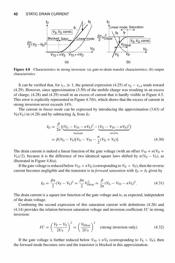
42 STATIC DRAIN CURRENT
VG
VT0 + nVS VT0 + nVD
IRID
(VD –VS)2bn2
IF
Blocked Linear modeSatur.
VS,VD const.
(a)
bn2
VDSsat2
VS VP
VD
VDSsat
IR
ID
Linear mode Saturation
IF
VS,VG const.
(b)
Figure 4.8 Characteristics in strong inversion: (a) gate-to-drain transfer characteristics; (b) output
characteristics
It can be verified that, for if,r ≫ 1, the general expression (4.25) of vp − vs,d tends toward
(4.29). However, since approximation (3.50) of the mobile charge was resulting in an excess
of charge, (4.28) and (4.29) result in an excess of current that is hardly visible in Figure 4.5.
This error is explicitly represented in Figure 4.7(b), which shows that the excess of current in
strong inversion never exceeds 14%.
The current in linear mode can be expressed by introducing the approximation (3.63) of
VP(VG) in (4.28) and by subtracting IR from IF:
ID =β
2n[(VG − VT0 − nVS)2
︸ ︷︷ ︸
forward
− (VG − VT0 − nVD)2
︸ ︷︷ ︸
reverse
]
= β(VD − VS)[VG − VT0 −n
2(VD + VS)]. (4.30)
The drain current is indeed a linear function of the gate voltage (with an offset VT0 + n(VD +VS)/2), because it is the difference of two identical square laws shifted by n(VD − VS), as
illustrated in Figure 4.8(a).
If the gate voltage is reduced below VT0 + nVD (corresponding to VD > VP), then the reverse
current becomes negligible and the transistor is in forward saturation with ID = IF given by
ID =βn
2(VP − VS)2 =
βn
2V 2
DSsat =β
2n(VG − VT0 − nVS)2. (4.31)
The drain current is a square law function of the gate voltage and is, as expected, independent
of the drain voltage.
Combining the second expression of this saturation current with definitions (4.26) and
(4.14) provides the relation between saturation voltage and inversion coefficient I C in strong
inversion:
I C =(
VP − VS
2UT
)2
=(
VDSsat
2UT
)2
(strong inversion only). (4.32)
If the gate voltage is further reduced below VT0 + nVS (corresponding to VS > VP), then
the forward mode becomes zero and the transistor is blocked in this approximation.
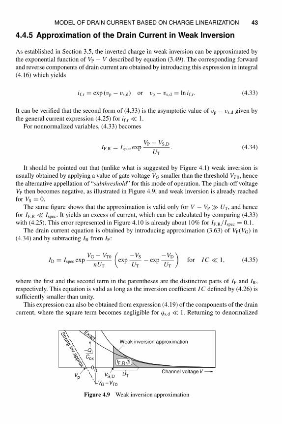
MODEL OF DRAIN CURRENT BASED ON CHARGE LINEARIZATION 43
4.4.5 Approximation of the Drain Current in Weak Inversion
As established in Section 3.5, the inverted charge in weak inversion can be approximated by
the exponential function of VP − V described by equation (3.49). The corresponding forward
and reverse components of drain current are obtained by introducing this expression in integral
(4.16) which yields
if,r = exp (vp − vs,d) or vp − vs,d = ln if,r. (4.33)
It can be verified that the second form of (4.33) is the asymptotic value of vp − vs,d given by
the general current expression (4.25) for if,r ≪ 1.
For nonnormalized variables, (4.33) becomes
IF,R = Ispec expVP − VS,D
UT
. (4.34)
It should be pointed out that (unlike what is suggested by Figure 4.1) weak inversion is
usually obtained by applying a value of gate voltage VG smaller than the threshold VT 0, hence
the alternative appellation of “subthreshold” for this mode of operation. The pinch-off voltage
VP then becomes negative, as illustrated in Figure 4.9, and weak inversion is already reached
for VS = 0.
The same figure shows that the approximation is valid only for V − VP ≫ UT, and hence
for IF,R ≪ Ispec. It yields an excess of current, which can be calculated by comparing (4.33)
with (4.25). This error represented in Figure 4.10 is already about 10% for IF,R/Ispec = 0.1.
The drain current equation is obtained by introducing approximation (3.63) of VP(VG) in
(4.34) and by subtracting IR from IF:
ID = Ispec expVG − VT0
nUT
(
exp−VS
UT
− exp−VD
UT
)
for I C ≪ 1, (4.35)
where the first and the second term in the parentheses are the distinctive parts of IF and IR,
respectively. This equation is valid as long as the inversion coefficient I C defined by (4.26) is
sufficiently smaller than unity.
This expression can also be obtained from expression (4.19) of the components of the drain
current, where the square term becomes negligible for qs,d ≪ 1. Returning to denormalized
Vp
VG –VT0
0
Strong inv.approx
ExactWeak inversion approximation
–Q iCox
0Channel voltage V
VS,D
IF,R /b
UT
Figure 4.9 Weak inversion approximation
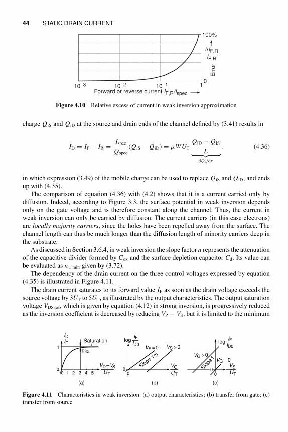
44 STATIC DRAIN CURRENT
0
100%
10–3 110–2 10–1
Forward or reverse current IF,R/Ispec
∆IF,RIF,R
Err
or
Figure 4.10 Relative excess of current in weak inversion approximation
charge QiS and QiD at the source and drain ends of the channel defined by (3.41) results in
ID = IF − IR =Ispec
Qspec
(QiS − QiD) = μWUT
QiD − QiS
L︸ ︷︷ ︸
dQi/dx
. (4.36)
in which expression (3.49) of the mobile charge can be used to replace QiS and QiD, and ends
up with (4.35).
The comparison of equation (4.36) with (4.2) shows that it is a current carried only by
diffusion. Indeed, according to Figure 3.3, the surface potential in weak inversion depends
only on the gate voltage and is therefore constant along the channel. Thus, the current in
weak inversion can only be carried by diffusion. The current carriers (in this case electrons)
are locally majority carriers, since the holes have been repelled away from the surface. The
channel length can thus be much longer than the diffusion length of minority carriers deep in
the substrate.
As discussed in Section 3.6.4, in weak inversion the slope factor n represents the attenuation
of the capacitive divider formed by Cox and the surface depletion capacitor Cd. Its value can
be evaluated as nw min given by (3.72).
The dependency of the drain current on the three control voltages expressed by equation
(4.35) is illustrated in Figure 4.11.
The drain current saturates to its forward value IF as soon as the drain voltage exceeds the
source voltage by 3UT to 5UT, as illustrated by the output characteristics. The output saturation
voltage VDS sat, which is given by equation (4.12) in strong inversion, is progressively reduced
as the inversion coefficient is decreased by reducing VP − VS, but it is limited to the minimum
Slope
1
logIF
ID0
VS
UT–
00
VG = 0VG >0
(c)
logIF
ID0
Slope 1/n
VS =0 VS > 0
VG
UT0
0
(b)
1
0
5%
VD –VS
UT
IDIF Saturation
0 31 2 4 5
(a)
Figure 4.11 Characteristics in weak inversion: (a) output characteristics; (b) transfer from gate; (c)
transfer from source
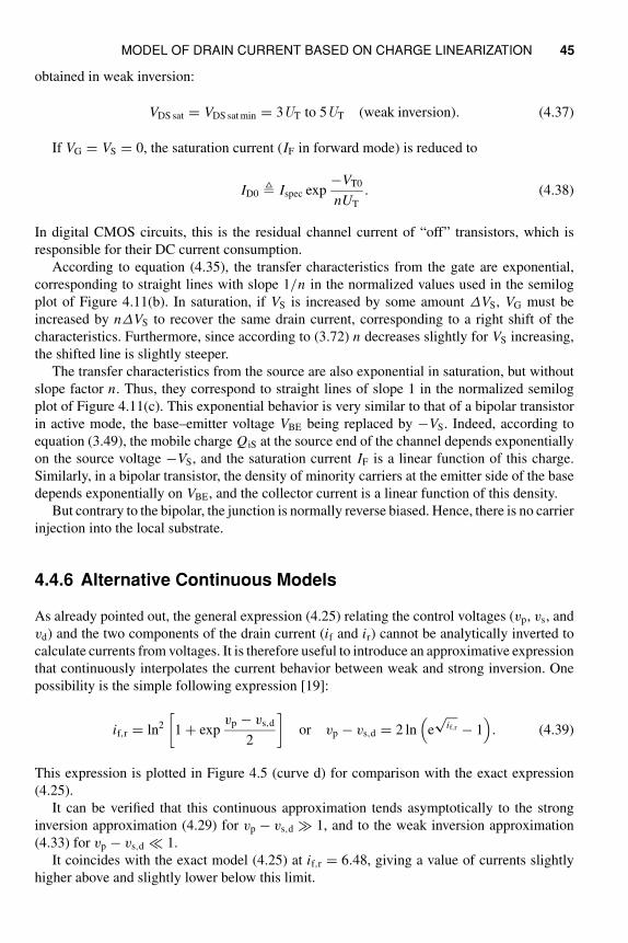
MODEL OF DRAIN CURRENT BASED ON CHARGE LINEARIZATION 45
obtained in weak inversion:
VDS sat = VDS sat min = 3UT to 5UT (weak inversion). (4.37)
If VG = VS = 0, the saturation current (IF in forward mode) is reduced to
ID0 Ispec exp−VT0
nUT
. (4.38)
In digital CMOS circuits, this is the residual channel current of “off” transistors, which is
responsible for their DC current consumption.
According to equation (4.35), the transfer characteristics from the gate are exponential,
corresponding to straight lines with slope 1/n in the normalized values used in the semilog
plot of Figure 4.11(b). In saturation, if VS is increased by some amount ΔVS, VG must be
increased by nΔVS to recover the same drain current, corresponding to a right shift of the
characteristics. Furthermore, since according to (3.72) n decreases slightly for VS increasing,
the shifted line is slightly steeper.
The transfer characteristics from the source are also exponential in saturation, but without
slope factor n. Thus, they correspond to straight lines of slope 1 in the normalized semilog
plot of Figure 4.11(c). This exponential behavior is very similar to that of a bipolar transistor
in active mode, the base–emitter voltage VBE being replaced by −VS. Indeed, according to
equation (3.49), the mobile charge QiS at the source end of the channel depends exponentially
on the source voltage −VS, and the saturation current IF is a linear function of this charge.
Similarly, in a bipolar transistor, the density of minority carriers at the emitter side of the base
depends exponentially on VBE, and the collector current is a linear function of this density.
But contrary to the bipolar, the junction is normally reverse biased. Hence, there is no carrier
injection into the local substrate.
4.4.6 Alternative Continuous Models
As already pointed out, the general expression (4.25) relating the control voltages (vp, vs, and
vd) and the two components of the drain current (if and ir) cannot be analytically inverted to
calculate currents from voltages. It is therefore useful to introduce an approximative expression
that continuously interpolates the current behavior between weak and strong inversion. One
possibility is the simple following expression [19]:
if,r = ln2
[
1 + expvp − vs,d
2
]
or vp − vs,d = 2 ln(
e√
if,r − 1)
. (4.39)
This expression is plotted in Figure 4.5 (curve d) for comparison with the exact expression
(4.25).
It can be verified that this continuous approximation tends asymptotically to the strong
inversion approximation (4.29) for vp − vs,d ≫ 1, and to the weak inversion approximation
(4.33) for vp − vs,d ≪ 1.
It coincides with the exact model (4.25) at if,r = 6.48, giving a value of currents slightly
higher above and slightly lower below this limit.
46 STATIC DRAIN CURRENT
4.5 FUNDAMENTAL PROPERTY: VALIDITYAND APPLICATION
4.5.1 Generalization of Drain Current Expression
The fundamental property of long-channel MOS transistor obtained in Section 4.2 can be
generalized [73] if equation (4.5) of the drain current can be written in the form
ID =FV(V, VG)
Fx(x, VG)
dV
dx(4.40)
where FV(V, VG) is a function of V and VG but not of x , and Fx(x, VG) is a function of x and
VG but not of V ; ID is then a separable function of position x and voltage V in the channel. As
long as the channel length L is independent of VD and VS, Fx(x, VG) and FV(V, VG) can then
be integrated separately:
ID
∫ L
0
Fx(x, VG) dx =∫ VD
VS
FV(V, VG) dV . (4.41)
Now, since FV(V, VG) tends to zero for large V , this expression can be written as
ID =1
∫ L
0Fx(x, VG) dx
[∫ ∞
VS
FV(V, VG) dV −∫ ∞
VD
FV(V, VG) dV
]
(4.42)
or
ID = I (VS, VG) − I (VD, VG) = IF − IR, (4.43)
where
I (V, VG) =∫ ∞
VFV(V, VG) dV
∫ L
0Fx(x, VG) dx
. (4.44)
This result is a generalization of (4.9), expressing the fact that the drain current is the
superposition of independent and symmetrical (same function I ) effects of source and drain
voltages.
It is interesting to point out that this property is similar to that of bipolar transistors as
expressed by the Ebers–Moll model [18].
4.5.2 Domain of Validity
Let us examine the necessary and sufficient conditions for which equation (4.5) has the required
form (4.40).
The channel width W does not depend on V. It may thus depend on position x along the
channel, and therefore can be included in Fx(x, VG). For example, in a concentric circular
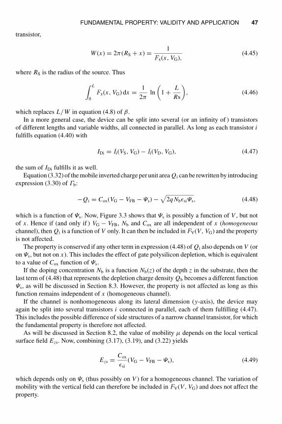
FUNDAMENTAL PROPERTY: VALIDITY AND APPLICATION 47
transistor,
W (x) = 2π (RS + x) =1
Fx(x, VG),(4.45)
where RS is the radius of the source. Thus
∫ L
0
Fx(x, VG) dx =1
2πln
(
1 +L
Rs
)
, (4.46)
which replaces L/W in equation (4.8) of β.
In a more general case, the device can be split into several (or an infinity of ) transistors
of different lengths and variable widths, all connected in parallel. As long as each transistor i
fulfills equation (4.40) with
IDi = Ii(VS, VG) − Ii(VD, VG), (4.47)
the sum of IDi fulfills it as well.
Equation (3.32) of the mobile inverted charge per unit area Qi can be rewritten by introducing
expression (3.30) of Γb:
−Qi = Cox(VG − VFB − Ψs) −√
2q NbǫsiΨs, (4.48)
which is a function of Ψs. Now, Figure 3.3 shows that Ψs is possibly a function of V , but not
of x . Hence if (and only if ) VG − VFB, Nb and Cox are all independent of x (homogeneous
channel), then Qi is a function of V only. It can then be included in FV(V, VG) and the property
is not affected.
The property is conserved if any other term in expression (4.48) of Qi also depends on V (or
on Ψs, but not on x). This includes the effect of gate polysilicon depletion, which is equivalent
to a value of Cox function of Ψs.
If the doping concentration Nb is a function Nb(z) of the depth z in the substrate, then the
last term of (4.48) that represents the depletion charge density Qb becomes a different function
Ψs, as will be discussed in Section 8.3. However, the property is not affected as long as this
function remains independent of x (homogeneous channel).
If the channel is nonhomogeneous along its lateral dimension (y-axis), the device may
again be split into several transistors i connected in parallel, each of them fulfilling (4.47).
This includes the possible difference of side structures of a narrow channel transistor, for which
the fundamental property is therefore not affected.
As will be discussed in Section 8.2, the value of mobility μ depends on the local vertical
surface field Ezs. Now, combining (3.17), (3.19), and (3.22) yields
Ezs =Cox
ǫsi
(VG − VFB − Ψs), (4.49)
which depends only on Ψs (thus possibly on V ) for a homogeneous channel. The variation of
mobility with the vertical field can therefore be included in FV(V, VG) and does not affect the
property.
48 STATIC DRAIN CURRENT
But the mobility should be independent of the drain current ID. Indeed, such a dependency
could be included neither in FV(V, VG) nor in Fx(x, VG), hence, the property would not be
conserved.
As another necessary condition, the effective value of the channel length L along which
Fx(x, VG) is integrated in (4.41) should be constant. It should not depend on the drain current
ID, or on the drain or source voltage VD or VS.
In summary, the fundamental property of MOS transistors expressed by equation (4.40) is
valid if (and only if ) the channel is homogeneous along its source–drain dimension (x-axis)
with a fixed effective length, and if (and only if) the mobility is independent of the drain current.
The property depends neither on the shape and width of the channel nor on the doping profile
of the substrate. It remains valid for large gate voltages, in spite of the mobility reduction due
to the vertical field.
4.5.3 Causes of Degradation
4.5.3.1 Finite length of channel
When the channel is not very long, several independent mechanisms degrade the fundamental
property. This is the most important reason why this property is never perfectly valid in practice.
Channel length modulation. As will be discussed in Section 4.6, when the drain (or source)
voltage is increased, the effective channel length is slightly reduced by the extension of the
depleted region surrounding the drain (or the source). As expressed by (4.59) or (4.61), the
forward current IF (or reverse current IR) is therefore slightly dependent on the drain voltage
VD (or the source voltage VS), which is not compatible with (4.43). Since this effect is inversely
proportional to L , the property is progressively degraded when the channel is shortened.
Short-channel effects. If the channel length is reduced more than proportionally to the gate
and drain voltages, the longitudinal field in the channel is increased. Hence, the velocity of
mobile carriers is increased, resulting in an increase of drain current. However, at high values,
this velocity starts increasing less than proportionally to the field, to finally reach a saturation
limit. Thus, mobility μ becomes a function of the field (or of the current), as will be discussed
in Section 9.1.
This variation cannot be included in Fx(x, VG) or FV(V, VG) as required by (4.40), and the
property is degraded.
For very short channel, additional effects such as drain-induced barrier lowering discussed
in Section 9.3 and other two-dimensional effects further degrade and possibly destroy the
property.
4.5.3.2 Nonhomogeneous channel
Referring to equation (4.48), if any term of its right-hand side depends on position x along
the channel, it makes Qi a (nonseparable) function of both x and Ψs (hence of V ); relation
(4.40) is then no longer valid, and the property is lost. This is true even if the nonhomogeneous
channel remains symmetrical with respect to source and drain: indeed, the effects of source
FUNDAMENTAL PROPERTY: VALIDITY AND APPLICATION 49
and drain voltages on ID remain symmetrical, but they are neither independent nor linearly
superimposed.
Since ǫsi and VG are normally constant along the channel, three terms remain to be examined
in (4.48), namely Nb, VFB, and Cox.
Variations of substrate doping Nb can be due to some intentional channel engineering such
as lightly doped drain (LDD) and “halo” implants, or to some artifact of the process like
the piling-up of impurities at both ends of the channel. Whatever the process, variations of
Nb always occur at the very ends of the channel, due to the presence of the source and drain
diffusions. This is yet another reason why the fundamental property is lost in very short channel
devices.
Since the flat-band voltage VFB depends on the Fermi-level of silicon in the channel, it
is variable as long as the doping concentration is itself variable. Further variations of VFB
could be due to variations of the fixed interface charge, as a consequence of non source–drain
symmetrical channel engineering.
There is no reason to intentionally change the value of the oxide capacitance Cox along the
channel. However, local variations at both ends of the channel are unavoidable, which further
contributes to the degradation of the property for short-channel devices.
Weak inversion represents a special case. It is characterized by the fact that, all along the
channel, the mobile charge Qi is negligible with respect to the depletion charge Qb. As a conse-
quence, the function F defined by equation (3.16), which relates the vertical surface field to the
surface potential, becomes independent of the channel voltage V, as illustrated in Figure 3.1.
Using equations (3.27) and (3.28), the mobile charge density can thus be expressed as
Qi = Fq exp−V
UT
(4.50)
where function Fq is independent of V . It can therefore depend on x and be included in Fx of
(4.40), whereas FV reduces to
FV = exp−V
UT
(weak inversion only). (4.51)
Since Fq contains all other parameters on which Qi depends, namely VG − VFB, Cox, and
Nb, these parameters may change along the channel without affecting the property.
In weak inversion, the fundamental property expressed by (4.43) is thus valid even for a
nonhomogeneous channel. This is true also for bipolar transistors operated in moderate injec-
tion, and can be traced back to the fact that the current is a linear function of the mobile charge
density. This linearity exists as long as the charge carriers do not affect the electrostatic poten-
tial: indeed, they are dominated respectively by the depletion charge Qb for MOS transistor in
weak inversion, and by majority carriers for the bipolar transistor in moderate injection.
4.5.4 Concept of Pseudo-Resistor
By defining [75, 76] a pseudo-voltage V ∗ given by
V ∗ = −K0
∫ ∞
V
FV(V, VG) dV (4.52)
50 STATIC DRAIN CURRENT
and a pseudo-resistance R∗ given by
R∗ = K0
∫ L
0
Fx(x, VG) dx, (4.53)
equation (4.43) of the drain current can be written in the form of a pseudo-Ohm’s law
ID = (V ∗D − V ∗
S )/R∗. (4.54)
Hence, by similarity with a network of linear resistors, any network obtained by interconnecting
the transistors characterized by the same function FV(V, VG) (same process) biased (in the
general case) at the same gate voltage VG is linear with respect to currents. In other words, at
each node of such a network, currents split linearly in the various branches [77].
Thus, any prototype network made of real linear resistors may be converted to a pseudo-
resistor network made of transistors only, provided only currents are considered. A ground
in the resistor prototype (V = 0) corresponds to a pseudo-ground in the transistor network
(V ∗ = 0) obtained by choosing V large enough to make integral (4.52) negligible. This means
that the corresponding side of the transistor is saturated.
The constant K0 introduced in (4.52) and (4.53) is always positive. Hence, pseudo-voltages
for N-channel transistors are always negative. This means that real voltages in the corresponding
prototype made of resistors must also be negative (with respect to the ground).
It must be noticed that for P-channel transistors, the “minus” sign in (4.52) must be replaced
by a “plus” sign (with the sign conventions defined in Section 2.2). Hence, pseudo-voltages
for P-channel transistors are always positive.
The numerical value of K0 is irrelevant, since it disappears in (4.54), but its dimension can
be chosen so as to obtain the dimension of V ∗ in volts, and that of R∗ in ohms.
It should be pointed out that, although a narrow channel does not affect the fundamental
property of a transistor, it has an effect on function FV(V ,VG). This function may differ from
that of a wider channel, thereby degrading the linearity of current splitting.
For the special case of weak inversion, (4.51) shows that FV and hence V ∗ are independent
of VG. The linear pseudo-Ohm’s law is thus valid even for transistors having different gate
voltages. Now since Fq in (4.50) depends on VG and is included in Fx, the value of pseudo-
resistor R∗ given by (4.53) can be controlled separately for each transistor by its gate voltage.
Furthermore, linear current splitting is maintained even with narrow channel transistors.
4.6 CHANNEL LENGTH MODULATION
4.6.1 Effective Channel Length
All previous calculations of the drain current [in particular by (4.7) or by the more general
expression (4.42)] used the effective value L of the channel length. But this effective length is
shorter than the distance LSD separating the source and drain metallurgic junctions.
Let us first consider the flat-band situation, obtained by applying a gate voltage VG = VFB,
with flat-band voltage VFB defined by (3.22). In this situation, the electrostatic potential Ψ
in the channel remains constant. Indeed, Ψ = 0 from deep in the substrate to the surface.
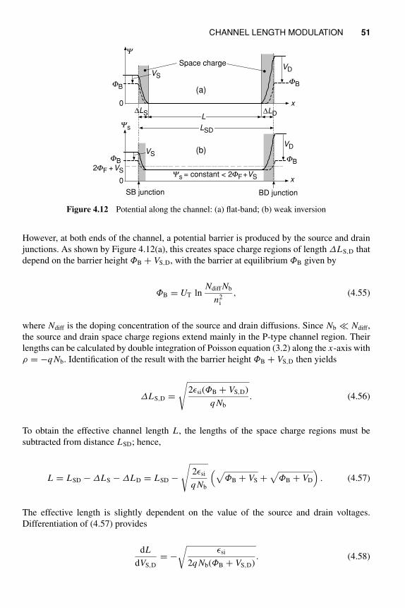
CHANNEL LENGTH MODULATION 51
(a)
(b)
SB junction BD junction
x
x
Ys
Y
0
0
FBFB
FB FB2FF +VS
VS
VS
VD
VD
∆LS ∆LD
Space charge
Ys = constant < 2FF+VS
L
LSD
Figure 4.12 Potential along the channel: (a) flat-band; (b) weak inversion
However, at both ends of the channel, a potential barrier is produced by the source and drain
junctions. As shown by Figure 4.12(a), this creates space charge regions of length ΔLS,D that
depend on the barrier height ΦB + VS,D, with the barrier at equilibrium ΦB given by
ΦB = UT lnNdiff Nb
n2i
, (4.55)
where Ndiff is the doping concentration of the source and drain diffusions. Since Nb ≪ Ndiff,
the source and drain space charge regions extend mainly in the P-type channel region. Their
lengths can be calculated by double integration of Poisson equation (3.2) along the x-axis with
ρ = −q Nb. Identification of the result with the barrier height ΦB + VS,D then yields
ΔLS,D =
√
2ǫsi(ΦB + VS,D)
q Nb
. (4.56)
To obtain the effective channel length L , the lengths of the space charge regions must be
subtracted from distance LSD; hence,
L = LSD − ΔLS − ΔLD = LSD −
√
2ǫsi
q Nb
(√
ΦB + VS +√
ΦB + VD
)
. (4.57)
The effective length is slightly dependent on the value of the source and drain voltages.
Differentiation of (4.57) provides
dL
dVS,D
= −√
ǫsi
2q Nb(ΦB + VS,D). (4.58)
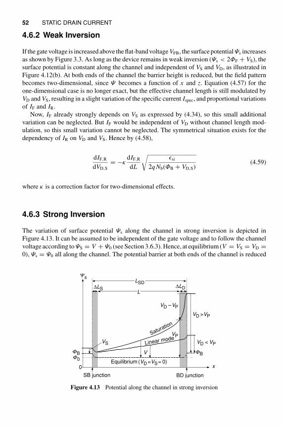
52 STATIC DRAIN CURRENT
4.6.2 Weak Inversion
If the gate voltage is increased above the flat-band voltage VFB, the surface potentialΨs increases
as shown by Figure 3.3. As long as the device remains in weak inversion (Ψs < 2ΦF + VS), the
surface potential is constant along the channel and independent of VS and VD, as illustrated in
Figure 4.12(b). At both ends of the channel the barrier height is reduced, but the field pattern
becomes two-dimensional, since Ψ becomes a function of x and z. Equation (4.57) for the
one-dimensional case is no longer exact, but the effective channel length is still modulated by
VD and VS, resulting in a slight variation of the specific current Ispec, and proportional variations
of IF and IR.
Now, IF already strongly depends on VS as expressed by (4.34), so this small additional
variation can be neglected. But IF would be independent of VD without channel length mod-
ulation, so this small variation cannot be neglected. The symmetrical situation exists for the
dependency of IR on VD and VS. Hence by (4.58),
dIF,R
dVD,S
= −κdIF,R
dL
√ǫsi
2q Nb(ΦB + VD,S)(4.59)
where κ is a correction factor for two-dimensional effects.
4.6.3 Strong Inversion
The variation of surface potential Ψs along the channel in strong inversion is depicted in
Figure 4.13. It can be assumed to be independent of the gate voltage and to follow the channel
voltage according to ΨS = V + Ψ0 (see Section 3.6.3). Hence, at equilibrium (V = VS = VD =0), Ψs = Ψ0 all along the channel. The potential barrier at both ends of the channel is reduced
SB junction BD junction
x
Ys
0
FB FB
VS
∆LS ∆LDL
LSD
F0
V
VD < VP
VP
VD >VP
Equilibrium (VD =VS= 0)
Linear modeSaturation
VD – VP
Figure 4.13 Potential along the channel in strong inversion
CHANNEL LENGTH MODULATION 53
to ΦB − Ψ0. Since Ψ0∼= 2ΦF, combining (3.8) and (4.55) gives
ΦB − Ψ0∼= UT ln
Ndiff
Nb
. (4.60)
For VS and VD > 0, this barrier remains constant as long as the transistor is in linear mode
(VD < VP). Hence, effective channel length L remains constant. If the transistor is saturated
with VD − VP > 0, the drain barrier is increased by the same amount; the forward current
becomes slightly dependent on the drain voltage. A symmetrical situations exists in reverse
saturation. Thus, similar to (4.59) with a different barrier height
dIF,R
dVD,S
= −κdIF,R
dL
√ǫsi
2q Nb(ΦB − Ψ0 + VD,S − VP). (4.61)
Experiments show that factor κ correcting for two-dimensional effects tends to decrease when
the inversion coefficient I C is increased.
4.6.4 Geometrical Effects
For the usual case of constant width W, Ispec given by (4.14) is inversely proportional to L .
Hence
−dIF,R
dL=
IF,R
L, (4.62)
and the effect of channel length modulation is identical in forward and reverse saturation.
We have seen in Section 4.5 that the fundamental property of the transistor, which includes
symmetrical source–drain characteristics, is independent of the channel geometry. But channel
length modulation degrades this property and is itself sensitive to device geometry.
As an example, consider again a concentric circular transistor with a radius RS of the source
and an inner radius RD = RS + L of the drain. According to equations (4.43) and (4.46),
IF ∝1
ln (1 + L/RS); (4.63)
hence,
−dIF
dL=
IF
RD ln RD/RS
=IF
L
1 − RS/RD
ln (RD/RS), (4.64)
which is smaller than result (4.62) for a rectangular channel.
Now if the transistor is in the reverse mode, its saturation current is −IR and channel length
modulation occurs at the source end of the channel. Thus, (4.63) can be rewritten as
IR ∝1
ln RD
RD−L
, (4.65)
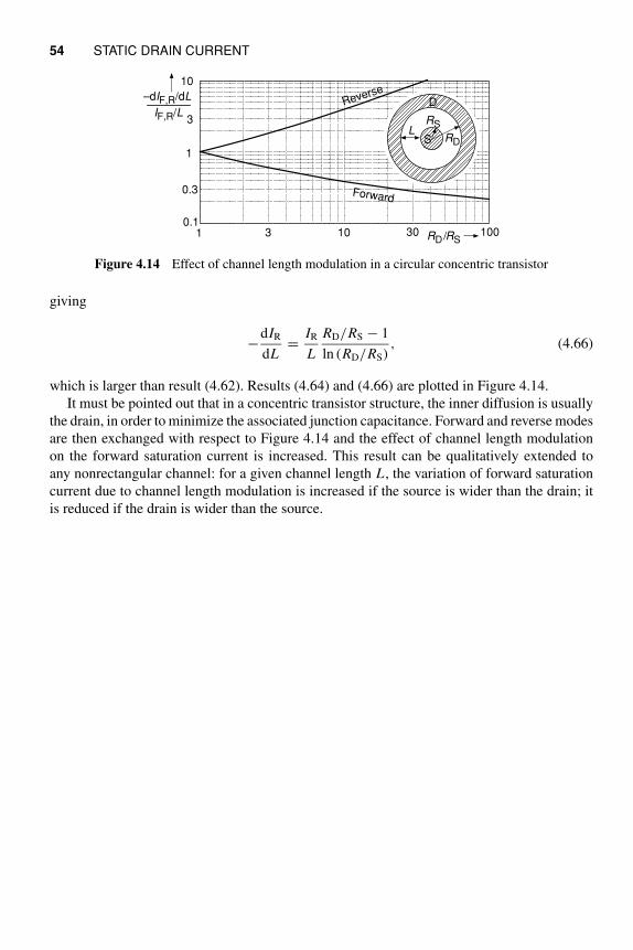
54 STATIC DRAIN CURRENT
Reverse
Forward
1 10 303 1000.1
0.3
1
3
10
RS
RDL
D
S
RD /RS
–dIF,R/dL
IF,R/L
Figure 4.14 Effect of channel length modulation in a circular concentric transistor
giving
−dIR
dL=
IR
L
RD/RS − 1
ln (RD/RS), (4.66)
which is larger than result (4.62). Results (4.64) and (4.66) are plotted in Figure 4.14.
It must be pointed out that in a concentric transistor structure, the inner diffusion is usually
the drain, in order to minimize the associated junction capacitance. Forward and reverse modes
are then exchanged with respect to Figure 4.14 and the effect of channel length modulation
on the forward saturation current is increased. This result can be qualitatively extended to
any nonrectangular channel: for a given channel length L , the variation of forward saturation
current due to channel length modulation is increased if the source is wider than the drain; it
is reduced if the drain is wider than the source.
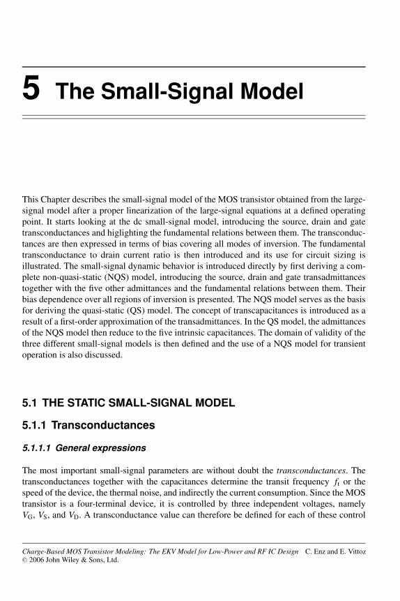
5 The Small-Signal Model
This Chapter describes the small-signal model of the MOS transistor obtained from the large-
signal model after a proper linearization of the large-signal equations at a defined operating
point. It starts looking at the dc small-signal model, introducing the source, drain and gate
transconductances and higlighting the fundamental relations between them. The transconduc-
tances are then expressed in terms of bias covering all modes of inversion. The fundamental
transconductance to drain current ratio is then introduced and its use for circuit sizing is
illustrated. The small-signal dynamic behavior is introduced directly by first deriving a com-
plete non-quasi-static (NQS) model, introducing the source, drain and gate transadmittances
together with the five other admittances and the fundamental relations between them. Their
bias dependence over all regions of inversion is presented. The NQS model serves as the basis
for deriving the quasi-static (QS) model. The concept of transcapacitances is introduced as a
result of a first-order approximation of the transadmittances. In the QS model, the admittances
of the NQS model then reduce to the five intrinsic capacitances. The domain of validity of the
three different small-signal models is then defined and the use of a NQS model for transient
operation is also discussed.
5.1 THE STATIC SMALL-SIGNAL MODEL
5.1.1 Transconductances
5.1.1.1 General expressions
The most important small-signal parameters are without doubt the transconductances. The
transconductances together with the capacitances determine the transit frequency ft or the
speed of the device, the thermal noise, and indirectly the current consumption. Since the MOS
transistor is a four-terminal device, it is controlled by three independent voltages, namely
VG, VS, and VD. A transconductance value can therefore be defined for each of these control
Charge-Based MOS Transistor Modeling: The EKV Model for Low-Power and RF IC Design C. Enz and E. VittozC© 2006 John Wiley & Sons, Ltd.
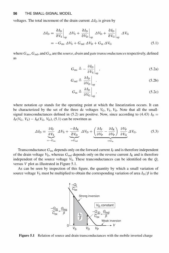
56 THE SMALL-SIGNAL MODEL
voltages. The total increment of the drain current ∆ID is given by
∆ID =∂ID
∂VS
∣∣∣∣op
∆VS +∂ID
∂VD
∣∣∣∣op
∆VD +∂ID
∂VG
∣∣∣∣op
∆VG
= −Gms ∆VS + Gmd ∆VD + Gm ∆VG (5.1)
where Gms, Gmd, and Gm are the source, drain and gate transconductances respectively, defined
as
Gms −∂ ID
∂VS
∣∣∣∣op
, (5.2a)
Gmd ∂ ID
∂VD
∣∣∣∣op
. (5.2b)
Gm ∂ ID
∂VG
∣∣∣∣op
, (5.2c)
where notation op stands for the operating point at which the linearization occurs. It can
be characterized by the set of the three dc voltages VG, VS, VD. Note that all the small-
signal transconductances defined in (5.2) are positive. Now, since according to (4.43) ID =IF(VG, VS) − IR(VG, VD), (5.1) can be rewritten as
∆ID =∂ IF
∂VS︸︷︷︸
=−Gms
∆VS +−∂IR
∂VD︸ ︷︷ ︸
=Gmd
∆VD +(
∂ IF
∂VP
−∂ IR
∂VP
)∂VP
∂VG︸ ︷︷ ︸
=Gm
∆VG. (5.3)
Transconductance Gms depends only on the forward current IF and is therefore independent
of the drain voltage VD, whereas Gmd depends only on the reverse current IR and is therefore
independent of the source voltage VS. These tranconductances can be identified on the Qi
versus V plot as illustrated in Figure 5.1.
As can be seen by inspection of this figure, the quantity by which a small variation of
source voltage VS must be multiplied to obtain the corresponding variation of area ID/β is the
IDb
VVP
–Q iCox
VS VD0
Strong inversion
Weak inversion
VG constantGmsb
iSCox
= Gmdb
–Q–Q
iDCox
=
Figure 5.1 Relation of source and drain transconductances with the mobile inverted charge
THE STATIC SMALL-SIGNAL MODEL 57
particular value −QiS/Cox of −Qi/Cox taken at the source end of the channel. Hence,
Gms =β
Cox
(−QiS) = μW
L(−QiS) = Gspec qs (5.4)
and, symmetrically,
Gmd =β
Cox
(−QiD) = μW
L(−QiD) = Gspec qd, (5.5)
where
Gspec Ispec/UT = 2nβUT, (5.6)
and qs and qd are the normalized charges at both ends of the channel defined by
qs −QiS
Qspec
, (5.7a)
qd −QiD
Qspec
. (5.7b)
Note that the two expressions (5.4) and (5.5) are very general, and do not depend on the
precise shape of −Qi(V ).
As shown by (4.25), IF and IR depend on the differences VP − VS and VP − VD respectively.
A variation of VS or VD has the same effect on IF and IR as an equal variation of VP of opposite
sign. Therefore we have
∂ IF
∂VP
= Gms and∂ IR
∂VP
= Gmd. (5.8)
Furthermore, according to (3.51), dVP/dVG = 1/n. Hence the expression of Gm in (5.3) be-
comes
Gm =Gms − Gmd
n. (5.9)
Note that this dependency of the gate transconductance on the source and drain transcon-
ductances Gms and Gmd is independent of the inversion coefficient of the transistor.
When the transistor is saturated, IR ≪ IF and Gmd ≪ Gms and hence
Gm =Gms
n(saturation). (5.10)
Using the normalized charges qs and qd given in (4.24), expressions (5.4) and (5.5) become
gms,d Gms,d
Gspec
= qs,d =
√4if,r + 1 − 1
2=
2if,r√
4if,r + 1 + 1, (5.11)
58 THE SMALL-SIGNAL MODEL
or, by using denormalized variables,
Gms,d = nβUT
(√
4IF,R/Ispec + 1 − 1)
. (5.12)
The gate transconductance can be obtained by introducing this expression in (5.9), giving
Gm = βUT
(√
4IF/Ispec + 1 −√
4IR/Ispec + 1)
. (5.13)
However, this result is useful only if the forward and reverse currents are known separately
(and not only their difference ID = IF − IR).
Since relation (3.48) between voltages and charge cannot be inverted, the transconductances
cannot be expressed as functions of voltages in the general case.
5.1.1.2 Approximation in strong inversion
With the strong inversion approximation of the charge discussed in Section 3.6.3, the various
transconductances can be found directly on the VTB(V ) plot of Figure 3.12(a), as shown in
Figure 5.2(a).
This diagram, which also shows the current in function of the bias voltages, will be called
the Jespers–Memelink diagram [15,77]. It can be used to analyze and synthesize circuits using
transistors in strong inversion. Expression (5.9) of the gate transconductance can be verified
by simple inspection of this diagram.
The expressions of the source and drain transconductances can be obtained by differentiating
the current given by (4.28) or simply by inspection of Figure 5.2.
If β, VS,D, and VP (or VG) are known, this figure shows that
Gms,d = nβ(VP − VS,D) = β(VG − VT0 − nVS,D). (5.14)
Slo
pe n
VG
VTB
VVP
VT0
00
VS VD
Gmsb
Gmb
GmdbID
b Slope – n
VP
–Q iCox
VG – VT0
0
VG const.
(b)
0VS VD
Gmsb Gmd
bGmb
(a)
Figure 5.2 Drain current and transconductances in strong inversion: (a) Jespers–Memelink diagram;
(b) corresponding Qi (V ) plot
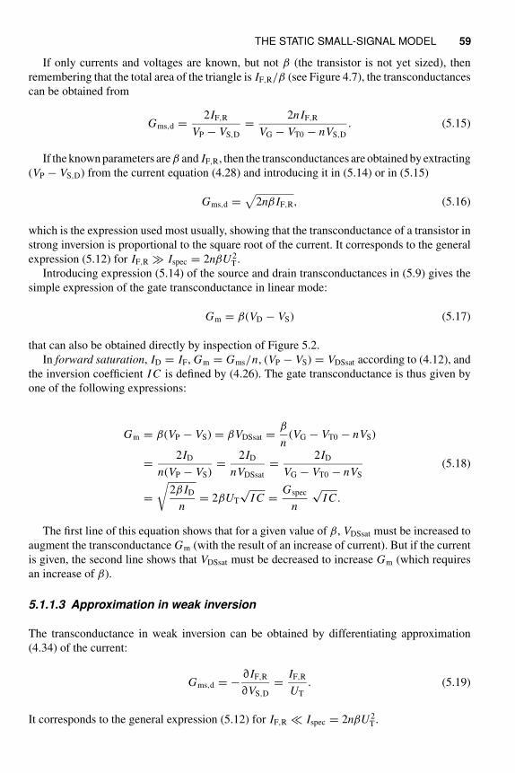
THE STATIC SMALL-SIGNAL MODEL 59
If only currents and voltages are known, but not β (the transistor is not yet sized), then
remembering that the total area of the triangle is IF,R/β (see Figure 4.7), the transconductances
can be obtained from
Gms,d =2IF,R
VP − VS,D
=2nIF,R
VG − VT0 − nVS,D
. (5.15)
If the known parameters areβ and IF,R, then the transconductances are obtained by extracting
(VP − VS,D) from the current equation (4.28) and introducing it in (5.14) or in (5.15)
Gms,d =√
2nβ IF,R, (5.16)
which is the expression used most usually, showing that the transconductance of a transistor in
strong inversion is proportional to the square root of the current. It corresponds to the general
expression (5.12) for IF,R ≫ Ispec = 2nβU 2T .
Introducing expression (5.14) of the source and drain transconductances in (5.9) gives the
simple expression of the gate transconductance in linear mode:
Gm = β(VD − VS) (5.17)
that can also be obtained directly by inspection of Figure 5.2.
In forward saturation, ID = IF, Gm = Gms/n, (VP − VS) = VDSsat according to (4.12), and
the inversion coefficient I C is defined by (4.26). The gate transconductance is thus given by
one of the following expressions:
Gm = β(VP − VS) = βVDSsat =β
n(VG − VT0 − nVS)
=2ID
n(VP − VS)=
2ID
nVDSsat
=2ID
VG − VT0 − nVS
(5.18)
=
√
2β ID
n= 2βUT
√I C =
Gspec
n
√I C .
The first line of this equation shows that for a given value of β, VDSsat must be increased to
augment the transconductance Gm (with the result of an increase of current). But if the current
is given, the second line shows that VDSsat must be decreased to increase Gm (which requires
an increase of β).
5.1.1.3 Approximation in weak inversion
The transconductance in weak inversion can be obtained by differentiating approximation
(4.34) of the current:
Gms,d = −∂IF,R
∂VS,D
=IF,R
UT
. (5.19)
It corresponds to the general expression (5.12) for IF,R ≪ Ispec = 2nβU 2T .
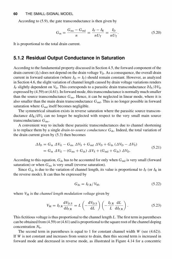
60 THE SMALL-SIGNAL MODEL
According to (5.9), the gate transconductance is then given by
Gm =Gms − Gmd
n=
IF − IR
nUT
=ID
nUT
. (5.20)
It is proportional to the total drain current.
5.1.2 Residual Output Conductance in Saturation
According to the fundamental property discussed in Section 4.5, the forward component of the
drain current (IF) does not depend on the drain voltage VD. As a consequence, the overall drain
current in forward saturation (where ID = IF) should remain constant. However, as analyzed
in Section 4.6, the slight variation of channel length caused by drain voltage variations renders
IF slightly dependent on VD. This corresponds to a parasitic drain transconductance ∂IF/∂VD
expressed by (4.59) or (4.61). In forward mode, this transconductance is normally much smaller
than the source transconductance Gms. Hence, it can be neglected in linear mode, where it is
also smaller than the main drain transconductance Gmd. This is no longer possible in forward
saturation where Gmd itself becomes negligible.
The symmetrical situation exists in reverse saturation where the parasitic source transcon-
ductance dIR/dVS can no longer be neglected with respect to the very small main source
transconductance Gms.
A convenient way to include these parasitic transconductances due to channel shortening
is to replace them by a single drain-to-source conductance Gds. Indeed, the total variation of
the drain current given by (5.3) then becomes
∆ID = Gm ∆VG − Gms ∆VS + Gmd ∆VD + Gds (∆VD − ∆VS)
= Gm ∆VG − (Gms + Gds) ∆VS + (Gmd + Gds) ∆VD.(5.21)
According to this equation, Gds has to be accounted for only when Gmd is very small (forward
saturation) or when Gms is very small (reverse saturation).
Since Gds is due to the variation of channel length, its value is proportional to IF (or IR in
the reverse mode). It can thus be expressed by
Gds = IF,R/VM, (5.22)
where VM is the channel length modulation voltage given by
VM = IF,R
dVD,S
dIF,R
= L
(
−dVD,S
dL
)(
−IF,R
L
dL
dIF,R
)
. (5.23)
This fictitious voltage is thus proportional to the channel length L . The first term in parentheses
can be obtained from (4.59) or (4.61) and is proportional to the square root of the channel doping
concentration Nb.
The second term in parentheses is equal to 1 for constant channel width W (see (4.62)).
If W is not constant and increases from source to drain, then this second term is increased in
forward mode and decreased in reverse mode, as illustrated in Figure 4.14 for a concentric
THE STATIC SMALL-SIGNAL MODEL 61
0
VG1
VG2
–VMVD
IF2
IF1
ID
Slope Gds
Figure 5.3 Convergence of saturation characteristics toward −VM
circular transistor. The value of VM is thus increased (hence Gds decreased) if the saturated
side of the transistor is wider and decreased (hence Gds increased) in the opposite case.
Assuming VM ≫ VD,S (long channel) and constant, it corresponds to the convergence point
of saturation currents for various gate voltages, as illustrated in Figure 5.3. In reality, due to
two-dimensional effects, VM tends to increase slowly when the inversion coefficient I C is
increased.
5.1.3 Equivalent Circuit
The small-signal equivalent circuit of the transistor, which corresponds to equation (5.21), is
shown in Figure 5.4.
The three transconductances discussed in Section 5.1.1 are represented by voltage-
controlled current sources (VCCS) of adequate sign connected between the source and drain
nodes. The residual conductance in saturation Gds, introduced in Section 5.1.2, is connected
in parallel. Note that the small-signal schematic of Figure 5.4 includes only the intrinsic com-
ponents of the transistor.
The expressions of the intrinsic parameters, derived previously as function of bias voltages
and/or currents, are summarized in Table 5.1 for weak and strong inversion.
A new parameter Av max defined by
Av max Gms
Gds
(5.24)
is introduced at the last row of this table. It is the maximum voltage gain available from the
transistor in common gate configuration (driven from the source with ∆VG = 0). Indeed, if
Gm ∆VG
Gms ∆VS
Gmd ∆VD
Gds
B
S∆ID
D
B
∆VS ∆VD
∆VG
G
Figure 5.4 Small-signal dc equivalent circuit
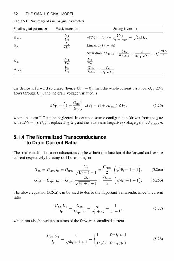
62 THE SMALL-SIGNAL MODEL
Table 5.1 Summary of small-signal parameters
Small-signal parameter Weak inversion Strong inversion
Gms,dIF,R
UTnβ(VP − VS,D) = 2IF,R
VP − VS,D=
√2nβ IF,R
GmID
nUTLinear: β(VD − VS)
Saturation: βVDSsat = 2ID
nVDSsat= ID
nUT
√I C
=√
2β IDn
GdsIF,R
VM
IF,R
VM
Av maxVM
UT
2VM
VDSsat= VM
UT
√I C
the device is forward saturated (hence Gmd = 0), then the whole current variation Gms ∆VS
flows through Gds, and the drain voltage variation is
∆VD =(
1 +Gms
Gds
)
∆VS = (1 + Av max) ∆VS, (5.25)
where the term “1” can be neglected. In common source configuration (driven from the gate
with ∆VS = 0), Gms is replaced by Gm and the maximum (negative) voltage gain is Av max/n.
5.1.4 The Normalized Transconductanceto Drain Current Ratio
The source and drain transconductances can be written as a function of the forward and reverse
current respectively by using (5.11), resulting in
Gms = Gspec qs = Gspec
2if√4if + 1 + 1
=Gspec
2
(√
4if + 1 − 1)
, (5.26a)
Gmd = Gspec qd = Gspec
2ir√4ir + 1 + 1
=Gspec
2
(√
4ir + 1 − 1)
. (5.26b)
The above equation (5.26a) can be used to derive the important transconductance to current
ratio
Gms UT
IF
=Gms
Gspec if
=qs
q2s + qs
=1
qs + 1, (5.27)
which can also be written in terms of the forward normalized current
Gms UT
IF
=2
√4if + 1 + 1
=
1 for if ≪ 1
1/√
if for if ≫ 1.(5.28)
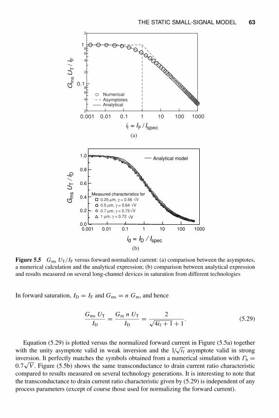
THE STATIC SMALL-SIGNAL MODEL 63
2
4
6
80.1
2
4
6
81
2
Gm
sU
T / IF
0.001 0.01 0.1 1 10 100 1000
if = IF / Ispec
Numerical Asymptotes Analytical
(a)
Analytical model
Measured characteristics for
Gm
s U
T / I
D
id = ID / Ispec
0.001 0.01 0.1 1 10 100 1000
1.0
0.8
0.6
0.4
0.2
0.0
0.25 µm, γ = 0.56 V
0.5 µm, γ = 0.64 V
0.7 µm, γ = 0.75
1 µm, γ = 0.72
V
(b)
Figure 5.5 Gms UT/IF versus forward normalized current: (a) comparison between the asymptotes,
a numerical calculation and the analytical expression; (b) comparison between analytical expression
and results measured on several long-channel devices in saturation from different technologies
In forward saturation, ID = IF and Gms = n Gm, and hence
Gms UT
ID
=Gm n UT
ID
=2
√4if + 1 + 1
. (5.29)
Equation (5.29) is plotted versus the normalized forward current in Figure (5.5a) together
with the unity asymptote valid in weak inversion and the 1/√
if asymptote valid in strong
inversion. It perfectly matches the symbols obtained from a numerical simulation with Γb =0.7
√V . Figure (5.5b) shows the same transconductance to drain current ratio characteristic
compared to results measured on several technology generations. It is interesting to note that
the transconductance to drain current ratio characteristic given by (5.29) is independent of any
process parameters (except of course those used for normalizing the forward current).
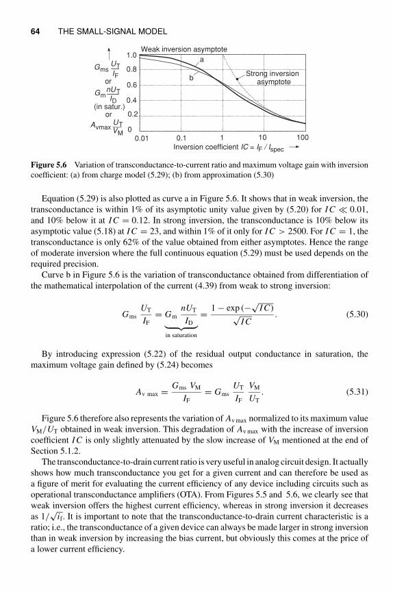
64 THE SMALL-SIGNAL MODEL
0.01 0.1 1 10 1000
0.2
0.4
0.6
0.8
1.0
Inversion coefficient IC = IF / Ispec
GmsUTIF
GmnUTID
(in satur.)
AvmaxUTVM
or
Weak inversion asymptote
Strong inversionasymptote
a
b
or
Figure 5.6 Variation of transconductance-to-current ratio and maximum voltage gain with inversion
coefficient: (a) from charge model (5.29); (b) from approximation (5.30)
Equation (5.29) is also plotted as curve a in Figure 5.6. It shows that in weak inversion, the
transconductance is within 1% of its asymptotic unity value given by (5.20) for I C ≪ 0.01,
and 10% below it at I C = 0.12. In strong inversion, the transconductance is 10% below its
asymptotic value (5.18) at I C = 23, and within 1% of it only for I C > 2500. For I C = 1, the
transconductance is only 62% of the value obtained from either asymptotes. Hence the range
of moderate inversion where the full continuous equation (5.29) must be used depends on the
required precision.
Curve b in Figure 5.6 is the variation of transconductance obtained from differentiation of
the mathematical interpolation of the current (4.39) from weak to strong inversion:
Gms
UT
IF
= Gm
nUT
ID︸ ︷︷ ︸
in saturation
=1 − exp (−
√I C)
√I C
. (5.30)
By introducing expression (5.22) of the residual output conductance in saturation, the
maximum voltage gain defined by (5.24) becomes
Av max =Gms VM
IF
= Gms
UT
IF
VM
UT
. (5.31)
Figure 5.6 therefore also represents the variation of Av max normalized to its maximum value
VM/UT obtained in weak inversion. This degradation of Av max with the increase of inversion
coefficient I C is only slightly attenuated by the slow increase of VM mentioned at the end of
Section 5.1.2.
The transconductance-to-drain current ratio is very useful in analog circuit design. It actually
shows how much transconductance you get for a given current and can therefore be used as
a figure of merit for evaluating the current efficiency of any device including circuits such as
operational transconductance amplifiers (OTA). From Figures 5.5 and 5.6, we clearly see that
weak inversion offers the highest current efficiency, whereas in strong inversion it decreases
as 1/√
if. It is important to note that the transconductance-to-drain current characteristic is a
ratio; i.e., the transconductance of a given device can always be made larger in strong inversion
than in weak inversion by increasing the bias current, but obviously this comes at the price of
a lower current efficiency.
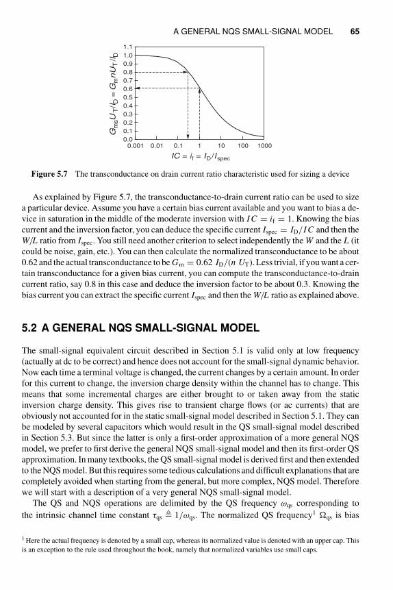
A GENERAL NQS SMALL-SIGNAL MODEL 65
1.1
1.0
0.9
0.8
0.7
0.6
0.5
0.4
0.3
0.2
0.1
0.0
Gm
sUT / I
D =
Gm
nU
T / I D
0.001 0.01 0.1 1 10 100 1000
IC = i f = I D / I spec
Figure 5.7 The transconductance on drain current ratio characteristic used for sizing a device
As explained by Figure 5.7, the transconductance-to-drain current ratio can be used to size
a particular device. Assume you have a certain bias current available and you want to bias a de-
vice in saturation in the middle of the moderate inversion with I C = if = 1. Knowing the bias
current and the inversion factor, you can deduce the specific current Ispec = ID/I C and then the
W/L ratio from Ispec. You still need another criterion to select independently the W and the L (it
could be noise, gain, etc.). You can then calculate the normalized transconductance to be about
0.62 and the actual transconductance to be Gm = 0.62 ID/(n UT). Less trivial, if you want a cer-
tain transconductance for a given bias current, you can compute the transconductance-to-drain
current ratio, say 0.8 in this case and deduce the inversion factor to be about 0.3. Knowing the
bias current you can extract the specific current Ispec and then the W/L ratio as explained above.
5.2 A GENERAL NQS SMALL-SIGNAL MODEL
The small-signal equivalent circuit described in Section 5.1 is valid only at low frequency
(actually at dc to be correct) and hence does not account for the small-signal dynamic behavior.
Now each time a terminal voltage is changed, the current changes by a certain amount. In order
for this current to change, the inversion charge density within the channel has to change. This
means that some incremental charges are either brought to or taken away from the static
inversion charge density. This gives rise to transient charge flows (or ac currents) that are
obviously not accounted for in the static small-signal model described in Section 5.1. They can
be modeled by several capacitors which would result in the QS small-signal model described
in Section 5.3. But since the latter is only a first-order approximation of a more general NQS
model, we prefer to first derive the general NQS small-signal model and then its first-order QS
approximation. In many textbooks, the QS small-signal model is derived first and then extended
to the NQS model. But this requires some tedious calculations and difficult explanations that are
completely avoided when starting from the general, but more complex, NQS model. Therefore
we will start with a description of a very general NQS small-signal model.
The QS and NQS operations are delimited by the QS frequency ωqs corresponding to
the intrinsic channel time constant τqs 1/ωqs. The normalized QS frequency1 qs is bias
1 Here the actual frequency is denoted by a small cap, whereas its normalized value is denoted with an upper cap. This
is an exception to the rule used throughout the book, namely that normalized variables use small caps.
66 THE SMALL-SIGNAL MODEL
dependent according to [44]:
qs ωqs
ωspec
τspec
τqs
= 30(qs + qd + 1)3
4q2s + 4q2
d + 12qsqd + 10qs + 10qd + 5, (5.32)
where
ωspec =1
τspec
µ UT
L2. (5.33)
The QS channel cutoff frequency ωqs can be used as a figure of merit since it represents the
ultimate frequency that the intrinsic part of the MOS transistor can reach without accounting
for the extrinsic components such as the overlap capacitors that further decrease this frequency
and are accounted for in the transit frequency ft discussed in Section 11.3.1. Notice that ωspec
scales like 1/L2, therefore increasing quadratically when reducing the transistor length. This
feature is one of the driving force for CMOS downscaling to achieve faster circuits and also
use CMOS for RF circuits.
In saturation (qs ≫ qd), (5.32) reduces to
qs∼= 30
(qs + 1)3
4q2s + 10qs + 5
=
⎧
⎨
⎩
6 (weak inv.)
152
qs = 152
√if = 15
4VP−VS
UT(strong inv.).
(5.34)
From (5.34), we see that in weak inversion ωqs = 6ωspec = 6μ UT/L2, which is constant
and determined only by the mobility and the transistor length. Note that in weak inversion,
τqs = 1/ωqs corresponds to the transit time of the carriers diffusing from source to drain.
In strong inversion, qs is proportional to qs or to√
if or to the saturation voltage VD Ssat =VP − VS.
For VD = VS (or equivalently qs = qd), (5.32) reduces to
qs∼= 6 (2qs + 1). (5.35)
The normalized QS frequency qs is plotted versus the inversion factor if in Figure 5.8(a)
which clearly shows the weak and strong inversion asymptotes. Notice that in strong inversion
and for VD = VS, qs is 1.6 times larger than in saturation for the same inversion factor. qs is
also plotted versus the normalized pinch-off voltage vp in Figure 5.8(b) for different values of
the normalized drain voltage ranging from vd = 0 to vd = 100, corresponding to saturation.
Also shown is the strong inversion asymptote 15/4 vp.
The NQS analysis will not be detailed here, since it is rather lengthy. It can be found in
[38,44,78]. The most important result of the latter analysis is that the NQS small-signal behavior
can be represented by the equivalent small-signal circuit presented in Figure 5.9. This circuit is
made of five admittances, three connected to the gate (YGSi, YGDi, and YGBi) and two connected
to the bulk (YBSi, YBDi) not accounting for YGBi and three transadmittances Ym, Yms, and Ymd
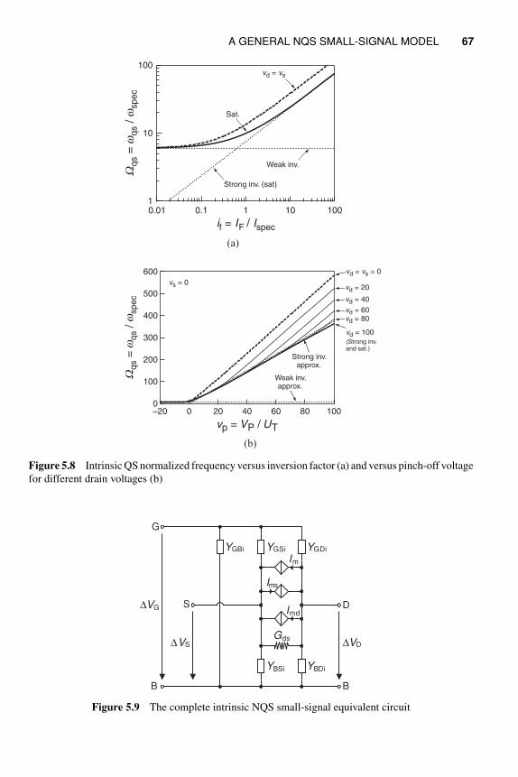
A GENERAL NQS SMALL-SIGNAL MODEL 67
1
10
100
Wq
s =
wq
s /
wsp
ec
0.01 0.1 1 10 100
if = IF / Ispec
vd = vs
Sat.
Strong inv. (sat)
Weak inv.
(a)
600
500
400
300
200
100
0
Wq
s =
wq
s / w
sp
ec
100806040200–20
vp = VP / UT
vd = vs = 0
vd = 20
vd = 40
vd = 60vd = 80
vd = 100
(Strong inv.and sat.)
Strong inv.approx.
Weak inv.approx.
vs = 0
(b)
Figure 5.8 Intrinsic QS normalized frequency versus inversion factor (a) and versus pinch-off voltage
for different drain voltages (b)
BB
Im
Ims
Imd
Gds
G
DS
YGSi YGDiYGBi
YBSi YBDi
∆VG
∆VS ∆VD
Figure 5.9 The complete intrinsic NQS small-signal equivalent circuit
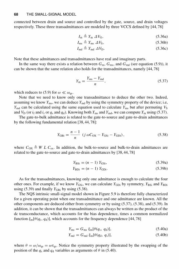
68 THE SMALL-SIGNAL MODEL
connected between drain and source and controlled by the gate, source, and drain voltages
respectively. These three transadmittances are modeled by three VCCS defined by [44, 78]
Im Ym ∆VG, (5.36a)
Ims Yms ∆VS, (5.36b)
Imd Ymd ∆VD. (5.36c)
Note that these admittances and transadmittances have real and imaginary parts.
In the same way there exists a relation between Gm, Gms, and Gmd (see equation (5.9)), it
can be shown that the same relation also holds for the transadmittances, namely [44, 78]
Ym =Yms − Ymd
n, (5.37)
which reduces to (5.9) for ω ≪ ωqs.
Note that we need to know only one transadmittance to deduce the other two. Indeed,
assuming we know Yms, we can deduce Ymd by using the symmetry property of the device; i.e,
Ymd can be calculated using the same equation used to calculate Yms but after permuting VS
and VD (or if and ir or qs and qd). Knowing both Yms and Ymd, we can compute Ym using (5.37).
The gate-to-bulk admittance is related to the gate-to-source and gate-to-drain admittances
by the following fundamental relation [38, 44, 78]:
YGBi =n − 1
n( j ωCOX − YGSi − YGDi) , (5.38)
where COX W L Cox. In addition, the bulk-to-source and bulk-to-drain admittances are
related to the gate-to-source and gate-to-drain admittances by [38, 44, 78]
YBSi = (n − 1) YGSi, (5.39a)
YBDi = (n − 1) YGDi. (5.39b)
As for the transadmittances, knowing only one admittance is enough to calculate the four
other ones. For example, if we know YGSi, we can calculate YGDi by symmetry, YBSi and YBDi
using (5.39) and finally YGBi by using (5.38).
The NQS intrinsic small-signal model shown in Figure 5.9 is therefore fully characterized
for a given operating point when one transadmittance and one admittance are known. All the
other components are deduced either from symmetry or by using (5.37), (5.38), and (5.39). In
addition, it can be shown that the transadmittances can always be written as the product of the
dc transconductance, which accounts for the bias dependence, times a common normalized
function ξm[θ (qs, qd)], which accounts for the frequency dependence [44, 78]
Yms = Gms ξm[θ (qs, qd)], (5.40a)
Ymd = Gmd ξm[θ (qd, qs)], (5.40b)
where θ = ω/ωqs = ωτqs. Notice the symmetry property illustrated by the swapping of the
position of the qs and qd variables as arguments of θ in (5.40).
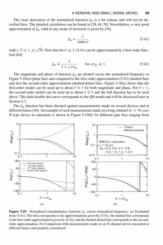
A GENERAL NQS SMALL-SIGNAL MODEL 69
The exact derivation of the normalized function ξm is a bit tedious and will not be de-
scribed here. The detailed calculation can be found in [38, 44, 78]. Nevertheless, a very good
approximation of ξm valid in any mode of inversion is given by [44]
ξm =λ
sinh(λ), (5.41)
with λ (1 + j)√
3θ . Note that for θ ≪ 1, (5.41) can be approximated by a first-order func-
tion [44]
ξm∼=
1
1 + j ωτqs
for ωτqs ≪ 1. (5.42)
The magnitude and phase of function ξm are plotted versus the normalized frequency in
Figure 5.10(a) (plain line) and compared to the first-order approximation (5.42) (dashed line)
and also the second-order approximation (dashed-dotted line). Figure 5.10(a) shows that the
first-order model can be used up to about θ ∼= 1 for both magnitude and phase. For θ > 1,
the second-order model can be used up to about θ ∼= 3 and the full function has to be used
above. The dash-double-dot curve corresponds to the QS model and will be discussed later in
Section 5.3.
The ξm function has been checked against measurements made on several devices and at
different biases [44]. An example of such measurements made on a long-channel (L = 10 μm)
N-type device in saturation is shown in Figure 5.10(b) for different gate bias ranging from
0.1
1
10
Mag( x
m )
0.1 1 10
–180
–90
0
90
180
Arg
( xm )
0.1 1 10
q = wtqs
Full nqs function 1st-order approx. 2nd-order approx. Quasi-static approx.
(a)
0.01
0.1
1
10
Ma
g( x
m )
0.1 1 10
–180
–90
0
90
180
Arg
( xm )
(d
eg
)
0.1 1 10
q = wtqs
NMOS in saturation
VG = 0.5, 0.6, 0.7, 0.8,
0.9, 1.0, 1.2, 1.5 V
Theory Measurements
(b)
L
Figure 5.10 Normalized transdmittance function ξm versus normalized frequency. (a) Evaluated
from (5.41). The line corresponds to the approximations given by (5.41), the dashed line corresponds
to the first-order approximation given by (5.42), and the dashed-dotted line corresponds to the second-
order approximation. (b) Comparison with measurements made on an N-channel device measured at
different biases and properly normalized
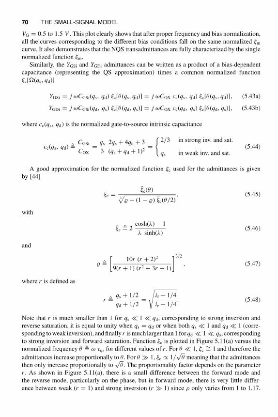
70 THE SMALL-SIGNAL MODEL
VG = 0.5 to 1.5 V . This plot clearly shows that after proper frequency and bias normalization,
all the curves corresponding to the different bias conditions fall on the same normalized ξm
curve. It also demonstrates that the NQS transadmittances are fully characterized by the single
normalized function ξm.
Similarly, the YGSi and YGDi admittances can be written as a product of a bias-dependent
capacitance (representing the QS approximation) times a common normalized function
ξc[(qs, qd)]
YGSi = j ωCGSi(qs, qd) ξc[θ (qs, qd)] = j ωCOX cc(qs, qd) ξc[θ (qs, qd)], (5.43a)
YGDi = j ωCGSi(qd, qs) ξc[θ (qd, qs)] = j ωCOX cc(qd, qs) ξc[θ (qd, qs)], (5.43b)
where cc(qs, qd) is the normalized gate-to-source intrinsic capacitance
cc(qs, qd) CGSi
COX
=qs
3
2qs + 4qd + 3
(qs + qd + 1)2=
2/3 in strong inv. and sat.
qs in weak inv. and sat.(5.44)
A good approximation for the normalized function ξc used for the admittances is given
by [44]
ξc =ξc(θ )
3√
+ (1 − ) ξc(θ/2), (5.45)
with
ξc 2cosh(λ) − 1
λ sinh(λ)(5.46)
and
[10r (r + 2)2
9(r + 1) (r2 + 3r + 1)
]3/2
, (5.47)
where r is defined as
r qs + 1/2
qd + 1/2=
√
if + 1/4
ir + 1/4. (5.48)
Note that r is much smaller than 1 for qs ≪ 1 ≪ qd, corresponding to strong inversion and
reverse saturation, it is equal to unity when qs = qd or when both qs ≪ 1 and qd ≪ 1 (corre-
sponding to weak inversion), and finally r is much larger than 1 for qd ≪ 1 ≪ qs, corresponding
to strong inversion and forward saturation. Function ξc is plotted in Figure 5.11(a) versus the
normalized frequency θ ω τqs for different values of r . For θ ≪ 1, ξc∼= 1 and therefore the
admittances increase proportionally to θ . For θ ≫ 1, ξc ∝ 1/√
θ meaning that the admittances
then only increase proportionally to√
θ . The proportionality factor depends on the parameter
r . As shown in Figure 5.11(a), there is a small difference between the forward mode and
the reverse mode, particularly on the phase, but in forward mode, there is very little differ-
ence between weak (r = 1) and strong inversion (r ≫ 1) since ρ only varies from 1 to 1.17.
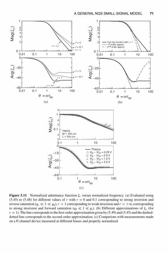
A GENERAL NQS SMALL-SIGNAL MODEL 71
0.1
2
3
456
1
Mag( x
c )
0.01 0.1 1 10 100
–60
–40
–20
0
Arg
( xc )
0.01 0.1 1 10 100
q = wtqs
r = 0
r = 0.1r = 1
r = +•
r = 0
r = 0.1r = 1
r = +•
(a)
0.1
2
3
4
56
1
Ma
g( x
c )
0.01 0.1 1 10 100
–60
–40
–20
0
Arg
( xc )
0.01 0.1 1 10 100
q = wtqs
Full nqs function with r = 1 1st-order approx. 2nd-order approx.
(b)
(c)
2
4
0.1
2
4
1
2
Ma
g( x
c )
0.1 1 10 100
–60
–45
–30
–15
0
Arg
( xc )
0.1 1 10 100q = wtqs
Theory
PMOS
VG – VT0 = 0.5 VVG – VT0 = 1.5 VVG – VT0 = 2.5 V
VG – VT0 = 0.25 V
WL
Figure 5.11 Normalized admittance function ξc versus normalized frequency. (a) Evaluated using
(5.45) to (5.48) for different values of r with r = 0 and 0.1 corresponding to strong inversion and
reverse saturation (qs ≪ 1 ≪ qd), r = 1 corresponding to weak inversion and r = +∞ corresponding
to strong inversion and forward saturation (qd ≪ 1 ≪ qs). (b) Different approximations of ξc (for
r = 1). The line corresponds to the first-order approximation given by (5.49) and (5.45) and the dashed-
dotted line corresponds to the second-order approximation. (c) Comparions with measurements made
on a P-channel device measured at different biases and properly normalized
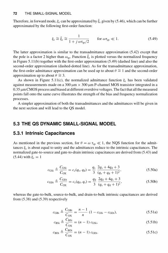
72 THE SMALL-SIGNAL MODEL
Therefore, in forward mode, ξc can be approximated by ξc given by (5.46), which can be further
approximated by the following first-order function:
ξc∼= ξc
∼=1
1 + j ωτqs/2for ωτqs ≪ 1. (5.49)
The latter approximation is similar to the transadmittance approximation (5.42) except that
the pole is a factor 2 higher than ωqs. Function ξc is plotted versus the normalized frequency
in Figure 5.11(b) together with the first-order approximation (5.49) (dashed line) and also the
second-order approximation (dashed-dotted line). As for the transadmittance approximation,
the first-order admittance approximation can be used up to about θ ∼= 1 and the second-order
approximation up to about θ ∼= 3.
As shown in Figure 5.11(c), the normalized admittance function ξc has been validated
against measurements made on a 300 μm × 300 μm P-channel MOS transistor integrated in a
0.35μm CMOS process and biased at different overdrive voltages. The fact that all the measured
points fall onto the same curve illustrates the strength of the bias and frequency normalization
processes.
A simpler approximation of both the transadmittances and the admittances will be given in
the next section and will lead to the QS model.
5.3 THE QS DYNAMIC SMALL-SIGNAL MODEL
5.3.1 Intrinsic Capacitances
As mentioned in the previous section, for θ = ω τqs ≪ 1, the NQS function for the admit-
tances ξc is about equal to unity and the admittances reduce to the intrinsic capacitances. The
normalized gate-to-source and gate-to-drain intrinsic capacitances are derived from (5.43) and
(5.44) with ξc = 1
cGSi CGSi
COX
= cc(qs, qd) =qs
3
2qs + 4qd + 3
(qs + qd + 1)2, (5.50a)
cGDi CGDi
COX
= cc(qd, qs) =qd
3
2qd + 4qs + 3
(qs + qd + 1)2, (5.50b)
whereas the gate-to-bulk, source-to-bulk, and drain-to-bulk intrinsic capacitances are derived
from (5.38) and (5.39) respectively
cGBi CGBi
COX
=n − 1
n(1 − cGSi − cGDi), (5.51a)
cBSi CBSi
COX
= (n − 1) cGSi, (5.51b)
cBDi CBDi
COX
= (n − 1) cGDi. (5.51c)
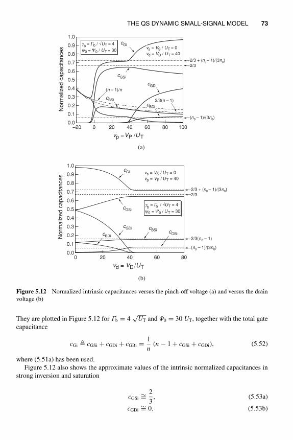
THE QS DYNAMIC SMALL-SIGNAL MODEL 73
1.0
0.9
0.8
0.7
0.6
0.5
0.4
0.3
0.2
0.1
0.0
Norm
aliz
ed c
apacitances
100806040200–20
vp =VP /UT
gb = Gb / √UT = 4
y0 = Y0 / UT = 30vs = VS / UT = 0
vd = VD / UT = 40
cGSi
cGi
cBSi
cGDi
cBDi
2/3 + (n0 – 1)/(3n0)2/3
2/3(n – 1)
(n0 – 1)/(3n0)
(n – 1)/n
(a)
(b)
1.0
0.9
0.8
0.7
0.6
0.5
0.4
0.3
0.2
0.1
0.0
Norm
aliz
ed c
apacitances
806040200
vd = VD /UT
gb = Gb / √UT = 4
y0 = Y0 / UT = 30
vs = VS / UT = 0
vp = VP / UT = 40
cGi
cGSi
cGDi cBSi cGBicBDi
2/3 + (n0 – 1)/(3n0)2/3
2/3(n0 – 1)
(n0 – 1)/(3n0)
Figure 5.12 Normalized intrinsic capacitances versus the pinch-off voltage (a) and versus the drain
voltage (b)
They are plotted in Figure 5.12 for Γb = 4√
UT and Ψ0 = 30 UT, together with the total gate
capacitance
cGi cGSi + cGDi + cGBi =1
n(n − 1 + cGSi + cGDi), (5.52)
where (5.51a) has been used.
Figure 5.12 also shows the approximate values of the intrinsic normalized capacitances in
strong inversion and saturation
cGSi∼=
2
3, (5.53a)
cGDi∼= 0, (5.53b)
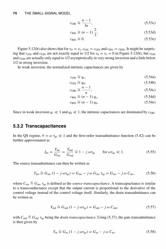
74 THE SMALL-SIGNAL MODEL
cGBi∼=
n − 1
3n, (5.53c)
cBSi∼= (n − 1)
2
3, (5.53d)
cBDi∼= 0. (5.53e)
Figure 5.12(b) also shows that for vd = vs, cGSi = cGDi and cBSi = cBDi. It might be surpris-
ing that cGSi and cGDi are not exactly equal to 1/2 for vd = vs = 0 in Figure 5.12(b), but cGSi
and cGDi are actually only equal to 1/2 asymptotically in very strong inversion and a little below
1/2 in strong inversion.
In weak inversion, the normalized intrinsic capacitances are given by
cGSi∼= qs, (5.54a)
cGDi∼= qd, (5.54b)
cGBi∼=
n − 1
n, (5.54c)
cBSi∼= (n − 1) qs, (5.54d)
cBDi∼= (n − 1) qd. (5.54e)
Since in weak inversion qs ≪ 1 and qd ≪ 1, the intrinsic capacitances are dominated by cGBi.
5.3.2 Transcapacitances
In the QS regime, θ = ω τqs ≪ 1 and the first-order transadmittance function (5.42) can be
further approximated as
ξm =Yms
Gms
=Ymd
Gmd
∼= 1 − j ωτqs for ωτqs ≪ 1. (5.55)
The source transadmittance can then be written as
Yms∼= Gms (1 − j ωτqs) = Gms − j ω Gms τqs = Gms − j ω Cms, (5.56)
where Cms Gms τqs is defined as the source transcapacitance. A transcapacitance is similar
to a transconductance except that the output current is proportional to the derivative of the
control voltage instead of the control voltage itself. Similarly, the drain transadmittance can
be written as
Ymd∼= Gmd (1 − j ωτqs) = Gmd − j ω Cmd, (5.57)
with Cmd Gmd τqs being the drain transcapacitance. Using (5.37), the gate transadmittance
is then given by
Ym∼= Gm (1 − j ωτqs) = Gm − j ω Cm, (5.58)
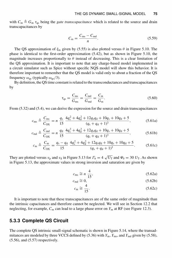
THE QS DYNAMIC SMALL-SIGNAL MODEL 75
with Cm Gm τqs being the gate transcapacitance which is related to the source and drain
transcapacitances by
Cm =Cms − Cmd
n. (5.59)
The QS approximation of ξm given by (5.55) is also plotted versus θ in Figure 5.10. The
phase is identical to the first-order approximation (5.42), but as shown in Figure 5.10, the
magnitude increases proportionally to θ instead of decreasing. This is a clear limitation of
the QS approximation. It is important to note that any charge-based model implemented in
a circuit simulator such as Spice without specific NQS model will show this behavior. It is
therefore important to remember that the QS model is valid only to about a fraction of the QS
frequency ωqs (typically ωqs/3).
By definition, the QS time constant is related to the transconductances and transcapacitances
by
τqs =Cms
Gms
=Cmd
Gmd
=Cm
Gm
. (5.60)
From (5.32) and (5.4), we can derive the expression for the source and drain transcapacitances
cms Cms
COX
= nqs
15
4q2s + 4q2
d + 12qsqd + 10qs + 10qd + 5
(qs + qd + 1)3, (5.61a)
cmd Cmd
COX
= nqd
15
4q2s + 4q2
d + 12qsqd + 10qs + 10qd + 5
(qs + qd + 1)3, (5.61b)
cm Cm
COX
=qs − qd
15
4q2s + 4q2
d + 12qsqd + 10qs + 10qd + 5
(qs + qd + 1)3. (5.61c)
They are plotted versus vp and vd in Figure 5.13 for Γb = 4√
UT and Ψ0 = 30 UT. As shown
in Figure 5.13, the approximate values in strong inversion and saturation are given by
cms∼= n
4
15, (5.62a)
cmd∼= 0, (5.62b)
cm∼=
4
15. (5.62c)
It is important to note that these transcapacitances are of the same order of magnitude than
the intrinsic capacitances and therefore cannot be neglected. We will see in Section 12.2 that
neglecting, for example, Cm can lead to a large phase error on Ym at RF (see Figure 12.3).
5.3.3 Complete QS Circuit
The complete QS intrinsic small-signal schematic is shown in Figure 5.14, where the transad-
mitances are modeled by three VCCS defined by (5.36) with Ym, Yms, and Ymd given by (5.58),
(5.56), and (5.57) respectively.
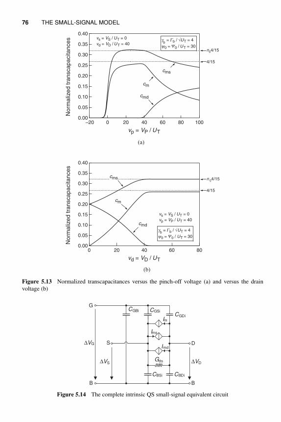
76 THE SMALL-SIGNAL MODEL
0.40
0.35
0.30
0.25
0.20
0.15
0.10
0.05
0.00
Norm
aliz
ed tra
nscapacitances
100806040200–20
vp = VP / UT
gb = Gb / √UT = 4
y0 = Y0 / UT = 30
vs = VS / UT = 0
vd = VD / UT = 40
cms
cm
cmd
n04/15
4/15
(a)
(b)
0.40
0.35
0.30
0.25
0.20
0.15
0.10
0.05
0.00
Norm
aliz
ed tra
nscapacitances
806040200
vd = VD / UT
gb = Gb / √UT = 4
y0 = Y0 / UT = 30
vs = VS / UT = 0
vp = VP / UT = 40
cms
cmd
cm
n 04/15
4/15
Figure 5.13 Normalized transcapacitances versus the pinch-off voltage (a) and versus the drain
voltage (b)
Im
Ims
Imd
Gds
GCGSi
CGDi
CGBi
CBSi CBDi
D
BB
S∆VG
∆VS ∆VD
Figure 5.14 The complete intrinsic QS small-signal equivalent circuit
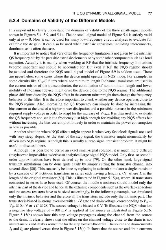
THE QS DYNAMIC SMALL-SIGNAL MODEL 77
5.3.4 Domains of Validity of the Different Models
It is important to clearly understand the domains of validity of the three small-signal models
shown in Figures 5.4, 5.9, and 5.14. The dc small-signal model of Figure 5.4 is strictly valid
only at ω = 0. Now it can be used for many low-frequency circuit analyses to evaluate for
example the dc gain. It can also be used when extrinsic capacitors, including interconnects,
dominate, as is often the case.
It is important to notice that very often the frequency limitation is not given by the intrinsic
QS frequency but by the parasitic extrinsic elements or by some other component such as a load
capacitor. Actually it is mainly when working at RF that the intrinsic frequency limitations
become important and should be accounted for. But even at RF, the NQS regime should
be avoided and therefore the NQS small-signal model of Figure 5.9 is seldom used. There
are nevertheless some cases where the device might operate in NQS mode. For example, in
some circuits like Gm-C filters where nonminimum length P-channel transistors are used in
the current mirror of the transconductor, the combination of nonminimum length and lower
mobility of P-channel device might drive the device close to the NQS regime. The additional
phase shift introduced by the NQS effect in the current mirror might then change the frequency
behavior of the filter. It is therefore important to check whether any device operates close to
the NQS regime. Also, increasing the QS frequency can simply be done by increasing the
bias current at the cost of a higher power dissipation and a possible increase in the minimum
required supply voltage in order to adapt for the increase of VDSsat. It is then useful to evaluate
the QS frequency and set it at a frequency just high enough for avoiding any NQS effects but
without increasing the bias current prohibitively in order to maintain the power consumption
as low as possible.
Another situation where NQS effects might appear is when very fast clock signals are used
with very steep slopes. At the start of the step signal, the transistor might momentarily be
driven into NQS regime. Although this is usually a large-signal transient problem, it might be
useful to discuss it here.
Although it is possible to derive an exact small-signal solution, it is much more difficult
(maybe even impossible) to derive an analytical large-signal NQS model. Only first- or second-
order approximations have been derived up to now [79]. On the other hand, large-signal
transient simulations can be done quite easily by simply cutting the transistor channel into
several slices [80]. This can easily be done by replacing in a circuit simulator a single transistor
by a cascade of N fictitious transistors in series each having a length L/N , where L is the
length of the original transistor [80]. This is illustrated in Figure 5.15(a), where 10 transistors
connected in series have been used. Of course, the middle transistors should model only the
intrinsic part of the device and hence all the extrinsic components such as the overlap capacitors
and the access resistors have to be sized accordingly. In the following example, we simulated
only the intrinsic behavior and therefore all the transistors include only the intrinsic part. The
transistor is biased in strong inversion with a 1-V gate and drain voltage, corresponding to VG −VT0
∼= 0.4 V or I C ∼= 28. The source voltage is biased at 0 V. To illustrate the NQS behavior,
a negative step voltage of −100 mV is applied at the source as illustrated in Figure 5.16.
Figure 5.15(b) shows how this step voltage propagates along the channel from the source
to the drain. It clearly shows that the effect on the channel voltage close to the drain is not
instantaneous and it takes some time for the step to reach the drain. The source and drain currents
IS and ID are plotted versus time in Figure 5.15(c). It shows that the source and drain currents
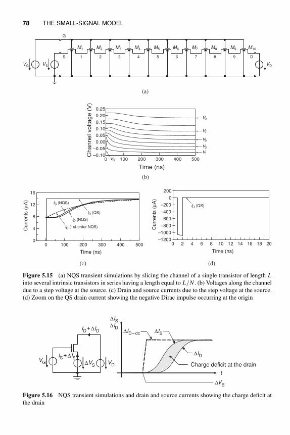
78 THE SMALL-SIGNAL MODEL
M2 M3 M4M1 M5 M7 M8 M9M6 M10
1 2 3 4 5 6 7 8 9
VSVG VD
D
G
S
0.25
0.20
0.15
0.10
0.05
0.00
–0.05
–0.10Channel voltage (
V)
5004003002001000
Time (ns)
VS
V1
V3
V5
V7
V9
(a)
(b)
(c) (d)
16
12
8
4
0
Cu
rre
nts
(µ
A)
5004003002001000
Time (ns)
ID (NQS)
IS (NQS)
ID (1st-order NQS)
ID (QS)
–1200
–1000
–800
–600
–400
–200
0
200
Cu
rre
nts
(µ
A)
20181614121086420
Time (ns)
ID (QS)
Figure 5.15 (a) NQS transient simulations by slicing the channel of a single transistor of length L
into several intrinsic transistors in series having a length equal to L/N . (b) Voltages along the channel
due to a step voltage at the source. (c) Drain and source currents due to the step voltage at the source.
(d) Zoom on the QS drain current showing the negative Dirac impulse occurring at the origin
t
Charge deficit at the drainV
V
V DVG
II
I I
I
II I
I
Figure 5.16 NQS transient simulations and drain and source currents showing the charge deficit at
the drain
THE QS DYNAMIC SMALL-SIGNAL MODEL 79
are not equal and that the drain current lags the source current. This situation is reproduced
in a slightly larger scale in Figure 5.16. Note that the area between the source current (top
curve) and the drain current (lower curve) represents charges that actually never reach the drain
and therefore constitutes a charge deficit at the drain.
The result obtained from the QS model of a single transistor with the same total length
and bias is also plotted in Figure 5.15(c). As expected from the expression of the source
transadmittance (5.56), the response to this step voltage is a large negative peak (actually a
Dirac impulse) corresponding to the derivative of the input voltage due to the transcapacitance
part of the source transadmittance, followed by an instantaneous change of the drain current
due to the transconductance part of the source transadmittance. Since the QS model ensures
charge conservation, the negative spike represents the charge deficit at the drain observed in the
NQS simulations but these charges are actually taken away from the drain current immediately
instead of not reaching the drain as is the case in the NQS simulation. This is illustrated in
Figure 5.15(d), where the QS drain current ID(QS) shown in Figure 5.15(c) has been zoomed
out to show the negative impulse. Notice the large value of the negative impulse amplitude
which in some cases may give rise to simulation (convergence) problems.
Also plotted in Figure 5.15(c) is the result obtained from the time domain equivalent of the
first-order NQS approximation given by (5.42). As expected it differs from the NQS simulation
at small time values but then follows quite nicely the NQS simulation after about 150 ns. The
major difference with the QS simulation is that the spike has now disappeared, avoiding any
simulation problems. Note that the second-order NQS approximation would of course give an
even better result.

6 The Noise Model
This chapter is dedicated to the modeling of the noise in the MOS transistor focusing mainly on
the intrinsic part and assuming that the device has a long channel and hence does not account
for short-channel effects which are described in Section 9.4. There are mainly two kinds of
noises coming from the channel region, namely the thermal noise and the flicker or 1/ f noise.
Both can be described by a local noise source which depends on the position along the channel.
Section 6.1 shortly presents the different methods to calculate the power spectral density (PSD)
of the drain current fluctuations, by integration of the local noise source along the channel. The
method will then be applied for both the thermal noise and the flicker noise. The low-frequency
thermal noise is then derived in Section 6.2. The thermal noise parameter is defined as the ratio
of the drain thermal noise conductance to the output conductance at VD = VS (or equivalently
the source transconductance), and the thermal excess noise factor is the ratio of the drain
thermal noise conductance and the gate transconductance. The use of these two parameters is
illustrated by several circuit examples. Section 6.3 is devoted to flicker noise, which arises from
several sources: the fluctuation of the number of mobile carriers in the channel, discussed in
Section 6.3.1, the fluctuation of the mobility, presented in Section 6.3.2, and finally the flicker
noise coming from the access resistances, described in Section 6.3.3. The bias dependence of
all the three noise sources is particularly emphasized. All three contributions are compared
in Section 6.3.4 using measured data from the literature. Finally, the scaling properties of the
flicker noise are discussed in Section 6.3.5.
6.1 NOISE CALCULATION METHODS
6.1.1 General Expression
The origin of noise is related to local random fluctuations of the carrier velocity or the carrier
density. These local fluctuations can be modeled by adding a random current to the local dc
current as shown in Figure 6.1(a). They then propagate to the terminals resulting in fluctuations
of the voltages or currents around the dc operating point. There are clearly two different parts in
the noise analysis: the microscopic part which consists in deriving the statistics of the stochastic
Charge-Based MOS Transistor Modeling: The EKV Model for Low-Power and RF IC Design C. Enz and E. VittozC© 2006 John Wiley & Sons, Ltd.
0 Lx
0 L
x
δInD
δIn (
DS
∆InDDS
δIn
δVn
0 L
x
δID
δ
δ
Ix
DS
(b)
(c)
(d)
x
x
x + ∆xx
0 L
x
δInD
δIx
DS
(e)
x + ∆xx
lx
0 L
x
∆InDDS
δIn(x, t )
δVn (x, t)
(a)
x
G
(x, t)
(x, t )
x, t )
Figure 6.1 Equivalent circuits of the MOS transistor noisy channel illustrating different noise analysis
approaches. (a) The Langevin method used by Klassen and Prins [81], where a distributed noise
source is added to the differential equation giving the drain current. (b) Circuit obtained from (a) after
linearization of the differential equation and keeping only the first-order terms. (c) Equivalent small-
signal circuit approach: since the circuit of (b) is linear, the effect of each local noise source on the
drain current fluctuation can be calculated separately and summed at the drain. (d) The impedance field
method, where the current response δID at the drain due to a current δIx injected at position x along
channel and the corresponding current Ai(x) δID/δIx are calculated. The noise is then evaluated
from the derivative of Ai(x) with respect to x
NOISE CALCULATION METHODS 83
process such as the velocity fluctuation and translating it into a variation of the local current,
and the macroscopic part which consists in calculating the response of the terminal currents
(or voltages) to these fluctuations or in other words how these local fluctuations propagate
to the terminals and produce variations of the terminal voltages or currents. In this part we
will mainly focus on the macroscopic part, namely finding a common expression for the PSD
of the drain current fluctuations due to all the microscopic local noise sources located in the
channel. At this stage, it is important to point out that these local fluctuations are always small
and consequently, the analysis of the propagation of the noise sources to the terminal voltages
or currents reduces to a linear analysis. Hence, the principle of superposition can be applied
for adding the effects of all the noise sources along the channel. In principle, since these noise
sources are random process, they might be spatially correlated, which should be accounted for
when summing their effects. However, in all of the cases discussed below, it will be assumed
that the local sources are spatially uncorrelated and therefore their PSD can be summed.
Several methods have been used for the calculation of noise in the MOS transistor. A de-
tailed description of all these different methods goes beyond the objective of this book, but they
will be briefly illustrated below. The first approach is based on the Langevin method and was
used by Klaassen and Prins [81] initially for deriving the thermal noise and was then extended
by Klaassen to also account for the flicker noise [82] and by Langevelde to include also the
induced gate noise [83]. It starts with the differential equation giving the drain current (4.5), to
which a Langevin noise source δIn(x, t) is added as shown in Figure 6.1(a). This distributed
noise source depends on the position along the channel and induce channel voltage fluctuations
δVn(x, t) that should normally be accounted for if the δIn(x, t) would be large-signal fluctu-
ations. Since these voltage fluctuations are much smaller than the thermodynamic voltage, the
current differential equation can be linearized, resulting in the equivalent small-signal circuit
shown in Figure 6.1(b). Since this equivalent circuit is now linear, the superposition principle
can be used. The problem can then be reduced to isolating a single noise source in the
channel and calculate its effect δInD on the drain terminal current as shown in Figure 6.1(c).
The total effect is then obtained by summing the contributions of all the noise sources along
the channel assuming they are spatially uncorrelated. This latter approach will be called the
equivalent small-signal circuit approach.1 Note that a similar transmission line approach has
also been used [84]. A third approach is the impedance field method (IFM) initially introduced
by Shockley [85] and modified afterward by van Vliet [86,87]. As illustrated in Figure 6.1(d),
the channel is excited by a current δIx at position x along the channel, and the current response
δID at the drain terminal and the corresponding current gain Ai(x)∆δID/δIx are calculated. The
noise due to the local noise source at position x is then evaluated from the so-called impedance
field2 corresponding to the derivative of the current gain with respect to x at each position.
Taking the derivative with respect to position corresponds actually to taking the difference
between the current gain at positions x + ∆x and x , which is illustrated in Figure 6.1(e). If δIx
is set equal to the local noise source δIn(x), then the equivalent circuit of Figure 6.1(e) reduces
to the circuit of Figure 6.1(c). The IFM is therefore equivalent to the small-signal circuit
approach. A more rigorous demonstration shows that actually the three approaches mentioned
above are equivalent [156].
1 It is sometimes also called the two-transistor approach.2 The name impedance field comes from the fact that the terminal voltage fluctuations were initially evaluated resulting
in a gain between the excitation current and the voltage fluctuation that has the dimension of an impedance (it is actually
a transimpedance).
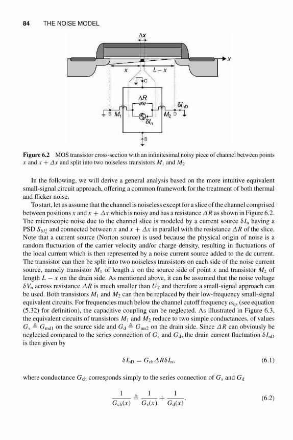
84 THE NOISE MODEL
Figure 6.2 MOS transistor cross-section with an infinitesimal noisy piece of channel between points
x and x + ∆x and split into two noiseless transistors M1 and M2
In the following, we will derive a general analysis based on the more intuitive equivalent
small-signal circuit approach, offering a common framework for the treatment of both thermal
and flicker noise.
To start, let us assume that the channel is noiseless except for a slice of the channel comprised
between positions x and x + ∆x which is noisy and has a resistance ∆R as shown in Figure 6.2.
The microscopic noise due to the channel slice is modeled by a current source δIn having a
PSD SδI 2n
and connected between x and x + ∆x in parallel with the resistance ∆R of the slice.
Note that a current source (Norton source) is used because the physical origin of noise is a
random fluctuation of the carrier velocity and/or charge density, resulting in fluctuations of
the local current which is then represented by a noise current source added to the dc current.
The transistor can then be split into two noiseless transistors on each side of the noise current
source, namely transistor M1 of length x on the source side of point x and transistor M2 of
length L − x on the drain side. As mentioned above, it can be assumed that the noise voltage
δVn across resistance ∆R is much smaller than UT and therefore a small-signal approach can
be used. Both transistors M1 and M2 can then be replaced by their low-frequency small-signal
equivalent circuits. For frequencies much below the channel cutoff frequency ωqs (see equation
(5.32) for definition), the capacitive coupling can be neglected. As illustrated in Figure 6.3,
the equivalent circuits of transistors M1 and M2 reduce to two simple conductances, of values
Gs Gmd1 on the source side and Gd Gms2 on the drain side. Since ∆R can obviously be
neglected compared to the series connection of Gs and Gd, the drain current fluctuation δInD
is then given by
δInD = Gch∆RδIn, (6.1)
where conductance Gch corresponds simply to the series connection of Gs and Gd
1
Gch(x)
1
Gs(x)+
1
Gd(x). (6.2)
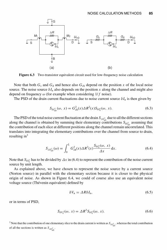
NOISE CALCULATION METHODS 85
δInD
δIn
∆RM1 M2
G
B
DS
(a)
δInD
δIn
∆R
DS
Gs Gd
(b)
Figure 6.3 Two-transistor equivalent circuit used for low-frequency noise calculation
Note that both Gs and Gd and hence also Gch depend on the position x of the local noise
source. The noise source δIn also depends on the position x along the channel and might also
depend on frequency ω (for example when considering 1/ f noise).
The PSD of the drain current fluctuations due to noise current source δIn is then given by
SδI 2nD
(ω, x) = G2ch(x)∆R2(x)SδI 2
n(ω, x). (6.3)
The PSD of the total noise current fluctuation at the drain S∆I 2nD
due to all the different sections
along the channel is obtained by summing their elementary contributions SδI 2nD
assuming that
the contribution of each slice at different positions along the channel remain uncorrelated. This
translates into integrating the elementary contributions over the channel from source to drain,
resulting in3
S∆I 2nD
(ω) =∫ L
0
G2ch(x)∆R2(x)
SδI 2n(ω, x)
∆xdx . (6.4)
Note that SδI 2n
has to be divided by ∆x in (6.4) to represent the contribution of the noise current
source by unit length.
As explained above, we have chosen to represent the noise source by a current source
(Norton source) in parallel with the elementary section because it is closer to the physical
origin of noise. As shown in Figure 6.4, we could of course also use an equivalent noise
voltage source (Thevenin equivalent) defined by
δVn = ∆RδIn, (6.5)
or in terms of PSD,
SδV 2n(ω, x) = ∆R2SδI 2
n(ω, x). (6.6)
3 Note that the contribution of one elementary slice to the drain current is written as SδI 2
nD, whereas the total contribution
of all the sections is written as S∆I 2nD
.
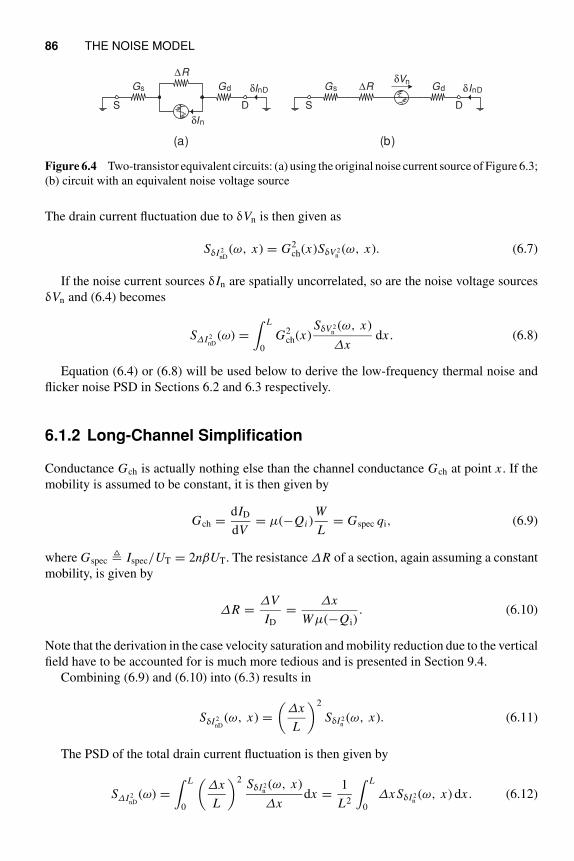
86 THE NOISE MODEL
δInD∆R
DS
Gs GdδVn
δInD
δIn
∆R
DS
Gs Gd
(a) (b)
Figure 6.4 Two-transistor equivalent circuits: (a) using the original noise current source of Figure 6.3;
(b) circuit with an equivalent noise voltage source
The drain current fluctuation due to δVn is then given as
SδI 2nD
(ω, x) = G2ch(x)SδV 2
n(ω, x). (6.7)
If the noise current sources δIn are spatially uncorrelated, so are the noise voltage sources
δVn and (6.4) becomes
S∆I 2nD
(ω) =∫ L
0
G2ch(x)
SδV 2n(ω, x)
∆xdx . (6.8)
Equation (6.4) or (6.8) will be used below to derive the low-frequency thermal noise and
flicker noise PSD in Sections 6.2 and 6.3 respectively.
6.1.2 Long-Channel Simplification
Conductance Gch is actually nothing else than the channel conductance Gch at point x . If the
mobility is assumed to be constant, it is then given by
Gch =dID
dV= µ(−Qi )
W
L= Gspec qi, (6.9)
where Gspec Ispec/UT = 2nβUT. The resistance ∆R of a section, again assuming a constant
mobility, is given by
∆R =∆V
ID
=∆x
Wµ(−Qi). (6.10)
Note that the derivation in the case velocity saturation and mobility reduction due to the vertical
field have to be accounted for is much more tedious and is presented in Section 9.4.
Combining (6.9) and (6.10) into (6.3) results in
SδI 2nD
(ω, x) =(
∆x
L
)2
SδI 2n(ω, x). (6.11)
The PSD of the total drain current fluctuation is then given by
S∆I 2nD
(ω) =∫ L
0
(∆x
L
)2 SδI 2n(ω, x)
∆xdx =
1
L2
∫ L
0
∆x SδI 2n(ω, x) dx . (6.12)
LOW-FREQUENCY CHANNEL THERMAL NOISE 87
A more formal derivation of (6.12) is given in Appendix A2 at the end of this chapter,
following the approach of Klaassen and Prins [81]. Note that the above model ignored the
capacitive coupling of the noise generated in the channel to the gate. The latter will be analyzed
in the high-frequency noise model described in Chapter 13.
6.2 LOW-FREQUENCY CHANNEL THERMAL NOISE
6.2.1 Drain Current Thermal Noise PSD
The PSD of the drain current fluctuations due to thermal noise in the channel can be evaluated
using (6.4) or (6.8). The PSD of the noise current source of one section is then simply given
from (6.10):
SδI 2n
=4kT
∆R= 4kT
Wµ(−Qi)
∆x, (6.13)
where k is the Boltzmann constant and T is the absolute temperature.
The PSD of the total drain current fluctuation S∆I 2nD
is obtained from (6.12) as
S∆I 2nD
4kT · GnD = 4kT1
L2
∫ L
0
Wµ[−Qi(x)] dx
= 4kT µW
L2
∫ L
0
[−Qi(x)] dx,
(6.14)
where it has been assumed that the mobility µ is constant. The thermal noise conductance at
the drain GnD is then defined as
GnD µW
L2
∫ L
0
[−Qi(x)] dx =µ
L2|QI|, (6.15)
where QI is the total inversion charge in the channel given by
QI W
∫ L
0
Qi(x) dx . (6.16)
Hence, for a mobility that is independent of the electric field, the noise conductance is propor-
tional to the total inversion charge “stored” in the channel. Equation (6.15) can be written in
normalized form as
gnD GnD
Gspec
=∫ 1
0
qi(ξ ) · dξ = qI QI
Qspec
. (6.17)
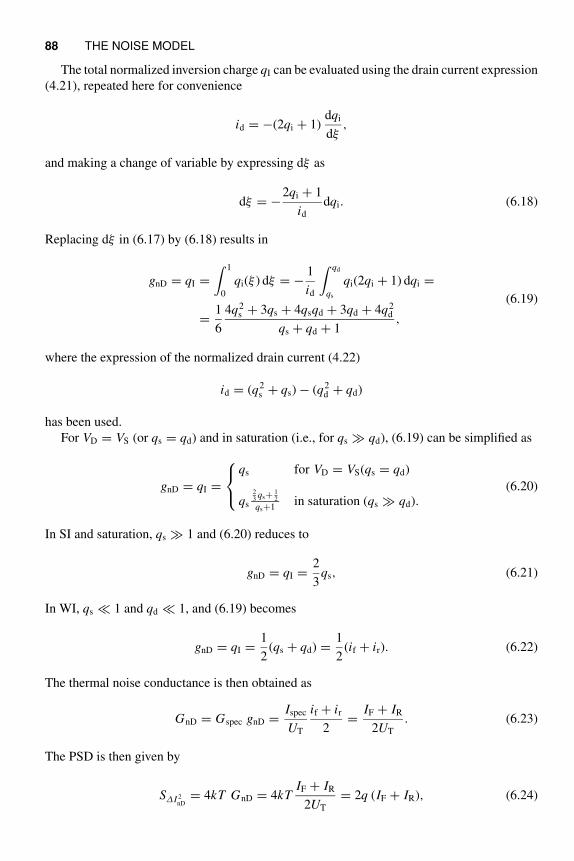
88 THE NOISE MODEL
The total normalized inversion charge qI can be evaluated using the drain current expression
(4.21), repeated here for convenience
id = −(2qi + 1)dqi
dξ,
and making a change of variable by expressing dξ as
dξ = −2qi + 1
id
dqi. (6.18)
Replacing dξ in (6.17) by (6.18) results in
gnD = qI =∫ 1
0
qi(ξ ) dξ = −1
id
∫ qd
qs
qi(2qi + 1) dqi =
=1
6
4q2s + 3qs + 4qsqd + 3qd + 4q2
d
qs + qd + 1,
(6.19)
where the expression of the normalized drain current (4.22)
id = (q2s + qs) − (q2
d + qd)
has been used.
For VD = VS (or qs = qd) and in saturation (i.e., for qs ≫ qd), (6.19) can be simplified as
gnD = qI =
⎧⎨⎩
qs for VD = VS(qs = qd)
qs
23
qs+ 12
qs+1in saturation (qs ≫ qd).
(6.20)
In SI and saturation, qs ≫ 1 and (6.20) reduces to
gnD = qI =2
3qs, (6.21)
In WI, qs ≪ 1 and qd ≪ 1, and (6.19) becomes
gnD = qI =1
2(qs + qd) =
1
2(if + ir). (6.22)
The thermal noise conductance is then obtained as
GnD = Gspec gnD =Ispec
UT
if + ir
2=
IF + IR
2UT
. (6.23)
The PSD is then given by
S∆I 2nD
= 4kT GnD = 4kTIF + IR
2UT
= 2q (IF + IR), (6.24)
LOW-FREQUENCY CHANNEL THERMAL NOISE 89
ID
D
B
S
G
∆InD
Noiseless
ID + ∆InD
D
B
S
G
Noisy
(a) (b)
Figure 6.5 Thermal noise equivalent circuit with noiseless transistor
which corresponds to full shot noise of both the forward and the reverse components of the drain
current [88]. This result might be surprising since the above derivation used the expression of
the local thermal noise and integrated its effect on the drain current over the channel. In weak
inversion the current is dominated by diffusion and, similar to a bipolar transistor, the noise
can be interpreted as shot noise related to the potential barriers at the source and the drain.
Nevertheless, it can be shown that expression (6.15) (or its normalized form (6.17)), which
was derived with the assumptions of thermal noise due to the channel conductance, is valid in
all regions of inversion [89, 90].
Assuming that the channel thermal noise is the only source of noise within the transistor,
for frequencies much below the channel cutoff frequency ωqs, the noisy transistor can then
be modeled as a noiseless device to which a noisy current source ∆InD is connected between
drain and source as shown in Figure 6.5. This noisy current source has a PSD given by (6.14),
where the noise conductance GnD is given by
GnD = Gspec qI, (6.25)
where qI is given by (6.19).
6.2.2 Thermal Noise Excess Factor Definitions
Several thermal noise excess factors can be defined according to the definitions introduced
initially by van der Ziel [91]. The thermal noise parameter related to the drain terminal δnD is
defined as4
δnD GnD
Gds0
, (6.26)
where Gds0 is the drain-to-source conductance at VDS = 0,
Gds0 = Gms = Gspec qs. (6.27)
4 Van der Ziel initially used γ for the thermal noise parameter defined by (6.26) and α for the noise excess factor
defined by (6.30). The most important noise excess factor from a circuit design point of view is the one given by
(6.30), which has been called γ in many papers instead of α as it was defined initially by Van der Ziel [91]. We will
keep the circuit design definition of γ and rename the Van der Ziel’s γ as δ.
90 THE NOISE MODEL
The δnD parameter shows how much the thermal noise of the active device deviates from
the value it takes when it operates as a passive resistor of conductance Gds0. Since for VDS = 0
the noise conductance GnD is equal to the channel conductance Gds0, the noise parameter δnD
is then equal to unity.
Assuming constant mobility, (6.25) can be used together with (6.27) in (6.26), allowing δnD
to be written in terms of the normalized charges as
δnD =qI
qs
. (6.28)
In saturation, from (6.20), δnD is equal to
δnD =2
3
qs + 3/4
qs + 1=
1/2 WI and saturation (qs ≪ 1)
2/3 SI and saturation (qs ≫ 1).(6.29)
Note that the δnD thermal noise parameter compares the thermal noise conductance evaluated
at a given operating point that is not necessarily the same as the one used to define the output
conductance Gds0 (i.e., VDS = 0). It is therefore not very useful for circuit design and is used
more for modeling purposes.
For circuit design, it is more useful to define another figure of merit, γnD, named the thermal
noise excess factor related to the drain and defined as
γnD GnD
Gm
=gnD
gm
=nqI
qs − qd
. (6.30)
γnD represents how much noise is generated at the drain of a transistor for a given gate transcon-
ductance. Contrary to the δnD thermal noise parameter, the noise conductance and the gate
transconductance used in the definition (6.30) are evaluated at the same operating point. γnD
has a direct impact on the noise performance of circuits.
The smaller γnD, the better the noise performance of the device. Note that γnD can become
quite large in the linear region when VD tends to VS. Indeed, in this region, the gate transconduc-
tance gets smaller as the drain-to-source voltage decreases, but the thermal noise conductance
does not decrease, resulting in a degradation of the γnD noise excess factor. At the limit when
VD becomes equal to VS, the gate transconductance becomes zero and γnD tends to infinity.
Note that γnD is also a figure of merit that can be used for any transconductor (even for circuit
transconductors) to evaluate how much thermal noise is generated for a given transconductance.
The smaller γnD, the better the transconductor.
The δnD thermal noise parameter and the γnD noise excess factor are related by
γnD =GnD
Gds0
Gds0
Gm
= δnD
Gds0
Gm
= δnD nGds0
Gms − Gmd
= δnD nqs
qs − qd
. (6.31)
In saturation, Gmd = 0 and qd = 0, resulting in
γnD = δnD nGds0
Gms
= δnD n =
n2
WI and saturation
n 23
SI and saturation,(6.32)
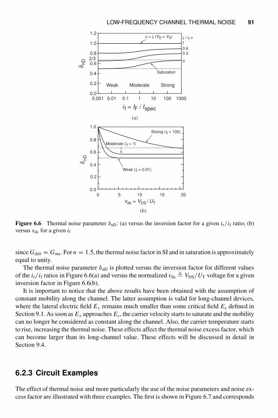
LOW-FREQUENCY CHANNEL THERMAL NOISE 91
1.2
1.0
0.8
0.6
0.4
0.2
0.0
δn
D
0.001 0.01 0.1 1 10 100 1000
i f = IF / Ispec
Moderate StrongWeak
2/3
if = ir (VD = VS)
Saturation
ir / i f =
1
0
0.3
0.6
(a)
(b)
1.0
0.8
0.6
0.4
0.2
0.0
δnD
20151050
vds = VDS / UT
Strong (if = 100)
Moderate (i f = 1)
Weak (if = 0.01)
Figure 6.6 Thermal noise parameter δnD: (a) versus the inversion factor for a given ir/ if ratio; (b)
versus vds for a given if
since Gds0 = Gms. For n = 1.5, the thermal noise factor in SI and in saturation is approximately
equal to unity.
The thermal noise parameter δnD is plotted versus the inversion factor for different values
of the ir/ if ratios in Figure 6.6(a) and versus the normalized vds VDS/UT voltage for a given
inversion factor in Figure 6.6(b).
It is important to notice that the above results have been obtained with the assumption of
constant mobility along the channel. The latter assumption is valid for long-channel devices,
where the lateral electric field Ex remains much smaller than some critical field Ec defined in
Section 9.1. As soon as Ex approaches Ec, the carrier velocity starts to saturate and the mobility
can no longer be considered as constant along the channel. Also, the carrier temperature starts
to rise, increasing the thermal noise. These effects affect the thermal noise excess factor, which
can become larger than its long-channel value. These effects will be discussed in detail in
Section 9.4.
6.2.3 Circuit Examples
The effect of thermal noise and more particularly the use of the noise parameters and noise ex-
cess factor are illustrated with three examples. The first is shown in Figure 6.7 and corresponds
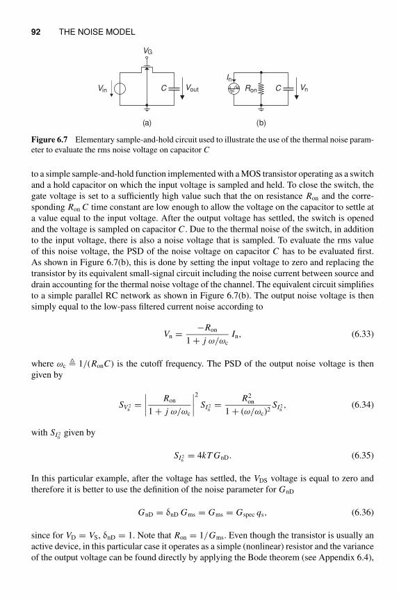
92 THE NOISE MODEL
C RonVin Vout
VG
C Vn
In
(a) (b)
Figure 6.7 Elementary sample-and-hold circuit used to illustrate the use of the thermal noise param-
eter to evaluate the rms noise voltage on capacitor C
to a simple sample-and-hold function implemented with a MOS transistor operating as a switch
and a hold capacitor on which the input voltage is sampled and held. To close the switch, the
gate voltage is set to a sufficiently high value such that the on resistance Ron and the corre-
sponding Ron C time constant are low enough to allow the voltage on the capacitor to settle at
a value equal to the input voltage. After the output voltage has settled, the switch is opened
and the voltage is sampled on capacitor C . Due to the thermal noise of the switch, in addition
to the input voltage, there is also a noise voltage that is sampled. To evaluate the rms value
of this noise voltage, the PSD of the noise voltage on capacitor C has to be evaluated first.
As shown in Figure 6.7(b), this is done by setting the input voltage to zero and replacing the
transistor by its equivalent small-signal circuit including the noise current between source and
drain accounting for the thermal noise voltage of the channel. The equivalent circuit simplifies
to a simple parallel RC network as shown in Figure 6.7(b). The output noise voltage is then
simply equal to the low-pass filtered current noise according to
Vn =−Ron
1 + j ω/ωc
In, (6.33)
where ωc 1/(RonC) is the cutoff frequency. The PSD of the output noise voltage is then
given by
SV 2n
=∣∣∣∣
Ron
1 + j ω/ωc
∣∣∣∣2
SI 2n
=R2
on
1 + (ω/ωc)2SI 2
n, (6.34)
with SI 2n
given by
SI 2n
= 4kT GnD. (6.35)
In this particular example, after the voltage has settled, the VDS voltage is equal to zero and
therefore it is better to use the definition of the noise parameter for GnD
GnD = δnD Gms = Gms = Gspec qs, (6.36)
since for VD = VS, δnD = 1. Note that Ron = 1/Gms. Even though the transistor is usually an
active device, in this particular case it operates as a simple (nonlinear) resistor and the variance
of the output voltage can be found directly by applying the Bode theorem (see Appendix 6.4),
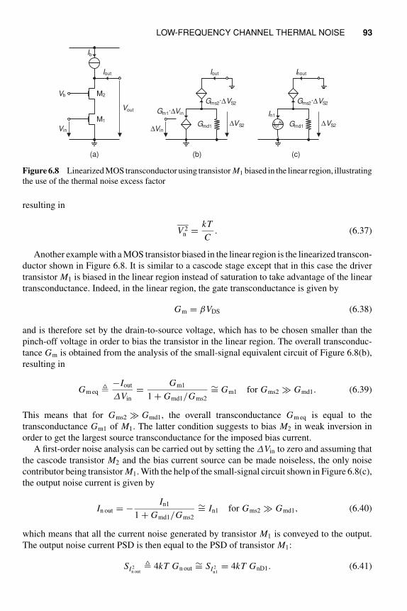
LOW-FREQUENCY CHANNEL THERMAL NOISE 93
M1
M2
Ib
Iout
Vin
Vout
Vb
Gm1·∆Vin
Gmd1
Gms2·∆VS2
Iout
∆Vin
∆VS2 Gmd1
Gms2·∆VS2
Inout
∆VS2
In1
(a) (b) (c)
Figure 6.8 Linearized MOS transconductor using transistor M1 biased in the linear region, illustrating
the use of the thermal noise excess factor
resulting in
V 2n =
kT
C. (6.37)
Another example with a MOS transistor biased in the linear region is the linearized transcon-
ductor shown in Figure 6.8. It is similar to a cascode stage except that in this case the driver
transistor M1 is biased in the linear region instead of saturation to take advantage of the linear
transconductance. Indeed, in the linear region, the gate transconductance is given by
Gm = βVDS (6.38)
and is therefore set by the drain-to-source voltage, which has to be chosen smaller than the
pinch-off voltage in order to bias the transistor in the linear region. The overall transconduc-
tance Gm is obtained from the analysis of the small-signal equivalent circuit of Figure 6.8(b),
resulting in
Gm eq −Iout
∆Vin
=Gm1
1 + Gmd1/Gms2
∼= Gm1 for Gms2 ≫ Gmd1. (6.39)
This means that for Gms2 ≫ Gmd1, the overall transconductance Gm eq is equal to the
transconductance Gm1 of M1. The latter condition suggests to bias M2 in weak inversion in
order to get the largest source transconductance for the imposed bias current.
A first-order noise analysis can be carried out by setting the ∆Vin to zero and assuming that
the cascode transistor M2 and the bias current source can be made noiseless, the only noise
contributor being transistor M1. With the help of the small-signal circuit shown in Figure 6.8(c),
the output noise current is given by
In out = −In1
1 + Gmd1/Gms2
∼= In1 for Gms2 ≫ Gmd1, (6.40)
which means that all the current noise generated by transistor M1 is conveyed to the output.
The output noise current PSD is then equal to the PSD of transistor M1:
SI 2n out
4kT Gn out∼= SI 2
n1= 4kT GnD1. (6.41)
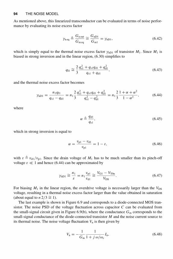
94 THE NOISE MODEL
As mentioned above, this linearized transconductor can be evaluated in terms of noise perfor-
mance by evaluating its noise excess factor
γn eq Gn out
Gm eq
∼=GnD1
Gm1
= γnD1, (6.42)
which is simply equal to the thermal noise excess factor γnD1 of transistor M1. Since M1 is
biased in strong inversion and in the linear region, (6.30) simplifies to
qI1∼=
2
3
q2s1 + qs1qd1 + q2
d1
qs1 + qd1
, (6.43)
and the thermal noise excess factor becomes
γnD1 =n1qI1
qs1 − qd1
= n1
2
3
q2s1 + qs1qd1 + q2
d1
q2s1 − q2
d1
= n1
2
3
1 + α + α2
1 − α2, (6.44)
where
α qd1
qs1
, (6.45)
which in strong inversion is equal to
α =vp1 − vd1
vp1
= 1 − ε, (6.46)
with ε vd1/vp1. Since the drain voltage of M1 has to be much smaller than its pinch-off
voltage ε ≪ 1 and hence (6.44) can be approximated by
γnD1∼=
n1
ε= n1
vp1
vd1
∼=VG1 − VT0n
VDS
. (6.47)
For biasing M1 in the linear region, the overdrive voltage is necessarily larger than the VDS
voltage, resulting in a thermal noise excess factor larger than the value obtained in saturation
(about equal to n 2/3 ∼= 1).
The last example is shown in Figure 6.9 and corresponds to a diode-connected MOS tran-
sistor. The noise PSD of the voltage fluctuation across capacitor C can be evaluated from
the small-signal circuit given in Figure 6.9(b), where the conductance Gm corresponds to the
small-signal conductance of the diode-connected transistor M and the noise current source to
its thermal noise. The noise voltage fluctuation Vn is then given by
Vn = −1
Gm
1
1 + j ω/ωc
In, (6.48)
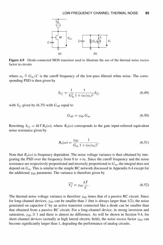
LOW-FREQUENCY CHANNEL THERMAL NOISE 95
M
Ib
C
Vout
(a) (b)
GmC Vn
In
Figure 6.9 Diode-connected MOS transistor used to illustrate the use of the thermal noise excess
factor in circuits
where ωc Gm/C is the cutoff frequency of the low-pass filtered white noise. The corre-
sponding PSD is then given by
SV 2n
=1
G2m
1
1 + (ω/ωc)2SI 2
n, (6.49)
with SI 2n
given by (6.35) with GnD equal to
GnD = γnD Gm. (6.50)
Rewriting SV 2n
= 4kT Rn(ω), where Rn(ω) corresponds to the gate input-referred equivalent
noise resistance given by
Rn(ω) =γnD
Gm
1
1 + (ω/ωc)2. (6.51)
Note that Rn(ω) is frequency dependent. The noise voltage variance is then obtained by inte-
grating the PSD over the frequency from 0 to +∞. Since the cutoff frequency and the noise
resistance are respectively proportional and inversely proportional to Gm, the integral does not
depend on Gm. This is similar to the simple RC network discussed in Appendix 6.4 except for
the additional γnD parameter. The variance is therefore given by
V 2n = γnD
kT
C. (6.52)
The thermal noise voltage variance is therefore γnD times that of a passive RC circuit. Since
for long-channel devices, γnD can be smaller than 1 (but is always larger than 1/2), the noise
generated on capacitor C by an active transistor connected like a diode can be smaller than
that obtained from a passive RC circuit. For a long-channel device, in strong inversion and
saturation, γnD∼= 1 and there is almost no difference. As will be shown in Section 9.4, for
short-channel devices (actually at high lateral electric field), the noise excess factor γnD can
become significantly larger than 1, degrading the performance of analog circuits.
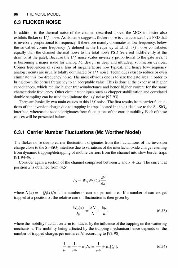
96 THE NOISE MODEL
6.3 FLICKER NOISE
In addition to the thermal noise of the channel described above, the MOS transistor also
exhibits flicker or 1/ f noise. As its name suggests, flicker noise is characterized by a PSD that
is inversely proportional to frequency. It therefore mainly dominates at low frequency, below
the so-called corner frequency fk defined as the frequency at which 1/ f noise contributes
equally than the channel thermal noise to the total noise PSD (referred indifferently at the
drain or at the gate). Because the 1/ f noise scales inversely proportional to the gate area, it
is becoming a major issue for analog I C design in deep and ultradeep submicron devices.
Corner frequencies of several tens of megahertz are now typical, and hence low-frequency
analog circuits are usually totally dominated by 1/ f noise. Techniques exist to reduce or even
eliminate this low-frequency noise. The most obvious one is to size the gate area in order to
bring down the corner frequency to an acceptable value. This is done at the expense of higher
capacitances, which require higher transconductance and hence higher current for the same
characteristic frequency. Other circuit techniques such as chopper stabilization and correlated
double sampling can be used to eliminate the 1/ f noise [92, 93].
There are basically two main causes to this 1/ f noise. The first results from carrier fluctua-
tions of the inversion charge due to trapping in traps located in the oxide close to the Si–SiO2
interface, whereas the second originates from fluctuations of the carrier mobility. Each of these
causes will be presented below.
6.3.1 Carrier Number Fluctuations (Mc Worther Model)
The flicker noise due to carrier fluctuations originates from the fluctuations of the inversion
charge close to the Si–SiO2 interface due to variations of the interfacial oxide charge resulting
from dynamic trapping/detrapping of mobile carriers from the channel into slow border traps
[91, 94–96].
Consider again a section of the channel comprised between x and x + ∆x . The current at
position x is obtained from (4.5)
ID = Wq N (x)µdV
dx,
where N (x) = −Qi(x)/q is the number of carriers per unit area. If a number of carriers get
trapped at a position x , the relative current fluctuation is then given by
δID(x)
ID
=δN
N+
δµ
µ, (6.53)
where the mobility fluctuation term is induced by the influence of the trapping on the scattering
mechanism. The mobility being affected by the trapping mechanism hence depends on the
number of trapped charges per unit area Nt according to [97, 98]
1
µ=
1
µ0
+ αc Nt =1
µ0
+ αc|Qt|, (6.54)
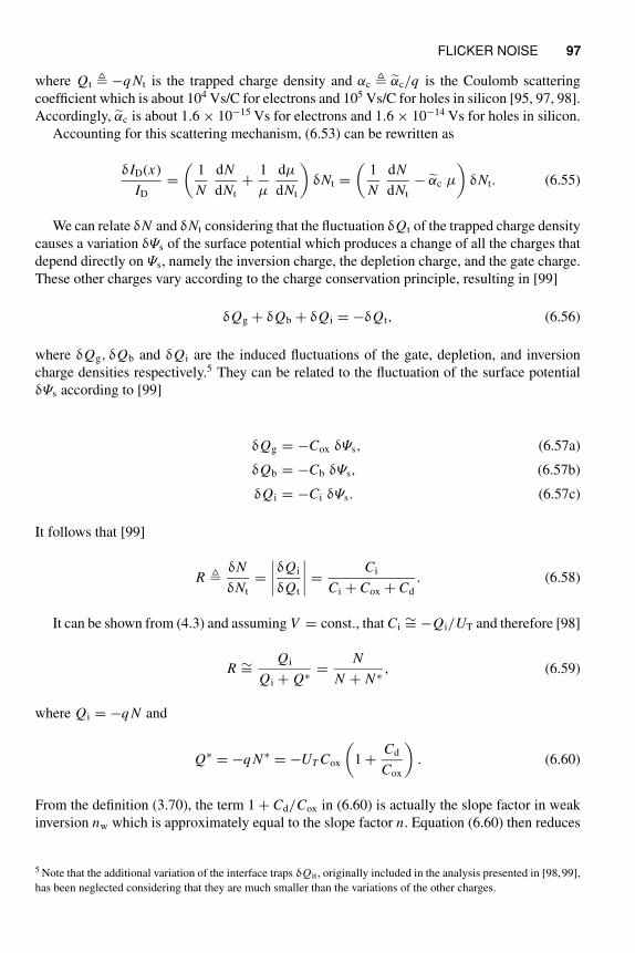
FLICKER NOISE 97
where Qt −q Nt is the trapped charge density and αc αc/q is the Coulomb scattering
coefficient which is about 104 Vs/C for electrons and 105 Vs/C for holes in silicon [95, 97, 98].
Accordingly, αc is about 1.6 × 10⁻¹⁵ Vs for electrons and 1.6 × 10⁻¹⁴ Vs for holes in silicon.
Accounting for this scattering mechanism, (6.53) can be rewritten as
δID(x)
ID
=(
1
N
dN
dNt
+1
µ
dµ
dNt
)δNt =
(1
N
dN
dNt
− αc µ
)δNt. (6.55)
We can relate δN and δNt considering that the fluctuation δQt of the trapped charge density
causes a variation δΨs of the surface potential which produces a change of all the charges that
depend directly on Ψs, namely the inversion charge, the depletion charge, and the gate charge.
These other charges vary according to the charge conservation principle, resulting in [99]
δQg + δQb + δQi = −δQt, (6.56)
where δQg, δQb and δQi are the induced fluctuations of the gate, depletion, and inversion
charge densities respectively.5 They can be related to the fluctuation of the surface potential
δΨs according to [99]
δQg = −Cox δΨs, (6.57a)
δQb = −Cb δΨs, (6.57b)
δQi = −Ci δΨs. (6.57c)
It follows that [99]
R δN
δNt
=∣∣∣∣δQi
δQt
∣∣∣∣ =Ci
Ci + Cox + Cd
. (6.58)
It can be shown from (4.3) and assuming V = const., that Ci∼= −Qi/UT and therefore [98]
R ∼=Qi
Qi + Q∗ =N
N + N ∗ , (6.59)
where Qi = −q N and
Q∗ = −q N ∗ = −UT Cox
(1 +
Cd
Cox
). (6.60)
From the definition (3.70), the term 1 + Cd/Cox in (6.60) is actually the slope factor in weak
inversion nw which is approximately equal to the slope factor n. Equation (6.60) then reduces
5 Note that the additional variation of the interface traps δQit, originally included in the analysis presented in [98,99],
has been neglected considering that they are much smaller than the variations of the other charges.
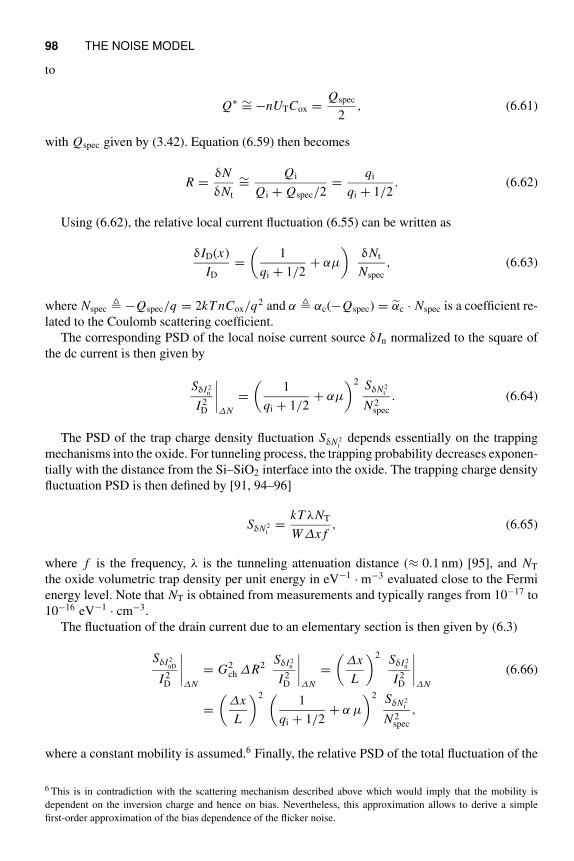
98 THE NOISE MODEL
to
Q∗ ∼= −nUTCox =Qspec
2, (6.61)
with Qspec given by (3.42). Equation (6.59) then becomes
R =δN
δNt
∼=Qi
Qi + Qspec/2=
qi
qi + 1/2. (6.62)
Using (6.62), the relative local current fluctuation (6.55) can be written as
δID(x)
ID
=(
1
qi + 1/2+ αµ
)δNt
Nspec
, (6.63)
where Nspec −Qspec/q = 2kT nCox/q2 and α αc(−Qspec) = αc · Nspec is a coefficient re-
lated to the Coulomb scattering coefficient.
The corresponding PSD of the local noise current source δIn normalized to the square of
the dc current is then given by
SδI 2n
I 2D
∣∣∣∣∆N
=(
1
qi + 1/2+ αµ
)2 SδN 2t
N 2spec
. (6.64)
The PSD of the trap charge density fluctuation SδN 2t
depends essentially on the trapping
mechanisms into the oxide. For tunneling process, the trapping probability decreases exponen-
tially with the distance from the Si–SiO2 interface into the oxide. The trapping charge density
fluctuation PSD is then defined by [91, 94–96]
SδN 2t
=kT λNT
W∆x f, (6.65)
where f is the frequency, λ is the tunneling attenuation distance (≈ 0.1 nm) [95], and NT
the oxide volumetric trap density per unit energy in eV−1 · m−3 evaluated close to the Fermi
energy level. Note that NT is obtained from measurements and typically ranges from 10−17 to
10−16 eV−1 · cm−3.
The fluctuation of the drain current due to an elementary section is then given by (6.3)
SδI 2nD
I 2D
∣∣∣∣∆N
= G2ch ∆R2
SδI 2n
I 2D
∣∣∣∣∆N
=(
∆x
L
)2 SδI 2n
I 2D
∣∣∣∣∆N
(6.66)
=(
∆x
L
)2 (1
qi + 1/2+ α µ
)2 SδN 2t
N 2spec
,
where a constant mobility is assumed.6 Finally, the relative PSD of the total fluctuation of the
6 This is in contradiction with the scattering mechanism described above which would imply that the mobility is
dependent on the inversion charge and hence on bias. Nevertheless, this approximation allows to derive a simple
first-order approximation of the bias dependence of the flicker noise.
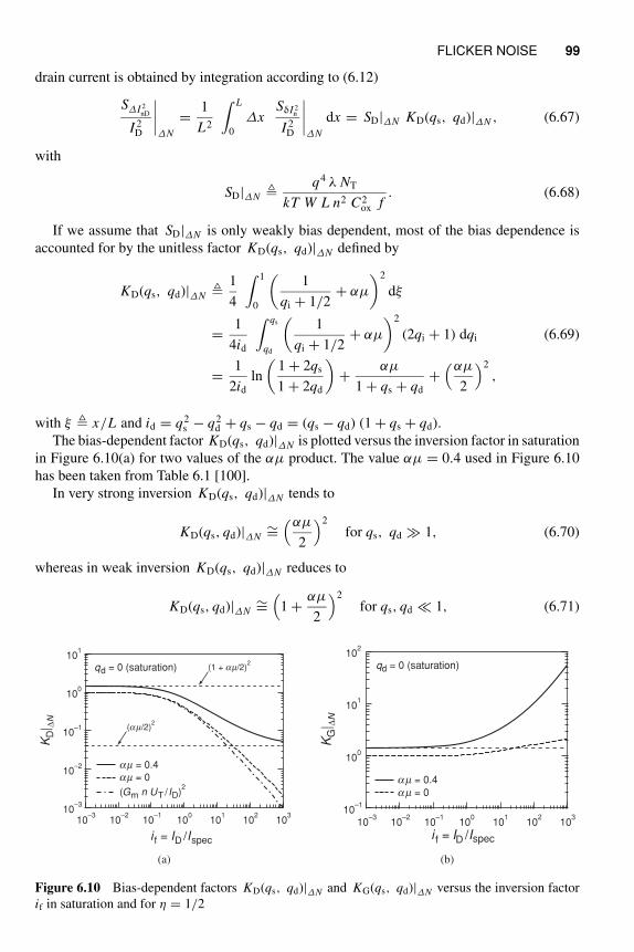
FLICKER NOISE 99
drain current is obtained by integration according to (6.12)
S∆I 2nD
I 2D
∣∣∣∣∆N
=1
L2
∫ L
0
∆xSδI 2
n
I 2D
∣∣∣∣∆N
dx = SD|∆N KD(qs, qd)|∆N , (6.67)
with
SD|∆N q4 λ NT
kT W L n2 C2ox f
. (6.68)
If we assume that SD|∆N is only weakly bias dependent, most of the bias dependence is
accounted for by the unitless factor KD(qs, qd)|∆N defined by
KD(qs, qd)|∆N 1
4
∫ 1
0
(1
qi + 1/2+ αµ
)2
dξ
=1
4id
∫ qs
qd
(1
qi + 1/2+ αµ
)2
(2qi + 1) dqi (6.69)
=1
2id
ln
(1 + 2qs
1 + 2qd
)+
αµ
1 + qs + qd
+(αµ
2
)2
,
with ξ x/L and id = q2s − q2
d + qs − qd = (qs − qd) (1 + qs + qd).
The bias-dependent factor KD(qs, qd)|∆N is plotted versus the inversion factor in saturation
in Figure 6.10(a) for two values of the αµ product. The value αµ = 0.4 used in Figure 6.10
has been taken from Table 6.1 [100].
In very strong inversion KD(qs, qd)|∆N tends to
KD(qs, qd)|∆N∼=
(αµ
2
)2
for qs, qd ≫ 1, (6.70)
whereas in weak inversion KD(qs, qd)|∆N reduces to
KD(qs, qd)|∆N∼=
(1 +
αµ
2
)2
for qs, qd ≪ 1, (6.71)
10–3
10–2
10–1
100
101
KD
| ∆N
10–3
10–2
10–1
100
101
102
103
i f = ID /Ispec
qd = 0 (saturation)
am = 0.4
am = 0
(Gm n UT / ID)2
(1 + am/2)2
(am/2)2
(a)
10–1
100
101
102
KG
| ∆N
10–3
10–2
10–1
100
101
102
103
i f = ID /Ispec
a m = 0.4
a m = 0
qd = 0 (saturation)
(b)
Figure 6.10 Bias-dependent factors KD(qs, qd)|∆N and KG(qs, qd)|∆N versus the inversion factor
if in saturation and for η = 1/2
100 THE NOISE MODEL
which is equal to unity when the mobility fluctuations induced by the carrier trapping mecha-
nism can be ignored (i.e., for α = 0).
As shown in Figure 6.10(a), the behavior of KD(qs, qd)|∆N very much depends on the value
of the αµ product. For values of αµ that get close to unity, KD(qs, qd)|∆N starts to saturate
to (αµ/2)2 in very strong inversion. On the other hand, for small values of αµ, Figure 6.10(a)
shows that KD(qs, qd)|∆N is very close to the square of normalized Gm/ID curve.
For circuit design, it is more useful to refer the flicker noise PSD at the gate by dividing
S∆I 2nD
∣∣∣∆N
by G2m, resulting in
S∆V 2G
∣∣∣∆N
S∆I 2nD
∣∣∣∆N
G2m
= SD|∆N KD(qs, qd)|∆N
(ID
Gm
)2
(6.72)
= SG|∆N KG(qs, qd)|∆N ,
where
SG|∆N q2 kT λ NT
W L C2ox f
. (6.73)
Assuming again that SG|∆N is only weakly bias dependent, most of the bias dependence is
captured by the factor KG(qs, qd)|∆N defined by
KG(qs, qd)|∆N (1 + qs + qd)2 KD(qs, qd)|∆N . (6.74)
The bias-dependent term KG(qs, qd)|∆N is plotted versus the inversion factor in saturation
in Figure 6.10(b) for the same values of αµ used in Figure 6.10(a). As explained above,
when the correlation term αµ is much smaller than 1, KD(qs, qd)|∆N is approximately equal
to (GmnUT/ID)2 in saturation and hence KG(qs, qd)|∆N is only weakly bias dependent. As
shown in Figure 6.10(b), for α = 0, it approximately changes only by a factor 2 over 6 decades
of current. This is no more the case when αµ gets closer to 1. In this case the gate-referred
flicker noise starts to increase significantly in strong inversion. Figure 6.10(b) also indicates
that the flicker noise referred to the gate in saturation and due to number fluctuation is minimum
in weak inversion.
The source of flicker noise coming from the fluctuation of the mobility will be discussed in
the next section.
6.3.2 Mobility Fluctuations (Hooge Model)
In the Hooge model [101], the drain current noise results from the fluctuations of the carrier
mobility. The PSD of the local noise current source of an elementary section is given by [91]
SδI 2n
I 2D
∣∣∣∣∆µ
=αH q
W ∆x (−Qi) f, (6.75)
where αH is the Hooge parameter which is unitless and ranges from about 10−4 to 10−6.
Assuming a constant average mobility, the fluctuation of the drain current due to an elementary
FLICKER NOISE 101
channel section is then given by (6.11)
SδI 2nD
I 2D
∣∣∣∣∆µ
=(
∆x
L
)2 SδI 2n
I 2D
∣∣∣∣∆µ
=∆x αH q
W L2 (−Qi) f. (6.76)
The PSD of the total fluctuation of the drain current is then given by
S∆I 2nD
I 2D
∣∣∣∣∆µ
= SD|∆µ KD(qs, qd)|∆µ , (6.77)
with
SD|∆µ αH q2
kT W L nCox f, (6.78)
and where KD(qs, qd)|∆µ accounts for the bias dependence and is defined by
KD(qs, qd)|∆µ
∫ 1
0
dξ
2qi(ξ )=
1
id
∫ qs
qd
(1 +
1
2qi
)dqi =
=1
id
[qs − qd +
1
2ln
(qs
qd
)](6.79)
=1
1 + qs + qd
[1 +
ln (qs/qd)
2(qs − qd)
].
The bias-dependent factor KD(qs, qd)|∆µ is plotted versus the inversion factor in satu-
ration (i.e., assuming a constant ratio qs/qd = 100) in Figure 6.11(a). In weak inversion,
KD(qs, qd)|∆µ is approximately given by
KD(qs, qd)|∆µ∼=
ln (qs/qd)
2(qs − qd)=
ln (if/ ir)
2id
=VDS/UT
2id
, (6.80)
10–2
10–1
100
101
102
103
104
10–3
10–2
10–1
100
101
102
103
i f = ID / Ispec
qs / qd = 100
(saturation)
KD
∆m
(a)
100
101
102
103
104
10–3
10–2
10–1
100
101
102
103
i f = ID / Ispec
qs / qd = 100
(saturation)
KG
∆m
(b)
Figure 6.11 Bias-dependent factors KD(qs, qd)|∆µ and KG(qs, qd)|∆µ versus the inversion factor if
in saturation (i.e., for qs/qd = 100)
102 THE NOISE MODEL
whereas in strong inversion, it is given by
KD(qs, qd)|∆µ∼=
1
qs + qd
=1
√if +
√ir
. (6.81)
The gate-referred noise PSD of the drain current fluctuations PSD is given by
S∆V 2G
∣∣∣∆µ
S∆I 2nD
∣∣∣∆µ
G2m
= SD|∆µ KD(qs, qd)|∆µ
(ID
Gm
)2
(6.82)
= SG|∆µ KG(qs, qd)|∆µ,
where
SG|∆µ kT n αH
W L Cox f, (6.83)
and
KG(qs, qd)|∆µ (1 + qs + qd)2 KD(qs, qd)|∆µ
= (1 + qs + qd)
[1 +
ln (qs/qd)
2(qs − qd)
]. (6.84)
Bias-dependent factor KG(qs, qd)|∆µ is plotted versus the inversion factor if in saturation
in Figure 6.11(b). It shows that for a given qs/qd ratio (or equivalently a given VDS voltage),
KG(qs, qd)|∆µ is decreasing like 1/ id in weak inversion
KG(qs, qd)|∆µ∼=
ln (qs/qd)
2(qs − qd)=
ln (if/ ir)
2id
=VDS/UT
2id
. (6.85)
In strong inversion, KG(qs, qd)|∆µ is approximately given by
KG(qs, qd)|∆µ∼= qs + qd =
√if +
√ir, (6.86)
and hence increases like√
if in very strong inversion and in saturation.
Unlike S∆V 2G
∣∣∣∆N
, which is minimum in weak inversion, Figure 6.11(b) shows that S∆V 2G
∣∣∣∆µ
is minimum in moderate inversion (in saturation as well as in the linear region).
6.3.3 Additional Contributions Due to the Source and DrainAccess Resistances
An additional contribution arises from the 1/ f noise generated in the source and drain access
resistances [102, 103]. The latter is modeled by two voltage sources in series with the source
and drain resistances RS and RD respectively. Assuming that RS = RD = Ra/2, the PSD of
FLICKER NOISE 103
the resulting drain current fluctuations is given by
S∆I 2nD
∣∣∣∆R
=G2
ms + G2md
[1 + (Gms + Gmd) Ra/2]2S∆V 2
R, (6.87)
where S∆V 2R
is the PSD of the 1/f noise voltage sources in series with the access resistances.
Assuming that (Gms + Gmd) Ra/2 ≪ 1, the PSD normalized to the square of the drain current
is then given by
S∆I 2nD
I 2D
∣∣∣∣∆R
∼= (G2ms + G2
md)S∆V 2
R
I 2D
. (6.88)
Now, the PSD of the voltage source S∆V 2R
is related to the PSD of the resistance fluctuation
S∆R2 by
S∆V 2R
= I 2D S∆R2 . (6.89)
Equation (6.88) then reduces to
S∆I 2nD
I 2D
∣∣∣∣∆R
= (G2ms + G2
md) S∆R2 = (q2s + q2
d ) G2spec S∆R2 . (6.90)
In strong inversion and in saturation, (6.90) becomes
S∆I 2nD
I 2D
∣∣∣∣∆R
= G2ms S∆R2 = q2
s G2spec S∆R2 = 2nβ ID S∆R2 . (6.91)
Assuming that S∆R2 is only weakly bias dependent, (6.91) shows that the contribution of the
access resistances to the flicker noise at the drain in strong inversion sharply increases with
the drain current (actually proportionally to I 3D). Hence the access resistances will mostly
contribute at high current level and should be negligible in moderate and weak inversion.
6.3.4 Total 1/f Noise at the Drain
The total 1/ f noise at the drain is given by the sum of the different contributions described
above [95, 100]
S∆I 2nD
I 2D
=S∆I 2
nD
I 2D
∣∣∣∣∆N
+S∆I 2
nD
I 2D
∣∣∣∣∆µ
+S∆I 2
nD
I 2D
∣∣∣∣∆R
. (6.92)
S∆I 2nD
/I 2D and the different contributions have been computed using the parameters given in
Table 6.1 which have been taken from reference [100]. The results obtained for VDS = 50 mV7
are plotted versus the inversion factor in Figure 6.12. It can be seen that the contribution coming
7 The VDS = 50 mV bias voltage is not very representative for analog circuit design since most of the time the
transistors are biased in saturation, except for switches which have a zero VDS. It has been chosen mainly to be able
to compare the results to the experimental measurements presented in [100], which are the only recent measurements
found where the PSD is plotted versus the current over a wide bias range.
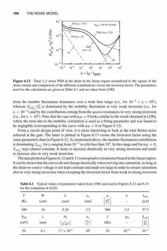
104 THE NOISE MODEL
10–10
10–9
10–8
10–7
S∆
I2 nD /
I D2 (
1/H
z)
10–3
10–2
10–1
100
101
102
103
i f = ID / Ispec
∆N (am = 0.4)
Total (am = 0.4)
∆m
∆R
VDS = 50 mV (linear)
Total
(am = 0)
∆N (am = 0)
Figure 6.12 Total 1/ f noise PSD at the drain in the linear region normalized to the square of the
drain current and comparison of the different contributions versus the inversion factor. The parameters
used for the calculation are given in Table 6.1 and are taken from [100]
from the number fluctuation dominates over a wide bias range (i.e., for 10−2 < if < 102),
whereas S∆I 2nD
/I 2D is dominated by the mobility fluctuation at very weak inversion (i.e., for
if < 10−2) and by the contribution coming from the access resistances in very strong inversion
(i.e., for if > 102). Note that the case with αµ = 0 looks similar to the result obtained in [100],
where the term due to the mobility correlation is used as a fitting parameter and was found to
be negligible (corresponding to the curve with αµ = 0 in Figure 6.12).
From a circuit design point of view, it is more interesting to look at the total flicker noise
referred at the gate. The latter is plotted in Figure 6.13 versus the inversion factor using the
same parameters than in Figure 6.12. As mentioned above, the number fluctuation contribution
is dominating S∆V 2G
for if ranging from 10−2 to a bit less than 102. In this range and for αµ = 0,
S∆V 2G
stays almost constant. It starts to increase drastically in very strong inversion and tends
to increase also in very weak inversion.
The data plotted in Figures 6.12 and 6.13 correspond to a transistor biased in the linear region.
It can be shown that the curves do not change drastically when moving into saturation, as long as
the drain-to-source voltage is not kept constant and made too large in order to ensure saturation
also in very strong inversion when sweeping the inversion factor from weak to strong inversion
Table 6.1 Typical values of parameters taken from [100] and used in Figures 6.12 and 6.13
for the evaluation of (6.92)
T W L tox µ n Ispec
[K] [μm] [μm] [nm]
[cm2
V·s
]– [μA]
300 10 0.18 3.5 560 1.4 57.5
VDS λ NT αc f αH S∆R2
[mV] [nm][
1
eV·cm3
] [V·sC
][Hz] –
[Ω2
Hz
]
50 0.1 7.7 × 10¹⁷ 104 10 10−6 10−6
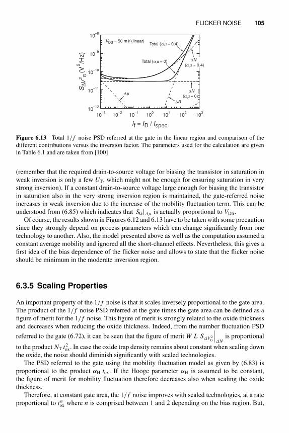
FLICKER NOISE 105
10–12
10–11
10–10
10–9
10–8
S∆V
2G (
V2/H
z)
10–3
10–2
10–1
100
101
102
103
if = ID / Ispec
∆N(a m = 0.4)
Total (am = 0.4)
∆m
∆R
VDS = 50 mV (linear)
Total (am = 0)
∆N(a m = 0)
Figure 6.13 Total 1/ f noise PSD referred at the gate in the linear region and comparison of the
different contributions versus the inversion factor. The parameters used for the calculation are given
in Table 6.1 and are taken from [100]
(remember that the required drain-to-source voltage for biasing the transistor in saturation in
weak inversion is only a few UT, which might not be enough for ensuring saturation in very
strong inversion). If a constant drain-to-source voltage large enough for biasing the transistor
in saturation also in the very strong inversion region is maintained, the gate-referred noise
increases in weak inversion due to the increase of the mobility fluctuation term. This can be
understood from (6.85) which indicates that SG|∆µ is actually proportional to VDS.
Of course, the results shown in Figures 6.12 and 6.13 have to be taken with some precaution
since they strongly depend on process parameters which can change significantly from one
technology to another. Also, the model presented above as well as the computation assumed a
constant average mobility and ignored all the short-channel effects. Nevertheless, this gives a
first idea of the bias dependence of the flicker noise and allows to state that the flicker noise
should be minimum in the moderate inversion region.
6.3.5 Scaling Properties
An important property of the 1/ f noise is that it scales inversely proportional to the gate area.
The product of the 1/ f noise PSD referred at the gate times the gate area can be defined as a
figure of merit for the 1/ f noise. This figure of merit is strongly related to the oxide thickness
and decreases when reducing the oxide thickness. Indeed, from the number fluctuation PSD
referred to the gate (6.72), it can be seen that the figure of merit W L S∆V 2G
∣∣∣∆N
is proportional
to the product NT t2ox. In case the oxide trap density remains about constant when scaling down
the oxide, the noise should diminish significantly with scaled technologies.
The PSD referred to the gate using the mobility fluctuation model as given by (6.83) is
proportional to the product αH tox. If the Hooge parameter αH is assumed to be constant,
the figure of merit for mobility fluctuation therefore decreases also when scaling the oxide
thickness.
Therefore, at constant gate area, the 1/ f noise improves with scaled technologies, at a rate
proportional to tnox where n is comprised between 1 and 2 depending on the bias region. But,
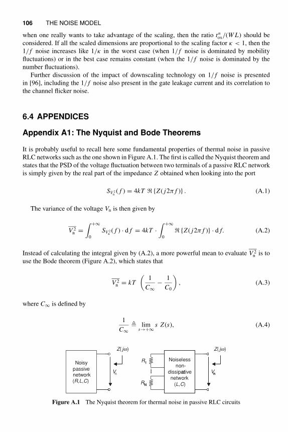
106 THE NOISE MODEL
when one really wants to take advantage of the scaling, then the ratio tnox/(W L) should be
considered. If all the scaled dimensions are proportional to the scaling factor κ < 1, then the
1/ f noise increases like 1/κ in the worst case (when 1/ f noise is dominated by mobility
fluctuations) or in the best case remains constant (when the 1/ f noise is dominated by the
number fluctuations).
Further discussion of the impact of downscaling technology on 1/ f noise is presented
in [96], including the 1/ f noise also present in the gate leakage current and its correlation to
the channel flicker noise.
6.4 APPENDICES
Appendix A1: The Nyquist and Bode Theorems
It is probably useful to recall here some fundamental properties of thermal noise in passive
RLC networks such as the one shown in Figure A.1. The first is called the Nyquist theorem and
states that the PSD of the voltage fluctuation between two terminals of a passive RLC network
is simply given by the real part of the impedance Z obtained when looking into the port
SV 2n( f ) = 4kT ℜ Z ( j2π f ) . (A.1)
The variance of the voltage Vn is then given by
V 2n =
∫ +∞
0
SV 2n( f ) · d f = 4kT ·
∫ +∞
0
ℜ Z ( j2π f ) · d f. (A.2)
Instead of calculating the integral given by (A.2), a more powerful mean to evaluate V 2n is to
use the Bode theorem (Figure A.2), which states that
V 2n = kT
(1
C∞−
1
C0
), (A.3)
where C∞ is defined by
1
C∞ lim
s→+∞s Z (s), (A.4)
Noisy
passivetwork
(R,L,C)
Vn
Z( jw) Z( jw)
Noiselessnon-
dissipativenetwork
(L,C)
Vn
R1
RN
at n
1
N
nne
Figure A.1 The Nyquist theorem for thermal noise in passive RLC circuits
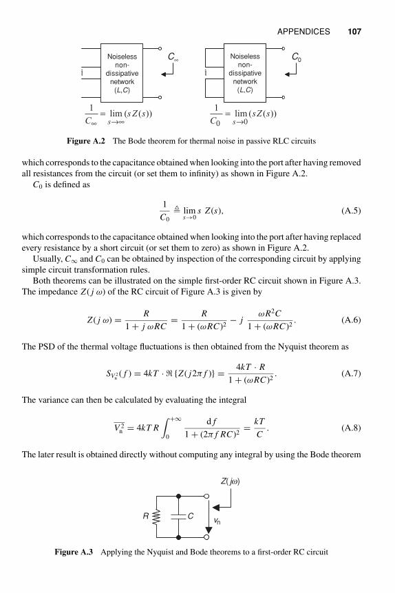
APPENDICES 107
Noiselessnon-
dissipativenetwork
(L,C)
))(( )(lim1
sZsC s
=∞→∞
C∞Noiseless
non-dissipative
network(L,C)
)(lim1
sZsC s
=0→0
C0
Figure A.2 The Bode theorem for thermal noise in passive RLC circuits
which corresponds to the capacitance obtained when looking into the port after having removed
all resistances from the circuit (or set them to infinity) as shown in Figure A.2.
C0 is defined as
1
C0
lims→0
s Z (s), (A.5)
which corresponds to the capacitance obtained when looking into the port after having replaced
every resistance by a short circuit (or set them to zero) as shown in Figure A.2.
Usually, C∞ and C0 can be obtained by inspection of the corresponding circuit by applying
simple circuit transformation rules.
Both theorems can be illustrated on the simple first-order RC circuit shown in Figure A.3.
The impedance Z ( j ω) of the RC circuit of Figure A.3 is given by
Z ( j ω) =R
1 + j ωRC=
R
1 + (ωRC)2− j
ωR2C
1 + (ωRC)2. (A.6)
The PSD of the thermal voltage fluctuations is then obtained from the Nyquist theorem as
SV 2n( f ) = 4kT · ℜ Z ( j2π f ) =
4kT · R
1 + (ωRC)2. (A.7)
The variance can then be calculated by evaluating the integral
V 2n = 4kT R
∫ +∞
0
d f
1 + (2π f RC)2=
kT
C. (A.8)
The later result is obtained directly without computing any integral by using the Bode theorem
R
Z( jw)
C vn
Figure A.3 Applying the Nyquist and Bode theorems to a first-order RC circuit
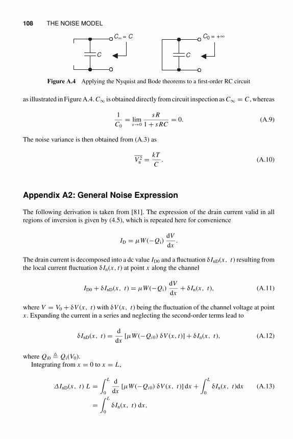
108 THE NOISE MODEL
C∞ = C
C
C0 = +∞
C
Figure A.4 Applying the Nyquist and Bode theorems to a first-order RC circuit
as illustrated in Figure A.4. C∞ is obtained directly from circuit inspection as C∞ = C , whereas
1
C0
= lims→0
s R
1 + s RC= 0. (A.9)
The noise variance is then obtained from (A.3) as
V 2n =
kT
C. (A.10)
Appendix A2: General Noise Expression
The following derivation is taken from [81]. The expression of the drain current valid in all
regions of inversion is given by (4.5), which is repeated here for convenience
ID = µW (−Qi)dV
dx.
The drain current is decomposed into a dc value ID0 and a fluctuation δInD(x, t) resulting from
the local current fluctuation δIn(x, t) at point x along the channel
ID0 + δInD(x, t) = µW (−Qi)dV
dx+ δIn(x, t), (A.11)
where V = V0 + δV (x, t) with δV (x, t) being the fluctuation of the channel voltage at point
x . Expanding the current in a series and neglecting the second-order terms lead to
δInD(x, t) =d
dx[µW (−Qi0) δV (x, t)] + δIn(x, t), (A.12)
where Qi0 Qi(V0).
Integrating from x = 0 to x = L ,
∆InD(x, t) L =∫ L
0
d
dx[µW (−Qi0) δV (x, t)] dx +
∫ L
0
δIn(x, t)dx (A.13)
=∫ L
0
δIn(x, t) dx,
APPENDICES 109
since in short-circuit condition, δV = 0 at x = 0 and x = L . The autocorrelation function of
∆InD is then given by
R∆I 2nD
(τ ) = δInD(t) δInD(t + τ ) (A.14)
=1
L2
∫ L
0
∫ L
0
δIn(x, t) δIn(x ′, t + τ ) dx dx ′.
The PSD of ∆InD is then given by
S∆I 2nD
(ω) =1
L2
∫ L
0
∫ L
0
SδInδI ′n(x, x ′, ω) dx dx ′, (A.15)
where SδInδI ′n(x, x ′, ω) is the cross-power spectral density (CPSD) between noise at points x
and x ′. If there is no spatial correlation, then SδInδI ′n(x, x ′, ω) is a Dirac impulse located at
point x ′ − x
SδInδI ′n(x, x ′, ω) = F(x, ω) δ(x ′ − x). (A.16)
Equation (A.15) then reduces to
S∆I 2nD
(ω) =1
L2
∫ L
0
F(x, ω) dx . (A.17)
Applying (A.17) to only one noisy section between x and x + ∆x leads to
SδI 2nD
(ω) =F(x, ω)
∆x, (A.18)
which relates F(x, ω) to the PSD of the noise of a single section SδI 2n(x, ω)
F(x, ω) = ∆x SδI 2n(x, ω). (A.19)
Finally, (A.17) can be written as
S∆I 2nD
(ω) =1
L2
∫ L
0
∆x SδI 2n(x, ω) dx . (A.20)

7 Temperature Effectsand Matching
This chapter models variations of the transistor characteristics, which are very important issues
in circuit design. Section 7.2 considers variations with the temperature, which constitute the
main external perturbation on transistor characteristics. Section 7.3 is dedicated to the problem
of mismatch between the characteristics of supposedly identical transistors, which is a very
important limitation to the performance of most analog circuits. These two kinds of variations
will be characterized as variations of the basic model parameters established so far, and will
be traced back to variations of physical parameters.
7.1 INTRODUCTION
The purpose of a transistor model is to describe its electrical characteristics. These are essen-
tially the static and dynamic relationships between the voltages applied at its various terminals
and the currents flowing through them.
The model introduced so far describes how these electrical characteristics depend on phys-
ical parameters. These physical parameters have been lumped into a reduced set of model
parameters. As long as the physical parameters remain constant, the characteristics and the
model parameters remain constant. However, some physical parameters may change, thereby
modifying the transistor characteristics.
Aging is the consequence of parameters changing with time. It will not be considered here.
Many parameters are changing with the temperature, which can be considered the main
external perturbation on the transistor.
The characteristics of two or more transistors designed to be identical do not match perfectly.
This mismatch is the consequence of parameters changing in space.
A list of all basic parameters that influence the characteristics of the transistor is given in
Table 7.1. It indicates which of them depend on the temperature and which of them may change
spatially, resulting in mismatch.
Charge-Based MOS Transistor Modeling: The EKV Model for Low-Power and RF IC Design C. Enz and E. VittozC© 2006 John Wiley & Sons, Ltd.
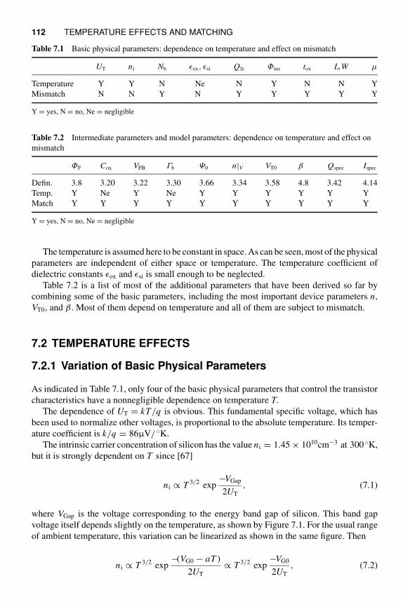
112 TEMPERATURE EFFECTS AND MATCHING
Table 7.1 Basic physical parameters: dependence on temperature and effect on mismatch
UT ni Nb ǫox, ǫsi Qfc Φms tox L,W μ
Temperature Y Y N Ne N Y N N Y
Mismatch N N Y N Y Y Y Y Y
Y = yes, N = no, Ne = negligible
Table 7.2 Intermediate parameters and model parameters: dependence on temperature and effect on
mismatch
ΦF Cox VFB Γb Ψ0 n|V VT0 β Qspec Ispec
Defin. 3.8 3.20 3.22 3.30 3.66 3.34 3.58 4.8 3.42 4.14
Temp. Y Ne Y Ne Y Y Y Y Y Y
Match Y Y Y Y Y Y Y Y Y Y
Y = yes, N = no, Ne = negligible
The temperature is assumed here to be constant in space. As can be seen, most of the physical
parameters are independent of either space or temperature. The temperature coefficient of
dielectric constants ǫox and ǫsi is small enough to be neglected.
Table 7.2 is a list of most of the additional parameters that have been derived so far by
combining some of the basic parameters, including the most important device parameters n,
VT0, and β. Most of them depend on temperature and all of them are subject to mismatch.
7.2 TEMPERATURE EFFECTS
7.2.1 Variation of Basic Physical Parameters
As indicated in Table 7.1, only four of the basic physical parameters that control the transistor
characteristics have a nonnegligible dependence on temperature T.
The dependence of UT = kT/q is obvious. This fundamental specific voltage, which has
been used to normalize other voltages, is proportional to the absolute temperature. Its temper-
ature coefficient is k/q = 86μV/ K.
The intrinsic carrier concentration of silicon has the value ni = 1.45 × 1010cm−3 at 300 K,
but it is strongly dependent on T since [67]
ni ∝ T 3/2 exp−VGap
2UT
, (7.1)
where VGap is the voltage corresponding to the energy band gap of silicon. This band gap
voltage itself depends slightly on the temperature, as shown by Figure 7.1. For the usual range
of ambient temperature, this variation can be linearized as shown in the same figure. Then
ni ∝ T 3/2 exp−(VG0 − aT )
2UT
∝ T 3/2 exp−VG0
2UT
, (7.2)
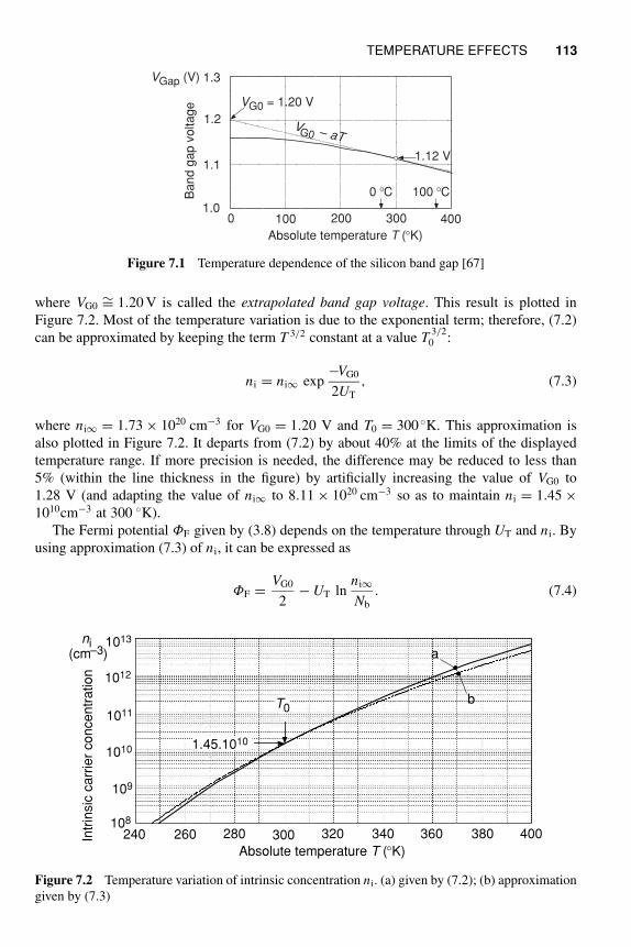
TEMPERATURE EFFECTS 113
VG0 = 1.20 V
0 °C 100 °C
VG0 – aT
1.12 V
0 100 200 300 4001.0
1.1
1.3
1.2
Ba
nd
ga
p v
olta
ge
VGap (V)
Absolute temperature T (°K)
Figure 7.1 Temperature dependence of the silicon band gap [67]
where VG0∼= 1.20 V is called the extrapolated band gap voltage. This result is plotted in
Figure 7.2. Most of the temperature variation is due to the exponential term; therefore, (7.2)
can be approximated by keeping the term T 3/2 constant at a value T3/2
0 :
ni = ni∞ exp−VG0
2UT
, (7.3)
where ni∞ = 1.73 × 1020 cm−3 for VG0 = 1.20 V and T0 = 300 K. This approximation is
also plotted in Figure 7.2. It departs from (7.2) by about 40% at the limits of the displayed
temperature range. If more precision is needed, the difference may be reduced to less than
5% (within the line thickness in the figure) by artificially increasing the value of VG0 to
1.28 V (and adapting the value of ni∞ to 8.11 × 1020 cm−3 so as to maintain ni = 1.45 ×1010cm−3 at 300 K).
The Fermi potential ΦF given by (3.8) depends on the temperature through UT and ni. By
using approximation (7.3) of ni, it can be expressed as
ΦF =VG0
2− UT ln
ni∞
Nb
. (7.4)
1013
240 400260 280 300 320 340 360 380
1012
1011
1010
108
109
T0
1.45.1010
a
b
Absolute temperature T (°K)
ni(cm–3)
Intr
insic
ca
rrie
r co
nce
ntr
atio
n
Figure 7.2 Temperature variation of intrinsic concentration ni. (a) given by (7.2); (b) approximation
given by (7.3)
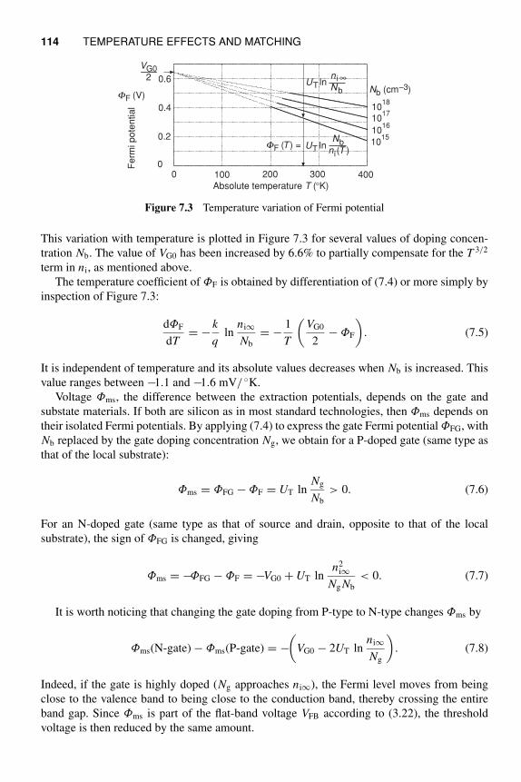
114 TEMPERATURE EFFECTS AND MATCHING
0
0.2
0.4
0.6
0 100 200 300 400
Absolute temperature T (°K)
Nb (cm–3)
1015
1018
1017
1016
Ferm
i pote
ntial
FF (V)
VG02 n i ∞
NbUT ln
UT lnNb
ni(T )FF (T ) =
Figure 7.3 Temperature variation of Fermi potential
This variation with temperature is plotted in Figure 7.3 for several values of doping concen-
tration Nb. The value of VG0 has been increased by 6.6% to partially compensate for the T 3/2
term in ni, as mentioned above.
The temperature coefficient of ΦF is obtained by differentiation of (7.4) or more simply by
inspection of Figure 7.3:
dΦF
dT= −
k
qln
ni∞
Nb
= −1
T
(VG0
2− ΦF
)
. (7.5)
It is independent of temperature and its absolute values decreases when Nb is increased. This
value ranges between −1.1 and −1.6 mV/ K.
Voltage Φms, the difference between the extraction potentials, depends on the gate and
substate materials. If both are silicon as in most standard technologies, then Φms depends on
their isolated Fermi potentials. By applying (7.4) to express the gate Fermi potential ΦFG, with
Nb replaced by the gate doping concentration Ng, we obtain for a P-doped gate (same type as
that of the local substrate):
Φms = ΦFG − ΦF = UT lnNg
Nb
> 0. (7.6)
For an N-doped gate (same type as that of source and drain, opposite to that of the local
substrate), the sign of ΦFG is changed, giving
Φms = −ΦFG − ΦF = −VG0 + UT lnn2
i∞Ng Nb
< 0. (7.7)
It is worth noticing that changing the gate doping from P-type to N-type changes Φms by
Φms(N-gate) − Φms(P-gate) = −(
VG0 − 2UT lnni∞
Ng
)
. (7.8)
Indeed, if the gate is highly doped (Ng approaches ni∞), the Fermi level moves from being
close to the valence band to being close to the conduction band, thereby crossing the entire
band gap. Since Φms is part of the flat-band voltage VFB according to (3.22), the threshold
voltage is then reduced by the same amount.
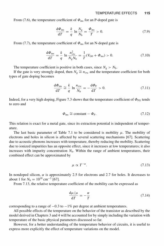
TEMPERATURE EFFECTS 115
From (7.6), the temperature coefficient of Φms for an P-doped gate is
dΦms
dT=
k
qln
Ng
Nb
=Φms
T> 0. (7.9)
From (7.7), the temperature coefficient of Φms for an N-doped gate is
dΦms
dT=
k
qln
n2i∞
Ng Nb
=1
T(VG0 + Φms) > 0. (7.10)
The temperature coefficient is positive in both cases, since Ng > Nb.
If the gate is very strongly doped, then Ng∼= ni∞ and the temperature coefficient for both
types of gate doping becomes
dΦms
dT∼=
k
qln
ni∞
Nb
= −dΦF
dT> 0. (7.11)
Indeed, for a very high doping, Figure 7.3 shows that the temperature coefficient of ΦFG tends
to zero and
Φms∼= constant − ΦF. (7.12)
This relation is exact for a metal gate, since its extraction potential is independent of temper-
ature.
The last basic parameter of Table 7.1 to be considered is mobility μ. The mobility of
electrons and holes in silicon is affected by several scattering mechanisms [67]. Scattering
due to acoustic phonons increases with temperature, thereby reducing the mobility. Scattering
due to ionized impurities has an opposite effect, since it increases at low temperatures; it also
increases with impurity concentration Nb. Within the range of ambient temperatures, their
combined effect can be approximated by
μ ∝ T −α. (7.13)
In nondoped silicon, α is approximately 2.5 for electrons and 2.7 for holes. It decreases to
about 1 for Nb = 1018 cm−3 [67].
From 7.13, the relative temperature coefficient of the mobility can be expressed as
dμ/μ
dT= −
α
T(7.14)
corresponding to a range of −0.3 to −1% per degree at ambient temperatures.
All possible effects of the temperature on the behavior of the transistor as described by the
model derived in Chapters 3 and 4 will be accounted for by simply including the variation with
temperature of the basic physical parameters discussed so far.
However, for a better understanding of the temperature behavior of circuits, it is useful to
express more explicitly the effect of temperature variations on the model.
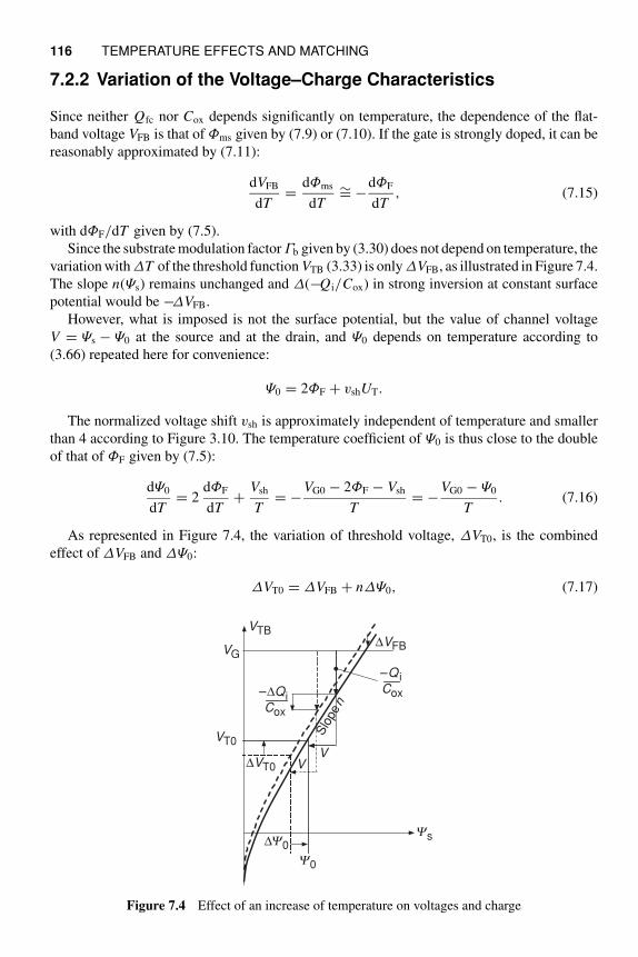
116 TEMPERATURE EFFECTS AND MATCHING
7.2.2 Variation of the Voltage–Charge Characteristics
Since neither Qfc nor Cox depends significantly on temperature, the dependence of the flat-
band voltage VFB is that of Φms given by (7.9) or (7.10). If the gate is strongly doped, it can be
reasonably approximated by (7.11):
dVFB
dT=
dΦms
dT∼= −
dΦF
dT, (7.15)
with dΦF/dT given by (7.5).
Since the substrate modulation factor Γb given by (3.30) does not depend on temperature, the
variation with ΔT of the threshold function VTB (3.33) is only ΔVFB, as illustrated in Figure 7.4.
The slope n(Ψs) remains unchanged and Δ(−Qi/Cox) in strong inversion at constant surface
potential would be −ΔVFB.
However, what is imposed is not the surface potential, but the value of channel voltage
V = Ψs − Ψ0 at the source and at the drain, and Ψ0 depends on temperature according to
(3.66) repeated here for convenience:
Ψ0 = 2ΦF + vshUT.
The normalized voltage shift vsh is approximately independent of temperature and smaller
than 4 according to Figure 3.10. The temperature coefficient of Ψ0 is thus close to the double
of that of ΦF given by (7.5):
dΨ0
dT= 2
dΦF
dT+
Vsh
T= −
VG0 − 2ΦF − Vsh
T= −
VG0 − Ψ0
T. (7.16)
As represented in Figure 7.4, the variation of threshold voltage, ΔVT0, is the combined
effect of ΔVFB and ΔΨ0:
ΔVT0 = ΔVFB + nΔΨ0, (7.17)
Y0
∆Y0Ys
VT0
∆VT0
∆VFB
Slo
pe n
VG
VTB
VV
–∆QiCox
–Q iCox
Figure 7.4 Effect of an increase of temperature on voltages and charge
TEMPERATURE EFFECTS 117
where slope n should be evaluated at V = 0: n = n0 given by (3.73). Hence
dVT0
dT=
dVFB
dT+ n0
dΨ0
dT(7.18)
as can be obtained directly by differentiation of expression (3.58) of the threshold VT0.
Now, for a highly doped gate, introducing approximation (7.15) with (7.16) and (7.5) yields
an explicit expression for the temperature coefficient of VT0:
dVT0
dT= (2n0 − 1)
dΦF
dT+ n0
Vsh
T=
(n0 − 1/2)(2ΦF − VG0) + n0Vsh
T, (7.19)
which is always negative. Using the first expression of dΦF/dT in (7.5), this temperature
coefficient can also be written as
dVT0
dT=
k
q
[
(1 − 2n0) lnni∞
Nb
+ n0vsh
]
, (7.20)
showing that, except for the slight variation of n0 to be discussed further, the temperature
coefficient of VT0 is independent of the temperature. Practical values are ranging from −2.5
to −1 mV/ K.
Although the slope factor n at constant Ψs is independent of temperature, at constant V =Ψs − Ψ0 it varies through the variation of Ψ0. By using (3.34), and (7.16),
dn
dT=
d
dΨ0
(
1 +Γb
2√
Ψ0 + V
)dΨ0
dT=
n − 1
2T
VG0 − Ψ0
V + Ψ0
, (7.21)
which is always positive. Practical values are never larger than 0.1%/ K; therefore, this vari-
ation can be neglected in most situations.
Neglecting the variation of n, the specific charge density Qspec defined by (3.42) and used
to normalize the density of inverted charge is simply proportional to UT; hence,
dQspec/Qspec
dT=
1
T. (7.22)
Since n can be considered constant, the variation of the pinch-off voltage at constant gate
voltage obtained from expression (3.63) becomes
dVP
dT= −
1
n
dVT0
dT. (7.23)
The temperature coefficient of −Qi for fixed voltages depends on the mode of operation.
For strong inversion, differentiating approximation (3.64) and introducing (7.23) yield
d(−Qi/Cox)
dT= −
dVT0
dT. (7.24)
This relation is also illustrated in Figure 7.4.
118 TEMPERATURE EFFECTS AND MATCHING
The behavior is more complicated in weak inversion. Approximation (3.49) can be rewritten:
−Qi = 2nCoxUT expVP − V
UT
, (7.25)
where UT and VP depend on temperature. Differentiation gives
dQi/Qi
dT=
V + UT − VP
T UT
−1
nUT
dVT 0
dT. (7.26)
Since in weak inversion V − VP is usually much smaller than VG0 − 2ΦF, an inspection of
expression (7.19) shows that the last term dominates. As for strong inversion above, the charge
increases with temperature. But the relative increase is maximum in weak inversion.
In summary, among the three device parameters controlling the charge–voltage character-
istics of the transistor, only VT0 is significantly dependent on the temperature. The variation of
Cox is negligible and that of n can usually be neglected.
7.2.3 Variation of the Voltage–Current Characteristics
The only additional parameter needed to obtain the current from the mobile charge density is
the transfer parameter β defined by (4.8). It is proportional to the mobility; hence, from (7.14),
dβ/β
dT= −
α
T. (7.27)
As seen previously, β can be replaced as the third parameter controlling the current by the
specific current Ispec that is used to normalize all currents. Differentiation of its expression
(4.14) gives
dIspec/Ispec
dT=
2 − α
T. (7.28)
We have seen that α > 2 for nondoped or lightly doped silicon, resulting in a negative tem-
perature coefficient of Ispec. For a doping concentration Nb = 1016 cm−3, α ∼= 2, the variation
of U 2T compensates that of β, and Ispec is approximately independent of the temperature. This
compensation disappears and the coefficient becomes positive when α is decreased below 2
by further increasing Nb.
The variation of current with temperature for constant bias voltages depends on the mode
of operation.
For strong inversion, the differentiation of approximation (4.28) gives
dIF,R/IF,R
dT=
dβ/β
dT−
2
n(VP − VS,D)
dVT0
dT. (7.29)
Since the temperature coefficients of VT0 and β are both negative, compensation occurs for a
particular value of n(VP − VS,D) = VG − VT0 − nVS,D. This value is ranging between 300 and
600 mV. Above this limit value, the variation of mobility dominates and the current decreases
TEMPERATURE EFFECTS 119
with increasing temperature. Below this limit, the variation of threshold dominates and the
current increases with the temperature.
For weak inversion, the differentiation of approximation (4.34) gives, after introduction of
(7.28)
dIF,R/IF,R
dT=
VS,D − VP + (2 − α)UT
T UT
−1
nUT
VT0
dT, (7.30)
which is very close to expression (7.26) for the charge. Here again the last term due to the
variation of threshold dominates. The current for constant bias voltages increases with tem-
perature.
This dependence is very large, typically 5% per degree, due to the strong effect of threshold
variations on the drain current (large transconductance to current ratio). For this reason, a
transistor in weak inversion should always be biased at constant current, and never at constant
gate and source voltages.
The specific conductance used to normalize transconductances is given by (5.6). Neglecting
again the variation of n, we obtain by differentiation
dGspec/Gspec
dT=
1 − α
T< 0. (7.31)
Since α > 1, this coefficient is always negative.
The transconductance for a given value of β may be imposed by the voltages or by the
current.
For strong inversion and constant voltages, the differentiation of (5.14) yields
dGms,d/Gms,d
dT=
dβ/β
dT−
1
n(VP − VS,D)
dVT0
dT. (7.32)
By comparing with (7.29), we can see that the sensitivity to threshold variations is half of that
for the current. The compensation of the variation of β therefore occurs for half the value of
n(VP − VS,D), in the range 150–300 mV.
For strong inversion and constant current, the differentiation of (5.16) yields
dGms,d/Gms,d
dT=
1
2
dβ/β
dT= −
α
2T. (7.33)
The relative temperature coefficient of the transconductance is always negative and independent
of the current.
As mentioned above, a transistor in weak inversion should always be biased at constant
current, the differentiation of (5.19) yields
dGms,d/Gms,d
dT= −
1
T. (7.34)
Results (7.33) and (7.34) are comparable. The temperature coefficient of the transconduc-
tance at constant current is always negative. It is about −0.3%/ K at ambient temperature.
120 TEMPERATURE EFFECTS AND MATCHING
7.2.4 Variation of the Current–Charge Characteristics
Relationship (4.19) between the normalized current and charge can be rewritten with nonnor-
malized variables:
β
2n
(−QiS,D
Cox
)2
+ βUT
−QiS,D
Cox
= IF,R, (7.35)
where the first term may be neglected in weak inversion and the second term may be neglected
in strong inversion. Differentiating separately these two components of the inverted charge
gives for strong inversion
dQiS,D/QiS,D
dT= −
1
2
dβ/β
dT=
α
2T. (7.36)
and for weak inversion
dQiS,D/QiS,D
dT= −
dβ/β
dT−
1
T=
α − 1
T. (7.37)
These results are comparable. The temperature coefficient of the charge at constant current is
always positive. It is about +0.3%/K at ambient temperature.
7.3 MATCHING
7.3.1 Introduction
Matching of the characteristics of two or several transistors is a very important consideration
for analog circuits. Even if transistors are exactly identical in their structure and layout, their
electrical behaviors are not exactly identical. This is due to spacial fluctuations of the physical
parameters that control these behaviors, as listed in Table 7.1.
As summarized in Section 4.4.2, the static voltage–current characteristics of long-channel
transistors require only three device parameters, namely VT0, β, and n. Hence, the mismatch
of their characteristics is completely characterized by the mismatch of these three parameters.
The sensitivity of these parameters to temperature has been discussed in Section 7.2. If
there is any difference in the temperature of two or several transistors, due to a gradient of
temperature on the chip, it produces a proportional difference in the parameters. This gradient
may be stationary (due to a source of heat on the chip), or it can be transient in time (due to a
change of ambient temperature that is too fast with respect to the chip thermal time constant).
Now, even if the temperature does not vary throughout the chip, some variations of the three
device parameters remain, which can be traced back to those of the physical parameters, as
illustrated in Figure 7.5.
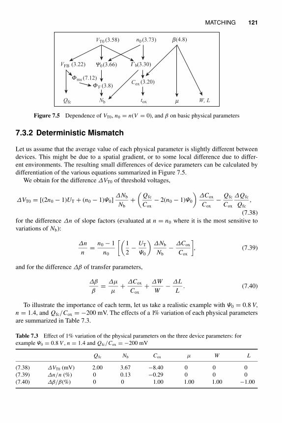
MATCHING 121
(3.58) (3.73) (4.8)
(3.30)
(3.20)
(3.66)(3.22)
(7.12)
(3.8)
W, Ltox
n0
NbQfc
VFB
VT0
Cox
m
b
GY
F
FF
ms
b0
Figure 7.5 Dependence of VT0, n0 = n(V = 0), and β on basic physical parameters
7.3.2 Deterministic Mismatch
Let us assume that the average value of each physical parameter is slightly different between
devices. This might be due to a spatial gradient, or to some local difference due to differ-
ent environments. The resulting small differences of device parameters can be calculated by
differentiation of the various equations summarized in Figure 7.5.
We obtain for the difference ΔVT0 of threshold voltages,
ΔVT0 = [(2n0 − 1)UT + (n0 − 1)Ψ0]ΔNb
Nb
+(
Qfc
Cox
− 2(n0 − 1)Ψ0
)ΔCox
Cox
−Qfc
Cox
ΔQfc
Qfc
,
(7.38)
for the difference Δn of slope factors (evaluated at n = n0 where it is the most sensitive to
variations of Nb):
Δn
n=
n0 − 1
n0
[(1
2−
UT
Ψ0
)ΔNb
Nb
−ΔCox
Cox
]
, (7.39)
and for the difference Δβ of transfer parameters,
Δβ
β=
Δμ
μ+
ΔCox
Cox
+ΔW
W−
ΔL
L. (7.40)
To illustrate the importance of each term, let us take a realistic example with Ψ0 = 0.8 V,
n = 1.4, and Qfc/Cox = −200 mV. The effects of a 1% variation of each physical parameters
are summarized in Table 7.3.
Table 7.3 Effect of 1% variation of the physical parameters on the three device parameters: for
example Ψ0 = 0.8 V , n = 1.4 and Qfc/Cox = −200 mV
Qfc Nb Cox μ W L
(7.38) ΔVT0 (mV) 2.00 3.67 −8.40 0 0 0
(7.39) Δn/n (%) 0 0.13 −0.29 0 0 0
(7.40) Δβ/β(%) 0 0 1.00 1.00 1.00 −1.00
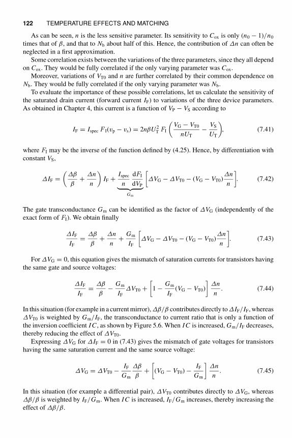
122 TEMPERATURE EFFECTS AND MATCHING
As can be seen, n is the less sensitive parameter. Its sensitivity to Cox is only (n0 − 1)/n0
times that of β, and that to Nb about half of this. Hence, the contribution of Δn can often be
neglected in a first approximation.
Some correlation exists between the variations of the three parameters, since they all depend
on Cox. They would be fully correlated if the only varying parameter was Cox.
Moreover, variations of VT0 and n are further correlated by their common dependence on
Nb. They would be fully correlated if the only varying parameter was Nb.
To evaluate the importance of these possible correlations, let us calculate the sensitivity of
the saturated drain current (forward current IF) to variations of the three device parameters.
As obtained in Chapter 4, this current is a function of VP − VS according to
IF = Ispec F I(vp − vs) = 2nβU 2T FI
(VG − VT0
nUT
−VS
UT
)
, (7.41)
where FI may be the inverse of the function defined by (4.25). Hence, by differentiation with
constant VS,
ΔIF =(
Δβ
β+
Δn
n
)
IF +Ispec
n
dFI
dVP︸ ︷︷ ︸
Gm
[
ΔVG − ΔVT0 − (VG − VT0)Δn
n
]
. (7.42)
The gate transconductance Gm can be identified as the factor of ΔVG (independently of the
exact form of FI). We obtain finally
ΔIF
IF
=Δβ
β+
Δn
n+
Gm
IF
[
ΔVG − ΔVT0 − (VG − VT0)Δn
n
]
. (7.43)
For ΔVG = 0, this equation gives the mismatch of saturation currents for transistors having
the same gate and source voltages:
ΔIF
IF
=Δβ
β−
Gm
IF
ΔVT0 +[
1 −Gm
IF
(VG − VT0)
]Δn
n. (7.44)
In this situation (for example in a current mirror), Δβ/β contributes directly to ΔIF/IF, whereas
ΔVT0 is weighted by Gm/IF, the transconductance to current ratio that is only a function of
the inversion coefficient I C , as shown by Figure 5.6. When I C is increased, Gm/IF decreases,
thereby reducing the effect of ΔVT0.
Expressing ΔVG for ΔIF = 0 in (7.43) gives the mismatch of gate voltages for transistors
having the same saturation current and the same source voltage:
ΔVG = ΔVT0 −IF
Gm
Δβ
β+
[
(VG − VT0) −IF
Gm
]Δn
n. (7.45)
In this situation (for example a differential pair), ΔVT0 contributes directly to ΔVG, whereas
Δβ/β is weighted by IF/Gm. When I C is increased, IF/Gm increases, thereby increasing the
effect of Δβ/β.
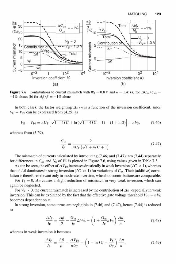
MATCHING 123
1 10210–2
Inversion coefficient IC104
(a)
0
5
10
15
20
25
30
–5
∆IFIF(%)
Cu
rre
nt
mis
ma
tch
Contribution of
∆n
∆n
∆b
∆VT0Total
VS = 0
VS = 1.0 V
∆CoxCox
= +1%(%)
Cu
rre
nt
mis
ma
tch
∆IFIF
0
–5
5
10
Contribution of
∆VT0
∆n
∆n
Total
Total VS = 0
VS = 1.0 V
(b)
1 10210–2
Inversion coefficient IC104
∆NbNb
= –1%
Figure 7.6 Contributions to current mismatch with Ψ0 = 0.8 V and n = 1.4: (a) for ΔCox/Cox =+1% alone; (b) for Δβ/β = −1% alone
In both cases, the factor weighting Δn/n is a function of the inversion coefficient, since
VG − VT0 can be expressed from (4.25) as
VG − VT0 = nUT
[√1 + 4I C + ln (
√1 + 4I C − 1) − (1 + ln 2)
]
+ nVS, (7.46)
whereas from (5.29),
Gm
IF
=2
nUT
(√1 + 4I C + 1
) . (7.47)
The mismatch of currents calculated by introducing (7.46) and (7.47) into (7.44) separately
for differences in Cox and Nb of 1% is plotted in Figure 7.6, using values given in Table 7.3.
As can be seen, the effect of ΔVT0 increases drastically in weak inversion (I C < 1), whereas
that of Δβ dominates in strong inversion (I C ≫ 1) for variations of Cox. Their (additive) corre-
lation is therefore relevant only in moderate inversion, when both contributions are comparable.
For VS = 0, Δn causes a slight reduction of mismatch in very weak inversion, which can
again be neglected.
For VS > 0, the current mismatch is increased by the contribution of Δn, especially in weak
inversion. This can be explained by the fact that the effective gate voltage threshold VT0 + nVS
becomes dependent on n.
In strong inversion, some terms are negligible in (7.46) and (7.47), hence (7.44) is reduced
to
ΔIF
IF
=Δβ
β−
Gm
IF
ΔVT0 −(
1 +Gm
IF
nVS
)Δn
n, (7.48)
whereas in weak inversion it becomes
ΔIF
IF
=Δβ
β−
ΔVT0
nUT
+(
1 − ln I C −VS
UT
)Δn
n. (7.49)
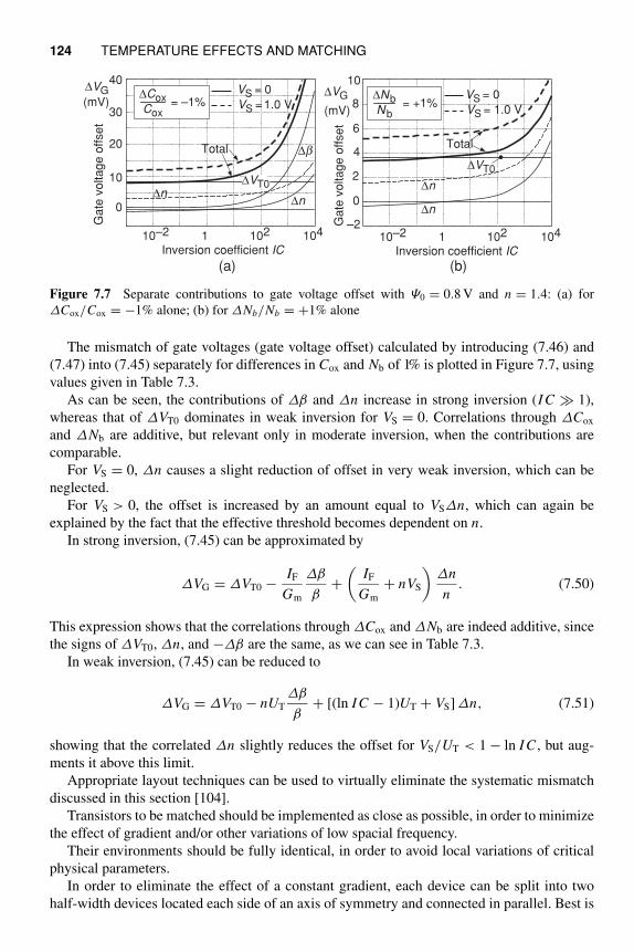
124 TEMPERATURE EFFECTS AND MATCHING
10
0
–2
2
4
6
8
1 10210–2
Inversion coefficient IC104
(b)
VS = 0
VS = 1.0 V
∆VT0
∆n
∆n
Total
∆NbNb
= +1%
Ga
te v
olta
ge
off
se
t
(mV)
40
30
20
10
0
1 10210–2
Inversion coefficient IC104
(a)
∆n∆n
∆bTotal
VS = 0
VS = 1.0 V∆CoxCox
= –1%G
ate
vo
lta
ge
off
se
t(mV)
∆VT0
∆VG ∆VG
Figure 7.7 Separate contributions to gate voltage offset with Ψ0 = 0.8 V and n = 1.4: (a) for
ΔCox/Cox = −1% alone; (b) for ΔNb/Nb = +1% alone
The mismatch of gate voltages (gate voltage offset) calculated by introducing (7.46) and
(7.47) into (7.45) separately for differences in Cox and Nb of 1% is plotted in Figure 7.7, using
values given in Table 7.3.
As can be seen, the contributions of Δβ and Δn increase in strong inversion (I C ≫ 1),
whereas that of ΔVT0 dominates in weak inversion for VS = 0. Correlations through ΔCox
and ΔNb are additive, but relevant only in moderate inversion, when the contributions are
comparable.
For VS = 0, Δn causes a slight reduction of offset in very weak inversion, which can be
neglected.
For VS > 0, the offset is increased by an amount equal to VSΔn, which can again be
explained by the fact that the effective threshold becomes dependent on n.
In strong inversion, (7.45) can be approximated by
ΔVG = ΔVT0 −IF
Gm
Δβ
β+
(IF
Gm
+ nVS
)Δn
n. (7.50)
This expression shows that the correlations through ΔCox and ΔNb are indeed additive, since
the signs of ΔVT0, Δn, and −Δβ are the same, as we can see in Table 7.3.
In weak inversion, (7.45) can be reduced to
ΔVG = ΔVT0 − nUT
Δβ
β+ [(ln I C − 1)UT + VS] Δn, (7.51)
showing that the correlated Δn slightly reduces the offset for VS/UT < 1 − ln I C , but aug-
ments it above this limit.
Appropriate layout techniques can be used to virtually eliminate the systematic mismatch
discussed in this section [104].
Transistors to be matched should be implemented as close as possible, in order to minimize
the effect of gradient and/or other variations of low spacial frequency.
Their environments should be fully identical, in order to avoid local variations of critical
physical parameters.
In order to eliminate the effect of a constant gradient, each device can be split into two
half-width devices located each side of an axis of symmetry and connected in parallel. Best is
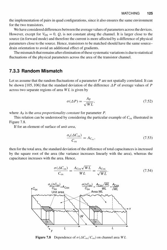
MATCHING 125
the implementation of pairs in quad configurations, since it also ensures the same environment
for the two transistors.
We have considered differences between the average values of parameters across the devices.
However, except for VDS = 0, Qi is not constant along the channel. It is larger close to the
source (in forward mode) and therefore the current is more affected by a difference of physical
parameters close to the source. Hence, transistors to be matched should have the same source–
drain orientation to avoid an additional effect of gradients.
The mismatch that remains after elimination of these systematic variations is due to statistical
fluctuations of the physical parameters across the area of the transistor channel.
7.3.3 Random Mismatch
Let us assume that the random fluctuations of a parameter P are not spatially correlated. It can
be shown [105, 106] that the standard deviation of the difference ΔP of average values of P
across two separate regions of area W L is given by
σ (ΔP) =AP√W L
, (7.52)
where AP is the area proportionality constant for parameter P.
This relation can be understood by considering the particular example of Cox illustrated in
Figure 7.8.
If for an element of surface of unit area,
σu(ΔCox)
Cox
= ACox, (7.53)
then for the total area, the standard deviation of the difference of total capacitances is increased
by the square root of the area (the variance increases linearly with the area), whereas the
capacitance increases with the area. Hence,
σ (ΔCox)
Cox
=ACox
√W L
W L=
ACox√W L
. (7.54)
y
x
1 1
Cox=ACox
su(∆Cox)
CoxUnit area Area WL
ACox
WL
WLs(∆Cox)
Cox WL
ACox==
W
L L
Figure 7.8 Dependence of σ (ΔCox/Cox) on channel area W L
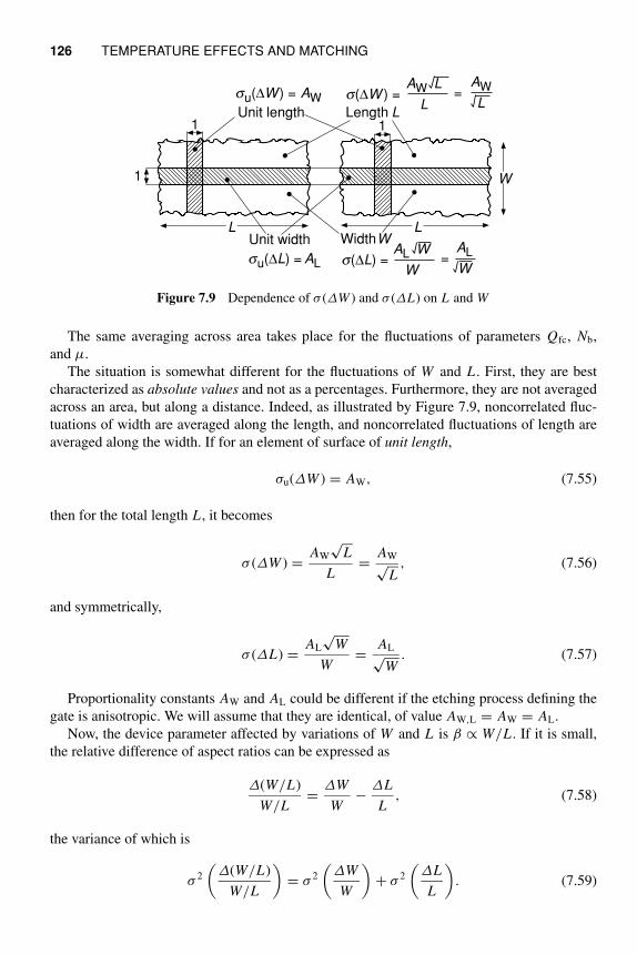
126 TEMPERATURE EFFECTS AND MATCHING
W
LL
1 1
1
Unit length
su(∆W ) = AW
Unit width
su(∆L) = AL
Length L
s(∆W ) = =AW L
L
AW
L
Width W
s(∆L) = =AL W
W
AL
W
Figure 7.9 Dependence of σ (ΔW ) and σ (ΔL) on L and W
The same averaging across area takes place for the fluctuations of parameters Qfc, Nb,
and μ.
The situation is somewhat different for the fluctuations of W and L . First, they are best
characterized as absolute values and not as a percentages. Furthermore, they are not averaged
across an area, but along a distance. Indeed, as illustrated by Figure 7.9, noncorrelated fluc-
tuations of width are averaged along the length, and noncorrelated fluctuations of length are
averaged along the width. If for an element of surface of unit length,
σu(ΔW ) = AW, (7.55)
then for the total length L , it becomes
σ (ΔW ) =AW
√L
L=
AW√L
, (7.56)
and symmetrically,
σ (ΔL) =AL
√W
W=
AL√W
. (7.57)
Proportionality constants AW and AL could be different if the etching process defining the
gate is anisotropic. We will assume that they are identical, of value AW,L = AW = AL.
Now, the device parameter affected by variations of W and L is β ∝ W/L . If it is small,
the relative difference of aspect ratios can be expressed as
Δ(W/L)
W/L=
ΔW
W−
ΔL
L, (7.58)
the variance of which is
σ 2
(Δ(W/L)
W/L
)
= σ 2
(ΔW
W
)
+ σ 2
(ΔL
L
)
. (7.59)
MATCHING 127
Introducing (7.56) and (7.57) with AW = AL = AW,L yields
σ 2
(Δ(W/L)
W/L
)
=A2
W,L
W L
(1
L+
1
W
)
=A2
W,L
(W L)3/2
(√
W
L+
√
L
W
)
. (7.60)
The mismatch of W/L decreases faster than that of other relevant parameters when the
channel area is increased while keeping W/L constant. Its contribution to the mismatch of β
can therefore be made negligible by increasing W L . Moreover, its variance is minimum for a
square channel and increases with approximately the square root of the aspect ratio.
It should be emphasized that the proportionality constant AP was defined by comparing the
mismatch of two identical transistors (same nominal values of W and L). If one transistor is
infinitely large, then the mismatch is reduced by√
2. Hence, for two transistors of different
W L , it becomes
σ (ΔP) =AP√
2
√
1
W1L1
+1
W2L2
. (7.61)
Now, except for very large dimensions, the mismatch of two transistors of different sizes
is increased by side effects. Hence, a ratio M/N of β ∝ W/L is best obtained by a series
and/or parallel combination of M and N identical elementary transistors of same W and L .
The resulting mismatch is then given by
σ (ΔP) =AP√2W L
√
1
M+
1
N. (7.62)
Using the variances defined above for the (uncorrelated) mismatches of the basic parameters,
the variances of the three device parameters are obtained directly from (7.38), (7.39), and (7.40):
σ 2(ΔVT0) = [(2n0 − 1)UT + (n0 − 1)Ψ0]2 σ 2
(ΔNb
Nb
)
+[
Qfc
Cox
− 2(n0 − 1)Ψ0
]2
σ 2
(ΔCox
Cox
)
+(
Qfc
Cox
)2
σ 2
(ΔQfc
Qfc
)
, (7.63)
σ 2(Δn) = (n0 − 1)2
[(1
2−
UT
Ψ0
)2
σ 2
(ΔNb
Nb
)
+ σ 2
(ΔCox
Cox
)]
(7.64)
σ 2
(Δβ
β
)
= σ 2
(Δμ
μ
)
+ σ 2
(ΔCox
Cox
)
+ σ 2
[Δ(W L)
W/L
]
. (7.65)
According to (7.52), the same equations are applicable if each σ (P) is replaced by the
corresponding area proportionality constant AP.
Now, the mismatch of these three parameters is possibly correlated through ΔCox and ΔNb.
In order to evaluate the practical importance of this correlation, an example is illustrated in
Figure 7.10. The mismatch of drain currents and gate voltages is calculated for three cases,
with the same realistic values of σ (ΔVT0) and σ (Δβ
β).
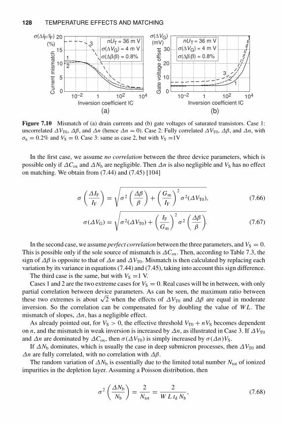
128 TEMPERATURE EFFECTS AND MATCHING
0
5
10
15
1 102 10410–2
Inversion coefficient IC
(%)
Curr
ent m
ism
atc
h
nUT = 36 m V
s(∆VG) = 4 m V
s(∆b/b) = 0.8%
0
10
20
30
1 102 10410–2
Inversion coefficient IC
(mV)
Gate
voltage o
ffset
2
1
3
1
32
(a) (b)
s(∆VG)s(∆IF/IF)nUT = 36 m V
s(∆VG) = 4 m V
s(∆b/b) = 0.8%
20
Figure 7.10 Mismatch of (a) drain currents and (b) gate voltages of saturated transistors. Case 1:
uncorrelated ΔVT0, Δβ, and Δn (hence Δn = 0). Case 2: Fully correlated ΔVT0, Δβ, and Δn, with
σn = 0.2% and VS = 0. Case 3: same as case 2, but with VS =1V
In the first case, we assume no correlation between the three device parameters, which is
possible only if ΔCox and ΔNb are negligible. Then Δn is also negligible and VS has no effect
on matching. We obtain from (7.44) and (7.45) [104]
σ
(ΔIF
IF
)
=
√
σ 2
(Δβ
β
)
+(
Gm
IF
)2
σ 2(ΔVT0), (7.66)
σ (ΔVG) =
√
σ 2(ΔVT0) +(
IF
Gm
)2
σ 2
(Δβ
β
)
. (7.67)
In the second case, we assume perfect correlation between the three parameters, and VS = 0.
This is possible only if the sole source of mismatch is ΔCox. Then, according to Table 7.3, the
sign of Δβ is opposite to that of Δn and ΔVT0. Mismatch is then calculated by replacing each
variation by its variance in equations (7.44) and (7.45), taking into account this sign difference.
The third case is the same, but with VS =1 V.
Cases 1 and 2 are the two extreme cases for VS = 0. Real cases will be in between, with only
partial correlation between device parameters. As can be seen, the maximum ratio between
these two extremes is about√
2 when the effects of ΔVT0 and Δβ are equal in moderate
inversion. So the correlation can be compensated for by doubling the value of W L . The
mismatch of slopes, Δn, has a negligible effect.
As already pointed out, for VS > 0, the effective threshold VT0 + nVS becomes dependent
on n, and the mismatch in weak inversion is increased by Δn, as illustrated in Case 3. If ΔVT0
and Δn are dominated by ΔCox, then σ (ΔVT0) is simply increased by σ (Δn)VS.
If ΔNb dominates, which is usually the case in deep submicron processes, then ΔVT0 and
Δn are fully correlated, with no correlation with Δβ.
The random variation of ΔNb is essentially due to the limited total number Ntot of ionized
impurities in the depletion layer. Assuming a Poisson distribution, then
σ 2
(ΔNb
Nb
)
=2
Ntot
=2
W L td Nb
, (7.68)
MATCHING 129
where the factor 2 comes from the fact that we compare two transistors. The thickness td of
the depletion layer given by 3.26 can be evaluated at Ψs = Ψ0:
td =
√
2Ψ0ǫsi
q Nb
, (7.69)
resulting in
σ
(ΔNb
Nb
)
=1
√W L
· 4
√
2q
Ψ0ǫsi Nb
. (7.70)
Now, if ΔNb dominates and if Ψ0 ≫ UT, then 7.63 can be approximated by
σ (ΔVT0) = (n0 − 1)Ψ0σ
(ΔNb
Nb
)
=Γb
2
√
Ψ0 · σ
(ΔNb
Nb
)
(7.71)
where n0 has been replaced by its expression (3.73). By introducing σ (ΔNb
Nb) given by (7.70)
and Γb given by (3.30), we obtain the area proportionality constant for threshold mismatch
AVT0=
√W Lσ (ΔVT0) =
1
Cox
4
√
q3ǫsi NbΨ0
2. (7.72)
Now, the comparison of (7.64) with (7.63) for Ψ0 ≫ UT shows that if mismatch is dominated
by ΔNb, then
An=
√W L σ (Δn) =
AVT0
2Ψ0
=1
2Cox
4
√
q3ǫsi Nb
2Ψ 30
. (7.73)
It should be pointed out that (7.72) and (7.73) are slightly pessimistic, since td in (7.69)
is evaluated at Ψs = Ψ0, which is its minimum value. For VS > 0, Ψs ≥ Ψ0 + VS and td is
increased, thereby decreasing ΔNb/Nb according to (7.68) [107]. However, this small effect
can be neglected as compared to the global effect of increasing VS. Indeed, since ΔVT0 and
Δn are fully correlated by their common origin ΔNb, the mismatch of effective gate threshold
voltages VT0 + nVS is
σ (VT0 + nVS) = σ (VT0)
(
1 +VS
2Ψ0
)
, (7.74)
This expression describes explicitly, for the particular case of ΔVT0 dominated by ΔNb, the
effect of VS illustrated by curve 3 in Figure 7.10. An important consequence of this increase of
mismatch due to VS > 0 appears in a differential pair: its input offset voltage is increased by
the nonzero source voltage if the two paired transistors are not put in a separate well connected
to their sources.

Part II
The Extended Charge-BasedModel
This second part models several nonideal effects that should be added to the core model
developed in Part I, in order to best describe modern MOS transistors, in particular those
realized in deep submicron processes. Chapter 8 focuses on effects that already affect long-
channel devices, whereas Chapter 9 specifically adresses the short-channel effects. Finally,
the passive devices that must be added to account for the extrinsic part of the transistor are
modeled in Chapter 10.
Charge-Based MOS Transistor Modeling: The EKV Model for Low-Power and RF IC Design C. Enz and E. VittozC© 2006 John Wiley & Sons, Ltd.

8 Nonideal Effects Relatedto the Vertical Dimension
All the nonideal effects discussed in this chapter remain compatible with expression (4.40) of
the drain current. Hence, they do not affect the fundamental property of symmetry discussed
in Section (4.5). Section 8.2 shows the impact of the mobility reduction resulting from a large
gate voltage. Current and tranconductances are reduced, but their ratio is not much affected.
Section 8.3 investigates the case of nonuniform vertical doping, with a detailed analysis of
two particular profiles. The following sections examine the consequences of the very high
substrate doping and very thin gate oxide introduced in aggressively scaled-down processes.
Polysilicon gate depletion discussed in Section 8.4 can be accounted for by a reduction of
specific charge and current, by an increase of the slope factor for voltages, and by an increased
threshold voltage. Band gap widening due to quantum effects is examined in Section 8.5. It
has the same qualitative effect on charge, current, and threshold voltage as polydepletion, with
which it is usually combined. Gate leakage current due to tunneling through a very thin oxide
is analyzed in Section 8.6. Negligible if the oxide is thicker than 3 nm, this current increases
by more than a factor 10 for each 0.2 nm of thickness reduction.
8.1 INTRODUCTION
In this chapter we still consider a long and wide channel that is homogeneous in the x direction
(along the channel). As demonstrated in Section 4.5, the fundamental property of symmetry is
not affected; hence, the drain current can still be decomposed in a forward component IF and a
reverse component IR. We will separately discuss the main nonideal effects that are related to
the vertical dimension, and show how they can be accounted for by modifying the basic model
presented in Part I.
8.2 MOBILITY REDUCTION DUE TO THE VERTICAL FIELD
In a MOS transistor, the current flows very close to the silicon surface. As a consequence, the
mobility of current carriers is lower than deep inside the substrate (typically two to three times
Charge-Based MOS Transistor Modeling: The EKV Model for Low-Power and RF IC Design C. Enz and E. VittozC© 2006 John Wiley & Sons, Ltd.
134 NONIDEAL EFFECTS RELATED TO THE VERTICAL DIMENSION
lower), due to various scattering mechanisms [67]. This mobility is further reduced if the
vertical field Ez becomes too large. This field dependent mobility can be approximated by [1]
µz =µ0
1 + Eeff/E0
, (8.1)
where µ0 is the low-field surface mobility, E0∼= 4 × 10⁷ V/m the electric field at which
the mobility starts to decrease significantly, and Eeff the average field in the inversion layer,
approximated by
Eeff =1
2[Ezs + Ezb] , (8.2)
where Ezs and Ezb are the values of the vertical electric field at the surface and just below the
inversion layer respectively.
According to the Gauss law illustrated by Figure 3.2,
Ezs = −(Qi + Qb)/ǫsi and Ezb = −Qb/ǫsi. (8.3)
Hence
Eeff = −1
ǫsi
(
Qb +Qi
2
)
. (8.4)
Introducing (8.4) in expression (8.1) of the field-dependent mobility yields
μz =μ0
1 − Qb+Qi/2
ǫsi E0
=μ0
1 + θ (qb + qi/2). (8.5)
In the second form, the charge is normalized to Qspec defined by (3.42) and θ depends on
E0 according to
θ =Qspec
ǫsi E0
=2nCoxUT
ǫsi E0
. (8.6)
The mobility reduction is a function of the inverted charge density Qi and of the bulk
depletion charge density Qb. The latter is given by (3.55) as a linearized function of Qi, where
the slope factor n can be replaced by its value nw given by (3.68) resulting in
qb =ψp − qi
1 + 2γb
√ψp
. (8.7)
Introducing this result in (8.5) provides the variation of mobility with mobile charge qi:
μz
μ0
=1
k1qi + k2
, (8.8)
where
k1 = θ
(
1
2−
1
1 + 2γb
√ψp
)
and k2 = 1 +θψp
1 + 2γb
√ψp
. (8.9)
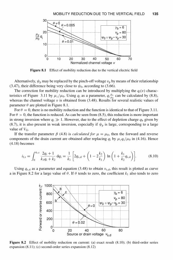
MOBILITY REDUCTION DUE TO THE VERTICAL FIELD 135
0 10 20 30 40 50 60 70
10
20mzm0
qi
30
0
q = 0q = 0.005
q = 0.01
Normalized channel voltage v
gb = 6
vp = 80
y0 ≅ yp– vp = 30
Figure 8.1 Effect of mobility reduction due to the vertical electric field
Alternatively, ψp may be replaced by the pinch-off voltage vp by means of their relationship
(3.47), their difference being very close to ψ0, according to (3.66).
The correction for mobility reduction can be introduced by multiplying the qi(v) charac-
teristics of Figure 3.11 by μz/μ0. Using qi as a parameter, qiμz
μ0can be calculated by (8.8),
whereas the channel voltage v is obtained from (3.48). Results for several realistic values of
parameter θ are plotted in Figure 8.1.
For θ = 0, there is no mobility reduction and the function is identical to that of Figure 3.11.
For θ > 0, the function is reduced. As can be seen from (8.5), this reduction is more important
in strong inversion where qi ≫ 1. However, due to the effect of depletion charge qb given by
(8.7), it is also present in weak inversion, especially if ψp is large, corresponding to a large
value of VG.
If the transfer parameter β (4.8) is calculated for μ = μ0, then the forward and reverse
components of the drain current are obtained after replacing qi by μzqi/μ0 in (4.16). Hence
(4.18) becomes
if,r =∫ qs,d
0
2qi + 1
k1qi + k2
dqi =1
k1
[
2qs,d +(
1 − 2k2
k1
)
ln
(
1 +k1
k2
qs,d
)]
. (8.10)
Using qs,d as a parameter and equation (3.48) to obtain vs,d, this result is plotted as curve
a in Figure 8.2 for a large value of θ . If θ tends to zero, the coefficient k1 also tends to zero
080604020
200
400
800
1000
600
0
q =0
q = 0.02
a
b
c
if,r
vs,dSource or drain voltage
Fo
rwa
rd o
r re
ve
rse
cu
rre
nt
gb = 6
vp = 80
y0 ≅ yp–vp = 30
Figure 8.2 Effect of mobility reduction on current: (a) exact result (8.10); (b) third-order series
expansion (8.11); (c) second-order series expansion (8.12)
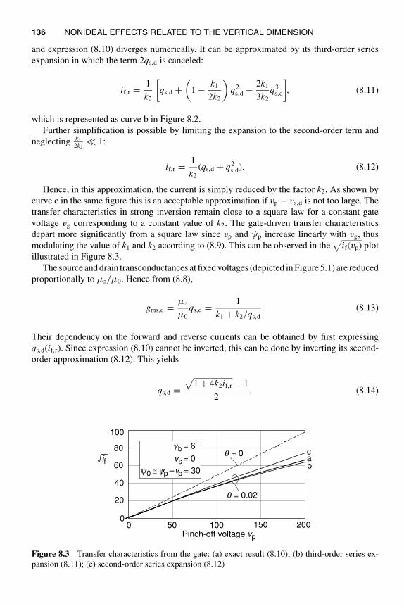
136 NONIDEAL EFFECTS RELATED TO THE VERTICAL DIMENSION
and expression (8.10) diverges numerically. It can be approximated by its third-order series
expansion in which the term 2qs,d is canceled:
if,r =1
k2
[
qs,d +(
1 −k1
2k2
)
q2s,d −
2k1
3k2
q3s,d
]
, (8.11)
which is represented as curve b in Figure 8.2.
Further simplification is possible by limiting the expansion to the second-order term and
neglecting k1
2k2≪ 1:
if,r =1
k2
(qs,d + q2s,d). (8.12)
Hence, in this approximation, the current is simply reduced by the factor k2. As shown by
curve c in the same figure this is an acceptable approximation if vp − vs,d is not too large. The
transfer characteristics in strong inversion remain close to a square law for a constant gate
voltage vg corresponding to a constant value of k2. The gate-driven transfer characteristics
depart more significantly from a square law since vp and ψp increase linearly with vg, thus
modulating the value of k1 and k2 according to (8.9). This can be observed in the√
if(vp) plot
illustrated in Figure 8.3.
The source and drain transconductances at fixed voltages (depicted in Figure 5.1) are reduced
proportionally to μz/μ0. Hence from (8.8),
gms,d =μz
μ0
qs,d =1
k1 + k2/qs,d
. (8.13)
Their dependency on the forward and reverse currents can be obtained by first expressing
qs,d(if,r). Since expression (8.10) cannot be inverted, this can be done by inverting its second-
order approximation (8.12). This yields
qs,d =√
1 + 4k2if,r − 1
2, (8.14)
0 50 100 150 2000
20
40
60
80
100
q = 0
q = 0.02
ab
c
Pinch-off voltage vp
if
gb = 6
vs = 0
y0 ≅ yp –vp = 30
Figure 8.3 Transfer characteristics from the gate: (a) exact result (8.10); (b) third-order series ex-
pansion (8.11); (c) second-order series expansion (8.12)
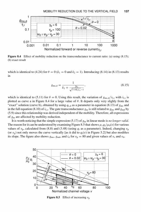
MOBILITY REDUCTION DUE TO THE VERTICAL FIELD 137
0.01
0.1
1
1 10 100 10000.10.010.001
q = 0.02
q = 0
b
a
Normalized forward or reverse current if,r
gms,dif,r
1/ if,r
gb = 6
vp = 100
y0 ≅ yp–vp = 30
Figure 8.4 Effect of mobility reduction on the transconductance to current ratio: (a) using (8.15);
(b) exact result
which is identical to (4.24) for θ = 0 (k1 = 0 and k2 = 1). Introducing (8.14) in (8.13) results
in
gms,d =1
k1 + 2k2√1+4k2if,r−1
, (8.15)
which is identical to (5.11) for θ = 0. Using this result, the variation of gms,d/ if,r with if,r is
plotted as curve a in Figure 8.4 for a large value of θ . It departs only very slighly from the
“exact” solution (curve b), obtained by using qs,d as a parameter in equation (8.13) of gms and
in the full equation (8.10) of if,r. The gate transconductance gm is still related to gms and gmd by
(5.9) since this relationship was derived independent of the mobility. Therefore, all expressions
of gm are affected by mobility reduction.
It is worth noticing that the simple expression (5.17) of gm in linear mode is no longer valid.
The reason for it can be understood by examining Figure 8.5 that shows μzqi/μ0(v) for various
values of vp, calculated from (8.8) and (3.48) (using qi as a parameter). Indeed, changing vp
(or vg) not only moves the curve vertically [as it did to qi(v) in Figure 5.2] but also modifies
its slope. The figure also shows gms, gmd, and id for vp = 80 and given values of vs and vd.
0
50
0 10020 40 60 80
10
20
30
40
Normalized channel voltage v
q = 0q = 0.02
v g -in
crease
s
gb = 6
y0 ≅ yp– vp= 30
vs
gms
vd
gmd
gm
id
vp= 80
mzm0
q i
Figure 8.5 Effect of increasing vp
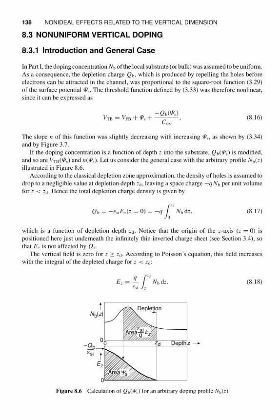
138 NONIDEAL EFFECTS RELATED TO THE VERTICAL DIMENSION
8.3 NONUNIFORM VERTICAL DOPING
8.3.1 Introduction and General Case
In Part I, the doping concentration Nb of the local substrate (or bulk) was assumed to be uniform.
As a consequence, the depletion charge Qb, which is produced by repelling the holes before
electrons can be attracted in the channel, was proportional to the square-root function (3.29)
of the surface potential Ψs. The threshold function defined by (3.33) was therefore nonlinear,
since it can be expressed as
VTB = VFB + Ψs +−Qb(Ψs)
Cox
, (8.16)
The slope n of this function was slightly decreasing with increasing Ψs, as shown by (3.34)
and by Figure 3.7.
If the doping concentration is a function of depth z into the substrate, Qb(Ψs) is modified,
and so are VTB(Ψs) and n(Ψs). Let us consider the general case with the arbitrary profile Nb(z)
illustrated in Figure 8.6.
According to the classical depletion zone approximation, the density of holes is assumed to
drop to a negligible value at depletion depth zd, leaving a space charge −q Nb per unit volume
for z < zd. Hence the total depletion charge density is given by
Qb = −ǫsi Ez(z = 0) = −q
∫ zd
0
Nb dz, (8.17)
which is a function of depletion depth zd. Notice that the origin of the z-axis (z = 0) is
positioned here just underneath the infinitely thin inverted charge sheet (see Section 3.4), so
that Ez is not affected by Qi.
The vertical field is zero for z ≥ zd. According to Poisson’s equation, this field increases
with the integral of the depleted charge for z < zd:
Ez =q
ǫsi
∫ zd
z
Nb dz. (8.18)
zd00
0
Depth z
DepletionNb(z)
εsiq EzArea
Ez
YsArea
–Qbεsi
Figure 8.6 Calculation of Qb(Ψs) for an arbitrary doping profile Nb(z)
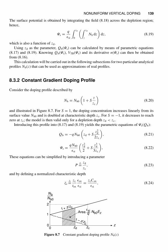
NONUNIFORM VERTICAL DOPING 139
The surface potential is obtained by integrating the field (8.18) across the depletion region;
hence,
Ψs =q
ǫsi
∫ zd
0
(∫ zd
z
Nb dz
)
dz, (8.19)
which is also a function of zd.
Using zd as the parameter, Qb(Ψs) can be calculated by means of parametric equations
(8.17) and (8.19). Knowing Qb(Ψs), VTB(Ψs) and its derivative n(Ψs) can then be obtained
from (8.16).
This calculation will be carried out in the following subsections for two particular analytical
profiles Nb(z) that can be used as approximations of real profiles.
8.3.2 Constant Gradient Doping Profile
Consider the doping profile described by
Nb = Nb0
(
1 + Sz
zc
)
(8.20)
and illustrated in Figure 8.7. For S = 1, the doping concentration increases linearly from its
surface value Nb0 and is doubled at characteristic depth zc. For S = −1, it decreases to reach
zero at zc; the model is then valid only for a depletion depth zd < zc.
Introducing this profile into (8.17) and (8.19) yields the parametric equations of Ψs(Qb):
Qb = −q Nb0
(
zd + Sz2
d
2zc
)
, (8.21)
Ψs =q Nb0
ǫsi
(z2
d
2+ S
z3d
3zc
)
, (8.22)
These equations can be simplified by introducing a parameter
P=
zd
zc
, (8.23)
and by defining a normalized characteristic depth
ζc=
zc
tox
ǫox
ǫsi
=zcCox
ǫsi
, (8.24)
0
1
2
0 zcz
zd
1+ z/zc
1 – z/zc
εsiq
Nb0EzArea
NbNb0
Figure 8.7 Constant gradient doping profile Nb(z)
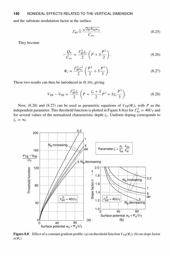
140 NONIDEAL EFFECTS RELATED TO THE VERTICAL DIMENSION
and the substrate modulation factor at the surface
Γb0=
√2q Nb0ǫsi
Cox
. (8.25)
They become
−Qb
Cox
=Γ 2
b0ζc
2
(
P + SP2
2
)
, (8.26)
Ψs =Γ 2
b0ζ2c
2
(P2
2+ S
P3
3
)
. (8.27)
These two results can then be introduced in (8.16), giving
VTB − VFB =Γ 2
b0ζc
2
(
P +ζc + S
2P2 + Sζc
P3
3
)
. (8.28)
Now, (8.28) and (8.27) can be used as parametric equations of VTB(Ψs), with P as the
independent parameter. This threshold function is plotted in Figure 8.8(a) for Γ 2bo = 40UT and
for several values of the normalized characteristic depth ζc. Uniform doping corresponds to
ζc = ∞.
Parameter zzctox
εoxεsi
=
5
1.0
1.2
1.4
1.6
1.8
2.0
0 40 80
0.2
1
5oo
Slo
pe
fa
cto
r n
0
40
80
120
160
2000.2
5
1
5
VTB –VFBUT
Th
resh
old
fu
nctio
n
(a)0 40 80
ys = Ys/UTSurface potential
oo
Gb0 = 40UT2
Nb increasing
Nb decreasing
Nb increasing
Nb decreasing
(b)
Gb0 = 40UT2
ys = Ys/UTSurface potential
Figure 8.8 Effect of a constant gradient profile: (a) on threshold function VTB(Ψs); (b) on slope factor
n(Ψs)
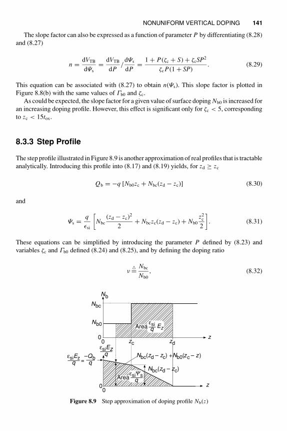
NONUNIFORM VERTICAL DOPING 141
The slope factor can also be expressed as a function of parameter P by differentiating (8.28)
and (8.27)
n =dVTB
dΨs
=dVTB
dP/
dΨs
dP=
1 + P(ζc + S) + ζcSP2
ζc P(1 + SP). (8.29)
This equation can be associated with (8.27) to obtain n(Ψs). This slope factor is plotted in
Figure 8.8(b) with the same values of Γb0 and ζc.
As could be expected, the slope factor for a given value of surface doping Nb0 is increased for
an increasing doping profile. However, this effect is significant only for ζc < 5, corresponding
to zc < 15tox.
8.3.3 Step Profile
The step profile illustrated in Figure 8.9 is another approximation of real profiles that is tractable
analytically. Introducing this profile into (8.17) and (8.19) yields, for zd ≥ zc
Qb = −q [Nb0zc + Nbc(zd − zc)] (8.30)
and
Ψs =q
ǫsi
[
Nbc
(zd − zc)2
2+ Nbczc(zd − zc) + Nb0
z2c
2
]
. (8.31)
These equations can be simplified by introducing the parameter P defined by (8.23) and
variables ζc and Γb0 defined (8.24) and (8.25), and by defining the doping ratio
ν=
Nbc
Nb0
, (8.32)
00
z
Nb
Nb0
Nbc
z
zd
εsiq
EzArea
εsiYsqArea
00
zcεsiEz
q
Nbc(zd – zc)
Nbc(zd – zc) +Nb0(zc – z)εsiEzq =
–Qbq
Figure 8.9 Step approximation of doping profile Nb(z)
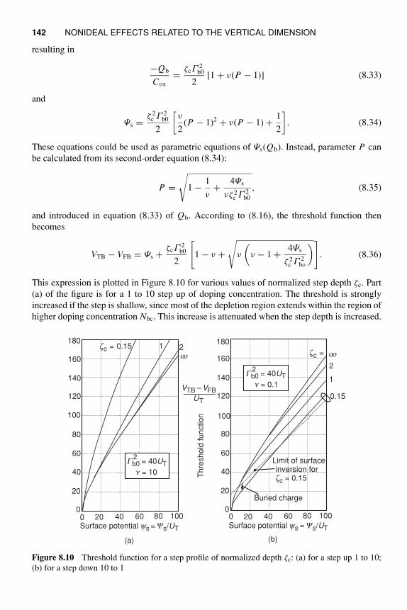
142 NONIDEAL EFFECTS RELATED TO THE VERTICAL DIMENSION
resulting in
−Qb
Cox
=ζcΓ
2b0
2[1 + ν(P − 1)] (8.33)
and
Ψs =ζ 2
c Γ 2b0
2
[ν
2(P − 1)2 + ν(P − 1) +
1
2
]
. (8.34)
These equations could be used as parametric equations of Ψs(Qb). Instead, parameter P can
be calculated from its second-order equation (8.34):
P =
√
1 −1
ν+
4Ψs
νζ 2c Γ 2
b0
, (8.35)
and introduced in equation (8.33) of Qb. According to (8.16), the threshold function then
becomes
VTB − VFB = Ψs +ζcΓ
2b0
2
[
1 − ν +
√
ν
(
ν − 1 +4Ψs
ζ 2c Γ 2
bo
)]
. (8.36)
This expression is plotted in Figure 8.10 for various values of normalized step depth ζc. Part
(a) of the figure is for a 1 to 10 step up of doping concentration. The threshold is strongly
increased if the step is shallow, since most of the depletion region extends within the region of
higher doping concentration Nbc. This increase is attenuated when the step depth is increased.
zc = 210.15
Gb0 = 40UT2
n = 10
0 20 40 60 80 1000
20
40
60
80
100
120
140
160
180
Surface potential ys = Ys/UT
oo
(a)
Th
resh
old
fu
nctio
n
0 20 40 60 80 1000
20
40
60
80
120
140
160
Surface potential ys = Ys/UT
Gb0 = 40UT2
n = 0.1
zc =
2
1
0.15
Limit of surfaceinversion forzc = 0.15
oo
100
180
(b)
Buried charge
VTB – VFBUT
Figure 8.10 Threshold function for a step profile of normalized depth ζc: (a) for a step up 1 to 10;
(b) for a step down 10 to 1
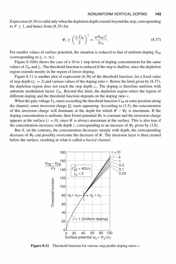
NONUNIFORM VERTICAL DOPING 143
Expression (8.36) is valid only when the depletion depth extends beyond the step, corresponding
to P ≥ 1, and hence from (8.35) for
Ψs ≥(
ζcΓb0
2
)2
=q Nb0z2
c
2ǫsi
. (8.37)
For smaller values of surface potential, the situation is reduced to that of uniform doping Nb0
(corresponding to ζc = ∞).
Figure 8.10(b) shows the case of a 10 to 1 step down of doping concentration for the same
values of Γb0 and ζc. The threshold function is reduced if the step is shallow, since the depletion
region extends mostly in the region of lower doping.
Figure 8.11 is another plot of expression (8.36) of the threshold function, for a fixed value
of step depth (ζc = 2) and various values of the doping ratio ν. Below the limit given by (8.37),
the depletion region does not reach the step depth zc. The doping is therefore uniform with
substrate modulation factor Γb0. Beyond this limit, the depletion region enters the region of
different doping and the threshold function depends on the doping ratio ν.
When the gate voltage VG starts exceeding the threshold function VTB at some position along
the channel, some inversion charge Qi starts appearing. According to (3.5), the concentration
of this inversion charge will dominate at the depth for which Ψ − ΦF is maximum. If the
doping concentration is uniform, then Fermi potential ΦF is constant and the inversion charge
appears at the surface (z = 0), since Ψ is always maximum at the surface. This is also true if
the concentration increases with depth z, corresponding to an increase of ΦF given by (3.8).
But if, on the contrary, the concentration decreases steeply with depth, the corresponding
decrease of ΦF can possibly overcome the decrease of Ψ . The inversion layer is then created
below the surface, resulting in what is called a buried channel.
0 20 40 60 80 1000
20
40
60
80
n = 1 (Uniform doping)
zd > zczd < zc
100
120
140
160
180
Surface potential ys = Ys/UT
Gb0 = 40UT2
zc = 2
VTB –VFBUT
Th
resh
old
fu
nctio
n
n =10
310.30.10.03
Figure 8.11 Threshold function for various step profile doping ratios ν
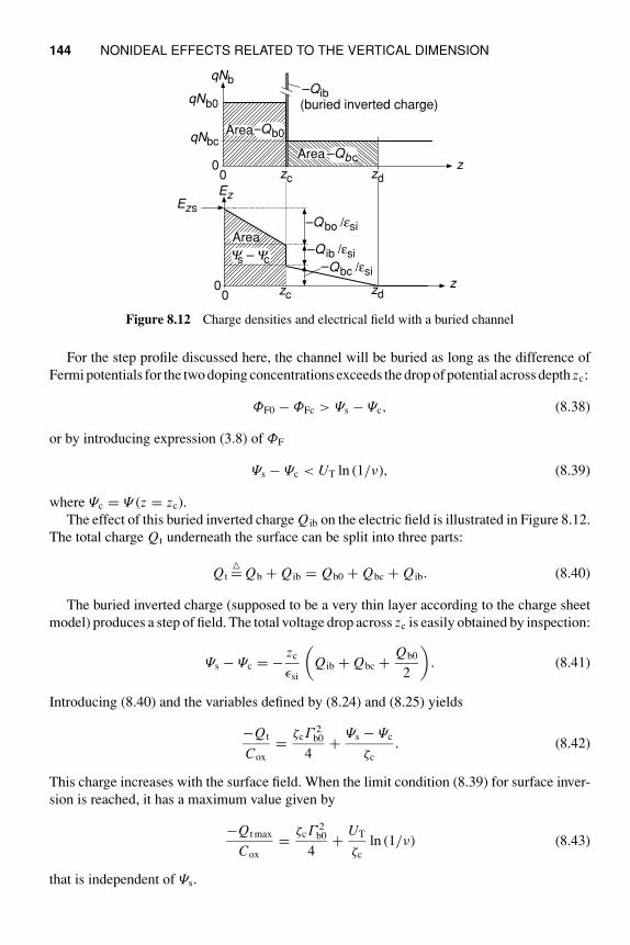
144 NONIDEAL EFFECTS RELATED TO THE VERTICAL DIMENSION
00
z
qNb
qNb0
qNbc
z
zd
–Qb0Area
00
zc
Area –Qbc
–Qib(buried inverted charge)
EzEzs
Area
Ys – Yc
–
–
–
Qbo /esi
Q ib /εsi
Qbc /εsi
zdzc
Figure 8.12 Charge densities and electrical field with a buried channel
For the step profile discussed here, the channel will be buried as long as the difference of
Fermi potentials for the two doping concentrations exceeds the drop of potential across depth zc:
ΦF0 − ΦFc > Ψs − Ψc, (8.38)
or by introducing expression (3.8) of ΦF
Ψs − Ψc < UT ln (1/ν), (8.39)
where Ψc = Ψ (z = zc).
The effect of this buried inverted charge Qib on the electric field is illustrated in Figure 8.12.
The total charge Qt underneath the surface can be split into three parts:
Qt= Qb + Qib = Qb0 + Qbc + Qib. (8.40)
The buried inverted charge (supposed to be a very thin layer according to the charge sheet
model) produces a step of field. The total voltage drop across zc is easily obtained by inspection:
Ψs − Ψc = −zc
ǫsi
(
Qib + Qbc +Qb0
2
)
. (8.41)
Introducing (8.40) and the variables defined by (8.24) and (8.25) yields
−Qt
Cox
=ζcΓ
2b0
4+
Ψs − Ψc
ζc
. (8.42)
This charge increases with the surface field. When the limit condition (8.39) for surface inver-
sion is reached, it has a maximum value given by
−Qt max
Cox
=ζcΓ
2b0
4+
UT
ζc
ln (1/ν) (8.43)
that is independent of Ψs.
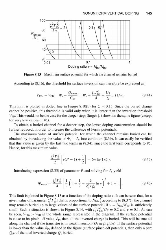
NONUNIFORM VERTICAL DOPING 145
20
40
60
80
100
0.31 0.13z Gb0
UT
22
=c
10
YsmaxUT
0.01 0.1
Doping ratio n = Nbc /Nbo
1
Figure 8.13 Maximum surface potential for which the channel remains buried
According to (8.16), the threshold for surface inversion can therefore be expressed as
VTBs − VFB = Ψs −Qt max
Cox
= Ψs +ζcΓ
2b0
4+
UT
ζc
ln (1/ν). (8.44)
This limit is plotted in dotted line in Figure 8.10(b) for ζc = 0.15. Since the buried charge
cannot be positive, this threshold is valid only when it is larger than the inversion threshold
VTB. This would not be the case for the deeper steps (larger ζc) shown in the same figure (except
for very low values of Ψs).
To obtain a buried channel for a deeper step, the lower doping concentration should be
further reduced, in order to increase the difference of Fermi potentials.
The maximum value of surface potential for which the channel remains buried can be
obtained by introducing the value of Ψs − Ψc into condition (8.39). It can easily be verified
that this value is given by the last two terms in (8.34), since the first term correponds to Ψc.
Hence, for this maximum value,
ζ 2c Γ 2
b0
2
[
ν(P − 1) +1
2
]
= UT ln (1/ζc). (8.45)
Introducing expression (8.35) of parameter P and solving for Ψs yield
Ψs max =ζ 2
c Γ 2b0
4
[
1
ν
(
ν −1
2−
2
ζ 2c Γ 2
b0
ln ν
)2
+ 1 − ν
]
. (8.46)
This limit is plotted in Figure 8.13 as a function of the doping ratio ν. It can be seen that, for a
given value of parameter ζ 2c Γ 2
b0 [that is proportional to Nb0z2c according to (8.37)], the channel
may remain buried up to large values of the surface potential if ν = Nbc/Nb0 is sufficiently
small. Such a situation is shown in Figure 8.14, with ζ 2c Γ 2
b0/UT = 0.2 and ν = 0.1. As can
be seen, VTBs > VTB in the whole range represented in the diagram. If the surface potential
is close to its pinch-off value ΨP, then all the inverted charge is buried. This will be true all
along the channel if the transistor is in weak inversion (Qi negligible). If the surface potential
is lower than the value ΨPs defined in the figure (surface pinch-off potential), then only a part
Qib of the total inverted charge Qi buried.
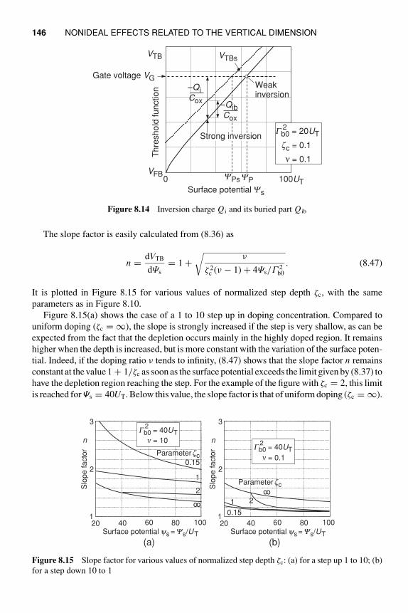
146 NONIDEAL EFFECTS RELATED TO THE VERTICAL DIMENSION
Gb0 = 20UT2
zc = 0.1
n = 0.1
0
Surface potential Ys
Th
resh
old
fu
nctio
n
100UT
VFB
VTB
Gate voltage VGWeakinversion
–QiCox
VTBs
YPs YP
–QibCox
Strong inversion
Figure 8.14 Inversion charge Qi and its buried part Qib
The slope factor is easily calculated from (8.36) as
n =dVTB
dΨs
= 1 +√
ν
ζ 2c (ν − 1) + 4Ψs/Γ
2b0
. (8.47)
It is plotted in Figure 8.15 for various values of normalized step depth ζc, with the same
parameters as in Figure 8.10.
Figure 8.15(a) shows the case of a 1 to 10 step up in doping concentration. Compared to
uniform doping (ζc = ∞), the slope is strongly increased if the step is very shallow, as can be
expected from the fact that the depletion occurs mainly in the highly doped region. It remains
higher when the depth is increased, but is more constant with the variation of the surface poten-
tial. Indeed, if the doping ratio ν tends to infinity, (8.47) shows that the slope factor n remains
constant at the value 1 + 1/ζc as soon as the surface potential exceeds the limit given by (8.37) to
have the depletion region reaching the step. For the example of the figure with ζc = 2, this limit
is reached for Ψs = 40UT. Below this value, the slope factor is that of uniform doping (ζc = ∞).
20 40 60 80 1001
2
3
Surface potential ys = Ys/UT
Slo
pe facto
r
n
Gb0 = 40UT2
n = 10
2
1
0.15
oo
Parameter zc
(a)
20 40 60 80 1001
2
3
Surface potential ys= Ys/UT
Slo
pe facto
r
nGb0 = 40UT
2
n = 0.1
oo
1
0.15
2
Parameter zc
(b)
Figure 8.15 Slope factor for various values of normalized step depth ζc: (a) for a step up 1 to 10; (b)
for a step down 10 to 1
NONUNIFORM VERTICAL DOPING 147
Slo
pe
fa
cto
r
n
Surface potential ys = Ys/UT
1
2
20 40 60 80 100
Gb0 = 40UT2
zc = 2
103
1
0.3
0.1
0.03
n = oo
Figure 8.16 Slope factor for various step profile doping ratios ν
Figure 8.15(b) shows the case of a 10 to 1 step down of doping concentration. The slope
factor is lowered by a shallow step (most of the depletion occurring in the lightly doped region).
However, it increases very steeply when the surface potential is reduced and approaches the
limit given by (8.37).
In Figure 8.16, the slope factor is plotted for ζc = 2 and various values of the doping ratio. It
shows again that when the depletion region reaches the step, the way n varies with the surface
potential strongly depends on the doping ratio.
8.3.4 Effect on the Basic Model
The nonuniformity of vertical doping affects only the shape of the threshold function, and
hence the slope factor and the threshold voltage. Therefore, the whole model derived in Part
I is still applicable with new values of these parameters. The threshold voltage at equilibrium
VT0 was defined by (3.58) as the value of the threshold function VTB for V = 0 (channel at
equilibrium). Hence, from (3.56),
VT0 = VTB(Ψs = Ψ0), (8.48)
where Ψ0 is given by (3.66) with ΦF calculated from (3.8) with Nb = Nb0.
The effect of the constant gradient profile as illustrated in Figure 8.8 can be approximated
by fitting the substrate modulation factor Γb of a uniform profile. Both the threshold voltage
and the slope factor are increased (decreased) if the doping is increasing (decreasing) with
depth.
For the step profile approximation, the threshold voltage can be expressed explicitly from
(8.36):
VT0 = VFB + Ψ0 +ζcΓ
2b0
2
[
1 − ν +
√
ν
(
ν − 1 +4Ψ0
ζ 2c Γ 2
b0
)]
. (8.49)
The pinch-off potential ΨP was defined in Section 3.5 as the value of surface potential for
which the inverted charge is zero; that is,
ΨP = Ψs(VG = VTB), (8.50)
148 NONIDEAL EFFECTS RELATED TO THE VERTICAL DIMENSION
100UT
VT01
VT02
VFB0
VFB + 100UT
0Slo
pe n 1
Slo
pe n 2
Y0
Ys
V
zc Gb02
2
VTB
zd > zczd
< zc
Gb0 = 40UT
zc = 2.5
2
n = 0.01
Figure 8.17 Dual slope threshold function
and is related to the pinch-off voltage by VP = ΨP − Ψ0 according to (3.66). But no simple
relation exists here to replace expression (3.37) of ΨP. Instead, VP can be approximated by
(3.63).
For a given value of surface doping (and hence of Γb0), the effect of a step profile depends on
the step depth zc and the step doping ratio ν = Nbc/Nb0. A step up (ν > 1) can only increase VT0
and n, but it improves the linearity of threshold function VTB and hence reduces the variation
of n with the surface potential, as shown by Figure 8.11 and Figure 8.16.
A step down (ν < 1) can only reduce VT0 and n, but it may result in an abrupt change of
slope at the limit given by (8.37), as illustrated in Figure 8.16. Therefore, a dual slope threshold
model might be needed as illustrated by the example of Figure 8.17.
Threshold VT01 and slope n1 correspond to the region of uniform doping. They are thus
given by (3.58) and (3.34) with Γb = Γb0 [or by (8.49) and (8.47) with ν = 1]. According
to Figure 8.16, the evaluation of n2 should be made by (8.47) with a value of Ψs sufficiently
larger than ζcΓ2
b0/2. Inspection of Figure 8.17 shows that the second threshold voltage can be
calculated by
VT02 = VT01 + (n1 − n2)[(ζcΓb0/2)2 − Ψ0
]. (8.51)
8.4 POLYSILICON DEPLETION
8.4.1 Definition of the Effect
In the basic model discussed in Part I, we have assumed a constant potential VG throughout the
thickness of the gate electrode, which would always be true if the gate material was a metal.
It is still true for a (poly)silicon gate, as long as the thickness of the layer of positive charge
QG (that is concentrated at the lower face of the gate electrode) is so small that the voltage
ΔΨg across it is negligible. If the gate is N-type, we can assume that a positive gate charge QG
is entirely produced by the depletion layer created at the lower face of the gate. If the gate is
P-type, this depletion layer can possibly create a negative gate charge QG.
POLYSILICON DEPLETION 149
To calculate ΔΨg, we can further assume that the model of equations (3.29) and (3.30)
giving
Ψs =(
Qb
ΓbCox
)2
with Γb =√
2q Nbǫsi
Cox
(8.52)
for the monocrystalline bulk with doping concentration Nb remains valid for the polysilicon
gate with concentration Ng. Then by analogy [45]
ΔΨg = ±(
Qg
ΓgCox
)2
for ± Qg > 0, (8.53)
where
Γg =√
2q Ngǫsi
Cox
(8.54)
is the gate modulation factor. The positive sign in (8.53) corresponds to the positive voltage
drop created through the depletion layer of an N-type gate (for Qg > 0), whereas the negative
sign corresponds to the negative voltage drop that might eventually be created in the depletion
layer of a P-type gate (for Qg < 0).
Comparing (8.52) with (8.53) and (8.54) shows that ΔΨg remains negligible as long as
Ng/Nb ≫ (Qg/Qb)2.
Now, while scaling-down process dimensions, Nb must be increased whereas Ng cannot
be increased proportionally. Hence ΔΨg may become nonnegligible, especially if Qg is made
much larger than −Qb by a large value of inverted charge −Qi (very strong inversion).
Although the original definition of the fixed interface charge Qfc in Section 2.2 included
the equivalent effect of the charge distributed throughout the oxide thickness, let us assume
here that all this charge is physically located at the silicon-oxide interface. Hence, because of
the overall charge neutrality
Qg = −(Qb + Qi + Qfc). (8.55)
The depletion voltage at the gate then becomes
ΔΨg = ±(
Qb + Qi + Qfc
ΓgCox
)2
. (8.56)
8.4.2 Effect on the Mobile Inverted Charge
This voltage drop ΔΨg given by (8.56) must be subtracted from VG in the voltage to charge
relation (3.19). This yields
±1
Γ 2g
(Qi + Qb + Qfc
Cox
)2
−Qi + Qb + Qfc
Cox
− (VG − Φms − Ψs) = 0. (8.57)
The mobile charge density Qi is then obtained by first solving this second-order equation
150 NONIDEAL EFFECTS RELATED TO THE VERTICAL DIMENSION
in (Qi + Qb + Qfc)/Cox, giving
Qi + Qb + Qfc = Cox
[
±Γ 2
g
2
(
1 −√
1 ±4
Γ 2g
(VG − Ψs − Φms)
)]
. (8.58)
Then, by introducing expression (3.29) of Qb,
Qi = Cox
[
Γb
√
Ψs ±Γ 2
g
2
(
1 −√
1 ±4
Γ 2g
(VG − Ψs − Φms)
)]
− Qfc. (8.59)
8.4.3 Slope Factors and Pinch-Off Surface Potential
We can now compare (8.59) with (3.32), to which it reduces for Γg very large. As a first remark,
Φms and Qfc cannot be lumped anymore into a flat-band voltage VFB. But most important is
the fact that Qi is no longer proportional to the difference between the gate voltage VG and a
threshold function VTB(Ψs). The diagram of Figure 3.7 is therefore no longer applicable. As
a consequence, the slope of Qi
Cox(Ψs) is no longer identical to that of VG(ΨP). Therefore, the
single slope factor n introduced in Part I must be replaced by two distinct slope factors:
nv =dVG
dΨP
=dVG
dVP
and nq =dQi/Cox
dΨs
. (8.60)
In order to obtain an expression for nv, we have to first calculate VG(ΨP) that replaces (3.33)
plotted in Figure 3.7. Introducing Qi = 0 and Ψs = ΨP in (8.59) results in
VG = Φms −Qfc
Cox
+ ΨP + Γb
√
ΨP ±1
Γ 2g
(Qfc
Cox
− Γb
√
ΨP
)2
, (8.61)
which reduces to expression (3.33) of VTB(Ψs) for Γg very large.
It must be reminded that, according to (3.66), ΨP is related to the pinch-off voltage VP by
ΨP = VP + Ψ0 = VP + 2ΦF + Vsh. (8.62)
Equation (8.61) is plotted in Figure 8.18 for particular values of γb = Γb/UT and γg =Γg/UT, and for five different values of fixed charge Qfc/Cox ranging from −40 to 40.
Now, polydepletion is possible only if the charge QG on the gate is positive for an N-type
gate or negative for a P-type gate. At pinch-off Qi = 0, hence from (8.55) polydepletion at
pinch-off occurs only for
±(Qb + Qfc) < 0. (8.63)
By introducing expression (3.29) of Qb with Ψs = ΨP, this condition becomes
±(
Γb
√Ψ P −
Qfc
Cox
)
> 0. (8.64)
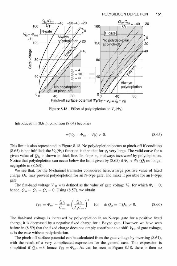
POLYSILICON DEPLETION 151
No polydepletionat pinch-off
40
80
0
–40 –20–40 –20
0 40 800
120
160
N-gateVG – Fms
UT
Slo
pe n v
=Qfc /Cox
UT
40
Gate
voltage
20
Alwayspolydepletion
0
40
80
120
0
40
20
P-gate
Alwayspolydepletion
Slo
pe n v
No polydepletionat pinch-off
0 40 80
160–40 –20
Pinch-off surface potential YP/UT = yp ≅ vp + y0
=Qfc/Cox
UT
gb
= 4gg = 10gg = •
Figure 8.18 Effect of polydepletion on VG(Ψp)
Introduced in (8.61), condition (8.64) becomes
±(VG − Φms − ΨP) > 0. (8.65)
This limit is also represented in Figure 8.18. No polydepletion occurs at pinch-off if condition
(8.65) is not fulfilled; the VG(ΨP) function is then that for γg very large. The valid curve for a
given value of Qfc is shown in thick line. Its slope nv is always increased by polydepletion.
Notice that polydepletion can occur below the limit given by (8.65) if Ψs < ΨP (Qi no longer
negligible in (8.63)).
We see that, for the N-channel transistor considered here, a large positive value of fixed
charge Qfc may prevent polydepletion for an N-type gate, and make it possible for an P-type
gate.
The flat-band voltage VFB was defined as the value of gate voltage VG for which Ψs = 0;
hence, Qsi = Qb + Qi = 0. Using (8.57), we obtain
VFB = Φms −Qfc
Cox
±(
Qfc
ΓgCox
)2
for ± Qg = ∓Qfc > 0. (8.66)
The flat-band voltage is increased by polydepletion in an N-type gate for a positive fixed
charge; it is decreased by a negative fixed charge for a P-type gate. However, we have seen
before in (8.59) that the fixed charge does not simply contribute to a shift VFB of gate voltage,
as is the case without polydepletion.
The pinch-off surface potential can be calculated from the gate voltage by inverting (8.61),
with the result of a very complicated expression for the general case. This expression is
simplified if Qfc = 0 hence VFB = Φms. As can be seen in Figure 8.18, there is then no
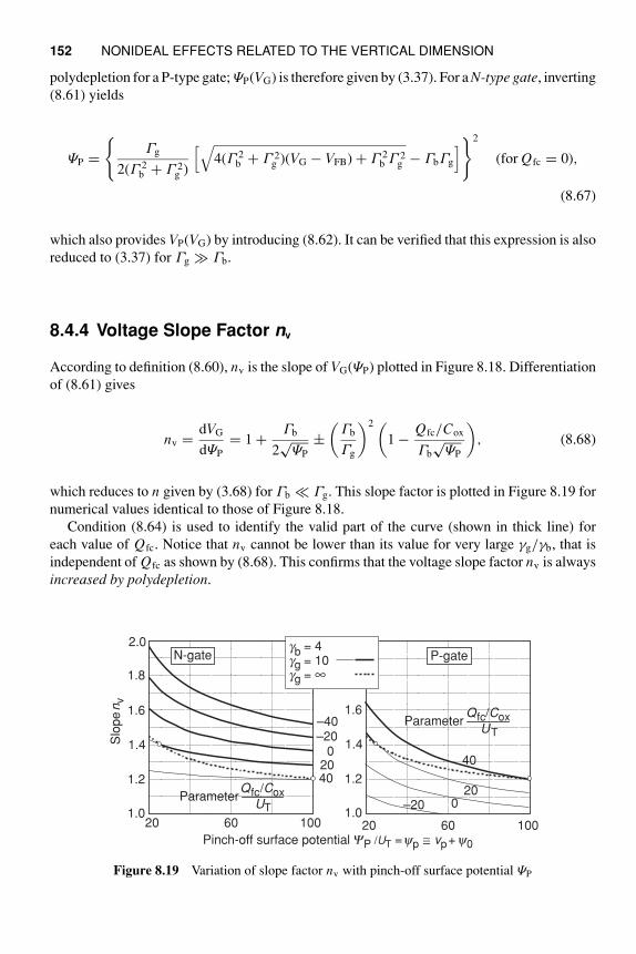
152 NONIDEAL EFFECTS RELATED TO THE VERTICAL DIMENSION
polydepletion for a P-type gate; ΨP(VG) is therefore given by (3.37). For a N-type gate, inverting
(8.61) yields
ΨP =
Γg
2(Γ 2b + Γ 2
g )
[√
4(Γ 2b + Γ 2
g )(VG − VFB) + Γ 2b Γ 2
g − ΓbΓg
]2
(for Qfc = 0),
(8.67)
which also provides VP(VG) by introducing (8.62). It can be verified that this expression is also
reduced to (3.37) for Γg ≫ Γb.
8.4.4 Voltage Slope Factor nv
According to definition (8.60), nv is the slope of VG(ΨP) plotted in Figure 8.18. Differentiation
of (8.61) gives
nv =dVG
dΨP
= 1 +Γb
2√
ΨP
±(
Γb
Γg
)2(
1 −Qfc/Cox
Γb
√ΨP
)
, (8.68)
which reduces to n given by (3.68) for Γb ≪ Γg. This slope factor is plotted in Figure 8.19 for
numerical values identical to those of Figure 8.18.
Condition (8.64) is used to identify the valid part of the curve (shown in thick line) for
each value of Qfc. Notice that nv cannot be lower than its value for very large γg/γb, that is
independent of Qfc as shown by (8.68). This confirms that the voltage slope factor nv is always
increased by polydepletion.
–40–20
02040
40
200–20
1.0
1.2
1.4
1.6
1.8
2.0
1.0
1.2
1.4
1.6
1.8
2.0
20 60 100
Pinch-off surface potential YP /UT =yp ≅ vp+ y0
Slo
pe n
v
N-gate P-gategb = 4gg = 10gg = •
ParameterQfc/Cox
UT
ParameterQfc/Cox
UT
20 60 100
Figure 8.19 Variation of slope factor nv with pinch-off surface potential ΨP
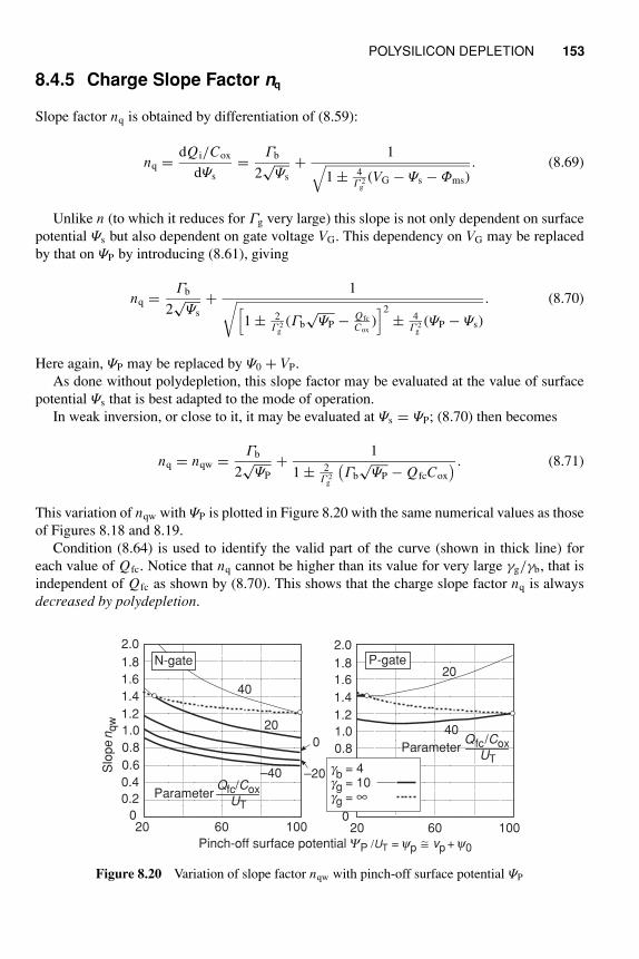
POLYSILICON DEPLETION 153
8.4.5 Charge Slope Factor nq
Slope factor nq is obtained by differentiation of (8.59):
nq =dQi/Cox
dΨs
=Γb
2√
Ψs
+1
√
1 ± 4Γ 2
g(VG − Ψs − Φms)
. (8.69)
Unlike n (to which it reduces for Γg very large) this slope is not only dependent on surface
potential Ψs but also dependent on gate voltage VG. This dependency on VG may be replaced
by that on ΨP by introducing (8.61), giving
nq =Γb
2√
Ψs
+1
√[
1 ± 2Γ 2
g(Γb
√ΨP − Qfc
Cox)]2
± 4Γ 2
g(ΨP − Ψs)
. (8.70)
Here again, ΨP may be replaced by Ψ0 + VP.
As done without polydepletion, this slope factor may be evaluated at the value of surface
potential Ψs that is best adapted to the mode of operation.
In weak inversion, or close to it, it may be evaluated at Ψs = ΨP; (8.70) then becomes
nq = nqw =Γb
2√
ΨP
+1
1 ± 2Γ 2
g
(Γb
√ΨP − QfcCox
) . (8.71)
This variation of nqw with ΨP is plotted in Figure 8.20 with the same numerical values as those
of Figures 8.18 and 8.19.
Condition (8.64) is used to identify the valid part of the curve (shown in thick line) for
each value of Qfc. Notice that nq cannot be higher than its value for very large γg/γb, that is
independent of Qfc as shown by (8.70). This shows that the charge slope factor nq is always
decreased by polydepletion.
40
20
0
2.0
1.0
0.2
0.4
0.6
0.8
1.2
1.4
1.6
1.8
0
2.0
1.0
0.2
0.4
0.6
0.8
1.2
1.4
1.6
1.8
Pinch-off surface potential YP /UT = yp ≅ vp + y0
20 60 100 20 60 100
Slo
pe n
qw
40
20
0
–20–40 gb
= 4gg = 10gg = •
N-gate P-gate
ParameterQfc/Cox
UT
ParameterQfc/Cox
UT
Figure 8.20 Variation of slope factor nqw with pinch-off surface potential ΨP
154 NONIDEAL EFFECTS RELATED TO THE VERTICAL DIMENSION
For strong inversion, a better evaluation of nq given by (8.70) may be at Ψs = Ψ0 + VP/2,
resulting in
nq = nqs =Γb
2√
Ψ0 + VP/2+
1√[
1 ± 2Γ 2
g(Γb
√Ψ0 + VP − Qfc
Cox)]2
± 2Γ 2
gVP
. (8.72)
8.4.6 Effect on Qi(V), Currents, and Transconductances
The continuous expression of V (Qi) (3.48) and its approximations (3.49) and (3.50) in weak
and strong inversion remain valid if n is replaced by nq given by (8.70) in the normaliza-
tion of Qi. Hence the specific charge (3.42) used for this normalization must be replaced
by
Qspec = −2nqUTCox, (8.73)
The same remark applies to the normalized drain current and its forward and reverse com-
ponents derived in Sections 4.4.1 and 4.4.6 provided that the specific current is redefined
as
Ispec = 2nqβU 2T. (8.74)
In particular, results (4.25) and (4.39) and the corresponding characteristics in Figure 4.5
remain unchanged.
As explained in Chapter 5, the source transconductance Gms is proportional to the density
QiS of mobile charge at the source (in normalized form, gms = qs). Symmetrically, the drain
transconductance Gmd is proportional to the density QiD of mobile charge at the drain (in nor-
malized form, gmd = qd). Therefore, all expressions of Gms,d as functions of IF,R or VP − VS,D
remain valid, provided n is replaced by nq. The specific conductance used for normalization
becomes
Gspec = 2nqβUT. (8.75)
Now, since by definition (8.60) the slope of VG(VP) is nv, the gate transconductance is given
by
Gm =Gms − Gmd
nv
, (8.76)
instead of (5.9).
It can be pointed out that, since polydepletion reduces nq, it reduces Gms,d (except in
weak inversion at a fixed current). Since it increases nv, Gm is further reduced proportio-
nally.
The effect of polydepletion can be combined with that of mobility reduction by simply
applying relations (8.73) to (8.76) in the analysis of Section 8.2.
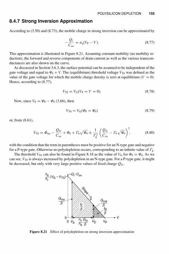
POLYSILICON DEPLETION 155
8.4.7 Strong Inversion Approximation
According to (3.50) and (8.73), the mobile charge in strong inversion can be approximated by
−Qi
Cox
= nq(VP − V ). (8.77)
This approximation is illustrated in Figure 8.21. Assuming constant mobility (no mobility re-
duction), the forward and reverse components of drain current as well as the various transcon-
ductances are also shown on the curve.
As discussed in Section 3.6.3, the surface potential can be assumed to be independent of the
gate voltage and equal to Ψ0 + V. The (equilibrium) threshold voltage VT0 was defined as the
value of the gate voltage for which the mobile charge density is zero at equilibrium (V = 0).
Hence, according to (8.77),
VT0 = VG(VP = V = 0). (8.78)
Now, since VP = ΨP − Ψ0 (3.66), then
VT0 = VG(ΨP = Ψ0) (8.79)
or, from (8.61),
VT0 = Φms −Qfc
Cox
+ Ψ0 + Γb
√
Ψ0 ±1
Γ 2g
(Qfc
Cox
− Γb
√
Ψ0
)2
, (8.80)
with the condition that the term in parentheses must be positive for an N-type gate and negative
for a P-type gate. Otherwise no polydepletion occurs, corresponding to an infinite value of Γg.
The threshold VT0 can also be found in Figure 8.18 as the value of VG for ΨP = Ψ0. As we
can see, VT0 is always increased by polydepletion in an N-type gate. For a P-type gate, it might
be decreased, but only with very large positive values of fixed charge Qfc.
Slope –
nq
nq
nv(VG –VT0)
00 VPVDVS
V
–Q i /Cox
Gms
bGmd
b
nvnq
Gm
b
IRb
IFb
Figure 8.21 Effect of polydepletion on strong inversion approximation
156 NONIDEAL EFFECTS RELATED TO THE VERTICAL DIMENSION
According to (8.60), nv is the slope of VG(VP). Furthermore, VT0 = VG(VP = 0) as expressed
by (8.78). Therefore, the pinch-off voltage can be approximated by
VP =VG − VT0
nv
. (8.81)
This approximation can be used to obtain VP = ΨP − Ψ0, instead of (8.67), which was anyhow
valid only for Qfc = 0.
Introducing (8.81) into (8.77) provides a simple expression of Qi(VG, V ):
−Qi
Cox
= nq
(VG − VT0
nv
− V
)
. (8.82)
Hence, a variation ΔVG of gate voltage results in a vertical shiftnq
nvΔVG < ΔVG of Qi/Cox(V )
as depicted in Figure 8.21. This explains the value of gate transconductance in linear mode
Gm =nq
nv
β(VD − VS). (8.83)
8.5 BAND GAP WIDENING
8.5.1 Introduction
In modern deep submicron processes, the oxide thickness is reduced to very small values,
whereas the gate voltage is not reduced proportionally. The electric field at the silicon surface
is therefore increased, and confined states originating from a quantum treatment can no longer
be ignored. As a consequence, the highest allowed energy level for holes is slightly below the
top of the valence band by an amount qΔΨv, and the lowest allowed energy level for electrons
is slightly above the bottom of the conduction band by an amount qΔΨc. With this band gap
widening effect, expression (3.5) of the concentration of electrons must be modified to [47,108]
np = ni expΨ − ΦF − V − ΔΨc
UT
. (8.84)
In inversion, it can be assumed that ΔΨc is primarily a function of the effective vertical field
at the silicon-oxide interface. Since this field is proportional to the charge in the silicon, ΔΨc
can be expressed as [47]
ΔΨc = Aqm(−Qb − ηQi)2/3. (8.85)
The physical constant Aqm is given by
Aqm =(
1
2m∗q
)1/3(9
16
h
ǫsi
)2/3
= 3.53Vm4/3
A2/3s2/3, (8.86)
where h is the Planck’s constant and m∗ is the effective mass of the electron (equal to 98% of
its free mass for <100> substrate orientation).
BAND GAP WIDENING 157
The constant η accounts for the effective value of the surface field. Its value is typically 3/4,
but it can be used as a fitting parameter.
For a uniformly doped substrate, the depletion charge linearized around its value at Ψs = ΨP
is given by (3.54) and is not affected by possible polydepletion. It can further be related to the
inverted charge by means of (3.39) (with n = nq to account for polydepletion), resulting in
Qb = −ΓbCox
√
ΨP −n − 1
nq
Qi, (8.87)
where n is given by (3.34) and nq is given by (8.70). Introducing this expression of Qb(Qi)
into (8.85) gives
ΔΨc = Aqm
[
ΓbCox
√
ΨP +(
1 − n
nq
+ η
)
(−Qi)
]2/3
, (8.88)
or, with the normalized variables defined by (3.41), (3.43), and (8.73),
δψc =AqmC2/3
ox
U1/3T
[
γb
√
ψp + (1 − n + ηnq)2qi
]2/3
, (8.89)
which is plotted in Figure 8.22 for several values of the pinch-off potential, η = 3/4, and
nq = n = nw given by (3.68).
As given by (8.88), ΔΨc is a nonlinear function of both ΨP and Qi. It can be linearized with
respect to Qi around Qi = 0, giving
ΔΨc = Aqm
(
ΓbCox
√
ΨP
)2/3
︸ ︷︷ ︸
ΔΨcP
+2
3AqmCox(ηnq + 1 − n)
(
ΓbCox
√
ΨP
)−1/3
︸ ︷︷ ︸
δqm
−Qi
nqCox
, (8.90)
0 50
yp = 20
yp = 60
yp = 100
010 20 30 40
∆yc
Cox UT2/3 –1/3
Aqm
qi
gb
= 40210
20
30
Figure 8.22 Dependency of band gap widening Δψc on inverted charge qi; linear approximation in
dotted line
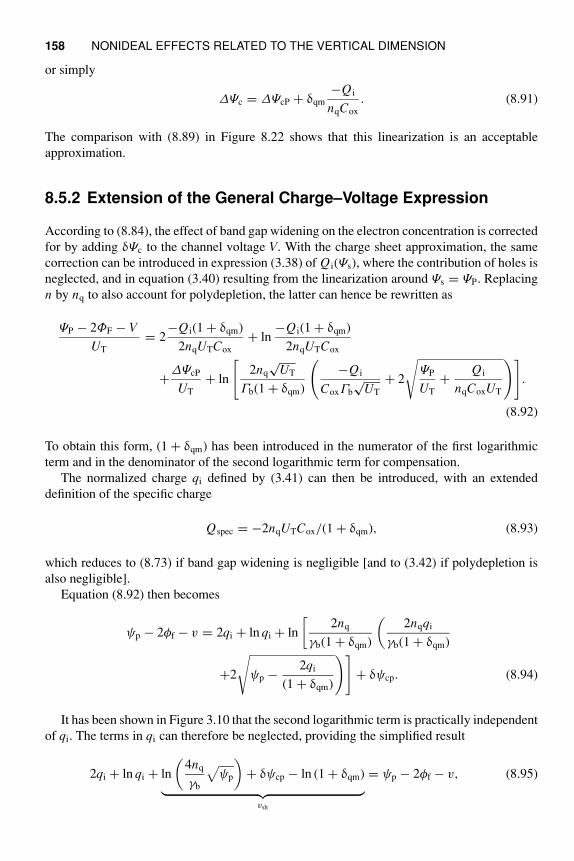
158 NONIDEAL EFFECTS RELATED TO THE VERTICAL DIMENSION
or simply
ΔΨc = ΔΨcP + δqm
−Qi
nqCox
. (8.91)
The comparison with (8.89) in Figure 8.22 shows that this linearization is an acceptable
approximation.
8.5.2 Extension of the General Charge–Voltage Expression
According to (8.84), the effect of band gap widening on the electron concentration is corrected
for by adding δΨc to the channel voltage V. With the charge sheet approximation, the same
correction can be introduced in expression (3.38) of Qi(Ψs), where the contribution of holes is
neglected, and in equation (3.40) resulting from the linearization around Ψs = ΨP. Replacing
n by nq to also account for polydepletion, the latter can hence be rewritten as
ΨP − 2ΦF − V
UT
= 2−Qi(1 + δqm)
2nqUTCox
+ ln−Qi(1 + δqm)
2nqUTCox
+ΔΨcP
UT
+ ln
[
2nq
√UT
Γb(1 + δqm)
(
−Qi
CoxΓb
√UT
+ 2
√
ΨP
UT
+Qi
nqCoxUT
)]
.
(8.92)
To obtain this form, (1 + δqm) has been introduced in the numerator of the first logarithmic
term and in the denominator of the second logarithmic term for compensation.
The normalized charge qi defined by (3.41) can then be introduced, with an extended
definition of the specific charge
Qspec = −2nqUTCox/(1 + δqm), (8.93)
which reduces to (8.73) if band gap widening is negligible [and to (3.42) if polydepletion is
also negligible].
Equation (8.92) then becomes
ψp − 2φf − v = 2qi + ln qi + ln
[2nq
γb(1 + δqm)
(2nqqi
γb(1 + δqm)
+2
√
ψp −2qi
(1 + δqm)
)]
+ δψcp. (8.94)
It has been shown in Figure 3.10 that the second logarithmic term is practically independent
of qi. The terms in qi can therefore be neglected, providing the simplified result
2qi + ln qi + ln
(4nq
γb
√
ψp
)
+ δψcp − ln (1 + δqm)
︸ ︷︷ ︸
vsh
= ψp − 2φf − v, (8.95)
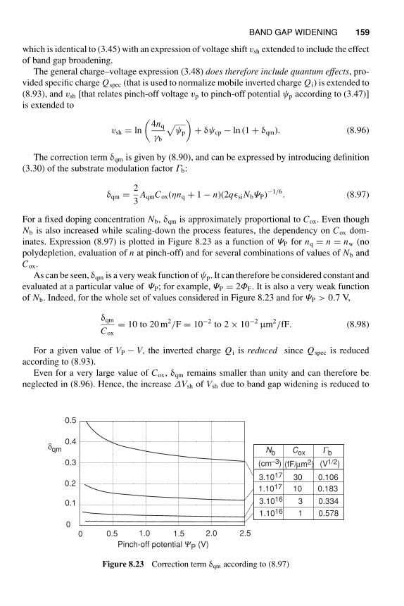
BAND GAP WIDENING 159
which is identical to (3.45) with an expression of voltage shift vsh extended to include the effect
of band gap broadening.
The general charge–voltage expression (3.48) does therefore include quantum effects, pro-
vided specific charge Qspec (that is used to normalize mobile inverted charge Qi) is extended to
(8.93), and vsh [that relates pinch-off voltage vp to pinch-off potential ψp according to (3.47)]
is extended to
vsh = ln
(4nq
γb
√
ψp
)
+ δψcp − ln (1 + δqm). (8.96)
The correction term δqm is given by (8.90), and can be expressed by introducing definition
(3.30) of the substrate modulation factor Γb:
δqm =2
3AqmCox(ηnq + 1 − n)(2qǫsi NbΨP)−1/6. (8.97)
For a fixed doping concentration Nb, δqm is approximately proportional to Cox. Even though
Nb is also increased while scaling-down the process features, the dependency on Cox dom-
inates. Expression (8.97) is plotted in Figure 8.23 as a function of ΨP for nq = n = nw (no
polydepletion, evaluation of n at pinch-off) and for several combinations of values of Nb and
Cox.
As can be seen, δqm is a very weak function of ψp. It can therefore be considered constant and
evaluated at a particular value of ΨP; for example, ΨP = 2ΦF. It is also a very weak function
of Nb. Indeed, for the whole set of values considered in Figure 8.23 and for ΨP > 0.7 V,
δqm
Cox
= 10 to 20 m2/F = 10−2 to 2 × 10⁻² µm2/fF. (8.98)
For a given value of VP − V, the inverted charge Qi is reduced since Qspec is reduced
according to (8.93).
Even for a very large value of Cox, δqm remains smaller than unity and can therefore be
neglected in (8.96). Hence, the increase ΔVsh of Vsh due to band gap widening is reduced to
Nb Cox Gb
(cm–3) (fF/µm2) (V1/2)
3.1017 30 0.106
1.1017 10 0.183
3.1016 3 0.334
1.1016 1 0.578
0 0.5 1.0 1.5 2.0 2.5
Pinch-off potential YP (V)
0
0.1
0.2
0.3
0.4
0.5
δqm
Figure 8.23 Correction term δqm according to (8.97)
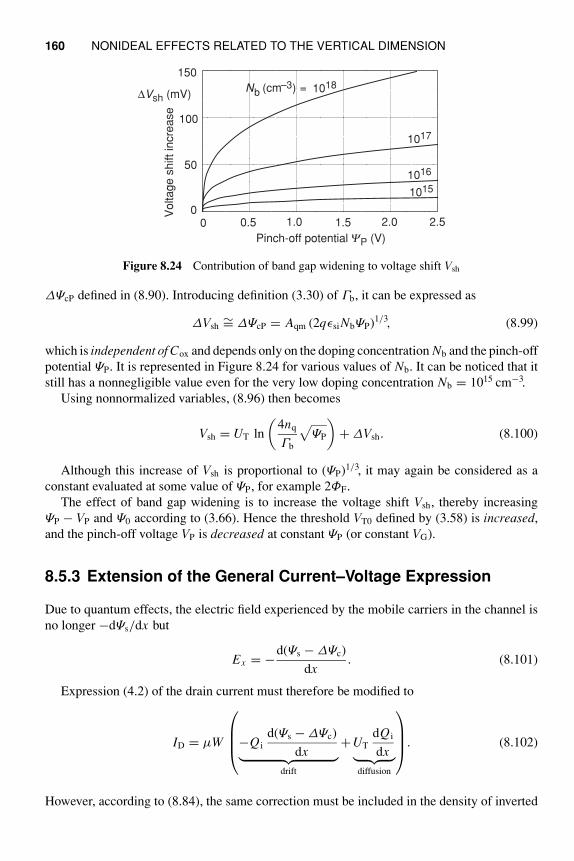
160 NONIDEAL EFFECTS RELATED TO THE VERTICAL DIMENSION
0 0.5 1.0 1.5 2.0 2.5
Pinch-off potential YP (V)
0
50
100
150
∆Vsh (mV)Nb (cm–3) = 1018
1017
1016
1015
Voltage s
hift in
cre
ase
Figure 8.24 Contribution of band gap widening to voltage shift Vsh
ΔΨcP defined in (8.90). Introducing definition (3.30) of Γb, it can be expressed as
ΔVsh∼= ΔΨcP = Aqm (2qǫsi NbΨP)1/3, (8.99)
which is independent of Cox and depends only on the doping concentration Nb and the pinch-off
potential ΨP. It is represented in Figure 8.24 for various values of Nb. It can be noticed that it
still has a nonnegligible value even for the very low doping concentration Nb = 1015 cm−3.
Using nonnormalized variables, (8.96) then becomes
Vsh = UT ln
(4nq
Γb
√
ΨP
)
+ ΔVsh. (8.100)
Although this increase of Vsh is proportional to (ΨP)1/3, it may again be considered as a
constant evaluated at some value of ΨP, for example 2ΦF.
The effect of band gap widening is to increase the voltage shift Vsh, thereby increasing
ΨP − VP and Ψ0 according to (3.66). Hence the threshold VT0 defined by (3.58) is increased,
and the pinch-off voltage VP is decreased at constant ΨP (or constant VG).
8.5.3 Extension of the General Current–Voltage Expression
Due to quantum effects, the electric field experienced by the mobile carriers in the channel is
no longer −dΨs/dx but
Ex = −d(Ψs − ΔΨc)
dx. (8.101)
Expression (4.2) of the drain current must therefore be modified to
ID = μW
⎛
⎜⎜⎝
−Qi
d(Ψs − ΔΨc)
dx︸ ︷︷ ︸
drift
+ UT
dQi
dx︸ ︷︷ ︸
diffusion
⎞
⎟⎟⎠
. (8.102)
However, according to (8.84), the same correction must be included in the density of inverted
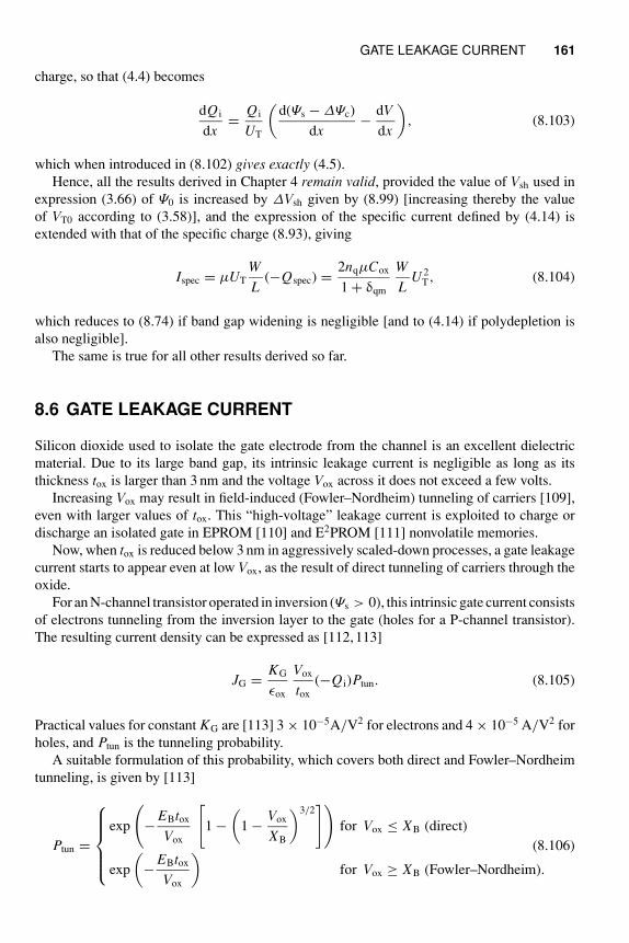
GATE LEAKAGE CURRENT 161
charge, so that (4.4) becomes
dQi
dx=
Qi
UT
(d(Ψs − ΔΨc)
dx−
dV
dx
)
, (8.103)
which when introduced in (8.102) gives exactly (4.5).
Hence, all the results derived in Chapter 4 remain valid, provided the value of Vsh used in
expression (3.66) of Ψ0 is increased by ΔVsh given by (8.99) [increasing thereby the value
of VT0 according to (3.58)], and the expression of the specific current defined by (4.14) is
extended with that of the specific charge (8.93), giving
Ispec = μUT
W
L(−Qspec) =
2nqμCox
1 + δqm
W
LU 2
T, (8.104)
which reduces to (8.74) if band gap widening is negligible [and to (4.14) if polydepletion is
also negligible].
The same is true for all other results derived so far.
8.6 GATE LEAKAGE CURRENT
Silicon dioxide used to isolate the gate electrode from the channel is an excellent dielectric
material. Due to its large band gap, its intrinsic leakage current is negligible as long as its
thickness tox is larger than 3 nm and the voltage Vox across it does not exceed a few volts.
Increasing Vox may result in field-induced (Fowler–Nordheim) tunneling of carriers [109],
even with larger values of tox. This “high-voltage” leakage current is exploited to charge or
discharge an isolated gate in EPROM [110] and E2PROM [111] nonvolatile memories.
Now, when tox is reduced below 3 nm in aggressively scaled-down processes, a gate leakage
current starts to appear even at low Vox, as the result of direct tunneling of carriers through the
oxide.
For an N-channel transistor operated in inversion (Ψs > 0), this intrinsic gate current consists
of electrons tunneling from the inversion layer to the gate (holes for a P-channel transistor).
The resulting current density can be expressed as [112, 113]
JG =KG
ǫox
Vox
tox
(−Qi)Ptun. (8.105)
Practical values for constant KG are [113] 3 × 10⁻⁵A/V2 for electrons and 4 × 10⁻⁵ A/V2 for
holes, and Ptun is the tunneling probability.
A suitable formulation of this probability, which covers both direct and Fowler–Nordheim
tunneling, is given by [113]
Ptun =
⎧
⎪⎪⎪⎨
⎪⎪⎪⎩
exp
(
−EBtox
Vox
[
1 −(
1 −Vox
XB
)3/2])
for Vox ≤ XB (direct)
exp
(
−EBtox
Vox
)
for Vox ≥ XB (Fowler–Nordheim).
(8.106)
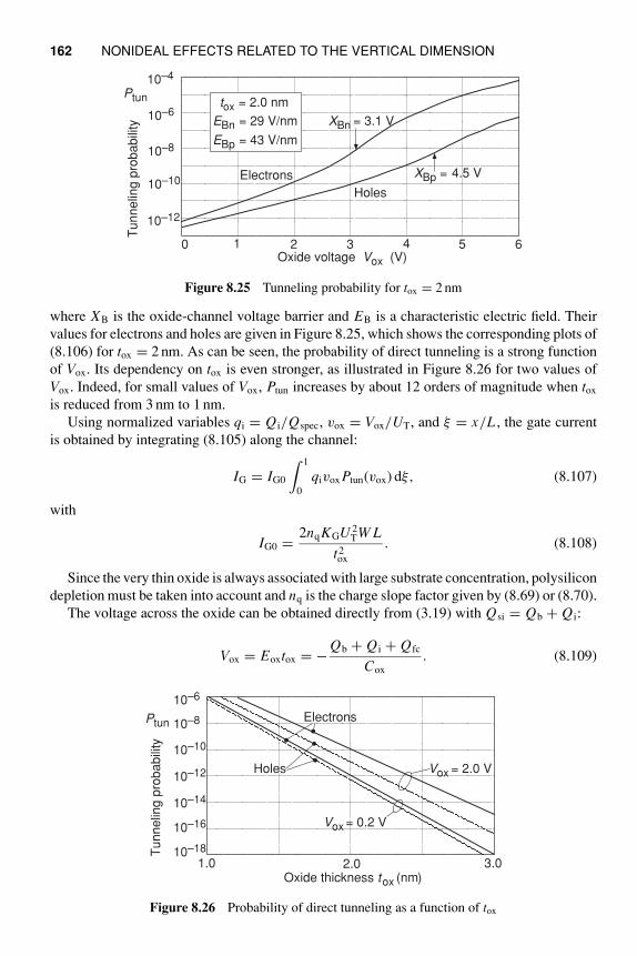
162 NONIDEAL EFFECTS RELATED TO THE VERTICAL DIMENSION
XBn = 3.1 V
XBp = 4.5 VElectrons
Holes
0 1 2 3 4 5 6
EBn = 29 V/nm
EBp = 43 V/nm
tox = 2.0 nm
10–12
10–10
10–8
10–6
10–4
Tunnelin
g p
robabili
ty
Ptun
Oxide voltage Vox (V)
Figure 8.25 Tunneling probability for tox = 2 nm
where XB is the oxide-channel voltage barrier and EB is a characteristic electric field. Their
values for electrons and holes are given in Figure 8.25, which shows the corresponding plots of
(8.106) for tox = 2 nm. As can be seen, the probability of direct tunneling is a strong function
of Vox. Its dependency on tox is even stronger, as illustrated in Figure 8.26 for two values of
Vox. Indeed, for small values of Vox, Ptun increases by about 12 orders of magnitude when tox
is reduced from 3 nm to 1 nm.
Using normalized variables qi = Qi/Qspec, vox = Vox/UT, and ξ = x/L , the gate current
is obtained by integrating (8.105) along the channel:
IG = IG0
∫ 1
0
qivox Ptun(vox) dξ, (8.107)
with
IG0 =2nq KGU 2
T W L
t2ox
. (8.108)
Since the very thin oxide is always associated with large substrate concentration, polysilicon
depletion must be taken into account and nq is the charge slope factor given by (8.69) or (8.70).
The voltage across the oxide can be obtained directly from (3.19) with Qsi = Qb + Qi:
Vox = Eoxtox = −Qb + Qi + Qfc
Cox
. (8.109)
1.0 3.02.0Oxide thickness tox (nm)
Tunnelin
g p
robabili
ty
Ptun Electrons
Holes Vox = 2.0 V
Vox = 0.2 V
10–6
10–8
10–10
10–12
10–14
10–16
10–18
Figure 8.26 Probability of direct tunneling as a function of tox
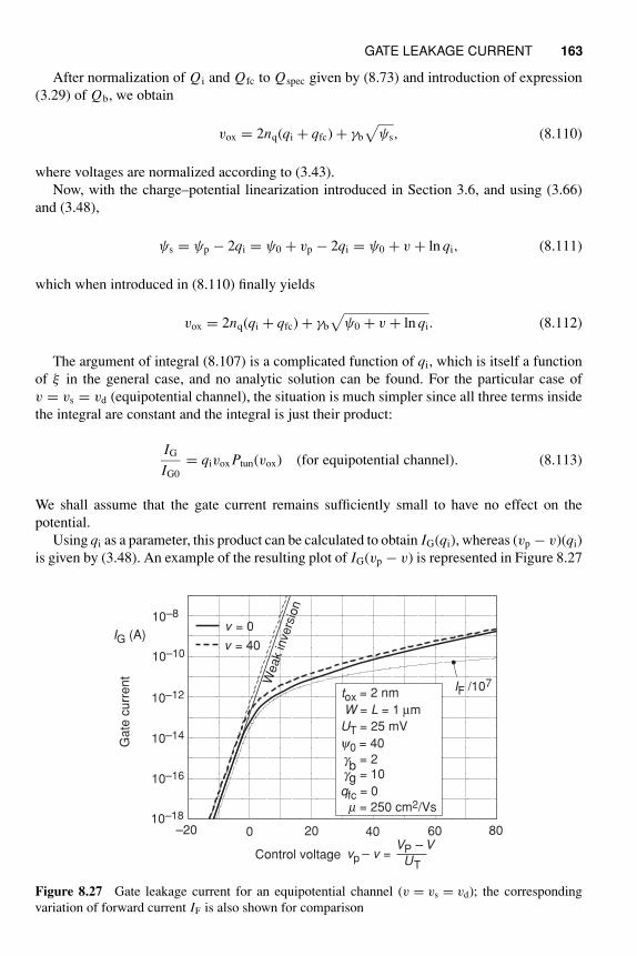
GATE LEAKAGE CURRENT 163
After normalization of Qi and Qfc to Qspec given by (8.73) and introduction of expression
(3.29) of Qb, we obtain
vox = 2nq(qi + qfc) + γb
√
ψs, (8.110)
where voltages are normalized according to (3.43).
Now, with the charge–potential linearization introduced in Section 3.6, and using (3.66)
and (3.48),
ψs = ψp − 2qi = ψ0 + vp − 2qi = ψ0 + v + ln qi, (8.111)
which when introduced in (8.110) finally yields
vox = 2nq(qi + qfc) + γb
√
ψ0 + v + ln qi. (8.112)
The argument of integral (8.107) is a complicated function of qi, which is itself a function
of ξ in the general case, and no analytic solution can be found. For the particular case of
v = vs = vd (equipotential channel), the situation is much simpler since all three terms inside
the integral are constant and the integral is just their product:
IG
IG0
= qivox Ptun(vox) (for equipotential channel). (8.113)
We shall assume that the gate current remains sufficiently small to have no effect on the
potential.
Using qi as a parameter, this product can be calculated to obtain IG(qi), whereas (vp − v)(qi)
is given by (3.48). An example of the resulting plot of IG(vp − v) is represented in Figure 8.27
0–20 20 40 60 8010–18
10–16
10–14
10–12
10–10
10–8
vp – v =VP – V
UTControl voltage
Gate
curr
ent
IG (A)v = 0
v = 40
IF /107Weak
inve
rsio
n
tox = 2 nm
W = L = 1 µm
y0 = 40
UT = 25 mV
gg = 10gb
= 2
qfc = 0
m = 250 cm2/Vs
Figure 8.27 Gate leakage current for an equipotential channel (v = vs = vd); the corresponding
variation of forward current IF is also shown for comparison
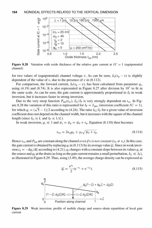
164 NONIDEAL EFFECTS RELATED TO THE VERTICAL DIMENSION
0.5 2.51.0 1.5 2.0Oxide thickness tox (nm)
IGIF
L = 1 µm
y0 = 40
UT = 25 mV
gg = 10gb
= 2
qfc = 0
Gate
curr
ent at IC
= 1
100
10--2
10--4
10--6
10--8
100 µm10 µm
m = 250 cm2/Vs
1000 µm
Figure 8.28 Variation with oxide thickness of the relative gate current at I C = 1 (equipotential
channel)
for two values of (equipotential) channel voltage v. As can be seen, IG(vp − v) is slightly
dependent of the value of v, due to the presence of v in (8.112).
For comparison, the forward current, IF(vp − v), has been calculated from parameter qi,
using (4.19) and (8.74). It is also represented in Figure 8.27 after division by 107 to fit in
the same scale. As can be seen, the gate current is approximately proportional to IF in weak
inversion, but it increases faster in strong inversion.
Due to the very steep function Ptun(tox), IG/IF is very strongly dependent on tox. In Fig-
ure 8.28 the variation of this ratio is represented for IF = Ispec (inversion coefficient I C = 1),
for which qi = (√
5 − 1)/2 according to (4.24). The ratio IG/IF for a given value of inversion
coefficient does not depend on the channel width, but it increases with the square of the channel
length (since IG ∝ L and IF ∝ 1/L).
In weak inversion, qi ≪ 1 and ψs = ψp = ψ0 + vp. Equation (8.110) then becomes
vox = 2nqqfc + γb
√
ψ0 + vp. (8.114)
Hence vox and Ptun are constant along the channel even if v is not constant (vd = vs). In this case,
the gate current is obtained by replacing qi in (8.113) by its average value qi. Since in weak inver-
sion id = −dqi/dξ according to (4.21), qi changes with a constant slope between its values qs at
the source and qd at the drain (as long as the gate current remains a small perturbation, IG ≪ IF),
as illustrated in Figure 8.29. Thus, using (3.49), the average charge density can be expressed as
qi =evp
2(e−vs + e−vd ). (8.115)
0 1x
qs
0
qd
qi
qs(1 – x) + qd x µ JG(x)
(1 – x) JG(x)dx x JG(x)dx
Position along channel
Figure 8.29 Weak inversion: profile of mobile charge and source–drain repartition of local gate
current
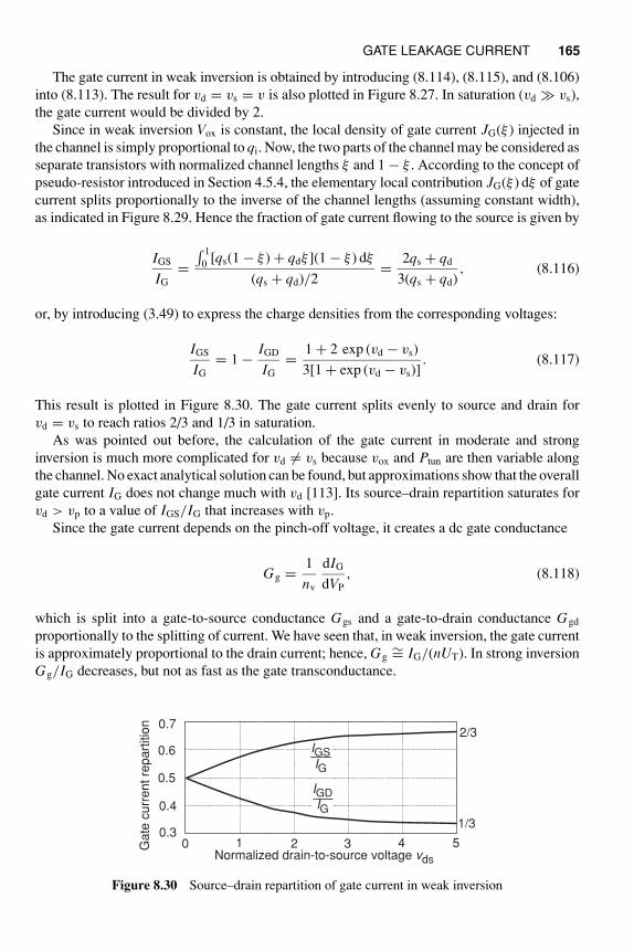
GATE LEAKAGE CURRENT 165
The gate current in weak inversion is obtained by introducing (8.114), (8.115), and (8.106)
into (8.113). The result for vd = vs = v is also plotted in Figure 8.27. In saturation (vd ≫ vs),
the gate current would be divided by 2.
Since in weak inversion Vox is constant, the local density of gate current JG(ξ ) injected in
the channel is simply proportional to qi. Now, the two parts of the channel may be considered as
separate transistors with normalized channel lengths ξ and 1 − ξ . According to the concept of
pseudo-resistor introduced in Section 4.5.4, the elementary local contribution JG(ξ ) dξ of gate
current splits proportionally to the inverse of the channel lengths (assuming constant width),
as indicated in Figure 8.29. Hence the fraction of gate current flowing to the source is given by
IGS
IG
=∫ 1
0[qs(1 − ξ ) + qdξ ](1 − ξ ) dξ
(qs + qd)/2=
2qs + qd
3(qs + qd), (8.116)
or, by introducing (3.49) to express the charge densities from the corresponding voltages:
IGS
IG
= 1 −IGD
IG
=1 + 2 exp (vd − vs)
3[1 + exp (vd − vs)]. (8.117)
This result is plotted in Figure 8.30. The gate current splits evenly to source and drain for
vd = vs to reach ratios 2/3 and 1/3 in saturation.
As was pointed out before, the calculation of the gate current in moderate and strong
inversion is much more complicated for vd = vs because vox and Ptun are then variable along
the channel. No exact analytical solution can be found, but approximations show that the overall
gate current IG does not change much with vd [113]. Its source–drain repartition saturates for
vd > vp to a value of IGS/IG that increases with vp.
Since the gate current depends on the pinch-off voltage, it creates a dc gate conductance
Gg =1
nv
dIG
dVP
, (8.118)
which is split into a gate-to-source conductance Ggs and a gate-to-drain conductance Ggd
proportionally to the splitting of current. We have seen that, in weak inversion, the gate current
is approximately proportional to the drain current; hence, Gg∼= IG/(nUT). In strong inversion
Gg/IG decreases, but not as fast as the gate transconductance.
0 1 2 3 4 50.3
0.4
0.5
0.6
0.72/3
1/3
Gate
curr
ent re
part
itio
n
Normalized drain-to-source voltage vds
IGSIG
IGDIG
Figure 8.30 Source–drain repartition of gate current in weak inversion
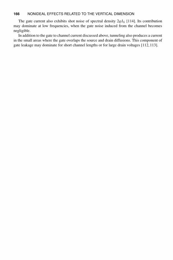
166 NONIDEAL EFFECTS RELATED TO THE VERTICAL DIMENSION
The gate current also exhibits shot noise of spectral density 2q IG [114]. Its contribution
may dominate at low frequencies, when the gate noise induced from the channel becomes
negligible.
In addition to the gate to channel current discussed above, tunneling also produces a current
in the small areas where the gate overlaps the source and drain diffusions. This component of
gate leakage may dominate for short channel lengths or for large drain voltages [112, 113].
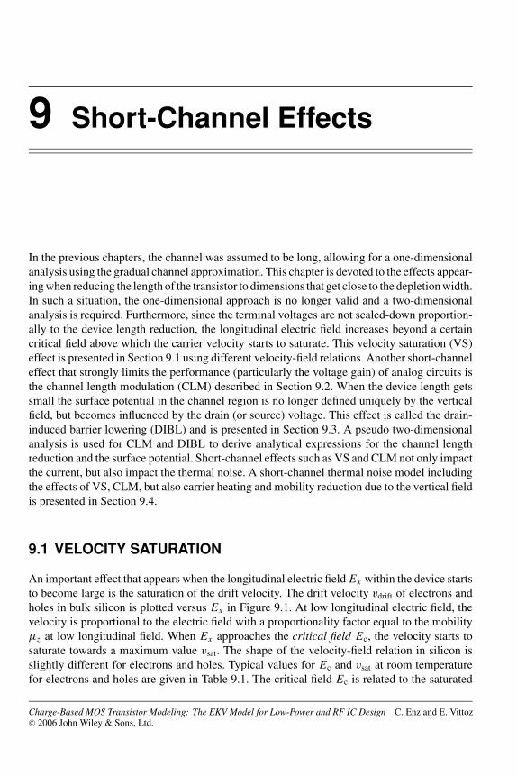
9 Short-Channel Effects
In the previous chapters, the channel was assumed to be long, allowing for a one-dimensional
analysis using the gradual channel approximation. This chapter is devoted to the effects appear-
ing when reducing the length of the transistor to dimensions that get close to the depletion width.
In such a situation, the one-dimensional approach is no longer valid and a two-dimensional
analysis is required. Furthermore, since the terminal voltages are not scaled-down proportion-
ally to the device length reduction, the longitudinal electric field increases beyond a certain
critical field above which the carrier velocity starts to saturate. This velocity saturation (VS)
effect is presented in Section 9.1 using different velocity-field relations. Another short-channel
effect that strongly limits the performance (particularly the voltage gain) of analog circuits is
the channel length modulation (CLM) described in Section 9.2. When the device length gets
small the surface potential in the channel region is no longer defined uniquely by the vertical
field, but becomes influenced by the drain (or source) voltage. This effect is called the drain-
induced barrier lowering (DIBL) and is presented in Section 9.3. A pseudo two-dimensional
analysis is used for CLM and DIBL to derive analytical expressions for the channel length
reduction and the surface potential. Short-channel effects such as VS and CLM not only impact
the current, but also impact the thermal noise. A short-channel thermal noise model including
the effects of VS, CLM, but also carrier heating and mobility reduction due to the vertical field
is presented in Section 9.4.
9.1 VELOCITY SATURATION
An important effect that appears when the longitudinal electric field Ex within the device starts
to become large is the saturation of the drift velocity. The drift velocity vdrift of electrons and
holes in bulk silicon is plotted versus Ex in Figure 9.1. At low longitudinal electric field, the
velocity is proportional to the electric field with a proportionality factor equal to the mobility
µz at low longitudinal field. When Ex approaches the critical field Ec, the velocity starts to
saturate towards a maximum value vsat. The shape of the velocity-field relation in silicon is
slightly different for electrons and holes. Typical values for Ec and vsat at room temperature
for electrons and holes are given in Table 9.1. The critical field Ec is related to the saturated
Charge-Based MOS Transistor Modeling: The EKV Model for Low-Power and RF IC Design C. Enz and E. VittozC© 2006 John Wiley & Sons, Ltd.
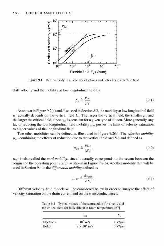
168 SHORT-CHANNEL EFFECTS
Figure 9.1 Drift velocity in silicon for electrons and holes versus electric field
drift velocity and the mobility at low longitudinal field by
Ec vsat
µz
. (9.1)
As shown in Figure 9.2(a) and discussed in Section 8.2, the mobility at low longitudinal field
µz actually depends on the vertical field Ez . The larger the vertical field, the smaller µz and
the larger the critical field, since vsat is constant for a given type of silicon. More generally, any
factor reducing the low longitudinal field mobility µz, pushes the limit of velocity saturation
to higher values of the longitudinal field.
Two other mobilities can be defined as illustrated in Figure 9.2(b). The effective mobility
µeff combining the effects of reduction due to the vertical field and VS and defined as
µeff vdrift
|Ex |. (9.2)
µeff is also called the cord mobility, since it actually corresponds to the secant between the
origin and the operating point v(Ex ), as shown in Figure 9.2(b). Another mobility that will be
used in Section 9.4 is the differential mobility defined as
µdiff dvdrift
dEx
. (9.3)
Different velocity-field models will be considered below in order to analyze the effect of
velocity saturation on the drain current and on the transconductances.
Table 9.1 Typical values of the saturated drift velocity and
the critical field for bulk silicon at room temperature [67]
vsat Ec
Electrons 105 m/s 1 V/μm
Holes 8 × 10⁴ m/s 3 V/μm
VELOCITY SATURATION 169
Figure 9.2 (a) Dependence of the mobility µz at low longitudinal field with the vertical field Ez . (b)
Illustration of the different mobilities
9.1.1 Velocity-Field Models
9.1.1.1 Model 1
The simplest model to describe the velocity-field dependence is to consider the velocity pro-
portional to the longitudinal field with a constant slope up to the critical field, above which it
stays constant and equal to the saturated velocity. This model is described by the piecewise
linear model defined by
vdrift(Ex ) =
µz|Ex | for |Ex | < Ec
vsat for |Ex | ≥ Ec,(9.4)
which can be normalized to the saturation value vsat according to
ν(e) vdrift
vsat
=
e for e < 1
1 for e ≥ 1,(9.5)
where e is the longitudinal electric field Ex normalized to the critical field Ec:
e |Ex |Ec
. (9.6)
The corresponding effective mobility μeff is then simply given by
μeff(Ex ) vdrift
|Ex |=
μz for Ex < Ec
vsat/|Ex | for Ex ≥ Ec,(9.7)
or in a normalized form
u(e) μeff
μz
=
1 for e < 1
1/e for e ≥ 1.(9.8)
170 SHORT-CHANNEL EFFECTS
The main advantage of this model is obviously its simplicity, allowing to get a first under-
standing of the physical phenomenon. But on the other hand, it has discontinuous derivatives
at e = 1 that may induce a bad behavior of the model.
9.1.1.2 Model 2
A continuous model also accounting for the difference between the velocity-field characteristics
of electrons and holes as illustrated in Figure 9.1 is defined by
vdrift(Ex ) = vsat
|Ex |/Ec
[
1 +(
|Ex |Ec
)α]1α
= μz
|Ex |[
1 +(
|Ex |Ec
)α]1α
, (9.9)
where α = 2 for electrons and α = 1 for holes. Equation (9.9) can be written in a normalized
form as
ν(e) vdrift
vsat
=e
(1 + eα)1α
. (9.10)
Note that this continuous model has been used in many compact models with the approximation
that α is equal to unity for both holes and electrons. For the sake of simplicity, we will also
make the same assumption in the following development.
The effective mobility is then given by
μeff(Ex ) vdrift
|Ex |=
μz
1 + |Ex |/Ec
, (9.11)
which can also be written in normalized form as
u(e) μeff
μz
=1
1 + e. (9.12)
9.1.1.3 Model 3
Although the continuous velocity-field model given by (9.9) and (9.10) insures the continuity
of the current and the output conductance versus the drain voltage, it requires the electric field
to become infinity at the drain for the velocity and hence the current to saturate, which is not
physical. Another velocity-field model that will also be used subsequently in Section 9.2 for
the derivation of the CLM model is given by
vdrift(Ex ) =
⎧
⎨
⎩
vsat|Ex |/Ec
1 + |Ex |/(2Ec)for |Ex | < 2Ec
vsat for |Ex | ≥ 2Ec,
(9.13)
or in normalized form
ν(e) vdrift
vsat
=
e1 + e/2
for e < 2
1 for e ≥ 2.(9.14)
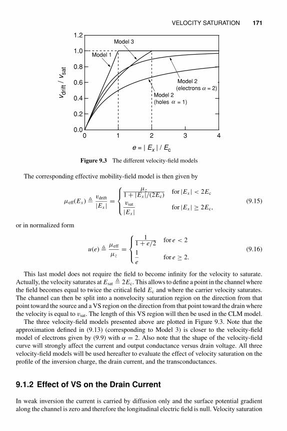
VELOCITY SATURATION 171
1.2
1.0
0.8
0.6
0.4
0.2
0.0
vd
rift / v
sa
t
43210
e = | Ex | / Ec
Model 1
Model 2
(electrons a = 2)
Model 2
(holes a = 1)
Model 3
Figure 9.3 The different velocity-field models
The corresponding effective mobility-field model is then given by
µeff(Ex ) vdrift
|Ex |=
⎧
⎪
⎨
⎪
⎩
µz
1 + |Ex |/(2Ec)for |Ex | < 2Ec
vsat
|Ex |for |Ex | ≥ 2Ec,
(9.15)
or in normalized form
u(e) µeff
µz
=
⎧
⎪
⎨
⎪
⎩
11 + e/2
for e < 2
1
efor e ≥ 2.
(9.16)
This last model does not require the field to become infinity for the velocity to saturate.
Actually, the velocity saturates at Esat 2Ec. This allows to define a point in the channel where
the field becomes equal to twice the critical field Ec and where the carrier velocity saturates.
The channel can then be split into a nonvelocity saturation region on the direction from that
point toward the source and a VS region on the direction from that point toward the drain where
the velocity is equal to vsat. The length of this VS region will then be used in the CLM model.
The three velocity-field models presented above are plotted in Figure 9.3. Note that the
approximation defined in (9.13) (corresponding to Model 3) is closer to the velocity-field
model of electrons given by (9.9) with α = 2. Also note that the shape of the velocity-field
curve will strongly affect the current and output conductance versus drain voltage. All three
velocity-field models will be used hereafter to evaluate the effect of velocity saturation on the
profile of the inversion charge, the drain current, and the transconductances.
9.1.2 Effect of VS on the Drain Current
In weak inversion the current is carried by diffusion only and the surface potential gradient
along the channel is zero and therefore the longitudinal electric field is null. Velocity saturation
172 SHORT-CHANNEL EFFECTS
Table 9.2 Typical values of the VS parameter λc
L 1 μm 0.5 μm 0.17 μm 0.1 μm
λc 0.05 0.1 0.3 0.5
can therefore be neglected in weak inversion. Although a complete model including both the
diffusion component and drift component including the effect of velocity saturation can be
derived, in the following derivation, the diffusion current is neglected for the sake of simplicity.
Note that this does not introduce a significant error in strong inversion.
The drift component of the drain current is proportional to the velocity and can be written
as
ID = W (−Qi)vdrift = W (−Qi)μeff|Ex | = W (−Qi)μeff
dΨs
dx, (9.17)
or using the normalized variables defined above
id = 2qi
ν
λc
= 2qi
ue
λc
= uqi
dψs
dξ, (9.18)
where the normalized variables id, qi, ψs, and ξ have their usual meaning. The parameter λc
accounts for the VS effect and depends on the transistor length L according to
λc 2μz UT
vsatL=
2UT
EcL. (9.19)
Note that λc tends to zero for very long-channel devices. Setting it to zero corresponds to ignore
the effect of VS. Typical values of λc for different channel lengths are given in Table 9.2.
As discussed in Section 3.6.1 and according to (3.39), the inversion charge can be linearized
with respect to Ψs giving a relation between the surface potential gradient and the inversion
charge gradient
dΨs
dx=
1
nCox
dQi
dx, (9.20)
or in normalized form
dψs
dξ= −2
dqi
dξ. (9.21)
Replacing (9.21) into (9.18) results in
id = −2uqi
dqi
dξ. (9.22)
The main difference between (9.22) and the long-channel model (4.21) (in strong inversion)
discussed in Section 4.4.1 is the field-dependent mobility term u which depends on the chosen
velocity-field model.
VELOCITY SATURATION 173
The inversion charge density at the drain −QiD (or its normalized form qd) plays a particular
role in the presence of VS. When the drift velocity saturates right at the drain, ν = 1 at ξ = 1.
The drain current cannot increase anymore and is then limited to the saturation value id sat given
by (9.18) evaluated at ξ = 1 with ν = 1 and qi = qd sat:
id sat 2
λc
qd sat, (9.23)
where qd sat is the value of the inversion charge density at the drain which is required to sustain
the drain current when carrier velocity is saturated at the drain. The main difference compared
to the long-channel situation is that the charge density at the drain does not vanish to zero as
it does at the onset of saturation for long-channel devices when vd = vp, but it has to be finite
in order for the current to flow despite the saturated velocity. To account for this saturation
of the drain charge, the normalized drain charge in strong inversion given by (3.50) has to be
modified according to
qd =
⎧
⎨
⎩
vp − vd
2for vd < vd sat
qd sat for vd ≥ vd sat,
(9.24)
where the drain saturation voltage vd sat is the value of the drain voltage at which the current
and the drain charge saturate. It is obtained by replacing qd and vd in qd = (vp − vd)/2 by qd sat
and vd sat respectively, resulting in
vd sat = vp − 2qd sat. (9.25)
Note that, due to VS, vd sat is always smaller than the pinch-off voltage vp corresponding to
the saturation voltage when velocity saturation is not present.
9.1.2.1 Model 1
In a first step, the simple piecewise linear velocity-field model given by (9.5) will be used to
derive the current. The latter is obtained by integrating (9.18) or (9.22) from source to drain,
assuming that the drain voltage is sufficiently low for the longitudinal electric field to remain
smaller than the critical field at any point along the channel. The carrier velocity is then not
saturated along the channel and hence ν = e and u = 1, resulting in
id = q2s − q2
d , (9.26)
where qs is the inversion charge density taken at the source, which in strong inversion and
assuming there is no velocity saturation at the source is related to the source voltage according
to
qs qi(ξ = 0) =vp − vs
2, (9.27)
and qd is the inversion charge density taken at the drain and given by (9.24).
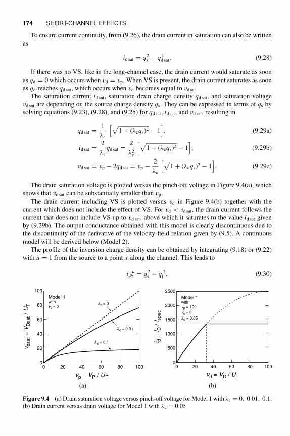
174 SHORT-CHANNEL EFFECTS
To ensure current continuity, from (9.26), the drain current in saturation can also be written
as
id sat = q2s − q2
d sat. (9.28)
If there was no VS, like in the long-channel case, the drain current would saturate as soon
as qd = 0 which occurs when vd = vp. When VS is present, the drain current saturates as soon
as qd reaches qd sat, which occurs when vd becomes equal to vd sat.
The saturation current id sat, saturation drain charge density qd sat, and saturation voltage
vd sat are depending on the source charge density qs. They can be expressed in terms of qs by
solving equations (9.23), (9.28), and (9.25) for qd sat, id sat, and vd sat, resulting in
qd sat =1
λc
[
√
1 + (λcqs)2 − 1]
, (9.29a)
id sat =2
λc
qd sat =2
λ2c
[
√
1 + (λcqs)2 − 1]
, (9.29b)
vd sat = vp − 2qd sat = vp −2
λc
[
√
1 + (λcqs)2 − 1]
. (9.29c)
The drain saturation voltage is plotted versus the pinch-off voltage in Figure 9.4(a), which
shows that vd sat can be substantially smaller than vp.
The drain current including VS is plotted versus vd in Figure 9.4(b) together with the
current which does not include the effect of VS. For vd < vd sat, the drain current follows the
current that does not include VS up to vd sat, above which it saturates to the value id sat given
by (9.29b). The output conductance obtained with this model is clearly discontinuous due to
the discontinuity of the derivative of the velocity-field relation given by (9.5). A continuous
model will be derived below (Model 2).
The profile of the inversion charge density can be obtained by integrating (9.18) or (9.22)
with u = 1 from the source to a point x along the channel. This leads to
idξ = q2s − q 2
i , (9.30)
100
80
60
40
20
0
vdsat =
VD
sa
t / U
T
100806040200
vp = VP / UT
lc = 0
lc = 0.01
lc = 0.1
Model 1withvs = 0
2500
2000
1500
1000
500
0
i d =
ID
/ I
spec
100806040200
vd = VD / UT
Model 1withvp = 100
vs = 0
lc = 0.05
(a) (b)
Figure 9.4 (a) Drain saturation voltage versus pinch-off voltage for Model 1 with λc = 0, 0.01, 0.1.
(b) Drain current versus drain voltage for Model 1 with λc = 0.05
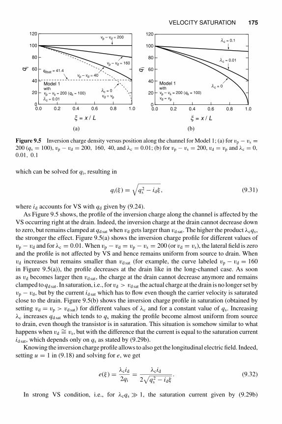
VELOCITY SATURATION 175
120
100
80
60
40
20
0
qi
1.00.80.60.40.20.0
x = x / L
Model 1withvp – vs = 200 (qs = 100)
lc = 0.01
vp – vd = 200
vp – vd = 160
vp – vd = 40qdsat = 41.4
lc = 0
vd = vp
120
100
80
60
40
20
0
qi
1.00.80.60.40.20.0
x = x / L
lc = 0
lc = 0.01
lc = 0.1
Model 1withvp – vs = 200 (qs = 100)
vd = vp
(a) (b)
Figure 9.5 Inversion charge density versus position along the channel for Model 1; (a) for vp − vs =200 (qs = 100), vp − vd = 200, 160, 40, and λc = 0.01; (b) for vp − vs = 200, vd = vp and λc = 0,
0.01, 0.1
which can be solved for qi, resulting in
qi(ξ ) =√
q2s − idξ, (9.31)
where id accounts for VS with qd given by (9.24).
As Figure 9.5 shows, the profile of the inversion charge along the channel is affected by the
VS occurring right at the drain. Indeed, the inversion charge at the drain cannot decrease down
to zero, but remains clamped at qd sat when vd gets larger than vd sat. The higher the product λcqs,
the stronger the effect. Figure 9.5(a) shows the inversion charge profile for different values of
vp − vd and for λc = 0.01. When vp − vd = vp − vs = 200 (or vd = vs), the lateral field is zero
and the profile is not affected by VS and hence remains uniform from source to drain. When
vd increases but remains smaller than vd sat (for example, the curve labeled vp − vd = 160
in Figure 9.5(a)), the profile decreases at the drain like in the long-channel case. As soon
as vd becomes larger then vd sat, the charge at the drain cannot decrease anymore and remains
clamped to qd sat. In saturation, i.e., for vd > vd sat the actual charge at the drain is no longer set by
vp − vd, but by the current id sat which has to flow even though the carrier velocity is saturated
close to the drain. Figure 9.5(b) shows the inversion charge profile in saturation (obtained by
setting vd = vp > vd sat) for different values of λc and for a constant value of qs. Increasing
λc increases qd sat which tends to qs making the profile become almost uniform from source
to drain, even though the transistor is in saturation. This situation is somehow similar to what
happens when vd∼= vs, but with the difference that the current is equal to the saturation current
id sat, which depends only on qs as stated by (9.29b).
Knowing the inversion charge profile allows to also get the longitudinal electric field. Indeed,
setting u = 1 in (9.18) and solving for e, we get
e(ξ ) =λcid
2qi
=λcid
2√
q2s − idξ
. (9.32)
In strong VS condition, i.e., for λcqs ≫ 1, the saturation current given by (9.29b)
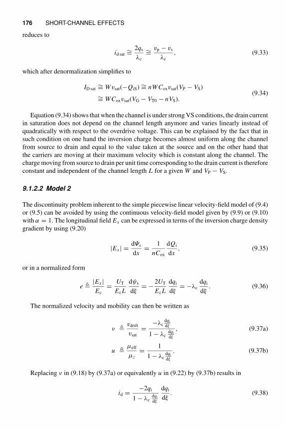
176 SHORT-CHANNEL EFFECTS
reduces to
id sat∼=
2qs
λc
∼=vp − vs
λc
, (9.33)
which after denormalization simplifies to
ID sat∼= Wvsat(−QiS) ∼= nWCoxvsat(VP − VS)
∼= WCoxvsat(VG − VT0 − nVS).(9.34)
Equation (9.34) shows that when the channel is under strong VS conditions, the drain current
in saturation does not depend on the channel length anymore and varies linearly instead of
quadratically with respect to the overdrive voltage. This can be explained by the fact that in
such condition on one hand the inversion charge becomes almost uniform along the channel
from source to drain and equal to the value taken at the source and on the other hand that
the carriers are moving at their maximum velocity which is constant along the channel. The
charge moving from source to drain per unit time corresponding to the drain current is therefore
constant and independent of the channel length L for a given W and VP − VS.
9.1.2.2 Model 2
The discontinuity problem inherent to the simple piecewise linear velocity-field model of (9.4)
or (9.5) can be avoided by using the continuous velocity-field model given by (9.9) or (9.10)
with α = 1. The longitudinal field Ex can be expressed in terms of the inversion charge density
gradient by using (9.20)
|Ex | =dΨs
dx=
1
nCox
dQi
dx, (9.35)
or in a normalized form
e |Ex |Ec
=UT
EcL
dψs
dξ= −
2UT
EcL
dqi
dξ= −λc
dqi
dξ. (9.36)
The normalized velocity and mobility can then be written as
ν vdrift
vsat
=−λc
dqi
dξ
1 − λcdqi
dξ
, (9.37a)
u μeff
μz
=1
1 − λcdqi
dξ
. (9.37b)
Replacing ν in (9.18) by (9.37a) or equivalently u in (9.22) by (9.37b) results in
id =−2qi
1 − λcdqi
dξ
dqi
dξ. (9.38)
VELOCITY SATURATION 177
Rearranging (9.38) leads to
id = − (2qi − λcid)dqi
dξ. (9.39)
Integrating (9.39) from source (where ξ = 0 and qi = qs) to drain (where ξ = 1 and qi = qd)
leads to
id = −∫ qd
qs
(2qi − λcid) dqi
=∫ qs
qd
2qidqi − λcid
∫ qs
qd
dqi (9.40)
= q2s − q2
d − λcid(qs − qd).
Solving (9.40) for id results in the current expression accounting for VS using the continuous
velocity-field model (Model 2):
id =q2
s − q2d
1 + λc(qs − qd). (9.41)
The drain current given by (9.41) is plotted in Figure 9.6(b) and compared to the current with-
out any VS effect. Note that the drain charge density qd in (9.41) should be taken equal to (9.24)
to account for the saturation of qd to qd sat when vd ≥ vd sat. If qd is taken equal to (vp − vd)/2
instead (without accounting for the saturation), the current reaches a maximum at vd = vd sat
and then decreases as shown by the dashed line in Figure 9.6(b). Now, the current cannot actu-
ally decrease, but must saturate to id sat for vd ≥ vd sat. The charge at the drain must also saturate
to qd = qd sat for vd ≥ vd sat. Also note that at the onset of saturation, the electric field right at
the drain has to tend to infinity in order for the velocity to tend to the saturation velocity vsat.
The saturation current is obtained by replacing id and qd in (9.41) by id sat and qd sat, respec-
tively, resulting in
id sat =q2
s − q2d sat
1 + λc(qs − qd sat). (9.42)
100
80
60
40
20
0
vd
sa
t =
VD
sat / U
T
100806040200
vp = VP / UT
lc = 0
lc = 0.01
lc = 0.1
Model 2withvs = 0
2500
2000
1500
1000
500
0
i d =
ID
/ I
sp
ec
100806040200
vd = VD / UT
Model 2withvp = 100
vs = 0
lc = 0.05
(a) (b)
Figure 9.6 (a) Drain saturation voltage versus pinch-off voltage for Model 2 with λc = 0, 0.01, 0.1.
(b) Drain current versus drain voltage for Model 2 with λc = 0.05
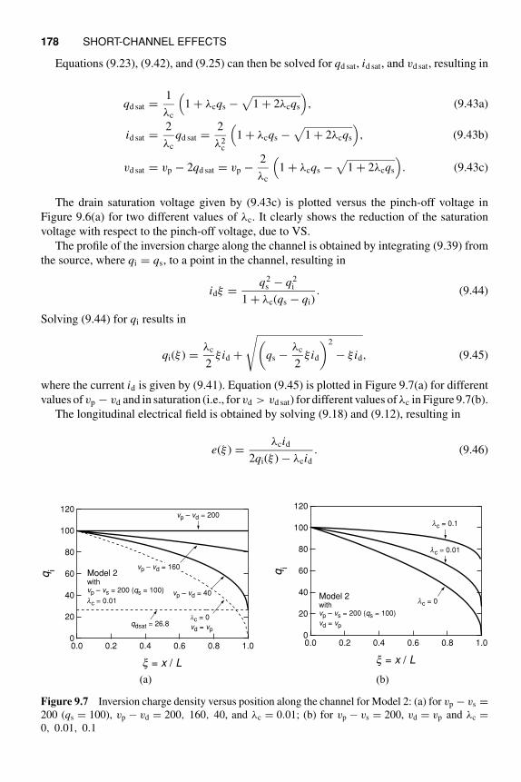
178 SHORT-CHANNEL EFFECTS
Equations (9.23), (9.42), and (9.25) can then be solved for qd sat, id sat, and vd sat, resulting in
qd sat =1
λc
(
1 + λcqs −√
1 + 2λcqs
)
, (9.43a)
id sat =2
λc
qd sat =2
λ2c
(
1 + λcqs −√
1 + 2λcqs
)
, (9.43b)
vd sat = vp − 2qd sat = vp −2
λc
(
1 + λcqs −√
1 + 2λcqs
)
. (9.43c)
The drain saturation voltage given by (9.43c) is plotted versus the pinch-off voltage in
Figure 9.6(a) for two different values of λc. It clearly shows the reduction of the saturation
voltage with respect to the pinch-off voltage, due to VS.
The profile of the inversion charge along the channel is obtained by integrating (9.39) from
the source, where qi = qs, to a point in the channel, resulting in
idξ =q2
s − q2i
1 + λc(qs − qi). (9.44)
Solving (9.44) for qi results in
qi(ξ ) =λc
2ξ id +
√
(
qs −λc
2ξ id
)2
− ξ id, (9.45)
where the current id is given by (9.41). Equation (9.45) is plotted in Figure 9.7(a) for different
values of vp − vd and in saturation (i.e., for vd > vd sat) for different values of λc in Figure 9.7(b).
The longitudinal electrical field is obtained by solving (9.18) and (9.12), resulting in
e(ξ ) =λcid
2qi(ξ ) − λcid
. (9.46)
120
100
80
60
40
20
0
qi
1.00.80.60.40.20.0
x = x / L
Model 2withvp – vs = 200 (qs = 100)
lc = 0.01vp – vd = 40
vp – vd = 160
vp – vd = 200
qdsat = 26.8lc = 0
vd = vp
120
100
80
60
40
20
01.00.80.60.40.20.0
x = x / L
lc = 0
lc = 0.01
lc = 0.1
Model 2withvp – vs = 200 (qs = 100)
vd = vp
qi
(a) (b)
Figure 9.7 Inversion charge density versus position along the channel for Model 2: (a) for vp − vs =200 (qs = 100), vp − vd = 200, 160, 40, and λc = 0.01; (b) for vp − vs = 200, vd = vp and λc =0, 0.01, 0.1
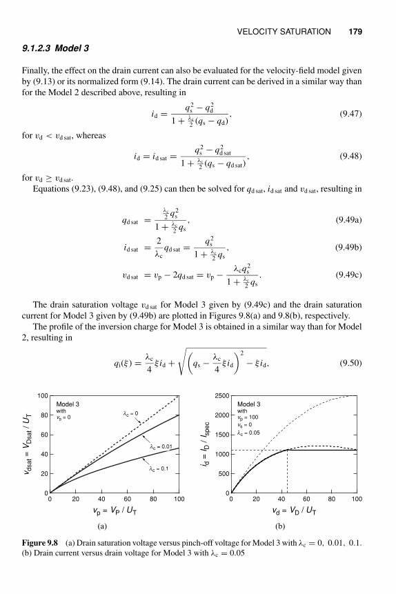
VELOCITY SATURATION 179
9.1.2.3 Model 3
Finally, the effect on the drain current can also be evaluated for the velocity-field model given
by (9.13) or its normalized form (9.14). The drain current can be derived in a similar way than
for the Model 2 described above, resulting in
id =q2
s − q2d
1 + λc
2(qs − qd)
, (9.47)
for vd < vd sat, whereas
id = id sat =q2
s − q2d sat
1 + λc
2(qs − qd sat)
, (9.48)
for vd ≥ vd sat.
Equations (9.23), (9.48), and (9.25) can then be solved for qd sat, id sat and vd sat, resulting in
qd sat =λc
2q2
s
1 + λc
2qs
, (9.49a)
id sat =2
λc
qd sat =q2
s
1 + λc
2qs
, (9.49b)
vd sat = vp − 2qd sat = vp −λcq
2s
1 + λc
2qs
. (9.49c)
The drain saturation voltage vd sat for Model 3 given by (9.49c) and the drain saturation
current for Model 3 given by (9.49b) are plotted in Figures 9.8(a) and 9.8(b), respectively.
The profile of the inversion charge for Model 3 is obtained in a similar way than for Model
2, resulting in
qi(ξ ) =λc
4ξ id +
√
(
qs −λc
4ξ id
)2
− ξ id, (9.50)
100
80
60
40
20
0
vd
sa
t =
VD
sa
t / U
T
100806040200
vp = VP / UT
lc = 0
lc = 0.01
lc = 0.1
Model 3withvs = 0
2500
2000
1500
1000
500
0
i d =
ID
/ I
spec
100806040200
vd = VD / UT
Model 3withvp = 100
vs = 0
lc = 0.05
(a) (b)
Figure 9.8 (a) Drain saturation voltage versus pinch-off voltage for Model 3 with λc = 0, 0.01, 0.1.
(b) Drain current versus drain voltage for Model 3 with λc = 0.05
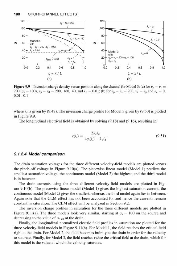
180 SHORT-CHANNEL EFFECTS
120
100
80
60
40
20
0
qi
1.00.80.60.40.20.0
x = x / L
Model 3withvp – vs = 200 (qs = 100)
λc = 0.01
vp – vd = 200
vp – vd = 160
vp – vd = 40
qdsat = 33.3 lc = 0
vd = vp
120
100
80
60
40
20
0
qi
1.00.80.60.40.20.0
x = x / L
lc = 0
lc = 0.01
lc = 0.1
Model 3withvp – vs = 200 (qs = 100)
vd = vp
(a) (b)
Figure 9.9 Inversion charge density versus position along the channel for Model 3: (a) for vp − vs =200 (qs = 100), vp − vd = 200, 160, 40, and λc = 0.01; (b) for vp − vs = 200, vd = vp and λc = 0,
0.01, 0.1
where id is given by (9.47). The inversion charge profile for Model 3 given by (9.50) is plotted
in Figure 9.9.
The longitudinal electrical field is obtained by solving (9.18) and (9.16), resulting in
e(ξ ) =2λcid
4qi(ξ ) − λcid
. (9.51)
9.1.2.4 Model comparison
The drain saturation voltages for the three different velocity-field models are plotted versus
the pinch-off voltage in Figure 9.10(a). The piecewise linear model (Model 1) predicts the
smallest saturation voltage, the continuous model (Model 2) the highest, and the third model
is in between.
The drain currents using the three different velocity-field models are plotted in Fig-
ure 9.10(b). The piecewise linear model (Model 1) gives the highest saturation current, the
continuous model (Model 2) gives the smallest, whereas the third model again lies in between.
Again note that the CLM effect has not been accounted for and hence the currents remain
constant in saturation. The CLM effect will be analyzed in Section 9.2.
The inversion charge profiles in saturation for the three different models are plotted in
Figure 9.11(a). The three models look very similar, starting at qs = 100 on the source and
decreasing to the value of qd sat at the drain.
Finally, the longitudinal normalized electric field profiles in saturation are plotted for the
three velocity-field models in Figure 9.11(b). For Model 1, the field reaches the critical field
right at the drain. For Model 2, the field becomes infinity at the drain in order for the velocity
to saturate. Finally, for Model 3, the field reaches twice the critical field at the drain, which for
this model is the value at which the velocity saturates.
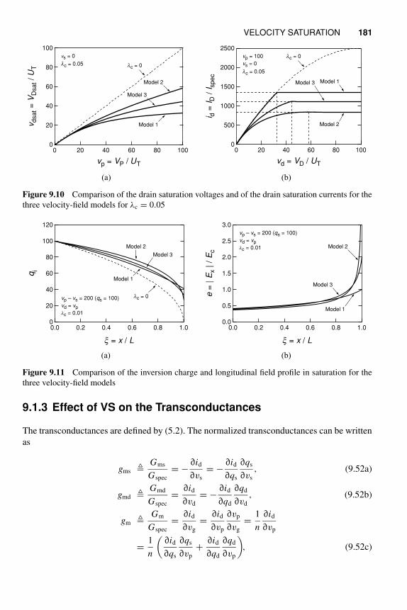
VELOCITY SATURATION 181
100
80
60
40
20
0
vdsat =
VD
sat / U
T
100806040200
vp = VP / UT
lc = 0
vs = 0
lc = 0.05
Model 2
Model 1
Model 3
2500
2000
1500
1000
500
0
i d =
ID
/ I
sp
ec
100806040200
vd = VD / UT
vp = 100
vs = 0
lc = 0.05
Model 1
Model 2
Model 3
lc = 0
(a) (b)
Figure 9.10 Comparison of the drain saturation voltages and of the drain saturation currents for the
three velocity-field models for λc = 0.05
120
100
80
60
40
20
0
qi
1.00.80.60.40.20.0
x = x / L
lc = 0vp – vs = 200 (qs = 100)
vd = vp
lc = 0.01
Model 1
Model 3
Model 2
3.0
2.5
2.0
1.5
1.0
0.5
0.0
e =
| E
x | / E
c
1.00.80.60.40.20.0
x = x / L
Model 1
Model 2
Model 3
vp – vs = 200 (qs = 100)
vd = vp
lc = 0.01
(a) (b)
Figure 9.11 Comparison of the inversion charge and longitudinal field profile in saturation for the
three velocity-field models
9.1.3 Effect of VS on the Transconductances
The transconductances are defined by (5.2). The normalized transconductances can be written
as
gms Gms
Gspec
= −∂id
∂vs
= −∂id
∂qs
∂qs
∂vs
, (9.52a)
gmd Gmd
Gspec
=∂id
∂vd
= −∂id
∂qd
∂qd
∂vd
, (9.52b)
gm Gm
Gspec
=∂id
∂vg
=∂id
∂vp
∂vp
∂vg
=1
n
∂id
∂vp
=1
n
(
∂id
∂qs
∂qs
∂vp
+∂id
∂qd
∂qd
∂vp
)
, (9.52c)
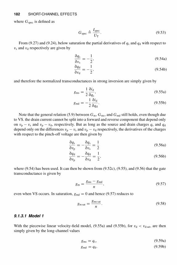
182 SHORT-CHANNEL EFFECTS
where Gspec is defined as
Gspec Ispec
UT
. (9.53)
From (9.27) and (9.24), below saturation the partial derivatives of qs and qd with respect to
vs and vd respectively are given by
∂qs
∂vs
= −1
2, (9.54a)
∂qd
∂vd
= −1
2, (9.54b)
and therefore the normalized transconductances in strong inversion are simply given by
gms =1
2
∂id
∂qs
, (9.55a)
gmd = −1
2
∂id
∂qd
. (9.55b)
Note that the general relation (5.9) between Gm, Gms, and Gmd still holds, even though due
to VS. the drain current cannot be split into a forward and reverse component that depend only
on vp − vs and vp − vd, respectively. But as long as the source and drain charges qs and qd
depend only on the differences vp − vs and vp − vd respectively, the derivatives of the charges
with respect to the pinch-off voltage are then given by
∂qs
∂vp
= −∂qs
∂vs
=1
2(9.56a)
∂qd
∂vp
= −∂qd
∂vd
=1
2, (9.56b)
where (9.54) has been used. It can then be shown from (9.52c), (9.55), and (9.56) that the gate
transconductance is given by
gm =gms − gmd
n, (9.57)
even when VS occurs. In saturation, gmd = 0 and hence (9.57) reduces to
gm sat =gms sat
n. (9.58)
9.1.3.1 Model 1
With the piecewise linear velocity-field model, (9.55a) and (9.55b), for vd < vd sat, are then
simply given by the long-channel values
gms = qs, (9.59a)
gmd = qd. (9.59b)
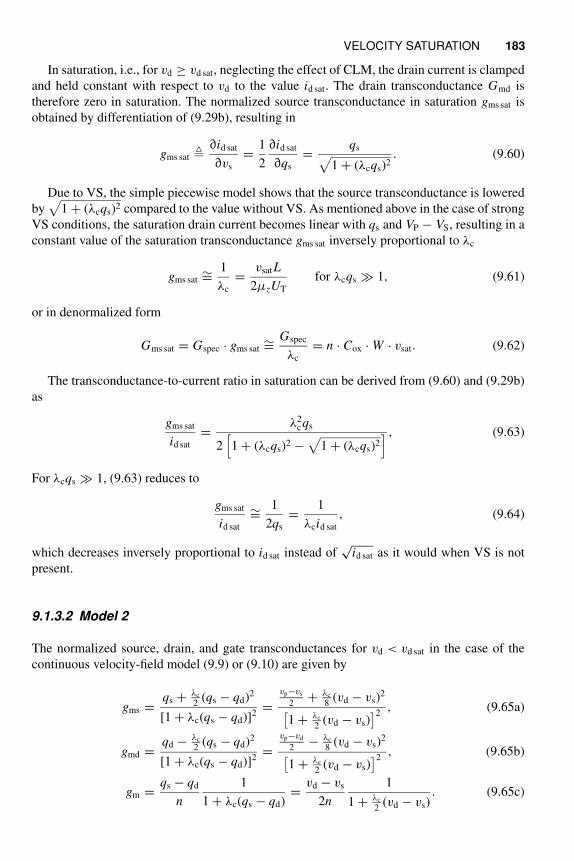
VELOCITY SATURATION 183
In saturation, i.e., for vd ≥ vd sat, neglecting the effect of CLM, the drain current is clamped
and held constant with respect to vd to the value id sat. The drain transconductance Gmd is
therefore zero in saturation. The normalized source transconductance in saturation gms sat is
obtained by differentiation of (9.29b), resulting in
gms sat ∂id sat
∂vs
=1
2
∂id sat
∂qs
=qs
√
1 + (λcqs)2. (9.60)
Due to VS, the simple piecewise model shows that the source transconductance is lowered
by√
1 + (λcqs)2 compared to the value without VS. As mentioned above in the case of strong
VS conditions, the saturation drain current becomes linear with qs and VP − VS, resulting in a
constant value of the saturation transconductance gms sat inversely proportional to λc
gms sat∼=
1
λc
=vsatL
2μzUT
for λcqs ≫ 1, (9.61)
or in denormalized form
Gms sat = Gspec · gms sat∼=
Gspec
λc
= n · Cox · W · vsat. (9.62)
The transconductance-to-current ratio in saturation can be derived from (9.60) and (9.29b)
as
gms sat
id sat
=λ2
cqs
2[
1 + (λcqs)2 −√
1 + (λcqs)2
] , (9.63)
For λcqs ≫ 1, (9.63) reduces to
gms sat
id sat
∼=1
2qs
=1
λcid sat
, (9.64)
which decreases inversely proportional to id sat instead of√
id sat as it would when VS is not
present.
9.1.3.2 Model 2
The normalized source, drain, and gate transconductances for vd < vd sat in the case of the
continuous velocity-field model (9.9) or (9.10) are given by
gms =qs + λc
2(qs − qd)2
[1 + λc(qs − qd)]2=
vp−vs
2+ λc
8(vd − vs)
2
[
1 + λc
2(vd − vs)
]2, (9.65a)
gmd =qd − λc
2(qs − qd)2
[1 + λc(qs − qd)]2=
vp−vd
2− λc
8(vd − vs)
2
[
1 + λc
2(vd − vs)
]2, (9.65b)
gm =qs − qd
n
1
1 + λc(qs − qd)=
vd − vs
2n
1
1 + λc
2(vd − vs)
. (9.65c)
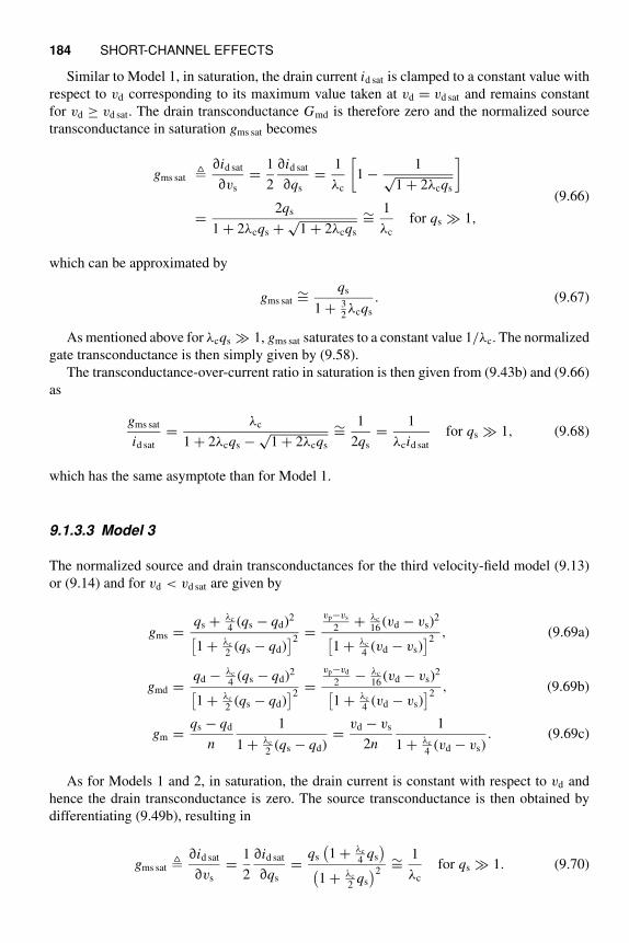
184 SHORT-CHANNEL EFFECTS
Similar to Model 1, in saturation, the drain current id sat is clamped to a constant value with
respect to vd corresponding to its maximum value taken at vd = vd sat and remains constant
for vd ≥ vd sat. The drain transconductance Gmd is therefore zero and the normalized source
transconductance in saturation gms sat becomes
gms sat ∂id sat
∂vs
=1
2
∂id sat
∂qs
=1
λc
[
1 −1
√1 + 2λcqs
]
=2qs
1 + 2λcqs +√
1 + 2λcqs
∼=1
λc
for qs ≫ 1,
(9.66)
which can be approximated by
gms sat∼=
qs
1 + 32λcqs
. (9.67)
As mentioned above for λcqs ≫ 1, gms sat saturates to a constant value 1/λc. The normalized
gate transconductance is then simply given by (9.58).
The transconductance-over-current ratio in saturation is then given from (9.43b) and (9.66)
as
gms sat
id sat
=λc
1 + 2λcqs −√
1 + 2λcqs
∼=1
2qs
=1
λcid sat
for qs ≫ 1, (9.68)
which has the same asymptote than for Model 1.
9.1.3.3 Model 3
The normalized source and drain transconductances for the third velocity-field model (9.13)
or (9.14) and for vd < vd sat are given by
gms =qs + λc
4(qs − qd)2
[
1 + λc
2(qs − qd)
]2=
vp−vs
2+ λc
16(vd − vs)
2
[
1 + λc
4(vd − vs)
]2, (9.69a)
gmd =qd − λc
4(qs − qd)2
[
1 + λc
2(qs − qd)
]2=
vp−vd
2− λc
16(vd − vs)
2
[
1 + λc
4(vd − vs)
]2, (9.69b)
gm =qs − qd
n
1
1 + λc
2(qs − qd)
=vd − vs
2n
1
1 + λc
4(vd − vs)
. (9.69c)
As for Models 1 and 2, in saturation, the drain current is constant with respect to vd and
hence the drain transconductance is zero. The source transconductance is then obtained by
differentiating (9.49b), resulting in
gms sat ∂id sat
∂vs
=1
2
∂id sat
∂qs
=qs
(
1 + λc
4qs
)
(
1 + λc
2qs
)2∼=
1
λc
for qs ≫ 1. (9.70)
VELOCITY SATURATION 185
The transconductance-over-current ratio in saturation is then given from (9.49b) and (9.70)
as
gms sat
id sat
=1 + λc
4qs
qs
(1 + λc
2qs
) ∼=1
2qs
=1
λcid sat
for qs ≫ 1. (9.71)
9.1.3.4 Model comparison
The normalized source transconductances in saturation for the three models are plotted versus
the normalized pinch-off voltage in Figure 9.12(a) for λc = 0.1. As mentioned at the end of
Section 9.1.2.1, the drain current in saturation becomes linear instead of quadratic with respect
to the overdrive voltage VP − VS (c.f. equation (9.34) and hence the source transconductance
in saturation saturates to a constant value equal to 1/λc as soon as velocity saturates.
The degradation of the source transconductance due to VS can be evaluated by defining the
ratio of the source transconductance in saturation to the source transconductance in saturation
without the effect of VS (which actually is simply equal to qs)
χms sat gms sat
gms sat|λc=0
=gms sat
qs
. (9.72)
For the first piecewise linear model (Model 1), the degradation is given by
χms sat =1
√
1 + (λcqs)2, (9.73)
whereas for the continuous model (Model 2), it is given by
χms sat =2
1 + 2λcqs +√
1 + 2λcqs
∼=1
1 + 32λcqs
∼=1
1 + 34λc(vp − vs)
.
(9.74)
10
8
6
4
2
0
gm
ssa
t =
Gm
ssa
t /
Gsp
ec
100806040200
vp = VP / UT
Model 1
vs = 0
lc = 0.1
Model 2
Model 3
1.0
0.8
0.6
0.4
0.2
0.0
cm
ssa
t =
gm
ssa
t / q
s
100806040200
vp = VP / UT
Model 1
vs = 0
lc = 0.1
Model 2
Model 3
(a) (b)
Figure 9.12 (a) Source transconductance and (b) source transconductance degradation versus the
pinch-off voltage for the three velocity-field models
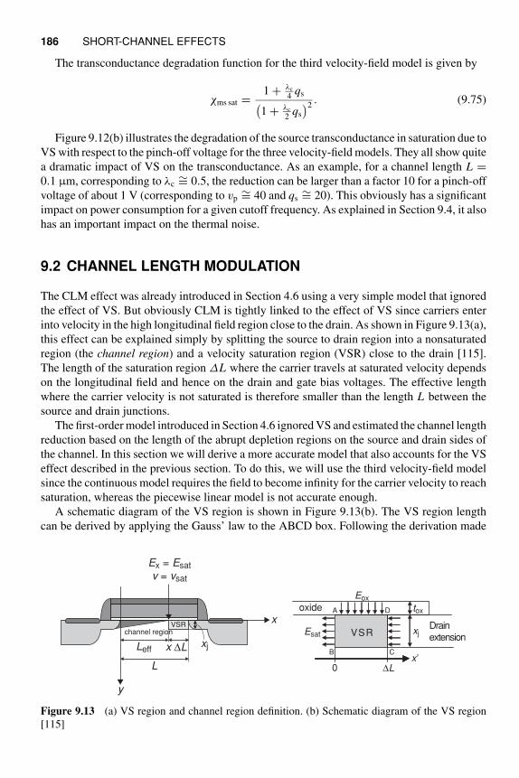
186 SHORT-CHANNEL EFFECTS
The transconductance degradation function for the third velocity-field model is given by
χms sat =1 + λc
4qs
(1 + λc
2qs
)2. (9.75)
Figure 9.12(b) illustrates the degradation of the source transconductance in saturation due to
VS with respect to the pinch-off voltage for the three velocity-field models. They all show quite
a dramatic impact of VS on the transconductance. As an example, for a channel length L =0.1 μm, corresponding to λc
∼= 0.5, the reduction can be larger than a factor 10 for a pinch-off
voltage of about 1 V (corresponding to vp∼= 40 and qs
∼= 20). This obviously has a significant
impact on power consumption for a given cutoff frequency. As explained in Section 9.4, it also
has an important impact on the thermal noise.
9.2 CHANNEL LENGTH MODULATION
The CLM effect was already introduced in Section 4.6 using a very simple model that ignored
the effect of VS. But obviously CLM is tightly linked to the effect of VS since carriers enter
into velocity in the high longitudinal field region close to the drain. As shown in Figure 9.13(a),
this effect can be explained simply by splitting the source to drain region into a nonsaturated
region (the channel region) and a velocity saturation region (VSR) close to the drain [115].
The length of the saturation region ΔL where the carrier travels at saturated velocity depends
on the longitudinal field and hence on the drain and gate bias voltages. The effective length
where the carrier velocity is not saturated is therefore smaller than the length L between the
source and drain junctions.
The first-order model introduced in Section 4.6 ignored VS and estimated the channel length
reduction based on the length of the abrupt depletion regions on the source and drain sides of
the channel. In this section we will derive a more accurate model that also accounts for the VS
effect described in the previous section. To do this, we will use the third velocity-field model
since the continuous model requires the field to become infinity for the carrier velocity to reach
saturation, whereas the piecewise linear model is not accurate enough.
A schematic diagram of the VS region is shown in Figure 9.13(b). The VS region length
can be derived by applying the Gauss’ law to the ABCD box. Following the derivation made
L
Leff
x
x ∆L
VSRchannel region
y
Ex = Esat
v = vsat
xj
Drainextension
oxide
x’0
Esat
Eox
A
B C
D
VSR
∆L
tox
xj
Figure 9.13 (a) VS region and channel region definition. (b) Schematic diagram of the VS region
[115]
CHANNEL LENGTH MODULATION 187
in [115], we will assume that (a) the carriers in the VS region are traveling with a saturated
velocity; (b) the junction on the drain extension region is abrupt and the drain extension is
heavily doped and hence is perfectly conducting; and (c) the current flows no deeper than
the junction depth and is confined in the box. To simplify the derivation, we also change the
coordinate system as indicated in Figure 9.13(b). To apply Gauss’ law, we will further assume
that the field is independent of y and that the field lines crossing the BC boundary contribute
very little. This results in
−ǫsixjW Esat + ǫsixjW Ex(x ′) + ǫoxW
∫ x ′
0
Eox(x ′) dx ′ = QboxW x ′, (9.76)
where Eox(x ′) is simply given by
Eox(x ′) =VG − VFB − Ψ0 − V (x ′)
tox
, (9.77)
and Qbox qnpxj + q Nbxj corresponds to the charge per unit area in the VSR with np being
the electron concentration and Nb the fixed charge concentration.
Since the current and velocity are constant in the VSR, np is also constant in the VSR and
hence differentiating (9.76) with respect to x ′ results in
ǫsixj
dEx (x ′)
dx ′+ ǫox Eox(x ′) = Qbox. (9.78)
Replacing Eox in (9.78) by (9.77) results in
ǫsixj
dEx (x ′)
dx ′+ Cox[VG − VFB − Ψ0 − V (x ′)] = Qbox. (9.79)
On the left side of the VS region, the gradual channel approximation applies and the gradient
of the longitudinal field can be ignored compared to the gradient of the vertical field. That is, in
this region, all the silicon charges are controlled by the vertical field only. This approximation
also applies to the boundary at x ′ = 0, where the channel voltage V (x ′ = 0) is equal to the
saturation voltage VD sat. The gradient of the longitudinal field dEx (x ′)/dx ′ in (9.79) can hence
be neglected and (9.79) then simplifies to
ǫox Eox(x ′ = 0) = Cox (VG − VFB − Ψ0 − VD sat) = Qbox. (9.80)
The saturation voltage VD sat normalized to UT is given by (9.49c). Replacing Qbox in (9.79)
by (9.80) results in
dEx (x ′)
dx ′=
V (x ′) − VD sat
ℓ2, (9.81)
where
ℓ
√
ǫsi
ǫox
toxxj =
√
ǫsixj
Cox
. (9.82)
188 SHORT-CHANNEL EFFECTS
Differential equation (9.81) can be solved by applying the boundary conditions E(x ′ = 0) =
Esat = 2Ec and V (x ′ = 0) = VD sat, resulting in
Ex (x ′) = Esat cosh
(
x ′
ℓ
)
(9.83)
and
V (x ′) = VD sat + ℓEsat sinh
(
x ′
ℓ
)
. (9.84)
Equation (9.83) indicates that the field increases almost exponentially close to the drain
where it becomes maximum at the end of the VS region and is given by
Ex (x ′ = ΔL) = Emax = Esat cosh
(
ΔL
ℓ
)
, (9.85)
whereas
V (x ′ = ΔL) = VD = VD sat + ℓEsat sinh
(
ΔL
ℓ
)
. (9.86)
Equations (9.85) and (9.86) can then be solved for ΔL and Emax
ΔL = ℓ asinh(u) = ℓ ln(
u +√
u2 + 1)
, (9.87a)
Emax = Esat
√
u2 + 1, (9.87b)
where
u VD − VD sat
ℓEsat
. (9.88)
The channel length reduction normalized to ℓ is plotted versus u in Figure 9.14.
3.0
2.5
2.0
1.5
1.0
0.5
0.0
∆L/l
1086420
u = (VD – VDsat)/(l·Esat )
Figure 9.14 Channel length reduction ΔL/ℓ versus u (VD − VD sat)/(ℓEsat)
DRAIN INDUCED BARRIER LOWERING 189
--Eox
Ex + dEx
Ey = 0
Ez = 0
QsidxEx
x
z
td
0
1
Qfc dx,Ys
dx
y
Depletion depth
Unit width
L
Figure 9.15 Application of Gauss’ law to calculate Qsi
9.3 DRAIN INDUCED BARRIER LOWERING
9.3.1 Introduction
With the gradual channel approximation used to develop the long-channel model in Part I, the
second derivative of the channel potential (first derivative of the electric field) was assumed to
be negligible along the channel. As a consequence, the charge density in silicon Qsi depended
only on the vertical surface field as illustrated in Figure 3.2. This approximation is no longer
acceptable for short-channel transistors, and the variation of the horizontal field Ex must
be included in the calculation of Qsi, as illustrated in Figure 9.15. This figure depicts an
elementary volume of unit width and of length dx . Its depth is td, the depletion depth (or
depletion thickness), beyond which the potential is assumed to be constant (Ψ = 0).
The negative elementary charge Qsi dx enclosed in this volume is increased in absolute value
by the difference dEx <0 of the horizontal field created by the drain voltage. Alternately, the
value of Eox needed to obtain a given charge density is reduced, corresponding to an increase of
surface potential. Hence the name drain induced barrier lowering (DIBL) given to this effect.
9.3.2 Evaluation of the Surface Potential
Following the analysis carried out in [116], the application of Gauss’ law to the elementary
volume depicted in Figure 9.15 results in
(Qsi + Qfc) dx = −ǫox Eox dx + ǫsitd dEx , (9.89)
where dEx is assumed to be constant across the depletion depth td, with
dEx
dx= −
d2Ψs
dx2< 0. (9.90)
By introducing expression (2.3) of Eox and definition (3.22) of VFB, we obtain a second-order
differential equation of Ψs:
−L2c
d2Ψs
dx2+ Ψs = VG − VFB +
Qsi
Cox
, (9.91)
190 SHORT-CHANNEL EFFECTS
where Lc is a characteristic length defined by
Lc
√ǫsitd
Cox
. (9.92)
Now, td is itself slightly dependent on the surface potential Ψs; hence, equation (9.91) is
nonlinear. This dependency is weak; therefore, we shall assume Lc constant in order to integrate
the equation.
When the surface potential is constant along the channel, this equation has the particular
solution,
Ψs = Ψsl VG − VFB +Qsi(Ψsl)
Cox
, (9.93)
which is also the solution for a long channel corresponding to (3.19). Constant Ψs is possible
only in weak inversion, or in strong inversion with VD = VS.
The general solution of (9.91) is then
Ψs(x) = Ψsl + [Ψs(0) − Ψsl]sinh L−x
Lc
sinh LLc
+ [Ψs(L) − Ψsl]sinh x
Lc
sinh LLc
, (9.94)
where Ψs(0) and Ψs(L) are the source and drain potentials. According to Figures 4.12 and 4.13,
these can be expressed as
Ψs(0) = ΦB + VS, Ψs(L) = ΦB + VD, (9.95)
where ΦB is the junction potential barrier given by (4.55).
By introducing the normalized variables
ξ = x/L and λ = L/Lc, (9.96)
equation (9.94) becomes
Ψs(ξ ) = Ψsl + (ΦB + VS − Ψsl)sinh [λ(1 − ξ )]
sinh λ+ (ΦB + VD − Ψsl)
sinh (λξ )
sinh λ. (9.97)
It can be pointed out that the particular solution (9.93) used to integrate (9.91) corresponds
to an equipotential channel (VS = VD = V ) with Ψs = Ψsl = ΦB + V .
Now, for λ larger than a few units, this result can be approximated by
Ψs(ξ ) ∼= Ψsl + (ΦB + VS − Ψsl)e−λξ + (ΦB + VD − Ψsl)e
−λ(1−ξ )
︸ ︷︷ ︸
ΔΨs(ξ )
, (9.98)
where ΔΨs(ξ ) is the increase of surface potential with respect to the long-channel approxima-
tion.
Although Lc given by (9.92) has been assumed to be constant while integrating (9.91), it is
slightly dependent on Ψs through td. By introducing (9.92) in (9.96) with td given by (3.26),
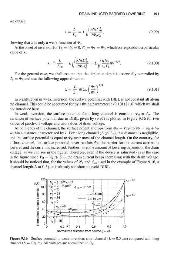
DRAIN INDUCED BARRIER LOWERING 191
we obtain
λ =L
Lc
= L 4
√
q NbC2ox
2Ψsǫ3si
, (9.99)
showing that λ is only a weak function of Ψs.
At the onset of inversion for VS = VD = 0, Ψs = ΨP = Ψ0, which corresponds to a particular
value of λ:
λ0 L
Lc0
= L 4
√
q NbC2ox
2Ψ0ǫ3si
= L
√
q Nb
ǫsiΓb
Ψ−1/40 . (9.100)
For the general case, we shall assume that the depletion depth is essentially controlled by
Ψs = ΨP and use the following approximation:
λ =L
Lc
∼= λ0
(
Ψ0
ΨP
)1/4
. (9.101)
In reality, even in weak inversion, the surface potential with DIBL is not constant all along
the channel. This could be accounted for by a fitting parameter in (9.101) [116] which we shall
not introduce here.
In weak inversion, the surface potential for a long channel is constant: Ψsl = ΨP. The
variation of surface potential due to DIBL given by (9.97) is plotted in Figure 9.16 for two
values of pinch-off voltage and two values of drain voltage.
At both ends of the channel, the surface potential drops from ΦB + VS,D to ΨP = Ψ0 + VP
within a distance characterized by λ. For a long channel (L ≫ Lc), this distance is negligible,
and the surface potential is equal to ΨP over most of the channel length. On the contrary, for
a short channel, the surface potential never reaches ΨP; the barrier for the current carriers is
lowered and the current is increased. Furthermore, the amount of lowering depends on the drain
voltage, as we can see in the figure. Therefore, even if the device is saturated (as is the case
in the figure since VD − VS ≫ UT), the drain current keeps increasing with the drain voltage.
It should be noticed that, for the values of Nb and Cox used in the example of Figure 9.16, a
channel length L = 0.5 μm is already too short to avoid DIBL.
0
20
40
60
80
100
120
0 0.2 0.4 0.6 0.8 1.0
vd = 40
vd = 80
y0 = 32
fB = 36
Nb = 3.1016 cm–3
vs = 0
Lc0 = 96 nmCox = 2.1 fF/µm2
(gb = 3)
ys (x)
Norm
aliz
ed s
urf
ace p
ote
ntia
l
Normalized distance from source x = x/L
vp = –15
vp = –5
L = 0.5 µm
L = 10 µm
∆ys(x)
∆ysmin
x0
Figure 9.16 Surface potential in weak inversion: short channel (L = 0.5 μm) compared with long
channel (L = 10 μm). All voltages are normalized to UT
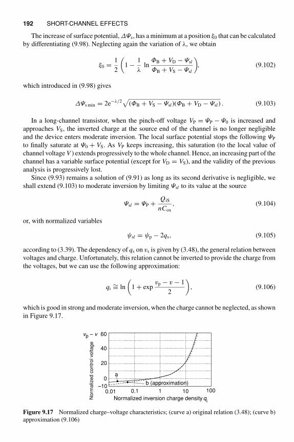
192 SHORT-CHANNEL EFFECTS
The increase of surface potential, ΔΨs, has a minimum at a position ξ0 that can be calculated
by differentiating (9.98). Neglecting again the variation of λ, we obtain
ξ0 =1
2
(
1 −1
λln
ΦB + VD − Ψsl
ΦB + VS − Ψsl
)
, (9.102)
which introduced in (9.98) gives
ΔΨs min = 2e−λ/2√
(ΦB + VS − Ψsl)(ΦB + VD − Ψsl) . (9.103)
In a long-channel transistor, when the pinch-off voltage VP = ΨP − Ψ0 is increased and
approaches VS, the inverted charge at the source end of the channel is no longer negligible
and the device enters moderate inversion. The local surface potential stops the following ΨP
to finally saturate at Ψ0 + VS. As VP keeps increasing, this saturation (to the local value of
channel voltage V ) extends progressively to the whole channel. Hence, an increasing part of the
channel has a variable surface potential (except for VD = VS), and the validity of the previous
analysis is progressively lost.
Since (9.93) remains a solution of (9.91) as long as its second derivative is negligible, we
shall extend (9.103) to moderate inversion by limiting Ψsl to its value at the source
Ψsl = ΨP +QiS
nCox
, (9.104)
or, with normalized variables
ψsl = ψp − 2qs, (9.105)
according to (3.39). The dependency of qs on vs is given by (3.48), the general relation between
voltages and charge. Unfortunately, this relation cannot be inverted to provide the charge from
the voltages, but we can use the following approximation:
qi∼= ln
(
1 + expvp − v − 1
2
)
, (9.106)
which is good in strong and moderate inversion, when the charge cannot be neglected, as shown
in Figure 9.17.
–10
60
0
20
40
100100.01 0.1 1
Normalized inversion charge density qi
vp – v
No
rma
lize
d c
on
tro
l vo
lta
ge
a
b (approximation)
Figure 9.17 Normalized charge–voltage characteristics; (curve a) original relation (3.48); (curve b)
approximation (9.106)
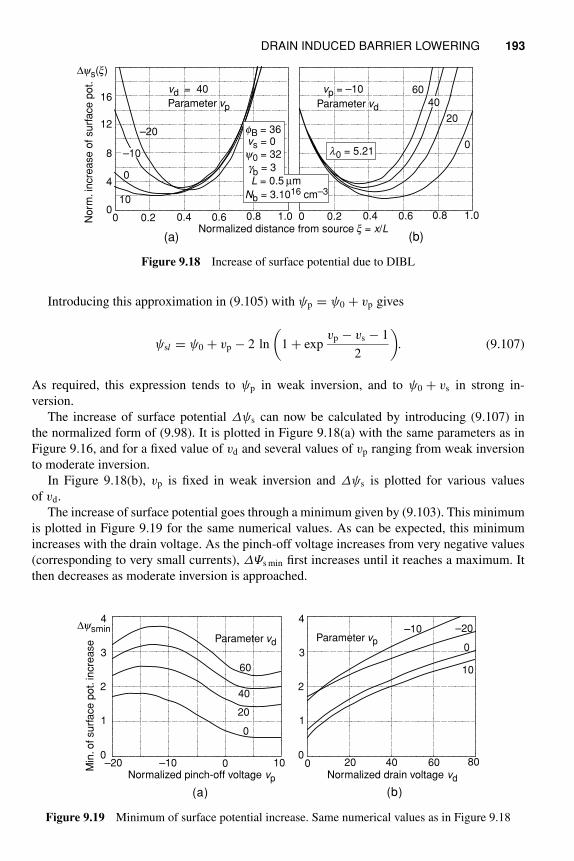
DRAIN INDUCED BARRIER LOWERING 193
–20
0
Parameter vp
vd = 40
10
–10
0
4
8
12
16
∆ys(x)
No
rm. in
cre
ase
of
su
rfa
ce
po
t.
0 0.2 0.4 0.6 0.8 1.0
(a)
Parameter vd
vp = –10
Normalized distance from source x = x/L(b)
0
20
60
l0 = 5.21
40
0 0.2 0.4 0.6 0.8 1.0
y0 = 32
fB = 36
gb = 3
vs = 0
L = 0.5 µm
Nb = 3.1016 cm–3
Figure 9.18 Increase of surface potential due to DIBL
Introducing this approximation in (9.105) with ψp = ψ0 + vp gives
ψsl = ψ0 + vp − 2 ln
(
1 + expvp − vs − 1
2
)
. (9.107)
As required, this expression tends to ψp in weak inversion, and to ψ0 + vs in strong in-
version.
The increase of surface potential Δψs can now be calculated by introducing (9.107) in
the normalized form of (9.98). It is plotted in Figure 9.18(a) with the same parameters as in
Figure 9.16, and for a fixed value of vd and several values of vp ranging from weak inversion
to moderate inversion.
In Figure 9.18(b), vp is fixed in weak inversion and Δψs is plotted for various values
of vd.
The increase of surface potential goes through a minimum given by (9.103). This minimum
is plotted in Figure 9.19 for the same numerical values. As can be expected, this minimum
increases with the drain voltage. As the pinch-off voltage increases from very negative values
(corresponding to very small currents), ΔΨs min first increases until it reaches a maximum. It
then decreases as moderate inversion is approached.
–20
0
1
2
3
0
4
Parameter vp
600 20 40 80
Normalized drain voltage vd
10
–10
(b)
–20 –10 0 10
(a)
Normalized pinch-off voltage vp
1
2
3
0
4
Min
. o
f su
rfa
ce
po
t. in
cre
ase
∆ysminParameter vd
60
40
20
0
Figure 9.19 Minimum of surface potential increase. Same numerical values as in Figure 9.18
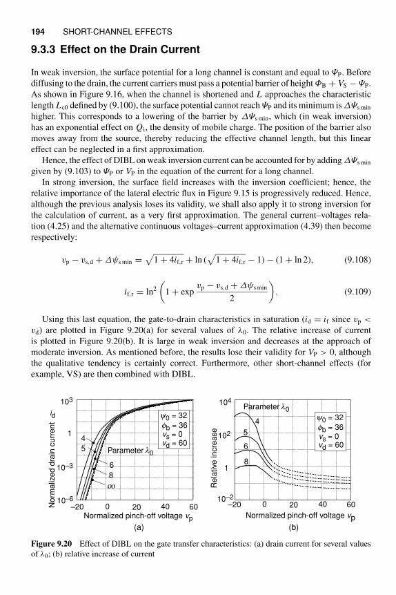
194 SHORT-CHANNEL EFFECTS
9.3.3 Effect on the Drain Current
In weak inversion, the surface potential for a long channel is constant and equal to ΨP. Before
diffusing to the drain, the current carriers must pass a potential barrier of height ΦB + VS − ΨP.
As shown in Figure 9.16, when the channel is shortened and L approaches the characteristic
length Lc0 defined by (9.100), the surface potential cannot reach ΨP and its minimum is ΔΨs min
higher. This corresponds to a lowering of the barrier by ΔΨs min, which (in weak inversion)
has an exponential effect on Qi, the density of mobile charge. The position of the barrier also
moves away from the source, thereby reducing the effective channel length, but this linear
effect can be neglected in a first approximation.
Hence, the effect of DIBL on weak inversion current can be accounted for by adding ΔΨs min
given by (9.103) to ΨP or VP in the equation of the current for a long channel.
In strong inversion, the surface field increases with the inversion coefficient; hence, the
relative importance of the lateral electric flux in Figure 9.15 is progressively reduced. Hence,
although the previous analysis loses its validity, we shall also apply it to strong inversion for
the calculation of current, as a very first approximation. The general current–voltages rela-
tion (4.25) and the alternative continuous voltages–current approximation (4.39) then become
respectively:
vp − vs,d + Δψs min =√
1 + 4if,r + ln (√
1 + 4if,r − 1) − (1 + ln 2), (9.108)
if,r = ln2
(
1 + expvp − vs,d + Δψs min
2
)
. (9.109)
Using this last equation, the gate-to-drain characteristics in saturation (id = if since vp <
vd) are plotted in Figure 9.20(a) for several values of λ0. The relative increase of current
is plotted in Figure 9.20(b). It is large in weak inversion and decreases at the approach of
moderate inversion. As mentioned before, the results lose their validity for VP > 0, although
the qualitative tendency is certainly correct. Furthermore, other short-channel effects (for
example, VS) are then combined with DIBL.
103
10–3
1
10–6
No
rma
lize
d d
rain
cu
rre
nt
id
5
6
8
oo
vs = 0vd = 60
y0 = 32
fb = 36
Parameter l0
Normalized pinch-off voltage vp
–20 0 20 40 60
(a)
4
–20 0 20 40 60
104
102
10–2
1
Re
lative
in
cre
ase
vs = 0vd = 60
y0 = 32
fb = 36
Parameter l0
4
5
6
8
Normalized pinch-off voltage vp
(b)
Figure 9.20 Effect of DIBL on the gate transfer characteristics: (a) drain current for several values
of λ0; (b) relative increase of current
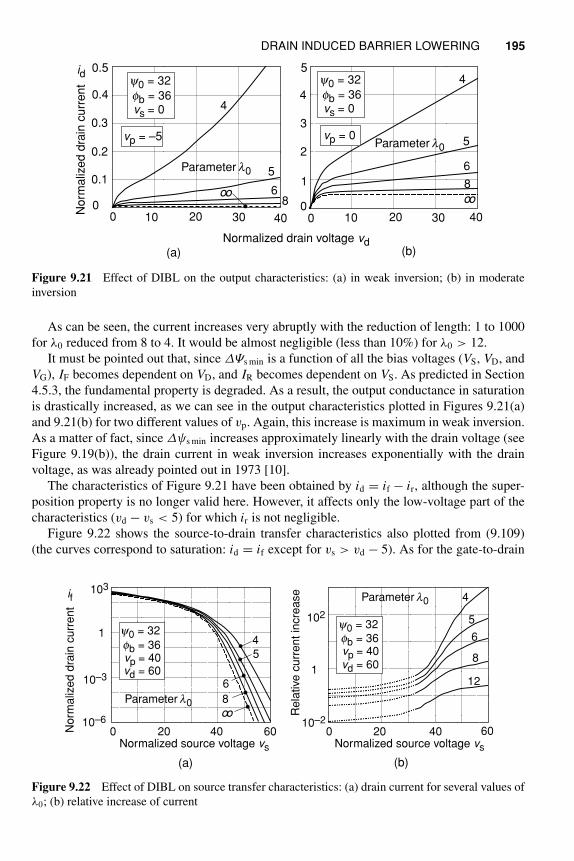
DRAIN INDUCED BARRIER LOWERING 195
Normalized drain voltage vd
Norm
aliz
ed d
rain
curr
ent
id
0
0.5
0 40
vs = 0
y0 = 32
fb = 36
0.1
0.2
0.3
0.4
10 20 30
oo
vp = –5
4
5
68
Parameter l0
0
5
040
1
2
3
4
10 20 30
vs = 0
y0 = 32
fb = 36
vp = 0Parameter l0
4
5
6
8
oo
(a) (b)
Figure 9.21 Effect of DIBL on the output characteristics: (a) in weak inversion; (b) in moderate
inversion
As can be seen, the current increases very abruptly with the reduction of length: 1 to 1000
for λ0 reduced from 8 to 4. It would be almost negligible (less than 10%) for λ0 > 12.
It must be pointed out that, since ΔΨs min is a function of all the bias voltages (VS, VD, and
VG), IF becomes dependent on VD, and IR becomes dependent on VS. As predicted in Section
4.5.3, the fundamental property is degraded. As a result, the output conductance in saturation
is drastically increased, as we can see in the output characteristics plotted in Figures 9.21(a)
and 9.21(b) for two different values of vp. Again, this increase is maximum in weak inversion.
As a matter of fact, since Δψs min increases approximately linearly with the drain voltage (see
Figure 9.19(b)), the drain current in weak inversion increases exponentially with the drain
voltage, as was already pointed out in 1973 [10].
The characteristics of Figure 9.21 have been obtained by id = if − ir, although the super-
position property is no longer valid here. However, it affects only the low-voltage part of the
characteristics (vd − vs < 5) for which ir is not negligible.
Figure 9.22 shows the source-to-drain transfer characteristics also plotted from (9.109)
(the curves correspond to saturation: id = if except for vs > vd − 5). As for the gate-to-drain
0 6020 4010–2
102
1
Parameter l0
Rela
tive
curr
ent in
cre
ase
Normalized source voltage vs
vp = 40vd = 60
y0 = 32
fb = 36
4
5
6
8
12
0 20 40 60Normalized source voltage vs
10–6
Norm
aliz
ed d
rain
curr
ent
if
4
5
6
8
oo
103
10–3
1
vp = 40vd = 60
y0 = 32
fb = 36
Parameter l0
(a) (b)
Figure 9.22 Effect of DIBL on source transfer characteristics: (a) drain current for several values of
λ0; (b) relative increase of current
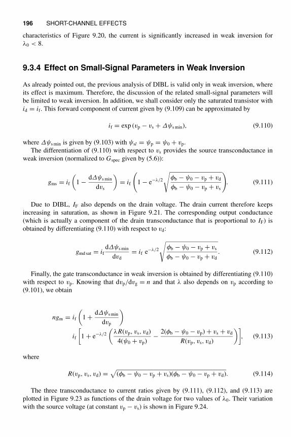
196 SHORT-CHANNEL EFFECTS
characteristics of Figure 9.20, the current is significantly increased in weak inversion for
λ0 < 8.
9.3.4 Effect on Small-Signal Parameters in Weak Inversion
As already pointed out, the previous analysis of DIBL is valid only in weak inversion, where
its effect is maximum. Therefore, the discussion of the related small-signal parameters will
be limited to weak inversion. In addition, we shall consider only the saturated transistor with
id = if. This forward component of current given by (9.109) can be approximated by
if = exp (vp − vs + Δψs min), (9.110)
where Δψs min is given by (9.103) with ψsl = ψp = ψ0 + vp.
The differentiation of (9.110) with respect to vs provides the source transconductance in
weak inversion (normalized to Gspec given by (5.6)):
gms = if
(
1 −dΔψs min
dvs
)
= if
(
1 − e−λ/2
√
φb − ψ0 − vp + vd
φb − ψ0 − vp + vs
)
. (9.111)
Due to DIBL, IF also depends on the drain voltage. The drain current therefore keeps
increasing in saturation, as shown in Figure 9.21. The corresponding output conductance
(which is actually a component of the drain transconductance that is proportional to IF) is
obtained by differentiating (9.110) with respect to vd:
gmd sat = if
dΔψs min
dvd
= if e−λ/2
√
φb − ψ0 − vp + vs
φb − ψ0 − vp + vd
. (9.112)
Finally, the gate transconductance in weak inversion is obtained by differentiating (9.110)
with respect to vp. Knowing that dvp/dvg = n and that λ also depends on vp according to
(9.101), we obtain
ngm = if
(
1 +dΔψs min
dvp
)
if
[
1 + e−λ/2
(
λR(vp, vs, vd)
4(ψ0 + vp)−
2(φb − ψ0 − vp) + vs + vd
R(vp, vs, vd)
)]
, (9.113)
where
R(vp, vs, vd) =√
(φb − ψ0 − vp + vs)(φb − ψ0 − vp + vd). (9.114)
The three transconductance to current ratios given by (9.111), (9.112), and (9.113) are
plotted in Figure 9.23 as functions of the drain voltage for two values of λ0. Their variation
with the source voltage (at constant vp − vs) is shown in Figure 9.24.
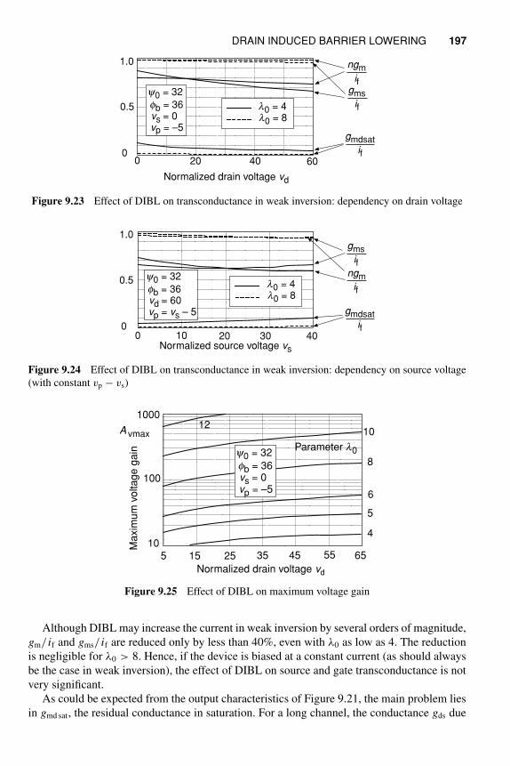
DRAIN INDUCED BARRIER LOWERING 197
gms
if
ngm
if
gmdsat
if
l0 = 4l0 = 8vs = 0
vp = –5
y0 = 32
fb = 36
0 20 40 600
0.5
1.0
Normalized drain voltage vd
Figure 9.23 Effect of DIBL on transconductance in weak inversion: dependency on drain voltage
gms
ifngm
if
gmdsat
if0
0.5
1.0
0 10 20 30 40
l0 = 4l0 = 8
vd = 60vp = vs – 5
y0 = 32
fb = 36
Normalized source voltage vs
Figure 9.24 Effect of DIBL on transconductance in weak inversion: dependency on source voltage
(with constant vp − vs)
5 15 25 35 45 55 65
Normalized drain voltage vd
10
100
1000
Maxim
um
voltage g
ain
A vmax
4
5
6
8
10
Parameter l0
12
vs = 0vp = –5
y0 = 32
fb = 36
Figure 9.25 Effect of DIBL on maximum voltage gain
Although DIBL may increase the current in weak inversion by several orders of magnitude,
gm/ if and gms/ if are reduced only by less than 40%, even with λ0 as low as 4. The reduction
is negligible for λ0 > 8. Hence, if the device is biased at a constant current (as should always
be the case in weak inversion), the effect of DIBL on source and gate transconductance is not
very significant.
As could be expected from the output characteristics of Figure 9.21, the main problem lies
in gmd sat, the residual conductance in saturation. For a long channel, the conductance gds due
198 SHORT-CHANNEL EFFECTS
to CLM is much smaller than gms; therefore, the small-signal voltage gain given by (5.24) can
be very large. With the DIBL occurring in a short channel, the voltage gain is limited to
Av max =Gms
Gmd sat
=gms
gmd sat
. (9.115)
As shown by Figure 9.25, this maximum gain becomes very small for λ0 = 4. It increases
rapidly for larger values of λ0 to be limited by CLM for λ0 larger than 10–12.
9.4 SHORT-CHANNEL THERMAL NOISE MODEL
The long-channel thermal noise model derived in Section 6.2 assumed that the mobility was
constant along the channel and that the channel length was sufficiently long so that VS and
CLM could be neglected. These assumptions are obviously not valid anymore for short-channel
devices where VS and CLM effects have to be accounted for. Mobility reduction due to the
vertical field also greatly influences the thermal noise and has also to be included. This will be
done in the next sections.
9.4.1 Thermal Noise Drain Conductance
In order to account for the CLM, the region between the source and the drain is split into the
channel region of length Leff on the source side, where the carrier velocity is not saturated, and
the VS region on the drain side, where the carrier velocity saturates to vsat (Figure 9.26). Since
in the VS region the carrier travel at their maximum saturated velocity, they will not respond
to the local change of the electric field caused by the noise voltage fluctuations. Therefore,
the noise fluctuations generated in the VS region do not propagate to the drain since the
conductance on the drain side is zero [117]. Therefore, the dominant contribution to the drain
noise mainly comes from the channel region between x = 0 and x = Leff.
Since the effects of VS, mobility reduction due to the vertical field, and CLM are pre-
dominant in strong inversion, we will derive the PSD (power spectral density) of the drain
L
Leff
Gs Gd
x
x
Leff – x
Figure 9.26 Cross section of the MOS channel with a thermal noise source at position x and with
the VS region to account for the effect of CLM
SHORT-CHANNEL THERMAL NOISE MODEL 199
current fluctuations assuming that the transistor is biased in strong inversion. The model can
be extended to cover all regions of operation as described in [55].
We will reuse the general approach presented in Section 6.1. The PSD of the drain current
fluctuations due to the single elementary noise source δ In is given by (6.3), which is repeated
here for convenience:
Sδ I 2D
= G2chΔR2SδI 2
n,
where ΔR is the resistance across the channel slice and Gch is the channel conductance at
point x along the channel and given by (6.2)
1
Gch
1
Gs
+1
Gd
. (9.116)
Conductances Gs and Gd are the channel conductances seen by the local thermal noise current
source δ In on the source and drain sides respectively. They can be derived by splitting the total
transistor into transistor M1 and M2 on the source and drain side, respectively, as shown in
Figures 6.2 and 6.3. Conductance Gs actually corresponds to the drain transconductance of
transistor M1 after having isolated it from transistor M2:
Gs = Gmd1 dID
dV, (9.117)
where current ID is redefined as the current entering the drain of transistor M1:
ID =W
x
∫ V
VS
(−Qi)μeff dV ′. (9.118)
Notice that for clarity, V ′ is used as dummy variable for integration in (9.118) to distinguish
it from variable V. In order to differentiate (9.118) for calculating conductance Gs, we must
remember that μeff is a function of the electric field Ex which depends on the position x along
the channel or equivalently on the channel voltage V at that position. In the most general case,
we do not know μeff as a function of the channel voltage. Even though we would know it, it is
not sure we could integrate (9.118). A work around is to notice that the current ID given by
ID = −W [−Qi(V )]μeff(Ex )Ex (9.119)
is constant along the channel and (9.119) can be solved for Ex , which now becomes a function
of V and ID. Replacing Ex = Ex (V, ID) in the expression of μeff makes μeff become a function
of V and ID and (9.119) becomes
ID = −W [−Qi(V )]μeff(V, ID)Ex
= W [−Qi(V )]μeff(V, ID)dV
dx.
(9.120)
The current ID is then given by a function F(V, ID) of variables V and ID defined by
ID = F(V, ID) W
x
∫ V
VS
[−Qi(V′)]μeff(V
′, ID) dV ′. (9.121)
200 SHORT-CHANNEL EFFECTS
The total differential of current ID is then given by
dID = dF =∂F
∂VdV +
∂F
∂ID
dID, (9.122)
and the total derivative corresponding to Gs writes
Gs =dID
dV=
∂F
∂V+
∂F
∂ID
dID
dV, (9.123)
which can be solved for Gs = dID/dV as
Gs =dID
dV=
∂F∂V
1 − ∂F∂ID
. (9.124)
The partial derivatives of F can be evaluated from (9.121) as
∂F
∂V=
W
x(−Qi)µeff, (9.125a)
∂F
∂ID
=W
x
∫ V
VS
(−Qi)∂µeff
∂ID
dV ′. (9.125b)
Replacing (9.125a) and (9.125b) in (9.124) results in [54]
Gs =W (−Qi)µeff
x − W∫ V
VS(−Qi)
∂µeff
∂IDdV ′
. (9.126)
In order to evaluate ∂µeff/∂ ID, we notice that
∂µeff
∂ID
=∂µeff
∂Ex
∂Ex
∂ID
= µ′eff
∂Ex
∂ID
, (9.127)
where
µ′eff
∂µeff
∂ Ex
. (9.128)
From (9.120), we have
∂ID
∂Ex
= −W (−Qi)(
µeff + µ′eff Ex
)
= −W (−Qi)µdiff, (9.129)
where µdiff is the differential mobility defined by (9.3) and which can be written as
µdiff =dvdrift
dEx
=d(µeff Ex )
dEx
= µeff + µ′eff Ex . (9.130)
SHORT-CHANNEL THERMAL NOISE MODEL 201
Hence
∂µeff
∂ID
=µ′
eff
−W (−Qi)µdiff
. (9.131)
Replacing (9.131) in (9.126) finally results in [54]
Gs =W (−Qi)µeff
x +∫ V
VS
µ′eff
µdiffdV ′
. (9.132)
Conductance Gd corresponds to the source transconductance of transistor M2 and is defined
as
Gd = Gms2 −dID
dV. (9.133)
with the current ID defined as
ID =W
Leff − x
∫ VDeff
V
(−Qi)µeff dV ′, (9.134)
where saturation at the drain and CLM were accounted for by defining Leff and VDeff as
Leff =
L for VD < VD sat
L − ΔL for VD ≥ VD sat,(9.135)
where ΔL is the channel reduction due CLM, and
VDeff =
VD for VD < VD sat
VD sat for VD ≥ VD sat.(9.136)
Conductance Gd is then obtained in a similar way than Gs leading to
Gd =W (−Qi)μeff
(Leff − x) +∫ VDeff
V
μ′eff
μdiffdV ′
. (9.137)
The channel conductance Gch at a position x is then easily obtained from (9.116), (9.132),
and (9.137) as [54]
Gch =W (−Qi)μeff
Leff +∫ VDeff
VS
μ′eff
μdiffdV ′
. (9.138)
The channel slice resistance ΔR can be calculated in a similar way than Gd, but integrating
from x to x + Δx instead of L (or Leff in saturation). After noticing that the voltage drop
202 SHORT-CHANNEL EFFECTS
between x and x + Δx is simply equal to ΔV = −ExΔx , we get [54]
1
ΔR= ΔG =
W (−Qi)μeff
Δx − μ′eff
μdiffExΔx
=W (−Qi)μdiff
Δx. (9.139)
Here, we would like to point out that in case of a long-channel MOS transistor, μeff is
independent of the electric field Ex and hence μ′eff = 0. Conductance Gch and resistance ΔR
then reduce to
Gch = μeff(−Qi)W
Leff
=W (−Qi)μeff
Leff
, (9.140a)
ΔR =Δx
Wμeff(−Qi), (9.140b)
which correspond to the expressions (6.9) and (6.10), respectively, which were derived in
Section 6.1 for the thermal noise of a long-channel device.
Calculation of the current noise source between x and x + Δx is a difficult task. This
is because, in presence of an electric field, the segment is no longer in equilibrium and in
nonequilibrium, the Einstein relation is no longer valid. The method to model device noise in
nonequilibrium is to assume that even in nonequilibrium an Einstein-like relation holds between
the mobility and the diffusivity Dn (of electrons). One needs to be careful with definitions
when making this transition because it often acts as a source of error. The procedure is to
define [118–121]
Dn =kTnμdiff
q, (9.141)
where Tn is defined as the noise temperature. Since Dn is unknown in nonequilibrium, this
relationship in general provides nothing new but a definition of Tn. Note that in most of the
cases the noise temperature Tn is different from the carrier temperature TC [118].
It is shown in [118] that Tn becomes equal to TC when the velocity distribution is heated
Maxwellian. It is to be noted that we are considering the inversion layer of the MOS transistor
where the carrier density is in the order of 1018 cm−3 and that kind of carrier concentration
thermalize the distribution function and enforces it to be heated Maxwellian (we are assuming
the channel to be nondegenerate) [122–124]. This observation provides a great simplification
by expressing diffusivity Dn in terms of known quantities. It allows to write the expression of
SδI 2n
as [54, 119]
SδI 2n
= 4qW (−Qi)Dn
Δx= 4kTC
W (−Qi)μdiff
Δx= 4kTCΔG, (9.142)
where the expression of ΔG given by (9.139) has been used.
It is important to point out that many publications about numerical noise simulation [125–
127] as well as [128] use the cord mobility μeff instead of the differential mobility μdiff when
replacing the diffusivity. Ref. [128] has also made an additional assumption that the decrease in
cord mobility is exactly balanced by the increase in temperature leaving the diffusivity about
constant. Device simulations made for a typical 0.18 μm N-channel MOS transistor show
that the product of the cord mobility times the carrier temperature is actually not constant
SHORT-CHANNEL THERMAL NOISE MODEL 203
but increases monotonically from source to drain [54]. This indicates that the increase in
temperature is not fully compensated by the decrease in cord mobility.
In order to define a noise conductance, (9.142) can be written as
SδI 2n
= 4kTL
TC
TL
ΔG, (9.143)
where TL is the lattice temperature. The PSD of the drain current fluctuations due to δ In is then
given by
SδI 2D
= 4kTL
TC
TL
G2chΔR. (9.144)
Replacing Gch by (9.138) and ΔR by the inverse of (9.139) results in [54]
SδI 2D
= 4kTL MW
L2eff
TC
TL
μ2eff
μdiff
(−Qi)Δx, (9.145)
where [54]
M 1
(
1 + 1Leff
∫ VDeff
Vs
μ′eff
μdiffdV
)2. (9.146)
The PSD of the total noise current fluctuation at the drain SΔI 2D
can be derived by integrating
the PSD due to an elementary contribution SδI 2D
at position x over the channel assuming that
the contribution of each slice at different positions along the channel remains uncorrelated.
This leads to [54]
SΔI 2D
= 4kTL MW
L2eff
∫ Leff
0
TC
TL
μ2eff
μdiff
(−Qi) dx, (9.147)
which can be written as
SΔI 2D
4kTLGnD, (9.148)
and where GnD is the thermal noise conductance at the drain given by
GnD = MW
L2eff
∫ Leff
0
TC
TL
μ2eff
μdiff
(−Qi) dx . (9.149)
Equation (9.149) is very general and does not depend on a particular velocity-field (or
mobility-field) model. Nevertheless, the relation between the carrier temperature TC and the
lattice temperature TL has to be consistent with the field-dependent mobility model. It can be
shown that the third velocity-field model (Model 3), which is also used for deriving the channel
length reduction ΔL in Section 9.2, actually arises as an approximation of [122, 123, 129]
μeff = μz
√
TL
TC
, (9.150)
204 SHORT-CHANNEL EFFECTS
which gives the relation between carrier temperature and mobility as
TC
TL
=(
µz
µeff
)2
=
⎧
⎪
⎨
⎪
⎩
(
1 + |Ex |2Ec
)2
for |Ex | < 2Ec
( |Ex |Ec
)2
for |Ex | ≥ 2Ec.
(9.151)
Using that same mobility-field relation (9.15), we can deduce the following relations:
µ′eff
µdiff
=µ′
eff
µeff + µ′eff Ex
= −1
2Ec
(9.152)
and
µ2eff
µdiff
=µ2
eff
µeff + µ′eff Ex
= µz . (9.153)
Note that relations (9.152) and (9.153) are valid only for |Ex | < 2Ec and can be applied only
in the nonsaturation region comprised between x and Leff where |Ex | reaches 2Ec and vdrift
becomes equal to vsat. Anyway, as was pointed out earlier, the contribution of the VS region
to the total drain noise is null since in the third velocity-field model, the differential mobility
is null and therefore, according to (9.139), no noise is produced.
Introducing (9.152) into (9.146), the M factor then simply reduces to
M =1
(
1 − VDeff−VS
2Leff·Ec
)2, (9.154)
whereas using (9.153) in (9.149), GnD becomes
GnD = MW
L2eff
∫ Leff
0
µz
TC
TL
(−Qi(x))dx (9.155)
again valid for |Ex | < 2Ec, i.e. in the non-saturation region. The effect of mobility reduction
due to the vertical field has been discussed in Section 8.2 and is modelled by (8.5). Although
the mobility given by (8.5) is a local mobility and includes qi which depends on the position
x along the channel, an effective mobility can be approximated by replacing qi in (8.5) by an
average charge (qs + qd)/2. The mobility µz can then be taken out of the integral in (9.155),
leading to
GnD = Mµz
W
L2eff
∫ Leff
0
TC
TL
(−Qi(x))dx
= Mµz
W
L2eff
∫ Leff
0
(
µz
µeff
)2
(−Qi(x))dx
= Mµz
W
L2eff
∫ Leff
0
(
1 +|Ex |
2Ec
)2
(−Qi(x))dx,
(9.156)
where (9.151) has been used.
SHORT-CHANNEL THERMAL NOISE MODEL 205
Notice that for a long-channel MOS transistor, µeff is independent of the electric field Ex and
equal to the mobility at low longitudinal field µeff = µz and hence µ′eff = 0 and the differential
mobility is equal to the cord mobility µdiff = µeff = µz . The carrier temperature TC is then
equal to the lattice temperature TL and the effective length Leff is approximately equal to the
source-to-drain length L . Factor M is then simply equal to unity and (9.149) and (9.155) then
simplify to
GnD = µz
W
L2
∫ L
0
[−Qi(x)] dx, (9.157)
which corresponds to the long-channel expression (6.15) obtained earlier in Section 6.2.
As shown in (9.150), the effect of VS cannot be considered without the effect of carrier
heating. On the other hand, the effect of mobility reduction due to the vertical field and CLM
can be considered separately. This will be done in the next sections.
9.4.2 Effect of VS and Carrier Heating on Thermal Noise
In this section we will assume that the effects of mobility reduction due to the vertical field
and CLM can be neglected and we will concentrate on the combined effect of VS and carrier
heating. This means that µz = µ0 and Leff = L . To this purpose we will again use the third
velocity-field model (Model 3) defined in (9.15) or its normalized form (9.16).
The drain thermal noise conductance accounting for VS and carrier heating only is given
by (9.155) with Leff = L and µz = µ01
GnD(VS+CH) = Mµ0
W
L2
∫ L
0
(
1 +|Ex |
2Ec
)2
[−Qi(x)] dx, (9.158)
or in normalized form
gnD(VS+CH) GnD(VS+CH)
Gspec
= M
∫ 1
0
[
1 +e(ξ )
2
]2
qi(ξ ) dξ, (9.159)
where e is the normalized longitudinal field defined by (9.6) and
M =1
(
1 − VDeff−VS
2L Ec
)2. (9.160)
gnD(VS+CH) can be split into two components gnD(VS) and gnD(CH):
gnD(VS+CH) = gnD(VS) + gnD(CH), (9.161)
where gnD(VS) accounts for the effects of VS only and is given by
gnD(VS) = M
∫ 1
0
qidξ = MqI, (9.162)
1 The fact that only the VS and carrier heating effects are accounted for is indicated by the sign (VS + CH) at the end
of the subscript.
206 SHORT-CHANNEL EFFECTS
whereas gnD(CH) accounts for the additional effect of carrier heating and is given by
gnD(CH) = M
∫ 1
0
[
e(ξ ) +(
e(ξ )
2
)2]
qi(ξ ) dξ, (9.163)
Note that even though the integral in (9.162) is the same expression as obtained for the
long-channel case, the inversion charge distribution along the channel when VS occurs can
be quite different from that without VS as in the long-channel case. Therefore gnD(VS) is not
simply equal to M times the long-channel value of gnD as (9.161) might wrongly suggest.
For vd ≤ vd sat, the normalized noise conductances gnD(VS) and gnD(CH) can be found by
operating a change of variable from ξ to qi using (9.22) and (9.36) with the definitions of the
normalized velocity ν and mobility u given by (9.14) and (9.16) respectively. This results in
expressions for dqi/dξ and e given by
dqi
dξ=
−id
2qi − λc
2id
, (9.164a)
e =λcid
2qi − λc
2id
, (9.164b)
where id is given by (9.47). gnD(VS) then becomes
gnD(VS) =M
id
∫ qs
qd
qi
(
2qi +λc
2id
)
dqi
=M
id
[
2
3
(
q3s − q3
d
)
−λcid
4
(
q2s − q2
d
)
]
. (9.165)
Similarly, gnD(CH) is obtained by replacing in (9.163) e by (9.164b) and dξ by dqi given by
(9.164a), resulting in
gnD(CH) = Mλc
2
[
q2s − q2
d +λcid
4(qs − qd)
+
(
λcid
4
)2
ln
(
qs − λc/4id
qd − λc/4id
)
]
. (9.166)
For vd ≥ vd sat, gnD(VS) = gnD sat(VS), and gnD(CH) = gnD sat(CH) which can be obtained by
replacing id and qd in (9.165) and (9.166) by (9.49b) and (9.49a) respectively.
The corresponding thermal noise parameter can also be split into two components according
to
δnD(VS+CH) = δnD(VS) + δnD(CH), (9.167)
where δnD(VS) gnD(VS)/qs and δnD(CH) gnD(CH)/qs.
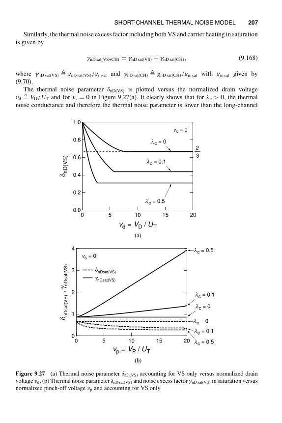
SHORT-CHANNEL THERMAL NOISE MODEL 207
Similarly, the thermal noise excess factor including both VS and carrier heating in saturation
is given by
γnD sat(VS+CH) = γnD sat(VS) + γnD sat(CH), (9.168)
where γnD sat(VS) gnD sat(VS)/gmsat and γnD sat(CH) gnD sat(CH)/gm sat with gm sat given by
(9.70).
The thermal noise parameter δnD(VS) is plotted versus the normalized drain voltage
vd VD/UT and for vs = 0 in Figure 9.27(a). It clearly shows that for λc > 0, the thermal
noise conductance and therefore the thermal noise parameter is lower than the long-channel
1.0
0.8
0.6
0.4
0.2
0.0
δ nD
(VS
)
20151050
vd = VD / UT
2
3
lc = 0
lc = 0.1
lc = 0.5
vs = 0
4
3
2
1
0
δ nD
sat(
VS
) ,
g nD
sat(
VS
)
20151050
vp = VP / UT
lc = 0.5
lc = 0.1
lc = 0
lc = 0.5
lc = 0
lc = 0.1
δnDsat(VS)
gnDsat(VS)
vs = 0
(a)
(b)
Figure 9.27 (a) Thermal noise parameter δnD(VS) accounting for VS only versus normalized drain
voltage vd. (b) Thermal noise parameter δnD sat(VS) and noise excess factor γnD sat(VS) in saturation versus
normalized pinch-off voltage vp and accounting for VS only
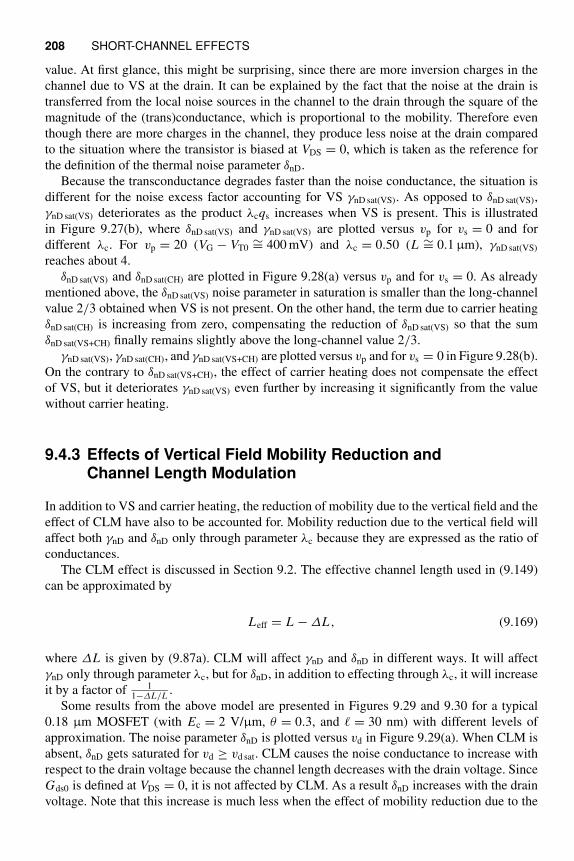
208 SHORT-CHANNEL EFFECTS
value. At first glance, this might be surprising, since there are more inversion charges in the
channel due to VS at the drain. It can be explained by the fact that the noise at the drain is
transferred from the local noise sources in the channel to the drain through the square of the
magnitude of the (trans)conductance, which is proportional to the mobility. Therefore even
though there are more charges in the channel, they produce less noise at the drain compared
to the situation where the transistor is biased at VDS = 0, which is taken as the reference for
the definition of the thermal noise parameter δnD.
Because the transconductance degrades faster than the noise conductance, the situation is
different for the noise excess factor accounting for VS γnD sat(VS). As opposed to δnD sat(VS),
γnD sat(VS) deteriorates as the product λcqs increases when VS is present. This is illustrated
in Figure 9.27(b), where δnD sat(VS) and γnD sat(VS) are plotted versus vp for vs = 0 and for
different λc. For vp = 20 (VG − VT0∼= 400 mV) and λc = 0.50 (L ∼= 0.1 μm), γnD sat(VS)
reaches about 4.
δnD sat(VS) and δnD sat(CH) are plotted in Figure 9.28(a) versus vp and for vs = 0. As already
mentioned above, the δnD sat(VS) noise parameter in saturation is smaller than the long-channel
value 2/3 obtained when VS is not present. On the other hand, the term due to carrier heating
δnD sat(CH) is increasing from zero, compensating the reduction of δnD sat(VS) so that the sum
δnD sat(VS+CH) finally remains slightly above the long-channel value 2/3.
γnD sat(VS), γnD sat(CH), and γnD sat(VS+CH) are plotted versus vp and for vs = 0 in Figure 9.28(b).
On the contrary to δnD sat(VS+CH), the effect of carrier heating does not compensate the effect
of VS, but it deteriorates γnD sat(VS) even further by increasing it significantly from the value
without carrier heating.
9.4.3 Effects of Vertical Field Mobility Reduction andChannel Length Modulation
In addition to VS and carrier heating, the reduction of mobility due to the vertical field and the
effect of CLM have also to be accounted for. Mobility reduction due to the vertical field will
affect both γnD and δnD only through parameter λc because they are expressed as the ratio of
conductances.
The CLM effect is discussed in Section 9.2. The effective channel length used in (9.149)
can be approximated by
Leff = L − ΔL , (9.169)
where ΔL is given by (9.87a). CLM will affect γnD and δnD in different ways. It will affect
γnD only through parameter λc, but for δnD, in addition to effecting through λc, it will increase
it by a factor of 11−ΔL/L
.
Some results from the above model are presented in Figures 9.29 and 9.30 for a typical
0.18 μm MOSFET (with Ec = 2 V/μm, θ = 0.3, and ℓ = 30 nm) with different levels of
approximation. The noise parameter δnD is plotted versus vd in Figure 9.29(a). When CLM is
absent, δnD gets saturated for vd ≥ vd sat. CLM causes the noise conductance to increase with
respect to the drain voltage because the channel length decreases with the drain voltage. Since
Gds0 is defined at VDS = 0, it is not affected by CLM. As a result δnD increases with the drain
voltage. Note that this increase is much less when the effect of mobility reduction due to the
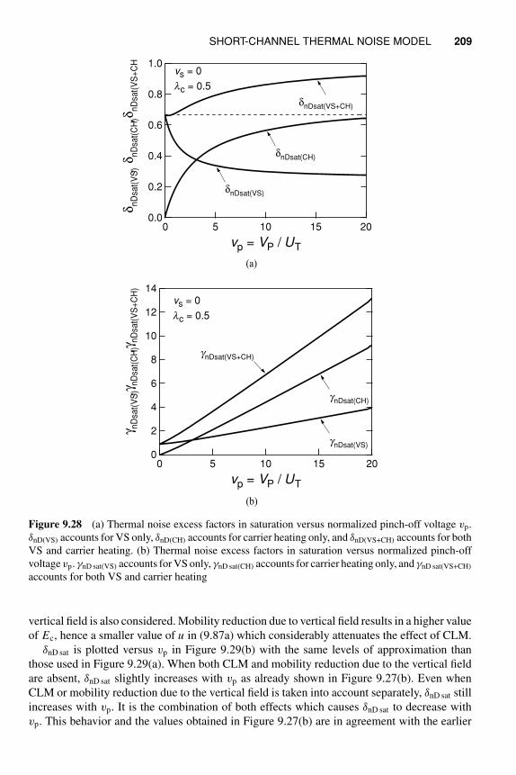
SHORT-CHANNEL THERMAL NOISE MODEL 209
1.0
0.8
0.6
0.4
0.2
0.0
δ nD
sat(
VS
) ,
δnD
sat(
CH
) , δ
nD
sat(
VS
+C
H
20151050
vp = VP / UT
δnDsat(VS)
δnDsat(CH)
δnDsat(VS+CH)
vs = 0
lc = 0.5
14
12
10
8
6
4
2
0
γ nD
sat(
VS
) ,
γ nD
sat(
CH
) ,
γ nD
sat(
VS
+C
H)
20151050
vp = VP / UT
vs = 0
lc = 0.5
gnDsat(VS)
gnDsat(CH)
gnDsat(VS+CH)
(a)
(b)
Figure 9.28 (a) Thermal noise excess factors in saturation versus normalized pinch-off voltage vp.
δnD(VS) accounts for VS only, δnD(CH) accounts for carrier heating only, and δnD(VS+CH) accounts for both
VS and carrier heating. (b) Thermal noise excess factors in saturation versus normalized pinch-off
voltage vp. γnD sat(VS) accounts for VS only, γnD sat(CH) accounts for carrier heating only, and γnD sat(VS+CH)
accounts for both VS and carrier heating
vertical field is also considered. Mobility reduction due to vertical field results in a higher value
of Ec, hence a smaller value of u in (9.87a) which considerably attenuates the effect of CLM.
δnD sat is plotted versus vp in Figure 9.29(b) with the same levels of approximation than
those used in Figure 9.29(a). When both CLM and mobility reduction due to the vertical field
are absent, δnD sat slightly increases with vp as already shown in Figure 9.27(b). Even when
CLM or mobility reduction due to the vertical field is taken into account separately, δnD sat still
increases with vp. It is the combination of both effects which causes δnD sat to decrease with
vp. This behavior and the values obtained in Figure 9.27(b) are in agreement with the earlier
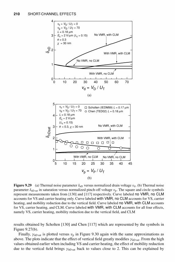
210 SHORT-CHANNEL EFFECTS
4
3
2
1
0
δ nD
706050403020100
vd = VD / UT
No VMR, no CLM
With VMR, with CLM
With VMR, no CLM
No VMR, with CLM
vs = VS / UT = 0
vg = VG / UT = 70
L = 0.18 µm
Ec = 2 V/µm (lc = 0.15)
q = 0.3
c = 30 nm
5
4
3
2
1
0
δ nD
sa
t
45403530252015105
vp = VP / UT
No VMR, no CLMWith VMR, no CLM
No VMR, with CLM
With VMR, with CLM
vs = VS / UT = 0
vd = VD / UT = 70
L = 0.18 µm
Ec = 2 V/µm
(lc = 0.15)
q = 0.3, c = 30 nm
Scholten (IEDM99) L = 0.17 µm
Chen (TED02) L = 0.18 µm
(a)
(b)
Figure 9.29 (a) Thermal noise parameter δnD versus normalized drain voltage vd. (b) Thermal noise
parameter δnD sat in saturation versus normalized pinch-off voltage vp. The square and circle symbols
represent measurements taken from [130] and [117] respectively. Curve labeled no VMR, no CLMaccounts for VS and carrier heating only. Curve labeled with VMR, no CLM accounts for VS, carrier
heating, and mobility reduction due to the vertical field. Curve labeled no VMR, with CLM accounts
for VS, carrier heating, and CLM. Curve labeled with VMR, with CLM accounts for all four effects,
namely VS, carrier heating, mobility reduction due to the vertical field, and CLM
results obtained by Scholten [130] and Chen [117] which are represented by the symbols in
Figure 9.27(b).
Finally, γnD sat is plotted versus vp in Figure 9.30 again with the same approximations as
above. The plots indicate that the effect of vertical field greatly modifies γnD sat. From the high
values obtained earlier when including VS and carrier heating, the effect of mobility reduction
due to the vertical field brings γnD sat back to values close to 2. This can be explained by
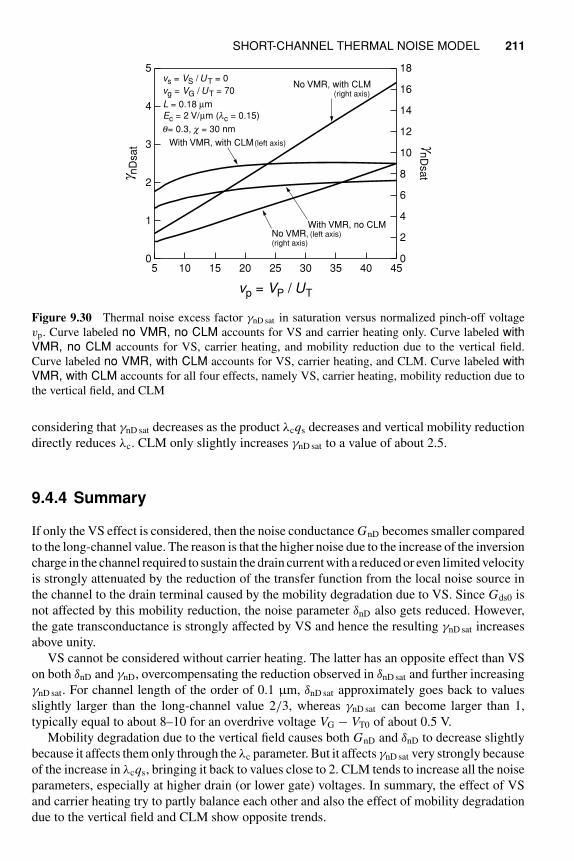
SHORT-CHANNEL THERMAL NOISE MODEL 211
5
4
3
2
1
0
g nD
sat
45403530252015105
vp = VP / UT
18
16
14
12
10
8
6
4
2
0
gnD
sat
No VMR, no CLM(right axis)
With VMR, no CLM (left axis)
With VMR, with CLM (left axis)
No VMR, with CLM(right axis)
vs = VS / UT = 0
vg = VG / UT = 70
L = 0.18 µm
Ec = 2 V/µm (lc = 0.15)
q= 0.3, c = 30 nm
Figure 9.30 Thermal noise excess factor γnD sat in saturation versus normalized pinch-off voltage
vp. Curve labeled no VMR, no CLM accounts for VS and carrier heating only. Curve labeled withVMR, no CLM accounts for VS, carrier heating, and mobility reduction due to the vertical field.
Curve labeled no VMR, with CLM accounts for VS, carrier heating, and CLM. Curve labeled withVMR, with CLM accounts for all four effects, namely VS, carrier heating, mobility reduction due to
the vertical field, and CLM
considering that γnD sat decreases as the product λcqs decreases and vertical mobility reduction
directly reduces λc. CLM only slightly increases γnD sat to a value of about 2.5.
9.4.4 Summary
If only the VS effect is considered, then the noise conductance GnD becomes smaller compared
to the long-channel value. The reason is that the higher noise due to the increase of the inversion
charge in the channel required to sustain the drain current with a reduced or even limited velocity
is strongly attenuated by the reduction of the transfer function from the local noise source in
the channel to the drain terminal caused by the mobility degradation due to VS. Since Gds0 is
not affected by this mobility reduction, the noise parameter δnD also gets reduced. However,
the gate transconductance is strongly affected by VS and hence the resulting γnD sat increases
above unity.
VS cannot be considered without carrier heating. The latter has an opposite effect than VS
on both δnD and γnD, overcompensating the reduction observed in δnD sat and further increasing
γnD sat. For channel length of the order of 0.1 μm, δnD sat approximately goes back to values
slightly larger than the long-channel value 2/3, whereas γnD sat can become larger than 1,
typically equal to about 8–10 for an overdrive voltage VG − VT0 of about 0.5 V.
Mobility degradation due to the vertical field causes both GnD and δnD to decrease slightly
because it affects them only through the λc parameter. But it affects γnD sat very strongly because
of the increase in λcqs, bringing it back to values close to 2. CLM tends to increase all the noise
parameters, especially at higher drain (or lower gate) voltages. In summary, the effect of VS
and carrier heating try to partly balance each other and also the effect of mobility degradation
due to the vertical field and CLM show opposite trends.
212 SHORT-CHANNEL EFFECTS
We can conclude from the above discussion that because of the presence of counteracting
effects, it was possible in the past to present compact thermal noise models without accounting
for all the effects simultaneously and accurately. As the above factors affect γnD and δnD
differently, it is therefore very important to distinguish between the thermal noise parameter
δnD and the thermal noise excess factor γnD. This careful definition of δnD and γnD might
eventually explain the discrepancies observed between values measured by Scholten [130] and
Abidi [131].
10 The Extrinsic Model
The previous chapters were exclusively devoted to the analysis of the intrinsic part of the
transistor, defined as the region comprised between the oxide and substrate on top and bottom,
and the source and drain junctions on each side. Although the fundamental behavior is indeed
dictated by the intrinsic part, the extrinsic part also plays an increasingly important role when
either reducing the dimensions and/or increasing the operating frequency. This chapter looks at
the different components that constitute this extrinsic part. It starts with the access resistances,
which include the source and drain resistances as well as the gate and bulk resistances. They
are all presented in Section 10.2. The regions beyond each end of the intrinsic channel include
the important overlap capacitances and part of the source and drain access resistances. They
are discussed in Section 10.3 with a particular emphasis on their bias dependence. The source
and drain junctions are presented in Section 10.4. Finally, Section 10.5 presents the additional
noise due to the extrinsic components.
10.1 EXTRINSIC PART OF THE DEVICE
Most of the previous chapters were focused on the so-called intrinsic part of the MOS transistor.
It is defined by the inside part of the dashed rectangle shown in Figure 10.1 delimited by the
source and drain junctions on each side, by the gate oxide and gate electrode on the top
and by the substrate on the bottom. This is obviously the most important part of the MOS
transistor, since it represents the active part of the device offering the transconductance and
enabling amplification. To access the source and drain intrinsic terminals (nodes si and di in
Figure 10.1(a)) requires the source and drain extensions (SDE), as well as the source and drain
diffusions which are covered with a silicide and contacted by a via. All these parts add some
parasitic access resistances which are modeled by the source and drain resistances RS and RD.
The latter are made of several parts that will be further discussed in Section 10.2.1. The gate is
made of polysilicon which is usually covered by silicide in order to lower the gate resistance.
Although this resistance is small (in the order of a few /), it might be important to account
for it particularly for RF I C design, where even small series resistances can count. The access
to the gate can also be modeled by a simple gate resistance RG. The modeling of the substrate
Charge-Based MOS Transistor Modeling: The EKV Model for Low-Power and RF IC Design C. Enz and E. VittozC© 2006 John Wiley & Sons, Ltd.
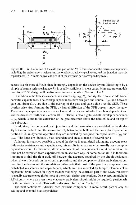
214 THE EXTRINSIC MODEL
bi
G
B
S D
RGCGDoCGBo
DDDS
CGSo
RB
RDRS
si Intrinsic part di
gi
RB
RG
RDRS
CGDo CGBoCGSo
G
S D
B
gi
bi
disi
Intrinsic part of the transistor
DS DD
(a) (b)
Figure 10.1 (a) Definition of the extrinsic part of the MOS transistor and the extrinsic components
including the series access resistances, the overlap parasitic capacitances, and the junction parasitic
capacitances. (b) Simple equivalent circuit of the extrinsic part corresponding to (a)
access is a bit more difficult since it strongly depends on the device layout. Modeling it by a
simple substrate series resistance RB is usually sufficient in most cases. More accurate models
used for RF I C design will be discussed in more details in Section 11.4.2.
In addition to the four series access resistances RS, RD, RG, and RB, there are also additional
parasitic capacitances. The overlap capacitances between gate and source CGSo and between
gate and drain CGDo are due to the overlap of the gate and gate oxide over the SDE. These
overlap arise after forming the SDE, by lateral diffusion of the SDE dopants under the gate.
These overlap capacitances are made of several parts some of which are bias dependent and
will be discussed further in Section 10.3.1. There is also a gate-to-bulk overlap capacitance
CGBo which is due to the extension of the gate electrode above the field oxide and on top of
the substrate.
In addition, the source and drain junctions and their extensions are modeled by the diodes
DS between the bulk and the source and DD between the bulk and the drain. As explained in
Section 10.4, in dynamic operation they are modeled by two junction capacitances CBSj and
CBDj. The latter are obviously bias dependent and are also made of several parts.
Although it is always possible to model the device in great detail taking into account every
little series resistances and capacitances, this results in an accurate but usually very complex
equivalent circuit. Furthermore, all the components of this equivalent circuit can most of the
time not be extracted from experiments in an accurate way, or some not at all. It is therefore
important to find the right trade-off between the accuracy required by the circuit designers,
which always depends on the circuit application, and the complexity of the equivalent circuit
used for the design and the simulations. Also note that most of the parasitic components are
distributed resistances and capacitances, which are then modeled by lumped elements. The
equivalent circuit shown in Figure 10.1(b) modeling the extrinsic part of the MOS transistor
is usually accurate enough for most of the circuit design applications. One exception might be
RF circuits, where an even more elaborate equivalent circuit might be required, particularly
for the substrate network. This will be discussed further in Chapter 11.
The next sections will discuss each extrinsic component in more detail, particularly its
scaling and eventual bias dependence.
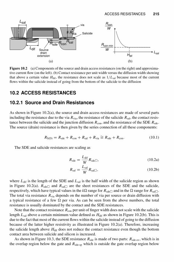
ACCESS RESISTANCES 215
Ldif
Lsal
RconRsal
Rvia
via
Salicide
Sourcedrain
extension
Rsde
LsalHdif
Rcon
W
Rcon-min
W
(a) (b)
Figure 10.2 (a) Components of the source and drain access resistances (on the right) and approxima-
tive current flow (on the left). (b) Contact resistance per unit width versus the diffusion width showing
that above a certain value Hdif, the resistance does not scale as 1/Lsal because most of the current
flows within the salicide instead of going from the bottom of the salicide to the diffusion
10.2 ACCESS RESISTANCES
10.2.1 Source and Drain Resistances
As shown in Figure 10.2(a), the source and drain access resistances are made of several parts
including the resistance due to the via Rvia, the resistance of the salicide Rsal, the contact resis-
tance between the salicide and the junction diffusion Rcon, and the resistance of the SDE Rsde.
The source (drain) resistance is then given by the series connection of all these components:
RS(D) = Rsde + Rcon + Rsal + Rvia∼= Rsde + Rcon. (10.1)
The SDE and salicide resistances are scaling as
Rsde =Ldif
WRsde, (10.2a)
Rsal =Lsal
WRsal, (10.2b)
where Ldif is the length of the SDE and Lsal is the half width of the salicide region as shown
in Figure 10.2(a). Rsde and Rsal are the sheet resistances of the SDE and the salicide,
respectively, which have typical values in the k range for Rsde and in the range for Rsal.
The total via resistance Rvia depends on the number of via per source or drain diffusion with
a typical resistance of a few per via. As can be seen from the above numbers, the total
resistance is usually dominated by the contact and the SDE resistances.
Note that the contact resistance Rcon per unit of finger width does not scale with the salicide
length Lsal above a certain minimum value defined as Hdif as shown in Figure 10.2(b). This is
due to the fact that most of the current flows within the salicide instead of going to the diffusion
because of the latter higher resistivity as illustrated in Figure 10.2(a). Therefore, increasing
the salicide length above Hdif does not reduce the contact resistance even though the bottom
contact area between salicide and silicon is increased.
As shown in Figure 10.3, the SDE resistance Rsde is made of two parts: Rsde-ov, which is in
the overlap region below the gate and Rsde-sp which is outside the gate overlap region below
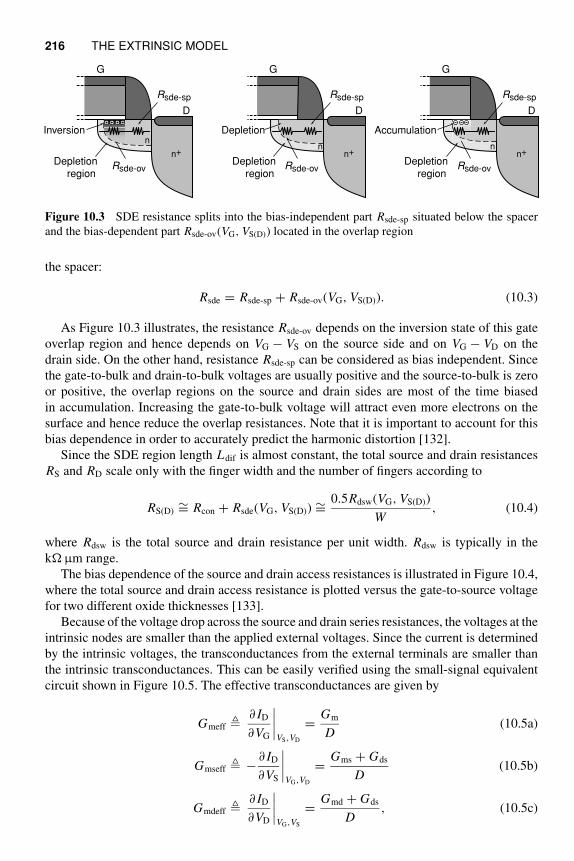
216 THE EXTRINSIC MODEL
Depletionregion
Depletion
G
D
nn+
Rsde-ov
Rsde-sp
Depletionregion
Accumulation
G
D
nn+
Rsde-ov
Rsde-sp
Depletionregion
Inversion
G
D
n
n+
Rsde-ov
Rsde-sp
Figure 10.3 SDE resistance splits into the bias-independent part Rsde-sp situated below the spacer
and the bias-dependent part Rsde-ov(VG, VS(D)) located in the overlap region
the spacer:
Rsde = Rsde-sp + Rsde-ov(VG, VS(D)). (10.3)
As Figure 10.3 illustrates, the resistance Rsde-ov depends on the inversion state of this gate
overlap region and hence depends on VG − VS on the source side and on VG − VD on the
drain side. On the other hand, resistance Rsde-sp can be considered as bias independent. Since
the gate-to-bulk and drain-to-bulk voltages are usually positive and the source-to-bulk is zero
or positive, the overlap regions on the source and drain sides are most of the time biased
in accumulation. Increasing the gate-to-bulk voltage will attract even more electrons on the
surface and hence reduce the overlap resistances. Note that it is important to account for this
bias dependence in order to accurately predict the harmonic distortion [132].
Since the SDE region length Ldif is almost constant, the total source and drain resistances
RS and RD scale only with the finger width and the number of fingers according to
RS(D)∼= Rcon + Rsde(VG, VS(D)) ∼=
0.5Rdsw(VG, VS(D))
W, (10.4)
where Rdsw is the total source and drain resistance per unit width. Rdsw is typically in the
k μm range.
The bias dependence of the source and drain access resistances is illustrated in Figure 10.4,
where the total source and drain access resistance is plotted versus the gate-to-source voltage
for two different oxide thicknesses [133].
Because of the voltage drop across the source and drain series resistances, the voltages at the
intrinsic nodes are smaller than the applied external voltages. Since the current is determined
by the intrinsic voltages, the transconductances from the external terminals are smaller than
the intrinsic transconductances. This can be easily verified using the small-signal equivalent
circuit shown in Figure 10.5. The effective transconductances are given by
Gmeff ∂ ID
∂VG
∣∣∣∣
VS,VD
=Gm
D(10.5a)
Gmseff −∂ ID
∂VS
∣∣∣∣
VG,VD
=Gms + Gds
D(10.5b)
Gmdeff ∂ ID
∂VD
∣∣∣∣
VG,VS
=Gmd + Gds
D, (10.5c)
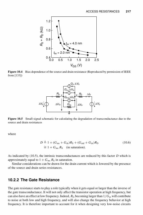
ACCESS RESISTANCES 217
tox = 4.0 nm
tox = 2.0 nm
1.2
1.0
0.8
0.6
0.40.0 0.5 1.0
VGS (V)
1.5 2.0 2.5
RS +
RD (
kΩ
)
Figure 10.4 Bias dependence of the source and drain resistance (Reproduced by permission of IEEE
from [133])
Gm ∆VG
Gms ∆VSi
Gmd ∆VDi
Gds
RS RD
∆VD∆VS
disi
∆VSi ∆VDi
∆ID
Figure 10.5 Small-signal schematic for calculating the degradation of transconductance due to the
source and drain resistances
where
D 1 + (Gms + Gds)RS + (Gmd + Gds)RD (10.6)
∼= 1 + Gms RS (in saturation).
As indicated by (10.5), the intrinsic transconductances are reduced by this factor D which is
approximately equal to 1 + Gms RS in saturation.
Similar considerations can be drawn for the drain current which is lowered by the presence
of the source and drain series resistances.
10.2.2 The Gate Resistance
The gate resistance starts to play a role typically when it gets equal or larger than the inverse of
the gate transconductance. It will not only affect the transistor operation at high frequency, but
can also have an effect at low frequency. Indeed, RG becoming larger than 1/Gm will contribute
to noise at both low and high frequency, and will also change the frequency behavior at high
frequency. It is therefore important to account for it when designing very low-noise circuits
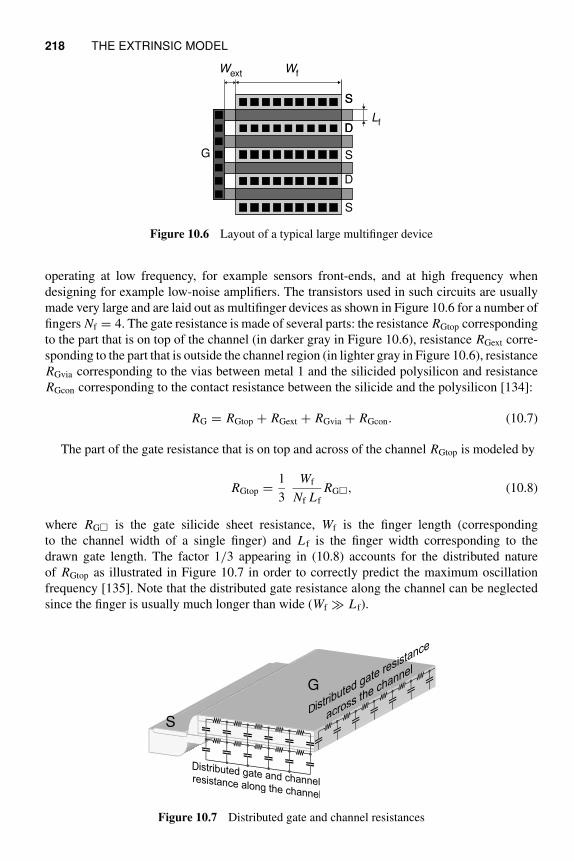
218 THE EXTRINSIC MODEL
G
S
D
S
D
WfWext
S
D
S
Lf
Figure 10.6 Layout of a typical large multifinger device
operating at low frequency, for example sensors front-ends, and at high frequency when
designing for example low-noise amplifiers. The transistors used in such circuits are usually
made very large and are laid out as multifinger devices as shown in Figure 10.6 for a number of
fingers Nf = 4. The gate resistance is made of several parts: the resistance RGtop corresponding
to the part that is on top of the channel (in darker gray in Figure 10.6), resistance RGext corre-
sponding to the part that is outside the channel region (in lighter gray in Figure 10.6), resistance
RGvia corresponding to the vias between metal 1 and the silicided polysilicon and resistance
RGcon corresponding to the contact resistance between the silicide and the polysilicon [134]:
RG = RGtop + RGext + RGvia + RGcon. (10.7)
The part of the gate resistance that is on top and across of the channel RGtop is modeled by
RGtop =1
3
Wf
Nf L f
RG, (10.8)
where RG is the gate silicide sheet resistance, Wf is the finger length (corresponding
to the channel width of a single finger) and L f is the finger width corresponding to the
drawn gate length. The factor 1/3 appearing in (10.8) accounts for the distributed nature
of RGtop as illustrated in Figure 10.7 in order to correctly predict the maximum oscillation
frequency [135]. Note that the distributed gate resistance along the channel can be neglected
since the finger is usually much longer than wide (Wf ≫ L f).
G
S
D
D
Figure 10.7 Distributed gate and channel resistances
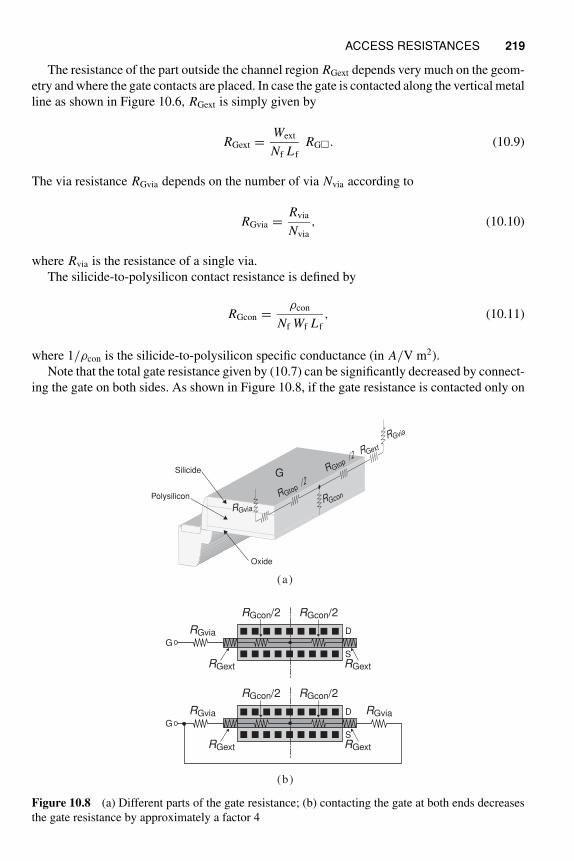
ACCESS RESISTANCES 219
The resistance of the part outside the channel region RGext depends very much on the geom-
etry and where the gate contacts are placed. In case the gate is contacted along the vertical metal
line as shown in Figure 10.6, RGext is simply given by
RGext =Wext
Nf L f
RG. (10.9)
The via resistance RGvia depends on the number of via Nvia according to
RGvia =Rvia
Nvia
, (10.10)
where Rvia is the resistance of a single via.
The silicide-to-polysilicon contact resistance is defined by
RGcon =ρcon
Nf Wf L f
, (10.11)
where 1/ρcon is the silicide-to-polysilicon specific conductance (in A/V m2).
Note that the total gate resistance given by (10.7) can be significantly decreased by connect-
ing the gate on both sides. As shown in Figure 10.8, if the gate resistance is contacted only on
G
Polysilicon
Oxide
Silicide
G
D
S
RGvia
RGext RGext
RGcon/2 RGcon/2
G
D
S
RGvia RGvia
RGext RGext
RGcon/2 RGcon/2
(a)
(b)
RGtop
RGtop
RGvia
RGext
RGcon
RGvia
Figure 10.8 (a) Different parts of the gate resistance; (b) contacting the gate at both ends decreases
the gate resistance by approximately a factor 4
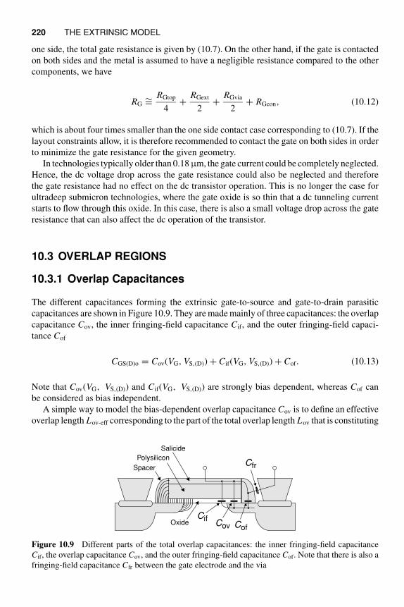
220 THE EXTRINSIC MODEL
one side, the total gate resistance is given by (10.7). On the other hand, if the gate is contacted
on both sides and the metal is assumed to have a negligible resistance compared to the other
components, we have
RG∼=
RGtop
4+
RGext
2+
RGvia
2+ RGcon, (10.12)
which is about four times smaller than the one side contact case corresponding to (10.7). If the
layout constraints allow, it is therefore recommended to contact the gate on both sides in order
to minimize the gate resistance for the given geometry.
In technologies typically older than 0.18 μm, the gate current could be completely neglected.
Hence, the dc voltage drop across the gate resistance could also be neglected and therefore
the gate resistance had no effect on the dc transistor operation. This is no longer the case for
ultradeep submicron technologies, where the gate oxide is so thin that a dc tunneling current
starts to flow through this oxide. In this case, there is also a small voltage drop across the gate
resistance that can also affect the dc operation of the transistor.
10.3 OVERLAP REGIONS
10.3.1 Overlap Capacitances
The different capacitances forming the extrinsic gate-to-source and gate-to-drain parasitic
capacitances are shown in Figure 10.9. They are made mainly of three capacitances: the overlap
capacitance Cov, the inner fringing-field capacitance Cif, and the outer fringing-field capaci-
tance Cof
CGS(D)o = Cov(VG, VS,(D)) + Cif(VG, VS,(D)) + Cof. (10.13)
Note that Cov(VG, VS,(D)) and Cif(VG, VS,(D)) are strongly bias dependent, whereas Cof can
be considered as bias independent.
A simple way to model the bias-dependent overlap capacitance Cov is to define an effective
overlap length Lov-eff corresponding to the part of the total overlap length Lov that is constituting
Cov Cof
Cif
Cfr
Salicide
Polysilicon
Spacer
Oxide
Figure 10.9 Different parts of the total overlap capacitances: the inner fringing-field capacitance
Cif, the overlap capacitance Cov, and the outer fringing-field capacitance Cof. Note that there is also a
fringing-field capacitance Cfr between the gate electrode and the via
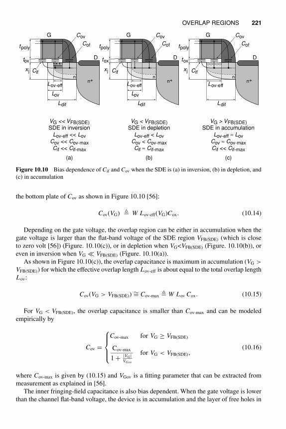
OVERLAP REGIONS 221
VG << VFB(SDE)SDE in inversion
Lov-eff << LovCov << Cov-maxCif << Cif-max
(a)
G
D
nn+
Cof
Cov
Lov-eff
Lov
Ldif
Cif
tpoly
tox
xj
VG < VFB(SDE)SDE in depletion
Lov-eff < LovCov < Cov-maxCif ≈ Cif-max
(b)
G
D
nn+
Lov-eff
Lov
Ldif
Cof
Cov
Cif
tpoly
tox
x j
VG > VFB(SDE)SDE in accumulation
Lov-eff ≈ LovCov ≈ Cov-maxCif << Cif-max
(c)
Ldif
G
D
nn+
Cof
Cov
Lov-eff
Cif
tpoly
tox
xj
Figure 10.10 Bias dependence of Cif and Cov when the SDE is (a) in inversion, (b) in depletion, and
(c) in accumulation
the bottom plate of Cov as shown in Figure 10.10 [56]:
Cov(VG) W Lov-eff(VG)Cox. (10.14)
Depending on the gate voltage, the overlap region can be either in accumulation when the
gate voltage is larger than the flat-band voltage of the SDE region VFB(SDE) (which is close
to zero volt [56]) (Figure. 10.10(c)), or in depletion when VG<VFB(SDE) (Figure. 10.10(b)), or
even in inversion when VG ≪ VFB(SDE) (Figure. 10.10(a)).
As shown in Figure 10.10(c)), the overlap capacitance is maximum in accumulation (VG >
VFB(SDE)) for which the effective overlap length Lov-eff is about equal to the total overlap length
Lov:
Cov(VG > VFB(SDE)) ∼= Cov-max W Lov Cox. (10.15)
For VG < VFB(SDE), the overlap capacitance is smaller than Cov-max and can be modeled
empirically by
Cov =
⎧
⎪
⎪
⎨
⎪
⎪
⎩
Cov-max for VG ≥ VFB(SDE)
Cov-max
1 +|VG |
VGov
for VG < VFB(SDE),(10.16)
where Cov-max is given by (10.15) and VGov is a fitting parameter that can be extracted from
measurement as explained in [56].
The inner fringing-field capacitance is also bias dependent. When the gate voltage is lower
than the channel flat-band voltage, the device is in accumulation and the layer of free holes in
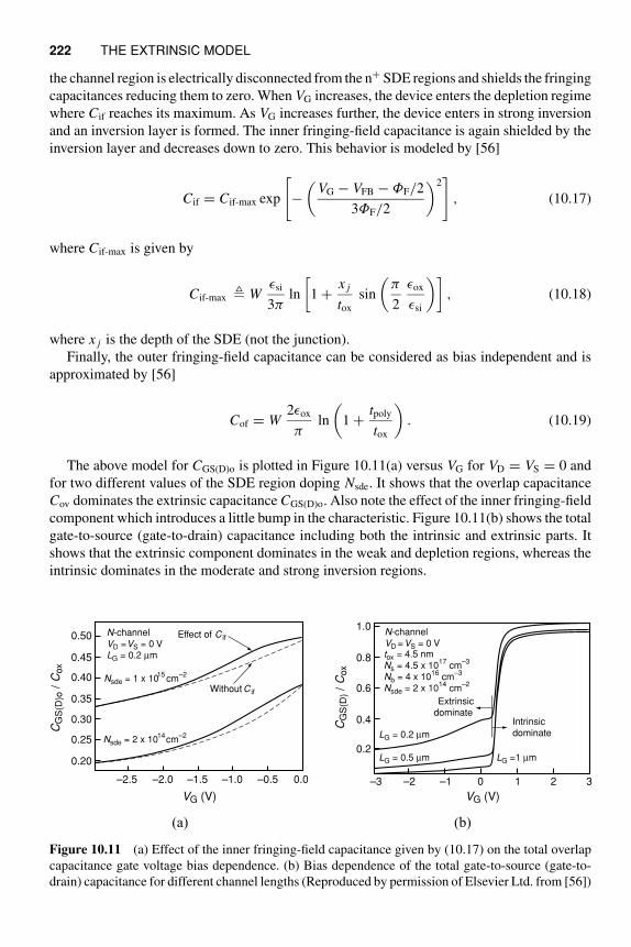
222 THE EXTRINSIC MODEL
the channel region is electrically disconnected from the n+ SDE regions and shields the fringing
capacitances reducing them to zero. When VG increases, the device enters the depletion regime
where Cif reaches its maximum. As VG increases further, the device enters in strong inversion
and an inversion layer is formed. The inner fringing-field capacitance is again shielded by the
inversion layer and decreases down to zero. This behavior is modeled by [56]
Cif = Cif-max exp
[
−(
VG − VFB − ΦF/2
3ΦF/2
)2]
, (10.17)
where Cif-max is given by
Cif-max Wǫsi
3πln
[
1 +x j
tox
sin
(
π
2
ǫox
ǫsi
)]
, (10.18)
where x j is the depth of the SDE (not the junction).
Finally, the outer fringing-field capacitance can be considered as bias independent and is
approximated by [56]
Cof = W2ǫox
πln
(
1 +tpoly
tox
)
. (10.19)
The above model for CGS(D)o is plotted in Figure 10.11(a) versus VG for VD = VS = 0 and
for two different values of the SDE region doping Nsde. It shows that the overlap capacitance
Cov dominates the extrinsic capacitance CGS(D)o. Also note the effect of the inner fringing-field
component which introduces a little bump in the characteristic. Figure 10.11(b) shows the total
gate-to-source (gate-to-drain) capacitance including both the intrinsic and extrinsic parts. It
shows that the extrinsic component dominates in the weak and depletion regions, whereas the
intrinsic dominates in the moderate and strong inversion regions.
–3 –2 –1 0 1 2 3
1.0
0.8
0.6
0.4
0.2
VG (V)
CG
S(D
) / C
ox
LG = 0.2 µm
LG = 0.5 µm LG =1 µm
N-channelVD =VS = 0 V
Extrinsicdominate
Intrinsicdominate
tox = 4.5 nmNs = 4.5 x 10
17 cm
–3
Nb = 4 x 10¹⁶
cm–3
Nsde = 2 x 10¹⁴
cm–2
–2.5
0.50
0.45
0.40
0.35
0.30
0.25
0.20
–2.0 –1.5 –1.0 –0.5 0.0
VG (V)
CG
S(D
)o / C
ox
Nsde = 2 x 10¹⁴
cm–2
Nsde = 1 x 10¹⁵
cm–2
N-channelVD = VS = 0 VLG = 0.2 µm
Effect of C if
Without C if
(a) (b)
Figure 10.11 (a) Effect of the inner fringing-field capacitance given by (10.17) on the total overlap
capacitance gate voltage bias dependence. (b) Bias dependence of the total gate-to-source (gate-to-
drain) capacitance for different channel lengths (Reproduced by permission of Elsevier Ltd. from [56])
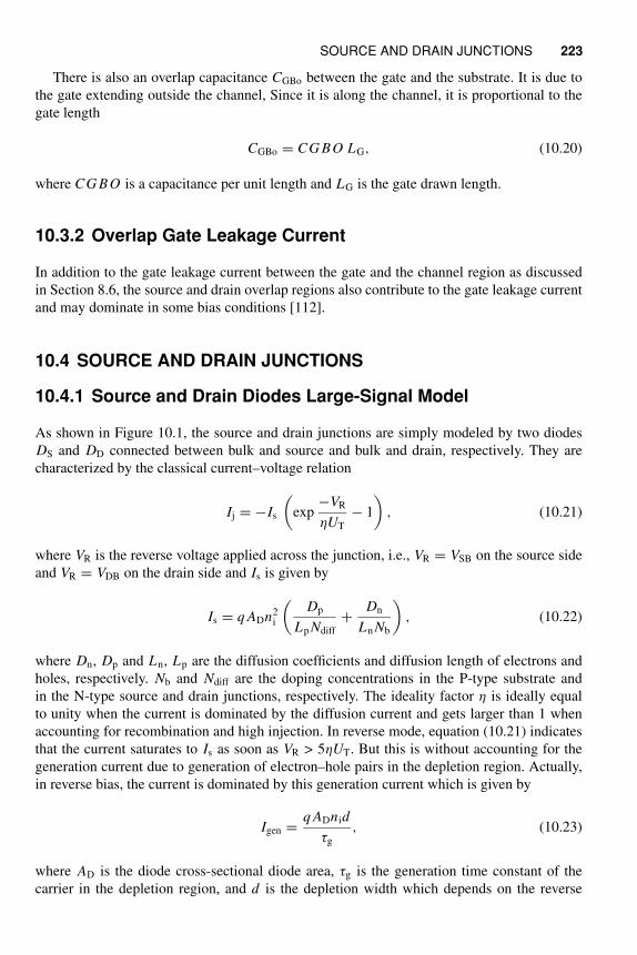
SOURCE AND DRAIN JUNCTIONS 223
There is also an overlap capacitance CGBo between the gate and the substrate. It is due to
the gate extending outside the channel, Since it is along the channel, it is proportional to the
gate length
CGBo = CG BO LG, (10.20)
where CG BO is a capacitance per unit length and LG is the gate drawn length.
10.3.2 Overlap Gate Leakage Current
In addition to the gate leakage current between the gate and the channel region as discussed
in Section 8.6, the source and drain overlap regions also contribute to the gate leakage current
and may dominate in some bias conditions [112].
10.4 SOURCE AND DRAIN JUNCTIONS
10.4.1 Source and Drain Diodes Large-Signal Model
As shown in Figure 10.1, the source and drain junctions are simply modeled by two diodes
DS and DD connected between bulk and source and bulk and drain, respectively. They are
characterized by the classical current–voltage relation
Ij = −Is
(
exp−VR
ηUT
− 1
)
, (10.21)
where VR is the reverse voltage applied across the junction, i.e., VR = VSB on the source side
and VR = VDB on the drain side and Is is given by
Is = q ADn2i
(
Dp
Lp Ndiff
+Dn
Ln Nb
)
, (10.22)
where Dn, Dp and Ln, Lp are the diffusion coefficients and diffusion length of electrons and
holes, respectively. Nb and Ndiff are the doping concentrations in the P-type substrate and
in the N-type source and drain junctions, respectively. The ideality factor η is ideally equal
to unity when the current is dominated by the diffusion current and gets larger than 1 when
accounting for recombination and high injection. In reverse mode, equation (10.21) indicates
that the current saturates to Is as soon as VR > 5ηUT. But this is without accounting for the
generation current due to generation of electron–hole pairs in the depletion region. Actually,
in reverse bias, the current is dominated by this generation current which is given by
Igen =q ADnid
τg
, (10.23)
where AD is the diode cross-sectional diode area, τg is the generation time constant of the
carrier in the depletion region, and d is the depletion width which depends on the reverse
224 THE EXTRINSIC MODEL
voltage VR according to
d =
√
2ǫsi
q
Nb + Ndiff
Nb Ndiff
√
VR + ΦB, (10.24)
where ΦB is the built-in potential
ΦB = UT lnNb Ndiff
n2i
. (10.25)
In most cases the junctions are N+-P type with Ndiff ≫ Nb and (10.24) simplifies to
d ∼=
√
2ǫsi
q Nb
√
VR + ΦB. (10.26)
The current flowing in the reverse-biased source (drain) junction is then given by
IS(D)B∼= Is + Igen (10.27)
and depends on the bias voltages mainly through the generation current Igen.
If the reverse bias voltage is increased further, so does the electric field in the depletion
region until it reaches a critical value Ejc corresponding to the avalanche breakdown voltage
Vbr
Vbr =ǫsi E
2jc
2q
(
1
Nb
+1
Ndiff.
)
. (10.28)
Equation (10.28) shows that the breakdown voltage decreases when increasing the doping on
either side of the junction. As shown in Figure 10.12(a), as soon as VR gets slightly larger than
Vbr, the reverse current starts to increase sharply.
The small-signal equivalent circuit of the diodes is shown in Figure 10.12(c), where the
junction capacitances are described in Section 10.4.2 and the differential conductances in
Section 10.4.3.
10.4.2 Source and Drain Junction Capacitances
The source and drain junction capacitances CBSj and CBDj of Figure 10.12(c) model the vari-
ations of the depletion charge due to a change of the depletion width. A junction capacitance
can be simply modeled as a parallel plate capacitor with silicon as dielectric and separated by
a distance d
Cj =ǫsi
d, (10.29)
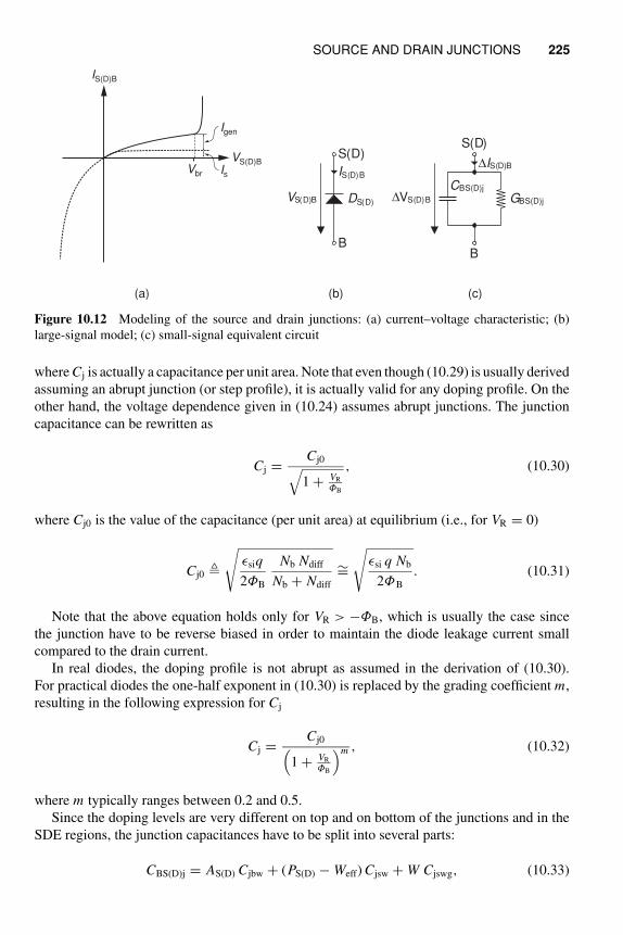
SOURCE AND DRAIN JUNCTIONS 225
DS(D)
S(D)
B
IS(D)B
VS(D)B
(b)
CBS(D)j
GBS(D)j
B
∆IS(D)B
S(D)
∆VS(D)B
(c)(a)
IS(D)B
VS(D)BIs
Igen
Vbr
Figure 10.12 Modeling of the source and drain junctions: (a) current–voltage characteristic; (b)
large-signal model; (c) small-signal equivalent circuit
where Cj is actually a capacitance per unit area. Note that even though (10.29) is usually derived
assuming an abrupt junction (or step profile), it is actually valid for any doping profile. On the
other hand, the voltage dependence given in (10.24) assumes abrupt junctions. The junction
capacitance can be rewritten as
Cj =Cj0
√
1 + VR
ΦB
, (10.30)
where Cj0 is the value of the capacitance (per unit area) at equilibrium (i.e., for VR = 0)
Cj0
√
ǫsiq
2ΦB
Nb Ndiff
Nb + Ndiff
∼=
√
ǫsi q Nb
2ΦB
. (10.31)
Note that the above equation holds only for VR > −ΦB, which is usually the case since
the junction have to be reverse biased in order to maintain the diode leakage current small
compared to the drain current.
In real diodes, the doping profile is not abrupt as assumed in the derivation of (10.30).
For practical diodes the one-half exponent in (10.30) is replaced by the grading coefficient m,
resulting in the following expression for Cj
Cj =Cj0
(
1 + VR
ΦB
)m , (10.32)
where m typically ranges between 0.2 and 0.5.
Since the doping levels are very different on top and on bottom of the junctions and in the
SDE regions, the junction capacitances have to be split into several parts:
CBS(D)j = AS(D) Cjbw + (PS(D) − Weff) Cjsw + W Cjswg, (10.33)
226 THE EXTRINSIC MODEL
where Cjbw refers to the bottom-wall capacitance per unit area, Cjsw to the side-wall capacitance
per unit length of the perimeter that is on the isolated sides, and Cjswg to the side-wall capacitance
per unit length of the part of the perimeter that is along the gate and the SDE region. AS (AD)
is the total source (drain) diffusion area, PS (PD) is the total source (drain) diffusion perimeter,
and W is the total transistor width.
Note that for devices that are inside a well, an additional junction capacitance CBB′j between
the well and the substrate has to be considered. The latter is decomposed into
CBB′j = AW Cjbww + PW Cjsww, (10.34)
where Cjbww refers to the bottom-wall capacitance per unit area and Cjsww to the side-wall
capacitance per unit length of the well. AW corresponds to the total well area, whereas PW is
the total well perimeter.
10.4.3 Source and Drain Junction Conductances
The source and drain junctions small-signal schematic should be completed with two differen-
tial conductances GBSj and GBDj that are connected in parallel with the junction capacitances
as shown in Figure 10.12(c). The conductances are obtained by differentiating the expression
of the leakage current (10.27) resulting in
GBS(D)j =ADni
τg
Nb + Ndiff
Nb Ndiff
Cj∼=
ADni
τg Nb
Cj. (10.35)
These conductances can often be neglected since they are usually much smaller than the
intrinsic (trans)conductances and output conductance Gds. However, they may become non-
negligible at very low channel current, for which the intrinsic (trans)conductances become
very small, or if the effect of Gds has been canceled as is the case in a cascode configuration.
10.5 EXTRINSIC NOISE SOURCES
The different noise sources appearing at low frequency in a MOS transistor are represented
in the small-signal schematic of Figure 10.13.1 The overall noise is usually dominated by the
intrinsic part of the device representing the active part and corresponding in Figure 10.13 to the
noise source InD [114,134]. It comprises both the flicker and thermal noise due to the channel,
which were already presented in Sections 6.2 and 6.3. In addition, all the access resistances,
namely the source and drain resistances RS and RD but also the gate and the substrate resistances
RG and RB are also noisy and contribute to the thermal and to some extend also to the flicker
noise (see Section 6.3.3). They are represented in Figure 10.13 by the noise current sources
InRS, InRD, InRG, and InRB respectively. If their contributions to the flicker noise is neglected,
1 This small-signal equivalent circuit does not include the noise appearing at high frequency. The latter are discussed
in Chapter 13.
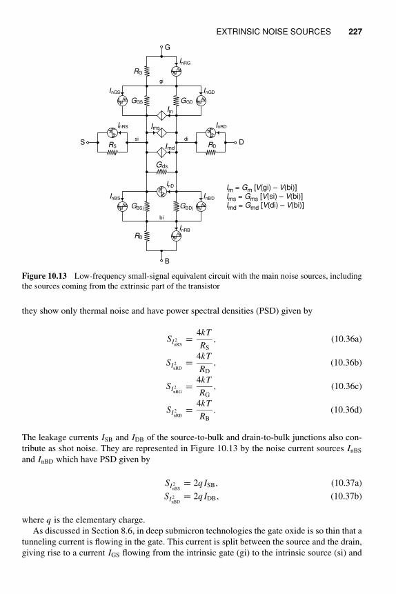
EXTRINSIC NOISE SOURCES 227
Im = Gm [V(gi) – V(bi)]Ims = Gms [V(si) – V(bi)]Imd = Gmd [V(di) – V(bi)]
Im
Ims
Imd
Gds
InRS
RS
GBSj GBDj
InD
RB
InBS
InRB
InBD
GGS GGD
InGS InGD
RG
InRG
InRD
RD
si di
gi
bi
G
B
DS
Figure 10.13 Low-frequency small-signal equivalent circuit with the main noise sources, including
the sources coming from the extrinsic part of the transistor
they show only thermal noise and have power spectral densities (PSD) given by
SI 2nRS
=4kT
RS
, (10.36a)
SI 2nRD
=4kT
RD
, (10.36b)
SI 2nRG
=4kT
RG
, (10.36c)
SI 2nRB
=4kT
RB
. (10.36d)
The leakage currents ISB and IDB of the source-to-bulk and drain-to-bulk junctions also con-
tribute as shot noise. They are represented in Figure 10.13 by the noise current sources InBS
and InBD which have PSD given by
SI 2nBS
= 2q ISB, (10.37a)
SI 2nBD
= 2q IDB, (10.37b)
where q is the elementary charge.
As discussed in Section 8.6, in deep submicron technologies the gate oxide is so thin that a
tunneling current is flowing in the gate. This current is split between the source and the drain,
giving rise to a current IGS flowing from the intrinsic gate (gi) to the intrinsic source (si) and
228 THE EXTRINSIC MODEL
another current IGD flowing from the intrinsic gate (gi) to the intrinsic drain (di). Both of these
currents show shot noise. They are represented in Figure 10.13 by the noise current sources
InGS and InGD having PSD
SI 2nGS
= 2q IGS, (10.38a)
SI 2nG D
= 2q IGD. (10.38b)
The conductances GGS and GGD in Figure 10.13 represent the small-signal differential con-
ductances corresponding to these leakage currents.
Part III
The High-Frequency Model
The aggressive scaling of CMOS technologies which is going on since more than 25 years has
allowed to increase the number of transistors per chips and hence extend the functionality and
in the same time dramatically push the speed performance. Although these tremendous speed
improvements have been mainly driven by the requirements of VLSI digital chips, they can
also be exploited for analog RF circuits. Today, ultradeep submicron (UDSM) technologies
have catched-up or even surpassed the transit frequencies achieved by bipolar transistors. This
clearly opens the door to full CMOS highly integrated solutions for wireless applications.
After several years of intensive research that has demonstrated the feasibility of using CMOS
technologies for RF applications, real products using CMOS also for the RF portion of a chip
are now emerging. Several examples of single-chip systems, including the radio transceiver
together with the baseband digital processor and fully integrated in CMOS, are on the market
today. Nevertheless, the design of RF I Cs for real products remains a challenge due to the strong
constraints on power consumption and noise that leave little margins for the RF I C designer. It is
therefore crucial to be able to accurately predict the performance of CMOS RF circuits in order
to improve design efficiency and reduce time-to-market. This requires MOS transistor models
that are accurate over a wide range of bias, from dc to RF and for a large set of geometries.
Part III presents an overview of the high-frequency aspects of MOS transistor modeling for
RF I C design. Chapter 11 presents the equivalent circuit at RF, whereas Chapter 12 focuses
on the small-signal circuit. RF thermal noise is finally presented in Chapter 13.
Charge-Based MOS Transistor Modeling: The EKV Model for Low-Power and RF IC Design C. Enz and E. VittozC© 2006 John Wiley & Sons, Ltd.

11 Equivalent Circuit at RF
This chapter first presents the structure and layout of a typical RF MOS transistor. It then
briefly looks at what is really changing when moving to higher frequency. Several figures
of merit widely used to evaluate and compare different devices and technologies are defined
in Section 11.3. They include the transit frequency, the maximum frequency of oscillation,
and the minimum noise figure. Section 11.3.4 points out that the moderate inversion offers a
good trade-off between the power consumption, the low-voltage operation, the noise, and the
linearity, all being of major importance for designing RF circuits. Section 11.4 then presents
the equivalent large-signal circuit valid at RF. It highlights the importance of a correct modeling
of the substrate.
11.1 RF MOS TRANSISTOR STRUCTURE AND LAYOUT
RF MOS transistors are usually designed as large devices in order to achieve the desired
transconductance required to meet the RF requirements. As shown in Figure 11.1, they are
usually laid out as multifinger devices, because in deep submicron CMOS processes, the
maximum finger length (corresponding to the unit transistor width Wf) is limited. This is
due to the so-called “narrow-line effect” increasing the silicided polysilicon sheet resistance
as the finger width (corresponding to the transistor gate length L f) decreases due to grain
boundary problems [136]. Typical devices have up to 10 or more fingers. The total transistor
effective width is then simply W = NfWf.
11.2 WHAT CHANGES AT RF?
When increasing the operating frequency for a given transistor, the characteristics such as the
gain or the transconductance (or more precisely the transadmittance) start to degrade. The
sources of this degradation must be distinguished between those coming from the intrinsic part
of the device (the channel region) and those related to the extrinsic part of the transistor (i.e.,
all the parasitic components discussed in Chapter 10). The frequency limit of the intrinsic part
Charge-Based MOS Transistor Modeling: The EKV Model for Low-Power and RF IC Design C. Enz and E. VittozC© 2006 John Wiley & Sons, Ltd.
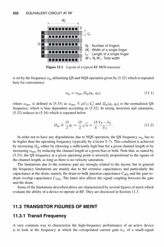
232 EQUIVALENT CIRCUIT AT RF
G
S
D
S
D
Wf
S
Lf
Nf : Number of fingersWf : Width of a single fingerLf : Length of a single fingerW = Nf W f: Total width
Figure 11.1 Layout of a typical RF MOS transistor
is set by the frequency ωqs delimiting QS and NQS operation given by (5.32) which is repeated
here for convenience
ωqs = ωspec Ωqs(qs, qd), (11.1)
where ωspec is defined in (5.33) as ωspec µUT/L2f and Ωqs(qs, qd) is the normalized QS
frequency, which is bias dependent according to (5.32). In strong inversion and saturation,
(5.32) reduces to (5.34) which is repeated below
Ωqs∼=
15
2qs =
15
2
√
if =15
4
VP − VS
UT
. (11.2)
In order not to have any degradations due to NQS operation, the QS frequency ωqs has to
be higher than the operating frequency (typically by a factor 5–7). This condition is achieved
by increasing Ωqs either by choosing a sufficiently high bias for a given channel length or by
increasing ωspec by reducing the channel length at a given bias or both. Note that, as stated by
(5.33), the QS frequency at a given operating point is inversely proportional to the square of
the channel length, as long as there is no velocity saturation.
The limitations due to the extrinsic part are strongly related to the layout, but in general
the frequency limitations are mainly due to the extrinsic capacitances and particularly the
capacitance at the drain, namely the drain-to-bulk junction capacitance CBDj and the gate-to-
drain overlap capacitance CGDo. The latter also affects the signal coupling between the gate
and the drain.
Some of the limitations described above are characterized by several figures of merit which
evaluate the ability of a device to operate at RF. They are discussed in Section 11.3.
11.3 TRANSISTOR FIGURES OF MERIT
11.3.1 Transit Frequency
A very common way to characterize the high-frequency performance of an active device
is to look at the frequency at which the extrapolated current gain h21 of a small-signal
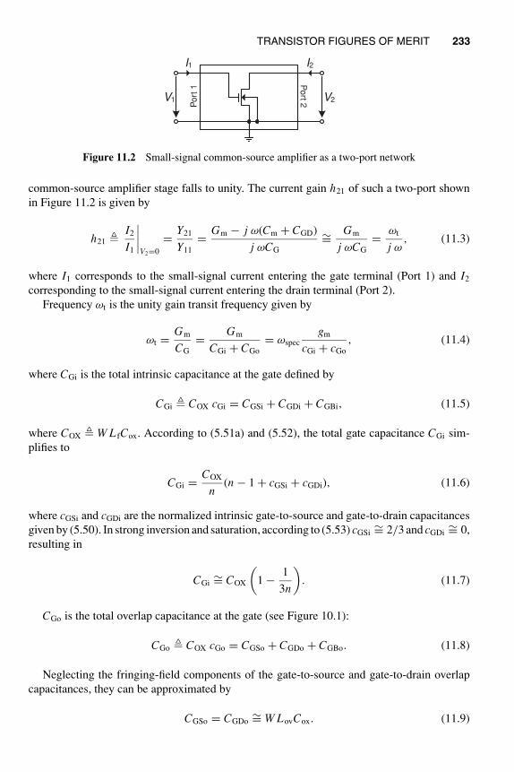
TRANSISTOR FIGURES OF MERIT 233
I1 I2
V1 V2
Port
1
Port 2
Figure 11.2 Small-signal common-source amplifier as a two-port network
common-source amplifier stage falls to unity. The current gain h21 of such a two-port shown
in Figure 11.2 is given by
h21 I2
I1
∣∣∣∣V2=0
=Y21
Y11
=Gm − j ω(Cm + CGD)
j ωCG
∼=Gm
j ωCG
=ωt
j ω, (11.3)
where I1 corresponds to the small-signal current entering the gate terminal (Port 1) and I2
corresponding to the small-signal current entering the drain terminal (Port 2).
Frequency ωt is the unity gain transit frequency given by
ωt =Gm
CG
=Gm
CGi + CGo
= ωspec
gm
cGi + cGo
, (11.4)
where CGi is the total intrinsic capacitance at the gate defined by
CGi COX cGi = CGSi + CGDi + CGBi, (11.5)
where COX W L fCox. According to (5.51a) and (5.52), the total gate capacitance CGi sim-
plifies to
CGi =COX
n(n − 1 + cGSi + cGDi), (11.6)
where cGSi and cGDi are the normalized intrinsic gate-to-source and gate-to-drain capacitances
given by (5.50). In strong inversion and saturation, according to (5.53) cGSi∼= 2/3 and cGDi
∼= 0,
resulting in
CGi∼= COX
(1 −
1
3n
). (11.7)
CGo is the total overlap capacitance at the gate (see Figure 10.1):
CGo COX cGo = CGSo + CGDo + CGBo. (11.8)
Neglecting the fringing-field components of the gate-to-source and gate-to-drain overlap
capacitances, they can be approximated by
CGSo = CGDo∼= W LovCox. (11.9)
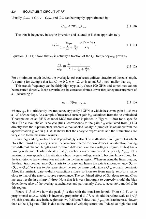
234 EQUIVALENT CIRCUIT AT RF
Usually CGBo < CGSo + CGDo and CGo can be roughly approximated by
CGo∼= 2W LovCox. (11.10)
The transit frequency in strong inversion and saturation is then approximately
ωt∼=
ωspec
1 − 13n
+ 2Lov
L f
n(VP − VS)
UT
. (11.11)
Equation (11.11) shows that ωt is actually a fraction of the QS frequency ωqs given by
ωt
ωqs
∼=4
15
n
1 − 13n
+ 2Lov
L f
. (11.12)
For a minimum length device, the overlap length can be a significant fraction of the gate length.
Assuming for example that Lov/L f = 0.2, n = 1.2, ωt is about 3.5 times smaller than ωqs.
This transit frequency can be fairly high (typically above 100 GHz) and sometimes cannot
be measured directly. It can nevertheless be extracted from a lower frequency measurement of
h21 according to
ωt = ℑh21ωspot, (11.13)
where ωspot is a sufficiently low frequency (typically 1 GHz) at which the current gain h21 shows
a −20 dB/dec slope. An example of measured current gain h21 calculated from the de-embedded
Y-parameters of an RF N-channel MOS transistor is plotted in Figure 11.3(a) for a specific
bias. The curve labeled “analytic (full)” corresponds to the gain h21 calculated from (11.3)
directly with the Y-parameters, whereas curve labeled “analytic (simple)” is obtained from the
approximation given in (11.3). It shows that the analytic expressions and the simulations are
very close to the measured results.
Since Gm and CG are both bias dependent, ft is also. This is illustrated in Figure 11.4 which
plots the transit frequency versus the inversion factor for two devices in saturation having
two different channel lengths and for three different drain bias voltages. Figure 11.4(a) has a
lin–log scale and clearly indicates that ft reaches a maximum called the peak ft ft-peak. This
maximum corresponds to the situation where the gate voltage starts to become large enough for
the transistor to leave saturation and enter in the linear region. When entering the linear region,
the drain transconductance Gmd starts to increase and hence the gate transconductance Gm =(Gms − Gmd)/n starts to decrease since the source transconductance Gms remains constant.
Also, the intrinsic gate-to-drain capacitance starts to increase from nearly zero to a value
close to that of the gate-to-source capacitance. The combined effect of Gm decrease and CGDi
increase results in a sharp ft drop. Note that it is very important to correctly model the bias
dependence also of the overlap capacitances and particularly CGDo to accurately model ft in
this region.
Figure 11.5 shows how the peak ft scales with the transistor length. From (11.4), ωt is
proportional to ωspec which is inversely proportional to L2f . ωt should therefore scale as 1/L2
f
which is about the case in the regions above 0.25 μm. Below that, ft-peak tends to increase slower
than at the 1/L2f rate. This is due to the effect of velocity saturation. Indeed, at high bias and
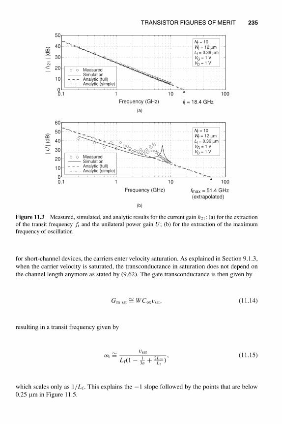
TRANSISTOR FIGURES OF MERIT 235
0.1 1 10 1000
10
20
30
40
50
Frequency (GHz)
MeasuredSimulationAnalytic (full)Analytic (simple)
Nf = 10Wf = 12 µmLf = 0.36 µmVG = 1 VVD = 1 V
| h
21 | (
dB
)
ft = 18.4 GHz
0.1 1 10 100
Frequency (GHz)
MeasuredSimulationAnalytic (full)Analytic (simple)
0
10
20
30
40
50
60
Nf = 10Wf = 12 µmLf = 0.36 µmVG = 1 VVD = 1 V|
U | (
dB
)
fmax = 51.4 GHz(extrapolated)
(a)
(b)
Figure 11.3 Measured, simulated, and analytic results for the current gain h21: (a) for the extraction
of the transit frequency ft and the unilateral power gain U ; (b) for the extraction of the maximum
frequency of oscillation
for short-channel devices, the carriers enter velocity saturation. As explained in Section 9.1.3,
when the carrier velocity is saturated, the transconductance in saturation does not depend on
the channel length anymore as stated by (9.62). The gate transconductance is then given by
Gm sat∼= WCoxvsat, (11.14)
resulting in a transit frequency given by
ωt∼=
vsat
L f(1 − 13n
+ 2Lov
L f), (11.15)
which scales only as 1/L f. This explains the −1 slope followed by the points that are below
0.25 μm in Figure 11.5.
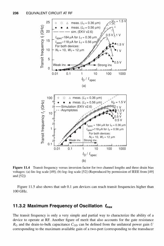
236 EQUIVALENT CIRCUIT AT RF
25
20
15
10
5
0Tra
nsit fre
quency f
t (G
Hz)
0.01 0.1 1 10 100 1000
ID / I spec
Weak inv. Strong inv.
0.5 V 1 V
VD = 1.5 V
1.5 V
1 V
0.5 V
meas. (L f = 0.36 µm)
meas. (L f = 0.56 µm)
sim. (EKV v2.6)
Ispec≈184 µA for L f = 0.36 µm
Ispec≈118 µA for L f = 0.56 µm
For both devices:
N f = 10, W f = 12 µm
0.12
4
1
2
4
10
2
4
100
Tra
nsit fre
quency f
t (G
Hz)
0.01 0.1 1 10 100 1000
ID / Ispec
Weak inv. Strong inv.
0.5 V
1 V
VD = 1.5 V
1.5 V1 V
0.5 V
meas. (L f = 0.36 µm)
meas. (L f = 0.56 µm)
Simulation (EKV v2.6)Asymptotes
Ispec = 184 µA for Lf = 0.36 µm
Ispec=118 µA for Lf = 0.56 µm
For both devices:
N f = 10, W f = 12 µm
(a)
(b)
Figure 11.4 Transit frequency versus inversion factor for two channel lengths and three drain bias
voltages: (a) lin–log scale [49]; (b) log–log scale [52] (Reproduced by permission of IEEE from [49]
and [52])
Figure 11.5 also shows that sub 0.1 μm devices can reach transit frequencies higher than
100 GHz.
11.3.2 Maximum Frequency of Oscillation fmax
The transit frequency is only a very simple and partial way to characterize the ability of a
device to operate at RF. Another figure of merit that also accounts for the gate resistance
RG and the drain-to-bulk capacitance CGD can be defined from the unilateral power gain U
corresponding to the maximum available gain of a two-port (corresponding to the transducer
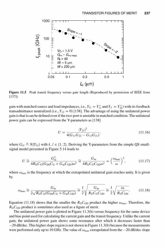
TRANSISTOR FIGURES OF MERIT 237
Figure 11.5 Peak transit frequency versus gate length (Reproduced by permission of IEEE from
[137])
gain with matched source and load impedances, i.e., YG = Y ∗11 and YL = Y ∗
22) with its feedback
transadmittance neutralized (i.e., Y12 = 0) [138]. The advantage of using the unilateral power
gain is that it can be defined even if the two-port is unstable in matched condition. The unilateral
power gain can be expressed from the Y-parameters as [138]
U =|Y21|2
4(G11G22 − G12G21), (11.16)
where Gkl ℜYkl with k, l ∈ 1, 2. Deriving the Y-parameters from the simple QS small-
signal model presented in Figure 5.14 leads to
U ∼=G2
m
4RGCG(GDSCG + GmCGD)ω2∼=
Gm
4RGCGCGDω2=
(ωmax
ω
)2
, (11.17)
where ωmax is the frequency at which the extrapolated unilateral gain reaches unity. It is given
by
ωmax∼=
Gm
2√
RGCG(GDSCG + GmCGD)∼=
1
2
√Gm
RGCGCGD
∼=1
2
√ωt
RGCGD
. (11.18)
Equation (11.18) shows that the smaller the RGCGD product the higher ωmax. Therefore, the
RGCGD product is sometimes also used as a figure of merit.
The unilateral power gain is plotted in Figure 11.3(b) versus frequency for the same device
and bias point used for calculating the current gain and the transit frequency. Unlike the current
gain, the unilateral power gain shows some resonance after which it decreases faster than
−20 dB/dec. This higher slope region is not shown in Figure 11.3(b) because the measurements
were performed only up to 10 GHz. The value of ωmax extrapolated from the −20 dB/dec slope
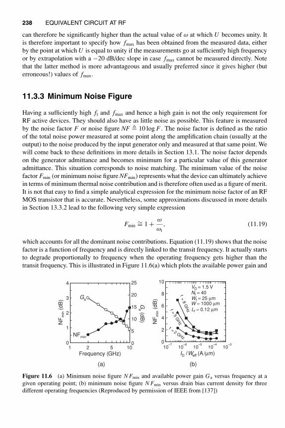
238 EQUIVALENT CIRCUIT AT RF
can therefore be significantly higher than the actual value of ω at which U becomes unity. It
is therefore important to specify how fmax has been obtained from the measured data, either
by the point at which U is equal to unity if the measurements go at sufficiently high frequency
or by extrapolation with a −20 dB/dec slope in case fmax cannot be measured directly. Note
that the latter method is more advantageous and usually preferred since it gives higher (but
erroneous!) values of fmax.
11.3.3 Minimum Noise Figure
Having a sufficiently high ft and fmax and hence a high gain is not the only requirement for
RF active devices. They should also have as little noise as possible. This feature is measured
by the noise factor F or noise figure NF 10 log F . The noise factor is defined as the ratio
of the total noise power measured at some point along the amplification chain (usually at the
output) to the noise produced by the input generator only and measured at that same point. We
will come back to these definitions in more details in Section 13.1. The noise factor depends
on the generator admittance and becomes minimum for a particular value of this generator
admittance. This situation corresponds to noise matching. The minimum value of the noise
factor Fmin (or minimum noise figure NFmin) represents what the device can ultimately achieve
in terms of minimum thermal noise contribution and is therefore often used as a figure of merit.
It is not that easy to find a simple analytical expression for the minimum noise factor of an RF
MOS transistor that is accurate. Nevertheless, some approximations discussed in more details
in Section 13.3.2 lead to the following very simple expression
Fmin∼= 1 +
ω
ωt
, (11.19)
which accounts for all the dominant noise contributions. Equation (11.19) shows that the noise
factor is a function of frequency and is directly linked to the transit frequency. It actually starts
to degrade proportionally to frequency when the operating frequency gets higher than the
transit frequency. This is illustrated in Figure 11.6(a) which plots the available power gain and
4
3
2
1
0
NF
min (
dB
)
1 2 5 10
Frequency (GHz)
25
20
15
10
5
0
Ga (d
B)
Ga
NFmin
f = 8
GH
zf = 5 G
Hz
f = 2 GHz
10–7
10–6
10–5
10–4
10–3
10
0
2
4
6
8
NF
min (
dB
)
(A/µm)I W
VD = 1.5 VNf = 40
Lf = 0.12 µm
Wf = 25 µmW = 1000 µm
(a) (b)
Figure 11.6 (a) Minimum noise figure N Fmin and available power gain Ga versus frequency at a
given operating point; (b) minimum noise figure N Fmin versus drain bias current density for three
different operating frequencies (Reproduced by permission of IEEE from [137])
TRANSISTOR FIGURES OF MERIT 239
the minimum noise figure verus frequency for a given operating point. This plot also illustrates
the fact that the minimum noise figure is obviously minimum when the gain is maximum.
Since the minimum noise figure depends on the transit frequency, it also depends on the
bias. Figure 11.6(b) shows the minimum noise figure versus the drain bias current density
(current per transistor width) for three different operating frequencies. It clearly shows that
there is an optimum bias point where NFmin is minimum. Note that this optimum bias occurs
about at the same current density for the three different frequencies.
11.3.4 Moderate and Weak Inversion for RF Circuits
The high transit frequency of ultradeep submicron (UDSM) CMOS processes can be traded
with power consumption to implement RF circuits operating in the gigahertz frequency range.
This can be done by moving the operating point from strong inversion to moderate or even
weak inversion, in order to spend just the required power to achieve the desired performance.
There are several advantages to bias the transistor in moderate or weak inversion. The first
advantage is the increase of the current efficiency (measured by the Gm/ID ratio) which results
in a further reduction of the power consumption. Secondly, the decrease of the bias voltages
results in lower electrical fields within the device. This avoids velocity saturation and hot
electron effects. Having no velocity saturation results in ft scaling as 1/L2f compared to only
1/L f when velocity saturation is present. This means that scaling is more effective for devices
biased in the weak and moderate inversion region than in strong inversion. Thirdly, having no
hot electron effects avoids the increase of the noise excess factor.
Finally, the reduction of the bias voltages better accommodates the use of low supply
voltages that are imposed by the scaling of UDSM technologies.
On the other hand, moving toward weak inversion changes the ID − VG characteristic from
a quasi-quadratic to an exponential function, which clearly degrades the device linearity. Mod-
erate inversion therefore represents a good trade-off between power consumption, noise, and
linearity.
Part of the power is just used to fight against the extrinsic components such as the overlap
and junction capacitances. There might be a concern that the time constants in moderate and
weak inversion might be completely dominated by these extrinsic components and therefore
counterbalance the advantage of the current efficiency increase. A way to investigate this issue
is by looking at the total transit time τt defined as τt 1/(2π ft), which can be decomposed
into τt τi + τe, where τi = CGi/Gm corresponds to the transit time of the intrinsic part with
CGi being the total gate intrinsic capacitance CGi = CGSi + CGDi + CGBi. The time constant
τi ultimately represents the lowest time constant the device can achieve for a given operating
point. The time constant τe corresponds to the additional delay introduced by the extrinsic part
of the device due to the overlap capacitances and the series resistances:
τe =CGo
Gm
+ RD CGD + n RS
(CGB + CGD +
n − 1
nCGS
), (11.20)
where CGo = CGSo + CGDo + CGBo is the total gate overlap capacitance. Usually the con-
tributions of the source and drain series resistances can be neglected and hence τe∼= CGo/
Gm.
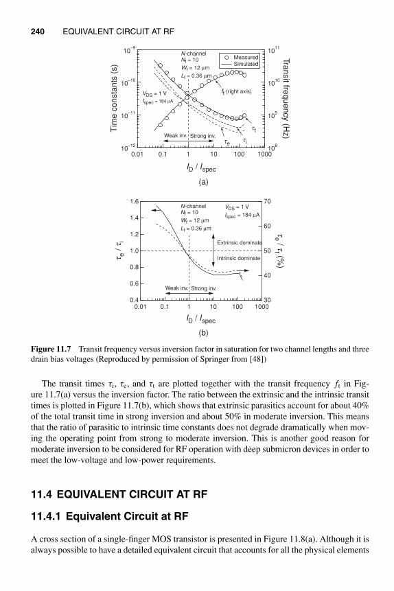
240 EQUIVALENT CIRCUIT AT RF
10–12
10–11
10–10
10–9
Tim
e c
onsta
nts
(s)
0.01 0.1 1 10 100 1000
ID / Ispec
108
109
1010
1011
Tra
nsit fre
quency (H
z)Strong inv.Weak inv.
Measured Simulated
tite
tt
ft (right axis)
N-channelNf = 10
Wf = 12 µm
Lf = 0.36 µm
VDS = 1 V
Ispec = 184 µA
1.6
1.4
1.2
1.0
0.8
0.6
0.4
t e / t
i
0.01 0.1 1 10 100 1000
70
60
50
40
30
te / t
t (%)
Strong inv.Weak inv.
Extrinsic dominate
Intrinsic dominate
VDS = 1 V
Ispec = 184 µA
N-channelNf = 10
Wf = 12 µm
Lf = 0.36 µm
ID / Ispec
(a)
(b)
Figure 11.7 Transit frequency versus inversion factor in saturation for two channel lengths and three
drain bias voltages (Reproduced by permission of Springer from [48])
The transit times τi, τe, and τt are plotted together with the transit frequency ft in Fig-
ure 11.7(a) versus the inversion factor. The ratio between the extrinsic and the intrinsic transit
times is plotted in Figure 11.7(b), which shows that extrinsic parasitics account for about 40%
of the total transit time in strong inversion and about 50% in moderate inversion. This means
that the ratio of parasitic to intrinsic time constants does not degrade dramatically when mov-
ing the operating point from strong to moderate inversion. This is another good reason for
moderate inversion to be considered for RF operation with deep submicron devices in order to
meet the low-voltage and low-power requirements.
11.4 EQUIVALENT CIRCUIT AT RF
11.4.1 Equivalent Circuit at RF
A cross section of a single-finger MOS transistor is presented in Figure 11.8(a). Although it is
always possible to have a detailed equivalent circuit that accounts for all the physical elements
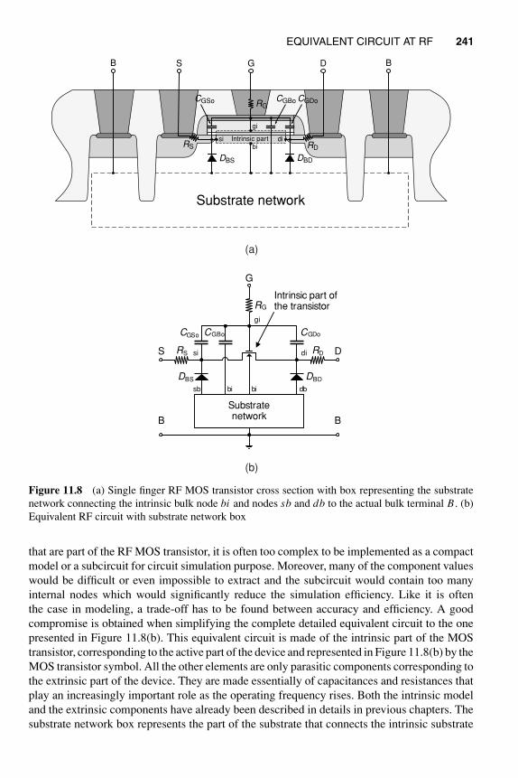
EQUIVALENT CIRCUIT AT RF 241
bi
GB BS D
RGCGDoCGBo
DBDDBS
CGSo
RDRSsi Intrinsic part di
gi
Substrate network
RDRS
CGBoCGSo CGDo
RG
G
S D
gi
disi
Intrinsic part of the transistor
DBS DBD
Substratenetwork B
bi
B
sb dbbi
(a)
(b)
Figure 11.8 (a) Single finger RF MOS transistor cross section with box representing the substrate
network connecting the intrinsic bulk node bi and nodes sb and db to the actual bulk terminal B. (b)
Equivalent RF circuit with substrate network box
that are part of the RF MOS transistor, it is often too complex to be implemented as a compact
model or a subcircuit for circuit simulation purpose. Moreover, many of the component values
would be difficult or even impossible to extract and the subcircuit would contain too many
internal nodes which would significantly reduce the simulation efficiency. Like it is often
the case in modeling, a trade-off has to be found between accuracy and efficiency. A good
compromise is obtained when simplifying the complete detailed equivalent circuit to the one
presented in Figure 11.8(b). This equivalent circuit is made of the intrinsic part of the MOS
transistor, corresponding to the active part of the device and represented in Figure 11.8(b) by the
MOS transistor symbol. All the other elements are only parasitic components corresponding to
the extrinsic part of the device. They are made essentially of capacitances and resistances that
play an increasingly important role as the operating frequency rises. Both the intrinsic model
and the extrinsic components have already been described in details in previous chapters. The
substrate network box represents the part of the substrate that connects the intrinsic substrate
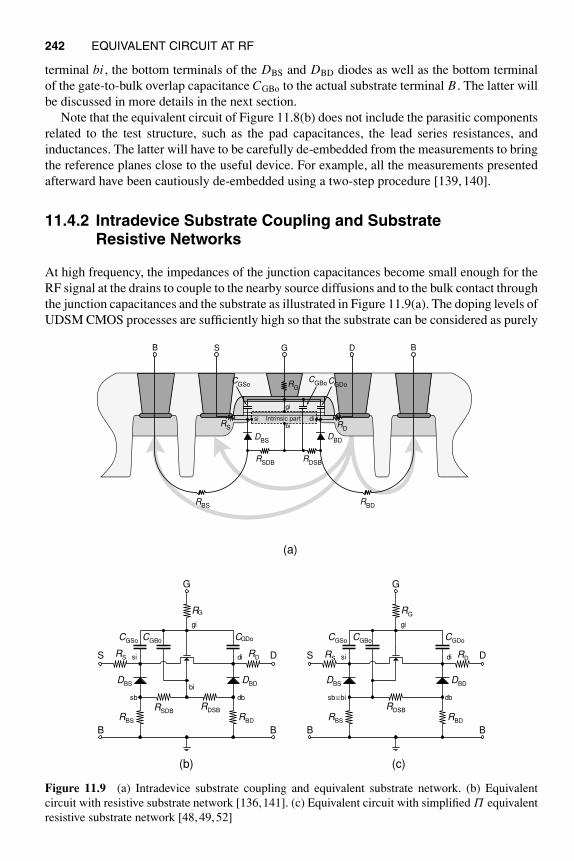
242 EQUIVALENT CIRCUIT AT RF
terminal bi , the bottom terminals of the DBS and DBD diodes as well as the bottom terminal
of the gate-to-bulk overlap capacitance CGBo to the actual substrate terminal B. The latter will
be discussed in more details in the next section.
Note that the equivalent circuit of Figure 11.8(b) does not include the parasitic components
related to the test structure, such as the pad capacitances, the lead series resistances, and
inductances. The latter will have to be carefully de-embedded from the measurements to bring
the reference planes close to the useful device. For example, all the measurements presented
afterward have been cautiously de-embedded using a two-step procedure [139, 140].
11.4.2 Intradevice Substrate Coupling and SubstrateResistive Networks
At high frequency, the impedances of the junction capacitances become small enough for the
RF signal at the drains to couple to the nearby source diffusions and to the bulk contact through
the junction capacitances and the substrate as illustrated in Figure 11.9(a). The doping levels of
UDSM CMOS processes are sufficiently high so that the substrate can be considered as purely
bi
GB BS D
RG
CGDo
CGBo
DBDD
BS
CGSo
RD
RS
RSDB
RDSB
RBS
RBD
si Intrinsic part di
gi
RDRS
CGBoCGSo CGDo
RG
G
S D
gi
disi
DBS DBD
B
bi
B
RSDBRDSB
RBS RBD
sb db
RDRS
CGBoCGSo CGDo
RG
G
S D
gi
disi
DBS DBD
BB
RDSB
RBS RBD
sb≡bi db
(a)
(b) (c)
Figure 11.9 (a) Intradevice substrate coupling and equivalent substrate network. (b) Equivalent
circuit with resistive substrate network [136,141]. (c) Equivalent circuit with simplified Π equivalent
resistive substrate network [48, 49, 52]
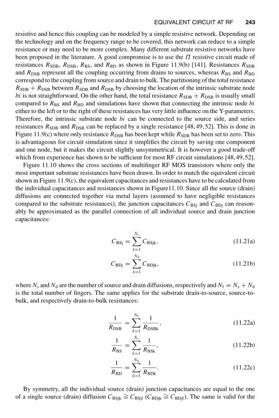
EQUIVALENT CIRCUIT AT RF 243
resistive and hence this coupling can be modeled by a simple resistive network. Depending on
the technology and on the frequency range to be covered, this network can reduce to a simple
resistance or may need to be more complex. Many different substrate resistive networks have
been proposed in the literature. A good compromise is to use the Π resistive circuit made of
resistances RSDB, RDSB, RBS, and RBD as shown in Figure 11.9(b) [141]. Resistances RSDB
and RDSB represent all the coupling occurring from drains to sources, whereas RBS and RBD
correspond to the coupling from source and drain to bulk. The partitioning of the total resistance
RSDB + RDSB between RSDB and RDSB by choosing the location of the intrinsic substrate node
bi is not straightforward. On the other hand, the total resistance RSDB + RDSB is usually small
compared to RBS and RBD and simulations have shown that connecting the intrinsic node bi
either to the left or to the right of these resistances has very little influence on the Y-parameters.
Therefore, the intrinsic substrate node bi can be connected to the source side, and series
resistances RSDB and RDSB can be replaced by a single resistance [48, 49, 52]. This is done in
Figure 11.9(c) where only resistance RDSB has been kept while RSDB has been set to zero. This
is advantageous for circuit simulation since it simplifies the circuit by saving one component
and one node, but it makes the circuit slightly unsymmetrical. It is however a good trade-off
which from experience has shown to be sufficient for most RF circuit simulations [48,49,52].
Figure 11.10 shows the cross sections of multifinger RF MOS transistors where only the
most important substrate resistances have been drawn. In order to match the equivalent circuit
shown in Figure 11.9(c), the equivalent capacitances and resistances have to be calculated from
the individual capacitances and resistances shown in Figure11.10. Since all the source (drain)
diffusions are connected together via metal layers (assumed to have negligible resistances
compared to the substrate resistances), the junction capacitances CBSj and CBDj can reason-
ably be approximated as the parallel connection of all individual source and drain junction
capacitances:
CBSj =Ns∑
k=1
CBSjk, (11.21a)
CBDj =Nd∑
k=1
CBDjk, (11.21b)
where Ns and Nd are the number of source and drain diffusions, respectively and Nf = Ns + Nd
is the total number of fingers. The same applies for the substrate drain-to-source, source-to-
bulk, and respectively drain-to-bulk resistances:
1
RDSB
=Nf∑
k=1
1
RDSBk
, (11.22a)
1
RBS
=Ns∑
k=1
1
RBSk
, (11.22b)
1
RBD
=Nd∑
k=1
1
RBDk
. (11.22c)
By symmetry, all the individual source (drain) junction capacitances are equal to the one
of a single source (drain) diffusion CBSjk∼= CBSjf (CBDjk
∼= CBDjf). The same is valid for the
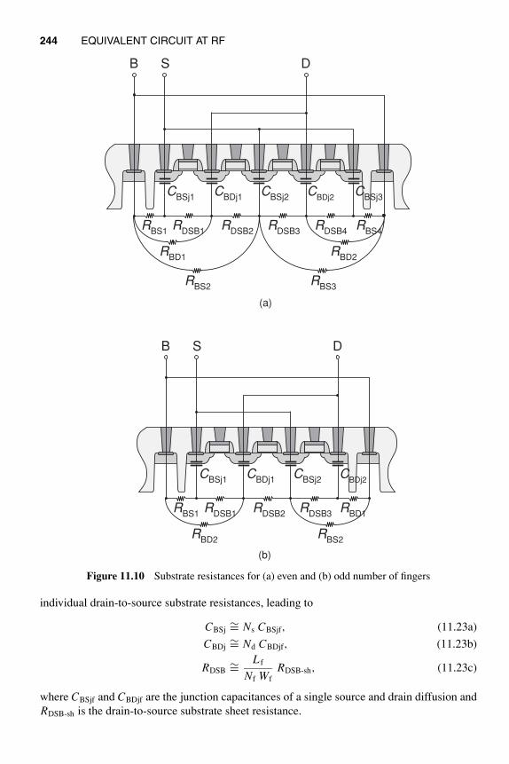
244 EQUIVALENT CIRCUIT AT RF
B S D
CBSj1
RDSB1
RBS1
RBD1
RBS2
RBS3
RBD2
RDSB2
RDSB3
RDSB4
RBS4
CBDj1
CBSj2
CBDj2
CBSj3
B S D
CBSj1
RDSB1
RBS1
RBD2
RBS2
RDSB2
RDSB3
RBD1
CBDj1
CBSj2
CBDj2
(a)
(b)
Figure 11.10 Substrate resistances for (a) even and (b) odd number of fingers
individual drain-to-source substrate resistances, leading to
CBSj∼= Ns CBSjf, (11.23a)
CBDj∼= Nd CBDjf, (11.23b)
RDSB∼=
L f
Nf Wf
RDSB-sh, (11.23c)
where CBSjf and CBDjf are the junction capacitances of a single source and drain diffusion and
RDSB-sh is the drain-to-source substrate sheet resistance.
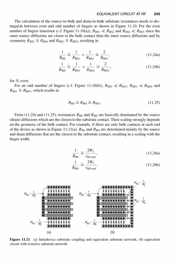
EQUIVALENT CIRCUIT AT RF 245
The calculation of the source-to-bulk and drain-to-bulk substrate resistances needs to dis-
tinguish between even and odd number of fingers as shown in Figure 11.10. For the even
number of fingers transistor (c.f. Figure 11.10(a)), RBS1 ≪ RBS2 and RBS4 ≪ RBS3 since the
outer source diffusions are closer to the bulk contact than the inner source diffusions and by
symmetry RBS1∼= RBS4 and RBD1
∼= RBD2, resulting in
1
RBS
∼=1
RBS1
+1
RBS4
∼=2
RBS1
, (11.24a)
1
RBD
∼=1
RBD1
+1
RBD2
∼=2
RBD1
, (11.24b)
for Nf even.
For an odd number of fingers (c.f. Figure 11.10(b)), RBS1 ≪ RBS2, RBD1 ≪ RBD2 and
RBS1∼= RBD1, which results in
RBS∼= RBD
∼= RBS1. (11.25)
From (11.24) and (11.25), resistances RBS and RBD are basically dominated by the source
(drain) diffusions which are the closest to the substrate contact. Their scaling strongly depends
on the geometry of the bulk contact. For example, if there are only bulk contacts at each end
of the device as shown in Figure 11.11(a), RBS and RBD are determined mainly by the source
and drain diffusions that are the closest to the substrate contact, resulting in a scaling with the
finger width
1
RBS
∼=2Wf
rBS-end
, (11.26a)
1
RBD
∼=2Wf
rBD-end
, (11.26b)
RBD ~1Wf
RBS ~1Wf
RBS ~1Ns
RBD ~1Nd
RBS ~1Wf
RBD ~1Wf
(a) (b)
Figure 11.11 (a) Intradevice substrate coupling and equivalent substrate network; (b) equivalent
circuit with resistive substrate network
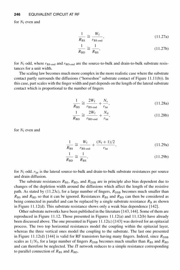
246 EQUIVALENT CIRCUIT AT RF
for Nf even and
1
RBS
∼=Wf
rBS-end
, (11.27a)
1
RBD
∼=1
RBS
, (11.27b)
for Nf odd, where rBS-end and rBD-end are the source-to-bulk and drain-to-bulk substrate resis-
tances for a unit width.
The scaling law becomes much more complex in the more realistic case where the substrate
contact partly surrounds the diffusions (“horseshoe” substrate contact of Figure 11.11(b)). In
this case, part scales with the finger width and part depends on the length of the lateral substrate
contact which is proportional to the number of fingers
1
RBS
∼=2Wf
rBS-end
+Ns
rlat
, (11.28a)
1
RBD
∼=2Wf
rBD-end
+Nd
rlat
, (11.28b)
for Nf even and
1
RBS
∼=Wf
rBS-end
+(Nf + 1)/2
rlat
, (11.29a)
1
RBD
∼=1
RBS
, (11.29b)
for Nf odd. rlat is the lateral source-to-bulk and drain-to-bulk substrate resistances per source
and drain diffusion.
The substrate resistances RBS, RBD, and RDSB are in principle also bias dependent due to
changes of the depletion width around the diffusions which affect the length of the resistive
path. As stated by (11.23c), for a large number of fingers, RDSB becomes much smaller than
RBS and RBD so that it can be ignored. Resistances RBS and RBD can then be considered as
being connected in parallel and can be replaced by a single substrate resistance RB as shown
in Figure 11.12(d). This substrate resistance shows only a weak bias dependence [142].
Other substrate networks have been published in the literature [143,144]. Some of them are
reproduced in Figure 11.12. Those presented in Figures 11.12(a) and 11.12(b) have already
been discussed above. The one presented in Figure 11.12(c) [143] was derived for an epitaxial
process. The two top horizontal resistances model the coupling within the epitaxial layer,
whereas the three vertical ones model the coupling to the substrate. The last one presented
in Figure 11.12(d) [144] is valid for RF transistors having many fingers. Indeed, since RDSB
scales as 1/Nf, for a large number of fingers RDSB becomes much smaller than RBS and RBD
and can therefore be neglected. The Π network reduces to a simple resistance corresponding
to parallel connection of RBS and RBD.
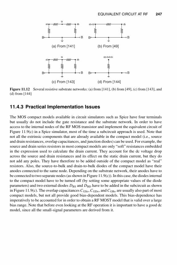
EQUIVALENT CIRCUIT AT RF 247
B
bi
B
sb db
BB
db
B
bi
B
sb db
B
sb≡bd≡bi
B
(a) From [141]
(c) From [143]
(b) From [49]
(d) From [144]
sb≡bi
Figure 11.12 Several resistive substrate networks: (a) from [141], (b) from [49], (c) from [143], and
(d) from [144]
11.4.3 Practical Implementation Issues
The MOS compact models available in circuit simulators such as Spice have four terminals
but usually do not include the gate resistance and the substrate network. In order to have
access to the internal nodes of the RF MOS transistor and implement the equivalent circuit of
Figure 11.9(c) in a Spice simulator, most of the time a subcircuit approach is used. Note that
not all the extrinsic components that are already available in the compact model (i.e., source
and drain resistances, overlap capacitances, and junction diodes) can be used. For example, the
source and drain series resistors in most compact models are only “soft” resistances embedded
in the expression used to calculate the drain current. They account for the dc voltage drop
across the source and drain resistances and its effect on the static drain current, but they do
not add any poles. They have therefore to be added outside of the compact model as “real”
resistors. Also, the source-to-bulk and drain-to-bulk diodes of the compact model have their
anodes connected to the same node. Depending on the substrate network, their anodes have to
be connected to two separate nodes (as shown in Figure 11.9(c)). In this case, the diodes internal
to the compact model have to be turned off (by setting some appropriate values of the diode
parameters) and two external diodes DBS and DBD have to be added in the subcircuit as shown
in Figure 11.9(c). The overlap capacitances CGSo, CGDo, and CGBo are usually also part of most
compact models, but not all provide good bias-dependent models. This bias-dependence has
imperatively to be accounted for in order to obtain a RF MOST model that is valid over a large
bias range. Note that before even looking at the RF operation it is important to have a good dc
model, since all the small-signal parameters are derived from it.

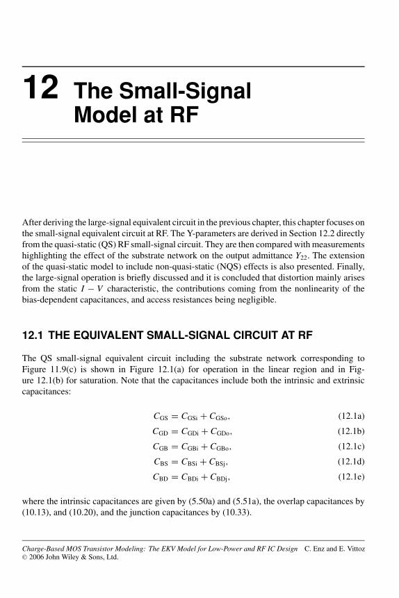
12 The Small-SignalModel at RF
After deriving the large-signal equivalent circuit in the previous chapter, this chapter focuses on
the small-signal equivalent circuit at RF. The Y-parameters are derived in Section 12.2 directly
from the quasi-static (QS) RF small-signal circuit. They are then compared with measurements
highlighting the effect of the substrate network on the output admittance Y22. The extension
of the quasi-static model to include non-quasi-static (NQS) effects is also presented. Finally,
the large-signal operation is briefly discussed and it is concluded that distortion mainly arises
from the static I − V characteristic, the contributions coming from the nonlinearity of the
bias-dependent capacitances, and access resistances being negligible.
12.1 THE EQUIVALENT SMALL-SIGNAL CIRCUIT AT RF
The QS small-signal equivalent circuit including the substrate network corresponding to
Figure 11.9(c) is shown in Figure 12.1(a) for operation in the linear region and in Fig-
ure 12.1(b) for saturation. Note that the capacitances include both the intrinsic and extrinsic
capacitances:
CGS = CGSi + CGSo, (12.1a)
CGD = CGDi + CGDo, (12.1b)
CGB = CGBi + CGBo, (12.1c)
CBS = CBSi + CBSj, (12.1d)
CBD = CBDi + CBDj, (12.1e)
where the intrinsic capacitances are given by (5.50a) and (5.51a), the overlap capacitances by
(10.13), and (10.20), and the junction capacitances by (10.33).
Charge-Based MOS Transistor Modeling: The EKV Model for Low-Power and RF IC Design C. Enz and E. VittozC© 2006 John Wiley & Sons, Ltd.
250 THE SMALL-SIGNAL MODEL AT RF
Im
Ims
Gds
disi
CGS CGD
CBS CBD
RS RD
CGB
RG
S
B
RDSB
RBS RBD
I1
bi
Ggi
D
B
I2V1
V2
(a) (b)
Im
Ims
Imd
Gds
disi
CGS CGD
CBS CBD
RS RD
CGB
RG
S
B
RDSB
RBS RBD
I1
bi
Ggi
D
B
I2
V1
V2
Figure 12.1 Equivalent RF small-signal circuit: (a) in the linear region; (b) in saturation
The voltage-controlled current sources (VCCS) are defined by
Im Ym [V (gi) − V (bi)], (12.2a)
Ims Yms [V (si) − V (bi)], (12.2b)
Imd Ymd [V (di) − V (bi)], (12.2c)
where V (k) with k ∈ gi, si, di, bi stands for the potential at node k. The transadmittances Ym,
Yms and Ymd are given by (5.58), (5.56), and (5.57), which are repeated here for convenience:
Ym = Gm (1 − j ωτqs) = Gm − j ω Cm, (12.3a)
Yms = Gms (1 − j ωτqs) = Gms − j ω Cms, (12.3b)
Ymd = Gmd (1 − j ωτqs) = Gmd − j ω Cmd. (12.3c)
Remember that the gate transadmittance, transconductance, and transcapacitance are related
to the source and drain transadmittances, transconductances, and transcapacitances according
to (5.37), (5.9), and (5.59):
Ym =Yms − Ymd
n, (12.4a)
Gm =Gms − Gmd
n, (12.4b)
Cm =Cms − Cmd
n. (12.4c)
Y-PARAMETERS ANALYSIS 251
12.2 Y-PARAMETERS ANALYSIS
The small-signal behavior of RF MOS transistors at high frequency is validated by measuring
the S-parameters versus frequency at several operating points of a single transistor connected
in common source as shown in Figure 12.1 by the dashed line. The S-parameters are usually
measured directly on wafer using probes connecting the pads. Most often the input and output
ports are connected by ground-signal-ground or GSG probes. The measured S-parameters
therefore also include the effect of the RF pads used to connect the device. The effects of
the pads have then to be de-embedded from the measured S-parameters using either a one-,
two- or even a three-step procedure [139, 140] in order to move the reference planes from the
end of the tips to the gate and drain nodes. The measurements shown below used a two-step
de-embedding procedure which is usually sufficient for measurements up to 10 GHz. The two-
step de-embedding procedure requires the measurement of the open and short structures. The
open structure is simply the same as the RF MOS transistor except that the RF MOS transistor
is taken out leaving the gate and drain open. The short structure is the same but now the RF
MOS transistor is replaced by a short circuit between the gate and the drain.
For convenience, the de-embedded S-parameters can then be transformed into Y-parameters
which are often easier to analyze [138, 145, 146]. The measured Y-parameters can then be
compared either to the analytical or eventually the simulated Y-parameters corresponding to
the equivalent circuit shown in Figure 11.9(c).
The equivalent small-signal circuit in saturation of Figure 12.1(b) will be validated by first
deriving the corresponding analytical Y-parameters and comparing them to the de-embedded
measurements. Since the capacitances are all approximately proportional to the total gate width
W = Nf Wf and since the source and drain terminal resistances are inversely proportional to W
(see (10.4)), the time constants due to the terminal resistances depend only on the gate length
L f, the overlap length Lov, or the diffusion width Hdif. The latter dimensions are usually taken
as minimum to achieve the highest cutoff frequency. Therefore the poles due to the terminal
resistances are at a much higher frequency than typically the transit frequency, so that they can
be basically neglected when calculating the Y-parameters and the related quantities. Neglecting
the substrate resistances also in the small-signal circuit of Figure 12.1(b) (i.e., assuming that
they are zero) allows to derive the following analytical expressions for the Y-parameters in
saturation:
Y11∼=
j ωCG
1 + j ωRGCG
, (12.5a)
Y12∼=
−j ωCGD
1 + j ωRGCG
, (12.5b)
Y21∼=
Gm − j ω(CGD + Cm)
1 + j ωRGCG
, (12.5c)
Y22∼=
Gds + ω2 RGCGDCm + j ω(CGD + CBD)
1 + j ωRGCG
, (12.5d)
where it has been assumed that Gm RG ≪ 1 and Gds ≪ Gm. Capacitance CG is the total ca-
pacitance at the gate
CG CGS + CGD + CGB, (12.6)
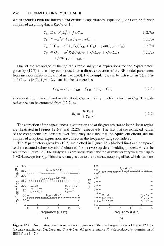
252 THE SMALL-SIGNAL MODEL AT RF
which includes both the intrinsic and extrinsic capacitances. Equation (12.5) can be further
simplified assuming that ωRGCG ≪ 1:
Y11∼= ω2 RGC2
G + j ωCG, (12.7a)
Y12∼= −ω2 RGCGDCG − j ωCGD, (12.7b)
Y21∼= Gm − ω2 RGCG(CGD + Cm) − j ω(CGD + Cm), (12.7c)
Y22∼= Gds + ω2 RG(CGCBD + CGCGD + CGDCm) (12.7d)
+ j ω(CBD + CGD).
One of the advantage of having the simple analytical expressions for the Y-parameters
given by (12.7) is that they can be used for a direct extraction of the RF model parameters
from measurements as presented in [147,148]. For example, CG can be extracted as ℑY11/ω
and CGD as |ℑY12|/ω. CGS can then be extracted as
CGS = CG − CGD − CGB∼= CG − CGD, (12.8)
since in strong inversion and in saturation, CGB is usually much smaller than CGS. The gate
resistance can be extracted from (12.7) as
RG =ℜY11
ℑY112. (12.9)
The extraction of the capacitances in saturation and of the gate resistance in the linear region
are illustrated in Figures 12.2(a) and 12.2(b) respectively. The fact that the extracted values
of the components are constant over frequency indicates that the equivalent circuit and the
simplified analytical expressions are correct in the frequency range considered.
The Y-parameters given by (12.7) are plotted in Figure 12.3 (dashed line) and compared
to the measured values (symbols) obtained from a two-step de-embedding process. As can be
seen from Figure 12.3, the analytical expressions match the measurements very well even up to
10 GHz except for Y22. This discrepancy is due to the substrate coupling effect which has been
400
350
300
250
200
150
100
50
01098765
Frequency (GHz)
CG = 325.5 fF
CGD = 79.8 fF
CGB + CGS = 245.7 fF
CG
, C
GB +
CG
S,
CG
D (
fF)
VG = 1.18 VVD = 1 VVS = 0 V
5.0
4.5
4.0
3.5
3.0
2.5
2.0
1.5
1.0
0.5
0.01098765
Frequency (GHz)
VG = 3 VVD = 0 VVS = 0 V
Nf = 20Wf = 10 µm
Lf = 0.5 µm
Nf = 20Wf = 10 µm
Lf = 0.5 µm
RG
(Ω
)
RG = 4.27 Ω
(a) (b)
Figure 12.2 Direct extraction of some of the components of the small-signal circuit of Figure 12.1(b):
(a) gate capacitances CG, CGD, and CGB + CGS; (b) gate resistance RG (Reproduced by permission of
IEEE from [147])
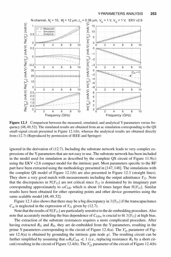
Y-PARAMETERS ANALYSIS 253
–0.2
0
0.2
–3
–2
–1
0
0
10
20
30
–8
–6
–4
–2
0
0 2 4 6 8 10
0 2 4 6 8 10
0 2 4 6 8 10
0 2 4 6 8 10
0 2 4 6 8 10
0 2 4 6 8 10
0 2 4 6 8 10
0 2 4 6 8 10
0
1.0
2.02.5
1.5
0.5
Frequency (GHz) Frequency (GHz)
ReY
22
(mA
/V)
Im Y
22
(mA
/V)
ImY
21
(mA
/V)I
mY
12
(mA
/V)Im
Y11
(m
A/V
)
ReY
21
(mA
/V)
ReY
12
(mA
/V)
ReY
11
(mA
/V)
0
2
4
6
8
0
0.5
1
0
5
10
15
m
Measured SimulationAnalytical
C =
N W L V V V V
Figure 12.3 Comparison between the measured, simulated, and analytical Y-parameters versus fre-
quency [48,49,52]. The simulated results are obtained from an ac simulation corresponding to the QS
small-signal circuit presented in Figure 12.1(b), whereas the analytical results are obtained directly
from (12.7) (Reproduced by permission of IEEE and Springer)
ignored in the derivation of (12.7). Including the substrate network leads to very complex ex-
pressions of the Y-parameters that are not easy to use. The substrate network has been included
in the model used for simulation as described by the complete QS circuit of Figure 11.9(c)
using the EKV v2.6 compact model for the intrinsic part. Most parameters specific to the RF
part have been extracted using the methodology presented in [147,148]. The simulations with
the complete QS model of Figure 12.1(b) are also presented in Figure 12.3 (straight lines).
They show a very good match with measurements including the output admittance Y22. Note
that the discrepancies in ℜY12 are not critical since Y12 is dominated by its imaginary part
corresponding approximately to ωCGD which is about 10 times larger than ℜY12. Similar
results have been obtained for other operating points and other device geometries using the
same scalable model [48, 49, 52].
Figure 12.3 also shows that there may be a big discrepancy in ℑY21 if the transcapacitance
Cm is neglected in the expression of Y21 given by (12.7).
Note that the results of ℜY11 are particularly sensitive to the de-embedding procedure. Also
note that accurately modeling the bias dependence of CGDo is crucial to fit ℑY12 at high bias.
The extraction of the substrate resistances requires a more complicated procedure. After
having extracted RG and RD, they are de-embedded from the Y-parameters, resulting in the
prime Y-parameters corresponding to the circuit of Figure 12.4(a). The Y ′22 parameter of Fig-
ure 12.4(a) is obtained by grounding the intrinsic gate node gi . The resulting circuit can be
further simplified by assuming that ωRSCGS ≪ 1 (i.e., replacing resistance RS by a short cir-
cuit) resulting in the circuit of Figure 12.4(b). The Y ′22 parameter of the circuit of Figure 12.4(b)
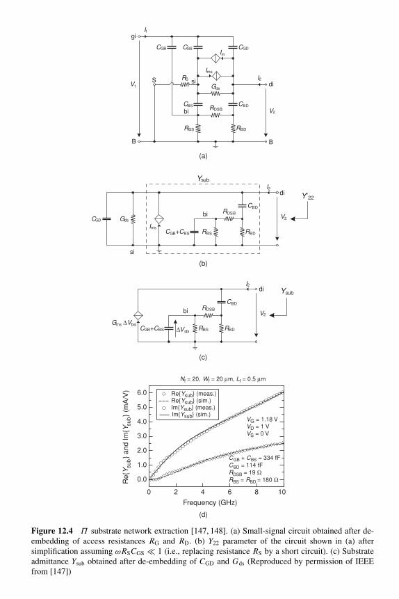
Im
Ims
Gds
si
CGS CGD
CBS CBD
RS
CGB
S
B
RDSB
RBS RBD
I1
bi
gi
di
B
I2V1
V2
Gds
CGB+CBS
CBDRDSB
RBS RBD
diI2
V2
Ims
CGD
si
bi
Ysub
Y’22
CGB+CBS
CBD
RDSB
RBS RBD
diI2
V2
Gms ∆Vbsi
bi
Ysub
∆Vsbi
6.0
5.0
4.0
3.0
2.0
1.0
0.0
1086420
Frequency (GHz)
ReYsub (meas.) ReYsub (sim.) ImYsub (meas.) ImYsub (sim.)
ReY
su
b
and Im
Ysu
b
(mA
/V)
VG = 1.18 VVD = 1 VVS = 0 V
(a)
(b)
(c)
(d)
CGB + CBS = 334 fF
CBD = 114 fF
RDSB = 19 Ω
RBS = RBD = 180 Ω
Nf = 20 Wf = 20 µm, Lf = 0.5 µm
Figure 12.4 Π substrate network extraction [147, 148]. (a) Small-signal circuit obtained after de-
embedding of access resistances RG and RD. (b) Y22 parameter of the circuit shown in (a) after
simplification assuming ωRSCGS ≪ 1 (i.e., replacing resistance RS by a short circuit). (c) Substrate
admittance Ysub obtained after de-embedding of CGD and Gds (Reproduced by permission of IEEE
from [147])
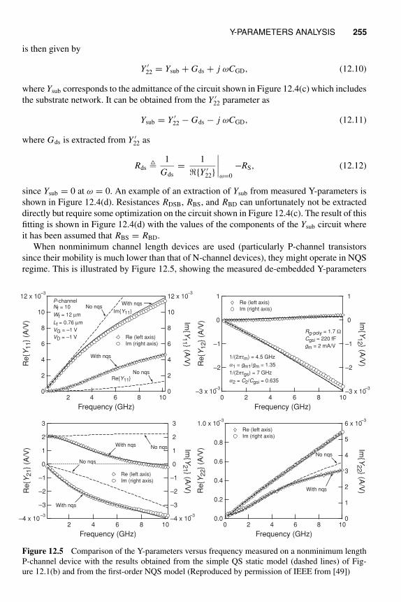
Y-PARAMETERS ANALYSIS 255
is then given by
Y ′22 = Ysub + Gds + j ωCGD, (12.10)
where Ysub corresponds to the admittance of the circuit shown in Figure 12.4(c) which includes
the substrate network. It can be obtained from the Y ′22 parameter as
Ysub = Y ′22 − Gds − j ωCGD, (12.11)
where Gds is extracted from Y ′22 as
Rds 1
Gds
=1
ℜY ′22
∣∣∣∣ω=0
−RS, (12.12)
since Ysub = 0 at ω = 0. An example of an extraction of Ysub from measured Y-parameters is
shown in Figure 12.4(d). Resistances RDSB, RBS, and RBD can unfortunately not be extracted
directly but require some optimization on the circuit shown in Figure 12.4(c). The result of this
fitting is shown in Figure 12.4(d) with the values of the components of the Ysub circuit where
it has been assumed that RBS = RBD.
When nonminimum channel length devices are used (particularly P-channel transistors
since their mobility is much lower than that of N-channel devices), they might operate in NQS
regime. This is illustrated by Figure 12.5, showing the measured de-embedded Y-parameters
–3 x 10⁻³
–2
–1
0
1
Re
Y1
2
(A/V
)
1086420
Frequency (GHz)
–3 x 10⁻³
–2
–1
0
1
ImY
12 (A
/V)
Re (left axis) Im (right axis)
1/(2ptm) = 4.5 GHz
a1 = gm1/gm = 1.35
1/(2ptgs) = 7 GHz
a2 = C2/Cgsi = 0.635
Rg-poly = 1.7 Ω
Cgsi = 220 fF
gm = 2 mA/V
1.0 x 10⁻³
0.8
0.6
0.4
0.2
0.0
Re
Y2
2
(A/V
)
1086420
Frequency (GHz)
6 x 10⁻³
5
4
3
2
1
0
ImY
22 (A
/V)
Re (left axis) Im (right axis)
No nqs
With nqs
–4 x 10⁻³
–3
–2
–1
0
1
2
3
Re
Y2
1
(A/V
)
108642
Frequency (GHz)
–4 x 10⁻³
–3
–2
–1
0
1
2
3
ImY
21 (A
/V)
Re (left axis) Im (right axis)
No nqsWith nqs
No nqs
With nqs
12 x 10–3
10
8
6
4
2
0
Re
Y1
1
(A/V
)
108642
Frequency (GHz)
12 x 10–3
10
8
6
4
2
0
ImY
11 (A
/V)
P-channelNf = 10
Wf = 12 µm
Lf = 0.76 µm
VG = –1 V
VD = –1 V Re (left axis) Im (right axis)
No nqsReY11
ImY11
With nqs
No nqsWith nqs
Figure 12.5 Comparison of the Y-parameters versus frequency measured on a nonminimum length
P-channel device with the results obtained from the simple QS static model (dashed lines) of Fig-
ure 12.1(b) and from the first-order NQS model (Reproduced by permission of IEEE from [49])
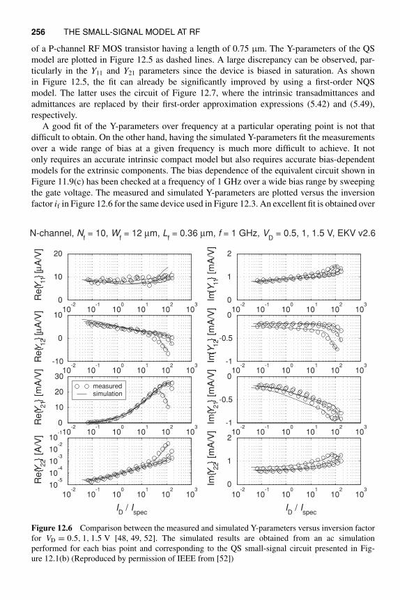
256 THE SMALL-SIGNAL MODEL AT RF
of a P-channel RF MOS transistor having a length of 0.75 μm. The Y-parameters of the QS
model are plotted in Figure 12.5 as dashed lines. A large discrepancy can be observed, par-
ticularly in the Y11 and Y21 parameters since the device is biased in saturation. As shown
in Figure 12.5, the fit can already be significantly improved by using a first-order NQS
model. The latter uses the circuit of Figure 12.7, where the intrinsic transadmittances and
admittances are replaced by their first-order approximation expressions (5.42) and (5.49),
respectively.
A good fit of the Y-parameters over frequency at a particular operating point is not that
difficult to obtain. On the other hand, having the simulated Y-parameters fit the measurements
over a wide range of bias at a given frequency is much more difficult to achieve. It not
only requires an accurate intrinsic compact model but also requires accurate bias-dependent
models for the extrinsic components. The bias dependence of the equivalent circuit shown in
Figure 11.9(c) has been checked at a frequency of 1 GHz over a wide bias range by sweeping
the gate voltage. The measured and simulated Y-parameters are plotted versus the inversion
factor if in Figure 12.6 for the same device used in Figure 12.3. An excellent fit is obtained over
0
10
20
0
1
2
-10
0
10
-1
-0.5
0
0
10
20
30
-1
-0.5
0
0
1
2
ID / I
spec
10-5
10-4
10-3
10-2
10-1
10-2
10-1
100
101
102
103
10-2
10-1
100
101
102
103
10-2
10-1
100
101
102
103
10-2
10-1
100
101
102
103
ID / I
spec
10-2
10-1
100
101
102
103
10-2
10-1
100
101
102
103
10-2
10-1
100
101
102
103
10-2
10-1
100
101
102
103
Re
Y22
[A/V
]R
e Y
21
[mA
/V]
Re
Y12
[µA
/V]
Re
Y11
[µA
/V]
Im Y
22
[mA
/V]
Im Y
21
[mA
/V]
Im Y
12
[mA
/V]
Im Y
11
[mA
/V]
N-channel, Nf = 10, W
f = 12 µm, L
f = 0.36 µm, f = 1 GHz, V
D = 0.5, 1, 1.5 V, EKV v2.6
measured simulation
Figure 12.6 Comparison between the measured and simulated Y-parameters versus inversion factor
for VD = 0.5, 1, 1.5 V [48, 49, 52]. The simulated results are obtained from an ac simulation
performed for each bias point and corresponding to the QS small-signal circuit presented in Fig-
ure 12.1(b) (Reproduced by permission of IEEE from [52])
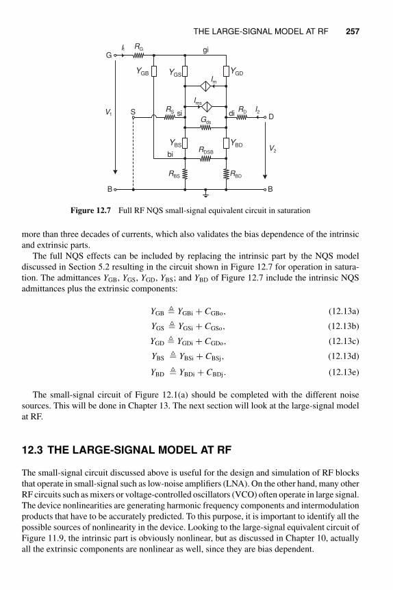
THE LARGE-SIGNAL MODEL AT RF 257
Im
Ims
Gds
disiRS RD
RG
S
B
RDSB
RBS RBD
I1
bi
Ggi
D
B
I2V1
V2
YGB YGSYGD
YBS YBD
Figure 12.7 Full RF NQS small-signal equivalent circuit in saturation
more than three decades of currents, which also validates the bias dependence of the intrinsic
and extrinsic parts.
The full NQS effects can be included by replacing the intrinsic part by the NQS model
discussed in Section 5.2 resulting in the circuit shown in Figure 12.7 for operation in satura-
tion. The admittances YGB, YGS, YGD, YBS; and YBD of Figure 12.7 include the intrinsic NQS
admittances plus the extrinsic components:
YGB YGBi + CGBo, (12.13a)
YGS YGSi + CGSo, (12.13b)
YGD YGDi + CGDo, (12.13c)
YBS YBSi + CBSj, (12.13d)
YBD YBDi + CBDj. (12.13e)
The small-signal circuit of Figure 12.1(a) should be completed with the different noise
sources. This will be done in Chapter 13. The next section will look at the large-signal model
at RF.
12.3 THE LARGE-SIGNAL MODEL AT RF
The small-signal circuit discussed above is useful for the design and simulation of RF blocks
that operate in small-signal such as low-noise amplifiers (LNA). On the other hand, many other
RF circuits such as mixers or voltage-controlled oscillators (VCO) often operate in large signal.
The device nonlinearities are generating harmonic frequency components and intermodulation
products that have to be accurately predicted. To this purpose, it is important to identify all the
possible sources of nonlinearity in the device. Looking to the large-signal equivalent circuit of
Figure 11.9, the intrinsic part is obviously nonlinear, but as discussed in Chapter 10, actually
all the extrinsic components are nonlinear as well, since they are bias dependent.
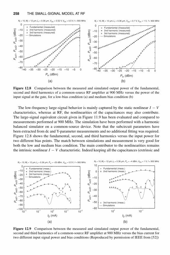
258 THE SMALL-SIGNAL MODEL AT RF
Fundamental (measured)2nd harmonic (measured)3rd harmonic (measured)Simulations
Pin (dBm)
–40 –35 –30 –25 –20 –15 –10 –5 0–80
–70
–60
–50
–40
–30
–20
–10
0
Po
ut1
, P
ou
t2, P
ou
t3 (
dB
m)
Nf = 10,Wf = 12 µm,Lf = 0.36 µm, VGS = 0.52 V,VDS = 0.5 V, f = 900 MHz
–40 –35 –30 –25 –20 –15 –10 –5 0–80
–70
–60
–50
–40
–30
–20
–10
0Fundamental (measured)2nd harmonic (measured)3rd harmonic (measured)Simulations
Pin (dBm)
Po
ut1
, P
ou
t2, P
ou
t3 (
dB
m)
Nf = 10,Wf = 12 µm,Lf = 0.36 µm, VGS = 0.7 V,VDS = 1 V, f = 900 MHz
(a) (b)
Figure 12.8 Comparison between the measured and simulated output power of the fundamental,
second and third harmonics of a common-source RF amplifier at 900 MHz versus the power of the
input signal at the gate, for a low-bias condition (a) and medium bias condition (b)
The low-frequency large-signal behavior is mainly captured by the static nonlinear I − V
characteristics, whereas at RF, the nonlinearities of the capacitances may also contribute.
The large-signal equivalent circuit given in Figure 11.9 has been evaluated and compared to
measurements performed at 900 MHz. The simulation have been performed with a harmonic
balanced simulator on a common-source device. Note that the subcircuit parameters have
been extracted from dc and Y-parameter measurements and no additional fitting was required.
Figure 12.8 shows the fundamental, second, and third harmonics versus the input power for
two different bias points. The match between simulations and measurement is very good for
both the low and medium bias condition. The main contributor to the nonlinearities remains
the intrinsic nonlinear I − V characteristic. Indeed keeping all the capacitances (extrinsic and
–100
–90
–80
–70
–60
–50
–40
–30
–20
–10
0
Po
ut1
, P
ou
t2, P
ou
t3 (
dB
m)
ID (mA)
10–2
10–1
100
10+1
10+2
Fundamental (meas.)2nd harmonic (meas.)3rd harmonic (meas.)Simulations
Nf = 10,Wf = 12 µm,Lf = 0.36 µm, Pin = –20 dBm, VDS = 0.5 V, f = 900 MHz
–60
–50
–40
–30
–20
–10
0
10
ID (mA)
100
10+1
Fundamental (meas.)2nd harmonic (meas.)
3rd harmonic (meas.)Simulations
Nf = 10,Wf = 12 µm,Lf = 0.36 µm, Pin = –4 dBm, VDS = 1 V, f = 900 MHz
Po
ut1
, P
ou
t2, P
ou
t3 (
dB
m)
(a) (b)
Figure 12.9 Comparison between the measured and simulated output power of the fundamental,
second and third harmonics of a common-source RF amplifier at 900 MHz versus the bias current for
two different input signal power and bias conditions (Reproduced by permission of IEEE from [52])
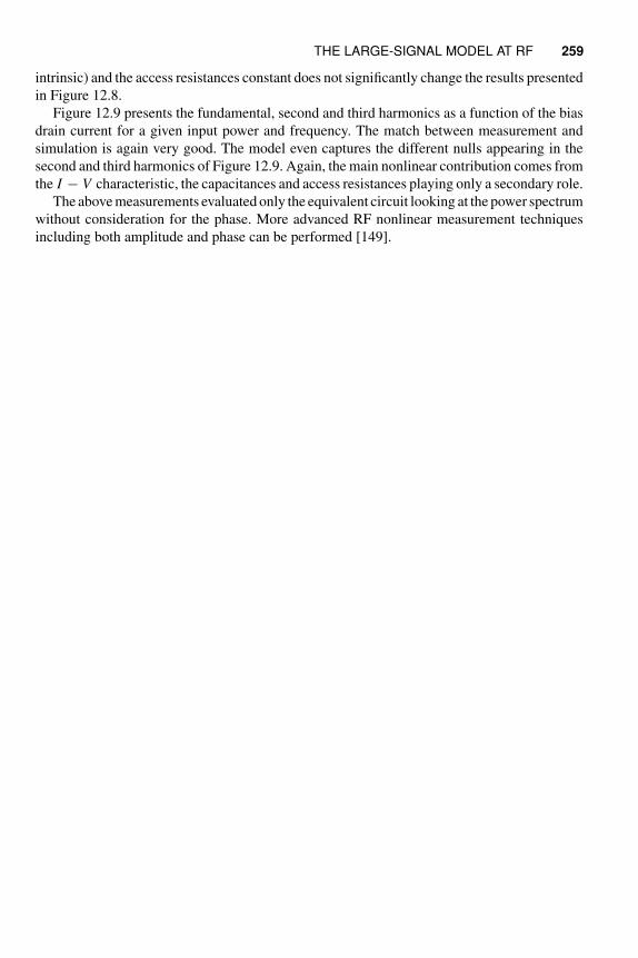
THE LARGE-SIGNAL MODEL AT RF 259
intrinsic) and the access resistances constant does not significantly change the results presented
in Figure 12.8.
Figure 12.9 presents the fundamental, second and third harmonics as a function of the bias
drain current for a given input power and frequency. The match between measurement and
simulation is again very good. The model even captures the different nulls appearing in the
second and third harmonics of Figure 12.9. Again, the main nonlinear contribution comes from
the I − V characteristic, the capacitances and access resistances playing only a secondary role.
The above measurements evaluated only the equivalent circuit looking at the power spectrum
without consideration for the phase. More advanced RF nonlinear measurement techniques
including both amplitude and phase can be performed [149].

13 The Noise Model at RF
The chapter starts with the theory of noisy two-port networks where it is shown that two noise
sources (for example, a series voltage source and a shunt current source at the input) as well as
their correlation admittance are required to fully characterize the noisy two-port. The important
definition of noise figure is introduced and it is shown that this noise figure can be minimized
by setting the source admittance to an appropriate value. It is shown that the noisy two-port
can be characterized by a total of four noise parameters, including the minimum noise figure,
the input-referred noise resistance, and the real and imaginary parts of the optimum source
admittance that minimize the noise figure. The noise model discussed in the previous chapters
was exclusively looking at the noise produced at the drain. At high frequency, the capacitive
coupling between the channel and the gate on one hand and between the channel and bulk on
the other hand induce noise currents to flow in the gate and bulk terminals in addition to the
noise produced at the source and drain. A complete non-quasi-static thermal noise model is
then presented in Section 13.2, where the induced gate and substrate noise and their correlation
to the drain noise are derived. The chapter ends with the noise analysis of a common-source
amplifier, deriving the four noise parameters with different levels of approximation.
13.1 THE HF NOISE PARAMETERS
13.1.1 The Noisy Two-Port
The noise at the output of an amplifier arises from the noise generated within the amplifier
plus the noise already present at the input and amplified by the amplifier. Such a small-signal
noisy amplifier can be represented by the noisy two-port network shown in Figure 13.1(a). The
output noise current Inout includes both the noise coming from the amplifier and the amplified
input noise. Note that we look at the short-circuited output noise current because we will
characterize the two-port using the Y-parameters which are defined in short-circuit conditions.
The noisy two-port of Figure 13.1(a) can be represented by a noiseless two-port to which two
noise sources have to be added (actually one noise source per port) [145, 146]. Figure 13.1(b)
shows one possible representation where two current noise sources have been added to the
Charge-Based MOS Transistor Modeling: The EKV Model for Low-Power and RF IC Design C. Enz and E. VittozC© 2006 John Wiley & Sons, Ltd.
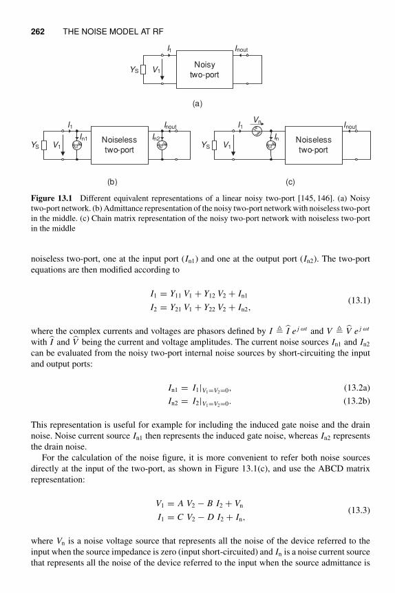
262 THE NOISE MODEL AT RF
I1
Noiseless
two-port
Inout
YS V1
In1 In2
I1
Noiseless
two-port
Inout
YS V1
In
Vn
I1
Noisy
two-port
Inout
YS V1
(a)
(b) (c)
Figure 13.1 Different equivalent representations of a linear noisy two-port [145, 146]. (a) Noisy
two-port network. (b) Admittance representation of the noisy two-port network with noiseless two-port
in the middle. (c) Chain matrix representation of the noisy two-port network with noiseless two-port
in the middle
noiseless two-port, one at the input port (In1) and one at the output port (In2). The two-port
equations are then modified according to
I1 = Y11 V1 + Y12 V2 + In1(13.1)
I2 = Y21 V1 + Y22 V2 + In2,
where the complex currents and voltages are phasors defined by I I e j ωt and V V e j ωt
with I and V being the current and voltage amplitudes. The current noise sources In1 and In2
can be evaluated from the noisy two-port internal noise sources by short-circuiting the input
and output ports:
In1 = I1|V1=V2=0, (13.2a)
In2 = I2|V1=V2=0. (13.2b)
This representation is useful for example for including the induced gate noise and the drain
noise. Noise current source In1 then represents the induced gate noise, whereas In2 represents
the drain noise.
For the calculation of the noise figure, it is more convenient to refer both noise sources
directly at the input of the two-port, as shown in Figure 13.1(c), and use the ABCD matrix
representation:
V1 = A V2 − B I2 + Vn(13.3)
I1 = C V2 − D I2 + In,
where Vn is a noise voltage source that represents all the noise of the device referred to the
input when the source impedance is zero (input short-circuited) and In is a noise current source
that represents all the noise of the device referred to the input when the source admittance is
THE HF NOISE PARAMETERS 263
zero (input open circuited):
Vn = B I2|V1=V2=0 = −1
Y21
I2|V1=V2=0, (13.4a)
In = D I2|I1=V2=0 = −Y11
Y21
I2|I1=V2=0. (13.4b)
Vn is calculated using (13.4a) by first evaluating the Y-parameters, calculating the output
current I2 with the input and output in short circuit, and dividing this value by −Y21. Similarly,
In is calculated by first evaluating the output current I2 with the input open and the output in
short circuit and multiplying this value by −Y11/Y21. Examples of Vn and In noise sources are
presented in Section 13.3.
The two noise sources Vn and In of Figure 13.1(c) are related to the noise sources In1 and
In2 of Figure 13.1(b) by
Vn = −In2
Y21
, (13.5a)
In = In1 −Y11
Y21
In2. (13.5b)
13.1.2 The Correlation Admittance
Since both of the noise sources Vn and In (or equivalently In1 and In2) are due to the same
physical noise sources within the two-port, they are usually correlated. To account for the
correlation existing between sources In and Vn, noise source In can be written as
In = Inu + Inc = Inu + Yc Vn, (13.6)
where Inu stands for the uncorrelated part of In, and Inc represents the part of In that is fully
correlated to Vn. The definition of the correlation admittance Yc is obtained by multiplying
(13.6) by V ∗n and averaging. This results in
InV ∗n = InuV ∗
n︸ ︷︷ ︸
=0
+Yc |Vn|2 = Yc |Vn|2, (13.7)
where the first term of the right-hand side of (13.7) is zero since by definition Inu is not
correlated to Vn. Yc is then given by
Yc =In V ∗
n
|Vn|2. (13.8)
The mean-square value of source In is given by
|In|2 = |Inu|2 + |Yc|2 |Vn|2 + Y ∗c Inu V ∗
n︸ ︷︷ ︸
=0
+ Yc Vn I ∗nu
︸ ︷︷ ︸
=0 (13.9)= |Inu|2 + |Yc|2 |Vn|2
︸ ︷︷ ︸
|Inc|2
.
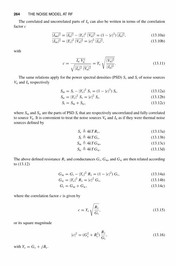
264 THE NOISE MODEL AT RF
The correlated and uncorrelated parts of In can also be written in terms of the correlation
factor c
|Inu|2 = |In|2 − |Yc|2 |Vn|2 = (1 − |c|2) |In|2, (13.10a)
|Inc|2 = |Yc|2 |Vn|2 = |c|2 |In|2, (13.10b)
with
c =In V ∗
n√
|In|2 |Vn|2= Yc
√
|Vn|2
|In|2. (13.11)
The same relations apply for the power spectral densities (PSD) Sv and Si of noise sources
Vn and In respectively
Siu = Si − |Yc|2 Sv = (1 − |c|2) Si, (13.12a)
Sic = |Yc|2 Sv = |c|2 Si, (13.12b)
Si = Siu + Sic, (13.12c)
where Siu and Sic are the parts of PSD Si that are respectively uncorrelated and fully correlated
to source Vn. It is convenient to treat the noise sources Vn and In as if they were thermal noise
sources defined by
Sv 4kT Rv, (13.13a)
Si 4kT G i, (13.13b)
Siu 4kT G iu, (13.13c)
Sic 4kT G ic. (13.13d)
The above defined resistance Rv and conductances G i, G iu, and G ic are then related according
to (13.12)
G iu = G i − |Yc|2 Rv = (1 − |c|2) G i, (13.14a)
G ic = |Yc|2 Rv = |c|2 G i, (13.14b)
G i = G iu + G ic, (13.14c)
where the correlation factor c is given by
c = Yc
√
Rv
G i
, (13.15)
or its square magnitude
|c|2 = (G2c + B2
c )Rv
G i
, (13.16)
with Yc = Gc + j Bc.
THE HF NOISE PARAMETERS 265
Note that in general Rv, G i, G iu, and G ic are frequency dependent since they depend on the
real physical noise sources within the two-port through the Y-parameters.
To be fully characterized, the noise of a two-port requires four noise parameters, for example,
Rv, G iu, Gc, and Bc. As will be shown in the next section, all these noise parameters are required
to evaluate the noise factor.
13.1.3 The Noise Factor
The noise factor is defined as the ratio of the total output noise to the output noise due only to
the noise already present at the two-port input:
F total output noise
output noise due to input source= 1 +
Na
Ns
, (13.17)
where Na is the noise power added by the two-port and Ns is the noise power coming from the
source. To calculate the noise factor of a two-port in terms of the equivalent noise sources Vn
and In and their correlation admittance, we first have to evaluate the total noise at the two-port
output. Since the current noise contribution coming from the source Inrs and that coming from
Vn and In are amplified the same way, we can just calculate the total noise current In tot in
short-circuit condition at the input of the two-port. With the help of Figure 13.2, the current
source In tot is given by
In tot = Inrs + In + Ys Vn, (13.18)
and the mean-square value is
|In tot|2 = |Inrs + In + Ys Vn|2 = |Inrs|2 + |In + Ys Vn|2, (13.19)
which can be rewritten in terms of correlated and uncorrelated noise as
|In tot|2 = |Inrs|2 + |Inu + Inc + Ys Vn|2
= |Inrs|2 + |Inu + (Yc + Ys) Vn|2 (13.20)
= |Inrs|2 + |Inu|2 + |Yc + Ys|2 |Vn|2.
The noise factor is then simply given by
F |In tot|2
|Inrs|2= 1 +
|Inu|2 + |Yc + Ys|2 |Vn|2
|Inrs|2. (13.21)
YS
In
Vn
Inrs
Intot
YS
Intot
Intot
Figure 13.2 Total equivalent noise at the input of a noisy two-port
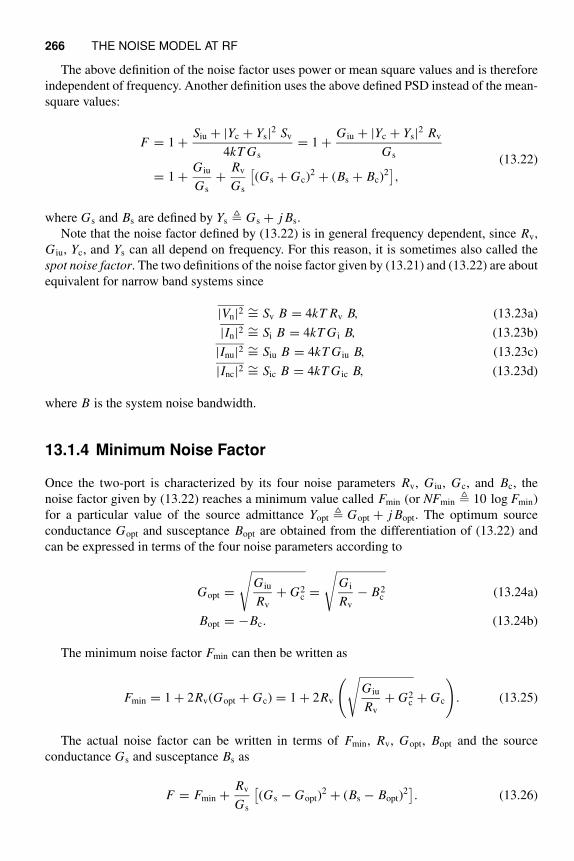
266 THE NOISE MODEL AT RF
The above definition of the noise factor uses power or mean square values and is therefore
independent of frequency. Another definition uses the above defined PSD instead of the mean-
square values:
F = 1 +Siu + |Yc + Ys|2 Sv
4kT Gs
= 1 +G iu + |Yc + Ys|2 Rv
Gs (13.22)
= 1 +G iu
Gs
+Rv
Gs
[
(Gs + Gc)2 + (Bs + Bc)2]
,
where Gs and Bs are defined by Ys Gs + j Bs.
Note that the noise factor defined by (13.22) is in general frequency dependent, since Rv,
G iu, Yc, and Ys can all depend on frequency. For this reason, it is sometimes also called the
spot noise factor. The two definitions of the noise factor given by (13.21) and (13.22) are about
equivalent for narrow band systems since
|Vn|2 ∼= Sv B = 4kT Rv B, (13.23a)
|In|2 ∼= Si B = 4kT G i B, (13.23b)
|Inu|2 ∼= Siu B = 4kT G iu B, (13.23c)
|Inc|2 ∼= Sic B = 4kT G ic B, (13.23d)
where B is the system noise bandwidth.
13.1.4 Minimum Noise Factor
Once the two-port is characterized by its four noise parameters Rv, G iu, Gc, and Bc, the
noise factor given by (13.22) reaches a minimum value called Fmin (or NFmin 10 log Fmin)
for a particular value of the source admittance Yopt Gopt + j Bopt. The optimum source
conductance Gopt and susceptance Bopt are obtained from the differentiation of (13.22) and
can be expressed in terms of the four noise parameters according to
Gopt =
√
G iu
Rv
+ G2c =
√
G i
Rv
− B2c (13.24a)
Bopt = −Bc. (13.24b)
The minimum noise factor Fmin can then be written as
Fmin = 1 + 2Rv(Gopt + Gc) = 1 + 2Rv
(
√
G iu
Rv
+ G2c + Gc
)
. (13.25)
The actual noise factor can be written in terms of Fmin, Rv, Gopt, Bopt and the source
conductance Gs and susceptance Bs as
F = Fmin +Rv
Gs
[
(Gs − Gopt)2 + (Bs − Bopt)
2]
. (13.26)
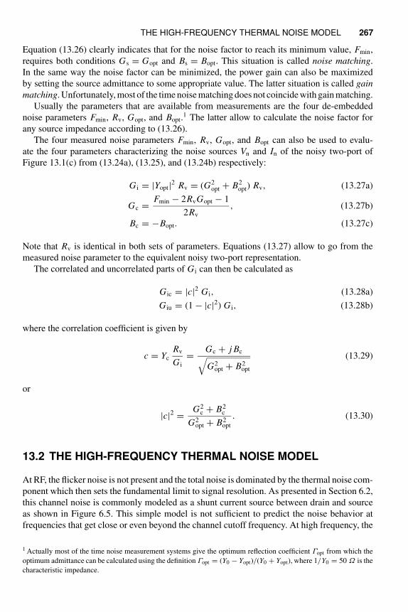
THE HIGH-FREQUENCY THERMAL NOISE MODEL 267
Equation (13.26) clearly indicates that for the noise factor to reach its minimum value, Fmin,
requires both conditions Gs = Gopt and Bs = Bopt. This situation is called noise matching.
In the same way the noise factor can be minimized, the power gain can also be maximized
by setting the source admittance to some appropriate value. The latter situation is called gain
matching. Unfortunately, most of the time noise matching does not coincide with gain matching.
Usually the parameters that are available from measurements are the four de-embedded
noise parameters Fmin, Rv, Gopt, and Bopt.1 The latter allow to calculate the noise factor for
any source impedance according to (13.26).
The four measured noise parameters Fmin, Rv, Gopt, and Bopt can also be used to evalu-
ate the four parameters characterizing the noise sources Vn and In of the noisy two-port of
Figure 13.1(c) from (13.24a), (13.25), and (13.24b) respectively:
G i = |Yopt|2 Rv = (G2opt + B2
opt) Rv, (13.27a)
Gc =Fmin − 2RvGopt − 1
2Rv
, (13.27b)
Bc = −Bopt. (13.27c)
Note that Rv is identical in both sets of parameters. Equations (13.27) allow to go from the
measured noise parameter to the equivalent noisy two-port representation.
The correlated and uncorrelated parts of G i can then be calculated as
G ic = |c|2 G i, (13.28a)
G iu = (1 − |c|2) G i, (13.28b)
where the correlation coefficient is given by
c = Yc
Rv
G i
=Gc + j Bc
√
G2opt + B2
opt
(13.29)
or
|c|2 =G2
c + B2c
G2opt + B2
opt
. (13.30)
13.2 THE HIGH-FREQUENCY THERMAL NOISE MODEL
At RF, the flicker noise is not present and the total noise is dominated by the thermal noise com-
ponent which then sets the fundamental limit to signal resolution. As presented in Section 6.2,
this channel noise is commonly modeled as a shunt current source between drain and source
as shown in Figure 6.5. This simple model is not sufficient to predict the noise behavior at
frequencies that get close or even beyond the channel cutoff frequency. At high frequency, the
1 Actually most of the time noise measurement systems give the optimum reflection coefficient Γopt from which the
optimum admittance can be calculated using the definition Γopt = (Y0 − Yopt)/(Y0 + Yopt), where 1/Y0 = 50 Ω is the
characteristic impedance.
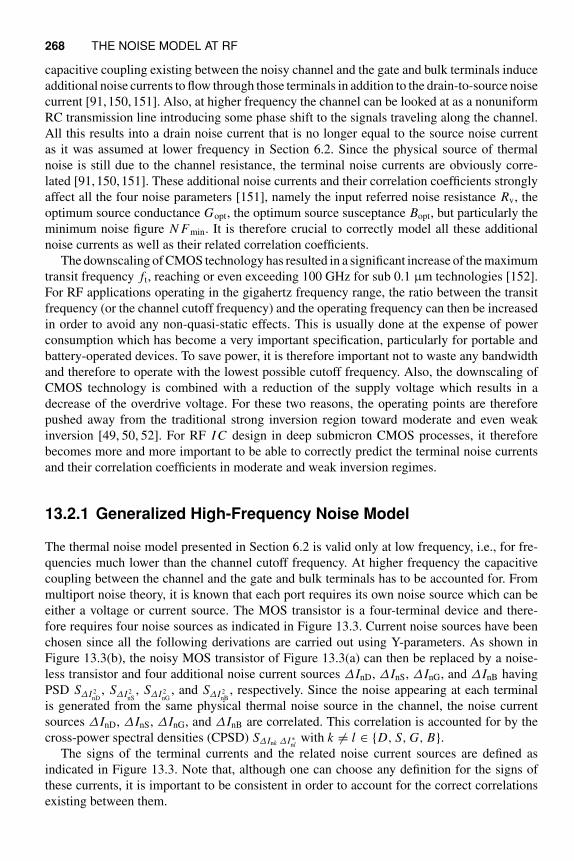
268 THE NOISE MODEL AT RF
capacitive coupling existing between the noisy channel and the gate and bulk terminals induce
additional noise currents to flow through those terminals in addition to the drain-to-source noise
current [91,150,151]. Also, at higher frequency the channel can be looked at as a nonuniform
RC transmission line introducing some phase shift to the signals traveling along the channel.
All this results into a drain noise current that is no longer equal to the source noise current
as it was assumed at lower frequency in Section 6.2. Since the physical source of thermal
noise is still due to the channel resistance, the terminal noise currents are obviously corre-
lated [91,150,151]. These additional noise currents and their correlation coefficients strongly
affect all the four noise parameters [151], namely the input referred noise resistance Rv, the
optimum source conductance Gopt, the optimum source susceptance Bopt, but particularly the
minimum noise figure N Fmin. It is therefore crucial to correctly model all these additional
noise currents as well as their related correlation coefficients.
The downscaling of CMOS technology has resulted in a significant increase of the maximum
transit frequency ft, reaching or even exceeding 100 GHz for sub 0.1 μm technologies [152].
For RF applications operating in the gigahertz frequency range, the ratio between the transit
frequency (or the channel cutoff frequency) and the operating frequency can then be increased
in order to avoid any non-quasi-static effects. This is usually done at the expense of power
consumption which has become a very important specification, particularly for portable and
battery-operated devices. To save power, it is therefore important not to waste any bandwidth
and therefore to operate with the lowest possible cutoff frequency. Also, the downscaling of
CMOS technology is combined with a reduction of the supply voltage which results in a
decrease of the overdrive voltage. For these two reasons, the operating points are therefore
pushed away from the traditional strong inversion region toward moderate and even weak
inversion [49, 50, 52]. For RF I C design in deep submicron CMOS processes, it therefore
becomes more and more important to be able to correctly predict the terminal noise currents
and their correlation coefficients in moderate and weak inversion regimes.
13.2.1 Generalized High-Frequency Noise Model
The thermal noise model presented in Section 6.2 is valid only at low frequency, i.e., for fre-
quencies much lower than the channel cutoff frequency. At higher frequency the capacitive
coupling between the channel and the gate and bulk terminals has to be accounted for. From
multiport noise theory, it is known that each port requires its own noise source which can be
either a voltage or current source. The MOS transistor is a four-terminal device and there-
fore requires four noise sources as indicated in Figure 13.3. Current noise sources have been
chosen since all the following derivations are carried out using Y-parameters. As shown in
Figure 13.3(b), the noisy MOS transistor of Figure 13.3(a) can then be replaced by a noise-
less transistor and four additional noise current sources ∆InD, ∆InS, ∆InG, and ∆InB having
PSD S∆I 2nD
, S∆I 2nS
, S∆I 2nG
, and S∆I 2nB
, respectively. Since the noise appearing at each terminal
is generated from the same physical thermal noise source in the channel, the noise current
sources ∆InD, ∆InS, ∆InG, and ∆InB are correlated. This correlation is accounted for by the
cross-power spectral densities (CPSD) S∆Ink ∆I ∗nl
with k = l ∈ D, S, G, B.The signs of the terminal currents and the related noise current sources are defined as
indicated in Figure 13.3. Note that, although one can choose any definition for the signs of
these currents, it is important to be consistent in order to account for the correct correlations
existing between them.
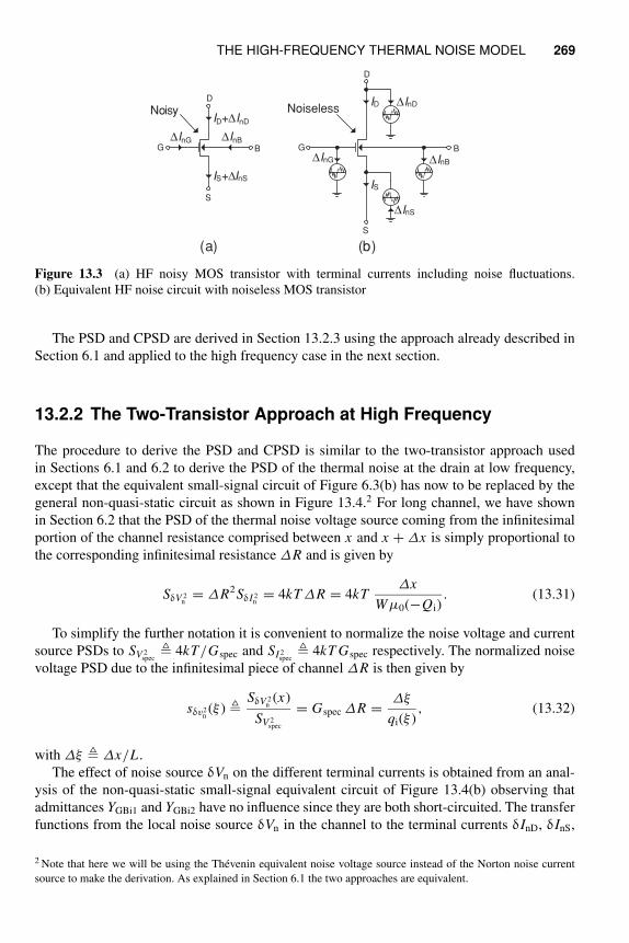
THE HIGH-FREQUENCY THERMAL NOISE MODEL 269
ID+∆InD
IS+∆InS
∆InG ∆InB
D
S
BG
ID
IS
D
S
BG
∆InD
∆InS
∆InB∆InG
Noisy Noiseless
(a) (b)
Figure 13.3 (a) HF noisy MOS transistor with terminal currents including noise fluctuations.
(b) Equivalent HF noise circuit with noiseless MOS transistor
The PSD and CPSD are derived in Section 13.2.3 using the approach already described in
Section 6.1 and applied to the high frequency case in the next section.
13.2.2 The Two-Transistor Approach at High Frequency
The procedure to derive the PSD and CPSD is similar to the two-transistor approach used
in Sections 6.1 and 6.2 to derive the PSD of the thermal noise at the drain at low frequency,
except that the equivalent small-signal circuit of Figure 6.3(b) has now to be replaced by the
general non-quasi-static circuit as shown in Figure 13.4.2 For long channel, we have shown
in Section 6.2 that the PSD of the thermal noise voltage source coming from the infinitesimal
portion of the channel resistance comprised between x and x + ∆x is simply proportional to
the corresponding infinitesimal resistance ∆R and is given by
SδV 2n
= ∆R2SδI 2n
= 4kT ∆R = 4kT∆x
Wµ0(−Qi). (13.31)
To simplify the further notation it is convenient to normalize the noise voltage and current
source PSDs to SV 2spec
4kT/Gspec and SI 2spec
4kT Gspec respectively. The normalized noise
voltage PSD due to the infinitesimal piece of channel ∆R is then given by
sδv2n(ξ )
SδV 2n(x)
SV 2spec
= Gspec ∆R =∆ξ
qi(ξ ), (13.32)
with ∆ξ ∆x/L .
The effect of noise source δVn on the different terminal currents is obtained from an anal-
ysis of the non-quasi-static small-signal equivalent circuit of Figure 13.4(b) observing that
admittances YGBi1 and YGBi2 have no influence since they are both short-circuited. The transfer
functions from the local noise source δVn in the channel to the terminal currents δInD, δInS,
2 Note that here we will be using the Thevenin equivalent noise voltage source instead of the Norton noise current
source to make the derivation. As explained in Section 6.1 the two approaches are equivalent.
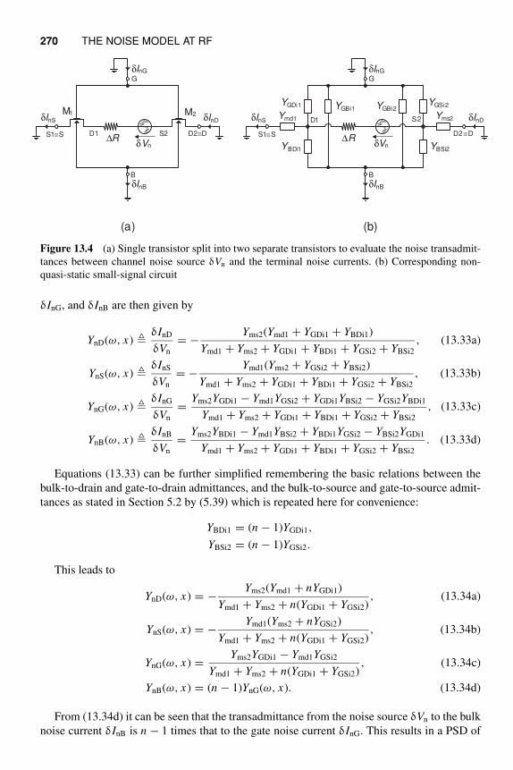
270 THE NOISE MODEL AT RF
M1
∆RδVn
M2
δInG
δInDδInS
δInB
S1≡S D1 S2
G
B
D2≡D ∆RδVn
δInG
δInDδInS
δInB
S1≡S
D1 S2
G
B
D2≡D
Ymd1
YGDi1
YBDi1
YGSi2
YBSi2
Yms2
(a) (b)
YGBi2YGBi1
Figure 13.4 (a) Single transistor split into two separate transistors to evaluate the noise transadmit-
tances between channel noise source δVn and the terminal noise currents. (b) Corresponding non-
quasi-static small-signal circuit
δInG, and δInB are then given by
YnD(ω, x) δInD
δVn
= −Yms2(Ymd1 + YGDi1 + YBDi1)
Ymd1 + Yms2 + YGDi1 + YBDi1 + YGSi2 + YBSi2
, (13.33a)
YnS(ω, x) δInS
δVn
= −Ymd1(Yms2 + YGSi2 + YBSi2)
Ymd1 + Yms2 + YGDi1 + YBDi1 + YGSi2 + YBSi2
, (13.33b)
YnG(ω, x) δInG
δVn
=Yms2YGDi1 − Ymd1YGSi2 + YGDi1YBSi2 − YGSi2YBDi1
Ymd1 + Yms2 + YGDi1 + YBDi1 + YGSi2 + YBSi2
, (13.33c)
YnB(ω, x) δInB
δVn
=Yms2YBDi1 − Ymd1YBSi2 + YBDi1YGSi2 − YBSi2YGDi1
Ymd1 + Yms2 + YGDi1 + YBDi1 + YGSi2 + YBSi2
. (13.33d)
Equations (13.33) can be further simplified remembering the basic relations between the
bulk-to-drain and gate-to-drain admittances, and the bulk-to-source and gate-to-source admit-
tances as stated in Section 5.2 by (5.39) which is repeated here for convenience:
YBDi1 = (n − 1)YGDi1,
YBSi2 = (n − 1)YGSi2.
This leads to
YnD(ω, x) = −Yms2(Ymd1 + nYGDi1)
Ymd1 + Yms2 + n(YGDi1 + YGSi2), (13.34a)
YnS(ω, x) = −Ymd1(Yms2 + nYGSi2)
Ymd1 + Yms2 + n(YGDi1 + YGSi2), (13.34b)
YnG(ω, x) =Yms2YGDi1 − Ymd1YGSi2
Ymd1 + Yms2 + n(YGDi1 + YGSi2), (13.34c)
YnB(ω, x) = (n − 1)YnG(ω, x). (13.34d)
From (13.34d) it can be seen that the transadmittance from the noise source δVn to the bulk
noise current δInB is n − 1 times that to the gate noise current δInG. This results in a PSD of
THE HIGH-FREQUENCY THERMAL NOISE MODEL 271
the induced bulk noise current δInB that is (n − 1)2 that of the induced gate noise current δInG:
SδI 2nB
= (n − 1)2 SδI 2nG
. (13.35)
Assuming a constant slope factor n, (13.35) is also valid for the total induced gate and bulk
currents ∆InG and ∆InB:
S∆I 2nB
= (n − 1)2 S∆I 2nG
. (13.36)
The noise transadmittances in (13.34) can be normalized by introducing the normalization
conductances of each half transistors M1 and M2 defined by [78, 153]
Gspec1 2nµ0
W
xCoxUT =
Gspec
ξ, (13.37a)
Gspec2 2nµ0
W
L − xCoxUT =
Gspec
1 − ξ, (13.37b)
and the frequency can be normalized using the specific frequency of each half transistors M1
and M2 defined as [78, 153]
ωspec1 µ0UT
x2=
ωspec
ξ 2, (13.38a)
ωspec2 µ0UT
(L − x)2=
ωspec
(1 − ξ )2, (13.38b)
with
ωspec µ0UT
L2(13.39)
being the specific frequency of the full-length transistor. Introducing the above normalizations
in (13.34) results in [78, 153]
ynD(Ω, ξ ) YnD
Gspec
(13.40a)
= −yms2(Ω(1 − ξ )2)[ymd1(Ωξ 2) + nyGDi1(Ωξ 2)]
(1 − ξ )ymd1(Ωξ 2) + ξ yms2(Ω(1 − ξ )2) + n[(1 − ξ )yGDi1(Ωξ 2) + ξ yGSi2(Ω(1 − ξ )2)],
ynS(Ω, ξ ) YnS
Gspec
(13.40b)
= −ymd1(Ωξ 2)[yms2(Ω(1 − ξ )2) + nyGSi2(Ω(1 − ξ )2)]
(1 − ξ )ymd1(Ωξ 2) + ξ yms2(Ω(1 − ξ )2) + n[(1 − ξ )yGDi1(Ωξ 2) + ξ yGSi2(Ω(1 − ξ )2)],
ynG(Ω, ξ ) YnG
Gspec
(13.40c)
=yms2(Ω(1 − ξ )2)yGDi1(Ωξ 2) − ymd1(Ωξ 2)yGSi2(Ω(1 − ξ )2)
(1 − ξ )ymd1(Ωξ 2) + ξ yms2(Ω(1 − ξ )2) + n[(1 − ξ )yGDi1(Ωξ 2) + ξ yGSi2(Ω(1 − ξ )2)],
ynB(Ω, ξ ) YnB
Gspec
= (n − 1)ynG(Ω, ξ ). (13.40d)
272 THE NOISE MODEL AT RF
where Ω ω/ωspec is the normalized frequency. The above noise transadmittances are then
used in the next section to derive the terminal noise current PSD and CPSD.
13.2.3 Generic PSDs Derivation
The PSD and CPSD of each noisy terminal currents due to the channel thermal noise voltage
source δVn are given by
SδI 2nk
(ω, x) = |Ynk(ω, x)|2 SδV 2n(x), (13.41a)
SδInkδI ∗nl
(ω, x) = Ynk(ω, x)Y ∗nl(ω, x) SδV 2
n(x), (13.41b)
with k = l ∈ D, S, G, B.Integrating these relations from source to drain and assuming that all noise sources in the
channel are uncorrelated, the following normalized relation can be derived [78, 153]:
s∆I 2nk
(Ω) S∆I 2
nk(ω)
SI 2spec
=∫ 1
0
|ynk(Ω, ξ )|2dξ
qi(ξ ), (13.42a)
s∆Ink∆I ∗nl
(Ω) S∆Ink∆I ∗
nl(ω)
SI 2spec
=∫ 1
0
ynk(Ω, ξ )y∗nl(Ω, ξ )
dξ
qi(ξ ). (13.42b)
At this point it is useful to introduce the following additional variables [78, 153]
χ (ξ ) qi(ξ ) +1
2, χs qs +
1
2, χd qd +
1
2, (13.43)
which greatly simplify the evaluation of the integrals in (13.42). Using these intermediate
variables, integrating the same current in the complete transistor and in transistors M1 and M2
leads to
id = χ2s − χ2
d , idξ = χ2s − χ2, id(1 − ξ ) = χ2 − χ2
d . (13.44)
Finally, the different normalized PSD and CPSD of (13.42) become [78, 153]
s∆I 2nk
(Ω) =1
id
∫ χs
χd
|ynk(Ω, χ )|24χ
2χ − 1dχ, (13.45a)
s∆Ink∆I ∗nl
(Ω) =1
id
∫ χs
χd
ynk(Ω, χ )y∗nl(Ω, χ )
4χ
2χ − 1dχ, (13.45b)
where variable ξ used in the expressions of the normalized transadmittances given by (13.40)
must also be expressed as a function of χ using the following relation:
ξ =χ2
s − χ2
id
. (13.46)
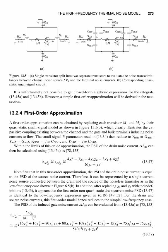
THE HIGH-FREQUENCY THERMAL NOISE MODEL 273
M1
∆R δVn
M2
δInG
δInDδInS
δInB
S1≡S D1 S2
G
B
D2≡D∆R δVn
δInG
δInDδInS
δInB
S1≡S
D1 S2
G
B
D2≡D
(a) (b)
Gmd1
CGDi1 CGSi2
CBDi1 CBSi2
Gms2
CGBi1 CGBi2
Figure 13.5 (a) Single transistor split into two separate transistors to evaluate the noise transadmit-
tances between channel noise source δVn and the terminal noise currents. (b) Corresponding quasi-
static small-signal circuit
It is unfortunately not possible to get closed-form algebraic expressions for the integrals
(13.45a) and (13.45b). However, a simple first-order approximation will be derived in the next
section.
13.2.4 First-Order Approximation
A first-order approximation can be obtained by replacing each transistor M1 and M2 by their
quasi-static small-signal model as shown in Figure 13.5(b), which clearly illustrates the ca-
pacitive coupling existing between the channel and the gate and bulk terminals inducing noise
currents to flow. The small-signal Y-parameters used in (13.34) then reduce to Ymd1 = Gmd1,
Yms2 = Gms2, YGDi1 = j ω CGDi1, and YGSi2 = j ω CGSi2.
Within the limits of this crude approximation, the PSD of the drain noise current ∆InD can
then be calculated using (13.45a) as [78, 153]
s∆i2nD
∼= s∆i2nS
∼=4χ2
s − 3χs + 4χsχd − 3χd + 4χ2d
6(χs + χd). (13.47)
Note first that in this first-order approximation, the PSD of the drain noise current is equal
to the PSD of the source noise current. Therefore, it can be represented by a single current
noise source connected between the drain and the source of the noiseless transistor as in the
low-frequency case shown in Figure 6.5(b). In addition, after replacing χs and χd with their def-
initions (13.43), it appears that the first-order non-quasi-static drain current noise PSD (13.47)
is identical to the low-frequency expression given in (6.19) [49, 52]. For the drain and
source noise currents, this first-order model hence reduces to the simple low-frequency case.
The PSD of the induced gate noise current ∆InG can be evaluated from (13.45a) as [78,153]
s∆i2nG
=s∆i2
nB
(n − 1)2
∼= Ω2 16χ4s + 16χ4
d + 80χ3s χd + 80χsχ
3d + 168χ2
s χ2d − 15χ3
s − 15χ3d − 75χ2
s χd − 75χsχ2d
540n2(χs + χd)5,
(13.48)
274 THE NOISE MODEL AT RF
gi
disi
YGi
(a) (b)
YGi
YGSi YGDi YGBi
gi
bi≡si≡di
Figure 13.6 Admittance seen at the gate of the intrinsic transistor
which is proportional to the square of the frequency. This is simply due to the capacitive
coupling existing between the channel and the gate. The bias dependence is a little bit more
complex than the PSD of the drain current noise. As mentioned above, the PSD of the in-
duced bulk noise current is simply (n − 1)2 that of the induced gate noise current given
by (13.48).
For VD = VS, the transistor is basically a passive resistor3 capacitively coupled to the gate
and the bulk. Hence, the Nyquist theorem applies and the induced gate noise for VD = VS
should therefore be equal to the noise of the conductance GGi ℜYGi seen at the gate. This
is no longer strictly true for VD = VS, but a thermal noise parameter at the gate δnG can be
defined as
δnG GnG
GGi
=s∆i2
nG
gGi
, (13.49)
where GnG is the thermal noise conductance at the gate defined by
S∆I 2nG
4kT GnG(ω) ∝ ω2. (13.50)
Similar to the definition of the thermal noise parameter at the drain, δnG measures the
deviation of the actual PSD of the induced gate noise current with respect to that of the
conductance GGi. With the quasi-static model, YGi is simply given by
YGi = j ω CGi = j ω (CGSi + CGDi + CGBi), (13.51)
which has no real component. Therefore a non-quasi-static approach is needed to evaluate the
real part of YGi. As shown in Figure 13.6, the gate sees the oxide capacitance in series with
part of the channel, which is responsible for the real part of YGi. The YGi admittance is simply
equal to the parallel connection of the intrinsic gate-to-source, gate-to-drain, and gate-to-bulk
admittances:
YGi = YGSi + YGDi + YGBi. (13.52)
3 Actually a resistor is always passive, but in this case, the term passive is used to emphasise the fact that for VD = VS
the transistor can be looked at as a passive RC network and the Nyquist and Bode theorems apply.
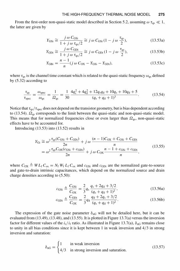
THE HIGH-FREQUENCY THERMAL NOISE MODEL 275
From the first-order non-quasi-static model described in Section 5.2, assuming ω τqs ≪ 1,
the latter are given by
YGSi∼=
j ω CGSi
1 + j ω τqs/2∼= j ω CGSi (1 − j ω
τqs
2), (13.53a)
YGDi∼=
j ω CGDi
1 + j ω τqs/2∼= j ω CGDi (1 − j ω
τqs
2), (13.53b)
YGBi =n − 1
n( j ω COX − YGSi − YGDi), (13.53c)
where τqs is the channel time constant which is related to the quasi-static frequency ωqs defined
by (5.32) according to
τqs
τspec
=ωspec
ωqs
=1
Ωqs
=1
30
4q2s + 4q2
d + 12qsqd + 10qs + 10qd + 5
(qs + qd + 1)3. (13.54)
Notice that τqs/τspec does not depend on the transistor geometry, but is bias dependent according
to (13.54). Ωqs corresponds to the limit between the quasi-static and non-quasi-static model.
This means that for normalized frequencies close or even larger than Ωqs, non-quasi-static
effects have to be accounted for.
Introducing (13.53) into (13.52) results in
YGi∼= ω2 τqs(CGSi + CGDi)
2n+ j ω
(n − 1)COX + CGSi + CGDi
n (13.55)
= ω2 τqsCOX(cGSi + cGDi)
2n+ j ω COX
n − 1 + cGSi + cGDi
n,
where COX W L f Cox = Nf Wf L f Cox and cGSi and cGDi are the normalized gate-to-source
and gate-to-drain intrinsic capacitances, which depend on the normalized source and drain
charge densities according to (5.50):
cGSi CGSi
COX
=2
3qs
qs + 2qd + 3/2
(qs + qd + 1)2, (13.56a)
cGDi CGDi
COX
=2
3qd
qd + 2qs + 3/2
(qs + qd + 1)2. (13.56b)
The expression of the gate noise parameter δnG will not be detailed here, but it can be
evaluated from (13.49), (13.48), and (13.55). It is plotted in Figure 13.7(a) versus the inversion
factor for different values of the ir/ if ratio. As illustrated in Figure 13.7(a), δnG remains close
to unity in all bias conditions since it is kept between 1 in weak inversion and 4/3 in strong
inversion and saturation:
δnG =
1 in weak inversion
4/3 in strong inversion and saturation.(13.57)
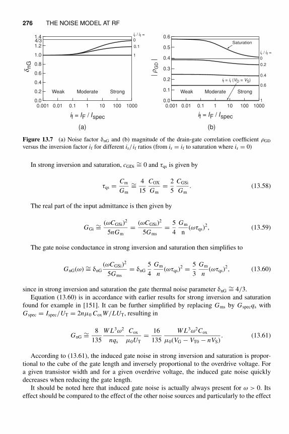
276 THE NOISE MODEL AT RF
1.4
1.2
1.0
0.8
0.6
0.4
0.2
0.0
d nG
0.001 0.01 0.1 1 10 100 1000
4/3
Weak Moderate Strong
0
0.1
1
0.6
0.5
0.4
0.3
0.2
0.1
0.0
| r
GD |
0.001 0.01 0.1 1 10 100 1000
if = IF / Ispec
Weak Moderate Strong
ir / i f =
0
1
0.2
0.4
0.6
Saturation
if = ir (VD = VS)
if = IF / Ispec
ir / i f =
(a) (b)
Figure 13.7 (a) Noise factor δnG and (b) magnitude of the drain-gate correlation coefficient ρGD
versus the inversion factor if for different ir/ if ratios (from ir = if to saturation where ir = 0)
In strong inversion and saturation, cGDi∼= 0 and τqs is given by
τqs =Cm
Gm
∼=4
15
COX
Gm
=2
5
CGSi
Gm
. (13.58)
The real part of the input admittance is then given by
GGi∼=
(ωCGSi)2
5nGm
=(ωCGSi)
2
5Gms
=5
4
Gm
n(ωτqs)
2, (13.59)
The gate noise conductance in strong inversion and saturation then simplifies to
GnG(ω) ∼= δnG
(ωCGSi)2
5Gms
= δnG
5
4
Gm
n(ωτqs)
2 =5
3
Gm
n(ωτqs)
2, (13.60)
since in strong inversion and saturation the gate thermal noise parameter δnG∼= 4/3.
Equation (13.60) is in accordance with earlier results for strong inversion and saturation
found for example in [151]. It can be further simplified by replacing Gms by Gspecqs with
Gspec = Ispec/UT = 2nµ0 CoxW/LUT, resulting in
GnG∼=
8
135
W L3ω2
nqs
Cox
µ0UT
=16
135
W L3ω2Cox
µ0(VG − VT0 − nVS). (13.61)
According to (13.61), the induced gate noise in strong inversion and saturation is propor-
tional to the cube of the gate length and inversely proportional to the overdrive voltage. For
a given transistor width and for a given overdrive voltage, the induced gate noise quickly
decreases when reducing the gate length.
It should be noted here that induced gate noise is actually always present for ω > 0. Its
effect should be compared to the effect of the other noise sources and particularly to the effect
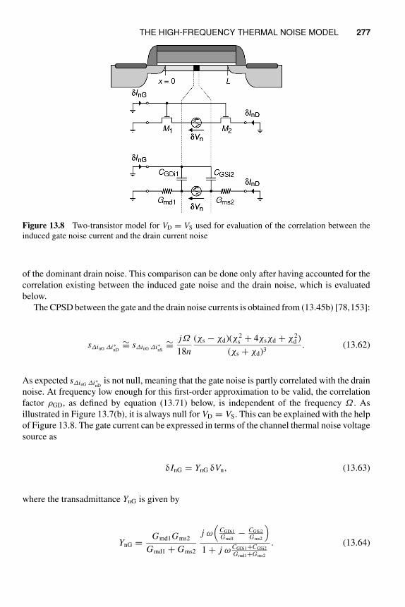
THE HIGH-FREQUENCY THERMAL NOISE MODEL 277
Figure 13.8 Two-transistor model for VD = VS used for evaluation of the correlation between the
induced gate noise current and the drain current noise
of the dominant drain noise. This comparison can be done only after having accounted for the
correlation existing between the induced gate noise and the drain noise, which is evaluated
below.
The CPSD between the gate and the drain noise currents is obtained from (13.45b) [78,153]:
s∆inG ∆i∗nD
∼= s∆inG ∆i∗nS
∼=jΩ
18n
(χs − χd)(χ2s + 4χsχd + χ2
d )
(χs + χd)3. (13.62)
As expected s∆inG ∆i∗nD
is not null, meaning that the gate noise is partly correlated with the drain
noise. At frequency low enough for this first-order approximation to be valid, the correlation
factor ρGD, as defined by equation (13.71) below, is independent of the frequency Ω . As
illustrated in Figure 13.7(b), it is always null for VD = VS. This can be explained with the help
of Figure 13.8. The gate current can be expressed in terms of the channel thermal noise voltage
source as
δInG = YnG δVn, (13.63)
where the transadmittance YnG is given by
YnG =Gmd1Gms2
Gmd1 + Gms2
j ω
(
CGDi1
Gmd1− CGSi2
Gms2
)
1 + j ω CGDi1+CGSi2
Gmd1+Gms2
. (13.64)
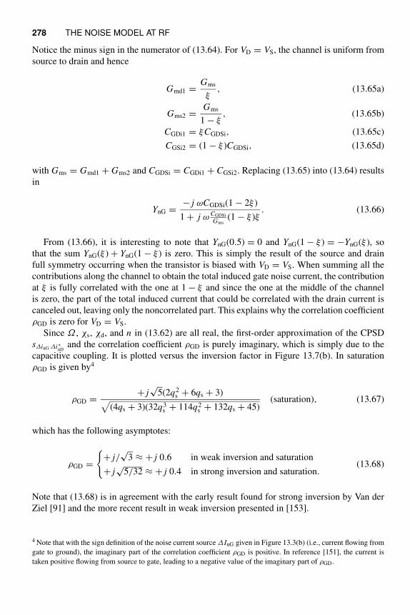
278 THE NOISE MODEL AT RF
Notice the minus sign in the numerator of (13.64). For VD = VS, the channel is uniform from
source to drain and hence
Gmd1 =Gms
ξ, (13.65a)
Gms2 =Gms
1 − ξ, (13.65b)
CGDi1 = ξCGDSi, (13.65c)
CGSi2 = (1 − ξ )CGDSi, (13.65d)
with Gms = Gmd1 + Gms2 and CGDSi = CGDi1 + CGSi2. Replacing (13.65) into (13.64) results
in
YnG =− j ωCGDSi(1 − 2ξ )
1 + j ω CGDSi
Gms(1 − ξ )ξ
. (13.66)
From (13.66), it is interesting to note that YnG(0.5) = 0 and YnG(1 − ξ ) = −YnG(ξ ), so
that the sum YnG(ξ ) + YnG(1 − ξ ) is zero. This is simply the result of the source and drain
full symmetry occurring when the transistor is biased with VD = VS. When summing all the
contributions along the channel to obtain the total induced gate noise current, the contribution
at ξ is fully correlated with the one at 1 − ξ and since the one at the middle of the channel
is zero, the part of the total induced current that could be correlated with the drain current is
canceled out, leaving only the noncorrelated part. This explains why the correlation coefficient
ρGD is zero for VD = VS.
Since Ω , χs, χd, and n in (13.62) are all real, the first-order approximation of the CPSD
s∆inG ∆i∗nD
and the correlation coefficient ρGD is purely imaginary, which is simply due to the
capacitive coupling. It is plotted versus the inversion factor in Figure 13.7(b). In saturation
ρGD is given by4
ρGD =+ j
√5(2q2
s + 6qs + 3)√
(4qs + 3)(32q3s + 114q2
s + 132qs + 45)(saturation), (13.67)
which has the following asymptotes:
ρGD =
+ j/√
3 ≈ + j 0.6 in weak inversion and saturation
+ j√
5/32 ≈ + j 0.4 in strong inversion and saturation.(13.68)
Note that (13.68) is in agreement with the early result found for strong inversion by Van der
Ziel [91] and the more recent result in weak inversion presented in [153].
4 Note that with the sign definition of the noise current source ∆InG given in Figure 13.3(b) (i.e., current flowing from
gate to ground), the imaginary part of the correlation coefficient ρGD is positive. In reference [151], the current is
taken positive flowing from source to gate, leading to a negative value of the imaginary part of ρGD.
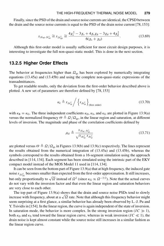
THE HIGH-FREQUENCY THERMAL NOISE MODEL 279
Finally, since the PSD of the drain and source noise currents are identical, the CPSD between
the drain and the source noise currents is equal to the PSD of the drain noise current [78,153]:
s∆inD ∆i∗nS
∼= s∆i2nD
∼=4χ2
s − 3χs + 4χsχd − 3χd + 4χ2d
6(χs + χd). (13.69)
Although this first-order model is usually sufficient for most circuit design purposes, it is
interesting to investigate the full non-quasi-static model. This is done in the next section.
13.2.5 Higher Order Effects
The behavior at frequencies higher than Ωqs has been explored by numerically integrating
equations (13.45a) and (13.45b) and using the complete non-quasi-static expressions of the
transadmittances.
To get readable results, only the deviation from the first-order behavior described above is
plotted. A new set of parameters are therefore defined by [78, 153]
κk s∆i2nk
/
s∆i2nk
(first order)(13.70)
with κB = κG. The three independent coefficients κD, κS, and κG are plotted in Figure 13.9(a)
versus the normalized frequency Θ Ω/Ωqs, in the linear region and saturation, at different
levels of inversion. The magnitude and phase of the correlation coefficients defined by
ρkl s∆ink ∆i∗
nl√
s∆i2nk
s∆i2nl
(13.71)
are plotted versus Θ Ω/Ωqs in Figures 13.9(b) and 13.9(c) respectively. The lines represent
the results obtained from the numerical integration of (13.45a) and (13.45b), whereas the
symbols correspond to the results obtained from a 16-segment simulation using the approach
described in [114, 134]. Each segment has been simulated using the intrinsic part of the EKV
compact model instead of the MOS Model 11 used in [114, 134].
It can be seen from the bottom part of Figure 13.9(a) that at high frequency, the induced gate
noise s∆I 2nG
becomes smaller than expected from the first-order approximation. It still increases,
but only proportionally to√
Ω instead of Ω2 (since κG ∝ Ω−3/2). Note that the actual curves
do not vary with the inversion factor and that even the linear region and saturation behaviors
are very close to each other.
The top part of Figure 13.9(a) shows that the drain and source noise PSDs tend to slowly
increase with frequency, about at a√
Ω rate. Note that although this frequency behavior might
seem surprising at a first glance, a similar behavior has already been observed by L.-J. Pu and
Y. Tsividis in [154]. In the linear region, the curve is again independent of the state of inversion.
In saturation mode, the behavior is more complex. In the strong inversion region (I C ≫ 1),
both κD and κS tend toward the linear region curve, whereas in weak inversion (I C ≪ 1), the
drain noise is kept almost constant while the source noise still increases in a similar fashion as
the linear region curve.
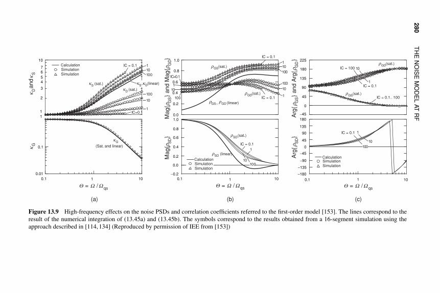
28
0T
HE
NO
ISE
MO
DE
LAT
RF
001
Simulation Simulation
1
01
1
01
Ma
gr
GS
an
d M
ag
rG
D
Ma
gr
SD
Arg
r G
S
an
d A
rgr
GD
A
rgr
SD
(linear)
(linear)
001
1.0=CI
001
011
01
1
1
01
001
101
001
kD
and k
S
Q = W / Wqs
kG
kS
(sat.)
kD
(sat.)
001
001
01
1
101
C = 0.1I
C = 0.1I
C = 0.1I
C = 0.1I
C=0.1I
κ ,S
(linear)
(Sat. and linear)
)a( )b( )c(
CalculationSimulationSimulation
kD
kG
Q = W / Wqs Q = W / W
qs
rGS
rGS
rGD
(sat.)
rGD
(sat.)
C = 0.1I
CalculationSimulationSimulation
rSD
rSD
(sat.)
Calculation
C = 100I
C = 0.1.. 100I
C = 0.1I
rGD
(sat.)
rGS
(sat.)2
1
1
0.1
0.1
0.01
10
76
54
3
1 10
1.0
0.8
0.6
0.4
0.2
0.0
1.0
0.8
0.6
0.4
0.2
0.0
0.1 10
−0.2
225
180
135
90
45
0
−45
180
135
90
45
0
−45
−90
−135
−180
0.1 11 10
,
Figure 13.9 High-frequency effects on the noise PSDs and correlation coefficients referred to the first-order model [153]. The lines correspond to the
result of the numerical integration of (13.45a) and (13.45b). The symbols correspond to the results obtained from a 16-segment simulation using the
approach described in [114, 134] (Reproduced by permission of IEE from [153])
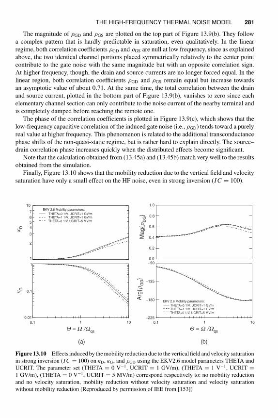
THE HIGH-FREQUENCY THERMAL NOISE MODEL 281
The magnitude of ρGD and ρGS are plotted on the top part of Figure 13.9(b). They follow
a complex pattern that is hardly predictable in saturation, even qualitatively. In the linear
regime, both correlation coefficients ρGD and ρGS are null at low frequency, since as explained
above, the two identical channel portions placed symmetrically relatively to the center point
contribute to the gate noise with the same magnitude but with an opposite correlation sign.
At higher frequency, though, the drain and source currents are no longer forced equal. In the
linear region, both correlation coefficients ρGD and ρGS remain equal but increase towards
an asymptotic value of about 0.71. At the same time, the total correlation between the drain
and source current, plotted in the bottom part of Figure 13.9(b), vanishes to zero since each
elementary channel section can only contribute to the noise current of the nearby terminal and
is completely damped before reaching the remote one.
The phase of the correlation coefficients is plotted in Figure 13.9(c), which shows that the
low-frequency capacitive correlation of the induced gate noise (i.e., ρGD) tends toward a purely
real value at higher frequency. This phenomenon is related to the additional transconductance
phase shifts of the non-quasi-static regime, but is rather hard to explain directly. The source–
drain correlation phase increases quickly when the distributed effects become significant.
Note that the calculation obtained from (13.45a) and (13.45b) match very well to the results
obtained from the simulation.
Finally, Figure 13.10 shows that the mobility reduction due to the vertical field and velocity
saturation have only a small effect on the HF noise, even in strong inversion (I C = 100).
2
3
4
5
6
7
10
1
1
0.1
0.01
0.1 1 110
kD
Q = W / Wqs
kG
(a)
Magr
DG
Q = W / Wqs
Arg
rG
D
(b)
EKV 2.6 Mobility parameters:
THETA=0 1/V, UCRIT=1 GV/mTHETA=1 1/V, UCRIT=1 GV/mTHETA=0 1/V, UCRIT=5 MV/m
THETA=0 1/V, UCRIT=1 GV/mTHETA=1 1/V, UCRIT=1 GV/mTHETA=0 1/V, UCRIT=5 MV/m
1.0
0.8
0.6
0.4
0.2
0.0−90
−135
−180
−2250.1 10
EKV 2.6 Mobility parameters:
Figure 13.10 Effects induced by the mobility reduction due to the vertical field and velocity saturation
in strong inversion (I C = 100) on κD, κG, and ρGD using the EKV2.6 model parameters THETA and
UCRIT. The parameter set (THETA = 0 V−1, UCRIT = 1 GV/m), (THETA = 1 V−1, UCRIT =1 GV/m), (THETA = 0 V−1, UCRIT = 5 MV/m) correspond respectively to: no mobility reduction
and no velocity saturation, mobility reduction without velocity saturation and velocity saturation
without mobility reduction (Reproduced by permission of IEE from [153])
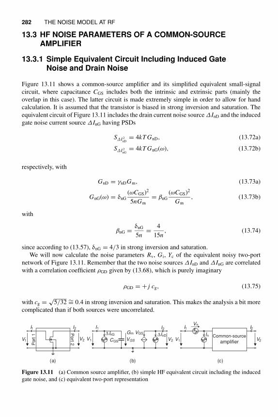
282 THE NOISE MODEL AT RF
13.3 HF NOISE PARAMETERS OF A COMMON-SOURCEAMPLIFIER
13.3.1 Simple Equivalent Circuit Including Induced GateNoise and Drain Noise
Figure 13.11 shows a common-source amplifier and its simplified equivalent small-signal
circuit, where capacitance CGS includes both the intrinsic and extrinsic parts (mainly the
overlap in this case). The latter circuit is made extremely simple in order to allow for hand
calculation. It is assumed that the transistor is biased in strong inversion and saturation. The
equivalent circuit of Figure 13.11 includes the drain current noise source ∆InD and the induced
gate noise current source ∆InG having PSDs
S∆I 2nD
= 4kT GnD, (13.72a)
S∆I 2nG
= 4kT GnG(ω), (13.72b)
respectively, with
GnD = γnDGm, (13.73a)
GnG(ω) = δnG
(ωCGS)2
5nGm
= βnG
(ωCGS)2
Gm
, (13.73b)
with
βnG =δnG
5n=
4
15n, (13.74)
since according to (13.57), δnG = 4/3 in strong inversion and saturation.
We will now calculate the noise parameters Rv, G i, Yc of the equivalent noisy two-port
network of Figure 13.11. Remember that the two noise sources ∆InD and ∆InG are correlated
with a correlation coefficient ρGD given by (13.68), which is purely imaginary
ρGD = + j cg, (13.75)
with cg =√
5/32 ∼= 0.4 in strong inversion and saturation. This makes the analysis a bit more
complicated than if both sources were uncorrelated.
I1 I2
V1 V2
Port
1
Po
rt 2
∆InG
I1
V1
Gm VGS ∆InD
I2
V2CGS
(a) (b)
I1
Common-source
amplifier
I2
V1
In
Vn
V2
(c)
VGS
Figure 13.11 (a) Common source amplifier, (b) simple HF equivalent circuit including the induced
gate noise, and (c) equivalent two-port representation
HF NOISE PARAMETERS OF A COMMON-SOURCE AMPLIFIER 283
We first have to calculate the noise sources Vn and In from their definitions given in (13.4)
which require the Y-parameters Y11 and Y21, which are easily calculated as
Y11 = j ω CGS, (13.76a)
Y21 = Gm. (13.76b)
The output current I2 when the input and output are short-circuited is given by
I2|V1=V2=0 = ∆InD, (13.77)
from which we obtain Vn as
Vn = −1
Y21
I2
∣
∣
V1=V2=0= −
∆InD
Gm
. (13.78)
The output current I2 when the input is open and the output is short-circuited is
I2
∣
∣
I1=V2=0= ∆InD −
Gm
j ω CGS
∆InG, (13.79)
from which we get In as
In = −Y11
Y21
I2
∣
∣
I1=V2=0= ∆InG −
j ω CGS
Gm
∆InD. (13.80)
The mean-square value of Vn is then given by
|Vn|2 =|∆InD|2
G2m
, (13.81)
whereas the mean-square value of In is given by
|In|2 = |∆InG|2 +(ω CGS
Gm
)2
|∆InD|2 +j ω CGS
Gm
(∆InG∆I ∗nD − ∆I ∗
nG∆InD). (13.82)
The mean-square values |∆InD|2 and |∆InG|2 can be expressed in terms of the PSDs S∆I 2nD
and S∆I 2nG
as
|∆InD|2 = S∆I 2nD
B = 4kT BGnD, (13.83a)
|∆InG|2 = S∆I 2nG
B = 4kT BGnG(ω), (13.83b)
where (13.72) have been used.
284 THE NOISE MODEL AT RF
For narrow-band systems, the definition of the correlation coefficient given by (13.71) can
be extended to the mean-square values as
ρkl s∆ink∆i∗
nl√
s∆i2nk
s∆i2nl
=∆Ink∆I ∗
nl√
|∆Ink |2|∆Inl |2. (13.84)
The mean-square values ∆InG∆I ∗nD and ∆I ∗
nG∆InD can then be expressed in terms of mean-
square values |∆InD|2 and |∆InG|2 and the correlation coefficient ρGD according to (13.84):
∆InG∆I ∗nD = ρGD
√
|∆InG|2|∆InD|2 = + jcg4kT B√
GnGGnD, (13.85a)
∆I ∗nG∆InD = ρ∗
GD
√
|∆InG|2|∆InD|2 = − jcg4kT B√
GnGGnD. (13.85b)
The noise parameters Rv and G i are then given by
Rv =|Vn|2
4kT B=
GnD
G2m
, (13.86a)
G i =|In|2
4kT B= GnG +
(ω CGS
Gm
)2
GnD −2cgω CGS
Gm
√
GnGGnD. (13.86b)
According to (13.8), for calculating Yc, we need InV ∗n which is given by
InV ∗n =
1
Gm
( j ω CGS
Gm
|∆InD|2 − ∆InG∆I ∗nD
)
(13.87)
=4kT B
Gm
( j ω CGS
Gm
GnD − jcg
√
GnGGnD
)
,
from which we get
Yc =InV ∗
n
|Vn|2= j
(
ω CGS − cgGm
√
GnG
GnD
)
. (13.88)
From (13.88), we see that Gc = 0 and Yc = j Bc.
Introducing the expressions of GnD and GnG given by (13.73) finally results in
Rv =γnD
Gm
, (13.89a)
G i = (ω CGS)2 γnD
Gm
(
1 +βnG
γnD
− 2cg
√
βnG
γnD
)
, (13.89b)
Gc = 0, (13.89c)
Bc = ω CGS
(
1 − cg
√
βnG
γnD
)
. (13.89d)
HF NOISE PARAMETERS OF A COMMON-SOURCE AMPLIFIER 285
The uncorrelated and correlated parts of G i are then obtained using (13.14):
G iu = (ω CGS)2 βnG
Gm
(1 − c2g), (13.90a)
G ic = (ω CGS)2 γnD
Gm
(
1 + c2g
βnG
γnD
− 2cg
√
βnG
γnD
)
. (13.90b)
From the Rv, G i, Yc parameters, we can derive the four noise parameters Rv, Gopt, Bopt, and
Fmin as a function of the circuit parameters using (13.24) and (13.25), resulting in
Gopt = ω CGS
√
βnG
γnD
(
1 − c2g
)
, (13.91a)
Bopt = −ω CGS
(
1 − cg
√
βnG
γnD
)
, (13.91b)
Fmin = 1 + 2ω CGS
γnD
Gm
√
βnG
γnD
(
1 − c2g
)
∼= 1 + 2γnD
ω
ωt
√
βnG
γnD
(
1 − c2g
)
, (13.91c)
where the Gm/CGS ratio has been approximated by the transit frequency ωt∼= Gm/CGS. Equa-
tions (13.91) reveal that, due to the induced gate noise, the noise matching condition is slightly
different than the gain matching condition which would require Bs = −ω CGS. Also, the min-
imum noise factor is strongly depending on the induced gate noise through parameters βnG
and cg. If induced gate noise was ignored (by setting βnG = 0), the minimum noise factor
would be equal to unity. This surprising result can be explained as follows: if the induced
gate noise is ignored, there is only the drain noise left and the optimum source conductance
is null whereas the optimum source susceptance is −ω CGS. This noise matching situation
corresponds to having an inductor with a susceptance value being −ω CGS and no internal
conductance. The input circuit is then an inductance in series with the transistor gate-to-source
capacitance. This source inductance will then resonate with the input transistor capacitance
at the operating frequency providing an infinite voltage gain at the input. The input referred
noise is then nulled, resulting in a unity noise factor.
Equation (13.91c) indicates that the minimum noise factor increases with frequency for a
given bias. For a given operating frequency, it can be decreased by increasing the transistor
transit frequency. This can be achieved by increasing the transistor bias or by reducing the
transistor length (or both). Technology scaling therefore leads to an improved noise factor at
a given frequency and bias.
It is also interesting to note that the correlation between the drain noise and the induced gate
noise reduces the noise factor compared to the situation where they would be fully uncorrelated.
Note that the above derivation has used the HF noise model which did not include short-
channel effects. As shown in Section 9.4, the noise parameter γnD is affected by effects such as
velocity saturation, carrier heating, mobility degradation due to the vertical field, and channel
length modulation. The HF noise model developed in Section 13.2 did not include these
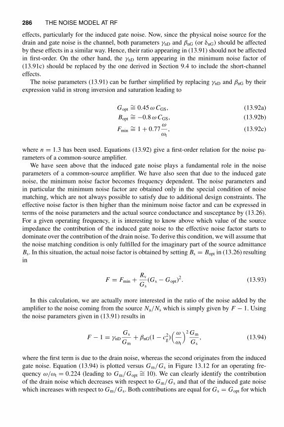
286 THE NOISE MODEL AT RF
effects, particularly for the induced gate noise. Now, since the physical noise source for the
drain and gate noise is the channel, both parameters γnD and βnG (or δnG) should be affected
by these effects in a similar way. Hence, their ratio appearing in (13.91) should not be affected
in first-order. On the other hand, the γnD term appearing in the minimum noise factor of
(13.91c) should be replaced by the one derived in Section 9.4 to include the short-channel
effects.
The noise parameters (13.91) can be further simplified by replacing γnD and βnG by their
expression valid in strong inversion and saturation leading to
Gopt∼= 0.45 ω CGS, (13.92a)
Bopt∼= −0.8 ω CGS, (13.92b)
Fmin∼= 1 + 0.77
ω
ωt
, (13.92c)
where n = 1.3 has been used. Equations (13.92) give a first-order relation for the noise pa-
rameters of a common-source amplifier.
We have seen above that the induced gate noise plays a fundamental role in the noise
parameters of a common-source amplifier. We have also seen that due to the induced gate
noise, the minimum noise factor becomes frequency dependent. The noise parameters and
in particular the minimum noise factor are obtained only in the special condition of noise
matching, which are not always possible to satisfy due to additional design constraints. The
effective noise factor is then higher than the minimum noise factor and can be expressed in
terms of the noise parameters and the actual source conductance and susceptance by (13.26).
For a given operating frequency, it is interesting to know above which value of the source
impedance the contribution of the induced gate noise to the effective noise factor starts to
dominate over the contribution of the drain noise. To derive this condition, we will assume that
the noise matching condition is only fulfilled for the imaginary part of the source admittance
Bs. In this situation, the actual noise factor is obtained by setting Bs = Bopt in (13.26) resulting
in
F = Fmin +Rv
Gs
(Gs − Gopt)2. (13.93)
In this calculation, we are actually more interested in the ratio of the noise added by the
amplifier to the noise coming from the source Na/Ns which is simply given by F − 1. Using
the noise parameters given in (13.91) results in
F − 1 = γnD
Gs
Gm
+ βnG(1 − c2g)
( ω
ωt
)2 Gm
Gs
, (13.94)
where the first term is due to the drain noise, whereas the second originates from the induced
gate noise. Equation (13.94) is plotted versus Gm/Gs in Figure 13.12 for an operating fre-
quency ω/ωt = 0.224 (leading to Gm/Gopt∼= 10). We can clearly identify the contribution
of the drain noise which decreases with respect to Gm/Gs and that of the induced gate noise
which increases with respect to Gm/Gs. Both contributions are equal for Gs = Gopt for which
HF NOISE PARAMETERS OF A COMMON-SOURCE AMPLIFIER 287
0.01
0.1
1
10
F −
1
0.1 1 10 100 1000
Gm / Gs
Gm
Gopt
Drain noiseGate
induced noise
Fmin − 1
w / w t = 0.224
n = 1.3
Figure 13.12 Noise added by the common-source amplifier normalized to the source noise versus
the source resistance normalized to the transistor transconductance for an operating frequency ω/ωt =0.224
F = Fmin. The drain noise dominates over the induced gate noise for Gm/Gs ≪ Gm/Gopt,
whereas the induced gate noise dominates over the drain noise for Gm/Gs ≫ Gm/Gopt. For
Gs = 1/50 Ω−1 and ω/ωt = 0.224, the transconductance needs to be larger than 200 mA/V
for the induced gate noise to dominate. This is a rather large transconductance and hence in
most practical cases, the Gm/Gs ratio is smaller than Gm/Gopt and therefore it is usually the
drain noise that actually dominates.
We can also find the frequency ωign at which the induced gate noise is equal to the drain
noise for a given source conductance Gs, by simply equating the first and the second term of
(13.94) and solving for ω. This results in
ωign
ωt
=√
γnD
βnG(1 − c2g)
Gs
Gm
∼=4
3
√
5
3n
Gs
Gm
∼= 2.24Gs
Gm
, (13.95)
where n = 1.3 has been used. We see from (13.95) that the frequency ωign at which the induced
gate noise contributes as much as the drain noise is a fraction of the transit frequency ωt which
is inversely proportional to the Gm/Gs ratio.
The above discussion somehow mitigates the importance of the induced gate noise in the
case of practical designs such as LNAs because the noise matching conditions are seldom
achieved due to other design constraints. Nevertheless, it remains an important contributor to
the minimum noise figure, which represents the ultimate noise figure that can be achieved by
a given device at a given frequency and for a given bias.
The previous analysis was based on a very simple small-signal equivalent circuit of a
common-source amplifier that considered only the drain noise and the induced gate noise.
Additional noise sources will be considered in the next section.
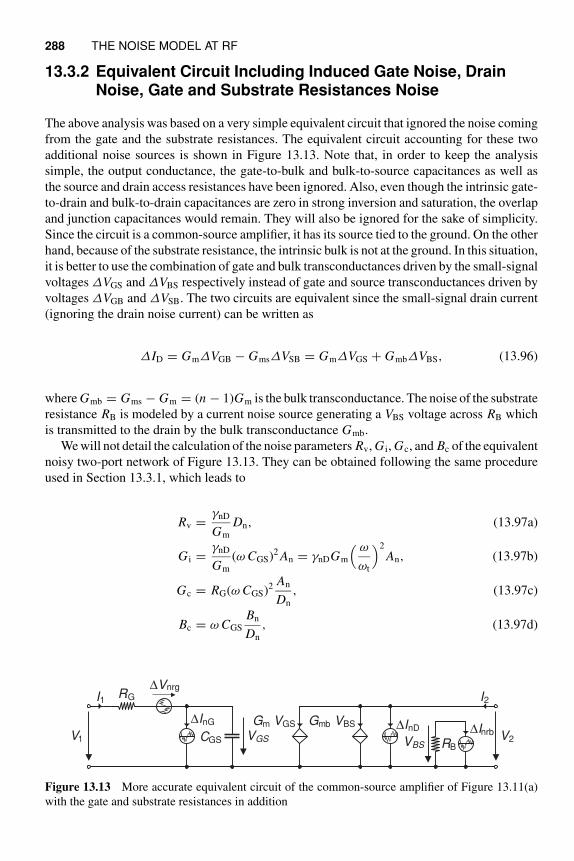
288 THE NOISE MODEL AT RF
13.3.2 Equivalent Circuit Including Induced Gate Noise, DrainNoise, Gate and Substrate Resistances Noise
The above analysis was based on a very simple equivalent circuit that ignored the noise coming
from the gate and the substrate resistances. The equivalent circuit accounting for these two
additional noise sources is shown in Figure 13.13. Note that, in order to keep the analysis
simple, the output conductance, the gate-to-bulk and bulk-to-source capacitances as well as
the source and drain access resistances have been ignored. Also, even though the intrinsic gate-
to-drain and bulk-to-drain capacitances are zero in strong inversion and saturation, the overlap
and junction capacitances would remain. They will also be ignored for the sake of simplicity.
Since the circuit is a common-source amplifier, it has its source tied to the ground. On the other
hand, because of the substrate resistance, the intrinsic bulk is not at the ground. In this situation,
it is better to use the combination of gate and bulk transconductances driven by the small-signal
voltages ∆VGS and ∆VBS respectively instead of gate and source transconductances driven by
voltages ∆VGB and ∆VSB. The two circuits are equivalent since the small-signal drain current
(ignoring the drain noise current) can be written as
∆ID = Gm∆VGB − Gms∆VSB = Gm∆VGS + Gmb∆VBS, (13.96)
where Gmb = Gms − Gm = (n − 1)Gm is the bulk transconductance. The noise of the substrate
resistance RB is modeled by a current noise source generating a VBS voltage across RB which
is transmitted to the drain by the bulk transconductance Gmb.
We will not detail the calculation of the noise parameters Rv, G i, Gc, and Bc of the equivalent
noisy two-port network of Figure 13.13. They can be obtained following the same procedure
used in Section 13.3.1, which leads to
Rv =γnD
Gm
Dn, (13.97a)
G i =γnD
Gm
(ω CGS)2 An = γnDGm
( ω
ωt
)2
An, (13.97b)
Gc = RG(ω CGS)2 An
Dn
, (13.97c)
Bc = ω CGS
Bn
Dn
, (13.97d)
VGS
∆InG
I1
V1
Gm VGS
VBS
∆InD
I2
V2CGS
RG
∆Vnrg
RB
∆InrbGmb VBS
Figure 13.13 More accurate equivalent circuit of the common-source amplifier of Figure 13.11(a)
with the gate and substrate resistances in addition
HF NOISE PARAMETERS OF A COMMON-SOURCE AMPLIFIER 289
where
Dn 1 + αB + αG + (RGω CGS)2 An
= 1 + αB + αG + (γnD αG)2( ω
ωt
)2
An, (13.98a)
An 1 + αB +βnG
γnD
− 2cg
√
βnG
γnD
, (13.98b)
Bn 1 + αB − cg
√
βnG
γnD
. (13.98c)
αG and αB are the thermal noise contributions of the gate and substrate resistances respectively,
normalized to the thermal noise of the drain:
αG Gm RG
γnD
, (13.99a)
αB G2
mb RB
γnDGm
=(n − 1)2
γnD
Gm RB. (13.99b)
The noise parameters Gopt, Bopt, and Fmin can then be calculated from Rv, G i, Gc, and Bc,
resulting in
Gopt = ω CGS
√
An Dn − B2n
Dn
, (13.100a)
Bopt = −ω CGS
Bn
Dn
, (13.100b)
Fmin = 1 + 2γnD
ω
ωt
√
An Dn − B2n + 2γ 2
nD αG
(
ω
ωt
)2
An
∼= 1 + 2γnD
ω
ωt
√
An Dn − B2n . (13.100c)
In a typical situation, the relative contributions of the gate and substrate resistances are
αG ≈5% and αB ≈ 20% [48,49,52]. Using values of parameters γnD, βnG, and cg given above
for strong inversion with n = 1.3 leads to An ≈ 1.1 and Bn ≈ 1. Assuming further that ω/ωt =0.1 allows to neglect the frequency-dependent part of Dn:
Dn∼= 1 + αB + αG
∼= 1.25. (13.101)
The four noise parameters can then be approximated by
Rv∼= 1.25
γnD
Gm
, (13.102a)
Gopt∼= 0.5 ω CGS, (13.102b)
Bopt∼= −0.8 ω CGS, (13.102c)
Fmin∼= 1 +
ω
ωt
. (13.102d)
290 THE NOISE MODEL AT RF
2.0
1.5
1.0
0.5
0.0
NF
min
(d
B)
0.50.40.30.20.1
w/w t
Nf = 10
Wf = 12 µm
Lf = 0.36 µm
Measurements
Simulation (with cg = 0)
Analytic Analytic (with cg = 0)
0.15
0.10
0.05
0.00
Go
pt
Z0
0.50.40.30.20.1
w/wt
VG = 0.743 V
VD = 1.5 V
ID = 1.116 mA
2.5
2.0
1.5
1.0
0.5
0.0
Rv / Z
0
0.50.40.30.20.1
w/w t
Gm = 10.7 mA/V
CGS = 129 fF
ft = 13.2 GHz
RG = 6.59 Ω
RB = 119 Ω
Z0 = 50 Ω
RG = RB = 0
−0.30
−0.25
−0.20
−0.15
−0.10
−0.05
0.00
Bo
pt
Z0
0.50.40.30.20.1
w/wt
Figure 13.14 Comparison between the measured, simulated, and the analytical results for the four
noise parameters
The noise parameters derived above are compared to those measured on an N-channel device
with Nf = 10, Wf = 12 μm, and L f = 0.36 μm biased in strong inversion and saturation. The
noise parameters have been carefully de-embedded using the methodology presented in [155].
They are plotted in Figure 13.14 and compared to the results obtained from simulation using the
complete subcircuit of Figure 11.9(c) with the additional induced gate noise source added to
the subcircuit (but not accounting for the correlation between induced gate noise and drain
thermal noise). Also, plotted in dashed lines in Figure 13.14 are the results obtained from
(13.102). The dashed-dotted line corresponds to (13.102) without accounting for the gate-to-
drain correlation ρGD by setting cg to zero. The discrepancies between the analytical and the
measured results mainly come from a wrong frequency behavior due to the extremely simple
equivalent circuit used for the analytical derivation. Nevertheless, the simple approximation
given by (13.102) already gives a reasonable estimation of the minimum noise figure and of
the other noise parameters.
References
1. Y. Tsividis, Operation and Modeling of the MOS Transistor, 2nd ed. New York: Mc-Graw-Hill,
1999.
2. M. Forrer, R. L. Coultre, A. Beyner, and H. Oguey, L’aventure de la montre a quartz. CH-2000
Neuchatel, Switzerland: Centredoc, 2002 (in French).
3. http://invention.smithsonian.org/centerpieces/quartz/inventors/swissinvent.html.
4. F. Leuenberger and E. Vittoz, “Complementary MOS Low-Power Low-Voltage Integrated Binary
Counter,” IEEE Proc., vol. 57, no. 9, pp. 1528–1532, Sept. 1969.
5. E. A. Vittoz, B. Gerber, and F. Leuenberger, “Silicon-Gate CMOS Frequency Divider for the
Electronic Wrist Watch,” IEEE J. Solid-State Circ., vol. 7, no. 2, pp. 100–104, Apr. 1972.
6. E. Vittoz and H. Oguey, “Complementary Dynamic Logic Circuits,” El. Lett., vol. 9, no. 4,
Jan. 1973.
7. H. Oguey and E. Vittoz, “CODYMOS Frequency Dividers Achieve Low Power Consumption and
High Frequency,” El. Lett., vol. 9, no. 17, Aug. 1973.
8. M. B. Barron, “Low Level Currents in Insulated Gate Field Effect Transistors,” Solid-State Elec-
tron., vol. 15, pp. 293–302, 1972.
9. R. M. Swanson and J. D. Meindl, “Ion-Implanted Complementary MOS Transistors in Low-Voltage
Circuits,” IEEE J. Solid-State Circ., vol. 7, no. 2, pp. 146–153, Apr. 1972.
10. R. R. Troutman and S. T. Chakravarti, “Subthreshold Characteristics of Insulated-Gate Field-Effect
Transistors,” IEEE Trans. Circ. Theory, vol. 20, no. 6, pp. 659–665, Nov. 1973.
11. T. Masuhara, J. Etoh, and M. Nagata, “A Precise MOSFET Model for Low-Voltage Circuits,” IEEE
Trans. Electron. Devices, vol. 21, no. 6, pp. 363–371, June 1974.
12. E. Vittoz and J. Fellrath, “New Analog CMOS IC’s Based on Weak Inversion Operation,” in
European Solid State Circ. Conf. Dig. Tech. Pap., Toulouse, pp. 12–13, Sept. 1976.
13. E. Vittoz and J. Fellrath, “CMOS Analog Integrated Circuits Based on Weak Inversion Operation,”
IEEE J. Solid State Circ., vol. 12, no. 3, pp. 224–231, June 1977.
14. J. Fellrath and E. Vittoz, “Small Signal Model of MOS Transistors in Weak Inversion,” in Proc.
Journees d’Electronique ’77, EPF-Lausanne, pp. 315–324, 1977.
15. P. G. A. Jespers, C. Jusseret, and Y. Leduc, “A Fast Sample and Hold Charge-Sensing Circuit for
Photodiode Arrays,” IEEE J. Solid-State Circ., vol. 12, no. 3, pp. 232–237, June 1977.
16. H. Wallinga and K. Bult, “Design and Analysis of CMOS Analog Processing Circuits by Means
of a Graphical MOST Model,” IEEE J. Solid-State Circ., vol. 24, no. 3, pp. 672–680, June 1989.
17. J.-D. Chatelain, Dispositifs a Semiconducteur, 2nd ed. ser. Traite d’Electricite. Editions Georgi,
1979, vol. 7.
Charge-Based MOS Transistor Modeling: The EKV Model for Low-Power and RF IC Design C. Enz and E. VittozC© 2006 John Wiley & Sons, Ltd.
292 REFERENCES
18. J. J. Ebers and J. L. Moll, “Large-Signal Behavior of Junction Transistors,” Proc. IRE, vol. 42,
no. 12, pp. 1761–1772, Dec. 1954.
19. H. Oguey and S. Cserveny, “Modele du transistor MOS valable dans un grand domaine de courants,”
Bulletin ASE, vol. 73, no. 3, pp. 113–116, 1982 (in French).
20. H. Oguey and S. Cserveny, “MOS Modelling at Low Current Density,” ESAT, Summer Course on
Process and Device Modelling, June 1983.
21. C. C. Enz, “High Precision CMOS Micropower Amplifiers,” Ph.D. Thesis, Swiss Federal Institute
of Technology, Thesis No. 802, 1989.
22. E. Vittoz, “Micropower Techniques,” in Design of MOS VLSI Circuits for Telecommunications,
Y. Tsividis and P. Antognetti, Eds. New Jersey: Prentice-Hall, 1985.
23. E. Vittoz, “Micropower Techniques,” in Design of Analog-Digital VLSI Circuits for Telecommuni-
cations and Signal Processing, J. Franca and Y. Tsividis, Eds. New Jersey: Prentice-Hall, 1994.
24. E. Vittoz, “MOS Transistor,” EPFL, Technical Report, 1988.
25. C. C. Enz, F. Krummenacher, and E. A. Vittoz, “An Analytical MOS Transistor Model Valid in
All Regions of Operation and Dedicated to Low-Voltage and Low-Current Applications,” Analog
Integr. Circ. Signal Process. J. Low-Voltage and Low-Power Des., vol. 8, pp. 83–114, July 1995.
26. M. Bagheri and C.Turchetti, “The Need for an Explicit Model Describing MOS Transistors in
Moderate Inversion.” El. Lett., vol. 21, no. 19, pp. 873–874, 1985.
27. M. A. Maher and C. A. Mead, “A Physical Charge-Conrolled Model for the MOS Transistors,”
in Advanced Research in VLSI, Proceeding of the 1987 Stanford Conference, P. Losleben, Ed.
Cambridge, MA: MIT Press, 1987.
28. M. A. Maher and C. Mead, “Fine Points of Transistor Physics,” in Analog VLSI and Neural Systems.
Addison-Wesley, 1989.
29. B. Iniguez and E. G. Moreno, “A Physically Based C∞-Continuous Model for Small-Geometry
MOSFET’s,” IEEE Trans. Electron. Devices, vol. 42, no. 2, pp. 283–287, Feb. 1995.
30. B. Iniguez and E. G. Moreno, “C∞-Continuous Small-Geometry MOSFET Modeling for Analog
Applications,” in Proc. 38th Midwest Symp. Circ. and Syst., pp. 41–44, Aug. 1995.
31. A. I. A. Cunha, S. M. Acosta, M. C. Schneider, and C. Galup-Montoro, “An Explicit MOSEFT
Model for Analog Circuit Simulation,” in Proc. IEEE Int. Symp. Circ. Syst., pp. 1592–1595, May
1995.
32. A. I. A. Cunha, M. C. Schneider, and C. Galup-Montoro, “An Explicit Physical Model for Long-
Channel MOS Transistor Including Small-Signal Parameters,” Solid-State Electron., vol. 38, no. 11,
pp. 1945–1952, 1995.
33. A. I. A. Cunha, O. C. Gouveia-Filho, M. C. Schneider, and C. Galup-Montoro, “A Current-Based
Model for the MOS Transistor,” in Proc. IEEE Int. Symp. Circ. Syst., pp. 1608–1611, June 1995.
34. A. I. A. Cunha, M. C. Schneider, and C. Galup-Montoro, “An MOS Transistor Model for Analog
Circuit Design,” IEEE J. Solid-State Circ., vol. 33, no. 10, pp. 1510–1519, Oct. 1998.
35. M. Bucher, C. Lallement, C. Enz, F. Theodoloz, and F. Krummenacher, “Scalable Gm/I Based
MOSFET Model,” in Proc. Int. Semiconductor Device Res. Symp., Charlottesville, Dec. 1997.
36. M. Bucher, J.-M. Sallese, C. Lallement, W. Grabinski, C. C. Enz, and F. Krummenacher, “Extended
Charges Modeling for Deep Submicron CMOS,” in Proc. Int. Semiconductor Device Res. Symp.,
Charlottesville, pp. 397–400, Dec. 1999.
37. M. Bucher, “Analytical MOS Transistor Modelling for Analog Circuit Simulation,” Ph.D. Thesis,
Swiss Federal Institute of Technology, Thesis No. 2114, 1999.
38. J.-M. Sallese and A.-S. Porret, “A Novel Approach to Charge Based Non Quasi Static Model of the
MOS Transistor Valid in all Modes of Operation,” Solid-State Electron., vol. 44, no. 6, pp. 887–894,
June 2000.
39. H. K. Gummel and K. Singhal, “Inversion Charge Modeling,” IEEE Trans. Electron. Devices,
vol. 48, no. 8, pp. 1585–1593, Aug. 2001.
40. H. K. Gummel and K. Singhal, “Intrinsic MOSFET Capacitance Coefficients,” IEEE Trans. Elec-
tron. Devices, vol. 48, no. 10, pp. 2384–2393, Oct. 2001.
REFERENCES 293
41. J.-M. Sallese, M. Bucher, F. Krummenacher, and P. Fazan, “Inversion Charge Linearization in
MOSFET Modeling and Rigourous Derivation of the EKV Compact Model,” Solid-State Electron.,
vol. 47, pp. 677–683, 2003.
42. C. Lallement, M. Bucher, and C. C. Enz, “Simple Solution for Modeling the Non-Uniform Substrate
Doping,” in Proc. IEEE Int. Symp. Circ. Syst., pp. 436–439, May 1996.
43. C. Lallement, M. Bucher, and C. C. Enz, “Modelling and Characterization of Non-Uniform Sub-
strate Doping,” Solid-State Electronics, vol. 41, no. 12, pp. 1857–1861, Dec. 1997.
44. A.-S. Porret, J.-M. Sallese, and C. C. Enz, “A Compact Non-Quasi-Static Extension of a Charge-
Based MOS Model,” IEEE Trans. Electron. Devices, vol. 48, no. 8, pp. 1647–1654, Aug. 2001.
45. J.-M. Sallese, M. Bucher, and C. Lallement, “Improved Analytical Modeling of Polysilicon Deple-
tion in MOSFETs for Circuit Simulation,” Solid-State Electron., vol. 44, no. 6, pp. 905–912, June
2000.
46. M. Bucher, J.-M. Sallese, and C. Lallement, “Accounting for Quantum Effects and Polysilicon
Depletion in an Analytical Design-Oriented MOSFET Model,” in Simulation of Semiconductor
Processes and Devices, C. T. D. Tsoukalas, Ed. Springer, 2001, pp. 296–299.
47. C. Lallement, J.-M. Sallese, M. Bucher, W. Grabinski, and P. C. Fazan, “Accounting for Quantum
Effects and Polysilicon Depletion From Weak to Strong Inversion in a Charge-Based Design-
Oriented MOSFET Model,” IEEE Trans. Electron. Devices, vol. 50, no. 2, pp. 406–417, Feb.
2003.
48. C. Enz and Y. Cheng, “MOS Transistor Modeling Issues for RF Circuit Design,” in Advances in
Analog Circuit Design (AACD’99), W. Sansen, J. Huijsing, and R. v. d. Plassche, Eds. Kluwer
Book, 1999, with Kind Permission of Springer Science and Business Media.
49. C. Enz and Y. Cheng, “MOS Transistor Modeling for RF IC Design,” IEEE J. Solid-State Circ.,
vol. 35, no. 2, pp. 186–201, c© 2000 IEEE.
50. C. Enz, “MOS Transistor Modeling for RF Integrated Circuit Design,” in Proc. IEEE Custom Integr.
Circ. Conf., pp. 189–196, May 2000.
51. C. Enz, “MOS Transistor Modeling for RF IC Design,” in Proc. Gallium Arsenide Semiconductor
Appl. Symp. (GAAS 2000), pp. 536–539, Oct. 2000.
52. C. Enz, “An MOS Transistor Model for RF IC Design Valid in All Regions of Operation,” IEEE
Trans. Microw. Theory Tech., vol. 50, no. 1, pp. 342–359, c© 2002 IEEE.
53. A. S. Roy and C. C. Enz, “Compact Modeling of Thermal Noise in the MOS Transistor,” in Proc.
11th Int. Conf. Mixed Des. Integr. Circ. and Syst. (MIXDES), Szczecin, Poland, pp. 71–78, June
2004.
54. A. S. Roy and C. C. Enz, “Compact Modeling of Thermal Noise in the MOS Transistor,” IEEE
Trans. Electron. Devices, vol. 52, no. 4, pp. 611–614, Apr. 2005.
55. A. S. Roy and C. C. Enz, “An Analytical Thermal Noise Model of the MOS Transistor Valid in All
Modes of Operation,” in Int. Conf. Noise and Fluctuations, Sept. 2005.
56. F. Pregaldiny, C. Lallement, and D. Mathiot, “A Simple Efficient Model of Parasitic Capacitances of
Deep-Submicron LDD MOSFETs,” Solid-State Electron., vol. 46, no. 12, pp. 2191–2198, copyright
2002.
57. M. Bucher, C. C. Enz, F. Krummenacher, J.-M. Sallese, C. Lallement, and A.-S. Porret, “The EKV
3.0 Compact MOS Transistor Model: Accounting for Deep-Submicron Aspects,” in Workshop
Compact Model. Int. Conf. Model. Simul. Microsyst., Puerto Rico, pp. 670–673, Apr. 2002.
58. M. Bucher, J.-M. Sallese, F. Krummenacher, D. Kazazis, C. Lallement, W. Grabinski, and C. Enz,
“EKV 3.0: An Analog Design-Oriented MOS Transistor Model,” in Proc. 9th Int. Conf. Mixed
Des. Integr. Circ. Syst. (MIXDES), Wroclaw, Poland, June 20–22, 2002.
59. G. Machado, C. C. Enz, and M. Bucher, “Estimating Key Parameters in the EKV MOST Model
for Analogue Design and Simulation,” in Proc. IEEE Int. Symp. Circuits Syst., pp. 1588–1591,
May 1995.
60. M. Bucher, C. Lallement, and C. C. Enz, “An Efficient Parameter Extraction Methodology for the
EKV MOST Model,” in Proc. IEEE Int. Conf. Microelectron. Test Struct., pp. 145–150, Mar. 1996.
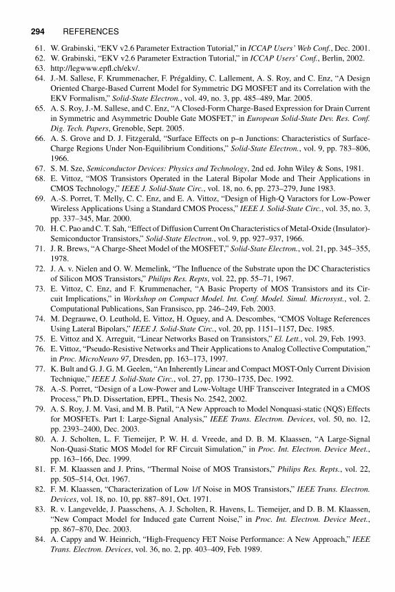
294 REFERENCES
61. W. Grabinski, “EKV v2.6 Parameter Extraction Tutorial,” in ICCAP Users’ Web Conf., Dec. 2001.
62. W. Grabinski, “EKV v2.6 Parameter Extraction Tutorial,” in ICCAP Users’ Conf., Berlin, 2002.
63. http://legwww.epfl.ch/ekv/.
64. J.-M. Sallese, F. Krummenacher, F. Pregaldiny, C. Lallement, A. S. Roy, and C. Enz, “A Design
Oriented Charge-Based Current Model for Symmetric DG MOSFET and its Correlation with the
EKV Formalism,” Solid-State Electron., vol. 49, no. 3, pp. 485–489, Mar. 2005.
65. A. S. Roy, J.-M. Sallese, and C. Enz, “A Closed-Form Charge-Based Expression for Drain Current
in Symmetric and Asymmetric Double Gate MOSFET,” in European Solid-State Dev. Res. Conf.
Dig. Tech. Papers, Grenoble, Sept. 2005.
66. A. S. Grove and D. J. Fitzgerald, “Surface Effects on p–n Junctions: Characteristics of Surface-
Charge Regions Under Non-Equilibrium Conditions,” Solid-State Electron., vol. 9, pp. 783–806,
1966.
67. S. M. Sze, Semiconductor Devices: Physics and Technology, 2nd ed. John Wiley & Sons, 1981.
68. E. Vittoz, “MOS Transistors Operated in the Lateral Bipolar Mode and Their Applications in
CMOS Technology,” IEEE J. Solid-State Circ., vol. 18, no. 6, pp. 273–279, June 1983.
69. A.-S. Porret, T. Melly, C. C. Enz, and E. A. Vittoz, “Design of High-Q Varactors for Low-Power
Wireless Applications Using a Standard CMOS Process,” IEEE J. Solid-State Circ., vol. 35, no. 3,
pp. 337–345, Mar. 2000.
70. H. C. Pao and C. T. Sah, “Effect of Diffusion Current On Characteristics of Metal-Oxide (Insulator)-
Semiconductor Transistors,” Solid-State Electron., vol. 9, pp. 927–937, 1966.
71. J. R. Brews, “A Charge-Sheet Model of the MOSFET,” Solid-State Electron., vol. 21, pp. 345–355,
1978.
72. J. A. v. Nielen and O. W. Memelink, “The Influence of the Substrate upon the DC Characteristics
of Silicon MOS Transistors,” Philips Res. Repts, vol. 22, pp. 55–71, 1967.
73. E. Vittoz, C. Enz, and F. Krummenacher, “A Basic Property of MOS Transistors and its Cir-
cuit Implications,” in Workshop on Compact Model. Int. Conf. Model. Simul. Microsyst., vol. 2.
Computational Publications, San Fransisco, pp. 246–249, Feb. 2003.
74. M. Degrauwe, O. Leuthold, E. Vittoz, H. Oguey, and A. Descombes, “CMOS Voltage References
Using Lateral Bipolars,” IEEE J. Solid-State Circ., vol. 20, pp. 1151–1157, Dec. 1985.
75. E. Vittoz and X. Arreguit, “Linear Networks Based on Transistors,” El. Lett., vol. 29, Feb. 1993.
76. E. Vittoz, “Pseudo-Resistive Networks and Their Applications to Analog Collective Computation,”
in Proc. MicroNeuro 97, Dresden, pp. 163–173, 1997.
77. K. Bult and G. J. G. M. Geelen, “An Inherently Linear and Compact MOST-Only Current Division
Technique,” IEEE J. Solid-State Circ., vol. 27, pp. 1730–1735, Dec. 1992.
78. A.-S. Porret, “Design of a Low-Power and Low-Voltage UHF Transceiver Integrated in a CMOS
Process,” Ph.D. Dissertation, EPFL, Thesis No. 2542, 2002.
79. A. S. Roy, J. M. Vasi, and M. B. Patil, “A New Approach to Model Nonquasi-static (NQS) Effects
for MOSFETs. Part I: Large-Signal Analysis,” IEEE Trans. Electron. Devices, vol. 50, no. 12,
pp. 2393–2400, Dec. 2003.
80. A. J. Scholten, L. F. Tiemeijer, P. W. H. d. Vreede, and D. B. M. Klaassen, “A Large-Signal
Non-Quasi-Static MOS Model for RF Circuit Simulation,” in Proc. Int. Electron. Device Meet.,
pp. 163–166, Dec. 1999.
81. F. M. Klaassen and J. Prins, “Thermal Noise of MOS Transistors,” Philips Res. Repts., vol. 22,
pp. 505–514, Oct. 1967.
82. F. M. Klaassen, “Characterization of Low 1/f Noise in MOS Transistors,” IEEE Trans. Electron.
Devices, vol. 18, no. 10, pp. 887–891, Oct. 1971.
83. R. v. Langevelde, J. Paasschens, A. J. Scholten, R. Havens, L. Tiemeijer, and D. B. M. Klaassen,
“New Compact Model for Induced gate Current Noise,” in Proc. Int. Electron. Device Meet.,
pp. 867–870, Dec. 2003.
84. A. Cappy and W. Heinrich, “High-Frequency FET Noise Performance: A New Approach,” IEEE
Trans. Electron. Devices, vol. 36, no. 2, pp. 403–409, Feb. 1989.
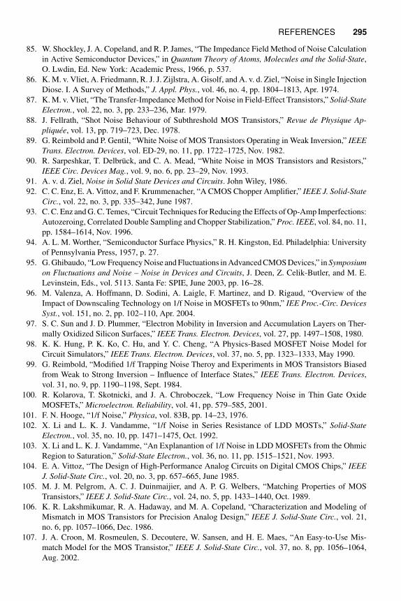
REFERENCES 295
85. W. Shockley, J. A. Copeland, and R. P. James, “The Impedance Field Method of Noise Calculation
in Active Semiconductor Devices,” in Quantum Theory of Atoms, Molecules and the Solid-State,
O. Lwdin, Ed. New York: Academic Press, 1966, p. 537.
86. K. M. v. Vliet, A. Friedmann, R. J. J. Zijlstra, A. Gisolf, and A. v. d. Ziel, “Noise in Single Injection
Diose. I. A Survey of Methods,” J. Appl. Phys., vol. 46, no. 4, pp. 1804–1813, Apr. 1974.
87. K. M. v. Vliet, “The Transfer-Impedance Method for Noise in Field-Effect Transistors,” Solid-State
Electron., vol. 22, no. 3, pp. 233–236, Mar. 1979.
88. J. Fellrath, “Shot Noise Behaviour of Subthreshold MOS Transistors,” Revue de Physique Ap-
pliquee, vol. 13, pp. 719–723, Dec. 1978.
89. G. Reimbold and P. Gentil, “White Noise of MOS Transistors Operating in Weak Inversion,” IEEE
Trans. Electron. Devices, vol. ED-29, no. 11, pp. 1722–1725, Nov. 1982.
90. R. Sarpeshkar, T. Delbruck, and C. A. Mead, “White Noise in MOS Transistors and Resistors,”
IEEE Circ. Devices Mag., vol. 9, no. 6, pp. 23–29, Nov. 1993.
91. A. v. d. Ziel, Noise in Solid State Devices and Circuits. John Wiley, 1986.
92. C. C. Enz, E. A. Vittoz, and F. Krummenacher, “A CMOS Chopper Amplifier,” IEEE J. Solid-State
Circ., vol. 22, no. 3, pp. 335–342, June 1987.
93. C. C. Enz and G. C. Temes, “Circuit Techniques for Reducing the Effects of Op-Amp Imperfections:
Autozeroing, Correlated Double Sampling and Chopper Stabilization,” Proc. IEEE, vol. 84, no. 11,
pp. 1584–1614, Nov. 1996.
94. A. L. M. Worther, “Semiconductor Surface Physics,” R. H. Kingston, Ed. Philadelphia: University
of Pennsylvania Press, 1957, p. 27.
95. G. Ghibaudo, “Low Frequency Noise and Fluctuations in Advanced CMOS Devices,” in Symposium
on Fluctuations and Noise – Noise in Devices and Circuits, J. Deen, Z. Celik-Butler, and M. E.
Levinstein, Eds., vol. 5113. Santa Fe: SPIE, June 2003, pp. 16–28.
96. M. Valenza, A. Hoffmann, D. Sodini, A. Laigle, F. Martinez, and D. Rigaud, “Overview of the
Impact of Downscaling Technology on 1/f Noise in MOSFETs to 90nm,” IEE Proc.-Circ. Devices
Syst., vol. 151, no. 2, pp. 102–110, Apr. 2004.
97. S. C. Sun and J. D. Plummer, “Electron Mobility in Inversion and Accumulation Layers on Ther-
mally Oxidized Silicon Surfaces,” IEEE Trans. Electron. Devices, vol. 27, pp. 1497–1508, 1980.
98. K. K. Hung, P. K. Ko, C. Hu, and Y. C. Cheng, “A Physics-Based MOSFET Noise Model for
Circuit Simulators,” IEEE Trans. Electron. Devices, vol. 37, no. 5, pp. 1323–1333, May 1990.
99. G. Reimbold, “Modified 1/f Trapping Noise Theroy and Experiments in MOS Transistors Biased
from Weak to Strong Inversion – Influence of Interface States,” IEEE Trans. Electron. Devices,
vol. 31, no. 9, pp. 1190–1198, Sept. 1984.
100. R. Kolarova, T. Skotnicki, and J. A. Chroboczek, “Low Frequency Noise in Thin Gate Oxide
MOSFETs,” Microelectron. Reliability, vol. 41, pp. 579–585, 2001.
101. F. N. Hooge, “1/f Noise,” Physica, vol. 83B, pp. 14–23, 1976.
102. X. Li and L. K. J. Vandamme, “1/f Noise in Series Resistance of LDD MOSTs,” Solid-State
Electron., vol. 35, no. 10, pp. 1471–1475, Oct. 1992.
103. X. Li and L. K. J. Vandamme, “An Explanantion of 1/f Noise in LDD MOSFETs from the Ohmic
Region to Saturation,” Solid-State Electron., vol. 36, no. 11, pp. 1515–1521, Nov. 1993.
104. E. A. Vittoz, “The Design of High-Performance Analog Circuits on Digital CMOS Chips,” IEEE
J. Solid-State Circ., vol. 20, no. 3, pp. 657–665, June 1985.
105. M. J. M. Pelgrom, A. C. J. Duinmaijier, and A. P. G. Welbers, “Matching Properties of MOS
Transistors,” IEEE J. Solid-State Circ., vol. 24, no. 5, pp. 1433–1440, Oct. 1989.
106. K. R. Lakshmikumar, R. A. Hadaway, and M. A. Copeland, “Characterization and Modeling of
Mismatch in MOS Transistors for Precision Analog Design,” IEEE J. Solid-State Circ., vol. 21,
no. 6, pp. 1057–1066, Dec. 1986.
107. J. A. Croon, M. Rosmeulen, S. Decoutere, W. Sansen, and H. E. Maes, “An Easy-to-Use Mis-
match Model for the MOS Transistor,” IEEE J. Solid-State Circ., vol. 37, no. 8, pp. 1056–1064,
Aug. 2002.
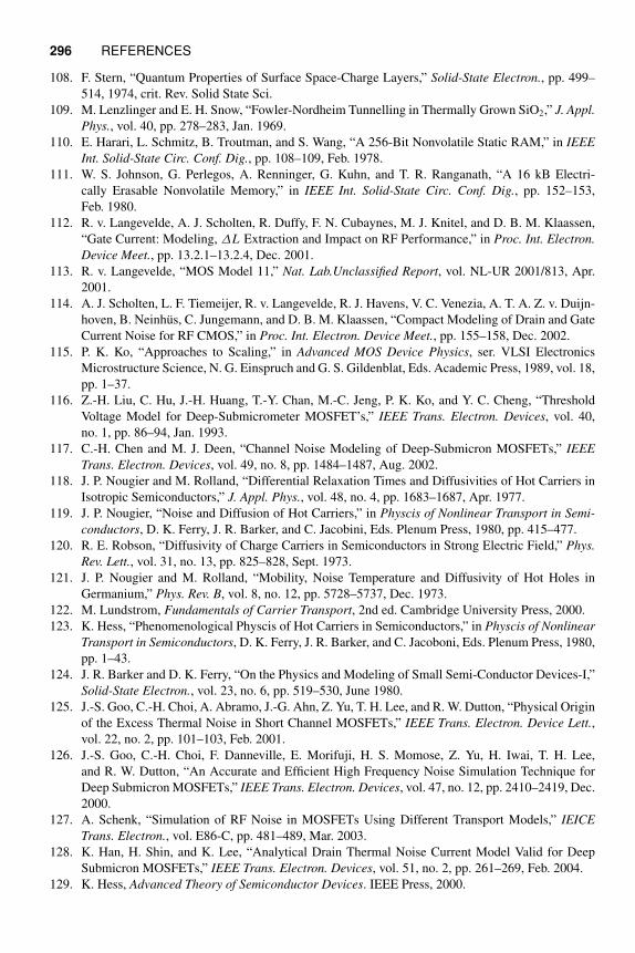
296 REFERENCES
108. F. Stern, “Quantum Properties of Surface Space-Charge Layers,” Solid-State Electron., pp. 499–
514, 1974, crit. Rev. Solid State Sci.
109. M. Lenzlinger and E. H. Snow, “Fowler-Nordheim Tunnelling in Thermally Grown SiO2,” J. Appl.
Phys., vol. 40, pp. 278–283, Jan. 1969.
110. E. Harari, L. Schmitz, B. Troutman, and S. Wang, “A 256-Bit Nonvolatile Static RAM,” in IEEE
Int. Solid-State Circ. Conf. Dig., pp. 108–109, Feb. 1978.
111. W. S. Johnson, G. Perlegos, A. Renninger, G. Kuhn, and T. R. Ranganath, “A 16 kB Electri-
cally Erasable Nonvolatile Memory,” in IEEE Int. Solid-State Circ. Conf. Dig., pp. 152–153,
Feb. 1980.
112. R. v. Langevelde, A. J. Scholten, R. Duffy, F. N. Cubaynes, M. J. Knitel, and D. B. M. Klaassen,
“Gate Current: Modeling, ∆L Extraction and Impact on RF Performance,” in Proc. Int. Electron.
Device Meet., pp. 13.2.1–13.2.4, Dec. 2001.
113. R. v. Langevelde, “MOS Model 11,” Nat. Lab.Unclassified Report, vol. NL-UR 2001/813, Apr.
2001.
114. A. J. Scholten, L. F. Tiemeijer, R. v. Langevelde, R. J. Havens, V. C. Venezia, A. T. A. Z. v. Duijn-
hoven, B. Neinhus, C. Jungemann, and D. B. M. Klaassen, “Compact Modeling of Drain and Gate
Current Noise for RF CMOS,” in Proc. Int. Electron. Device Meet., pp. 155–158, Dec. 2002.
115. P. K. Ko, “Approaches to Scaling,” in Advanced MOS Device Physics, ser. VLSI Electronics
Microstructure Science, N. G. Einspruch and G. S. Gildenblat, Eds. Academic Press, 1989, vol. 18,
pp. 1–37.
116. Z.-H. Liu, C. Hu, J.-H. Huang, T.-Y. Chan, M.-C. Jeng, P. K. Ko, and Y. C. Cheng, “Threshold
Voltage Model for Deep-Submicrometer MOSFET’s,” IEEE Trans. Electron. Devices, vol. 40,
no. 1, pp. 86–94, Jan. 1993.
117. C.-H. Chen and M. J. Deen, “Channel Noise Modeling of Deep-Submicron MOSFETs,” IEEE
Trans. Electron. Devices, vol. 49, no. 8, pp. 1484–1487, Aug. 2002.
118. J. P. Nougier and M. Rolland, “Differential Relaxation Times and Diffusivities of Hot Carriers in
Isotropic Semiconductors,” J. Appl. Phys., vol. 48, no. 4, pp. 1683–1687, Apr. 1977.
119. J. P. Nougier, “Noise and Diffusion of Hot Carriers,” in Physcis of Nonlinear Transport in Semi-
conductors, D. K. Ferry, J. R. Barker, and C. Jacobini, Eds. Plenum Press, 1980, pp. 415–477.
120. R. E. Robson, “Diffusivity of Charge Carriers in Semiconductors in Strong Electric Field,” Phys.
Rev. Lett., vol. 31, no. 13, pp. 825–828, Sept. 1973.
121. J. P. Nougier and M. Rolland, “Mobility, Noise Temperature and Diffusivity of Hot Holes in
Germanium,” Phys. Rev. B, vol. 8, no. 12, pp. 5728–5737, Dec. 1973.
122. M. Lundstrom, Fundamentals of Carrier Transport, 2nd ed. Cambridge University Press, 2000.
123. K. Hess, “Phenomenological Physcis of Hot Carriers in Semiconductors,” in Physcis of Nonlinear
Transport in Semiconductors, D. K. Ferry, J. R. Barker, and C. Jacoboni, Eds. Plenum Press, 1980,
pp. 1–43.
124. J. R. Barker and D. K. Ferry, “On the Physics and Modeling of Small Semi-Conductor Devices-I,”
Solid-State Electron., vol. 23, no. 6, pp. 519–530, June 1980.
125. J.-S. Goo, C.-H. Choi, A. Abramo, J.-G. Ahn, Z. Yu, T. H. Lee, and R. W. Dutton, “Physical Origin
of the Excess Thermal Noise in Short Channel MOSFETs,” IEEE Trans. Electron. Device Lett.,
vol. 22, no. 2, pp. 101–103, Feb. 2001.
126. J.-S. Goo, C.-H. Choi, F. Danneville, E. Morifuji, H. S. Momose, Z. Yu, H. Iwai, T. H. Lee,
and R. W. Dutton, “An Accurate and Efficient High Frequency Noise Simulation Technique for
Deep Submicron MOSFETs,” IEEE Trans. Electron. Devices, vol. 47, no. 12, pp. 2410–2419, Dec.
2000.
127. A. Schenk, “Simulation of RF Noise in MOSFETs Using Different Transport Models,” IEICE
Trans. Electron., vol. E86-C, pp. 481–489, Mar. 2003.
128. K. Han, H. Shin, and K. Lee, “Analytical Drain Thermal Noise Current Model Valid for Deep
Submicron MOSFETs,” IEEE Trans. Electron. Devices, vol. 51, no. 2, pp. 261–269, Feb. 2004.
129. K. Hess, Advanced Theory of Semiconductor Devices. IEEE Press, 2000.
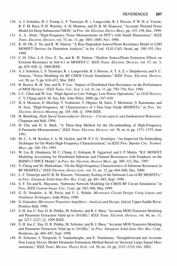
REFERENCES 297
130. A. J. Scholten, H. J. Tromp, L. F. Tiemeijer, R. v. Langevelde, R. J. Havens, P. W. H. d. Vreede,
R. F. M. Roes, P. H. Woerlee, A. H. Montree, and D. B. M. Klaassen, “Accurate Thermal Noise
Model for Deep-Submicron CMOS,” in Proc. Int. Electron. Device Meet., pp. 155–158, Dec. 1999.
131. A. A. Abidi, “High-Frequency Noise Measurements on FET’s with Small Dimensions,” IEEE
Trans. Electron. Devices, vol. 33, no. 11, pp. 1801–1805, Nov. 1986.
132. K.-H. Oh, Z. Yu, and R. W. Dutton, “A Bias Dependent Source/Drain Resistance Model in LDD
MOSFET Devices for Distortion Analysis,” in Int. Conf. VLSI CAD, Seoul, pp. 190–193, Oct.
1999.
133. C.-H. Choi, J.-S. Goo, Z. Yu, and R. W. Dutton, “Shallow Source/Drain Extension Effects on
External Resistance in Sub-0.1 m MOSFET’s,” IEEE Trans. Electron. Devices, vol. 47, no. 3,
pp. 655–658, c© 2000 IEEE.
134. A. J. Scholten, L. F. Tiemeijer, R. v. Langevelde, R. J. Havens, A. T. A. Z. v. Duijnhoven, and V. C.
Venezia, “Noise Modeling for RF CMOS Circuit Simulation,” IEEE Trans. Electron. Devices,
vol. 50, no. 5, pp. 618–632, Mar. 2003.
135. B. Razavi, R.-H. Yan, and K. F. Lee, “Impact of Distributed Gate Resistance on the Performance
of MOS Devices,” IEEE Trans. Circ. Syst. I, vol. 41, no. 11, pp. 750–754, Nov. 1994.
136. I. C. Chen and W. Liu, “High-Speed or Low-Voltage, Low-Power Operations,” in ULSI Devices,
C. Y. Chang and S. M. Sze, Eds. John Wiley, 2000, pp. 547–630.
137. H. S. Momose, E. Morifuji, T. Yoshitomi, T. Ohguro, M. Saito, T. Morimoto, Y. Katsumata, and
H. Iwai, “High-Frequency AC Characteristics of 1.5nm Gate Oxide MOSFETs,” in Proc. Int.
Electron. Devices Meeting, pp. 105–108, c© 1996 IEEE.
138. H. Beneking, High Speed Semiconductor Devices – Circuit aspects and fundamental Behaviour.
Chapman and Hall, 1994.
139. H. Cho and D. E. Burk, “A Three-Step Method for the De-embedding of High-Frequency
S-Parameter Measurements,” IEEE Trans. Electron. Devices, vol. 38, no. 6, pp. 1371–1375, June
1991.
140. M. C. A. M. Koolen, J. A. M. Geelen, and M. P. J. G. Versleijen, “An Improved De-Embedding
Technique for On-Wafer High-Frequency Characterization,” in IEEE Proc. Bipolar Circ. Technol.
Meet., pp. 188–191, 1991.
141. W. Liu, R. Gharpurey, M. C. Chang, U. Erdogan, R. Aggarwal, and J. P. Mattia, “R.F. MOSFET
Modeling Accounting for Distributed Substrate and Channel Resistances with Emphasis on the
BSIM3v3 SPICE Model,” in Proc. Int. Electron. Devices Meet., pp. 309–312, Dec. 1997.
142. Y. Cheng and M. Matloubian, “On the High-Frequency Characteristics of Substrate Resistance in
RF MOSFETs,” IEEE Electron. Device Lett., vol. 21, no. 12, pp. 604–606, Dec. 2000.
143. L. F. Tiemeijer and D. B. M. Klassen, “Geometry Scaling of the Substrate Loss of RF MOSFETs,”
in Proc. European Solid-State Dev. Res. Conf., pp. 481–483, Sept. 1998.
144. S. F. Tin and K. Mayaram, “Substrate Network Modeling for CMOS RF Circuit Simulation,” in
Proc. IEEE Custom Integr. Circ. Conf., pp. 583–586, May 1999.
145. G. D. Vendelin, A. M. Pavio, and U. L. Rohde, Microwave Circuit Design Using Linear and
Nonlinear Techniques. John Wiley, 1990.
146. G. Gonzalez, Microwave Transistor Amplifiers – Analysis and Design, 2nd ed. Upper Saddle River:
Prentice-Hall, 1996.
147. S. H. Jen, C. Enz, D. R. Pehlke, M. Schroter, and B. J. Sheu, “Accurate MOS Transistor Modeling
and Parameter Extraction Valid up to 10-GHz,” IEEE Trans. Electron. Devices, vol. 46, no. 11,
pp. 2217–2227, c© 1999 IEEE.
148. S. H. Jen, C. Enz, D. R. Pehlke, M. Schroter, and B. J. Sheu, “Accurate MOS Transistor Modeling
and Parameter Extraction Valid up to 10-GHz,” in Proc. European Solid-State Dev. Res. Conf.,
Bordeaux, pp. 484–487, Sept. 1998.
149. D. Schreurs, J. Verspecht, S. Vandenberghe, and E. Vandamme, “Straightforward and Accurate
Non Linear Device Model Parameter Estimation Method Based on Vectorial Large-Signal Mea-
surements,” IEEE Trans. Microw. Theory Tech., vol. 50, no. 10, pp. 2315–2319, Oct. 2002.
298 REFERENCES
150. H. Johnson, “Noise in Field-Effect Transistors,” in Field-Effect Transistors, J. T. Wallmark and
H. Johnson, Eds. Englewood Cliffs, NJ: Prentice-Hall, 1966, pp. 160–186.
151. T. H. Lee, The Design of CMOS Radio-Frequency Integrated Circuits, 2nd ed. Cambridge:
Cambridge University Press, 1998.
152. E. Morifuji, H. S. Momose, T. Ohguro, T. Yoshitomi, H. Kimijima, F. Matsuoka, M. Kinugawa,
Y. Katsumata, and H. Iwai, “Future Perspective and Scaling Down Roadmap for RF CMOS,” in
Dig. Tech. Pap. Symp. VLSI Technol., pp. 163–164, June 1999.
153. A.-S. Porret and C. C. Enz, “Non-Quasi-Static (NQS) Thermal Noise Modelling of the MOS
Transistor,” IEE Proc.-Circ. Devices Syst., vol. 151, no. 2, pp. 155–166, Apr. 2004.
154. L.-J. Pu and Y. Tsividis, “Small-Signal Parameters and Thermal Noise of the Four-Terminal MOS-
FET in Non-Quasistatic Operation,” Solid-State Electron., vol. 33, no. 5, pp. 513–521, May 1990.
155. C. H. Chen and M. J. Deen, “High Frequency Noise of MOSFETs – Part I: Modeling,” Solid-State
Electron., vol. 42, no. 11, pp. 2069–2081, Nov. 1998.
156. A. S. Roy, C. C. Enz and J.-M. Sallese, “Noise modeling methodologies in the presence of mobility
degradation and their equivalence,” IEEE Trans. on Electron Devices, vol. 53, no. 2, pp. 348–355,
Feb. 2006.
Index
Accumulation, 19, 216, 221
Active region, 9
Admittance
gate-to-bulk, 68, 274
gate-to-source, 68, 270, 274
gate-to-drain, 68, 270, 274
bulk-to-drain, 68, 270
bulk-to-source, 68, 270
substrate, 255
correlation, 263, 261, 265
Band gap, 112
extrapolated, 113
widening, 156, 133, 157, 158, 160, 161
Bode theorem, 106–107, 92, 274n
Boltzmann constant, 10, 87
Capacitance
gate oxide, 17, 214
silicon, 18, 19, 224
gate, 13, 18, 19, 30, 73, 233
depletion, 19, 30
intrinsic, 70, 72, 73, 75, 233
overlap, 214, 220, 221, 222, 223, 232, 233
junction, 54, 214, 224–226, 232, 244, 249, 288
fringing-field, 220, 221, 222, 233,
bottom-wall, 220, 226
side-wall, 226
Capacitor
overlap, 10, 66, 77
Carrier
fluctuations, 96, 100
heating, 167, 205–209, 211, 285
Cascode configuration, 226
Channel
buried, 143, 144, 145
homogeneous, 47–49
length, 46, 53, 54, 60, 164–167, 176, 186–188,
198, 208, 232, 285
length modulation, 33, 48, 50, 52–54, 167,
186–188, 208
narrow, 50
residual current, 45
voltage, 34, 38, 43, 49, 52, 78, 83, 116
width, 34, 46, 60, 164, 218
gradual, 13, 14, 16, 167, 187, 189
conductance, 86, 89, 90, 199, 201
region, 14, 51, 81, 198, 218, 219, 222, 223, 231
Channel length modulation, 48, 50, 52–54, 167,
186–188, 208
Charge
elementary, 10, 189, 227
fixed, 10, 11, 15–17, 150, 151, 155, 187
inversion, 4, 10, 11, 20, 21, 24, 30, 65, 87, 96,
143, 146, 171–176, 206, 211
total, 11, 13, 17, 21, 27, 144
concentration, 13, 14, 33, 187
depletion, 11, 12, 15, 17, 21, 23, 26, 30, 47, 49,
97, 134, 138, 157, 224
specific, 13, 24, 32, 117, 133, 154, 161
Charge density, 11
depletion, 11, 12, 15, 17, 19, 21, 26, 30, 47, 97,
134, 138, 157, 224
in silicon, 23, 27, 189
inversion, 20, 21, 25, 30, 65, 87, 96, 143, 148,
172–176, 192, 211
specific, 13, 24, 32, 117, 133, 154, 159, 161
fixed, 11, 17, 150, 151, 155, 187
Charge-Based MOS Transistor Modeling: The EKV Model for Low-Power and RF IC Design C. Enz and E. VittozC© 2006 John Wiley & Sons, Ltd.
300 INDEX
Charge sheet approximation, 13, 20, 21, 23, 33,
158
Charge-potential linearization, 23–32
Common-source amplifier, 233, 261, 282,
286–288
Concentration
hole, 14
intrinsic carrier, 14, 112, 113
electron, 14, 20, 158, 187
doping, 14, 47, 51, 60, 114, 138, 142, 147, 149,
159, 160, 223
Concentric transistor, 54
Conductance
drain-to-source, 60, 89
specific, 57, 119, 154, 219
Critical field, 91, 167–169, 171, 180
Current
drain, 10, 33, 168, 171–174, 179, 182, 184,
191, 194, 203, 217, 225, 274, 282
forward, 35, 48, 56, 63, 133, 163, 164
gate leakage, 106, 133, 161–166, 223
reverse, 35, 37, 39, 42, 56, 58, 62, 133,
135–137, 224
specific, 37, 40, 52, 65, 118, 154, 161
drift, 10, 33, 34
diffusion, 10, 33, 34, 49, 54, 89, 166, 171, 172,
213, 215, 223, 246
tunneling, 220, 227
generation, 223, 224
gain, 83, 232, 233, 234, 237
Debye length, 15
Depletion
thickness, 19, 189
capacitance, 17, 19, 30
Dielectric constant of silicon, 14
Differential pair, 122, 129
Diffusivity, 202
Doping
concentration, 7, 9, 13, 14, 16, 47, 51, 60, 114,
118, 138, 142–147, 159, 223
ratio, 141, 143, 145–148
Drain, 3, 4, 7, 9, 10
induced barrier lowering (DIBL), 167,
189–197
voltage, 3, 7, 10, 207, 208, 210
Drain current, 10, 11, 25, 33, 40–46, 55, 60,
65, 83, 85, 88, 100–104, 127, 133, 154,
171
alternative models of, 36, 43, 45, 194
general expression, 37, 42, 46, 55, 59
in strong inversion, 13, 18, 19, 31, 41, 52, 58,
63, 75, 95, 102
in weak inversion, 17, 26, 36, 43, 52, 64, 74,
89, 105, 118
Ebers-Moll model, 3, 46
Einstein relation, 202
Electric field
longitudinal, 33, 205
effective, 134, 156, 171, 186
vertical, 15, 134, 135
Energy band gap of silicon, 112
Equilibirum, 10
Extrinsic
part, 9, 131, 213, 222, 231, 257
noise sources, 227, 228
Fast surface state, 11
Figure of merit, 64, 90, 105, 232, 236–238
Flat-band condition, 17, 114, 150, 221
Flicker noise, 81, 86, 96–106, 226, 227
corner frequency, 96
Fluctuations
mobility, 96, 101, 104–106
carrier, 96
resistance, 103
of width, 126
of length, 126
Gate
capacitance, 13, 18–20
doping, 114, 115
leakage current, 133, 161, 163, 223
modulation factor, 149
oxide capacitance, 17
overhead voltage, 41
Gate-drain noise correlation factor, 278
Gauss’ law, 16, 17, 134, 186, 189
Geometrical effects, 53, 54
Grading coefficient, 225
Gradual channel approximation, 14, 16, 17, 167,
187, 189
Harmonic distortion, 216
High injection, 223
Hooge
model, 101, 102
parameter, 101, 105
Impedance field method, 83
Induced gate noise, 83, 262, 273, 281, 282
INDEX 301
Induced substrate noise, 271
Intrinsic
part, 9, 10, 66, 77, 81, 213
capacitances, 73–74, 249, 275
channel time constant, 65, 275
nodes, 216
Inversion charge density
in weak inversion, 26
in strong inversion, 26
at the drain, 38, 78
at the source, 38
Inversion coefficient (or factor), 40–44, 53
Langevin, 83
method, 82, 83
noise source, 83
Lateral bipolar transistor, 12
Linear mode, 36, 40, 42, 52, 59
Low-noise amplifiers, 218, 257
Matching, 120–129
Maximum available gain, 236
Maximum frequency of oscillation, 236
Microscopic noise source, 84
Minimum noise figure, 231, 238, 239, 261, 266,
287
Mismatch, 111, 120, 122, 123, 129
of drain current, 122, 127
of gate voltage, 122, 124
systematic, 124
random, 125–128
Mobility, 33
effective, 168–171
fluctuations, 101, 106
nonuniform, 138
reduction due to the vertical field, 133, 205, 209
temperature variation, 113–115
low field, 133
field dependent, 133, 172, 203
differential, 168, 200, 202
cord, 168, 203–206
Mode of operation
linear, 36, 42
triode, 36
nonsaturation, 36
weak inversion, 36
strong inversion, 36
subthreshold, 37, 43
blocked, 37
bipolar, 37
Moderate inversion, 37, 41, 64, 102, 105
Noise
factor, 238, 265
figure, 238
matching, 238, 267, 285
parameters, 91, 261, 285, 286, 290
Nonquasi-static
small-signal circuit, 67, 82, 93, 94, 229, 249
operation, 65, 249, 257
large-signal operation, 77–79, 249
Normalization
frequency, 68, 70, 72
bias, 70, 72
Normalized
drain current, 37, 88, 154, 194
inversion charge density, 24, 38, 65
inversion charge density at the drain, 38, 57,
173
inversion charge density at the source, 38, 57,
173
voltages, 24, 41
pinch-off voltage, 24, 43, 67, 73, 135, 156
forward current, 37, 63
reverse current, 37, 135–137
intrinsic capacitances, 73, 74
transconductances, 57, 181, 182
transcapacitances, 75, 76
Nyquist theorem, 106–107, 274
Operating point, 56, 68, 81, 90, 168
Optimum source admittance, 261, 267
Overlap region, 216, 221, 223
Oxide
charge in, 11
field, 11
thickness, 9, 10
gate, 9
Physical parameters, 111, 112, 115, 120
spatial fluctuations of, 120
statistical fluctuations, 125
Pinch-off
potential, 22, 25, 145, 147, 159
voltage, 25, 209–211
Poisson
distribution, 128
equation, 14, 51
Potential
barrier, 51, 89, 190, 194
electrostatic, 11, 49, 50
surface, 11, 14, 17, 52, 97
extraction, 11, 114, 115
302 INDEX
Potential (Cont.)
Fermi, 14, 34, 113, 114
pinch-off, 22, 25, 145, 147, 159
Power spectral density (PSD), 81
of drain current, 87
Pseudo-resistor, 33, 49, 165
Quad configuations, 125
Quasi-Fermi potential, 10, 14, 34
Quasi-static
frequency, 65, 66, 275
time constant, 65, 75, 92, 275
small-signal circuit, 76, 92, 249
Random fluctuations
of carrier velocity, 81, 83
of carrier density, 81
Resistance
access, 213, 215, 216–219, 247
gate, 14, 213, 217, 247, 252
source, 213, 215, 287
drain, 102, 213, 215, 217, 226
substrate, 214, 226, 243–246
salicide, 215
via, 215, 218
contact, 215
Sample-and-hold, 92
Saturation
forward, 36, 40, 42, 54, 60, 70
reverse, 36, 53, 60, 70, 71
Saturation mode, 36, 40
forward, 36, 40, 42, 54, 60, 70
reverse, 36, 53, 60, 70, 71
Saturation voltage, 36, 42, 66, 173
Scattering
mechanisms, 96, 115, 134
due to acoustic phonon, 115
due to ionized impurities, 115
Short-channel effects, 48, 131, 167–212
Silicon dioxide, 9, 161
Slope factor, 21, 23, 25, 162
charge, 153, 162
evaluation of, 29–31
voltage, 152
Source-drain extension, 215
Space charge regions, 51
Spacer, 216, 220
Spatial correlation, 109, 125
Specific conductance, 57, 119, 154, 219
Step profile, 141–144, 148, 225
Strong inversion, 17, 232–234, 239, 252
charge approximation, 20, 21, 27, 155
current approximation, 41, 194
Substrate modulation factor, 21, 116, 140, 159
Substrate network, 214, 242–247, 249
Subthreshold mode, 37
Surface
electric field, 11, 47, 49, 144
potential, 11, 17, 21, 23, 38, 52, 189
Symmetry, 46, 68
source and drain, 9, 56
Temperature
absolute, 10, 87, 112
effects on transistor, 111–120
noise, 202
carrier, 202
lattice, 203, 205
Temperature coefficient of
Fermi voltage, 114
extraction voltage, 115
threshold voltage, 117
inversion charge, 117, 120
specific current, 118
transconductances, 119
Thermal noise
conductance at the drain, 87, 203
excess factor, 89, 90–91, 93–95, 206–212
parameter, 81, 89, 90–92, 206–212
voltage variance, 95
short-channel, 197–212
Threshold
function, 13, 21, 22, 27, 29, 116, 138, 140, 142,
150
voltage (at equilibrium), 28
Threshold function, 21
Transadmittance
drain, 66–68
source, 66–68
gate, 66–68
Transcapacitances
gate, 75
drain, 74
source, 74
Transconductance
bulk, 288
drain, 56–60, 62, 136, 154
gate, 56, 197, 234, 288
source, 56, 60, 154, 183, 201, 234
effective, 216
intrinsic, 216
INDEX 303
Transconductance-to-current ratio, 62, 183
Transducer gain, 237
Transfer parameter, 34, 40, 118, 121
Transistor
bipolar, 12, 37, 45, 229
extrinsic part, 9, 131, 213, 214, 227, 231
intrinsic part, 9, 61, 66, 213, 214
schematic cross section, 10
symbols, 12
Transit frequency, 55, 66, 232, 233, 234, 235,
239, 268, 287
peak, 234
Transit time, 239, 240
total, 239
of intrinsic part, 239
of extrinsic part, 239
Trapping, 96, 98, 100
Tunneling, 98
Unilateral power gain, 236, 237
Unity gain transit frequency, 233
Velocity
Saturation, 86, 167, 168, 171, 177, 232, 235
saturation region, 186, 187
drift, 167, 168, 173
Velocity-field models, 169–171
Voltage
channel length modulation, 60
drain, 10, 33, 35, 36, 38, 42, 56, 60, 170, 171
gain, 61, 64, 167, 197, 198
gate, 10, 17, 18, 23, 25, 27, 32, 35, 40, 50, 143,
150, 153
pinch-off, 3, 25, 32, 35, 36, 43, 135, 180, 211
intrinsic, 216
saturation, 37, 44
source, 10
thermodynamic, 10, 83
channel, 9, 14, 19, 23, 25, 26, 77, 83, 116
flat-band, 17, 49, 50, 52, 114, 221
band gap, 112
extrapolated band gap, 113
avalanche breakdown, 224
Weak inversion, 17, 18, 20, 26, 30, 36, 39
current approximation, 43–45
Well
perimeter, 226
area, 226
Y-parameters, 234, 237, 243, 249, 251, 252, 253,
255, 261, 263, 265, 273