Embed Size (px)
Citation preview
jm
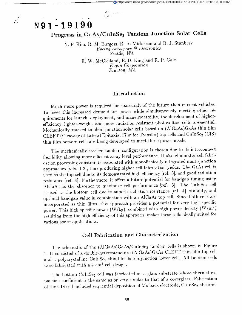
N91-19190
Progress in GaAs/CuInSe2 Tandem Junction Solar Cells
N. P. Kim, R. M. Burgess, R. A. Mickelsen and B. J. StanberyBoeing Aerospace _d Electronics
Seattle, WA
R. W. McClelland, B. D. King and R. P. GaleKopin Corporation
Taunton, MA
Introduction
Much more power is required for spacecraft of the future than current vehicles.
To meet this increased demand for power while simultaneously meeting other re-
quirements for launch, deployment, and maneuverability, the development of higher-
efficiency, lighter-weight, and more radiation resistant photovoltaie cells is essential.
Mechanically stacked tandem junction solar cells based on (A1GaAs)GaAs thin film
CLEFT (Cleavage of Lateral Epitaxial Film for Transfer) top cells and CulnSe 2 (CIS)
thin film bottom cells are being developed to meet these power needs.
The mechanically stacked tandem configuration is chosen due to its interconnect
flexibility allowing more efficient array level performance. It also eliminates cell fabri-
cation processing constraints associated with monolithically integrated multi-junction
approaches [refs. 1-2], thus producing higher cell fabrication yields. The GaAs cell is
used as the top cell due to its demonstrated high efficiency [ref. 3], and good radiation
resistance [ref. 4]. Furthermore, it offers a future potential for bandgap tuning using
A1GaAs as the absorber to maximize cell performance [ref. 5]. The CulnSe2 cell
is used as the bottom cell due to superb radiation resistance [ref. 4], stability, and
optimal bandgap value in combination with an A1GaAs top cell. Since both cells are
incorporated as thin films, this approach provides a potential for very high specific
power. This high specific power (W/kg), combined with high power density (W/m 2)
resulting from the high efficiency of this approach, makes these cells ideally suited for
various space applications.
Cell Fabrication and Characterization
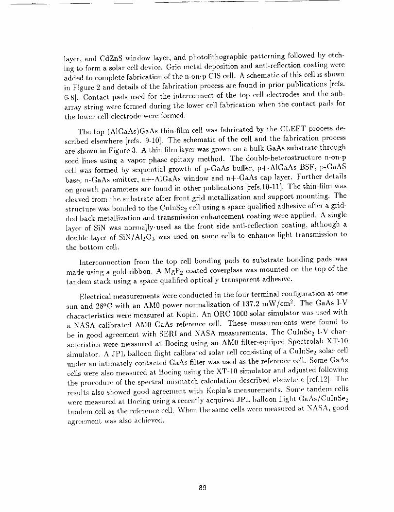
The schematic of the (A1GaAs)GaAs/CuInSe2 tandem cells is shown in Figure
1. It consisted of a donble-heterostructure (A1GaAs)GaAs CLEFT thin-film top cell
and a polycrystalline CuInSe2 thin-fihn heterojunction lower cell. All tandem cells
were fabricated with a 4 cm 2 cell design.
The bottom CulnSe2 cell was fabricated on a glass substrate whose thermal ex-
pansion coefficient is the same as or very similar to that of a coverglass. Fabrication
of tile CIS cell included sequential deposition of Mo back electrode, CuInSe 2 absorber
88
https://ntrs.nasa.gov/search.jsp?R=19910009877 2020-08-07T06:01:38+00:00Z
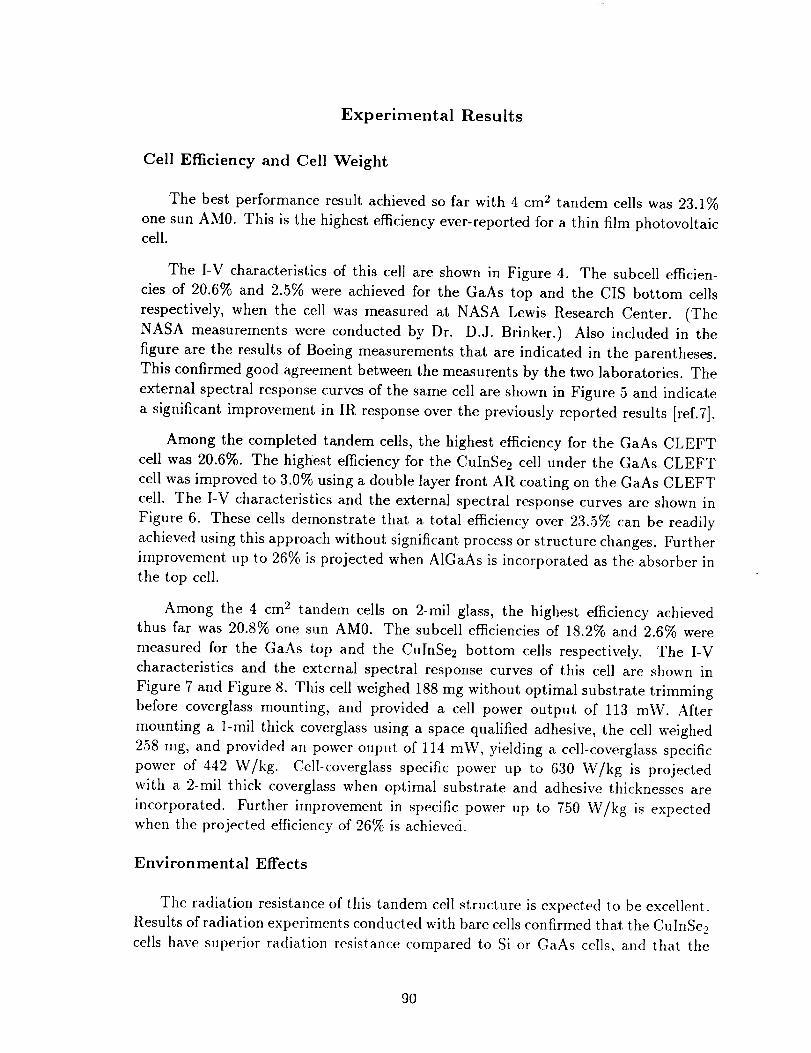
layer, and CdZnSwindow layer, and photolithographic patterning followed by etch-ing to form a solar cell device. Grid metal depositionand anti-reflection coating wereaddedto complete fabrication of the n-on-p CIS cell. A schematic of this cell is shown
in Figure 2 and details of the fabrication process are found in prior publications [refs.
6-8]. Contact pads used for the interconnect of the top cell electrodes and the sub-
array string were formed during the lower cell fabrication when the contact pads for
the lower cell electrode were formed.
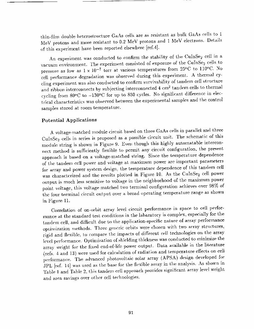
The top (A1GaAs)GaAs thin-film cell was fabricated by the CLEFT process de-
scribed elsewhere [refs. 9-10]. The schematic of the cell and the fabrication process
are shown in Figure 3. A thin film layer was grown on a bulk GaAs substrate through
seed lines using a vapor phase epitaxy method. The double-heterostructure n-on-p
cell was formed by sequential growth of p-GaAs buffer, p+-A1GaAs BSF, p-GaAS
base, n-GaAs emitter, n+-A1GaAs window and n+-GaAs cap layer. Further details
on growth parameters are found in other publications [refs.10-11]. The thin-film was
cleaved from the substrate after front grid metallization and support mounting. The
structure was bonded to the CulnSe_ cell using a space qualified adhesive after a grid-
ded back metallization and transmission enhancement coating were applied. A single
layer of SiN was norma!ly, used as the front side anti-reflection coating, although a
double layer of SiN/A1203 was used on some cells to enhance light transmission to
the bottom cell.
Interconnection from the top cell bonding pads to substrate bonding pads was
made using a gold ribbon. A MgF2 coated coverglass was mounted on tile top of the
tandem stack using a space qualified optically transparent adhesive.
Electrical measurements were conducted in the four terminal configuration at one
sun and 28°C with an AM0 power normalization of 137.2 mW/cm 2. The GaAs I-V
characteristics were measured at Kopin. An ORC 1000 solar simulator was used with
a NASA calibrated AM0 GaAs reference cell. These measurements were found to
be in good agreement with SERI and NASA measurements. The CulnSe2 I-V char-
acteristics were measured at Boeing using an AM0 filter-equiped Spectrolab XT-10
simulator. A JPL balloon flight calibrated solar cell consisting of a CulnSe2 solar cell
under an intimately contacted GaAs filter was used as the reference cell. Some GaAs
cells were also measured at Boeing using the XT-10 simulator and adjusted following
the procedure of the spectral mismatch calculation described elsewhere [ref.12]. The
results also showed good agreement with Kopin's measurements. Some tandem cells
were measured at Boeing using a recently acquired JPL balloon flight GaAs/CuInSe?,
tandem cell as the reference cell. When tile same cells were measured at NASA, good
agreement was also achieved.
89
Experimental Results
Cell Efficiency and Cell Weight
The best performance result achieved so far with 4 cm 2 tandem cells was 23.1%
one sun AM0. This is the highest efficiency ever-reported for a thin film photovoltaiccell.
The I-V characteristics of this cell are shown in Figure 4. The subcell efficien-
cies of 20.6% and 2.5% were achieved for the GaAs top and the CIS bottom cells
respectively, when the cell was measured at NASA Lewis Research Center. (The
NASA measurements were conducted by Dr. D.J. Brinker.) Also included in the
figure are the results of Boeing measurements that are indicated in the parentheses.
This confirmed good agreement between the measurents by the two laboratories. The
external spectral response curves of the same cell are shown in Figure 5 and indicate
a significant improvement in IR response over the previously reported results [ref.7].
Among the completed tandem cells, the highest efficiency for the GaAs CLEFT
cell was 20.6%. The highest efficiency for the CuInSe2 cell under the GaAs CLEFT
cell was improved to 3.0% using a double layer front AR coating on the GaAs CLEFT
cell. The I-V characteristics and the external spectral response curves are shown in
Figure 6. These cells demonstrate that a total efficiency over 23.5% can be readily
achieved using this approach without significant process or structure changes. Further
improvement up to 26% is projected when A1GaAs is incorporated as the absorber in
the top cell.
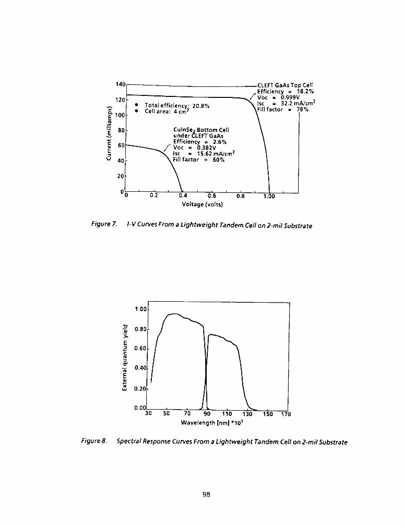
Among the 4 cm 2 tandem cells on 2-mil glass, the highest efficiency achieved
thus far was 20.8% one sun AM0. The subcell efficiencies of 18.2% and 2.6% were
measured for the GaAs top and the CuInSe2 bottom cells respectively. The I-V
characteristics and the external spectral response curves of this cell are shown in
Figure 7 and Figure 8. This cell weighed 188 mg without optimal substrate trimming
before coverglass mounting, and provided a cell power output of 113 mW. After
mounting a 1-mil thick covcrglass using a space qualified adhesive, the cell weighed
258 rag, and provided an power ouput of 114 mW, yielding a cell-coverglass specific
power of 442 W/kg. Cell-coverglass specific power up to 630 W/kg is projected
with a 2-mil thick coverglass when optimal substrate and adhesive thicknesses are
incorporated. Further improvement in specific power up to 750 W/kg is expectedwhen the projected efficiency of 26% is achieved.
Environmental Effects
The radiation resistance of this tandem cell structure is expected to be excellent.
Results of radiation experiments conducted with bare cells confirmed that the CuInSe2
cells have superior radiation resistance compared to Si or C, aAs cells, and that the
9O
thin-film double-heterostructureGaAs cellsare as resistant as bulk GaAs cells to 1MeV protons and more resistant to 0.2 MeV protons and 1 MeV electrons. Detailsof this experimenthavebeenreported elsewhere[ref.4].
An experiment wasconducted to confirm the stability of the CuInSe_cell in avacuumenvironment. The experiment consistedof exposureof the CuInSe2cells topressureas low as 1 x 10 .7 torr at various temperatures from 25°C to 110°C. No
cell performance degradation was observed during this experiment. A thermal cy-
cling experiment was also conducted to confirm survivability of tandem cell structure
and ribbon interconnects by subjecting interconnected 4 cm 2 tandem cells to thermal
cycling from 80°C to -130°C for up to 850 cycles. No significant difference in elec-
trical characteristics was observed between the experimental samples and the control
samples stored at room temperature.
Potential Applications
A voltage-matched module circuit based on three GaAs cells in parallel and three
CulnSe2 cells in series is proposed as a possible circuit unit. The schematic of this
module string is shown in Figure 9. Even though this highly automatable intercon-
nect method is sufficiently flexible to permit any circuit configuration, the present
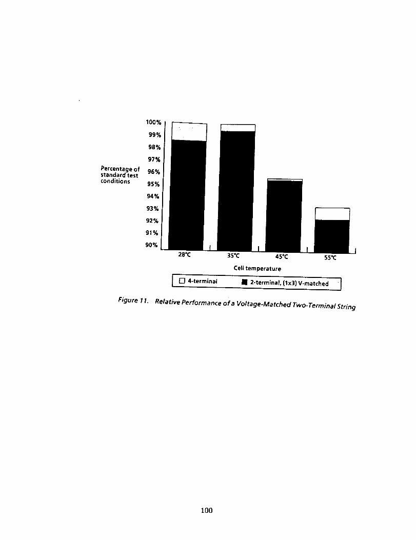
approach is based on a voltage-matched string. Since the temperature dependence
of the tandem cell power and voltage at maximum power are important parameters
for array and power system design, the temperature dependence of this tandem cell
was characterized and the results plotted in Figure 10. As the CuInSe2 cell power
output is much less sensitive to voltage in the neighborhood of the maximum power
point voltage, this voltage-matched two terminal configuration achieves over 98% of
the four terminal circuit output over a broad operating temperature range as shown
in Figure 11.
Correlation of on-orbit array level circuit performance in space to cell perfor-
mance at the standard test conditions in the labaratory is complex, especially for the
tandem cell, and difficult due to the application-specific nature of array performance
optimization methods. Three generic orbits were chosen with two array structures,
rigid and flexible, to compare the impacts of different cell technologies on the array
level performance. Optimization of shielding thickness was conducted to minimize the
array weight for the fixed end-of-life power output. Data available in the literature
(refs. 4 and 13) were used for calculation of radiation and temperature effects on cell
performance. The advanced photovoltaic solar array (APSA) design developed for
JPL [ref. 14] was used as the base for the flexible array in the analysis. As shown in
Table 1 and Table 2, this tandem cell approach provides significant array level weight
and area savings over other cell technologies.
91
Program Status
We have recently increased our tandem cell throughput and fabricated quantities
of cells that produce tens of watts of power in total. A significant increase in cell
throughput and a 2 cm x 4 cm cell design with high active area utilization, and further
performance improvement using A1GaAs instead of GaAs as absorber are currently
being investigated to make GaAs(A1GaAs)/CulnSe 2 tandem cells more viable for
near-term space power applications.
Conclusions
The efficiency of GaAs/CuInSe2 thin-film tandem cells improved to 23.1%, one
sun, AM0. This is the highest efficiency ever-reported for a thin-film photovoltaic
cell. Further improvement up to 26% is projected when an A1GaAs absorber layer is
incorporated in the top cell.
Lightweight GaAs/CuInSe2 tandem cells (2-mil thick) were demonstrated with
efficiencies as high as 20.8%. The cell with a 1-mil thick coverglass weighed 258 mg
even without optimal substrate trimming. This provides a cell-coverglass specific
power of 442 W/kg, and offers a potential for specific powers up to 750 W/kg with
an A1GaAs top cell.
Environmental tests including radiation test, vacuum experiment and thermal cy-
cling test were conducted and provided favorable results. On-array level performance
was analyzed for three generic orbit levels to compare the impact of different cell tech-
nologies, and results indicated that a significant array weight and area savings can
be achieved with these tandem cells. A voltage-matched module circuit is proposed
and its projected performance is discussed. The current status of the program and
the near term plan is also summarized.
References
1. ] H. F. MacMillan, H. C. Hamaker, G. F. Virshup and J. G. Werthen, Con-
ference Record 20th IEEE Photovoltaic Specialist Conference, 48, 1988.
2. ] S. P. Tobin, S. M. Vernon, C. Bajgar, V. E. Haven, L. M. Geoffroy, M. M.
Sanfacon, D. R. Lillington, R. E. Hart, K. A. Emery and R. J. Matson, Conference
Record 20th IEEE Photovoltaic Specialist Conference, 405, 1988.
3. ] N. Ogasawara, S. Ochi, N. Hayafuji, M. Kado, K. Mitsui, K. Yamanaka, and
T. Murotani, Technical Digest of the International PVSEC-3, 477, Tokyo, Japan,1987.
92
[ 4. ] R. M. Burgess, W. S. Chen, W. E. Devaney, D. It. Doyle, N. P. Kim, and
B. J. Stanbery, Conference Record 20th IEEE Photovoltaic Specialist Conference,
909, 1988.
[ 5. ] J. C. C. Fan and B. J. Palm, Solar Cells 12,401, 1984.
[ 6. ] B. J. Stanbery, 3. E. Avery, R. M. Burgess, W. S. Chen, W. E. Devaney,
D. H. Doyle, R. A. Mickelsen, R. W. McClelland, B. D. King, R. P. Gale and
J. C. C. Fan, Conference Record 19th IEEE Photovoltaic Specialist Conference,
280,1987.
[ 7. ] N. P. Kim, R. M. Burgess, B. 3. Stanbery, R. A. Mickelsen, J. E. Avery, R.
W. McClelland, B. D. King, M. J. Boden and R. P. Gale, Conference Record 20th
IEEE Photovoltaic Specialist Conference, 457, 1988.
[ 8. ] R. A. Mickelsen, and W. S. Chen, Conference Record 16th IEEE PhotovoItaie
Specialist Conference, 781, 1982.
[ 9. ] R. W.McClelland, C. O. Bozler and 3. C. C. Fan, Appl. Phys. Lett. 37',
560, 1980.
[ 10. ] R. P. Gale, R. W. McClelland, B. D. King and J. V. Gorrnley, Conference
Record 20th IEEE Photovoltaic Specialist Conference, 446, 1988.
[ 11. ] R. P. Gale, J. C. C. Fan, G. W. Turner, and R. L. Chapman, Conference
Record 18th IEEE Photovoltaic Specialist Conference, 296, 1985.
[ 12. ] K. A. Emery, C. R. Osterwald, T. W. Cannon, D. R. Myers, J. Burdick, T.
Glastfelter, W. Czubatyj and J. Yang, Conference Record 20th IEEE Photovoltaic
Specialist Conference, 1246, 1988.
[ 13. ] C. R. Osterwald, T. Glatfelter, and J. Burdick, Conference Record 19th
IEEE Photovoltaie Specialist Conference, 188, 1987.
[ 14. ] R. M. Kurland and P. Stella, Proceedings of 9th Space Photovoltaic Re-
search and Technology Conference, 122, 1988, and also see Advanced Photovoltaic
Solar Array Prototype Fabrication, Final Review Data Package, TRW Report No.
51760-6002-UT-00, JPL Contract No. 957990.
93
n÷
n÷
rl _ r_ 13 n r'l I-i I'1 m .
' U LI 11 U U U U U U
n n n n n n n n n
_-----Coverglass (2 mil)
,____Top adhesive (2 rail)._-)
],-- GaAs (or AIGaAs) cell (_5 l_m)
,---- Bottom Adhesive (2 rail)
"=(_- CdZnS/CulnSe2 Cell (~6 pro)
*--- Glass substrate (2-18 rail)
Vertical dimensions not to scale
Figure 1. Schematic of Tandem Cell Structure
CdZnS (0.5-1 _m)
_:=": .............. io b$ckcont'act{1 _m) iiiii_iiiiiiiiiiiiiiiiiiiiii_iiiiiii{iii_!iiiiiiiil
Figure 2. Cross Sectional View of CulnSe2 Cell
94
contactn-AIGaAs window
AR coating
p-AIGaAs BSF
(a) Cross Sectional View of GaAs Thin-film Cell
a) Overgrowth Mask b) Overgrowth Initiated
E_
c) Overgrowth Completed
AIGaAs-GaAs solar cell,
d) CelIGrowth Completed
Bulk GaAs wafer
_f--_ CLEFT cell
e) Mechanical Cleaving
(b) Sequence of GaAs CLEFT Process (Solar cell device processing steps are not included)
Figure 3. Structure and Process Sequence of GaAs CLEFT Ce[/
95
35
30 CLEFT GaAs Top Cell //_
Efficiency = 20.63% (20.5) _Voc = 1.014V (1.007)
E 251 Jsc = 33.46 mA/cm 2 (33.28)
u 20d FF = 83.4% (84)
_ 15k"__ _CulnSe2 Bottom Cell_%-J Efficiency = 2.46% (2.3)
_J 10 - \ Voc = 0.368V(0.355)_Jsc = 15.51 mAJcmZ(15.25)
c _FF = 59.1% (58.4)
J _Under CLEFT GaAs
0 _ I I | J I I I I I
0.2 0.4 0.6 0.8
Voltage (volts)
I L I
1.0 1.2
( ) Boeing measurements• Total efficiency: 23.1% (22.8)• Cell area: 4 cm 2
Figure 4. I-V Data on NASA Measured GaAs/CulnSe2 Tandem Cell
1.00
0.80
"O
.--
E 0.60
C
'-,I
0.40
0.20
0.0030 50 70 90 110
Wavelength [nm] "101
130 150 170
Figure 5. Spectral Response of A Tandem Cell
96

6OEEfu
,m
E
3O
U
a)
EFF =Voc =
Isc =
FF =68.81 rnA \
0.6261
0 0'._ 0'.2 013 0.4Voltage (volts)
I-V Curves From a CulnSe2 Cell
Under the GaAs CLEFT
"10B
E-I
e-{1l
-1D"
e-L.
I.U
1.00
0.80
0.60
0.40
0.20
0.0030
J
_o -_o 1so 1_o90 110 130
Wavelength (nrn) "101
b) Spectral Response Curves From a CulnSe2Under the GaAs CLEFT
Figure 6. I-V and Spectral Response Curves From a CulnSe 2 Cell under the GaAs CLEFT Cell
97
140
12[
E 10C
•_ 80
_ 60'-i
u 40
2O
Figure 7.
• Total efficiency: 20.8%• Cell area: 4 cm 2
CulnSe 2 Bottom Cellunder CLEFT GaAsEfficiency = 2.6%Voc = 0.382V
Isc = 15.62 mAJcm 2
factor ; 60%
I I I _i/ i I T
0 0.2 0.4 0.6 018
Voltage (volts)
CLEFT GaAs Top Cell,_Efficiency = 18.2%
_/ Voc = 0.999VIsc = 32.2 mA/cm 2
factor = 78%
, , I1.00
I-V Curves From a Lightweight Tandem Cell on 2-mil Substra te
Figure 8.
1.00
"10
0.80"_,E= 0.60
:3
O"
-- 0.40
E
XLu 0.20
O.OC30 50 150 1707'0 90 110 130
Wavelength [nm] "101
Spectral Response Curves From a Lightweight Tandem Cell on 2-mil Substrate
98

O000000000000000000000000 O0000UO000000 IIrio 000000
ODDODOOOODOODODDOOOOOOOOO OOOOOOOOOOOOO OOOOOOOO0
i'1'_'i'di4'i'l',4_,:,'4,:,:,:,4',',d,_ClS cell seriesI_l'llli=411 =11i=,,%,11.11,,,%_ illi • • •_,!,:,_,!,:,!,!h,_::,_strng subclrcult
GaAs bus positivecell contacts
GaAs bus negativecell contacts
Figure 9. Schematic of Buss Interconnection for a Voltage-Matched String (The figure is notmeant to i/lustrate the actual conductor pattern layout.)
m
0
0.025
0.015
0.005
-0.005 ,
0.0
/
0.2 0.4 0.6 0.8 1.0 1.2
Voltage (volts)
For GaAs
28ocJ
35oc45oc
55oc
For CIS
28oc
35oc-/ _ 45°C
__,___ 55oc
• Figure 10. Power vs. Voltage Curves At Various Temperatures (Four terminal measurement,Plotted CIS voltages are three times of the actual CIS voltages.)
99
100%
99%
g8%
97%
Percentage of 96%standard test
conditions 95%
94%
93%
92%
91%
9O%
Figure 11.
28°C 35°C 45oc 55°C
Cell temperature
l,' [] 4-terminal• 2-terminal, (lx3) V-matched _J
Relative Performance of a Voltage-Matched Two-Terminal String
100
ell Technology
Thickness, BOL
Efficiency at
Environment
Low-Earth Orbit (LEO)
• 270 N.M. Circular,
53° inclination
• 5year lifetime
Optional shieldingthickness
Mid-Earth Orbit (MEn)
• 5700 N.M.,
circular, 63 °inclinaton
• 7 _/ear lifetime
Optional shieldingthickness
Geosynchronous EarthOrbit (GEO)
• 19,700 N.M.,
circular, 0°
inclination
• 10 year lifetime
Optional shieldingthickness
Silicon
(8 rail, 14%)
Array Array
Weight Area
(Kg) (m;_)ii
89 19
Silicon
(2 miJ, 13.5%)
Array Array
Weight Area
(Kg) (m 2)
78 18
GaAs
(8 rail, 19%)
Array Array
Weight Area
(Kg) (m2)
182 13
GaAs/Ge
(3 rail, 19%)
Array Array
Weight Area
(Kg) (m2)
65 14
CLEFT GaAs
(Thin, 2 rail
substrate. 19%)
Array Array
Weight Area
(Kg) (m2)
60 13
,i
All case: contain minimum shieldings of 2 rail thick coverglass and 5 rail thick AI facesheets
157 24
,i
F:27 rail, B:19 rail
95 21
147 24
iF:25 miI, B:22 mil
82 2O
229 15
F:27 rail g:10 rail
191 14
100 17
F:22 rail, B:10 rail
68 15
102 16
F:22 rail B:22 rail
62 14
, , ,, ,, •
All cases contain minimum shieldings of 2 rail thick coverglass and 5 rail thick AI facesheets
CLEFT GaAs/CIS
Tandem
(Thin, 2 rail
substrate, 22%)
Array Array
Weight Area
(Kg) (m 2)|
53 12
85 16
F:18 rail. g:10 rail
55 12
Table 1. Array Level Performance Comparison (For 2.5 KW EOL Rigid Array)
O_l_Cell Technology
(Thickness, BOL
Efficiency at
environment
Low-Earth Orbit (LEO)
• 270 N.M. Circular, 53 °
inclination
• 5 year lifetime
Optional shieldingthickness
Mid.Earth Orbit (MEO)
• 5700 N.M., circular, 63 =
indinaton
• 7 year lifetime
Optional shieldingthickness
Geosynchronous Earth
Orbit (GEO)
• 19,700 N.M.,circular00"inclination
• 10 year lifetime
i Optional shieldingthickness
Table 2.
Silicon
(4 rail, 14%)
Array Array
Weight Area
(Kg) (m2)
47 41
Silicon
(2 mil, 13.5%)
Array Array
Weight Area
(Kg) (m2)i
41 39
GaAs/Ge
(3 rail, 19%)
Array Array
Weight Area
(Kg) (m2)
41 30
CLEFT GaAs
(Thin, 2 rail
substrate, 19%)
i
Array Array
Weight Area
(Kg) (m2)
All cases contain minimum shielding of 2 mil thick coverglass
35 27
CLEFT GaAs/CIS
Tandem
(Thin, 2 rail
substrate, 22%)
Array Array
iWeight Area
(Kg) ira2)
34 25
188 60 186 59
F:22 miI, B:20 mil F:21 rail, B:20 rail '
56 53 48 51
112 42 112 39
F:18 rail, B:10 mil
43 31
i
F:18mil B:4mil
II , i
All cases contain minimum shielding of 2 mil thick coverglass
95 37
i
F:17 rail, B:12 mil
36 29 35 27
Array Level Performance Comparison (For 5 KW EDLFlexible Array)
101