Embed Size (px)
Citation preview
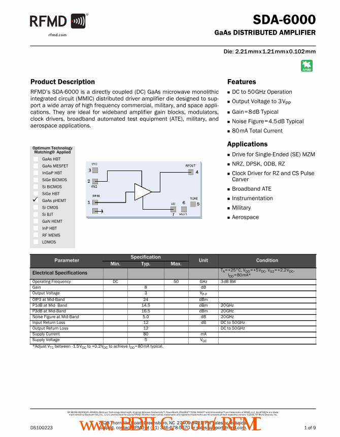
Features
1 of 9
Optimum Technology Matching ® Applied
GaAs HBT
InGaP HBT
GaAs MESFET
SiGe BiCMOS
Si BiCMOS
SiGe HBT
GaAs pHEMT
Si CMOS
Si BJT
GaN HEMT
RF MICRO DEVICES®, RFMD®, Optimum Technology Matching®, Enabling Wireless Connectivity™, PowerStar®, POLARIS™ TOTAL RADIO™ and UltimateBlue™ are trademarks of RFMD, LLC. BLUETOOTH is a trade-mark owned by Bluetooth SIG, Inc., U.S.A. and licensed for use by RFMD. All other trade names, trademarks and registered trademarks are the property of their respective owners. ©2006, RF Micro Devices, Inc.
Product Description
7628 Thorndike Road, Greensboro, NC 27409-9421 · For sales or technical support, contact RFMD at (+1) 336-678-5570 or [email protected].
InP HBT
LDMOS
RF MEMS
SDA-6000GaAs DISTRIBUTED AMPLIFIER
RFMD’s SDA-6000 is a directly coupled (DC) GaAs microwave monolithicintegrated circuit (MMIC) distributed driver amplifier die designed to sup-port a wide array of high frequency commercial, military, and space appli-cations. They are ideal for wideband amplifier gain blocks, modulators,clock drivers, broadband automated test equipment (ATE), military, andaerospace applications.
DC to 50 GHz Operation
Output Voltage to 3 VPP
Gain = 8 dB Typical
Noise Figure = 4.5 dB Typical
80 mA Total Current
Applications Drive for Single-Ended (SE) MZM
NRZ, DPSK, ODB, RZ
Clock Driver for RZ and CS Pulse Carver
Broadband ATE
Instrumentation
Military
Aerospace
DS100223
Die: 2.21 mm x 1.21 mm x 0.102 mm
SDA-6000GaAs Distrib-uted Amplifier
ParameterSpecification
Unit ConditionMin. Typ. Max.
Electrical Specifications TA = +25°C, VDD = +5 VDC, VG2 = +2.2 VDC, IDD = 80 mA*
Operating Frequency DC 50 GHz 3 dB BWGain 8 dBOutput Voltage 3 VP-P
OIP3 at Mid-Band 24 dBmP1dB at Mid- Band 14.5 dBm 20 GHzP3dB at Mid-Band 16.5 dBm 20 GHzNoise Figure at Mid-Band 5.0 dB 20 GHzInput Return Loss 12 dB DC to 50 GHzOutput Return Loss 12 DC to 50 GHzSupply Current 80 mASupply Voltage 5 VDC
*Adjust VT1 between -1.5 VDC to +0.2 VDC to achieve IDD = 80 mA typical.
www.BDTIC.com/RFMD
SDA-6000
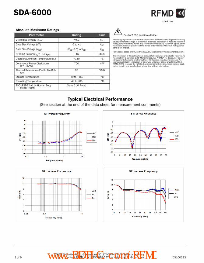
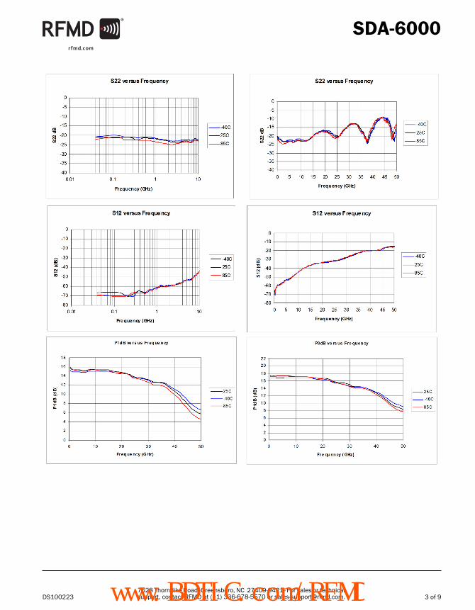
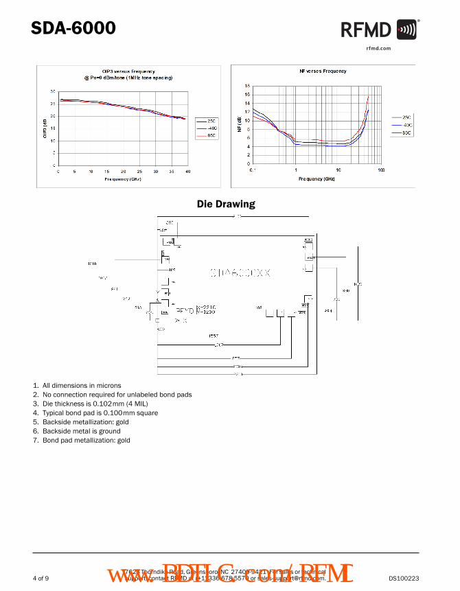
Typical Electrical Performance(See section at the end of the data sheet for measurement comments)
Absolute Maximum RatingsParameter Rating Unit
Drain Bias Voltage (VDD) +9.0 VDC
Gate Bias Voltage (VTI) -2 to +1 VDC
Gate Bias Voltage (VG2) (VDD - 5.0) to VDD VDC
RF Input Power (VDD = +8.0 VDC) +15 dBm
Operating Junction Temperature (TJ) +150 °C
Continuous Power Dissipation (T = +85°C)
700 mW
Thermal Resistance (Pad to Die Bot-tom)
93 °C/W
Storage Temperature -40 to +150 °C
Operating Temperature -40 to +85 °C
ESD JESD22-A114 Human Body Model (HBM)
Class 0 (All Pads)
Caution! ESD sensitive device.
Exceeding any one or a combination of the Absolute Maximum Rating conditions may cause permanent damage to the device. Extended application of Absolute Maximum Rating conditions to the device may reduce device reliability. Specified typical perfor-mance or functional operation of the device under Absolute Maximum Rating condi-tions is not implied.
RoHS status based on EU Directive 2002/95/EC (at time of this document revision).
The information in this publication is believed to be accurate and reliable. However, no responsibility is assumed by RF Micro Devices, Inc. ("RFMD") for its use, nor for any infringement of patents, or other rights of third parties, resulting from its use. No license is granted by implication or otherwise under any patent or patent rights of RFMD. RFMD reserves the right to change component circuitry, recommended appli-cation circuitry and specifications at any time without prior notice.
2 of 9 DS1002237628 Thorndike Road, Greensboro, NC 27409-9421 · For sales or technical support, contact RFMD at (+1) 336-678-5570 or [email protected]/RFMD
SDA-6000
3 of 9DS1002237628 Thorndike Road, Greensboro, NC 27409-9421 · For sales or technical support, contact RFMD at (+1) 336-678-5570 or [email protected]/RFMD
SDA-6000
Die Drawing
1. All dimensions in microns2. No connection required for unlabeled bond pads3. Die thickness is 0.102 mm (4 MIL)4. Typical bond pad is 0.100 mm square5. Backside metallization: gold6. Backside metal is ground7. Bond pad metallization: gold
4 of 9 DS1002237628 Thorndike Road, Greensboro, NC 27409-9421 · For sales or technical support, contact RFMD at (+1) 336-678-5570 or [email protected]/RFMD

SDA-6000
Bias Sequence (turn device on):
• VTI - Apply negative -2.0 volts. (This shuts the device off.)
• VG2 - Apply positive 2.2 volts.
• VDD - Apply positive 5.0 volts to the RF output bias tee.
• Important - Adjust VTI between -2 to +1 volts to achieve IDD = 80 mA nominal.
Bias Sequence (turn device off):
• VTI - Return to negative -2.0 volts.
• VDD - Remove positive 5.0 volts to the RF output bias tee.
• VG2 - Remove positive 2.2 volts.
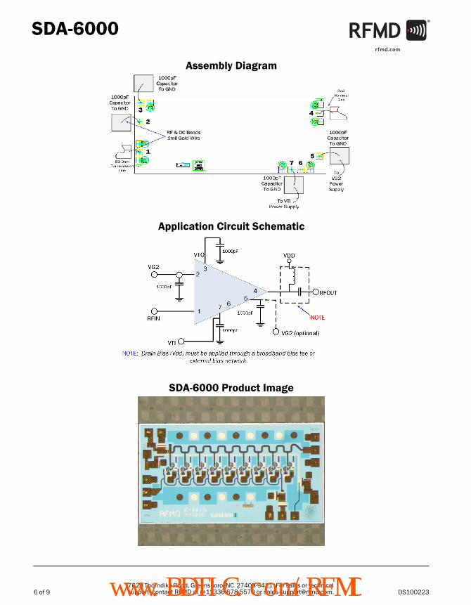
Pin Function Description Interface Schematic1 RFIN RF Input. This pad is DC coupled and matched to 50 from DC to 50 GHz. 50
microstrip transmission line on 0.127 mm (5 mil) thick alumina thin film sub-strate is recommended for RF input and output. A DC blocking capacitor is required for this connection. The calue of this capacitor will be based on the desired frequency range of application.
2 VG2 Each amplifier stage in the SDA-6OOO is a cascade configuration. The gate of each upper FET in the cascade amplifiers is biased with the 2.2 VDC supply men-tioned in this data sheet. The DC connection for the upper device gates runs across the length of the die. Pads 2 and 5 are both on this DC connection but are on opposite ends of the die. The 2.2 VDC connection can therefore be placed on either pad. A bypass capacitor is recommended on both ends, pads 2 and 5.
3 VTO The output drain termination pad. This pad requires a 1000 pF bypass capacitor with the shortest wirebond length to prevent low frequency gain ripple.
4 RFOUT and VDD
RF Output. 50 microstrip transmission line on 0.127 mm (5 mil) thick alumina thin film substrate is recommended for RF input and output. Connect the DC bias (VDD) network to provide drain current (IDD).Note: Drain Bias (VDD) must be applied through a broadband bias tee or external bias network.
5 VCAS Each amplifier stage in the SDA-6OOO is a cascade configuration. The gate of each upper FET in the cascade amplifiers is biased with the 2.2 VDC supply men-tioned in this data sheet. The DC connection for the upper device gates runs across the length of the die. Pads 2 and 5 are both on this DC connection but are on opposite ends of the die. The 2.2 VDC connection can therefore be placed on either pad. A bypass capacitor is recommended on both ends, pads 2 and 5.
6 VG21 Not connected.
7 VTI Input gate voltage for the lower devices in the cascade amplifier. This pad also serves as the RF ground for the input termination resistor. The DC voltage applied to this pad will be between -2 VDC (device is pinched OFF) to +1 VDC (fully ON). The value of this capacitor will effect the low frequency response of the amplifier.
Die GND Ground connection. Connect die bottom directly to ground plane for best perfor-mance. NOTE: The die should be connected directly to the ground plane with con-ductive epoxy.
5 of 9DS1002237628 Thorndike Road, Greensboro, NC 27409-9421 · For sales or technical support, contact RFMD at (+1) 336-678-5570 or [email protected]/RFMD
SDA-6000
Assembly Diagram
Application Circuit Schematic
SDA-6000 Product Image
6 of 9 DS1002237628 Thorndike Road, Greensboro, NC 27409-9421 · For sales or technical support, contact RFMD at (+1) 336-678-5570 or [email protected]/RFMD
SDA-6000
Measurement TechniqueAll data presented in this document represents the integrated circuit and accompanying bond wires.
All performance data reported in this document were measured in the following manner. Data was taken using a temperaturecontrolled probe station utilizing 150 μm pitch GSG probes. The interface between the probes and integrated circuit was madewith a coplanar to microstrip ceramic test interface. The test interface was wire bonded to the die using 1 mil diameter bond-wires. The spacing between the test interface and the die was 200 μm, and the bond wire loop height was 100 μm. The calibra-tion of the test fixture included the probes and test interfaces, so that the measurement reference plane was at the point ofbond wire attachment to the ceramic interface. The presented data therefore represents the chip plus wirebonds.
Ordering InformationPart Number Description Delivery Method Die/GelPak
SDA-6000 GaAs Distributed Amplifier, 40 GHz, 2.4 mm x 1.20 mm Die
GelPak 10 or more
SDA-6000SB Sample Bag, GaAs Distributed Amplifier, 40 GHz, 2.4 mm x 1.2 mm Die
GelPak 2
7 of 9DS1002237628 Thorndike Road, Greensboro, NC 27409-9421 · For sales or technical support, contact RFMD at (+1) 336-678-5570 or [email protected]/RFMD
SDA-6000
8 of 9 DS1002237628 Thorndike Road, Greensboro, NC 27409-9421 · For sales or technical support, contact RFMD at (+1) 336-678-5570 or [email protected]/RFMD
SDA-6000
9 of 9DS1002237628 Thorndike Road, Greensboro, NC 27409-9421 · For sales or technical support, contact RFMD at (+1) 336-678-5570 or [email protected]/RFMD