Embed Size (px)
Citation preview
2
Capping of InAs/GaAs Quantum Dots for GaAs Based Lasers
Alice Hospodková Institute of Physics AS CR, v. v. i., Prague
Czech Republic
1. Introduction
Nowadays, self-assembled InAs quantum dots grown on GaAs substrates are intensively studied due to their potential applications: quantum dot ensembles are employed in laser active regions and mid-infrared detectors, single quantum dots have a potential for application in memories, two-level information processing or single photon sources (Henini& Bugajski, 2005; Mowbray& Skolnick, 2005; Battacharya, 2007).
This chapter is concentrated on quantum dots, which are prepared with the aim to become a base for low cost, low threshold, high output and heat sink free lasers for the 1.3 or even 1.55 µm communication band. To be embedded in a functional structure, dots must be covered by a capping layer. Capping of quantum dots is currently a very important topic of research (Bozkhurt et al., 2011; Dasika et al., 2009; Haxha et al., 2009; Kong et al., 2008). The overgrowth process is essential to obtain dot parameters necessary for the realization of novel optoelectronic devices. This chapter is a kind of review report on the structural and optical changes during the process of capping of self-assembled InAs quantum dots. The presented results are measured on samples grown by metal-organic vapour phase epitaxy which is the growth technique of choice for high volume laser production.
Growth conditions of InAs/GaAs quantum dot layer determine such parameters as density, homogeneity and original size of quantum dots. However, the final properties of quantum dots are significantly determined by quantum dot capping, since during the capping process the redistribution of In atoms takes place. This decreases the height of dots and changes their shape. The published and our results show that the GaAs capping layer transforms originally circular lens shaped quantum dots into elongated objects and their height is significantly decreased. The strain field surrounding dots is also changed during the capping process and can be influenced by the composition and the thickness of the layers grown above quantum dots.
The aim of the chapter is to elucidate the processes during the dot capping by reflectance anisotropy spectroscopy in situ measurements and to discuss the influence of the capping layer composition and thickness on the structural and optical properties of InAs/GaAs quantum dots. Three most common types of capping layers are studied: simple GaAs capping layer, InGaAs and GaAsSb. The emission wavelength of quantum dots capped by GaAs is usually around 1200 nm, which is not interesting for application in telecommunication devices, since they need to be operated at wavelengths 1300 or 1550 nm
www.intechopen.com
Quantum Dots – A Variety of New Applications
28
to minimize the losses in optical waveguides. One way to redshift the emission wavelength is to increase the size of dots by increasing the amount of deposited InAs (Krzyzewski et al., 2002), by controlling growth conditions (especially increasing temperature) (Johanson et al., 2002), by growth on high index surfaces (Akijama et al., 2007) or by growing multiple quantum dot structures (Hospodkova et al., 2008). Another way to shift emission wavelength is to cap dots by so called strain reducing layers. The lattice constant of the strain reducing material is bigger than that for GaAs substrate but smaller than lattice constant of the dot material (InAs or InGaAs). The redshift is then caused by combined effect of reduced strain inside quantum dots, increased dot aspect ratio and decreased bandgap of the capping barrier material. Materials most often used for the strain reduction are InGaAs and GaAsSb. Advantages and disadvantages of both types of strain reducing layers are discussed in section 3. The longest achieved electroluminescence wavelength of 1520 nm was recently reported by (Majid et al., 2011, a, b). This unique result was achieved by combination of bilayer structure with InGaAs strain reducing capping layer. The structure was grown by molecular beam epitaxy.
More than one quantum dot layer are required in lasers to increase the gain. In such a case the capping layer serves also as a separating layer between two quantum dot layers. During the growth of the separation layers, surfactant atoms like In have to be removed from epitaxial surface, so that the In is not transported from one quantum dot layer to the following one. Different types of In flushing method during the growth of capping layers and their importance are discussed at the end of the chapter in section 4.
The photoluminescence or electroluminescence and reflectance anisotropy spectroscopy as in situ monitoring of the technological process are the main methods which help us to evaluate the quantum dot properties, supporting methods are atomic force microscopy of quantum dot surface, transmission electron microscopy, X-ray diffraction used to determine the composition of the ternary capping layers and X-ray reflection used for capping layer thickness evaluation.
2. GaAs capping
Combination of InAs and GaAs layers forms highly mismatched heterostructure (7% mismatch of lattice constants). This mismatch is a driving force for Stranski-Krastanow quantum dot formation. Dots are formed to decrease the strain in deposited InAs material. The lowest strain occurs at the apex of quantum dot. On the other hand the strain in the structure complicates the quantum dot preparation, since accumulated strain energy can lead to the formation of dislocations in the structure for oversized dots or in the case of more quantum dot layers.
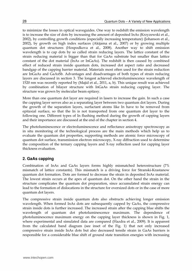
The compressive strain inside quantum dots also obstructs achieving longer emission wavelength. When formed InAs dots are subsequently capped by GaAs, the compressive strain inside dots is further increased. The increased strain after the capping blue shifts the wavelength of quantum dot photoluminescence maximum. The dependence of photoluminescence maximum energy on the capping layer thickness is shown in Fig. 1, where experimental and simulated data are compared (Hazdra et al., 2009). It is apparent from the calculated band diagram (see inset of the Fig. 1) that not only increased compressive strain inside InAs dots but also decreased tensile strain in GaAs barriers is responsible for a considerable blue shift of ground state transition energies with increasing
www.intechopen.com
Capping of InAs/GaAs Quantum Dots for GaAs Based Lasers
29
capping thickness. More detailed study of the impact of the capping layer thickness on the electronic structure of quantum dots can be found in (Wu et al., 2006).
Fig. 1. Comparison of measured (photoluminescence - circles) and calculated (diamonds) room temperature transition energies originating from InAs quantum dots covered with GaAs capping layers with different thickness. The corresponding band diagrams (taken in the quantum dot centre along the [001] axis) are shown in the inset (Hazdra et al., 2009, a).
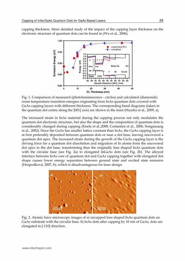
The increased strain in InAs material during the capping process not only modulates the quantum dot electronic structure, but also the shape and the composition of quantum dots is considerably changed during capping (Eisele et al.,2008; Costantini et al., 2006; Songmuang et al., 2002). Since the GaAs has smaller lattice constant than InAs, the GaAs capping layer is at first preferably deposited between quantum dots or near a dot base, leaving uncovered a quantum dot apex. The increased strain during the growth of the GaAs capping layer is the driving force for a quantum dot dissolution and migration of In atoms from the uncovered dot apex to the dot base, transforming thus the originally lens shaped InAs quantum dots with the circular base (see Fig. 2a) to elongated InGaAs dots (see Fig. 2b). The alloyed interface between InAs core of quantum dot and GaAs capping together with elongated dot shape causes lower energy separation between ground state and excited state emission (Hospodková, 2007, b), which is disadvantageous for laser design.
200nm
200nm
Fig. 2. Atomic force microscopy images of a) uncapped lens shaped InAs quantum dots on GaAs substrate with the circular base. b) InAs dots after capping by 10 nm of GaAs, dots are elongated in [-110] direction.
a) b)
www.intechopen.com
Quantum Dots – A Variety of New Applications
30
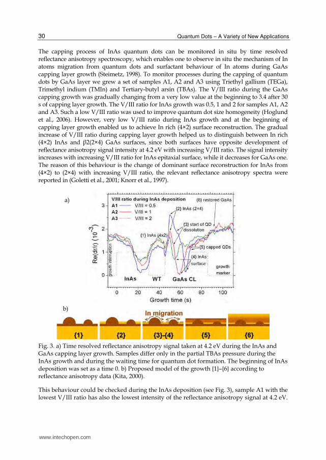
The capping process of InAs quantum dots can be monitored in situ by time resolved reflectance anisotropy spectroscopy, which enables one to observe in situ the mechanism of In atoms migration from quantum dots and surfactant behaviour of In atoms during GaAs capping layer growth (Steimetz, 1998). To monitor processes during the capping of quantum dots by GaAs layer we grew a set of samples A1, A2 and A3 using Triethyl gallium (TEGa), Trimethyl indium (TMIn) and Tertiary-butyl arsin (TBAs). The V/III ratio during the GaAs capping growth was gradually changing from a very low value at the beginning to 3.4 after 30 s of capping layer growth. The V/III ratio for InAs growth was 0.5, 1 and 2 for samples A1, A2 and A3. Such a low V/III ratio was used to improve quantum dot size homogeneity (Hoglund et al., 2006). However, very low V/III ratio during InAs growth and at the beginning of capping layer growth enabled us to achieve In rich (4×2) surface reconstruction. The gradual increase of V/III ratio during capping layer growth helped us to distinguish between In rich (4×2) InAs and β2(2×4) GaAs surfaces, since both surfaces have opposite development of reflectance anisotropy signal intensity at 4.2 eV with increasing V/III ratio. The signal intensity increases with increasing V/III ratio for InAs epitaxial surface, while it decreases for GaAs one. The reason of this behaviour is the change of dominant surface reconstruction for InAs from (4×2) to (2×4) with increasing V/III ratio, the relevant reflectance anisotropy spectra were reported in (Goletti et al., 2001; Knorr et al., 1997).
Fig. 3. a) Time resolved reflectance anisotropy signal taken at 4.2 eV during the InAs and GaAs capping layer growth. Samples differ only in the partial TBAs pressure during the InAs growth and during the waiting time for quantum dot formation. The beginning of InAs deposition was set as a time 0. b) Proposed model of the growth {1}–{6} according to reflectance anisotropy data (Kita, 2000).
This behaviour could be checked during the InAs deposition (see Fig. 3), sample A1 with the lowest V/III ratio has also the lowest intensity of the reflectance anisotropy signal at 4.2 eV.
a)
b)
www.intechopen.com
Capping of InAs/GaAs Quantum Dots for GaAs Based Lasers
31
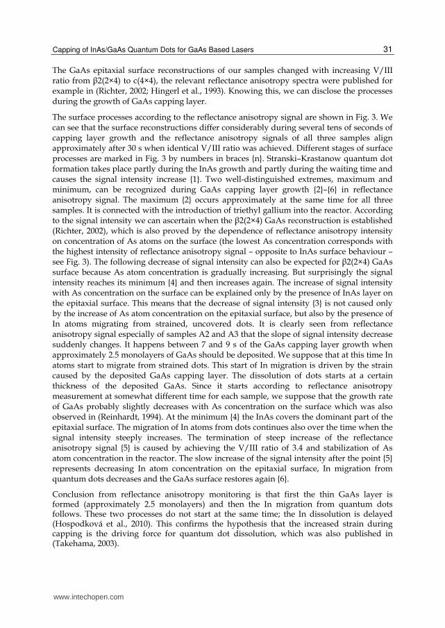
The GaAs epitaxial surface reconstructions of our samples changed with increasing V/III ratio from β2(2×4) to c(4×4), the relevant reflectance anisotropy spectra were published for example in (Richter, 2002; Hingerl et al., 1993). Knowing this, we can disclose the processes during the growth of GaAs capping layer.
The surface processes according to the reflectance anisotropy signal are shown in Fig. 3. We can see that the surface reconstructions differ considerably during several tens of seconds of capping layer growth and the reflectance anisotropy signals of all three samples align approximately after 30 s when identical V/III ratio was achieved. Different stages of surface processes are marked in Fig. 3 by numbers in braces {n}. Stranski–Krastanow quantum dot formation takes place partly during the InAs growth and partly during the waiting time and causes the signal intensity increase {1}. Two well-distinguished extremes, maximum and minimum, can be recognized during GaAs capping layer growth {2}–{6} in reflectance anisotropy signal. The maximum {2} occurs approximately at the same time for all three samples. It is connected with the introduction of triethyl gallium into the reactor. According to the signal intensity we can ascertain when the β2(2×4) GaAs reconstruction is established (Richter, 2002), which is also proved by the dependence of reflectance anisotropy intensity on concentration of As atoms on the surface (the lowest As concentration corresponds with the highest intensity of reflectance anisotropy signal – opposite to InAs surface behaviour – see Fig. 3). The following decrease of signal intensity can also be expected for β2(2×4) GaAs surface because As atom concentration is gradually increasing. But surprisingly the signal intensity reaches its minimum {4} and then increases again. The increase of signal intensity with As concentration on the surface can be explained only by the presence of InAs layer on the epitaxial surface. This means that the decrease of signal intensity {3} is not caused only by the increase of As atom concentration on the epitaxial surface, but also by the presence of In atoms migrating from strained, uncovered dots. It is clearly seen from reflectance anisotropy signal especially of samples A2 and A3 that the slope of signal intensity decrease suddenly changes. It happens between 7 and 9 s of the GaAs capping layer growth when approximately 2.5 monolayers of GaAs should be deposited. We suppose that at this time In atoms start to migrate from strained dots. This start of In migration is driven by the strain caused by the deposited GaAs capping layer. The dissolution of dots starts at a certain thickness of the deposited GaAs. Since it starts according to reflectance anisotropy measurement at somewhat different time for each sample, we suppose that the growth rate of GaAs probably slightly decreases with As concentration on the surface which was also observed in (Reinhardt, 1994). At the minimum {4} the InAs covers the dominant part of the epitaxial surface. The migration of In atoms from dots continues also over the time when the signal intensity steeply increases. The termination of steep increase of the reflectance anisotropy signal {5} is caused by achieving the V/III ratio of 3.4 and stabilization of As atom concentration in the reactor. The slow increase of the signal intensity after the point {5} represents decreasing In atom concentration on the epitaxial surface, In migration from quantum dots decreases and the GaAs surface restores again {6}.
Conclusion from reflectance anisotropy monitoring is that first the thin GaAs layer is formed (approximately 2.5 monolayers) and then the In migration from quantum dots follows. These two processes do not start at the same time; the In dissolution is delayed (Hospodková et al., 2010). This confirms the hypothesis that the increased strain during capping is the driving force for quantum dot dissolution, which was also published in (Takehama, 2003).
www.intechopen.com
Quantum Dots – A Variety of New Applications
32
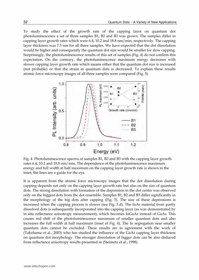
To study the effect of the growth rate of the capping layer on quantum dot
photoluminescence a set of three samples B1, B2 and B3 was grown. The samples differ in
capping layer growth rates which were 6.4, 10.2 and 18.8 nm/min, respectively. The capping
layer thickness was 7.5 nm for all three samples. We have expected that the dot dissolution
would be higher and consequently the quantum dot size would be smaller for slow capping.
Surprisingly, the photoluminescence results of this set of samples (Fig. 4) do not confirm this
expectation. On the contrary, the photoluminescence maximum energy decreases with
slower capping layer growth rate which means either that the quantum dot size is increased
(not probable) or that the strain in quantum dots is decreased. To explain these results
atomic force microscopy images of all three samples were compared (Fig. 5).
Fig. 4. Photoluminescence spectra of samples B1, B2 and B3 with the capping layer growth rates 6.4, 10.2 and 18.8 nm/min. The dependence of the photoluminescence maximum energy and full width at half maximum on the capping layer growth rate is shown in the inset; the lines are a guide for the eye.
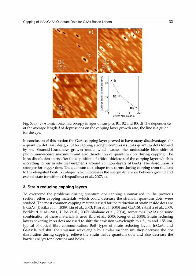
It is apparent from the atomic force microscopy images that the dot dissolution during
capping depends not only on the capping layer growth rate but also on the size of quantum
dots. The strong dissolution with formation of the depression in the dot centre was observed
only on the biggest dots from the dot ensemble. Samples B1, B2 and B3 differ significantly in
the morphology of the big dots after capping (Fig. 5). The size of these depressions is
increased when the capping process is slower (see Fig. 5.d). The InAs material from partly
dissolved dots is subsequently incorporated into the capping layer (as was demonstrated by
in situ reflectance anisotropy measurement), which becomes InGaAs instead of GaAs. This
causes red shift of the photoluminescence maximum of smaller quantum dots and also
increases the full width at half maximum (inset of Fig. 4). The In segregation near smaller
quantum dots cannot be excluded. These results are in agreement with the work of
(Takehama et al., 2003) who has studied the influence of the GaAs capping layer thickness
on quantum dot morphology. The stronger dissolution of bigger dots can be also deduced
from reflectance anisotropy results presented in (Steimetz et al., 1998).
www.intechopen.com
Capping of InAs/GaAs Quantum Dots for GaAs Based Lasers
33
Fig. 5. a) - c) Atomic force microscopy images of samples B1, B2 and B3. d) The dependence of the average length d of depressions on the capping layer growth rate, the line is a guide for the eye.
In conclusion of this section the GaAs capping layer proved to have many disadvantages for a quantum dot laser design. GaAs capping strongly compresses InAs quantum dots formed by the Stranski-Krastanow growth mode, which causes the undesirable blue shift of photoluminescence maximum and also dissolution of quantum dots during capping. The InAs dissolution starts after the deposition of critical thickness of the capping layer which is according to our in situ measurements around 2.5 monolayers of GaAs. The dissolution is stronger for bigger dots. The quantum dots shape transforms during capping from the lens to the elongated boat-like shape, which decreases the energy difference between ground and excited state transitions (Hospodkova et al., 2007, a).
3. Strain reducing capping layers
To overcome the problems during quantum dot capping summarized in the previous section, other capping materials, which could decrease the strain in quantum dots, were studied. The most common capping materials used for the reduction of strain inside dots are InGaAs (Dasika et al., 2009; Liu et al., 2003; Kim et al., 2003) and GaAsSb (Haxha et al., 2009; Bozkhurt et al., 2011; Ulloa et al., 2007; Akahane et al., 2004), sometimes InAlAs or some combination of these materials is used (Liu et al., 2005; Kong et al.,2008). Strain reducing layers covering InAs dots are used to shift the emission wavelength to 1.3 µm and 1.55 µm, typical of optical fibre communication. Both types of strain reducing layers, InGaAs and GaAsSb, red shift the emission wavelength by similar mechanism: they decrease the dot dissolution during capping, relieve the strain inside quantum dots and also decrease the barrier energy for electrons and holes.
www.intechopen.com
Quantum Dots – A Variety of New Applications
34
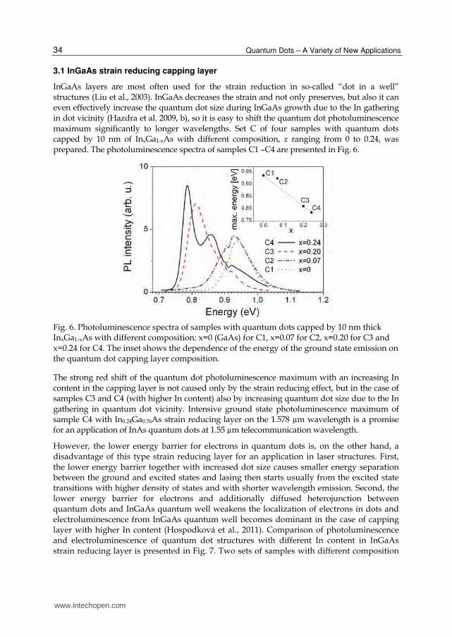
3.1 InGaAs strain reducing capping layer
InGaAs layers are most often used for the strain reduction in so-called “dot in a well” structures (Liu et al., 2003). InGaAs decreases the strain and not only preserves, but also it can even effectively increase the quantum dot size during InGaAs growth due to the In gathering in dot vicinity (Hazdra et al. 2009, b), so it is easy to shift the quantum dot photoluminescence maximum significantly to longer wavelengths. Set C of four samples with quantum dots capped by 10 nm of InxGa1-xAs with different composition, x ranging from 0 to 0.24, was prepared. The photoluminescence spectra of samples C1 –C4 are presented in Fig. 6.
Fig. 6. Photoluminescence spectra of samples with quantum dots capped by 10 nm thick InxGa1-xAs with different composition: x=0 (GaAs) for C1, x=0.07 for C2, x=0.20 for C3 and x=0.24 for C4. The inset shows the dependence of the energy of the ground state emission on the quantum dot capping layer composition.
The strong red shift of the quantum dot photoluminescence maximum with an increasing In content in the capping layer is not caused only by the strain reducing effect, but in the case of samples C3 and C4 (with higher In content) also by increasing quantum dot size due to the In gathering in quantum dot vicinity. Intensive ground state photoluminescence maximum of sample C4 with In0.24Ga0.76As strain reducing layer on the 1.578 µm wavelength is a promise for an application of InAs quantum dots at 1.55 µm telecommunication wavelength.
However, the lower energy barrier for electrons in quantum dots is, on the other hand, a disadvantage of this type strain reducing layer for an application in laser structures. First, the lower energy barrier together with increased dot size causes smaller energy separation between the ground and excited states and lasing then starts usually from the excited state transitions with higher density of states and with shorter wavelength emission. Second, the lower energy barrier for electrons and additionally diffused heterojunction between quantum dots and InGaAs quantum well weakens the localization of electrons in dots and electroluminescence from InGaAs quantum well becomes dominant in the case of capping layer with higher In content (Hospodková et al., 2011). Comparison of photoluminescence and electroluminescence of quantum dot structures with different In content in InGaAs strain reducing layer is presented in Fig. 7. Two sets of samples with different composition
www.intechopen.com
Capping of InAs/GaAs Quantum Dots for GaAs Based Lasers
35
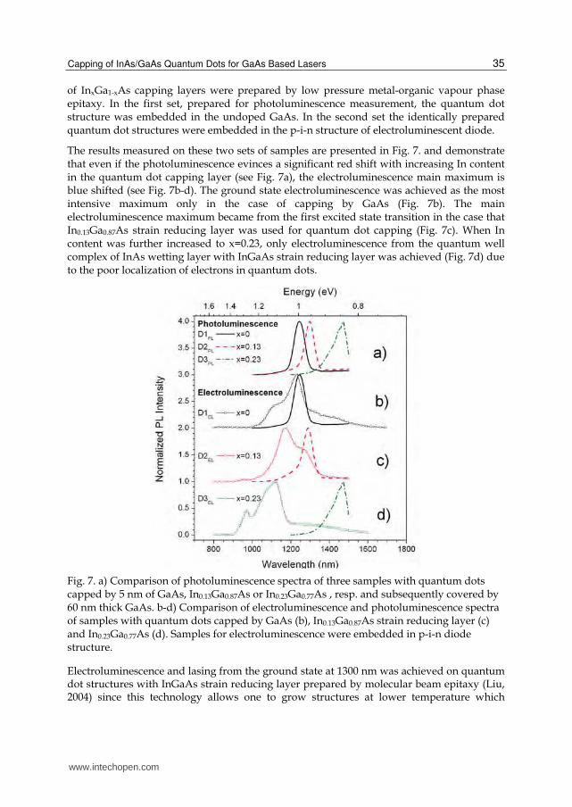
of InxGa1-xAs capping layers were prepared by low pressure metal-organic vapour phase epitaxy. In the first set, prepared for photoluminescence measurement, the quantum dot structure was embedded in the undoped GaAs. In the second set the identically prepared quantum dot structures were embedded in the p-i-n structure of electroluminescent diode.
The results measured on these two sets of samples are presented in Fig. 7. and demonstrate that even if the photoluminescence evinces a significant red shift with increasing In content in the quantum dot capping layer (see Fig. 7a), the electroluminescence main maximum is blue shifted (see Fig. 7b-d). The ground state electroluminescence was achieved as the most intensive maximum only in the case of capping by GaAs (Fig. 7b). The main electroluminescence maximum became from the first excited state transition in the case that In0.13Ga0.87As strain reducing layer was used for quantum dot capping (Fig. 7c). When In content was further increased to x=0.23, only electroluminescence from the quantum well complex of InAs wetting layer with InGaAs strain reducing layer was achieved (Fig. 7d) due to the poor localization of electrons in quantum dots.
Fig. 7. a) Comparison of photoluminescence spectra of three samples with quantum dots capped by 5 nm of GaAs, In0.13Ga0.87As or In0.23Ga0.77As , resp. and subsequently covered by 60 nm thick GaAs. b-d) Comparison of electroluminescence and photoluminescence spectra of samples with quantum dots capped by GaAs (b), In0.13Ga0.87As strain reducing layer (c) and In0.23Ga0.77As (d). Samples for electroluminescence were embedded in p-i-n diode structure.
Electroluminescence and lasing from the ground state at 1300 nm was achieved on quantum dot structures with InGaAs strain reducing layer prepared by molecular beam epitaxy (Liu, 2004) since this technology allows one to grow structures at lower temperature which
www.intechopen.com
Quantum Dots – A Variety of New Applications
36
decrease the In segregation and diffusion and improves localization of electrons in quantum dots. The localization of electrons in dots can be further improved by graded composition of InGaAs (Kim, 2003) or by combining the InGaAs strain reducing layer with InAlAs (Kong, 2008). Unfortunately, graded InGaAs composition is difficult to achieve when metal-organic vapour phase epitaxy is used for structure growth due to high In segregation during capping (Steimetz, 1998). Also the combination of InGaAs with InAlAs cannot be used by this technology because of the high decomposition temperature of available Al precursors. So the InGaAs is not suitable strain reducing layer for quantum dot structures prepared by metal-organic vapour phase epitaxy.
3.2 GaAsSb strain reducing capping layer
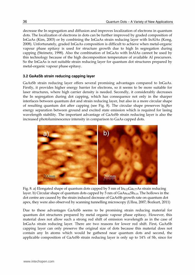
GaAsSb strain reducing layer offers several promising advantages compared to InGaAs. Firstly, it provides higher energy barrier for electrons, so it seems to be more suitable for laser structures, where high carrier density is needed. Secondly, it considerably decreases the In segregation during dot capping, which has consequence not only in the sharper interfaces between quantum dot and strain reducing layer, but also in a more circular shape of resulting quantum dot after capping (see Fig. 8). The circular shape preserves higher energy separation between ground and excited state emission which is required for lasing wavelength stability. The important advantage of GaAsSb strain reducing layer is also the increased photoluminescence intensity in comparison to GaAs capped dots.
Fig. 8. a) Elongated shape of quantum dots capped by 5 nm of In0.23Ga0.77As strain reducing layer. b) Circular shape of quantum dots capped by 5 nm of GaAs0.81Sb0.19. The hollows in the dot centre are caused by the strain induced decrease of GaAsSb growth rate on quantum dot apex, they were also observed by scanning tunnelling microscopy (Ulloa, 2007; Bozkurt, 2011)
Due to these advantages GaAsSb seems to be promising strain reducing material for quantum dot structures prepared by metal organic vapour phase epitaxy. However, this material does not allow such a strong red shift of emission wavelength as in the case of InGaAs strain reducing layer. There are two reasons for lower red shift. First, GaAsSb capping layer can only preserve the original size of dots because this material does not contain any In atoms which would be gathered near quantum dots and second, the applicable composition of GaAsSb strain reducing layer is only up to 14% of Sb, since for
www.intechopen.com
Capping of InAs/GaAs Quantum Dots for GaAs Based Lasers
37
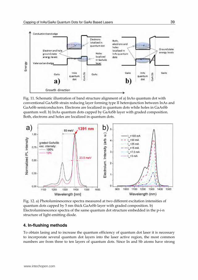
higher Sb content the heterostructure becomes type II with holes confined in GaAsSb quantum well and electrons localized in quantum dots (see Fig. 11a). The emission intensity decreases significantly for type II heterostructure due to the worse overlap of electron and hole wave functions.
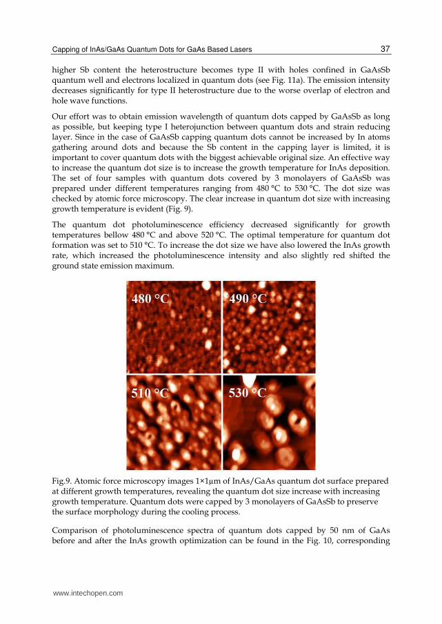
Our effort was to obtain emission wavelength of quantum dots capped by GaAsSb as long as possible, but keeping type I heterojunction between quantum dots and strain reducing layer. Since in the case of GaAsSb capping quantum dots cannot be increased by In atoms gathering around dots and because the Sb content in the capping layer is limited, it is important to cover quantum dots with the biggest achievable original size. An effective way to increase the quantum dot size is to increase the growth temperature for InAs deposition. The set of four samples with quantum dots covered by 3 monolayers of GaAsSb was prepared under different temperatures ranging from 480 °C to 530 °C. The dot size was checked by atomic force microscopy. The clear increase in quantum dot size with increasing growth temperature is evident (Fig. 9).
The quantum dot photoluminescence efficiency decreased significantly for growth temperatures bellow 480 °C and above 520 °C. The optimal temperature for quantum dot formation was set to 510 °C. To increase the dot size we have also lowered the InAs growth rate, which increased the photoluminescence intensity and also slightly red shifted the ground state emission maximum.
Fig.9. Atomic force microscopy images 1×1µm of InAs/GaAs quantum dot surface prepared at different growth temperatures, revealing the quantum dot size increase with increasing growth temperature. Quantum dots were capped by 3 monolayers of GaAsSb to preserve the surface morphology during the cooling process.
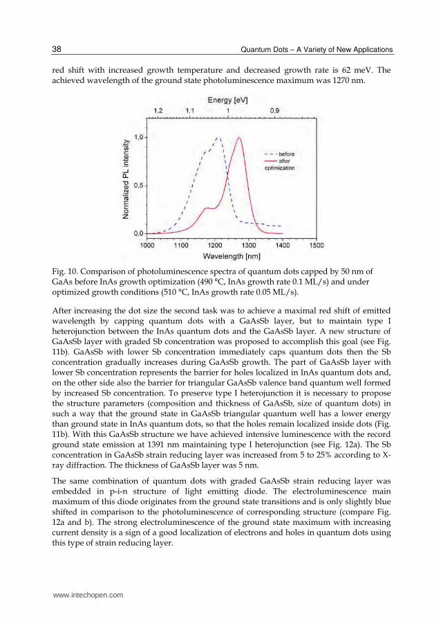
Comparison of photoluminescence spectra of quantum dots capped by 50 nm of GaAs before and after the InAs growth optimization can be found in the Fig. 10, corresponding
www.intechopen.com
Quantum Dots – A Variety of New Applications
38
red shift with increased growth temperature and decreased growth rate is 62 meV. The achieved wavelength of the ground state photoluminescence maximum was 1270 nm.
Fig. 10. Comparison of photoluminescence spectra of quantum dots capped by 50 nm of GaAs before InAs growth optimization (490 °C, InAs growth rate 0.1 ML/s) and under optimized growth conditions (510 °C, InAs growth rate 0.05 ML/s).
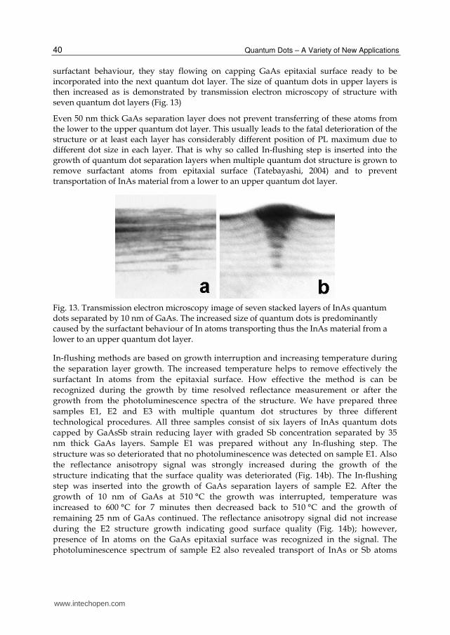
After increasing the dot size the second task was to achieve a maximal red shift of emitted wavelength by capping quantum dots with a GaAsSb layer, but to maintain type I heterojunction between the InAs quantum dots and the GaAsSb layer. A new structure of GaAsSb layer with graded Sb concentration was proposed to accomplish this goal (see Fig. 11b). GaAsSb with lower Sb concentration immediately caps quantum dots then the Sb concentration gradually increases during GaAsSb growth. The part of GaAsSb layer with lower Sb concentration represents the barrier for holes localized in InAs quantum dots and, on the other side also the barrier for triangular GaAsSb valence band quantum well formed by increased Sb concentration. To preserve type I heterojunction it is necessary to propose the structure parameters (composition and thickness of GaAsSb, size of quantum dots) in such a way that the ground state in GaAsSb triangular quantum well has a lower energy than ground state in InAs quantum dots, so that the holes remain localized inside dots (Fig. 11b). With this GaAsSb structure we have achieved intensive luminescence with the record ground state emission at 1391 nm maintaining type I heterojunction (see Fig. 12a). The Sb concentration in GaAsSb strain reducing layer was increased from 5 to 25% according to X-ray diffraction. The thickness of GaAsSb layer was 5 nm.
The same combination of quantum dots with graded GaAsSb strain reducing layer was embedded in p-i-n structure of light emitting diode. The electroluminescence main maximum of this diode originates from the ground state transitions and is only slightly blue shifted in comparison to the photoluminescence of corresponding structure (compare Fig. 12a and b). The strong electroluminescence of the ground state maximum with increasing current density is a sign of a good localization of electrons and holes in quantum dots using this type of strain reducing layer.
www.intechopen.com
Capping of InAs/GaAs Quantum Dots for GaAs Based Lasers
39
Fig. 11. Schematic illustration of band structure alignment of a) InAs quantum dot with conventional GaAsSb strain reducing layer forming type II heterojunction between InAs and GaAsSb semiconductors. Electrons are localized in quantum dots while holes in GaAsSb quantum well. b) InAs quantum dots capped by GaAsSb layer with graded composition. Both, electrons and holes are localized in quantum dots.
Fig. 12. a) Photoluminescence spectra measured at two different excitation intensities of quantum dots capped by 5 nm thick GaAsSb layer with graded composition. b) Electroluminescence spectra of the same quantum dot structure embedded in the p-i-n structure of light emitting diode.
4. In-flushing methods
To obtain lasing and to increase the quantum efficiency of quantum dot laser it is necessary to incorporate several quantum dot layers into the laser active region, the most common numbers are from three to ten layers of quantum dots. Since In and Sb atoms have strong
www.intechopen.com
Quantum Dots – A Variety of New Applications
40
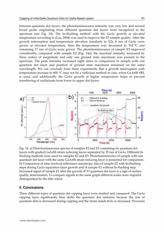
surfactant behaviour, they stay flowing on capping GaAs epitaxial surface ready to be incorporated into the next quantum dot layer. The size of quantum dots in upper layers is then increased as is demonstrated by transmission electron microscopy of structure with seven quantum dot layers (Fig. 13)
Even 50 nm thick GaAs separation layer does not prevent transferring of these atoms from the lower to the upper quantum dot layer. This usually leads to the fatal deterioration of the structure or at least each layer has considerably different position of PL maximum due to different dot size in each layer. That is why so called In-flushing step is inserted into the growth of quantum dot separation layers when multiple quantum dot structure is grown to remove surfactant atoms from epitaxial surface (Tatebayashi, 2004) and to prevent transportation of InAs material from a lower to an upper quantum dot layer.
Fig. 13. Transmission electron microscopy image of seven stacked layers of InAs quantum dots separated by 10 nm of GaAs. The increased size of quantum dots is predominantly caused by the surfactant behaviour of In atoms transporting thus the InAs material from a lower to an upper quantum dot layer.
In-flushing methods are based on growth interruption and increasing temperature during
the separation layer growth. The increased temperature helps to remove effectively the
surfactant In atoms from the epitaxial surface. How effective the method is can be
recognized during the growth by time resolved reflectance measurement or after the
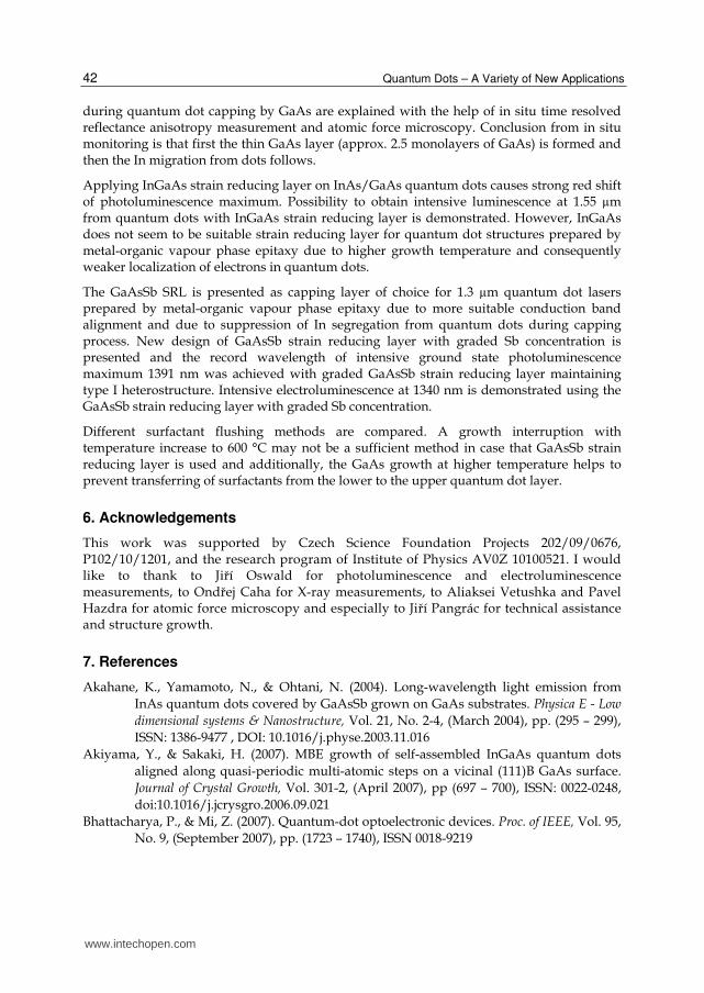
growth from the photoluminescence spectra of the structure. We have prepared three
samples E1, E2 and E3 with multiple quantum dot structures by three different
technological procedures. All three samples consist of six layers of InAs quantum dots
capped by GaAsSb strain reducing layer with graded Sb concentration separated by 35
nm thick GaAs layers. Sample E1 was prepared without any In-flushing step. The
structure was so deteriorated that no photoluminescence was detected on sample E1. Also
the reflectance anisotropy signal was strongly increased during the growth of the
structure indicating that the surface quality was deteriorated (Fig. 14b). The In-flushing
step was inserted into the growth of GaAs separation layers of sample E2. After the
growth of 10 nm of GaAs at 510 °C the growth was interrupted, temperature was
increased to 600 °C for 7 minutes then decreased back to 510 °C and the growth of
remaining 25 nm of GaAs continued. The reflectance anisotropy signal did not increase
during the E2 structure growth indicating good surface quality (Fig. 14b); however,
presence of In atoms on the GaAs epitaxial surface was recognized in the signal. The
photoluminescence spectrum of sample E2 also revealed transport of InAs or Sb atoms
www.intechopen.com
Capping of InAs/GaAs Quantum Dots for GaAs Based Lasers
41
between quantum dot layers, the photoluminescence intensity was very low and several
broad peaks originating from different quantum dot layers were recognized in the
spectrum (see Fig. 14). The In-flushing method with the GaAs growth at elevated
temperature according to (Liu, 2004) was used to improve the E3 sample quality. After the
growth interruption and temperature elevation (similarly to E2), 8 nm of GaAs were
grown at elevated temperature, then the temperature was decreased to 510 °C and
remaining 17 nm of GaAs were grown. The photoluminescence of sample E3 improved
considerably compared with sample E2 (Fig. 14a), the maximal intensity increased by
three orders of magnitude and only one ground state maximum was present in the
spectrum. The peak intensity increased eight times in comparison to sample with one
quantum dot layer and position of ground state maximum remained on the same
wavelength. We can conclude from these experiments that a growth interruption with
temperature increase to 600 °C may not be a sufficient method in case, when GaAsSb SRL
is used, and additionally the GaAs growth at higher temperature helps to prevent
transferring of surfactants from lower to upper dot layers.
Fig. 14. a) Photoluminescence spectra of samples E2 and E3 containing six quantum dot layers with graded GaAsSb strain reducing layers separated by 35 nm of GaAs. Different In flushing methods were used for samples E2 and E3. Photoluminescence of sample with one quantum dot layer with the same GaAsSb strain reducing layer is presented for comparison. b) Comparison of time resolved reflectance anisotropy data of sample E2 with In-flushing steps during GaAs separation layer growth and of sample E1 without In-flushing step. Increased signal of sample E1 after the growth of 3rd quantum dot layer is a sign of surface quality deterioration. To compare signals in the same graph different scales were required distinguished by the title colour.
5. Conclusions
Three different types of quantum dot capping layer were studied and compared. The GaAs capping layer significantly blue shifts the quantum dot emission because the size of quantum dots is decreased during capping and the strain inside InAs is increased. Processes
www.intechopen.com
Quantum Dots – A Variety of New Applications
42
during quantum dot capping by GaAs are explained with the help of in situ time resolved reflectance anisotropy measurement and atomic force microscopy. Conclusion from in situ monitoring is that first the thin GaAs layer (approx. 2.5 monolayers of GaAs) is formed and then the In migration from dots follows.
Applying InGaAs strain reducing layer on InAs/GaAs quantum dots causes strong red shift of photoluminescence maximum. Possibility to obtain intensive luminescence at 1.55 µm from quantum dots with InGaAs strain reducing layer is demonstrated. However, InGaAs does not seem to be suitable strain reducing layer for quantum dot structures prepared by metal-organic vapour phase epitaxy due to higher growth temperature and consequently weaker localization of electrons in quantum dots.
The GaAsSb SRL is presented as capping layer of choice for 1.3 µm quantum dot lasers prepared by metal-organic vapour phase epitaxy due to more suitable conduction band alignment and due to suppression of In segregation from quantum dots during capping process. New design of GaAsSb strain reducing layer with graded Sb concentration is presented and the record wavelength of intensive ground state photoluminescence maximum 1391 nm was achieved with graded GaAsSb strain reducing layer maintaining type I heterostructure. Intensive electroluminescence at 1340 nm is demonstrated using the GaAsSb strain reducing layer with graded Sb concentration.
Different surfactant flushing methods are compared. A growth interruption with temperature increase to 600 °C may not be a sufficient method in case that GaAsSb strain reducing layer is used and additionally, the GaAs growth at higher temperature helps to prevent transferring of surfactants from the lower to the upper quantum dot layer.
6. Acknowledgements
This work was supported by Czech Science Foundation Projects 202/09/0676, P102/10/1201, and the research program of Institute of Physics AV0Z 10100521. I would like to thank to Jiří Oswald for photoluminescence and electroluminescence measurements, to Ondřej Caha for X-ray measurements, to Aliaksei Vetushka and Pavel Hazdra for atomic force microscopy and especially to Jiří Pangrác for technical assistance and structure growth.
7. References
Akahane, K., Yamamoto, N., & Ohtani, N. (2004). Long-wavelength light emission from InAs quantum dots covered by GaAsSb grown on GaAs substrates. Physica E - Low
dimensional systems & Nanostructure, Vol. 21, No. 2-4, (March 2004), pp. (295 – 299), ISSN: 1386-9477 , DOI: 10.1016/j.physe.2003.11.016
Akiyama, Y., & Sakaki, H. (2007). MBE growth of self-assembled InGaAs quantum dots aligned along quasi-periodic multi-atomic steps on a vicinal (111)B GaAs surface. Journal of Crystal Growth, Vol. 301-2, (April 2007), pp (697 – 700), ISSN: 0022-0248, doi:10.1016/j.jcrysgro.2006.09.021
Bhattacharya, P., & Mi, Z. (2007). Quantum-dot optoelectronic devices. Proc. of IEEE, Vol. 95, No. 9, (September 2007), pp. (1723 – 1740), ISSN 0018-9219
www.intechopen.com
Capping of InAs/GaAs Quantum Dots for GaAs Based Lasers
43
Bozkurt, M., Ulloa, J. M., & Koenraad, P. M. (2011). An atomic scale study on the effect of Sb during capping of MBE grown III-V semiconductor QDs. Semiconductor Science and
Technology, Vol. 26, No. 6, (April 2011), pp. (064007-1 – 064007-11), ISSN: 0268-1242, DOI: 10.1088/0268-1242/26/6/064007
Dasika, V. D., Song, J. D., Choi, W. J., Cho, N. K., Lee, J. I., & Goldman, R. S. (2009). Influence of alloy buffer and capping layers on InAs/GaAs quantum dot formation. Applied
Physics Letters, Vol. 95, No. 16, (October 2009), pp. (163114-1 – 163114-3), ISSN: 0003-6951, DOI: 10.1063/1.3243688
Goletti, C., Arciprete, F., Almaviva, S., Chiradia, P., Esser, N., & Richter W. (2001). Analysis of InAs (001) surfaces by reflectance anisotropy spectroscopy. Physical Review B, Vol. 64, No. 19, (November 2001), pp. (193301-1 – 193301-4), ISSN: 1098-0121, DOI: 10.1103/PhysRevB.64.193301
Haxha, V., Drouzas, I., Ulloa, J. M., Bozkurt, M., Koenraad, P. M., Mowbray, D. J., Liu, H. Y., Steer, M. J., Hopkinson, M., & Migliorato, M. A. (2009). Role of segregation in InAs/GaAs quantum dot structures capped with GaAsSb strain-reduction layer. Physical Review B, Vol. 80, No. 16, (October 2009), pp. (165331-1 – 165331-6), ISSN: 1098-0121, DOI: 10.1103/PhysRevB.80.165334
Hazdra, P., Oswald, J., Komarnitskyy, V., Kuldová, K., Hospodková, A., Hulicius, E., & Pangrác, J. (2009). Influence of capping layer thickness on electronic states in self assembled MOVPE grown InAs quantum dots in GaAs. Superlattices and
Microstructures, Vol. 46, No.1-2, (July - August 2009), pp. (324 – 327), ISSN: 0749-6036, DOI: 10.1016/j.spmi.2008.12.002
Hazdra, P., Oswald, J., Komarnitskyy, V., Kuldová, K., Hospodková, A., Vyskočil, J., Hulicius, E., & Pangrác, J. (2009). InAs/GaAs quantum dot structures emitting in the 1.55 μm band, IOP Conference Series: Materials Science and Engineering, Vol. 6, pp. (012007-1 – 012007-4), doi:10.1088/1757-899X/6/1/012007
Henini, M., & Bugajski, M. (2005). Advances in self-assembled semiconductor quantum dot lasers. Microelectronics Journal, Vol. 36, No. 11, (May 2005), pp. (950 – 956), ISSN: 0026-2692, DOI: 10.1016/j.mejo.2005.04.017
Hingerl, K., Aspnes, D. E., Kamiya, I., & Florez L. T. (1993). Relationship among reflectance-difference spectroscopy, surface photoabsorption, and spectroellipsometry. Applied
Physics Letters, Vol. 63, No. 7, (August 1993), pp. (885 – 887), ISSN: 0003-6951, DOI: 10.1063/1.109890
Hoglund, L., Petrini, E., Asplund, C., Malm, H., Andersson, J. Y., & Holtz, P. O. (2006). Optimising uniformity of InAs/(InGaAs)/GaAs quantum dots grown by metal organic vapor phase epitaxy. Appied Surface Science, Vol. 252, No. 15, (May 2006), pp. (5525 – 5529), ISSN: 0169-4332, DOI: 10.1016/j.apsusc.2005.12.128
Hospodková, A, Křápek, V., Kuldová, K., Humlíček, J.,. Hulicius, E, Oswald, J., Pangrác, J., & Zeman, J., (2007). Photoluminescence and magnetophotoluminescence of vertically stacked InAs/GaAs quantum dot structures, Physica E-Low-Dimensional
Systems & Nanostructures, Vol. 36, No. 1, (January 2007), pp. 106-113, ISSN: 1386-9477, DOI: 10.1016/j.physe.2006.09.010
Hospodková, A., Křápek, V., Mates, T., Kuldová, K., Pangrác, J., Hulicius, E., Oswald, J., Melichar, K., Humlíček J., & Šimeček, T. (2007). Lateral-shape of InAs/GaAs quantum dots in vertically correlated structures. Journal of Crystal Growth, Vol. 298,
www.intechopen.com
Quantum Dots – A Variety of New Applications
44
Special Issue, (January 2007), pp. (570 – 573), ISSN: 0022-0248, DOI: 10.1016/j.jcrysgro.2006.10.156
Hospodková, A., Hulicius, E., Pangrác, J., Oswald, J., Vyskočil, J., Kuldová, K., Šimeček, T., Hazdra, P., & Caha, O. (2010). InGaAs and GaAsSb strain reducing layers covering InAs/GaAs quantum dots. Journal of Crystal Growth, Vol. 312, No. 8, (January 2010), pp. (1383 – 1387), ISSN: 0022-0248, DOI: 10.1016/j.jcrysgro.2009.10.057
Hospodková, A., Vyskočil, J., Pangrác, J., Oswald, J., Hulicius, E., & Kuldová, K. (2010). Surface processes during growth of InAs/GaAs quantum dot structures monitored by reflectance anisotropy spectroscopy. Surface Science, Vol. 604, No. 3-4, (January 2010), pp. (318 – 321), ISSN: 0039-6028, DOI: 10.1016/j.susc.2009.11.023
Hospodková, A., Pangrác, J., Oswald, J., Hazdra, P., Kuldová, K., Vyskočil, J., & Hulicius, E., (2011) Influence of strain reducing layers on electroluminescence and photoluminescence of InAs/GaAs QD structures. Journal of Crystal Growth, Vol. 315, No.1 (January 2011) pp. (110–113), ISSN 0022-0248
Johansson, J., & Seifert, W. (2002). Kinetics of self-assembled island formation: Part II - Island size. Journal of Crystal Growth, Vol. 234, No. 1, (January 2002), pp.(139 – 144), ISSN: 0022-0248, DOI: 10.1016/S0022-0248(01)01675-X
Kim, J. S., Lee, J. H., Hong, S. U., Han, W. S., Kwack, H.-S., Lee, C. W., & Oh D. K. (2003). Manipulation of the structural and optical properties of InAs quantum dots by using various InGaAs structures. Journal of Applied Physics, Vol. 94, No. 10, (November 2003), pp. (6603 – 6606), ISSN: 0021-8979, DOI: 10.1063/1.1621714
Kita, T., Tachikawa, K., Tango H., Yamashita K., & Nishino T. (2000). Self-assembled growth of InAs-quantum dots and postgrowth behavior studied by reflectance-difference spectroscopy. Appied Surface Scence, Vol. 159, (June 2000) pp. (503 – 507), ISSN: 0169-4332, DOI: 10.1016/S0169-4332(00)00132-X
Knorr, K., Pristovsek, M., Resch-Esser, U., Esser, N., Zorn, M., & Richter. W. (1997). In situ surface passivation of III–V semiconductors in MOVPE by amorphous As and P layers. Journal of Crystal Growth, Vol. 170, No. 1 – 4, (January 1997), pp. (230 – 236), ISSN: 0022-0248, DOI: 10.1016/S0022-0248(96)00629-X
Kong, L. M., Feng, Z. C., Wu, Z. Y., & Lu, W. J. (2008). Emission dynamics of InAs self-assembled quantum dots with different cap layer structures. Semiconductor Science
and Technology, Vol. 23, No. 7, (May 2008), pp. (075044-1 – 075044-5), ISSN: 0268-1242, DOI: 10.1088/0268-1242/23/7/075044
Krzyzewski, T. J., Joyce, P. B., Bell, G. R., & Jones, T. S. (2002). Role of two- and three-dimensional surface structures in InAs-GaAs (001) quantum dot nucleation. Physical Review B, Vol.66, No. 12, (September 2002), pp. (121307-1 – 121307-4), ISSN: 1098-0121, DOI: 10.1103/PhysRevB.66.121307
Liu, H. Y., Hopkinson, M., Harrison, C. N., Steer, M. J., Frith, R., Sellers, I. R., Mowbray, D. J., & Skolnick, M. S. (2003). Optimizing the growth of 1.3 μm InAs/InGaAs dots-in-a-well structure, Journal of Aplied Physics, Vol. 93 No. 5, (March 2003), pp. (2931 – 2936), ISSN: 0021-8979, DOI: 10.1063/1.1542914
Liu, H. Y., Sellers, I. R., Hopkinson, M., Harrison, C. N., Mowbray, D. J., & Skolnick, M. S. (2003). Engineering carrier confinement potentials in 1.3-μm InAs/GaAs quantum dots with InAlAs layers: Enhancement of the high-temperature photoluminescence
www.intechopen.com
Capping of InAs/GaAs Quantum Dots for GaAs Based Lasers
45
intensity. Applied Physics Letters, Vol. 83, No. 18, (November 2003), pp. (3716 – 3718), ISSN: 0003-6951, DOI: 10.1063/1.1622443
Liu, H. Y., Sellers, I. R., Badcock, T. J., Mowbray, D. J., Skolnick, M. S., Groom, K. M., Gutiérrez, M., Hopkinson, M., Ng, J. S., David, J. P. R., & Beanland, R. (2004). Improved performance of 1.3 mm multilayer InAs quantum-dot lasers using a high-growth-temperature GaAs spacer layer, Applied Physics Letters, Vol. 85, No. 5, (August, 2004), pp. (704 – 705), DOI: 10.1063/1.1776631
Majid, M. A., Childs, D. T. D., Shahid, H., Airey, R., Kennedy, K., Hogg, R. A., Clarke, E., Spencer, P.,& Murray, R. (2011). 1.52 µm electroluminescence from GaAs-based quantum dot bilayers. Electronics letters, Vol. 47, No. 1, (January 2011) pp. 44-45, ISSN: 0013-5194, DOI: 10.1049/el.2010.3203
Majid, M. A., Childs, D. T. D., & Shahid, H. (2011). 1.52 µm electroluminescence from GaAs-based quantum dot bilayers. Electronics letters, Vol. 47, No. 4, (February 2011) pp. 289-289, ISSN: 0013-5194, DOI: 10.1049/el.2011.9015
Mowbray, D. J., & Skolnick, M. S. (2005). New physics and devices based on self-assembled semiconductor quantum dots. Journal of Physics D: Applied Physics, Vol. 38, No. 13, (June 2005) pp. (2059 – 2076), ISSN: 0022-3727, DOI: 10.1088/0022-3727/38/13/002
Reinhardt, F., Jonsson, J., Zorn, M., Richter, W., Ploska, K., Rumberg, J., & Kurpas, P. (1994). Monolayer growth oscillations and surface-structure of GaAs (001) during metalorganic vapor-phase epitaxy growth. Journal of Vacuum Science and Technology
B, Vol. 12, No. 4, (July 1994), pp. (2541 – 2546), ISSN: 1071-1023, DOI: 10.1116/1.587798
Richter, W. (2002). In-situ observation of MOVPE epitaxial growth. Applied Physics A -
Materials Science & Processing, Vol. 75, No. 1, (April 2002), pp.(129 – 140), ISSN: 0947-8396, DOI: 10.1007/s003390101061
Steimetz, E., Wehnert, T., Haberland, K., Zettler, J. T., Richter W. (1998). GaAs cap layer growth and In-segregation effects on self-assembled InAs-quantum dots monitored by optical techniques. Journal of Crystal Growth, Vol. 195, No. 1-4, (December 1998), pp. (530 – 539), ISSN: 0022-0248, DOI: 10.1016/S0022-0248(98)00650-2
Takehana, K., Pulizzi, F., Patanè, A., Henini, M., Main, P. C., Eaves, L., Granados, D., & Garcia J. M. (2003). Controlling the shape of InAs self-assembled quantum dots by thin GaAs camping layers, Journal of Crystal Growth, Vol. 251, No. 1-4, (April 2003), pp. (155 – 160), ISSN: 0022-0248, DOI: 10.1016/S0022-0248(02)02407-7
Tatebayashi j., Arakawa Y., Hatori N., Ebe H., Sugawara M., Sudo H., & Kuramata A. (2004). InAs/GaAs self-assembled quantum-dot lasers grown by metalorganic chemical vapor deposition - effects of postgrowth anealing on stacked InAs quantum dots. Applied Physics Letters, Vol. 85, No. 6, (August 2004), pp. (1024-1026)
Ulloa, J. M., Drouzas, I. W. D., Koenraad, P. M., Mowbray, D. J., Steer, M. J., Liu, H. Y., & Hopkinson, M. (2007). Suppression of InAs/GaAs quantum dot decomposition by the incorporation of a GaAsSb capping layer. Applied Physics Letters, Vol. 90, No. 21, (May 2007), pp. (213105-1 – 213105-3), ISSN: 0003-6951, DOI: 10.1063/1.2741608
Wu, H. B., Xu, S. J., & Wang, J. (2006). Impact of the cap layer on the electronic structure and optical properties of self-assembled InAs/GaAs quantum dots. Physical Review B,
www.intechopen.com

Quantum Dots – A Variety of New Applications
46
Vol. 74, No. 20, (November 2006), pp. (205329-1 – 205329-6), ISSN: 1098-0121, DOI: 10.1103/PhysRevB.74.205329
Wasilewski, Z. R., Fafard, S., & McCaffrey, J. P. (1999). Size and shape engineering of vertically stacked self-assembled quantum dots. Journal of Crystal Growth, Vol. 201 - 202, (May 1999), pp. (1131 – 1135), ISSN: 0022-0248, DOI: 10.1016/S0022-0248(98)01539-5
www.intechopen.com
Quantum Dots - A Variety of New ApplicationsEdited by Dr. Ameenah Al-Ahmadi
ISBN 978-953-51-0483-4Hard cover, 280 pagesPublisher InTechPublished online 04, April, 2012Published in print edition April, 2012
InTech EuropeUniversity Campus STeP Ri Slavka Krautzeka 83/A 51000 Rijeka, Croatia Phone: +385 (51) 770 447 Fax: +385 (51) 686 166www.intechopen.com
InTech ChinaUnit 405, Office Block, Hotel Equatorial Shanghai No.65, Yan An Road (West), Shanghai, 200040, China
Phone: +86-21-62489820 Fax: +86-21-62489821
The book “Quantum dots: A variety of a new applications” provides some collections of practical applications ofquantum dots. This book is divided into four sections. In section 1 a review of the thermo-opticalcharacterization of CdSe/ZnS core-shell nanocrystal solutions was performed. The Thermal Lens (TL)technique was used, and the thermal self-phase Modulation (TSPM) technique was adopted as the simplestalternative method. Section 2 includes five chapters where novel optical and lasing application are discussed.In section 3 four examples of quantum dot system for different applications in electronics are given. Section 4provides three examples of using quantum dot system for biological applications. This is a collaborative booksharing and providing fundamental research such as the one conducted in Physics, Chemistry, Biology,Material Science, Medicine with a base text that could serve as a reference in research by presenting up-to-date research work on the field of quantum dot systems.
How to referenceIn order to correctly reference this scholarly work, feel free to copy and paste the following:
Alice Hospodková (2012). Capping of InAs/GaAs Quantum Dots for GaAs Based Lasers, Quantum Dots - AVariety of New Applications, Dr. Ameenah Al-Ahmadi (Ed.), ISBN: 978-953-51-0483-4, InTech, Available from:http://www.intechopen.com/books/quantum-dots-a-variety-of-new-applications/capping-of-inas-gaas-quantum-dots-for-gaas-based-lasers


![Report on Nano-Electronics, -Photonics, and –Magnetics ...blair/T/ece7960/papers/blair04nemp.pdf · crystalline substrate such as InAs/GaAs, Ge/Si, etc. [1,2] dubbed self-assembled](https://img.dokumen.tips/doc/110x75/606f548c1023fe3e71654647/report-on-nano-electronics-photonics-and-amagnetics-blairtece7960papers.jpg)


