Embed Size (px)
Citation preview

New Developments in GaAs-based
Quantum Cascade Lasers
Chris Neil Atkins
PhD Thesis
October 2013
Department of Physics and Astronomy

I
Abstract
This thesis presents a study of the design and optimisation of gallium-arsenide-based
quantum cascade lasers (QCLs). Traditionally, the optical and electrical performance of
these devices has been inferior in comparison to QCLs that are based on the InP
material system, due mainly to the limitations imposed on performance by the intrinsic
material properties of GaAs. In an attempt to improve the performance of GaAs QCLs,
indium-gallium-phosphide and indium-aluminium-phosphide have been used as the
waveguide cladding layers in several new QCL designs. These two materials combine
low waveguide losses with a high confinement of the laser optical mode, and are easily
integrated into typical GaAs QCL structures.
Devices containing a double-phonon relaxation active region design have been
combined with an InAlP waveguide, with the result being that the lowest threshold
currents yet observed for a GaAs-based QCL have been observed - 2.1kA/cm2 and
4.0kA/cm2 at 240K and 300K respectively. Accompanying these low threshold currents
however, were large operating voltages approaching 30V at room-temperature and 60V
at 80K. These voltages were responsible for a high rate of device failure due to
overheating. In an attempt to address this situation, two transitional layer (TL) designs
were applied at the QCL GaAs/InAlP interfaces in order to aid electron flow at these
points. The addition of the TLs resulted in a lowering of operating voltage by ~12V and
30V at 300K and 240K respectively, however threshold current density increased to
5.1kA/cm2 and 2.7kA/cm
2 at the same temperatures.
By utilising a high-reflectivity coating and epi-layer down bonding process, a QCL
comprising an InGaP waveguide and double-phonon active region was observed to
operate in continuous-wave mode up to a temperature of 80K, with an optical output
power of 26mW.

II
Publications
C. N. Atkins, A. B. Krysa, D. G. Revin, K. Kennedy, J. P. Commin, and J.W. Cockburn,
Low threshold room temperature GaAs/AlGaAs quantum cascade laser with InAlP
waveguide, Electronics Letters, 47, 1193-1194, (2011).
A. B. Krysa, D. G. Revin, J. P. Commin, C. N. Atkins, K. Kennedy, Y. Qiu and J. W.
Cockburn, Room-Temperature GaAs/AlGaAs Quantum Cascade Lasers Grown by
Metal-Organic Vapor Phase Epitaxy. IEEE Photonics Technology Letters, 23, 774-776,
(2011).
D. G. Revin, R. S. Hassan, C. N. Atkins, J. W. Cockburn, A. B. Krysa, K. Kennedy and
A. Belyanin, Spectroscopic study of transparency current in mid-infrared quantum
cascade lasers, Optics Express, 20, 18925-18930, (2012).
Presentations
D. G. Revin, C. N. Atkins, J. P. Commin, J. W. Cockburn, Y. Qiu, T. Walther and A. B.
Krysa, Room temperature GaAs/AlGaAs quantum cascade lasers with InGaP and InAlP
waveguides, 2011 Conference on Lasers and Electro-Optics: Laser Science to Photonic
Applications, Baltimore MD, (2011).

III
Acknowledgements
First and foremost I’d like to thank my supervisor Professor John Cockburn for giving
me the opportunity to undertake my PhD at Sheffield, and for the support, advice and
guidance along the way. I am also thankful for the knowledge and assistance provided
by Dr Dmitry Revin throughout my time here, without which I would have been lost on
many occasions. His humour, words of wisdom and stories of life in the old Soviet
Union have made working in the QCL group an enlightening experience - спасибо
Дмитрий!
Paul Commin was responsible for honing my skills in the cleanroom and lab during my
early days as a postgrad, in addition to helping me quickly settle in to the group. Tales
of his weekend shenanigans always made Mondays more entertaining. Cleanroom guru
Ken Kennedy has provided vital help with all things related to device processing,
making what can at times be a testing endeavour so much easier. I would also like to
thank Dr Andrey Krysa for growing the high-quality semiconductor samples which
underpin the experimental work presented in this thesis.
Dr Luke Wilson has been another welcome source of help and advice along the way,
and also gave me the opportunity to help out in the first year physics lab which has been
a thoroughly rewarding experience (and kept my bank balance just about in the black).
All the staff and fellow students in the physics department at Sheffield that have made it
such a great place to work have my deepest thanks - in particular Dyfrig Davies, Nathan
Porter and spin-instructor extraordinaire and supplier of smiles Tracy Hilton ☺.
My dear friends Cole, Jennie, Louise and Flash have been responsible for countless
good times over the years, as has my girlfriend Bex - with whom I have shared so many
adventures ♡. You have kept me going through it all, and I’m forever indebted to you.
Lastly, I’d like to save the biggest thank-you of all for my mum Jill, who has been
selfless in her support for me from the very start, and without whom I could never have
got this far. X

IV
Glossary
As an aid to the reader listed below are the various terms used throughout this thesis,
along with their definitions.
Wif ...............................electronic transition rate between initial and final states i and f.
..............................spontaneous transition rate between initial and final states i and
f.
ψi / ψf ............................initial and final wavefunctions of an electron undergoing a
transition between states i and f.
H' .................................interaction Hamiltonian for electronic transition between states i
and f.
δ(Ef - Ei - ℏω) .............density of final states of electronic system undergoing transitions
between states i and f.
zij ..................................dipole matrix element for an electronic transition between states
i and j.
Eij .................................transition energy between levels i and j.
e ...................................polarisation vector of electric field perturbing an electronic
system.
p ...................................linear momentum operator.
E0 .................................amplitude of perturbing electric field.
nref ................................refractive index of medium of interest.
αTot/αW/αM .....................total, waveguide and mirror losses from laser cavity.
Γ ..................................optical mode confinement factor.

V
ε0 ..................................permittivity of free space.
ε1/ε2 ..............................real and imaginary parts of the complex dielectric constant.
ε∞ .................................high-frequency dielectric constant.
Gp ................................peak material gain.
GMod ............................modal gain; the material gain multiplied by the mode
confinement factor Γ.
gc .................................gain cross-section; the peak modal gain per unit of upper state
population.
g ...................................gain coefficient; the peak gain per unit threshold current density.
λ ...................................laser emission wavelength.
Eλ .................................QCL emission energy expressed in eV.
2γij ...............................spontaneous emission full width at half-maximum.
ni ..................................electron sheet density in subband i.
ΔEc ...............................conduction band offset.
J ...................................QCL current density.
Jth .................................QCL threshold current density.
T0 .................................QCL characteristic temperature.
Vop ...............................QCL operating voltage.
ΔEV ..............................QCL active region voltage defect.
dP/dI ............................QCL slope efficiency.
S ...................................above-threshold photon flux density per QCL period, per unit
active region width.
τn ..................................electron lifetime at energy level n.
τn-1
...............................electron transition rate from energy level n.

VI
Δn ................................electron population difference between intersubband energy
levels.
δ ...................................optical path difference resulting from the changing mirror
position within the FTIR interferometer.
ν ...................................emission wavenumber.
I(δ) ...............................intensity of IR radiation as a function of optical path difference.
B(ν) ..............................intensity of IR radiation as a function of wavenumber.
R ..................................reflectivity of the laser facet.
L ..................................length of the QCL cavity.
Lp .................................length of a single active region period.
Np ................................number of QCL core region repeat periods.
c ...................................speed of light in a vacuum.
e ...................................electronic charge.
m* ................................electron effective mass.
ω ..................................angular frequency.

VII
Contents
Abstract I
Publications and Presentations II
Acknowledgments III
Glossary IV
Contents VII
Chapter One - Introduction to Quantum Cascade Lasers
1.1 Introduction 1
1.2 Thesis Outline 2
1.3 Historical Development of the Quantum Cascade Laser 3
1.4 Basic Principles of the Quantum Cascade Laser 6
1.5 Active Region Design 8
1.6 Material Systems for QCL Fabrication: 11
Benefits and Disadvantages of GaAs
Chapter Two - Quantum Cascade Lasers: Theory and Principles of Operation
2.1 Introduction 16
2.2 Intersubband Transitions 17
2.3 Intersubband Gain 18
2.4 QCL Rate Equations 20
2.4.1 Population Inversion 21
2.4.2 Threshold Current Density 24
2.4.3 Slope Efficiency 26
2.5 QCL Waveguides 28

VIII
Chapter Three - Semiconductor Growth and Device Fabrication and
Characterisation
3.1 Introduction 31
3.2 Metal-Organic Vapour Phase Epitaxy 32
3.3 Device Fabrication 33
3.4 Device Characterisation 38
3.4.1 Experimental Set-up 38
3.4.2 Fourier Transform Infrared Spectroscopy 39
3.4.3 I-V and L-I Measurements 42
3.4.4 Waveguide Losses 43
3.4.5 Characteristic Temperature - T0 44
Chapter Four - GaAs-based QCLs with InGaP and InAlP Waveguides
4.1 Introduction 46
4.2 GaAs-based QCLs: Sheffield Progress 46
4.3 Phosphide Materials as QCL Waveguides 48
4.4 GaAs/AlGaAs QCLs with InGaP and InAlP Waveguides 53
4.5 Wafer Design 54
4.6 Device Performance 60
4.6.1 Spectra 60
4.6.2 Optical and Electrical Performance 61
4.6.3 Current -Voltage Characteristics 72
4.7 Conclusions 76

IX
Chapter Five - Design Optimisation for GaAs-based QCLs with InAlP
Waveguides
5.1 Introduction 80
5.2 Wafer Design 81
5.3 Device Performance 87
5.3.1 Electrical Characteristics 88
5.3.2 Optical Characteristics 90
5.4 Conclusions 101
Chapter Six - Continuous-wave Operation of a GaAs-based QCL with
InGaP Waveguide and Double-phonon Active Region
6.1 Introduction 104
6.2 Wafer Design 105
6.3 Device Performance 106
6.3.1 Optical and Electrical Performance 106
6.3.2 MR3079HR - Pulsed Mode Operation 110
6.3.3 MR3079HR - Continuous-wave Operation 113
6.4 Conclusions 115
Chapter Seven - Conclusions and Future Outlook 117
Appendices
A1 - Calculation of Conduction Band Profiles and 121
Electronic Wavefunctions
A2 - Calculation of Optical Mode Profiles 122

1
Chapter One
Introduction to Quantum Cascade
Lasers
1.1 Introduction
In 1994, the quantum cascade laser emerged as an innovative and unique semiconductor
device operating in the infrared (IR) region of the spectrum. Since that time the QCL
has inspired a large body of scientific research, and today occupies a key position within
the field of IR spectroscopy, where it provides the basis for many modern spectroscopic
systems. As will be shown over the course of this thesis, QCLs differ radically from
conventional semiconductor lasers, both in the way they generate light, and in the range
of wavelengths at which different devices can operate. QCLs are unipolar devices; i.e.
only electrons are involved in the process of generating photons, which are produced
when electrons make intersubband optical transitions between confined energy states
within the conduction band of the QCL structure. This is in direct contrast to devices
such as, for example, semiconductor diode lasers which produce light through the
recombination of electrons and holes across an energy bandgap. The design scheme of
the QCL is extremely flexible, and allows a large variation in output wavelength
through judicious tailoring of the energy levels involved in the optical transition -
optical output is not necessarily limited by the material from which a device is
fabricated. This wavelength flexibility, combined with the fact that many molecules
have rotational and vibrational modes resonant with energies corresponding to the mid-
infrared portion of the spectrum, means that QCLs now fulfil a vital role at the heart of
many gas sensing applications1,2
. Gases such as methane (CH4), ammonia (NH3),
sulphur dioxide (SO2) and carbon monoxide (CO) to name but a few all have absorption
peaks in the mid-infrared, and can thus be detected by spectroscopic systems that
incorporate a QCL with the appropriate operating wavelength. Gas sensing applications

Chapter One - Introduction to Quantum Cascade Lasers
2
that utilise mid-infrared lasers also benefit from two atmospheric windows that exist at
approximately 3≤λ≤5µm and 8≤λ≤14µm, in which the attenuation of IR radiation by
water vapour in the atmosphere is at a minimum. QCL-based technologies have now
been successfully commercialised into products that offer detection at the parts per
million to parts per billion level for a diverse range of gases in various settings. These
include waste and pollutant monitoring in industrial installations as well as the natural
environment3-5
. Other areas of exploitation include QCL laser systems for so-called
infrared countermeasures - applications that involve confusing the radar and guidance
systems typically found in military hardware6 - counter-terrorism applications in the
form of explosive detection7 and breath analysis for health monitoring
8.
1.2 Thesis Outline
This thesis presents an experimental study of gallium-arsenide (GaAs) based quantum
cascade lasers (QCLs), with an emphasis on enhancing device performance through
optimisation of the laser waveguide structure. Chapter one gives a general introduction
to the quantum cascade laser, firstly from an historical perspective, before then
introducing the basic concepts behind QCL design and operation. Chapter two discusses
some of the theoretical tools that can be used to qualitatively predict key QCL
parameters, while chapter three outlines the processes involved in the fabrication and
characterisation of the devices presented in the subsequent experimental sections of this
thesis. Chapter four begins with a discussion of QCL waveguides as they relate to
GaAs-based devices, which is followed by a detailed presentation of the design and
performance of GaAs/AlGaAs QCLs which incorporate indium-gallium-phosphide
(InGaP) and indium-aluminium-phosphide (InAlP) layers to form the device waveguide.
A comparison of their performance relative to previous GaAs-based lasers is also given.
Chapter five concerns the optimisation of QCLs with InAlP waveguides, particularly
with regard to the large operating voltages that are a feature of the devices presented in
chapter four. Again, several different device designs are described and their
corresponding operating characteristics compared. Chapter six describes several QCLs
with InGaP waveguides, high-reflectivity facet coatings and a redesigned active region
that have been observed to operate in continuous-wave mode - an important

Chapter One - Introduction to Quantum Cascade Lasers
3
advancement in device efficiency when compared to the previous lasers operating in
pulsed mode. Finally, chapter seven provides a summary of all experimental work
carried out, conclusions that may be drawn from the results and a discussion of the
likely direction of future studies.
1.3 Historical Development of the Quantum Cascade
Laser
The quantum cascade laser has a development history stretching back over forty years,
beginning with the pioneering work of two Soviet physicists who laid the theoretical
foundations upon which subsequent applied developments would build. In 1971,
Kazarinov and Suris9 first suggested the possibility that electromagnetic waves might be
amplified by a semiconductor superlattice under the influence of an external electric
field, due to the optical transitions of electrons between confined states within the lattice
quantum wells. Due to limitations in the semiconductor growth techniques of the time,
it was not possible to produce the extremely thin and abrupt semiconductor layers
required to form these superlattices, and over a decade would pass before the ideas
proposed by Kasarinov and Suris could be applied and developed in the laboratory. By
the mid-1980s however, semiconductor growth technology had advanced sufficiently to
allow the fabrication of high quality semiconductor superlattices, and soon after, the
first investigations into the nature of the intersubband transitions within these structures
were being carried out.
Intersubband absorption in a semiconductor quantum well was first observed by West
and Eglash10
in 1985, who used an infrared laser incident on a 50-period GaAs/AlGaAs
superlattice to probe the absorption due to the quantised conduction band states
corresponding to energies of 152meV and 121meV (8.2µm and 10.2µm). Observation
of intersubband emission followed soon after, when Helm and co-workers reported
infrared emission from three conduction band energy levels of a GaAs/AlGaAs
superlattice at 50µm, 69µm and 113µm11
. Sandwiched between these two important
observations was the first report, by Capasso et al, of resonant tunnelling of electrons
through an InGaAs/AlInAs semiconductor superlattice12
. With the superlattice placed

Chapter One - Introduction to Quantum Cascade Lasers
4
under an appropriate electric field, several peaks in photocurrent were observed
corresponding to the alignment of the confined quantum well ground state with an
excited state of the adjacent well. Under these conditions, electrons can resonantly
tunnel between the wells from ground to excited state through the intervening AlInAs
barriers. Electrons can then transition (non-radiatively in this case) to the ground state
before tunnelling into the next well. This process of resonant electron tunnelling,
whereby electrons ‘cascade’ through a superlattice structure, is key to the operation of
the QCL.
In parallel with these experimental breakthroughs, theoretical work was being published
that forwarded various proposals for infrared lasers that would utilise the very same
intersubband transitions and resonant tunnelling processes. In 1986 Yuh and Wang13
proposed an intersubband laser consisting of a semiconductor superlattice divided into
three distinct sections; an active region in which electrons would make optical
transitions between an upper and lower miniband of electronic states within the
conduction band, and two regions either side of this from which electrons would be
injected into, and extracted from the active region via appropriately aligned minibands.
Population inversion would be maintained via the current injected into the upper
miniband of the injection region, while the wavelength of the device would be tailored
by altering the energy spacing of the upper and lower active region minibands. A
second proposal, presented by Liu14
, suggested a GaAs/AlGaAs superlattice in which
optical transitions would be made by electrons transitioning between the confined states
within the quantum wells, rather than the minibands proposed by Yuh and Wang. As
had been experimentally demonstrated by Capasso et al, once a transition had been
made between the upper level and the ground state - and provided the states were
suitably aligned - electrons could resonantly tunnel between wells into the next excited
state before making another optical transition. This process would be repeated along the
entire superlattice structure, with the requisite population inversion being achieved by
ensuring that the tunnelling time through the barriers was shorter than the lifetime of the
radiative transitions within the quantum wells.
Much of this experimental and theoretical work would be brought together when, in
1994, Faist et al15
reported the first demonstration of working laser based on
intersubband transitions within the conduction band of a semiconductor superlattice.
This device - christened the quantum cascade laser - would kick-start a new field of

Chapter One - Introduction to Quantum Cascade Lasers
5
infrared laser physics and lead to a burgeoning interest in such devices. The laser itself
was based on the InGaAs/AlInAs/InP material system, with a core comprising of 25
repeated periods of a 3-quantum well active region followed by a superlattice of wells
and barriers forming an injection region. The core was surrounded by a waveguide
formed by an upper layer of AlInAs, while the InP substrate acted as the lower portion
of the waveguide. A perceived stumbling block to the experimental realisation of the
QCL had been the notion that laser action would be severely compromised by the rate
of non-radiative optical phonon scattering of electrons - which occurs on a picosecond
scale - being much faster than the nanosecond-scale rate of radiative spontaneous
emission. It was assumed that this would make device operation prohibitively
inefficient, and also limit any emission that may be possible to energies below that of
the LO phonon energy (~34meV for InGaAs), i.e. the far infrared. Faist and co-workers
however, were the first to realise that once lasing had been achieved, the rate of
stimulated photon emission would approach that of the non-radiative LO phonon
scattering, thereby greatly increasing the efficiency of the device active region16
. Their
new laser generated photons via the optical electronic transitions between a confined
upper and lower state within the active region quantum wells, which had an energy
separation such that emission was observed at λ=4.2µm. Electrons would then transition
from the lower state to a closely spaced ground-state via non-radiative LO phonon-
assisted scattering, before resonantly tunnelling into an adjacent injector region.
Population inversion within the active region was enhanced by tailoring the energy
spacing of the lower and ground state to be similar to that of the LO phonon energy,
ensuring the rate at which the lower electronic states were depopulated was significantly
faster than the non-radiative scattering between the two laser levels - ~0.5ps compared
to ~4.3ps. The QCL was operational up to a temperature of 88K, with output power
approaching 10mW at 10K.
While the performance levels of this groundbreaking device were low by the standards
of modern QCLs, the Faist group soon made rapid inroads in the quest for improved
performance levels. Only twelve months would pass before continuous wave operation
was reported17
, with room-temperature pulsed operation following shortly after18,19
.
Lower device threshold currents and higher output powers were an inevitable
consequence of this research drive, as was the milestone that was the realisation of a
QCL capable of CW operation at room temperature in 200120
. The large interest in

Chapter One - Introduction to Quantum Cascade Lasers
6
QCLs that this pioneering work inspired means that QCLs can now be designed to
operate at a wide range of wavelengths varying from ~3µm at the short-end of the
mid-IR21
, up to the far-infrared THz regime22
. Devices operating in the range
4µm≲λ≲5µm in the mid-IR now routinely achieve room-temperature CW operation at
output powers greater than 1W23-25
, while spectroscopic applications are well provided
for by lasers that have a broad gain spectrum (in some cases up to 400cm-1
), and whose
output can be tuned over a large wavelength range using an external cavity system26
.
Other areas in which QCLs now find an application include non-linear optics27,28
, in
which effects such as second harmonic generation can be utilised to further enhance the
wavelength range offered by devices.
1.4 Basic Principles of the Quantum Cascade Laser
The core region of a QCL consists of multiple quauntum wells and barriers formed from
two semiconductor materials with a differing bandgap - the material with the smaller
bandgap constituting the well, and the larger gap material forming the barriers either
side. The height of the quantum well is determined by the way in which the two bands
align themselves - i.e. the conduction band offset - and varies between material systems,
being around 390meV for GaAs/AlGaAs and 520meV for InGaAs/AlInAs29
. Shown in
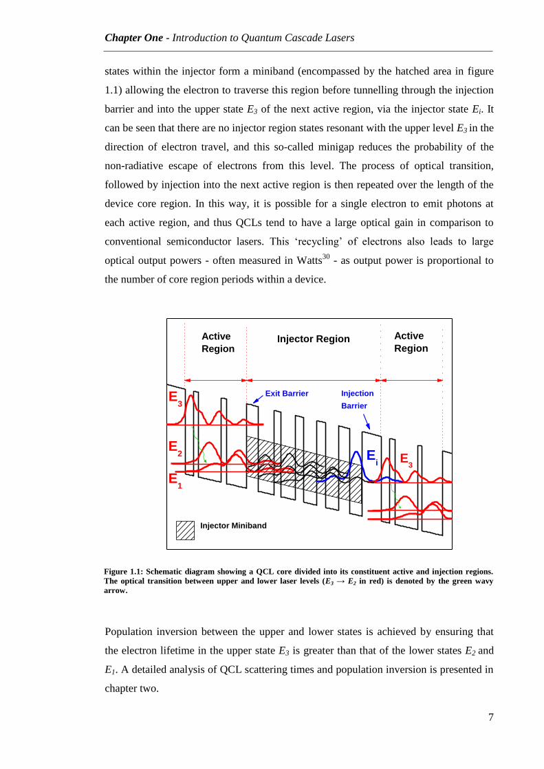
figure 1.1 is part of the biased conduction band offset for the core region of a
GaAs/AlGaAs QCL, encompassing an active region followed by an injection region -
which together constitute one core region period - followed by a second active region. A
complete QCL core region can be comprised of up to around fifty repeats of these
periods.
The active region on the left of the figure is made up of three quantum wells (although
active regions featuring four wells are also common), and the moduli squared of the first
three confined electronic states associated with these wells at energy levels E3, E2 and
E1 are shown in red. Assuming an electron is injected into the upper state E3 from the
preceding injector region, an optical transition can take place between E3 → E2 resulting
in the emission of a photon (represented by the green arrow), where the emission
wavelength is determined by the energy separation of E3 and E2. The electron then
quickly scatters to the lower state E1 where it can tunnel into the injector region. The
Chapter One - Introduction to Quantum Cascade Lasers
7
states within the injector form a miniband (encompassed by the hatched area in figure
1.1) allowing the electron to traverse this region before tunnelling through the injection
barrier and into the upper state E3 of the next active region, via the injector state Ei. It
can be seen that there are no injector region states resonant with the upper level E3 in the
direction of electron travel, and this so-called minigap reduces the probability of the
non-radiative escape of electrons from this level. The process of optical transition,
followed by injection into the next active region is then repeated over the length of the
device core region. In this way, it is possible for a single electron to emit photons at
each active region, and thus QCLs tend to have a large optical gain in comparison to
conventional semiconductor lasers. This ‘recycling’ of electrons also leads to large
optical output powers - often measured in Watts30
- as output power is proportional to
the number of core region periods within a device.
E3
Injection
Barrier
Active
Region
E3
E1
Ei
E2
Active
RegionInjector Region
Injector Miniband
Exit Barrier
Population inversion between the upper and lower states is achieved by ensuring that
the electron lifetime in the upper state E3 is greater than that of the lower states E2 and
E1. A detailed analysis of QCL scattering times and population inversion is presented in
chapter two.
Figure 1.1: Schematic diagram showing a QCL core divided into its constituent active and injection regions.
The optical transition between upper and lower laser levels (E3 → E2 in red) is denoted by the green wavy
arrow.
Chapter One - Introduction to Quantum Cascade Lasers
8
The device emission wavelength can be controlled by adjusting the position of the
electronic states within the active region, primarily through variation in the width of the
quantum wells and barriers. This is in direct contrast to interband lasers in which the
wavelength is determined by the band gap - a property of the material system itself - and
means that for a QCL, a wide range of wavelengths can be achieved for a particular
material. GaAs QCLs for example, have exhibited emission over wavelengths spanning
λ~7µm on the shorter side31
, up to λ>100µm in the case of modern THz devices22
.
1.5 Active Region Design
Three and four-well active regions
The large scope for variation in the sequence of quantum wells and barriers that
constitute the core region of a QCL structure has led to a range of differing active region
designs. Through systematic adjustment to the number and width of the active region
wells and barriers, parameters such as emission wavelength, injection efficiency and
electron scattering rates can all be controlled. One of the most common active region
configurations currently utilised consists of either three or four quantum wells32,33
,
bounded by an injection and exit barrier through which electrons enter and exit the
active region respectively (see figure 1.1). As demonstrated by Faist et al, the
population inversion attainable between the upper and lower laser levels can be
dramatically increased by ensuring the energy spacing between the two (or more) lower
levels is approximately equal to that of an LO phonon in the well material -
ħωLO~36meV for GaAs - which allows the electron scattering lifetime between these
levels to be significantly reduced through resonance with LO phonon emission.
Lifetimes of the order of 0.4ps in the case of three-well designs, and 0.25ps for four-
well active regions have been demonstrated, in comparison to over 1ps for electron
scattering from the upper laser level to lower levels. These short lower level lifetimes
aid rapid depopulation of the lower laser level and increase both the overall population
inversion within the active region, and the optical gain required for lasing.
A further benefit of the three and four-well active regions is the control they allow over
the coupling between the upper laser level and the injector level, which can be enhanced
through adjustment to the width of the thin quantum well adjacent to the injection

Chapter One - Introduction to Quantum Cascade Lasers
9
barrier. This allows electrons to be injected into the active region with increased
efficiency, and reduces the probability of direct non-radiative transitions from the
injector region to the lower laser levels. As well as controlling electron lifetimes at
particular energy levels within the active region, the spatial nature of the optical
transition itself can also be engineered. As will be expanded upon in chapter two, the
active region can be tailored such that upper state electron wavefunction primarily
occupies either the first or second active region quantum well. In the case of the former,
transitions will occur between wells and across the well-barrier interface in a so-called
diagonal transition, whereas in the latter the transition will be vertical, taking place
between confined states within the same quantum well. Whether optical transitions are
diagonal or vertical has consequences for the transition probability, upper laser level
lifetime and ultimately the population inversion within the active region.
Bound-to-continuum and continuum-to-continuum active regions:
The bound-to-continuum (BTC) active region design34
, shown in figure 1.2, aims to
reproduce the good injection efficiency associated with three and four-well active
regions, whilst increasing the efficiency with which electrons are typically extracted
from the lower laser levels into the injector. In the case of the four-well design, the rate
at which electrons resonantly tunnel through the exit barrier from the lowest laser levels
into the injector region is around 10 times slower than the rate of electron scattering
between the lower levels themselves (1ps compared to 0.1ps respectively). This
discrepancy can lead to a reduction in population inversion through the build-up of
electrons in the lower levels29
, particularly at higher temperatures where electrons are
able to repopulate these levels through thermal backfilling. The BTC active region
addresses this issue by replacing the discrete lower levels with a continuum of
electronic states similar to that found within the injector of standard QCL active region
designs.

Chapter One - Introduction to Quantum Cascade Lasers
10
0 10 20 30 40 50 60 70-1.0
-0.5
0.0
0.5
1.0
1.5
Eu E
i
En
erg
y (
eV
)
Distance (nm)
Eu
Ei
Figure 1.2: QCL Γ-point conduction band profile illustrating the bound-to-continuum active region concept.
Optical transitions take place between the upper laser level Eu (shown in red) and a lower continuum of
electronic states (multicoloured), before electrons relax along the injector region and are re-injected into the
next active region via the state Ei (blue).
This arrangement is achieved by incorporating into the core region a superlattice
structure comprising of a series of quantum wells that decrease in width in the direction
of electron travel. Rather than the discrete active and injector regions that comprise the
core of QCLs featuring three and four-well designs, this structure results in a core with
less differentiation between active and injector regions, and a configuration of electronic
states in which optical transitions occur between a single discrete upper state, and a
lower continuum of states. The advantage of this continuum lies in the fact that
electrons scatter through the lower states on a sub-picosecond timescale, avoiding the
potential build-up of electrons that can occur in the lower laser levels of the three and
four-well designs. Injection efficiency is maintained since electrons continue to be
injected from the miniband into the next upper laser level via resonant tunnelling, as is
the case with three and four-well active regions.
A further consequence of the BTC design is the broad gain spectrum that arises from the
optical transitions between the upper laser level and the large number of states within
the lower miniband. This is beneficial for spectroscopic application in which a degree of

Chapter One - Introduction to Quantum Cascade Lasers
11
wavelength tuning of the laser output is required, for example when analysing gases
containing multiple molecule types which would be expected to have several absorption
lines at different wavelengths. The gain spectrum can be further widened by extending
the concept of the bound to continuum active region to a continuum to continuum
design, in which optical transitions are made between an upper and lower continuum,
rather than the discrete upper level as for the BTC design. The increase in the number
and energy range of states from which optical transitions take place can result in a
suitably broadened gain spectrum, with widths of up to 430cm-1
being recently
reported35
.
1.6 Material Systems for QCL Fabrication: Benefits
and Disadvantages of GaAs
To-date, QCL research has primarily focussed on two particular III-V semiconductor
compounds as a basis for the fabrication of device structures; namely indium-phosphide
(InP) and gallium-arsenide (GaAs). Historically, InP-based devices have attracted a far
greater proportion of research, due mainly to the superior device performance that can
be achieved when compared to QCLs based on the GaAs material system. It was a QCL
featuring an InGaAs/AlInAs active region, grown lattice matched to an InP substrate
that first demonstrated lasing in 1994, and since that time the range of materials from
which InP-based QCLs have been fabricated has increased to include systems such as
InGaAs/AlAsSb36
and InGaAs/AlAs37,38
. The first devices developed using the GaAs
material system appeared in 199839
, four years after the emergence of the first InP-based
QCLs. Although Page and co-workers reported achievements such as room temperature
pulsed operation40
, and low-temperature (150K) continuous wave operation41
a
relatively short time after this, subsequent progress has become somewhat sporadic,
with the result being that the CW performance reported by Page et al over a decade ago
has yet to be surpassed. The reasons for the lack of progress in relation to GaAs devices
can mainly be attributed to its intrinsic material properties, and the kind of performance
levels that these properties afford QCLs. For example, the shallow conduction band
offset of ΔEc=0.39eV afforded by GaAs/AlGaAs active regions limits device emission
wavelengths to λ≈8µm and above, while also increasing the probability of electron

Chapter One - Introduction to Quantum Cascade Lasers
12
escape from the upper laser level into the continuum states that exist above the top of
the conduction band. This non-radiative escape channel can act to reduce the population
inversion between upper and lower laser levels and thus restrict device performance.
Also, since the LO phonon-mediated electron scattering lifetime within the QCL active
region is essentially inversely proportional to the electron effective mass (m*)42
, the
comparatively large m*=0.067m0 possessed by GaAs leads to reduced scattering
lifetimes in comparison to InP-based devices (m*=0.043m0 for InGaAs), and thus lower
levels of population inversion and gain. A detailed description of the physics of QCL
active regions, including a comprehensive analysis of electron lifetimes, scattering rates
and population inversion is presented in chapter two.
This seeming inferiority inherent in the material characteristics of GaAs does not
necessarily preclude it as a viable QCL material however, and indeed there are certain
advantages to utilising this material system over the more commonly used InP. GaAs is
one of the most widely studied of all the III-V semiconductor compounds and its
production has been successfully implemented on the industrial scale. This has obvious
economical benefits for any attempt to mass-produce GaAs-based devices. The fact that
AlxGa1-xAs is lattice matched to GaAs for all values of x allows for flexibility in active
region design without the need for strain compensation, while also easing the growth
constraints for the GaAs/AlGaAs active regions since only the Al source needs to be
switched during growth. Nevertheless, the material properties of GaAs can still be
regarded as something of a drawback when compared to InP and its associated material
systems. One strategy for overcoming these limitations is to focus less on fundamental
material properties and more on areas of overall device design in an effort to improve
performance. In this respect, a promising area of investigation involves improvements
to the QCL waveguide used to confine the optical mode within the device active region.
In the case of GaAs-based devices, the waveguide is usually formed using either highly-
doped GaAs or high aluminium content Al0.9Ga0.1As, both of which have drawbacks
associated with their use. In the case of highly-doped GaAs, optical losses can be very
high due to free-carrier absorption, while Al0.9Ga0.1As can exhibit poor electrical
characteristics. A detailed discussion of the disadvantages of conventional GaAs QCL
waveguides is presented in chapter four, while the use of alternative semiconductor
materials as QCL waveguides - in an attempt to overcome the limitations of GaAs and
AlGaAs, and improve device performance - will form a major part of this thesis.

Chapter One - Introduction to Quantum Cascade Lasers
13
1. A. A. Kosterev and F. K. Tittel, Chemical sensors based on quantum cascade lasers, IEEE Journal
of Quantum Electronics, 38, 582-591, (2002).
2. A. Kosterev, G. Wysocki, Y. Bakhirkin, S. So, R. Lewicki, M. Fraser, F. Tittel and R. F. Curl,
Application of quantum cascade lasers to trace gas analysis, Applied Physics B-Lasers and Optics, 90,
165-176, (2008).
3. Pranalytica [Online], Available at: http://www.pranalytica.com/index.php, (2013).
4. Quantum cascade lasers, mid infrared spectroscopy gas analysers from Cascade Technolgies
[Online], Available at: http://www.cascade-technologies.com, (2013).
5. QuantaRed Technologies - Oil in Water Analyzers [Online], Available at: http://quantared.com,
(2013).
6. R. Maulini, A. Lyakh, A. G. Tsekoun, R. Go, M. Lane, T. Macdonald and C. K. N. Patel, High
power, high efficiency quantum cascade laser systems for directional infrared countermeasures and other
defense and security applications, Proceedings of the SPIE, 7483, 74830D, (2009).
7. C. Bauer, A. K. Sharma, U. Willer, J. Burgmeier, B. Braunschweig, W. Schade, S. Blaser, L.
Hvozdara, A. Müller and G. Holl, Potentials and limits of mid-infrared laser spectroscopy for the
detection of explosives, Applied Physics B, 92, 327-333, (2008).
8. J. H. Shorter, D. D. Nelson, J. B. McManus, M. S. Zahniser and D. K. Milton, Multicomponent
Breath Analysis With Infrared Absorption Using Room-Temperature Quantum Cascade Lasers, IEEE
Sensors Journal, 10, 76-84, (2010).
9. R. F. Kazarinov and R. A. Suris, Possibility of amplification of electromagnetic waves in a
semiconductor with a superlattice, Soviet Physics: Semiconductors, 5, 707, (1971).
10. L. C. West and S. J. Eglash, First observation of an extremely large dipole infrared transition
within the conduction band of a GaAs quauntum well, Applied Physics Letters, 46, 1156-1158, (1985).
11. M. Helm, P. England, E. Colas, F. Derosa and S. J. Allen, Intersubband emission from
semiconductor superlattices excited by sequential resonant tunneling, Physical Review Letters, 63, 74-77,
(1989).
12. F. Capasso, K. Mohammed and A. Y. Cho, Sequential resonant tuneling through a multiquantum
well superlattice, Applied Physics Letters, 48, 478-480, (1986).
13. P. F. Yuh and K. L. Wang, Novel infrared band-aligned superlattice laser, Applied Physics
Letters, 51, 1404-1406, (1987).
14. H. C. Liu, A novel superlattice infrared source, Journal of Applied Physics, 63, 2856-2858,
(1988).

Chapter One - Introduction to Quantum Cascade Lasers
14
15. J. Faist, F. Capasso, D. L. Sivco, C. Sirtori, A. L. Hutchinson and A. Y. Cho, Quantum Cascade
Laser, Science, 264, 553-556, (1994).
16. C. Gmachl, F. Capasso, D. L. Sivco and A. Y. Cho, Recent progress in quantum cascade lasers
and applications, Reports on Progress in Physics, 64, 1533-1601, (2001).
17. J. Faist, F. Capasso, C. Sirtori, D. L. Sivco, A. L. Hutchinson and A. Y. Cho, Continuous-wave
operation of a vertical transition quantum cascade laser above T=80K, Applied Physics Letters, 67,
3057-3059, (1995).
18. J. Faist, F. Capasso, C. Sirtori, D. L. Sivco, A. L. Hutchinson and A. Y. Cho, Room temperature
mid-infrared quantum cascade lasers, Electronics Letters, 32, 560-561, (1996).
19. J. Faist, F. Capasso, C. Sirtori, D. L. Sivco, J. N. Baillargeon, A. L. Hutchinson, S. N. G. Chu and
A. Y. Cho, High power mid-infrared (l~5mm) quantum cascade lasers operating above room
temperature, Applied Physics Letters, 68, 3680-3682, (1996).
20. M. Beck, D. Hofstetter, T. Aellen, J. Faist, U. Oesterle, M. Ilegems, E. Gini and H. Melchior,
Continuous wave operation of a mid-infrared semiconductor laser at room temperature, Science, 295,
301-305, (2002).
21. O. Cathabard, R. Teissier, J. Devenson, J. C. Moreno and A. N. Baranov, Quantum cascade lasers
emitting near 2.6mm, Applied Physics Letters, 96, 141110, (2010).
22. B. S. Williams, Terahertz quantum-cascade lasers, Nature Photonics, 1, 517-525, (2007).
23. Y. Bai, N. Bandyopadhyay, S. Tsao, E. Selcuk, S. Slivken and M. Razeghi, Highly temperature
insensitive quantum cascade lasers, Applied Physics Letters, 97, 251104, (2010).
24. N. Bandyopadhyay, Y. Bai, B. Gokden, A. Myzaferi, S. Tsao, S. Slivken and M. Razeghi, Watt
level performance of quantum cascade lasers in room temperature continuous wave operation at λ~3.76
μm, Applied Physics Letters, 97, 131117, (2010).
25. Y. Bai, N. Bandyopadhyay, S. Tsao, S. Slivken and M. Razeghi, Room temperature quantum
cascade lasers with 27% wall plug efficiency, Applied Physics Letters, 98, 181102, (2011).
26. A. Hugi, R. Terazzi, Y. Bonetti, A. Wittmann, M. Fischer, M. Beck, J. Faist and E. Gini, External
cavity quantum cascade laser tunable from 7.6 to 11.4mm, Applied Physics Letters, 95, 061103, (2009).
27. N. Owschimikow, C. Gmachl, A. Belyanin, V. Kocharovsky, D. L. Sivco, R. Colombelli, F.
Capasso and A. Y. Cho, Resonant second-order nonlinear optical processes in quantum cascade lasers,
Physical Review Letters, 90, 043902, (2003).
28. C. Gmachl, A. Belyanin, D. L. Sivco, M. L. Peabody, N. Owschimikow, A. M. Sergent, F.
Capasso and A. Y. Cho, Optimized second-harmonic generation in quantum cascade lasers, IEEE Journal
of Quantum Electronics, 39, 1345-1355, (2003).
Chapter One - Introduction to Quantum Cascade Lasers
15
29. J. Cockburn, Mid-infrared quantum cascade lasers, Mid-Infrared Semiconductor Optoelectronics,
323-355, (Springer, 2006).
30. M. Razeghi, High-Performance InP-Based Mid-IR Quantum Cascade Lasers, IEEE Journal of
Selected Topics in Quantum Electronics, 15, 941-951, (2009).
31. L. R. Wilson, J. W. Cockburn, M. J. Steer, D. A. Carder, M. S. Skolnick, M. Hopkinson and G.
Hill, Decreasing the emission wavelength of GaAs-AlGaAs quantum cascade lasers by the incorporation
of ultrathin InGaAs layers, Applied Physics Letters, 78, 413-415, (2001).
32. C. Sirtori, J. Faist, F. Capasso, D. L. Sivco, A. L. Hutchinson, S. N. G. Chu and A. Y. Cho,
Continuous wave operation of midinfrared (7.4-8.6mm) quantum cascade lasers up to 110 K temperature,
Applied Physics Letters, 68, 1745-1747, (1996).
33. D. Hofstetter, M. Beck, T. Aellen and J. Faist, High-temperature operation of distributed feedback
quantum-cascade lasers at 5.3μm, Applied Physics Letters, 78, 396-398, (2001).
34. J. Faist, M. Beck, T. Aellen and E. Gini, Quantum-cascade lasers based on a bound-to-continuum
transition, Applied Physics Letters, 78, 147-149, (2001).
35. Y. Yao, X. J. Wang, J. Y. Fan and C. F. Gmachl, High performance "continuum-to-continuum"
quantum cascade lasers with a broad gain bandwidth of over 400 cm-1
, Applied Physics Letters, 97,
081115, (2010).
36. D. G. Revin, L. R. Wilson, E. A. Zibik, R. P. Green, J. W. Cockburn, M. J. Steer, R. J. Airey and
M. Hopkinson, InGaAs/AlAsSb quantum cascade lasers, Applied Physics Letters, 85, 3992-3994, (2004).
37. K. Ohtani and H. Ohno, An InAs-based intersubband quantum cascade laser, Japanese Journal of
Applied Physics Part 2-Letters, 41, L1279-L1280, (2002).
38. M. P. Semtsiv, M. Ziegler, S. Dressler, W. T. Masselink, N. Georgiev, T. Dekorsy and M. Helm,
Above room temperature operation of short wavelength (l=3.8mm) strain-compensated In0.73Ga0.27As-
AlAs quantum-cascade lasers, Applied Physics Letters, 85, 1478-1480, (2004).
39. C. Sirtori, P. Kruck, S. Barbieri, P. Collot, J. Nagle, M. Beck, J. Faist and U. Oesterle,
GaAs/AlxGa1-xAs quantum cascade lasers, Applied Physics Letters, 73, 3486-3488, (1998).
40. H. Page, C. Becker, A. Robertson, G. Glastre, V. Ortiz and C. Sirtori, 300 K operation of a GaAs-
based quantum-cascade laser at l ~ 9mm, Applied Physics Letters, 78, 3529-3531, (2001).
41. H. Page, S. Dhillon, M. Calligaro, C. Becker, V. Ortiz and C. Sirtori, Improved CW operation of
GaAs-Based QC lasers: T-max=150 K, IEEE Journal of Quantum Electronics, 40, 665-672, (2004).
42. J. Faist, F. Capasso, C. Sirtori, D. L. Sivco and A. Y. Cho, Quantum Cascade Lasers,
Intersubband Transitions in Quantum Wells: Physics and Device Applications II, (Academic Press, 1999).
16
Chapter Two
Quantum Cascade Lasers:
Theory and Principles of
Operation
2.1 Introduction
The following sections present an overview of some of the basic theoretical concepts
that are fundamental to the operation of the quantum cascade laser. As well as a
mathematical treatment, the properties that can be derived from these concepts will be
examined in relation to their effect on laser design. Firstly, the nature of photon
generation within the laser active region will be discussed, in the context of the quantum
mechanics of intersubband transitions - in particular the spontaneous transition of
electrons between subbands. The intersubband gain will then be reviewed. By
considering a simplified model of electronic transitions based upon a three-level system
within the active region, rate equations will be used to derive several operating
parameters of the QCL such as the population inversion between electron energy levels
and the laser threshold current density. The chapter ends with a discussion of the
methods used to model the confinement of the optical mode within the laser active
region, necessary when evaluating the effectiveness of a particular waveguide design to
be used within the laser structure.

Chapter Two - Quantum Cascade Lasers: Theory and Principles of Operation
17
2.2 Intersubband Transitions
The analysis of electronic transitions between the subbands of a semiconductor
heterostructure begins by applying Fermi’s golden rule, which describes the electron
transition rate Wif, from an initial state i, to a final state f due to perturbation from an
external electromagnetic field1:
|⟨ |
| ⟩| ( )
(2.1)
where ψi and ψf represent the initial and final electronic wavefunctions respectively, H'
is the interaction Hamiltonian and δ(Ef - Ei - ω) is the density of final states of the
system. In the case of the external field being a linearly polarized plane wave, and
provided its wavelength is greater than the scale over which electrons traverse the QCL
active region, it can be shown that the transition rate is proportional to the square of the
transition dipole matrix element, zij=⟨ | | ⟩1:
|⟨ | | ⟩|
( )
(2.2)
where e is the polarisation vector of the electric field, p is the linear momentum
operator, e the electronic charge, m* the electron effective mass, E0 the amplitude of the
electric field, and ω the angular frequency of the EM radiation. The dipole matrix
element can be tailored during the design of the active region by specifying the quantum
wells in which the electronic wavefunctions associated with the laser transition have
their maximum probability densities. Transitions that occur between states within the
same quantum well (vertical transitions) have larger dipole moments that those that
occur between adjacent wells (diagonal transitions), are therefore more probable and
have a correspondingly higher transition rate.

Chapter Two - Quantum Cascade Lasers: Theory and Principles of Operation
18
Within the QCL active region there are several mechanisms by which an electron
occupying the upper laser level can undergo a transition to a lower energy level,
including non-radiative processes such as phonon and electron-electron scattering. It is
the spontaneous radiative transition of electrons between subbands however, and the
resultant emission of photons that provide the basis for further stimulated emission, gain
and ultimately lasing. It can be shown that following on from equation 2.1, the
spontaneous emission rate of photons Wi fsp
, is given by2:
(2.3)
where zij is the transition dipole matrix element, nref is the refractive index of the laser
medium, c is the speed of light in a vacuum, ε0 is the permittivity of free space and Eij
the energy of the transition; i.e. Ei-Ej. As well as demonstrating the same quadratic
dependence on dipole matrix element seen in equation 2.2, it can be seen that the
spontaneous radiative transition rate is also related to the emission wavelength,
manifested in the energy term Eij. This wavelength dependence is also quadratic if the
transition rate is expressed as a product of the transition energy and the transition
oscillator strength, and results in increasing transition lifetimes at longer wavelengths.
For QCLs emitting in the mid-infrared, these lifetimes can be several orders of
magnitude longer than some non-radiative processes such as LO phonon scattering
which occur on a picosecond time scale3, and lead to the low spontaneous radiative
efficiencies observed for QCLs.
2.3 Intersubband Gain
As with any type of laser, the amount by which optical emission can be amplified within
the laser medium - the gain - is a key indicator of QCL performance. The previous
section detailed the emission of photons due to the spontaneous transition of electrons
between two subbands of the conduction band. In order to achieve lasing however, it is
necessary for these spontaneously emitted photons to themselves interact with electrons

Chapter Two - Quantum Cascade Lasers: Theory and Principles of Operation
19
in the upper laser level, triggering further electronic transitions to the lower level. The
subsequent stimulated emission of photons that occurs as a result of these interactions
leads to an increase in the photon density within the laser medium, and thus optical
gain. For a QCL, the peak material gain Gp, that can be achieved between two subbands
i and j is given by4:
( )
(2.4)
where nref is the refractive index associated with the laser mode, λ the emission
wavelength, 2γij the spontaneous emission full width at half-maximum, determined from
electroluminescence measurements and nj-ni is the difference in electron sheet densities
between subbands i and j. The term Lp contained in the denominator is a normalisation
factor - normally taken to be the length of a single active region period. The terms on
the right-hand side of equation 2.4 are commonly collected together and termed the gain
cross-section, gc - i.e. the peak modal gain per unit of upper state population:
(2.5)
where Γ is the confinement factor of the optical mode, i.e. the fraction of the optical
mode that is confined within the active region section of the complete QCL structure.
The dependence of the gain on electronic population inversion will be expanded upon
within the discussion of QCL rate equations in section 2.4. In terms of the relationship
between the gain and the transition dipole matrix element zij, equation 2.4 shows that
once more a quadratic dependence is predicted. It has been discussed above how it is
possible to tailor the dipole matrix through the confinement of the electron
wavefunctions within specific quantum wells of the active region; however, the
dependence of gain on the optical dipole also influences the choice of material system to
be used for device fabrication.

Chapter Two - Quantum Cascade Lasers: Theory and Principles of Operation
20
The energies of the quantised levels within a quantum well are inversely proportional to
both the particle mass (or effective mass m*, in the case of electrons in a
semiconductor), and the square of the well width. Since the effective electron mass for
GaAs is m*=0.067m0 - larger than, for example, InGaAs (m*=0.043m0) - for an
equivalent energy separation GaAs-based QCLs require narrower quantum wells in the
active region than their InP-based counterparts. The reduction in well width however,
brings with it a concomitant decrease in dipole matrix element and gain, and as such
represents one of the fundamental disadvantages of the GaAs/AlGaAs material system
compared to InGaAs/AlInAs/InP.
2.4 QCL Rate Equations
Several important parameters that characterise the operation of a QCL can be derived
through an analysis of a simplified, sub-threshold three-level active region, and the
electronic transitions associated with it. By considering the rates at which these
transitions occur, it is possible to determine the conditions for population inversion -
essential for the operation of any laser - as well as an expression for the threshold
current density. Shown in figure 2.1 is a schematic representation of a sub-threshold
three-level active region, and the various current paths and electronic transitions
possible within. From the perspective of maximising the population inversion between
the upper and lower energy levels (E3 and E2 respectively), it is obviously desirable that
the current injected into the active region from the preceding injector level - shown as
the current density J3 for dimensional consistency - populates E3 with 100% efficiency.
There is however the possibility of a parasitic current path J2, from the injector level
directly to E2 which will act to reduce the population inversion.
Once electrons have been injected into the active region several possible transitions can
then occur, each with an associated transition rate τ-1
, where τ is the lifetime for which
an electron will remain at a particular energy level. For electrons that have been injected
directly into level E3, a transition can occur between E3 and E2 (which would be an
optical transition above threshold) at a rate τ32-1
. This can then be followed by a
transition from E2 to E1 at a rate τ21-1
, before electrons exit the active region via resonant
tunnelling from E1 to the adjacent injector level, again with associated rate τ1i-1
. In

Chapter Two - Quantum Cascade Lasers: Theory and Principles of Operation
21
addition to this pathway, there also exist several other non-radiative transitions available
to electrons which reduce the overall efficiency of the active region. For electrons
occupying level E3, rather than making the transition E3 → E2, it is possible to transition
directly to the lowest energy level E1 (at rate τ31-1
), or to escape directly into the
continuum states above the injector miniband (at rate τesc-1
). For those electrons that
have made the transition from E3 → E2, escape directly from E2 is also possible -
signified by τ2i-1
.
Figure 2.1: Schematic diagram illustrating a simplified three-level QCL active region, and the various electron
pathways that exist within. This scheme forms the basis from which the rate equations presented in section
2.4.1 are derived.
2.4.1 Population Inversion
Derivation of the conditions for population inversion begins with a consideration of the
relative sub-threshold electron sheet densities n3 and n2 (in cm-2
) of levels E3 and E2
respectively, and the rate at which electrons depopulate these levels via the mechanisms
described above. With reference to figure 2.1 it can be seen that the rate of change
dn/dt, of the population n3 is given by the expression:
(2.6)

Chapter Two - Quantum Cascade Lasers: Theory and Principles of Operation
22
and similarly for n2:
(2.7)
with all terms as previously defined. Below threshold it is assumed that the system is in
the steady state, i.e:
(2.8)
By setting equations 2.6 and 2.7 equal to zero it can be shown that:
(
)
(2.9)
and
(
)
(
)
(2.10)
By substituting equation 2.9 into equation 2.10 and assuming that the current that is
injected into E3 is very much greater than E2 (i.e. that J2/J3 → 0) we arrive at:
(
)
(2.11)

Chapter Two - Quantum Cascade Lasers: Theory and Principles of Operation
23
The electron lifetimes τ21 and τ2i (representing transitions from E2 → E1 and from E2 to
the injector respectively) can be combined into a single lifetime τ2, representing the total
time for which electrons populate E2.
We therefore now have the condition that the ratio of the electron populations n3 and n2
is directly proportional to the ratio of the lifetimes between the transition E3 → E2 and
that of level E2, i.e:
(2.12)
Thus, as one would expect, in order to achieve a population inversion (i.e. n3/n2 > 1) we
require that the transition lifetime τ32 is greater than the lifetime τ2 for which electrons
occupy level E2.
The population difference Δn=n3-n2, between level E3 and E2 can be calculated by
following a similar exercise to that shown above. Starting with equations 2.6 and 2.7
and the steady state condition that dn/dt=0, and assuming that both the rate of electron
escape from E3 directly into the continuum and the current injected directly into E2 are
very small (i.e. 1/τesc and J2 ≈ 0), we arrive at expressions for the populations n3 and n2:
and (
) (2.13a and 2.13b)
The population difference n3-n2 can be expressed using equation 2.13b:
(
) (2.14)

Chapter Two - Quantum Cascade Lasers: Theory and Principles of Operation
24
Combining equations 2.13a and 2.13b leads to:
(2.15)
which when combined with equation 2.14 results in a final expression for Δn:
(
)
(2.16)
In the same way that achieving population inversion requires a longer upper state
lifetime in relation to the E2 lifetime, it is seen that in order to subsequently maximise
the difference between upper and lower level populations, the difference between these
lifetimes must also be maximised. As is indicated by equation 2.4, any increase in the
ratio τ32/τ2 will also have the corresponding effect of increasing the QCL gain, which is
directly proportional to the population difference between E3 and E2. Increasing the
upper state lifetime can be achieved in a similar manner to that previously described for
the dipole matrix element, namely by tailoring the spatial position of the electronic
wavefunctions to make transitions more or less probable.
It is generally found however that a reduction of the wavefunction overlap designed to
increase the upper state lifetime, is accompanied by a reduction in the transition dipole
matrix element on which QCL gain is also dependent. Thus a balance must be struck
between these two factors when considering the amount of gain that may be achievable
for any particular QCL design.
2.4.2 Threshold Current Density
A slightly modified set of arguments to those presented above may be used to derive an
expression for the QCL threshold current density Jth. In this instance, a term describing
the rate at which electrons re-occupy E2 through thermal backfilling, n2therm
is added to

Chapter Two - Quantum Cascade Lasers: Theory and Principles of Operation
25
the previous rate equation 2.7, while the electrons injected into the active region are
assumed to occupy E3 with 100% efficiency (i.e. J2=0) giving:
(2.17)
and
( )
(2.18)
where τ3-1
and τ2-1
represent the total scattering rates from E3 and E2 respectively. By
again considering the steady state conditions below threshold (dn3/dt=dn2/dt=0), we
arrive at:
and
(2.19a and 2.19b)
which can be combined to give the population difference Δn=n3-n2 between E3 and E2:
(2.20)
where the total electron effective lifetime τeff is defined as τeff =τ3(1-τ2/τ32). Threshold
current density is reached when the modal gain equals the total loss from the laser
cavity i.e.:
(2.21)

Chapter Two - Quantum Cascade Lasers: Theory and Principles of Operation
26
Substituting for Gp from equations 2.4 and 2.5 leads to:
(2.22)
from which we arrive at:
(
)
(2.23)
Finally, rearranging for J gives the expression for the threshold current density:
⁄
(2.24)
The importance of a large upper state lifetime in comparison to the lifetimes of the
lower laser levels is again apparent from equation 2.24, since for τ32≫τ2, τeff → τ3
leading to lower threshold currents for larger τ32/τ2 ratios (and correspondingly larger
population inversions). In addition to this, it is seen that the losses within the device
must also be minimised in order to achieve smaller threshold currents. Since the total
losses αtot can be separated into those relating to the mirrors at each end of the laser
cavity αm, and the waveguide losses αw (i.e. αtot=αm+ αw), it therefore follows that any
reduction in waveguide loss that can be achieved should result in a lowering of the
device threshold current density. Attempts to reduce αw through the use of material
systems not previously considered for incorporation in QCL waveguides will be one
focus of the experimental chapters of this thesis.
2.4.3 Slope Efficiency
In order to derive the QCL slope efficiency dP/dI, the above-threshold dynamics of the
active region must be considered, whereby the gain becomes fixed and the photon flux
S, within the active region increases linearly with current density2. Modified forms of

Chapter Two - Quantum Cascade Lasers: Theory and Principles of Operation
27
the QCL rate equations, which now include a term for the photon flux S, per period, per
unit active region width are given by:
(2.25)
and
(2.26)
An expression for the rate of change of S with current density can obtained by
considering the situation at threshold where the optical gain becomes fixed, and is equal
to the total optical loss i.e. gc∆n=αtot. By setting the derivatives in equations 2.25 and
2.26 to zero and substituting for gc∆n, we arrive, at some length, at an expression for
dS/dJ:
( )
(2.27)
where αtot is the total loss from the laser cavity and τeff is as previously defined in
equation 2.20. The slope efficiency is then found using the derivative of the photon flux:
(2.28)
where Np is the number of core region periods within the QCL structure and αm the
cavity mirror loss.

Chapter Two - Quantum Cascade Lasers: Theory and Principles of Operation
28
The slope efficiency can therefore be expressed as:
(2.29)
2.5 QCL Waveguides
In order to maximise the rate of stimulated emission of photons within the laser core,
and to prevent unwanted losses to the QCL layers that surround it, a method of
confining the optical mode within the QCL active region is needed. The most common
approach is to form a dielectric slab waveguide by surrounding the core with two layers
of semiconductor material that both posses a smaller refractive index than that of the
active region. The refractive index contrast acts to limit the optical mode penetration
from core to outer layers in the growth direction, while lateral confinement is provided
by the walls of the ridge structure itself.
The confinement of the optical mode within the QCL structure can be modelled once
various parameters relating to the materials to be used in the structure are known. It is
generally necessary to first calculate the real and imaginary parts of the complex
dielectric constant for each material layer. These two parameters - ε1 and ε2 respectively
- are given by5:
(2.30)
and
(2.31)

Chapter Two - Quantum Cascade Lasers: Theory and Principles of Operation
29
where ε∞ is the high-frequency dielectric constant, e is the electronic charge, N is the
doping concentration per unit volume, ε0 the permittivity of free space, m* the electron
effective mass, ω the angular frequency of emitted radiation and τ the electron
scattering time. The quantities ε∞, ε0, m* and τ for each material can be found in the
relevant literature, allowing ε1 and ε2 to be calculated and subsequently used to
determine the real and imaginary parts of the refractive index (n and k respectively) for
each layer6:
[
]
(2.32)
and
[
]
(2.33)
Equations 2.30 through 2.33 enable the complex refractive index to be modelled as a
function of doping concentration N, and thus N can be chosen such that it results in a
desired value of n and k for each layer of the QCL structure. Once the parameters n, k
and ε0 are known for each layer, the optical mode profile for the complete structure can
be simulated using specialist software. Since the dipole transitions that result in QCL
emission take place in the plane of the direction of growth (conventionally taken as the
z-direction), emission is in the x-y plane - i.e. edge-emitting - and is transverse-
magnetic (TM) polarised. Optical mode profiles are therefore calculated for the TM
rather than transverse electric (TE) mode. Of particular relevance to waveguide design
is the mode confinement factor Γ, defined previously in equation 2.5, which can be
calculated by integrating the profile over each separate layer (see appendix A.2). The
waveguide losses αw, can also be calculated in a similar manner. Several examples of
optical mode profiles determined using this method are presented in chapter four, in
figures 4.1 through 4.4.

Chapter Two - Quantum Cascade Lasers: Theory and Principles of Operation
30
1. M. Helm, The Basic Physics of Intersubband Transitions, Intersubband Transitions in Quantum
Wells: Physics and Device Applications I, (Academic Press, 1999).
2. J. Faist, Quantum Cascade Lasers, (OUP, 2013).
3. R. Ferreira and G. Bastard, Evaluation of some scattering times for electrons in unbiased and
biased single- and multiple-quantum-well structures, Physical Review B, 40, 1074-1086, (1989).
4. J. Faist, F. Capasso, C. Sirtori, D. L. Sivco and A. Y. Cho, Quantum Cascade Lasers,
Intersubband Transitions in Quantum Wells: Physics and Device Applications II, (Academic Press, 1999).
5. F. Capasso, A. Y. Cho, J. Faist, A. L. Hutchinson, C. Sirtori and D. L. Sivco, Article Comprising a
Semiconductor Waveguide Structure, United States Patent 5502787, (1996).
6. A. M. Fox, Optical Properties of Solids, (OUP, 2001).

31
Chapter Three
Semiconductor Growth and Device
Fabrication and Characterisation
3.1 Introduction
The transformation of a wafer of semiconductor material into a working QCL device,
and the testing and measurement required to determine its optical and electrical
characteristics involves numerous processes, many of which must be carried out in
highly regulated clean-room environments. The chapter begins with a discussion of the
epitaxy used to grow the semiconductor wafer structure from which lasers are
subsequently fabricated, before describing details of the growth as it relates specifically
to the GaAs-based wafers used in this work. The various lithographic, etching and
bonding processes involved in the fabrication of the devices featured in the
experimental chapters of this thesis are then considered, before ending with a
presentation of the techniques employed to characterise devices such as Fourier
Transform Infra-red Spectroscopy, current-voltage and current-power measurements,
and determination of waveguide losses and characteristic temperature.

Chapter Three - Semiconductor Growth and Device Fabrication and Characterisation
32
3.2 Metal-Organic Vapour Phase Epitaxy
Due to the nature of the QCL structure, a growth technique is required that on the one
hand allows precise control of the nanometre-scale repeating layers of the active region,
whilst on the other allows the rapid growth of the surrounding micron-thick cladding
layers. The ability to grow a wide range of semiconductor materials to accommodate
differing QCL designs is also required. In this respect, metal-organic vapour phase
epitaxy (MOVPE) is an ideal choice for QCL growth, and all wafers presented in this
thesis were grown using MOVPE at the National Centre for III-V Technologies in
Sheffield1.
In contrast to methods such as molecular beam epitaxy (MBE) which use solid sources
as the basis for material deposition, MOVPE utilises gasses flowing over a heated
substrate and the subsequent reactions that occur at the substrate surface to build up
layers of semiconductor. In the general case of III-V semiconductors, metalorganic
compounds of the group III elements are combined with hydrides of group V to produce
the desired alloy2:
(3.1)
The particular gasses used are dependent on the material being grown; for example in
the case of GaAs, a combination of trimethylgallium (Ga(CH3)3) and arsine (AsH3) can
be used to form GaAs plus various organic waste compounds. These so-called precursor
gasses are transported via a carrier gas, usually hydrogen (H2), into the main reaction
chamber which can be held at a pressure between 150 and 750 Torr (atmospheric
pressure). The precursor gasses diffuse toward the heated (typically between 500-
800°C) substrate, whereby they decompose into their constituent components and the
III-V atoms are adsorbed onto its surface at an appropriate point on the crystal lattice.
The organic molecules are desorbed from the surface and diffuse away from the
substrate before being carried out of the chamber as waste gasses3. Gasses can be
switched during growth to allow the formation of different materials and thus the
complete QCL wafer can be grown sequentially.

Chapter Three - Semiconductor Growth and Device Fabrication and Characterisation
33
QCL growth by MOVPE offers a number of advantages over MBE. As already touched
upon, growth rates of up to 5µm/hr are achievable compared to around 0.5µm/hr for
MBE, making MOVPE particularly suitable for growth of the thick semiconductor
layers that surround the QCL active region. The fact that an ultra-high vacuum is not
required during growth also leads to less machine downtime in between growth runs
and during maintenance. These factors combine to make MOVPE a more financially
economical technique in comparison to MBE, especially when producing wafers on an
industrial scale. One further benefit of MOVPE is its ability to grow materials from the
phosphide group - for example InP - using the precursor gas phosphine (PH3). Growth
of phosphides using MBE is more problematic due to the unstable and potentially
dangerous nature of solid-source phosphorus.
For the production of the QCL wafers presented in this work, a horizontal flow,
low-pressure (150 Torr) MOVPE system was used, with growth taking place at 690°C
to produce a series of 2” wafers in each growth run.
3.3 Device Fabrication
Due to the smaller, non-industrial scale of device production within the laboratory
environment it is unusual to work with a complete 2” wafer in a single processing run.
Wafers are therefore hand-cleaved at right-angles to the major and minor-flat (ensuring
breaks are straight and clean), into smaller sections - generally between 1/4 and 1/8 of
the original wafer area - before processing commences. The cleaved wafer section must
then be cleaned to ensure that, along with any other particulate contaminants, no
material fragments that may have been produced as a result of the cleaving process are
present on the wafer surface. A three-stage clean using the solvents n-butyl acetate,
acetone and isopropyl alcohol is used for this purpose. Despite processing taking place
in ISO 6 and ISO 5 category clean rooms (which allow for no more than 8320 and 832
particles greater than 1µm in size per cubic metre respectively4), contaminants remain
present during most stages of fabrication and so this cleaning process is repeated several
times over the course of a processing run in order to maximise final device yield.

Chapter Three - Semiconductor Growth and Device Fabrication and Characterisation
34
Figure 3.1 below shows the main processing steps involved in the fabrication of QCL
devices once the wafer has been sufficiently cleaned. Firstly, a 500nm layer of silicon
dioxide (SiO2) is deposited over the surface of the wafer using plasma-enhanced
chemical vapour deposition (PECVD), which forms the basis of the hard mask used to
define the laser ridges during the subsequent dry-etching of the wafer. To this dielectric
layer is added ~1µm of photoresist (SPR350 positive resist) deposited by spin-coating,
which allows the transfer of the laser ridge pattern to the hard mask. The wafer is then
placed in a mask-aligner (Karl Suss UV300) and positioned underneath a chrome-plated
quartz mask patterned with the ridge structure. Due to the 10° miscut of the wafer
substrate, the sample must be aligned such that the edges formed by the major-flat
cleave are parallel to the laser ridges defined on the mask. This ensures that once
cleaved, the laser facets are both vertical with respect to the top and bottom of the laser,
and perpendicular to the side walls of the laser ridge. The sample is illuminated by ultra-
violet light for approximately 10s, whereby areas of photoresist not shadowed by the
chrome of the mask are exposed to the radiation and those that lie directly underneath
the chrome remain unexposed.
Figure 3.1: Key processing steps for the fabrication of QCL devices. (a) Hard mask and resist deposition. (b)
Ridge photolithography. (c) Hard mask ICP etch. (d) Resist removal. (e) Semiconductor ICP etch. (f) Hard
mask removal. (g) Dielectric deposition. (h) Contact window etch. (i) Gold contact deposition.

Chapter Three - Semiconductor Growth and Device Fabrication and Characterisation
35
Following exposure, samples are immersed in a chemical developer (Microposit
MF26A). UV exposure causes the formation of an acidic compound within the resist
which renders it soluble in the alkaline developer, and thus exposed photoresist is
dissolved and removed from the sample while unexposed resist remains on the sample
surface5. In this way, the laser ridge pattern defined by the mask is imprinted in the
photoresist forming a three-dimensional series of resist stripes. This pattern is then
transferred to the SiO2 layer underneath by inductively-coupled plasma (ICP) etching.
In order to ensure that the resist layer is not removed before the SiO2 etch is completed,
the gasses used during the process must preferentially etch the SiO2 at a faster rate than
the resist. A combination of argon (Ar) and trifluoromethane (CHF3) is used to etch
through the areas of SiO2 not covered by resist, down to the underlying semiconductor
surface. Upon completion of the SiO2 etch, a specialised solvent (Microposit 1165) is
used to remove the remaining photoresist, followed by a secondary three-solvent clean,
to leave the wafer covered only by the SiO2 hard mask which is a copy of the original
resist pattern.
In order to form laser ridges in the semiconductor itself, a second ICP etch is performed
which selectively etches the semiconductor material over the SiO2 of the hard mask.
Different combinations of gasses can be used depending upon the particular material
being etched. In the case of the GaAs-based wafers presented in the experimental
section of this thesis, a mixture of silicon tetrachloride (SiCl4) and argon were used for
devices containing InGaP waveguides, while a two-stage process utilising SiCl4 to etch
the top GaAs layer followed by SiCl4/Ar for the remaining structure was used for
InAlP-containing wafers. In order to monitor the etch depth and ensure that the sample
is not under or over-etched, the intensity of reflected light from λ=960nm laser incident
on the sample surface is measured in-situ during the process and compared to a
calculated model. After etching to the desired depth - usually just below the active
region layer - the remaining SiO2 is removed with the same CHF3/Ar etch used in the
formation of the hard mask to leave a sample that comprises of a series of parallel
semiconductor ridges. These ridges then form the basis for the final QCL devices (see
figure 3.2).

Chapter Three - Semiconductor Growth and Device Fabrication and Characterisation
36
Figure 3.2: Scanning electron microscope image of an ICP etched QCL ridge. The GaAs/AlGaAs active region
can be seen as the lighter coloured band in between the darker InGaP waveguide layers either side.
Electrical isolation of the semiconductor ridges is provided by a 500nm thick layer of
insulating silicon nitride (Si3N4) deposited over the entire wafer by PECVD. Contact
windows are then formed along the entire length of the laser ridges by etching through
the central section of Si3N4 covering the top of the ridges to the semiconductor below, in
order to provide a channel for electrical current once the metallic contacts have been
added. The process of creating the contact windows follows the same lithography and
ICP etch procedure as for the formation of the laser ridges described above, with the
exception that alignment of the sample to the mask pattern is now achieved using
micron-scale alignment keys on both wafer and mask. This ensures that the contact
windows do not drift toward the edge of the ridges as they follow their length, which
can result in the removal of insulator from the side walls of the laser ridges during the
etch, in turn producing short-circuits during device operation. Once etching of the
contact windows is complete, the wafer is stripped of any remaining photoresist and
again three-solvent cleaned.
In preparation for the deposition of the top electrical contact, a further lithographic step
is performed in order to add a series of thin photoresist channels in between each laser
ridge. The sample is then placed inside a thermal evaporator and 10nm of titanium (Ti)
followed by 200nm of gold (Au) are deposited on the top surface - the Ti acting as an
adhesive layer for the Au. The resist channels act to partially shadow the gold as it is
being evaporated, resulting in only partial coverage over these areas. After Au
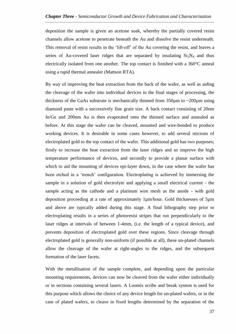
Chapter Three - Semiconductor Growth and Device Fabrication and Characterisation
37
deposition the sample is given an acetone soak, whereby the partially covered resist
channels allow acetone to penetrate beneath the Au and dissolve the resist underneath.
This removal of resist results in the ‘lift-off’ of the Au covering the resist, and leaves a
series of Au-covered laser ridges that are separated by insulating Si3N4 and thus
electrically isolated from one another. The top contact is finished with a 360°C anneal
using a rapid thermal annealer (Mattson RTA).
By way of improving the heat extraction from the back of the wafer, as well as aiding
the cleavage of the wafer into individual devices in the final stages of processing, the
thickness of the GaAs substrate is mechanically thinned from 350µm to ~200µm using
diamond paste with a successively fine grain size. A back contact consisting of 20nm
In/Ge and 200nm Au is then evaporated onto the thinned surface and annealed as
before. At this stage the wafer can be cleaved, mounted and wire-bonded to produce
working devices. It is desirable in some cases however, to add several microns of
electroplated gold to the top contact of the wafer. This additional gold has two purposes;
firstly to increase the heat extraction from the laser ridges and so improve the high
temperature performance of devices, and secondly to provide a planar surface with
which to aid the mounting of devices epi-layer down, in the case where the wafer has
been etched in a ‘trench’ configuration. Electroplating is achieved by immersing the
sample in a solution of gold electrolyte and applying a small electrical current - the
sample acting as the cathode and a platinum wire mesh as the anode - with gold
deposition proceeding at a rate of approximately 1µm/hour. Gold thicknesses of 5µm
and above are typically added during this stage. A final lithography step prior to
electroplating results in a series of photoresist stripes that run perpendicularly to the
laser ridges at intervals of between 1-4mm, (i.e. the length of a typical device), and
prevents deposition of electroplated gold over these regions. Since cleavage through
electroplated gold is generally non-uniform (if possible at all), these un-plated channels
allow the cleavage of the wafer at right-angles to the ridges, and the subsequent
formation of the laser facets.
With the metallisation of the sample complete, and depending upon the particular
mounting requirements, devices can now be cleaved from the wafer either individually
or in sections containing several lasers. A Loomis scribe and break system is used for
this purpose which allows the choice of any device length for un-plated wafers, or in the
case of plated wafers, to cleave in fixed lengths determined by the separation of the

Chapter Three - Semiconductor Growth and Device Fabrication and Characterisation
38
electroplated sections. Newly cleaved devices are then mounted and indium-soldered
onto either gold-coated nickel T05 headers, or for single devices that may also require
epi-layer down mounting, soldered onto gold-coated aluminium-nitride ceramic tiles.
Electrical contact to the devices is made with the addition of gold wiring between the
device and the connection pins of the mount. The completed QCLs can then be
characterised in a variety of ways, details of which follow in the next section.
3.4 Device Characterisation
3.4.1 Experimental Set-up
The characterisation of a QCL involves the measurement of several fundamental
properties common to all semiconductor lasers including emission spectra, current-
voltage curves and device power output as a function of drive current. Shown in figure
3.3 is the experimental apparatus employed in this process.
Figure 3.3: Schematic diagram showing the key components used to experimentally determine the optical and
electrical characteristics of QCL devices.

Chapter Three - Semiconductor Growth and Device Fabrication and Characterisation
39
Depending on the type of mount used in the fabrication process, devices can be sealed
under high vacuum inside a continuous-flow cryostat (Janis Research Co), which allows
variation of the operating temperature from ~10K (if using liquid helium as the
cryogen), to over 400K. Access to the laser light is provided by a zinc-selenide window.
Alternatively, if only room temperature measurements are required, lasers can be
mounted on a simple translation stage in front of the spectrometer optics.
Devices are driven using one of several power supplies (Avtech AVL-2-C/AV-1101-C
and TTi PL330P), the choice of which depends on the current required, whether lasers
are to be operated in continuous wave (CW) or pulsed mode and - if operating in pulsed
mode - the pulse lengths and repetition rates desired. For pulsed operation, a maximum
drive current of 10A is available at pulse widths of up to 50ms and repetition rates of
10MHz. Above these limits, devices can be driven in the CW regime up to a maximum
current of 3A. An inductive current probe calibrated such that a conversion of 1V/A is
produced allows the drive current to be recorded on an oscilloscope. The light output
from the QCL is analysed using an infrared spectrometer (Bruker IFS 66v/S), which
houses a mercury-cadmium-telluride (MCT) detector. The resultant signal from the
MCT is passed to a lock-in amplifier (LIA, EG&G Instruments), where it is combined
with the original drive signal from the laser and converted to a D.C. output that can be
read as a voltage from the LIA display, allowing power versus current characteristics to
be measured.
3.4.2 Fourier Transform Infrared Spectroscopy
QCL spectra are recorded using the technique of Fourier transform infrared (FTIR)
spectroscopy. Rather than directly measuring the laser output using the MCT detector,
the emitted radiation is first modified by an interferometer within the spectrometer,
before the resultant signal is analysed and mathematically manipulated in order to
produce the IR spectrum. Figure 3.4 shows a schematic representation of the
interferometer used to modify the QCL output.

Chapter Three - Semiconductor Growth and Device Fabrication and Characterisation
40
Figure 3.4: Schematic diagram detailing the interferometer system inside the FTIR spectrometer used to
record QCL spectra.
The light output from the QCL is first collimated before it is incident on a
potassium-bromide (KBr) beamsplitter, where it is either reflected towards a fixed
mirror M1, positioned at 90° to the path of the incident beam, or else transmitted to a
movable mirror M2 - the reflected and transmitted beams each having equal intensity.
The beam incident on M1 is then reflected back towards the beamsplitter, where it
undergoes either a second reflection back to the QCL source or is transmitted on to the
MCT detector. The beam incident on M2 is also reflected back to the beamsplitter,
however in this case the movement of the mirror results in a changing optical path
difference δ, relative to the beam travelling to M1, inducing a phase shift between the
two when they recombine at the beamsplitter. Depending on the position of M2 and the
corresponding phase shift, the two beams will interfere constructively, destructively or
somewhere in between, thus producing a resultant beam with an intensity that varies as
a function of optical path difference, I(δ). It is this varying IR beam which is transmitted
to the MCT detector and recorded by the spectrometer as an interferogram (see figure
3.5). Furthermore, since the QCL output will generally be multi-mode consisting of
emission over a range of wavenumbers ν, the interferogram will represent the sum of
this emission at each particular wavenumber.

Chapter Three - Semiconductor Growth and Device Fabrication and Characterisation
41
This interferogram measured by the spectrometer can be represented by6:
( ) ∫ ( )
(3.2)
where B(ν) is the individual intensities of radiation measured as a function of
wavenumber. In order to recover the total QCL spectra - i.e. the total light intensity as a
function of wavenumber - the interferogram data can be converted using the Fourier
transform:
( ) ∫ ( )
(3.3)
This transform is performed automatically by the spectrometer software once data
acquisition is complete. The majority of laser spectra presented in this work were
measured with devices operating in pulsed mode. In this instance, the mirror M2 within
the interferometer is moved sequentially along its path, pausing at set intervals to allow
measurements to be made. This method of data capture is referred to as step-scan FTIR
spectroscopy, and is designed to resolve the issue of spectra being modified due to the
pulsed nature of the output itself. If the mirror were to move continuously at a constant
velocity (as it does in so-called rapid-scan mode when measuring CW output), the laser
output would be modulated with a characteristic Fourier frequency proportional to both
the velocity of the mirror and the wavenumber of the radiation7. This Fourier
modulation can combine with the already modulated radiation from the pulsed operation
of the QCL to artificially alter the resulting spectrum. By moving the mirror
sequentially, the Fourier frequency is eliminated (since the mirror velocity is zero when
measurements are taken) and the true spectrum can be recovered.
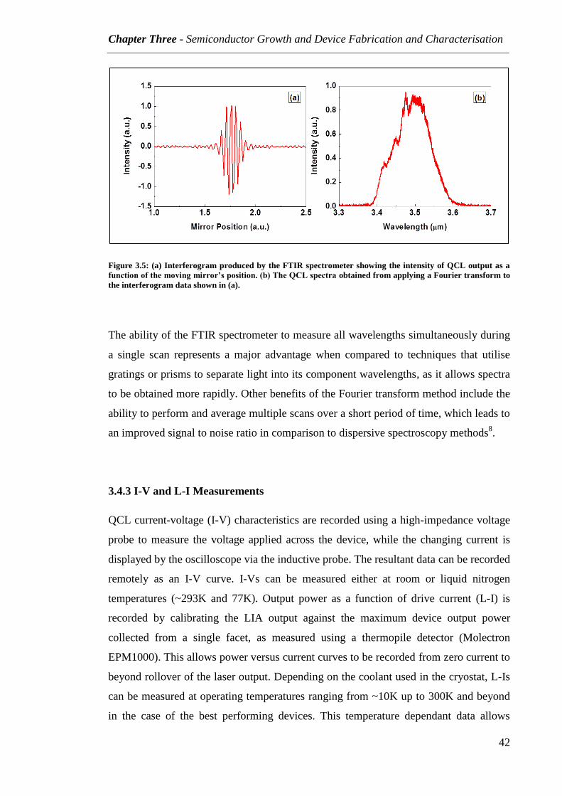
Chapter Three - Semiconductor Growth and Device Fabrication and Characterisation
42
Figure 3.5: (a) Interferogram produced by the FTIR spectrometer showing the intensity of QCL output as a
function of the moving mirror’s position. (b) The QCL spectra obtained from applying a Fourier transform to
the interferogram data shown in (a).
The ability of the FTIR spectrometer to measure all wavelengths simultaneously during
a single scan represents a major advantage when compared to techniques that utilise
gratings or prisms to separate light into its component wavelengths, as it allows spectra
to be obtained more rapidly. Other benefits of the Fourier transform method include the
ability to perform and average multiple scans over a short period of time, which leads to
an improved signal to noise ratio in comparison to dispersive spectroscopy methods8.
3.4.3 I-V and L-I Measurements
QCL current-voltage (I-V) characteristics are recorded using a high-impedance voltage
probe to measure the voltage applied across the device, while the changing current is
displayed by the oscilloscope via the inductive probe. The resultant data can be recorded
remotely as an I-V curve. I-Vs can be measured either at room or liquid nitrogen
temperatures (~293K and 77K). Output power as a function of drive current (L-I) is
recorded by calibrating the LIA output against the maximum device output power
collected from a single facet, as measured using a thermopile detector (Molectron
EPM1000). This allows power versus current curves to be recorded from zero current to
beyond rollover of the laser output. Depending on the coolant used in the cryostat, L-Is
can be measured at operating temperatures ranging from ~10K up to 300K and beyond
in the case of the best performing devices. This temperature dependant data allows

Chapter Three - Semiconductor Growth and Device Fabrication and Characterisation
43
calculation of a device’s characteristic temperature T0, which describes the rate of
increase of threshold current density with temperature.
3.4.4 Waveguide Losses
The waveguide losses αw, associated with a particular wafer design can be determined
experimentally by measurement of the threshold current density Jth, of a series of
devices of differing length. The threshold current density expressed in terms of the
device losses is given by9:
(3.4)
where αm and αw are the mirror and waveguide losses respectively, Γ is the waveguide
confinement factor and g is the gain coefficient - defined as the peak material gain per
unit threshold current density i.e. g=Gp/Jth. The mirror losses are dependent both upon
the reflectivities R1 and R2 of the laser facets and the length L, of the laser cavity:
( )
(3.5)
Substitution of equation 3.5 into 3.4 allows the threshold current density to be expressed
as a function of device length:
( )
(3.6)

Chapter Three - Semiconductor Growth and Device Fabrication and Characterisation
44
It can be seen therefore that measuring the threshold current of devices of different
length and plotting Jth against 1/L should yield a linear relationship with:
( )
and
(3.7a and 3.7b)
The facet reflectivities R1 and R2 are both assumed to be approximately 30%, and so an
estimate of the quantity gΓ can be made from the gradient. This can then in turn be used
in equation 3.7b to calculate αw.
3.4.5 Characteristic Temperature - T0
The evolution of a device’s threshold current density with increasing temperature can be
conveniently described by the parameter T0 - its characteristic temperature. It is
generally found that Jth increases exponentially over a well-defined temperature range
which can be described by the relationship10
:
( ) (
)
(3.8)
It can be seen from equation 3.8 that T0 can be extracted from a linear fit of the natural
logarithm of Jth plotted against T, over the temperature range for which the relationship
holds. Higher values of T0 are indicative of a threshold current density that increases
more slowly with temperature, and vice versa for low T0. For devices that operate at
high temperatures and/or in the CW regime, a low initial Jth coupled with a high T0 is
desirable in order to minimise the high operating temperatures associated with large
drive currents. Characteristic temperatures of the order of 100K are typical for the
GaAs-based devices presented in this thesis.

Chapter Three - Semiconductor Growth and Device Fabrication and Characterisation
45
1. National Centre for III-V Technologies [Online], Availiable at: http://www.epsrciii-
vcentre.com/Home.aspx, (2013).
2. M. A. Herman, W. Richter and H. Sitter, Epitaxy: Physical Principles and Technical
Implementation, (Springer, 2004).
3. G. B. Stringfellow, A critical appraisal of growth mechanisms in MOVPE, Journal of Crystal
Growth, 68, 111-122, (1984).
4. Clean Rooms - ISO Standard 14644 [Online], Availiable at:
http://www.engineeringtoolbox.com/clean-rooms-iso-d_933.html, (2013).
5. S. Franssila, Introduction to Microfabrication, (Wiley, 2010).
6. E. Huys, A Short Introduction to FTIR, (Bruker Optik).
7. T. J. Johnson and G. Zachmann, Introduction to Step-scan FTIR, (Bruker Optik).
8. J. F. James, A Student's Guide to Fourier Transforms: With Applications in Physics and
Engineering, (Cambridge University Press, 1995).
9. J. Faist, F. Capasso, D. L. Sivco, C. Sirtori, A. L. Hutchinson and A. Y. Cho, Quantum Cascade
Laser, Science, 264, 553-556, (1994).
10. C. Gmachl, F. Capasso, D. L. Sivco and A. Y. Cho, Recent progress in quantum cascade lasers
and applications, Reports on Progress in Physics, 64, 1533-1601, (2001).

46
Chapter Four
GaAs-based QCLs with InGaP and
InAlP Waveguides
4.1 Introduction
The chapter begins with a brief review of the work carried out at the University of
Sheffield on GaAs-based QCLs that is directly relevant to the studies presented in the
experimental chapters of this thesis. Following on from this, several new GaAs-based
QCL wafer designs are presented, into which both InGaP and InAlP have been
incorporated as a waveguide material. These designs represent a continuation of the
work previously undertaken at Sheffield, as well as an attempt to further enhance the
performance levels achievable from GaAs QCLs. The operating characteristics of
devices fabricated from these wafers are then presented and analysed, with comparisons
made to previous GaAs-based lasers.
4.2 GaAs-based QCLs: Sheffield Progress
The study of GaAs-based QCLs at the University of Sheffield spans a timeframe of over
a decade and has touched upon several different areas of development, from
fundamental studies of the electron distribution within the QCL core region1 to more
applied areas such as the development of MOVPE growth of GaAs-based devices2. Of
particular relevance to the work presented in this thesis, are the investigations that were
carried out by physicists at Sheffield that sought to optimise device performance
through adaptation of the laser waveguide. As will be discussed in more detail shortly,
GaAs-based QCLs generally make use of either highly doped GaAs or high aluminium

Chapter Four - GaAs-based QCLs with InGaP and InAlP Waveguides
47
content AlGaAs layers to form the device waveguide, both of which have their relative
merits and limitations.
As an alternative to these materials, Green and co-workers designed and fabricated a
GaAs/Al0.45Ga0.55As QCL that incorporated an In0.49Ga0.51P waveguide3, which it was
hoped would improved device performance through both the increased confinement of
the optical mode within the core region, and lower waveguide losses. When
characterised, this device was seen to operate up to 305K - the first time room-
temperature operation of a GaAs-based QCL had been observed at Sheffield, and a
considerable improvement in the 190K maximum operating temperature measured for
previous GaAs/AlGaAs devices4. Although the threshold current density of ~6kA/cm
2
at 77K represented an increase of ~1.5kA/cm2 in comparison to earlier lasers
5, operating
voltages were found to be near identical to previous devices. These encouraging results
appeared to confirm the potential of InGaP waveguides for enhancing GaAs-based QCL
performance.
Following on from this work, Krysa et al grew a similar GaAs/AlGaAs QCL structure
with InGaP waveguide, but using MOVPE rather than MBE which had been used for all
previous QCL growth6. The structure itself was modified somewhat in an attempt to
optimise performance and further reduce optical losses within the device core, with the
design changes including a doubling of the waveguide thickness to 3µm and a reduction
in doping to N=5x10¹⁶
cm-3
. An additional GaAs cladding layer was also inserted
between the lower waveguide and GaAs substrate. These refinements resulted in
devices that again demonstrated operation at room temperature, but with greatly
enhanced optical and electrical characteristics than those observed previously. Room-
temperature threshold current density and peak output power from a 4mm-long, high-
reflection coated device were found to be 6.5kA/cm2 and 220mW respectively, with an
emission wavelength of λ~9µm. In comparison, the previous InGaP laser could only
achieve a room-temperature Jth of ~32kA/cm2 and peak output power of the order of
several milliwatts.
These results represented excellent progress in improving GaAs QCL performance in
terms of the threshold currents that could be achieved from devices, which were the
lowest Jth observed at room-temperature at the time. However, as a conclusion to the
study it was suggested that performance might be further enhanced through the use of

Chapter Four - GaAs-based QCLs with InGaP and InAlP Waveguides
48
InAlP as a waveguide material, due to its lower refractive index compared to InGaP and
therefore greater potential for optical confinement. It is this juncture that marks the
starting point for the work presented in these experimental chapters.
4.3 Phosphide Materials as QCL Waveguides
QCL performance is strongly dependent upon the efficiency with which the optical
mode can be confined to the device core region. For example, as was seen in chapter
two, the threshold current density is inversely proportional to the device modal gain
(defined as the material gain multiplied by the mode confinement factor Γ), and directly
proportional to the waveguide loss αw (expressed within the total cavity losses αtot).
Maximising the overlap of the optical mode with the device core allows the modal gain
to be increased, while decreasing αw by reducing the proportion of the optical mode that
reaches the material layers that constitute the rest of the structure. As with the majority
of semiconductor lasers, QCL devices achieve this overlap by utilising waveguide
layers that have a lower refractive index than the core region they surround, with the
refractive index contrast providing the mechanism for confinement of the light
generated within the active region.
In the case of the earliest GaAs-based QCLs, the waveguide layers were provided by
high-Al fraction Al0.9Ga0.1As7, which possessed a relatively high refractive index
contrast with the GaAs/AlGaAs core region and exhibited low optical losses at the
emission wavelength of λ=9.4µm. Additionally, the waveguide layer thicknesses of
≲1µm meant the overall thickness of the device structure was minimised. Several
drawbacks to the use of Al0.9Ga0.1As were soon discovered however, including a large
variation in device threshold current and output power under illumination with white
light at low temperature8. This behaviour was found to result from the release of
electrons from DX centres within the waveguide layers causing a subsequent increase in
waveguide losses. The low electron mobility and electrical conductivity were also cited
as potential drawbacks associated with this material system. In an attempt to overcome
these limitations, later GaAs devices employed a waveguide consisting of layers of
highly doped GaAs9, which utilised the large drop in refractive index that occurs at
wavelengths corresponding to the material’s plasma frequency. The plasma frequency

Chapter Four - GaAs-based QCLs with InGaP and InAlP Waveguides
49
and refractive index of the waveguide layer can be tailored through changes to its
doping level, which can be of the order of N~1018
cm-3
at infrared wavelengths. Other
advantages of using GaAs over AlGaAs include the lower demands placed on wafer
growth6 and the lower thermal conductivity of the binary compound compared to the
ternary AlGaAs alloy.
The use of GaAs as a waveguide material has to-date proven sufficient to enable GaAs-
based devices to achieve performance levels ranging from low-temperature CW10,11
to
room-temperature pulsed12
operation. There are however, several perceived
disadvantages to the use of GaAs that make the investigation of new waveguide
materials a worthwhile endeavour. For example, the high doping levels required must be
precisely controlled during growth in order to achieve the required refractive index,
with small fluctuations able to cause a large shift from the desired index. The highly
doped layers can also lead to increased free-carrier absorption of the optical mode, and
so thick low-doped GaAs layers are grown surrounding the core in order to spatially
separate the mode from the waveguide. This can substantially increase the total
thickness of the device structure.
As a response to these shortcomings, the idea of using phosphide-containing alloys as a
waveguide material in GaAs-based QCLs has been suggested3,6
, and studies of the
performance of such devices make up the majority of the work presented in this thesis.
The two alloys in question - InGaP and InAlP - have various characteristics that make
them promising candidates for such an application. Both have a refractive index contrast
with GaAs/AlGaAs sufficient for a large confinement of the optical mode at infrared
wavelengths, while the lack of need for high doping to achieve their low refractive
indices means InGaP and InAlP do not suffer from the large free-carrier losses
associated with GaAs waveguides. This removes the need to have thick spacer layers
surrounding the core region and allows the thickness of the device structure to be kept
comparatively low. Additionally - for InGaP at least - good electrical characteristics
should be facilitated by the InGaP/GaAs conduction band offset of 0.16eV13
, a point
that will be discussed in detail later in this thesis.
In order to compare the levels of optical confinement and loss that these different
waveguide materials might provide, figures 4.1 to 4.4 show a series of TM optical mode
profiles for four different waveguide structures surrounding an identical GaAs/AlGaAs

Chapter Four - GaAs-based QCLs with InGaP and InAlP Waveguides
50
core region, calculated for emission at a wavelength of 9µm. The method used to
produce the profiles is described in detail in chapter two and appendix A.2. Figures 4.1
and 4.2 detail QCL structures with waveguides comprising of Al0.9Ga0.1As and highly-
doped GaAs respectively, and are based on designs presented in references [7] and [9].
Although these structures are not optimised for the core region in question, the emission
wavelength is close enough to that of the original design that the calculated confinement
and losses are very similar. Figures 4.3 and 4.4 show the same core region, but the
AlGaAs and GaAs waveguide layers have been replaced with InGaP and InAlP
respectively.
Starting with the Al0.9Ga0.1As waveguide structure below in figure 4.1, it can be seen
that for a refractive index contrast of Δnref=0.4, an optical confinement of Γ=63% could
be expected for a wavelength of λ=9µm. Despite the GaAs spacer layers surrounding
the core region, approximately 4% of the optical mode penetrates into the waveguide
layers resulting in a waveguide loss of αw=13cm-1
.
-9 -8 -7 -6 -5 -4 -3 -2 -1 0 10.0
0.2
0.4
0.6
0.8
1.0
1.2
0.0
0.5
1.0
1.5
2.0
2.5
3.0
3.5
Ga
As
N=
4x
10
16
Su
bs
tra
te
N=
3x
10
18cm
-3
w = 13cm-1
= 63%
= 9m Ga
As
N =
9x
10
18
Al 0
.9G
a0.1A
s N
= 6
x1
017
GaAs
GaAs
Mo
de I
nte
nsit
y (
a.u
.)
Distance (m)
CoreGaAs
Al 0
.9G
a0.1A
s N
= 6
x1
017
Ga
As
N=
4x
10
16
Refr
ac
tive
In
dex
Figure 4.1: TM optical mode profile detailing the calculated mode intensity (left-hand axis) and waveguide
refractive index (right-hand axis) for a QCL device operating at 9µm and featuring an Al0.9Ga0.1As waveguide
structure taken from reference [7]. Doping levels for all profiles are given in cm-3.
In figure 4.2 the Al0.9Ga0.1As layers have been replaced with highly-doped
(N=6x10¹⁸
cm-3
) GaAs. Although there is a large refractive index contrast between the

Chapter Four - GaAs-based QCLs with InGaP and InAlP Waveguides
51
high-doped GaAs layers and the core region (Δnref~1.2), the optical confinement of
Γ=42% afforded by the GaAs waveguide is relatively low in comparison to the AlGaAs
design. This is mainly due to the comparatively thick (3.5µm) GaAs spacer layers that
are required to spatially separate the optical mode from the highly-doped (and thus
highly lossy) GaAs waveguide layers. Although optical confinement within the core is
lower, the spacer layers ensure very little of the mode penetrates the waveguide (~0.5%)
and thus losses are reduced to αw=11cm-1
.
-14 -12 -10 -8 -6 -4 -2 00.0
0.2
0.4
0.6
0.8
1.0
1.2
0.0
0.5
1.0
1.5
2.0
2.5
3.0
3.5
Su
bs
tra
te
N=
3x
10
18cm
-3
Ga
As
N =
5x
10
16
Ga
As
N =
5x
10
16
w = 11cm-1
= 42%
= 9m
GaAs
GaAs
Mo
de
In
ten
sit
y (
a.u
.)
Distance (m)
CoreGaAsG
aA
s N
= 6
x1
018
Ga
As
N =
6x
10
18
Re
fra
cti
ve
In
de
x
Figure 4.2: TM mode profile for the same core region as featured in figure 4.1, but with a highly-doped
(N=6x1018cm-3) GaAs waveguide taken from reference [9].
By replacing the GaAs waveguide layers with In0.49Ga0.51P, a large increase in optical
confinement can be attained, illustrated by the mode profile shown in figure 4.3. The
GaAs spacer layers (shown as the blue hatched areas surrounding the core) are primarily
included to increase the refractive index contrast with the waveguide (Δnref=0.25),
rather than to separate the mode from the InGaP layers which are low-doped, and so not
expected to contribute to free-carrier loss. The refractive index contrast combined with
the thin GaAs spacer means optical confinement is increased to Γ=62%, while only
~0.2% of the mode is able to reach the outer layers of the structure. This results in a
correspondingly low waveguide loss of αw=6cm-1
.
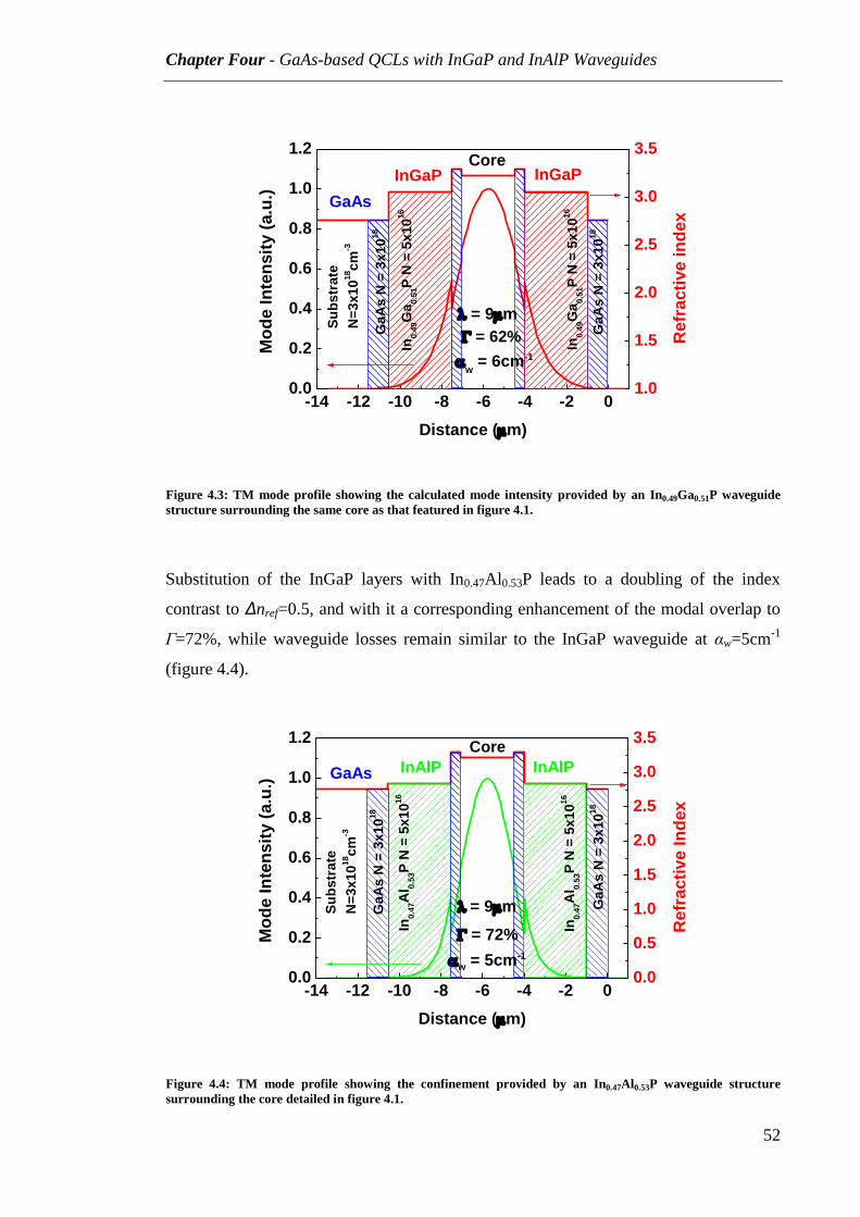
Chapter Four - GaAs-based QCLs with InGaP and InAlP Waveguides
52
-14 -12 -10 -8 -6 -4 -2 00.0
0.2
0.4
0.6
0.8
1.0
1.2
1.0
1.5
2.0
2.5
3.0
3.5
In0.4
9G
a0.5
1P
N =
5x
10
16
Su
bs
tra
te
N=
3x
10
18cm
-3
In0.4
9G
a0.5
1P
N =
5x
10
16
Ga
As
N =
3x
10
18
Ga
As
N =
3x
10
18
InGaP
Mo
de In
ten
sit
y (
a.u
.)
Distance (m)
InGaPCore
GaAs
= 9m
w = 6cm-1
= 62%
Re
fra
cti
ve in
dex
Figure 4.3: TM mode profile showing the calculated mode intensity provided by an In0.49Ga0.51P waveguide
structure surrounding the same core as that featured in figure 4.1.
Substitution of the InGaP layers with In0.47Al0.53P leads to a doubling of the index
contrast to Δnref=0.5, and with it a corresponding enhancement of the modal overlap to
Γ=72%, while waveguide losses remain similar to the InGaP waveguide at αw=5cm-1
(figure 4.4).
-14 -12 -10 -8 -6 -4 -2 00.0
0.2
0.4
0.6
0.8
1.0
1.2
0.0
0.5
1.0
1.5
2.0
2.5
3.0
3.5
In0.4
7A
l 0.5
3P
N =
5x
10
16
In0.4
7A
l 0.5
3P
N =
5x
10
16
Ga
As
N =
3x
10
18
Ga
As
N =
3x
10
18
Su
bs
tra
te
N=
3x
10
18cm
-3
InAlP
Mo
de In
ten
sit
y (
a.u
.)
Distance (m)
InAlPGaAs
Core
= 9m
= 72%
w = 5cm-1
Re
fra
cti
ve In
dex
Figure 4.4: TM mode profile showing the confinement provided by an In0.47Al0.53P waveguide structure
surrounding the core detailed in figure 4.1.
Chapter Four - GaAs-based QCLs with InGaP and InAlP Waveguides
53
These calculations demonstrate the potential that both InGaP and InAlP have for use as
low-loss QCL waveguides that offer high optical confinement at infra-red wavelengths.
The materials are lattice matched to GaAs for the compositions In0.49Ga0.51P and
In0.47Al0.53P, and can be easily incorporated into typical GaAs-based QCL structures
using MOVPE. The experimental results detailed in the following sections will
demonstrate this potential by showing the performance enhancements, particularly in
regard to threshold current, that can be achieved in devices that utilise these two
materials as waveguide layers.
4.4 GaAs/AlGaAs QCLs with InGaP and InAlP
Waveguides
Following on from the work by Krysa et al, a series of four QCL wafers incorporating
either InGaP or InAlP waveguide layers were grown in order to investigate whether the
performance of GaAs QCLs could indeed be enhanced via further modification to the
waveguide. The wafers are given the designations MR2784, MR2785, MR2789 and
MR2790, with the general layer structure of each wafer shown in figure 4.8. By
producing a series of wafers with differing designs, it is possible to investigate the effect
that changes in either the active region or waveguide (or in some cases both) have on
laser performance. For example, wafer MR2784 is essentially a copy of the design of
the laser with InGaP waveguide presented in section 4.2, with minor alterations to the
core region. Wafer MR2789 on the other hand incorporates a completely new InAlP
waveguide whilst keeping unchanged the core region design of MR2785 (which has an
InGaP waveguide) allowing for comparison between the two material systems. A
detailed discussion of the design approach for each wafer is given in the following
section, which includes descriptions of the complete wafer structure, core region design
and the electronic wavefunctions associated with device operation.

Chapter Four - GaAs-based QCLs with InGaP and InAlP Waveguides
54
4.5 Wafer Design
In common with wafers grown for the previous work on GaAs lasers with InGaP
waveguides (described in section 4.2), all QCL structures were grown on an N+ (100)
GaAs substrate (N=3x10¹⁸
cm-3
) with a 10° miscut toward the (111) plane. These non-
standard substrates are necessary to mitigate the effects of Cu-type atomic ordering in
the InGaP and InAlP layers3. A low-pressure, horizontal-flow MOPVE reactor
operating at 690°C for InGaP growth and 710°C for InAlP growth was used, and each
structure was grown in a single run.
MR2784
By way of acting as a reference to our group’s previous QCLs with InGaP
waveguides, wafer MR2784 incorporated a GaAs/Al0.45Ga0.55As core region identical to
that featured in the device detailed in section 4.2, designed to emit at λ~9µm. The
number of core region repeat periods however, was increased from 36 to 55 in order to
increase the overlap of the optical mode with the core region and thus also the optical
gain. By increasing this core region overlap it was also hoped that the optical mode
would penetrate less into the highly doped outer cladding layers of the wafer, leading to
an overall decrease in the waveguide losses. Calculations of these parameters for
MR2784 show that an optical confinement of Γ~62% may be expected, an increase
from the Γ~42% estimated for the previous device with its narrower core region, while
waveguide losses are also decreased - αw=5.7cm-1
compared to αw=9.5cm-1
. All other
wafers described in this section have 55 repeat periods of their respective core regions.
Starting from the GaAs substrate, the layer sequence for MR2784 was: 1µm highly-
doped (N=3x10¹⁸
cm-3
) GaAs, 3µm In0.49Ga0.51P (N=5x10¹⁶
cm-3
) waveguide and 0.5µm
GaAs spacer layer (N=5x10¹⁶
cm-3
). The 55 period (2.54µm) core region follows, and
the layer sequence then continues with a repeat of the 0.5µm GaAs spacer, 3µm InGaP
waveguide and 1µm GaAs layer to complete the structure. The Γ-point conduction band
profile for the core region of MR2784, including the moduli squared of the electronic
wavefunctions is shown in figure 4.5, where the wavefunction Eu corresponds to the
upper laser level, El to the lower laser levels and Ei to the injection level. The dipole

Chapter Four - GaAs-based QCLs with InGaP and InAlP Waveguides
55
matrix element for the diagonal optical transition between Eu and El was calculated to
be zij=2.4nm.
Figure 4.5: Γ-point conduction band profile for the core region of sample MR2784 under a bias of 48kV/cm2.
The profile includes the moduli-squared of the electronic wavefunctions associated with the optical transition
(Eu and El in red), the injector level (EI in blue) and the injector miniband (black).
The sequence of wells and barriers that constitutes one complete period of
core region (i.e. one active and one injector region) is as follows
(where thicknesses are given in nm and begin at the injection barrier):
4.5/2.0/1.1/5.4/1.1/4.8/2.6/3.8/1.7/3.4/1.8/3.2/2.0/3.0/2.6/3.0. Normal font represents the
GaAs quantum wells, bold font the Al0.45Ga0.55As barriers and underlined layers are
Si-doped (N=4x10¹⁷
cm-3
).
0 10 20 30 40 50 60 701.0
1.2
1.4
1.6
1.8
2.0
En
erg
y (
eV
)
Distance (nm)
Eu
Ei
Eu
El

Chapter Four - GaAs-based QCLs with InGaP and InAlP Waveguides
56
MR2785
Wafer MR2785 follows the same general layer structure as MR2784, but with an altered
core region design that attempts to increase gain by shifting from the diagonal optical
transition used previously, to a more vertical transition within the second active region
quantum well.
The layer sequence that makes up the active and injector regions is as follows:
4.2/1.7/1.0/5.8/1.0/5.2/2.6/4.0/1.7/3.7/1.8/3.3/2.0/3.1/2.6/3.0, where the character
formatting follows the convention described previously. Comparing this core region
sequence to that of wafer MR2784, several modifications can be observed. Firstly, the
width of the first quantum well has been reduced from 2.0nm to 1.7nm, while the
surrounding barriers have also been slightly reduced in thickness. Additionally, the
second and third quantum wells that make up the remainder of the active region have
been widened to 5.8nm and 5.2nm, from 5.4nm and 4.8nm respectively, with only
minor alterations to the associated barriers. Modifications to the injector section of the
core region include a widening of the first four quantum wells by 0.2nm, 0.3nm, 0.1nm
and 0.1nm respectively, while all injector region barriers remain unchanged.
Figure 4.6 shows the conduction band profile for the core region of MR2785. It can be
seen that the primary effect of narrowing the first active region quantum well is to allow
the wavefunction associated with the upper laser level Eu, to penetrate further into the
second well, reducing the resonance with the injector level Ei but increasing the
resonance with the lower laser level El. As described in chapter two, this more vertical
transition is expected to have a larger dipole matrix element than the previous diagonal
transition, which can result in a larger associated intersubband gain. Calculations show
that the matrix element for the optical transition associated with this active region
design is zij=2.7nm, an increase from zij=2.4nm calculated for MR2784. It is possible
therefore that several enhancements in device performance may result, such as a lower
threshold current and increased output power14
. As was discussed in chapter 2 however,
vertical transitions also result in a lower population inversion between subbands and can
thus act to reduce the intersubband gain and subsequently lower device performance.
The success or otherwise of this vertical transition design will be discussed in the
section detailing device performance.

Chapter Four - GaAs-based QCLs with InGaP and InAlP Waveguides
57
0 10 20 30 40 50 60 70 801.0
1.2
1.4
1.6
1.8
2.0 Eu
En
erg
y (
eV
)
Distance (nm)
El
Eu
Ei
Figure 4.6: Γ-point conduction band profile for the core region of sample MR2785 under a bias of 48kV/cm2,
including the electronic wavefunctions relevant to the optical transition.
MR2789
Wafer MR2789 features the same core region design as that of MR2785 above, but with
an InAlP waveguide replacing the previous InGaP layer. Calculations suggest that the
optical confinement afforded by the InAlP should increase to ~74% compared to 63%
for the InGaP waveguide, while the waveguide loss decreases from 5.7cm-1
previously
to 4.8cm-1
. A summary of the confinement factor and waveguide losses expected for
each individual device is presented in table 4.1. The effect of this theoretical increase in
confinement, along with the corresponding changes in performance of lasers fabricated
from the two wafers is outlined in section 4.6 which presents individual laser
characteristics.
Beginning from the N+ GaAs substrate, the complete wafer structure of MR2789 was:
1µm of highly-doped (N=3x10¹⁸
cm-3
) GaAs, 3µm In0.47Al0.53P waveguide layer
(N=5x10¹⁶
cm-3
), 0.2µm GaAs spacer layer (N=5x10¹⁶
cm-3
) followed by the 55-period
GaAs/Al0.45Ga0.55As core region. The cladding layer sequence is then repeated in
reverse to complete the structure. With the InAlP waveguide effectively acting as an
electronic barrier with a height of ~0.31eV15
, a ‘transitional layer’ (TL) was positioned
between each GaAs/InAlP interface (see figure 4.8) in order to reduce the abruptness of

Chapter Four - GaAs-based QCLs with InGaP and InAlP Waveguides
58
the barrier at these points and aid electron flow through the structure. This layer
consisted of 25nm of In0.49Ga0.51P followed by 16nm of In(Ga0.5Al0.5)0.5P
(5x10¹⁶
cm-3
≤ N ≤ 1x10¹⁷
cm-3
) when transitioning from GaAs to the InAlP waveguide,
while the sequence was reversed when transitioning from InAlP to GaAs.
MR2790
Finally, wafer MR2790 duplicates the cladding structure of MR2789 while modifying
the active region to incorporate an extra quantum well, thus resulting
in a double-phonon relaxation design. One complete period incorporating the
active and injector region (beginning from the injection barrier) is as follows:
4.2/1.8/0.9/5.2/0.9/5.0/0.9/4.7/2.2/3.6/1.7/3.5/1.7/3.3/1.8/3.1/2.1/2.9/2.7/2.9, with the
numbering following the usual convention. The conduction band profile for MR2790 is
shown below in figure 4.7, and illustrates the additional lower laser level that results
from the addition of the fourth active region quantum well. These three lower levels
constitute the double-LO-phonon relaxation design discussed in chapter one. The
calculated optical matrix element of zij=3.3nm for this particular active region design
represents an increase in comparison to MR2785 and MR2789.
0 10 20 30 40 50 60 70 80 901.0
1.2
1.4
1.6
1.8
2.0 Eu
En
erg
y (
eV
)
Distance (nm)
Eu
Ei
El
Figure 4.7: Γ-point conduction band profile for the core region of sample MR2790 under a bias of 48kV/cm2.
The profile illustrates the extra lower laser level (El in red) that results from the inclusion of a fourth quantum
well in the active region.

Chapter Four - GaAs-based QCLs with InGaP and InAlP Waveguides
59
As with wafer MR2789, 25/16nm InGaP/InGaAlP transitional layers were positioned
between each GaAs/InAlP interface in order to aid electron flow through devices.
Design Summary
Shown in table 4.1 is a summary of the design features of each wafer, while table 4.2
lists the bandgap and conduction band offset with respect to GaAs for each waveguide
material. Overleaf, figure 4.8 features a schematic diagram showing the layer structure
for wafers featuring the InGaP (MR2784/85) and InAlP (MR2789/90) waveguides.
Sample Active Region
Design
Waveguide
Material
Confinement
Factor - Γ
(%)
Waveguide
Loss - αw
(cm-1
)
MR2784
Single-phonon
Diagonal
transition
In0.49Ga0.51P 62 5.7
MR2785
Single-phonon
‘Vertical’
transition
In0.49Ga0.51P 63 5.7
MR2789
Single-phonon
‘Vertical’
transition
In0.47Al0.53P 74 4.8
MR2790
Double-phonon
‘Vertical’
transition
In0.47Al0.53P 81 4.8
Table 4.1: Design summary outlining the features of each sample described in the preceding sections,
highlighting the differing optical confinement and waveguide losses expected for each waveguide design at an
emission wavelength of λ=9µm.
Waveguide Material Bandgap (eV) Conduction Band Offset
With Respect To GaAs (eV)
In0.49Ga0.51P 1.91 (Direct)13
0.1613
In0.47Al0.53P 2.38 (Indirect)13
0.3115
Table 4.2: Key band parameters for the InGaP and InAlP waveguides featured in the QCL designs presented
in this, and subsequent chapters.

Chapter Four - GaAs-based QCLs with InGaP and InAlP Waveguides
60
Figure 4.8: Schematic illustration of the semiconductor structure for each wafer, including transitional layers.
4.6 Device Performance
4.6.1 Spectra
Shown in figure 4.9 are the emission spectra obtained from 2mm as-cleaved lasers,
taken at 300K using a Fourier transform infrared spectrometer at a resolution of 1cm-1
.
Device MR2784 is observed to lase at a wavelength of λ=9.08µm, close to the intended
λ~9µm design wavelength of this sample as well as that of the InGaP laser presented
previously in section 4.2. This is as expected, considering the identical active region
design (albeit with an increased number of core region repeat periods) shared by the two
devices. The active regions of devices MR2785 and MR2789 are also identical - sharing
the same vertical transition design outlined previously - and as such exhibit operating
wavelengths of λ=8.82µm and λ=8.63µm respectively. Finally MR2790, which employs
a modified double-phonon active region, displays emission at λ=9.72 µm.

Chapter Four - GaAs-based QCLs with InGaP and InAlP Waveguides
61
The similarity of emission wavelength between samples with the same active region
design, combined with the ability to accurately reproduce the performance of historical
devices (i.e. MR2784 and the device presented by Krysa et al) gives confidence in the
overall quality and calibration accuracy of the MOVPE growth used to fabricate
individual wafers. The wavelength discrepancy between the samples with the longest
and shortest emission wavelengths (MR2789 and MR2790), corresponds to an energy of
Eλ~16meV, which of the order of a typical GaAs QCL gain spectrum.
900 950 1000 1050 1100 1150 1200
11 10.5 10 9.5 9 8.5
No
rmalis
ed
In
ten
sit
y (
a.u
.)
Wavenumber (cm-1)
MR2784:
=9.08m
MR2785:
=8.82m
MR2789:
=8.63m
MR2790:
=9.72m
Design =9m
Wavelength (m)
Figure 4.9: Combined spectra showing the room-temperature emission wavelength for 2mm-long, 20µm-wide
devices fabricated from each wafer.
4.6.2 Optical and Electrical Performance
A series of 2mm and 3mm-long as-cleaved lasers were characterised under pulsed
operation, at a repetition rate of 5kHz and pulse width of 50ns using the techniques
described in chapter 3. Due to the high incidence of device failure in some of the
samples, the performance data quoted in this and subsequent experimental chapters
represents the best performance from a single device rather than an average of several.
The threshold current densities quoted throughout the following chapters have an
associated uncertainty of ~ ±10%, due to the uncertainties in the width of the laser
ridges (which showed evidence of undercutting of the ridge pattern during the etching

Chapter Four - GaAs-based QCLs with InGaP and InAlP Waveguides
62
process), and the variations in the current pulse shape and position of the oscilloscope
gate during measurement. Results are presented below for each individual wafer
design.
MR2784
Figure 4.10 shows the typical light-current characteristics for a 2mm-long, 20µm-wide
laser fabricated from wafer MR2784. This data, along with the majority of L-I curves
presented in this work are typical of most QCL devices. As the bias across the device is
increased, the electronic states associated with the optical transition align with the
injector miniband enabling efficient electron flow through the device and eventual
lasing. Subsequent increases in electrical current result in a concomitant rise in optical
output power, as the rate at which electrons are injected into the device core increases
along with the active region population inversion. After a time however, the continued
increase in bias across the laser core causes the electronic states to become misaligned,
resulting in a significant reduction in injection efficiency into the upper laser level and
thus a decrease in optical output power - referred to as rollover.
As expected, since the active region designs of MR2784 and the InGaP laser of Krysa et
al are nominally identical, the performance of MR2784 shares common characteristics
with this device. It has already been noted that the room-temperature emission
wavelength of both is similar - 9.08µm (MR2784) compared to 9.2µm previously,
however both the temperature range over which the devices operate, and their threshold
current densities also display similar values. At 240K, a threshold current density of
4.4kA/cm2 is observed for device MR2784, rising to 8.2kA/cm
2 at 300K. This is in
comparison to 4.5kA/cm2 and 8.0kA/cm
2 at 240K and 300K respectively for the
previous InGaP device. The maximum temperature of operation increases slightly to
340K, up from 320K previously.

Chapter Four - GaAs-based QCLs with InGaP and InAlP Waveguides
63
2 4 6 8 10 12 14 16 180.0
0.2
0.4
0.6
0.8
1.0
1.2
1.4
1.6
1.8
2.0
8.5 9.0 9.5 10.0
Peak o
pti
cal
po
wer
(W)
Current density (kA/cm2)
240K
260K
280K
300K
320K
340K
Wavelength (m)
=9.08m
Figure 4.10: Peak output power vs. drive current for a 2mm-long 20µm-wide device fabricated from wafer
MR2784. Inset: High-resolution (0.5cm-1) FTIR spectra showing emission at 9.08µm for the same device.
While the threshold currents for MR2784 and the previous InGaP laser are comparable
over the entire operating temperature range, a large increase in peak optical output
power (as measured from a single facet) is observed for the new device. At 240K, a
maximum output power of 1.58W is observed - an increase of over 1W compared to
that reported by Krysa et al at the same temperature. At 300K, MR2784 continued to
deliver 0.56W of power, compared to 0.11W previously. A second 3mm-long, 20µm-
wide device fabricated from wafer MR2784 exhibited similar threshold current
densities, with Jth=4.3kA/cm2 at 240K and 8.0kA/cm
2 at 300K, however the output
power, particularly at 240K, was substantially lower compared to the 2mm laser.
Powers of 0.73W and 0.32W at 240K and 300K respectively were observed, although it
should be noted that the maximum current with which the 3mm device was driven was
reduced to ~11kA/cm2 to prevent premature device failure. The greater observed output
power seen for MR2784, when compared to the previous InGaP QCL, could be
attributed to the increase in the number of active region periods from 36 to 55. The
negligible reduction in threshold current density that is observed between the devices
however, lends uncertainty to this conclusion since (from equation 3.4) we would
expected a lowering of Jth due to the increased modal overlap in the wider core region
of MR2784.

Chapter Four - GaAs-based QCLs with InGaP and InAlP Waveguides
64
Shown in figure 4.11 below is an exponential fit of the threshold current density versus
temperature data for the 2mm device, with the associated value for the characteristic
temperature T0. It is found that this fit can be applied to both 2mm and 3mm lasers over
the entire temperature range of operation, resulting in T0=95±11K and T0=99±13K
respectively.
220 240 260 280 300 320 340 3604
6
8
10
12
14Jth
(k
A/c
m2
)
Temperature (K)
T0=95K
Figure 4.11: Threshold current density vs. operating temperature for a 2mm-long, 20µm-wide device
fabricated from MR2784. The linear fit yields a value for the characteristic temerature, T0 of 95K.
MR2785
As discussed in section 4.4.1, MR2785 retains the cladding layer structure of MR2784
but has a modified active region, the details of which were also described earlier in the
chapter. L-I curves for a 3mm-long 20µm-wide laser are shown in figure 4.12, with the
associated dependence of threshold current density on operating temperature presented
in figure 4.13.

Chapter Four - GaAs-based QCLs with InGaP and InAlP Waveguides
65
4 5 6 7 8 9 10 11 12 130.0
0.1
0.2
0.3
0.4
0.5
0.6
0.7
0.8
0.9
1.0
8.5 9.0 9.5 10.0P
eak o
utp
ut
po
wer
(W)
Current Density (kA/cm2)
240K
300K
320K
260K
280K Wavelength (m)
=8.77m
Figure 4.12: Peak output power vs. drive current for a 3mm-long 20µm-wide device fabricated from wafer
MR2785. Inset: High-resolution (0.5cm-1) spectra showing emission at 8.77µm.
Despite the redesigned active region of MR2785, no performance enhancements are
observed when compared to devices fabricated from wafer MR2784. Threshold current
densities of 4.7kA/cm2 and 8.6kA/cm
2 are observed at 240K and 300K respectively -
consistent within experimental uncertainty to those observed for MR2784 at the same
temperatures. A 2mm-long device exhibits similar threshold currents of 4.9kA/cm2 and
9.2kA/cm2 at 240K and 300K respectively. Optical output powers are reduced - the
maximum peak power observed being 1.23W at 240K for a 2mm-long device, which
decreased to 0.36W at 300K. As seen in figure 4.12 above, this reduction in power is
also observed in the longer laser. It would appear from this general reduction in device
performance that the redesigned active region has resulted in a decreased electron
population inversion that outweighs the larger dipole matrix element associated with the
more vertical optical transition. This reduced population inversion has subsequently led
to a reduction in intersubband gain and the observed performance reductions for
MR2785. Characteristic temperatures extracted from Jth vs. T data yield T0=96±15K for
the 3mm laser and T0=93±14K for the 2mm device (see figure 4.13).
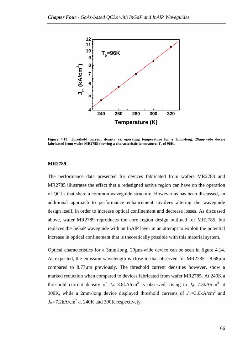
Chapter Four - GaAs-based QCLs with InGaP and InAlP Waveguides
66
240 260 280 300 3204
5
6
7
8
9
10
11
12
Jth
(k
A/c
m2)
Temperature (K)
T0=96K
Figure 4.13: Threshold current density vs. operating temperature for a 3mm-long, 20µm-wide device
fabricated from wafer MR2785 showing a characteristic temerature, T0 of 96K.
MR2789
The performance data presented for devices fabricated from wafers MR2784 and
MR2785 illustrates the effect that a redesigned active region can have on the operation
of QCLs that share a common waveguide structure. However as has been discussed, an
additional approach to performance enhancement involves altering the waveguide
design itself, in order to increase optical confinement and decrease losses. As discussed
above, wafer MR2789 reproduces the core region design outlined for MR2785, but
replaces the InGaP waveguide with an InAlP layer in an attempt to exploit the potential
increase in optical confinement that is theoretically possible with this material system.
Optical characteristics for a 3mm-long, 20µm-wide device can be seen in figure 4.14.
As expected, the emission wavelength is close to that observed for MR2785 - 8.68µm
compared to 8.77µm previously. The threshold current densities however, show a
marked reduction when compared to devices fabricated from wafer MR2785. At 240K a
threshold current density of Jth=3.8kA/cm2 is observed, rising to Jth=7.3kA/cm
2 at
300K, while a 2mm-long device displayed threshold currents of Jth=3.6kA/cm2 and
Jth=7.2kA/cm2 at 240K and 300K respectively.

Chapter Four - GaAs-based QCLs with InGaP and InAlP Waveguides
67
2 3 4 5 6 7 8 9 10 110.0
0.2
0.4
0.6
0.8
1.0
8.0 8.5 9.0 9.5
Peak o
utp
ut
po
wer
(W)
Current Density (kA/cm2)
240K
300K
320K
260K
280K
Wavelength (m)
=8.68m
Figure 4.14: Peak output power vs. drive current for a 3mm-long 20µm-wide device based on wafer MR2789.
Inset: High-resolution spectra showing emission at 8.68µm.
A peak optical output power of 0.83W was measured for the 3mm-long device at 240K,
falling to 0.20W at 300K, with the 2mm device displaying powers of 0.77W and 0.22W
at 240K and 300K respectively. A direct comparison of the output powers for MR2785
and MR2789 is difficult due to the lower maximum current density at which the devices
based on MR2789 were run - ~10kA/cm2 compared to ~15kA/cm
2 in the case of 2mm-
long lasers. This reduction was an attempt to mitigate the strong heating effects
produced by abnormally high operating voltages that resulted in a very high incidence
of device failure (see discussion later in this chapter). It can be seen however that in the
case of 2mm-long devices, an approximately 40% reduction in maximum drive current
results in a corresponding 40% reduction in peak output power, while a smaller ~15%
decrease for the 3mm-long laser leads to an almost identical power to its 3mm
counterpart from wafer MR2785. It can be surmised therefore that output powers are at
least unaffected by the introduction of the InAlP waveguide, and may be enhanced in
comparison. The maximum temperature of operation was 320K for both devices, similar
to MR2785, while characteristic temperatures of 93±14K and 87±12K for the 3mm and
2mm laser respectively were calculated from the usual exponential fit of Jth vs. T (see
figure 4.15).

Chapter Four - GaAs-based QCLs with InGaP and InAlP Waveguides
68
240 260 280 300 320
3
4
5
6
7
8
9
10
Jth
(kA
/cm
2)
Temperature (K)
T0=93K
Figure 4.15: Threshold current density vs. operating temperature for a 3mm-long, 20µm-wide device based on
wafer MR2789, yielding a characteristic temerature, T0 of 93K.
It is clear that the addition of the InAlP waveguide with this particular core region
design results in significant improvements in device threshold current density.
Assuming that the material gain Gp remains unchanged between the two designs, this is
consistent with the modified waveguide introducing both lower waveguide losses and a
greater confinement of the optical mode within the active region, upon both of which Jth
is dependent (see equation 3.4). Other performance characteristics of MR2789 - for
example the peak output power - are at least comparable with the devices incorporating
InGaP waveguides, and would suggest there is scope for further improvements in device
design, especially in relation to the vertical transition active region, the disadvantages of
which were evident in the performance of devices based on sample MR2785.
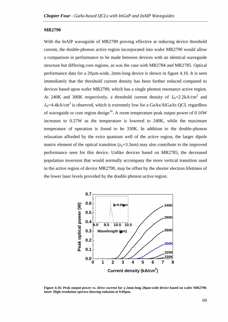
Chapter Four - GaAs-based QCLs with InGaP and InAlP Waveguides
69
MR2790
With the InAlP waveguide of MR2789 proving effective at reducing device threshold
current, the double-phonon active region incorporated into wafer MR2790 would allow
a comparison in performance to be made between devices with an identical waveguide
structure but differing core regions, as was the case with MR2784 and MR2785. Optical
performance data for a 20µm-wide, 2mm-long device is shown in figure 4.16. It is seen
immediately that the threshold current density has been further reduced compared to
devices based upon wafer MR2789, which has a single phonon resonance active region.
At 240K and 300K respectively, a threshold current density of Jth=2.2kA/cm2 and
Jth=4.4kA/cm2 is observed, which is extremely low for a GaAs/AlGaAs QCL regardless
of waveguide or core region design16
. A room temperature peak output power of 0.16W
increases to 0.57W as the temperature is lowered to 240K, while the maximum
temperature of operation is found to be 330K. In addition to the double-phonon
relaxation afforded by the extra quantum well of the active region, the larger dipole
matrix element of the optical transition (zij=3.3nm) may also contribute to the improved
performance seen for this device. Unlike devices based on MR2785, the decreased
population inversion that would normally accompany the more vertical transition used
in the active region of device MR2790, may be offset by the shorter electron lifetimes of
the lower laser levels provided by the double phonon active region.
0 1 2 3 4 5 6 7 80.0
0.1
0.2
0.3
0.4
0.5
0.6
0.7
9.0 9.5 10.0 10.5
Pe
ak
op
tic
al
po
we
r (W
)
Current density (kA/cm2)
240K
300K
260K
280K
320K
330K
Wavelength (m)
=9.69m
Figure 4.16: Peak output power vs. drive current for a 2mm-long 20µm-wide device based on wafer MR2790.
Inset: High-resolution spectra showing emission at 9.69µm.

Chapter Four - GaAs-based QCLs with InGaP and InAlP Waveguides
70
A device with a 3mm cavity length displayed threshold current densities of
Jth=2.1kA/cm2 at 240K and Jth=4.0kA/cm
2 at 300K. These threshold currents observed
for sample MR2790 represent the lowest reported to-date for a GaAs-based QCL, and
enhance the prospects of eventual room-temperature CW operation.
240 260 280 300 320 340
2
3
4
5
6
7
Jth
(k
A/c
m2)
Temperature (K)
T0=85K
Figure 4.17: Threshold current density vs. operating temperature for a 2mm-long, 20µm-wide device based on
wafer MR2790, with corresponding characteristic temerature, T0= 85K.
The Jth vs. T fit for the 2mm device yields T0=85±9K (figure 4.17), while the
waveguide losses, αw for wafer MR2790 were estimated from a linear fit of the
threshold current density versus reciprocal cavity length data as outlined by equations
3.6 and 3.7 in chapter three. Figure 4.18 shows data for a series of devices of length
1mm, 2mm and 3mm, which results in a calculated waveguide loss of αw=7.9±1.8cm-1
at 240K and αw=9.6±1.2cm-1
at room temperature. The inconsistency between the
measured waveguide loss at 300K, and the theoretical value estimated for this structure
from the optical mode profile (see table 4.1) could be due to variations in the doping of
the wafer layers or the parameters used in the calculation being generally applicable to
lower temperatures. The data presented in figure 4.18 also allows the calculation of the
modal gain coefficient gΓ, i.e. the gain coefficient g, multiplied by the waveguide
confinement factor Γ (see section 3.4.4). The value of Γ for the waveguide structure of
MR2790 at a wavelength of λ=9.69µm was calculated to be Γ=0.78, resulting in an

Chapter Four - GaAs-based QCLs with InGaP and InAlP Waveguides
71
estimate of g=7.7±1.2cmkA-1
and g=4.4±0.4cmkA-1
at 240K and 300K respectively for
this sample. The peak material gain at threshold Gp, can also be calculated for these
devices from the relationship Gp=gJth (see equation 3.4), resulting in Gp=17±3cm-1
and
Gp=16±3cm-1
for the 2mm and 3mm devices respectively at 240K, while at 300K
Gp=19±3cm-1
and Gp=18±2cm-1
for 2mm and 3mm lasers.
2 3 4 5 6 7 8 9 10 111
2
3
4
5
6
7 240 K
w = 7.9cm
-1, g = 6.0cmkA
-1
300 K
w = 9.6cm
-1, g = 3.5cmkA
-1
Jth
(kA
/cm
2)
1/L (cm-1
)
Figure 4.18: Threshold current density vs. reciprocal cavity length for 1, 2 and 3mm-long devices at an
operating temperature of 240K and 300K. The linear fit yields values for the waveguide loss αw for devices
fabricated from wafer MR2790.
The measured gain coefficients can be compared to those determined for other GaAs-
based devices operating at λ~9µm. Barbieri et al17
and Sirtori et al7 studied devices with
a three-well GaAs/Al0.33Ga0.67As active region utilising a diagonal electronic transition,
and reported coefficients of g=6.7cmkA-1
and g=8.7cmkA-1
respectively. A second
study by Sirtori et al9 observed an increased gain coefficient of g=15.8cmkA
-1 for a
similar GaAs/Al0.33Ga0.67As device with a highly-doped GaAs waveguide. In all these
cases the optical confinement afforded by the device waveguides (either Al0.9Ga0.1As or
GaAs) was considerably lower than the Γ=0.78 calculated for MR2790, with
confinement factors ranging between 0.31 ≤ Γ ≤ 0.42. Higher optical confinement
would have naturally lead to an increased gain coefficient. Reported waveguide losses
were also correspondingly larger than those calculated here, with αw≈20cm-1
being
measured in all cases. The gain coefficient measured for MR2790 is consistent with

Chapter Four - GaAs-based QCLs with InGaP and InAlP Waveguides
72
those measured in references [7] and [17], but is approximately half that reported by
Sirtori et al in reference [9]. It should be noted however, that the temperature at which g
was determined was 77K in the case of the Sirtori studies and 200K for Barbieri et al,
in comparison to 240K and 300K for sample MR2790.
Since the optical confinement afforded by the InAlP waveguide of MR2790 is already
considerably larger than that provided by either Al0.9Ga0.1As or highly-doped GaAs
waveguides (with correspondingly lower losses), the results of Sirtori et al suggest that
there may be scope for increasing the gain of the GaAs devices presented in this
chapter through alterations to the device active region. For example, the fact that there
were observed reductions in performance when moving from the diagonal transition of
MR2784 to the more vertical design of MR2785, means it may be possible to reduce
the spatial overlap of the optical transition of MR2790 and still experience the benefit
of increased gain due to the larger population inversion between upper and lower states
that would result (see equation 2.4). As shown by equation 3.4, any increase in g that
could be achieved would lead to further reductions in the threshold current density of
devices (assuming waveguide losses remain the same), and would enhance the prospect
of operation at high duty cycles and in the CW regime.
4.6.3 Current -Voltage Characteristics
In addition to the optical characteristics of devices fabricated from each wafer design,
electrical performance, in the form of voltage-current curves were also measured for
each laser. Shown in figure 4.19 is the I-V data for 3mm-long, 20µm-wide devices at
liquid nitrogen (~77K) and room temperature. Upon inspection, a marked difference
between the electrical performance of devices utilising either InGaP or InAlP
waveguides is immediately apparent. Devices with the InGaP waveguide structure show
I-V characteristics which are fairly typical for a GaAs-based QCL at both room and low
temperature, where voltages approach ~13.5V and ~16V at 293K and 77K respectively.
This is consistent with the expected operating voltage Vop, which can be estimated
simply by multiplying the total transition energy of the device active region by the
number of periods within in the core i.e.:

Chapter Four - GaAs-based QCLs with InGaP and InAlP Waveguides
73
[ ( )]
(4.1)
where NP is the number of core region periods, Eλ is the emission energy in eV, and ΔEV
is the voltage defect, i.e. the energy separation between the lower laser level of one
active region and the upper laser level of the next active region18
.
For devices containing InAlP waveguides however, the situation is very different.
Operating voltages are dramatically increased compared to InGaP lasers, with voltages
reaching in excess of 55V for devices from both wafers MR2789 and MR2790 at 77K.
At room temperature, voltages are approximately double that of InGaP devices where
they approach ~30V and 25V for MR2789 and MR2790 respectively. These voltages
invariably lead to an excessive amount of heating within devices, and thus contributed
to a high incidence of device failure.
0 1 2 3 4 50
10
20
30
40
50
60
MR2784
MR2785
MR2789
MR2790
Vo
ltag
e (
V)
Current Density (kA/cm2)
4.19: I-V characteristics for devices MR2784
0 1 2 3 4 50
5
10
15
20
25
30
35
MR2784
MR2785
MR2789
MR2790
Vo
ltag
e (
V)
Current Density (kA/cm2)
Figure 4.19: I-V characteristics for devices MR2784 through MR2790 at (a) 80K and (b) room-temperature.
The large operating voltages observed imply that either the InAlP layer itself represents
a fundamental obstacle to the current flow in these devices, or that the transitional layers
inserted at the GaAs/InAlP interfaces were not sufficiently optimised for efficient
electron transport across the interfaces. In order to test the latter suggestion, a wafer was
grown in which the transitional layer was modified by excluding the
(a) (b)

Chapter Four - GaAs-based QCLs with InGaP and InAlP Waveguides
74
In0.49(Ga0.5Al0.5)0.51P section and replacing it with InGaP, resulting in a single layer of
In0.49Ga0.51P 42nm in thickness. The remainder of the structure was identical to
MR2790, including the double-phonon active region. A comparison of the I-V
characteristics for a 2mm-long, 20µm-wide device fabricated from wafer MR2790 and a
2mm, 30µm-wide laser fabricated from the modified wafer can be seen in figure 4.20.
0 1 2 3 4 5 6 7 80
10
20
30
40
50
60
70
80 MR2790:
25/16nm InGaP/InGaAlP
transitional layer
Modified design:
42nm InGaP
transitional layer
Vo
lta
ge
(V
)
Current density (kA/cm2)
Figure 4.20: Room-temperature I-V characteristics comparing the electrical performance of device MR2790
with that of a device with a modified transitional layer (TL) at the GaAs/InAlP interface. The modification
consists of removing the InGaAlP part of the TL in MR2790 and replacing it with InGaP, resulting in a TL
comprising of 42nm of InGaP.
It is apparent that the removal of In0.49(Ga0.5Al0.5)0.51P from the transitional layer has an
adverse affect on the operating voltage of this device, where at threshold (~4.4kA/cm2)
a voltage of 53V is observed, rising to over 70V at 6.7kA/cm2. This is approximately
double the voltage observed for MR2790 which includes In0.49(Ga0.5Al0.5)0.51P in the
transitional layer at the GaAs/InAlP interface. It is not possible to state how optimised
the previous structure was in terms of device operating voltage, but the result does
suggest that at the least there is considerable scope for further tailoring of the layers at
the GaAs/InAlP interfaces, along with the possibility of reducing operating voltages.

Chapter Four - GaAs-based QCLs with InGaP and InAlP Waveguides
75
Despite the large operating voltages, the optical performance of lasers fabricated from
the modified wafer was found to be largely comparable to that of MR2790. The
characteristic temperature for the modified device was found to be T0=82K - slightly
lower than the 85K of MR2790 - while higher threshold current densities of 2.7kA/cm2
and 5.4kA/cm2 were observed at 240K and 300K respectively. Peak output powers of
0.72W at 240K and 0.24W at 300K were also measured, a slight increase to those
recorded for MR2790.
Shown below in table 4.3 is a summary of the key performance parameters for devices
fabricated from each wafer:
Sample λ300K
(µm)
Jth
(kA/cm2)
Peak Power
(W)
Vmax
(V)
T0
(K)
Tmax
(K)
MR2784
2mm 9.08
4.4 (240K)
8.2 (300K)
1.58 (240K)
0.56 (300K)
13.5 (300K)
16 (80K) 95 340
MR2785
3mm 8.77
4.7 (240K)
8.6 (300K)
0.77 (240K)
0.20 (300K)
13.5 (300K)
16 (80K) 96 320
MR2789
3mm 8.68
3.8 (240K)
7.3 (300K)
0.83 (240K)
0.20 (300K)
30 (300K)
57 (80K) 93 320
MR2790
2mm 9.69
2.2 (240K)
4.4 (300K)
0.57 (240K)
0.16 (300K)
25 (300K)
57 (80K) 85 330
Table 4.3: Performance summary of key characteristics for devices MR2784 through MR2790.

Chapter Four - GaAs-based QCLs with InGaP and InAlP Waveguides
76
4.7 Conclusions
This chapter has presented the optical and electrical characteristics of several GaAs-
based QCLs each with differing designs, in order to ascertain the performance benefits
(or otherwise) of each design strategy. It has been shown – in the case of QCLs utilising
InGaP waveguides – how an increase in the number of active region periods may
beneficially affect the interaction of the optical mode with the laser core and lead to an
increase in device output power. It is also seen how in some cases, altering the active
region to change the spatial characteristics of the optical transitions - in this case from
the diagonal transition of MR2784 to the more vertical of MR2785 - can have an
adverse effect on laser performance if the correct balance is not found between the
increased dipole matrix element and the reduced population inversion that results. The
performance reductions that were observed for sample MR2785 however, can be
mitigated by the substitution of a waveguide material that has the potential for greater
optical confinement and lower optical losses than that offered by InGaP. The
enhancements in performance observed for MR2789 can be attributed to the
introduction of the InAlP waveguide since the design is otherwise identical to MR2785.
The benefit of a double-phonon active region has also been demonstrated, with
threshold current densities as low as 2kA/cm2 and 4kA/cm
2 having been observed at
240K and 300K respectively for MR2790 – the lowest Jth for a GaAs-based QCL at
these temperatures reported to-date. Other performance characteristics such as peak
output power are at least comparable with other GaAs-based devices, confirming the
potential for further performance enhancements of QCLs that incorporate InAlP as the
waveguide material.
Despite these successes, it has also been shown that InAlP can introduce characteristics
detrimental to device performance. The high operating voltages observed in lasers with
InAlP waveguides are a major cause of device failure, and will almost certainly inhibit
any attempt to run devices at higher duty cycles. Optimisation of the transitional layers
at the GaAs/InAlP interfaces is one strategy that may reduce these voltages, and this
approach will form the main focus of the next chapter. If the low threshold current
densities that are characteristic of devices with InAlP waveguides, can be combined
with the lower operating voltages and improved characteristic temperatures associated
with devices with InGaP waveguides, it may enhance the prospects for CW operation of
Chapter Four - GaAs-based QCLs with InGaP and InAlP Waveguides
77
GaAs-based QCLs at higher temperatures than have previously been achieved – 150K at
the time of writing11
.

Chapter Four - GaAs-based QCLs with InGaP and InAlP Waveguides
78
1. L. R. Wilson, P. T. Keightley, J. W. Cockburn, J. P. Duck, M. S. Skolnick, J. C. Clark, G. Hill, M.
Moran and R. Grey, Spectroscopic determination of the electron distribution in a quantum cascade
structure, Applied Physics Letters, 75, 2079-2081, (1999).
2. J. S. Roberts, R. P. Green, L. R. Wilson, E. A. Zibik, D. G. Revin, J. W. Cockburn and R. J. Airey,
Quantum cascade lasers grown by metalorganic vapor phase epitaxy, Applied Physics Letters, 82, 4221-
4223, (2003).
3. R. P. Green, L. R. Wilson, D. A. Carder, J. W. Cockburn, M. Hopkinson, M. J. Steer, R. J. Airey
and G. Hill, Room temperature GaAs-based quantum cascade laser with GaInP waveguide cladding,
Electronics Letters, 38, 1539-1541, (2002).
4. L. R. Wilson, P. T. Keightley, J. W. Cockburn, J. P. Duck, M. S. Skolnick, J. C. Clark, G. Hill, M.
Moran and R. Grey, Mid-infrared spectroscopic studies and lasing in GaAs-AlGaAs quantum cascade
devices, Physica E, 7, 713-717, (2000).
5. L. R. Wilson, P. T. Keightley, J. W. Cockburn, M. S. Skolnick, J. C. Clark, R. Grey and G. Hill,
Controlling the performance of GaAs-AlGaAs quantum-cascade lasers via barrier height modifications,
Applied Physics Letters, 76, 801-803, (2000).
6. A. B. Krysa, D. G. Revin, J. P. Commin, C. N. Atkins, K. Kennedy, Y. Qiu, T. Walther and J. W.
Cockburn, Room-Temperature GaAs/AlGaAs Quantum Cascade Lasers Grown by Metal-Organic Vapor
Phase Epitaxy, Ieee Photonics Technology Letters, 23, 774-776, (2011).
7. C. Sirtori, P. Kruck, S. Barbieri, P. Collot, J. Nagle, M. Beck, J. Faist and U. Oesterle,
GaAs/AlxGa1-xAs quantum cascade lasers, Applied Physics Letters, 73, 3486-3488, (1998).
8. C. Sirtori, S. Barbieri, P. Kruck, V. Piazza, M. Beck, J. Faist, U. Oesterle, P. Collot and J. Nagle,
Influence of DX centers on the performance of unipolar semiconductor lasers based on GaAs-AlxGa1-xAs,
IEEE Photonics Technology Letters, 11, 1090-1092, (1999).
9. C. Sirtori, P. Kruck, S. Barbieri, H. Page, J. Nagle, M. Beck, J. Faist and U. Oesterle, Low-loss Al-
free waveguides for unipolar semiconductor lasers, Applied Physics Letters, 75, 3911-3913, (1999).
10. H. Page, S. Dhillon, M. Calligaro, V. Ortiz and C. Sirtori, Optimised device processing for
continuous-wave operation in GaAs-based quantum cascade lasers, Electronics Letters, 39, 1053-1055,
(2003).
11. H. Page, S. Dhillon, M. Calligaro, C. Becker, V. Ortiz and C. Sirtori, Improved CW operation of
GaAs-Based QC lasers: T-max=150 K, Ieee Journal of Quantum Electronics, 40, 665-672, (2004).
12. H. Page, C. Becker, A. Robertson, G. Glastre, V. Ortiz and C. Sirtori, 300 K operation of a GaAs-
based quantum-cascade laser at ~ 9m, Applied Physics Letters, 78, 3529-3531, (2001).
13. S. Adachi, Properties of Semiconductor Alloys, (Wiley, 2009).
Chapter Four - GaAs-based QCLs with InGaP and InAlP Waveguides
79
14. Q. Yang, R. Losch, W. Bronner, S. Hugger, F. Fuchs, R. Aidam and J. Wagner, High-peak-power
strain-compensated GaInAs/AlInAs quantum cascade lasers (λ~4.6µm) based on a slightly diagonal
active region design, Applied Physics Letters, 93, 251110, (2008).
15. M. O. Watanabe and Y. Ohba, Interface properties for GaAs/InGaAlP heterojunctions by the
capacitance-voltage profiling technique, Applied Physics Letters, 50, 906-908, (1987).
16. C. N. Atkins, A. B. Krysa, D. G. Revin, K. Kennedy, J. P. Commin and J. W. Cockburn, Low
threshold room temperature GaAs/AlGaAs quantum cascade laser with InAlP waveguide, Electronics
Letters, 47, 1193-1194, (2011).
17. S. Barbieri, C. Sirtori, H. Page, M. Beck, J. Faist and J. Nagle, Gain measurements on GaAs-based
quantum cascade lasers using a two-section cavity technique, IEEE Journal of Quantum Electronics, 36,
736-741, (2000).
18. R. Maulini, A. Lyakh, A. Tsekoun and C. K. N. Patel, λ~7.1µm quantum cascade lasers with 19%
wall-plug efficiency at room temperature, Optics Express, 19, 17203-17211, (2011).

80
Chapter Five
Design Optimisation for GaAs-
based QCLs with InAlP
Waveguides
5.1 Introduction
Chapter four included a discussion of the excessive operating voltages measured for
QCLs incorporating InAlP waveguides, and how these voltages led to a high incidence
of device failure - partly negating the performance gains otherwise observed. It was
suggested that the source of these high voltages was the comparatively large
conduction-band offset at the GaAs/InAlP interfaces within the device structure, which
would inhibit electron flow through devices at these points. This challenge had, to some
extent, been anticipated when designing the QCLs presented in chapter four, and led to
the introduction of the InGaP/InGaAlP transitional layers between the GaAs/InAlP
interfaces. For the next iteration of wafer design it was decided that a more
sophisticated approach to managing the GaAs/InAlP interfaces should be taken in an
attempt to further reduce operating voltages.
This chapter will consist of a discussion of two new designs for the transitional layers
that bridge the GaAs/InAlP interfaces within a series of four GaAs-based QCL wafers
with InAlP waveguides. These new designs increase the complexity of the layer
structure at the GaAs/InAlP interfaces and are detailed in section 5.2. Two of the wafers
reproduce the cladding layer and core-region structure of wafer MR2790 from chapter
four, but incorporate one or other of the new transitional layers in order to observe their
effect on device operating voltage. The remaining two wafers also include one of the
transitional layers, but have a modified core region which includes several high-

Chapter Five - Design Optimisation for GaAs-based QCLs with InAlP Waveguides
81
aluminium Al0.75Ga0.25As barriers in the injector region, the addition of which represent
an attempt to reduce the probability of electron escape from the upper laser level into
the electronic states that exist above the injector region barriers. This non-radiative
electron pathway can act to decrease population inversion within the device active
region and thus compromise device performance - especially at higher temperatures.
This strategy of selectively including high-Al fraction barriers within the QCL core
region has been implemented in several previous studies1-3
. For example, Yang and co-
workers4 replaced the standard AlInAs exit barrier of an InGaAs/AlInAs QCL active
region with an AlAs ‘blocking barrier’ in order to increase the conduction band offset
relative to the preceding quantum well. Consequent improvements in device
performance included a 30K increase in maximum operating temperature and threefold
increase in output power, both of which were attributed to the increased confinement of
electrons in the upper energy level and subsequent reduction of non-radiative tunnelling
into continuum states. As well as the addition of high-Al barriers, various changes to
well and barrier widths throughout the core region have been made. The full design
details of each wafer are given in the next section. Following the discussion of wafer
design, the electrical and optical characteristics of devices fabricated from each wafer
are presented, and the effects on device performance produced by the various different
design strategies will be compared.
5.2 Wafer Design
MR3066
The layer sequence for wafer MR3066 (shown schematically in figure 5.1) closely
follows that of MR2790 outlined in chapter four, with the exception of the modified
transitional layers that now occupy the GaAs/InAlP interfaces. Rather than the
InGaP/InGaAlP layer that was used at each interface in wafers MR2789 and MR2790,
the layer sequence is now dependent upon which GaAs/InAlP interface is being
considered. In the case of MR3066, there are four relevant interfaces, which starting
from the GaAs substrate and working in the direction of growth can be numbered 1
through 4, and the transitional layer associated with each termed TL1, TL2, TL3 and
TL4 as shown in figure 5.1. TL1 comprises of 40nm InGaP (N=1x10¹⁸
cm-3
) followed by

Chapter Five - Design Optimisation for GaAs-based QCLs with InAlP Waveguides
82
60nm InAlP (graded N=1x10¹⁸
→ 1x10¹⁷
cm-3
), while TL3 consists of a single 40nm
thick layer of In0.49Ga0.51P (N=1x10¹⁷
cm-3
). TL2 and TL4 are formed by a superlattice of
alternating InGaP and InAlP layers, the thicknesses of which are graded so that the
width of the InGaP layers increases in the growth direction, whilst the InAlP decreases
in width in the same direction.
Starting from the InAlP waveguide and working in the direction of growth, the structure
of the superlattice TL2 and TL4, also shown schematically in figure 5.1, is as follows:
0.6/4.0/0.8/4.0/1.0/3.5/1.3/3.5/1.5/3.0/2/2.0/2.5/1.5/3/1.5/4/1.5/5/1.5/6/1.5/10/1.5/20/10/
40, where thicknesses are in nm, normal font represents In0.49Ga0.51P layers, and bold
font In0.47Al0.53P layers. For TL2 the penultimate 10nm InGaP layer at the end of the
sequence (shown in red italicised font) is omitted and all layers are Si-doped to
N=1x10¹⁷
cm-3
, while for TL4 the final two layers are both doped to N=1x10¹⁸
cm-3
.
The complete layer sequence for wafer MR3066, starting from the GaAs substrate
(N=3x10¹⁸
cm-3
) and including transitional layers is as follows: 1µm GaAs bottom
cladding (N=3x10¹⁸
cm-3
), TL1, 3µm In0.47Al0.53P waveguide layer (N=1x10¹⁷
cm-3
),
superlattice TL2, 0.2µm GaAs spacer layer (N=5x10¹⁶
cm-3
), GaAs/Al0.45Ga0.55As core
region (55 periods, 3.041µm), 0.2µm GaAs spacer, TL3, 3µm In0.47Al0.53P waveguide,
superlattice TL4 and finally 1µm GaAs top cladding. The core region structure is a copy
of the double-phonon design used in wafer MR2790, details of which are given in
section 4.5 of chapter four along with the corresponding conduction band profile (figure
4.7).

Chapter Five - Design Optimisation for GaAs-based QCLs with InAlP Waveguides
83
Figure 5.1: Schematic illustration of the layer structure for wafers MR3066 and MR3069, including
transitional layers at the GaAs/InAlP interfaces.
MR3069
Wafer MR3069 replicates the layer sequence of MR3066, except for the inclusion of
three high-aluminium Al0.75Ga0.25As barriers in the injector region. As mentioned in the
introduction above, these barriers represent an attempt to increase the high-temperature
performance of devices by reducing the probability of electron escape from the upper
laser level (Eu) into the higher-lying states above the injector region. For the
composition x=0.75, Al0.75Ga0.25As barriers provide an increase in conduction band
offset of ~0.32eV relative to the GaAs/Al0.45Ga0.55As offset in the remainder of the core
region, while still remaining lattice matched with the GaAs quantum wells. Beginning
from the injection barrier, this new core region design has the following structure:
Chapter Five - Design Optimisation for GaAs-based QCLs with InAlP Waveguides
84
4.2/2.1/1.0/5.0/1.0/4.9/1.0/4.6/1.0/1.0/3.9/1.6/3.7/1.6/3.5/1.8/3.2/2.1/2.9/2.7/2.9,
where normal font represents the GaAs wells, bold font the Al0.45Ga0.55As barriers and
red italicised font the Al0.75Ga0.25As barriers. Underlined layers are Si-doped to
N=4x10¹⁷
cm-3
.
In addition to the Al0.75Ga0.25As barriers in the injector region, the core has undergone
several other changes including a widening of the first active region quantum well and a
narrowing of the succeeding three wells that constitute the remainder of the active
region. The barriers associated with these wells have been correspondingly widened.
The injector region has seen similar alterations to well and barrier thicknesses, with the
majority of the quantum wells being increased in thickness, while barriers preceding the
doped region of the injector have been slightly narrowed. In common with wafer
MR3066, MR3069 contains the graded superlattice transitional layer detailed above.
The core region conduction band profile, showing the moduli squared of the electronic
wavefunctions associated with both the laser transition and the injector miniband is
given in figure 5.2, where the increased conduction band offset provided by the
Al0.75Ga0.25As barriers is clearly illustrated. The alterations to the active region have
also resulted in a reduction in dipole matrix element for the optical transition of
zij=2.8nm, compared to zij=3.3nm for MR3066.

Chapter Five - Design Optimisation for GaAs-based QCLs with InAlP Waveguides
85
0 20 40 60 80
1.0
1.2
1.4
1.6
1.8
2.0
2.2
valley
valleyE
l
Ei E
u
En
erg
y (
eV
)
Distance (nm)
Eu
Figure 5.2: Γ-point conduction band profile for the core region of MR3069 and MR3082 under a bias of
48kV/cm2. Also shown for reference in the X-valley profile (see discussion in section 5.3.2). The Γ-profile
includes the moduli-squared of the electronic wavefunctions associated with the optical transition (shown in
red), and the injector level (blue). The effect of the high-Al barriers on the conduction band offset is clearly
illustrated.
MR3076
The layer structure and core region design of wafer MR3076 is a copy of
MR3066, with the exception of the transitional layers 1 → 4 that appear the
GaAs/InAlP interfaces. The graded superlattice design that constituted TL2 and TL4 in
wafers MR3066 and MR3069, has been replaced by a ‘stepped’ transitional layer
containing three 20nm thick sub-layers of In0.49(Ga1-xAlx)0.51P in which the Al-fraction
is sequentially reduced from 0.7 ≤ x ≤ 0.3 in the direction of growth, and a final layer
consisting of 40nm of In0.49Ga0.51P. The full transitional layer sequence is as follows:
In0.49(Ga0.3Al0.7)0.51P/In0.49(Ga0.5Al0.5)0.51P/In0.49(Ga0.7Al0.3)0.51P/In0.49Ga0.51P,
with layers doped to N=1x10¹⁷
cm-3
at TL2 and N=1x10¹⁸
cm-3
at TL4. Transitional layer
1 comprises of 40nm of In0.49Ga0.51P (N=1x10¹⁸
cm-3
), 20nm of In0.49(Ga0.5Al0.5)0.51P
(N=1x10¹⁸
cm-3
) and 60nm of In0.47Al0.53P (graded N=1x10¹⁸
cm-3
→ N=1x10¹⁷
cm-3).
Finally, transitional layer 3 is formed by a 40nm layer of In0.49Ga0.51P followed by 20nm
of In0.49(Ga0.5Al0.5)0.51P (both N=1x10¹⁷
cm-3
). A schematic of the layer structure for
MR3076 and its associated TLs are shown in figure 5.3.

Chapter Five - Design Optimisation for GaAs-based QCLs with InAlP Waveguides
86
Figure 5.3: Schematic illustration of the layer structure for wafers MR3076 and MR3082, including
transitional layers.
MR3082
Finally, wafer MR3082 reproduces the layer structure and transitional layers of
MR3076 (see figure 5.3), while incorporating the high-aluminium core region used in
MR3069, details of which can be found in the relevant section above.
In common with the previous series of wafers presented in chapter four, all wafers
described above were grown using MOVPE on GaAs substrates with a 10° miscut
toward the (111) plane. The growth conditions were identical throughout the run and are
detailed in section 4.5 of chapter 4.

Chapter Five - Design Optimisation for GaAs-based QCLs with InAlP Waveguides
87
Design Summary
Table 5.1 provides a summary of the key design features of each wafer for comparison:
Wafer Active Region
Design
Transitional
Layer
Waveguide
Material
Γ (%) /
αw (cm-1)
MR3066
Double-phonon
‘Vertical’
transition
Superlattice
InGaP/InAlP InAlP 81 / 4.8
MR3069
Double-phonon
Diagonal transition
75% Al Barriers
Superlattice
InGaP/InAlP InAlP 81 / 4.8
MR3076
Double-phonon
‘Vertical’
transition
Stepped
InGaP/InGaAlP InAlP 81 / 4.8
MR3082
Double-phonon
Diagonal transition
75% Al Barriers
Stepped
InGaP/InGaAlP InAlP 81 / 4.8
Table 5.1: Summary outlining the main design features of each wafer.
5.3 Device Performance
After processing, wafers were cleaved into a series of 3mm-long devices with ridge
widths of either 16µm or 21µm, and mounted onto T05 headers for characterisation. As
with the previous series of devices presented in chapter four, all measurements were
made in pulsed mode with a pulse width of 50ns and repetition rate of 5kHz.

Chapter Five - Design Optimisation for GaAs-based QCLs with InAlP Waveguides
88
5.3.1 Electrical Characteristics
Inclusion of the superlattice and stepped transitional layers in the new wafer designs
represented an attempt to reduce the excessive operating voltages observed in the
previous set of QCLs with InAlP waveguides. A series of room and low-temperature
current-voltage measurements are shown in figure 5.4, contrasting the operating
voltages of devices incorporating the superlattice and stepped transitional layers. Data
for device MR2790 (from the previous series of lasers) is also presented for comparison.
Figure 5.4: I-V characteristics for (a) devices MR3066 and MR3076 and (b) MR3069 and MR3082, at 80K and
room-temperature. Shown for comparison in blue is the room-temperature I-V for device MR2790 featured in
chapter four.
Figure 5.4 (a) compares the I-V characteristics for a set of 3mm-long, 16um-wide
devices fabricated from wafers MR3066 (superlattice TL) and MR3076 (stepped TL)
which, besides the differing TLs, have an identical layer structure and core region. It
can be seen that at room temperature, only a small difference in operating voltage is
observed between the two devices over the entire current range, where the voltage for
MR3076 begins to diverge from MR3066 at approximately 5kA/cm2. At threshold, both
devices run at ~22V, while at maximum current density (Jmax~9kA/cm2) a difference of
only 1V exists between the two - 29V and 30V for MR3066 and MR3076 respectively.
At liquid nitrogen temperatures, the difference in operating voltage becomes slightly
more pronounced, with MR3066 and MR3076 running at ~34V and ~36.5V
respectively at maximum drive current.
(a)
0 1 2 3 4 5 6 7 8 9 100
5
10
15
20
25
30
35
40
MR3066 RT
MR3076 RT
MR3066 80K
MR3076 80K
MR2790 RT
Vo
lta
ge (
V)
Current density (kA/cm2)
(a)
0 1 2 3 4 5 6 7 8 9 100
5
10
15
20
25
30
35
40
45
MR3069 RT
MR3082 RT
MR3069 80K
MR3082 80K
MR2790 RT
Vo
lta
ge (
V)
Current density (kA/cm2)
(b)

Chapter Five - Design Optimisation for GaAs-based QCLs with InAlP Waveguides
89
In comparison to device MR2790 (shown in blue in figure 5.4), these voltages represent
a reduction in operating voltage at room temperature of ~12V (at a comparable current
of 7kA/cm2), while at 80K reductions are even more marked. As shown in chapter four
(figure 4.19), a maximum low temperature voltage of Vmax~57V at 2.8kA/cm2 was
observed for MR2790, resulting in a significant incidence of device failure. By
comparison, a Vmax of ~35V at the same low temperature but much higher current
density (~9kA/cm2) for MR3066 and MR3076 represents a significant reduction. These
voltages are still high however, when contrasted with devices MR2784 and MR2785
which incorporated InGaP waveguides and operated at ~12-15V at room and low-
temperature.
The small voltage differences observed between devices with the superlattice and
stepped TLs seen above, are somewhat enhanced when measuring lasers based upon
wafers MR3069 and MR3082 (superlattice and stepped TLs respectively), which
include Al0.75Ga0.55As barriers in the core region. As seen in figure 5.4 (b), the room-
temperature operating voltage of MR3082 shows a greater divergence from MR3069
than was observed between MR3066 and MR30776, and results in a disparity of ~4V at
6kA/cm2 (the maximum drive current for device MR3082). At this point voltages of
30V and ~26V are measured for MR2782 and MR3069 respectively. The maximum
voltage observed for device MR3069 is Vmax~34V at 9kA/cm2, larger than either
MR3066 or MR3076 (29V and 30V respectively). Voltage at threshold is 26V for both
devices, despite MR3082 having a lower threshold current density (~5kA/cm2 compared
to ~6kA/cm2). At 80K device MR3069 is observed to run at 42V at maximum current
(9kA/cm2), compared to ~40V for MR3082 (maximum current 5kA/cm
2).
Contrasting the electrical characteristics of each device allows for certain behaviours
and trends to be discerned. Firstly, at room temperature there is very little difference in
the operating voltages of devices with Al0.45Ga0.55As barriers that contain either the
superlattice or stepped TLs (MR3066 and MR3076), over their entire working current
range. At 80K a more obvious difference in voltage is observed between the two
devices, which is more pronounced at larger currents. This disparity however, remains a
relatively small 2.5V at maximum current. Any further increase in this voltage
difference at higher currents is unlikely to affect the comparison since this would
exceed the rollover in power output of both devices. A greater difference in room-
temperature operating voltage is observed when comparing devices with Al0.75Ga0.25As

Chapter Five - Design Optimisation for GaAs-based QCLs with InAlP Waveguides
90
barriers, i.e. MR3069 (superlattice TL) and MR3082 (stepped TL), which at its largest
reaches 3.5V at a current density of J=6kA/cm2.
It is clear that a more marked difference in operating voltage exists if comparing devices
with the same transitional layer, but either Al0.45Ga0.55As or the higher-aluminium
Al0.75Ga0.25As barriers in the core region – i.e. MR3066 vs. MR3069 or MR3076 vs.
MR3082. The largest observed voltage difference observed is ~5V at J=9kA/cm2
between MR3066 and MR3069, although by extrapolating the voltage for MR3082 to a
drive current of J=9kA/cm2 a difference of ~10V can be estimated between this device
and MR3076. If device MR3066 (superlattice TL and Al0.45Ga0.55As barriers) is taken as
the starting point for comparison, the addition of the stepped TL (MR3076) appears to
introduce an additional component to the voltage drop of within the structure - a trend
which is replicated between MR3069 and MR3082. An additional unexpected voltage
drop then appears for the lasers with the Al0.75Ga0.25As barriers in the core region,
resulting in MR3082 (stepped TL and Al0.75Ga0.25As barriers) running at the highest
voltage. It is unclear at present why devices with high-Al barriers in the injector region
should display this additional voltage. It is possible that variations in the MOVPE
growth conditions have led to fluctuations in the doping, which would be particularly
sensitive near the transitional layer interfaces and could affect the voltage drop across
the device.
5.3.2 Optical Characteristics
MR3066
As discussed above, wafer MR3066 copies the double-phonon active region design of
MR2790, while incorporating the new superlattice transitional layer. Figure 5.5 shows
the light power vs. current data for a 3mm-long, 21µm-wide device, while the inset
contains a high-resolution (0.25cm-1
) room temperature FTIR spectra showing emission
at λ=10.43µm. The threshold current density for this device at 240K is 2.9kA/cm2 rising
to 5.4kA/cm2 at 300K, while a narrower 16µm laser demonstrated threshold currents of
3.0kA/cm2 and 5.3kA/cm
2 at 240K and 300K respectively. Peak optical output powers
are found to reduce from a maximum of 0.34W at 240K to 0.08W at 300K, while the
narrower device has a peak power of 0.21W at 240K and 0.08W at 300K.

Chapter Five - Design Optimisation for GaAs-based QCLs with InAlP Waveguides
91
2 3 4 5 6 7 80.00
0.05
0.10
0.15
0.20
0.25
0.30
0.35
0.40
10 11 12
Pe
ak
ou
tpu
t p
ow
er
(W)
Current density (kA/cm2)
240K
260K
280K
300K
310K
320K
Wavelength (m)
=10.43m
Figure 5.5: Peak output power vs. current density for a 3mm-long 21µm-wide device fabricated from wafer
MR3066. Inset: High-resolution (0.25cm-1) FTIR spectra showing emission at 10.43µm.
The temperature range over which devices operate is comparable with the previous
series of GaAs lasers, with the 21µm and 16µm wide devices having maximum
operating temperatures of 320K and 340K respectively. An exponential fit of the
threshold current density versus temperature data for the 21µm device is shown in
figure 5.6, and reveals a characteristic temperature of T0=94±13K, while the 16µm wide
laser exhibited T0=102±18K.

Chapter Five - Design Optimisation for GaAs-based QCLs with InAlP Waveguides
92
240 260 280 300 3202
3
4
5
6
7
8
Jth
(kA
/cm
2)
T (K)
T0=94K
Figure 5.6: Threshold current density vs. operating temperature for a 3mm-long, 21µm-wide device fabricated
from MR3066, yielding a characteristic temperature T0=94K.
Comparing the performance of MR3066 with that of MR2790, it can be seen that the
threshold current density of the former does not reach the low levels of the latter despite
the retention of the InAlP waveguide. Output power is also reduced in comparison to
MR2790. It is possible that the longer emission wavelength observed for device
MR3066 has resulted in an increase in the optical losses associated with the waveguide
structure and caused a subsequent reduction in device performance. A calculation of Γ
and αw for MR3066 at the emission wavelength of λ=10.43µm results in Γ=76% and
αw=7.5cm-1
, which represents a slight reduction in modal overlap compared to MR2790
(Γ=78% at λ=9.69µm) along with an increased waveguide loss (αw=5.7cm-1
).
MR3076
Wafer MR3076 retains the core region and cladding design of MR3066, but replaces the
superlattice transitional layer with the stepped InGaP/InGaAlP design outlined above.
As expected, the emission wavelength of λ=10.40µm (inset to figure 5.7) is almost
identical to that of MR3066. Other performance characteristics are detailed in figures
5.7 and 5.8, and show several variations when compared to devices based on MR3066.

Chapter Five - Design Optimisation for GaAs-based QCLs with InAlP Waveguides
93
A 3mm-long, 16µm-wide device demonstrated a threshold current density of
Jth=2.7kA/cm2 at 240K, while a 21µm device exhibited an almost identical
Jth=2.8kA/cm2. At 300K, the threshold current density rises to 5.1kA/cm
2 and
5.2kA/cm2 for 16µm and 21µm-wide lasers respectively. As was the case for MR3066,
these current densities fail to match the low Jth observed for MR2790; Jth=2.1kA/cm2
and 4.0kA/cm2 at 240K and 300K respectively.
1 2 3 4 5 6 7 8 9 100.00
0.05
0.10
0.15
0.20
0.25
0.30
0.35
10 11 12
Pe
ak
ou
tpu
t p
ow
er
(W)
Current density (kA/cm2)
240K
260K
280K
300K
320K
330K340K
Wavelength (m)
10.40m
Figure 5.7: Peak output power vs. current density for a 3mm-long, 16µm-wide device fabricated from wafer
MR3076. Inset: High-resolution spectra.
Peak optical output powers for the 16µm-wide device were found to be 0.32W at 240K,
falling to 0.13W at 300K, while the wider 21µm laser produced almost identical powers
at these temperatures. As was observed for MR3066, maximum operating temperatures
of 340K and 320K for 16µm and 21µm devices respectively were measured. The
characteristic temperatures of T0=95±16K (figure 5.8) and T0=93±15K for 16µm and
21µm devices respectively are consistent with those measured for MR3066.

Chapter Five - Design Optimisation for GaAs-based QCLs with InAlP Waveguides
94
240 260 280 300 320 3402
3
4
5
6
7
89
Jth
(kA
/cm
2)
T (K)
T0=95K
Figure 5.8: Threshold current density vs. operating temperature for a 3mm-long, 16µm-wide device fabricated
from MR3076, yielding T0=95K.
MR3069
While having the same superlattice transitional layer as MR3066, wafer MR3069
incorporates high-Al Al0.75Ga0.25As barriers in the injector region, along with a
correspondingly modified active region. L-I curves for a 3mm-long, 16m-wide device
are shown in figure 5.9, with values of Jth=3.6kA/cm2
and Jth=6.0kA/cm2 being
measured at 240K and 300K respectively. Almost identical threshold currents are
observed for 21µm-wide devices. A peak output power at 240K of 0.36W represents an
increase of ~0.15W compared to MR3066, while at 300K output powers remain
unchanged at P≈0.09W. The emission wavelength of λ=10.49µm shown in the inset to
figure 5.9 is consistent with that of MR3066, while the maximum temperature of
operation is seen to reduce by 20K and 10K in comparison, for the 16µm and 21µm
devices respectively.

Chapter Five - Design Optimisation for GaAs-based QCLs with InAlP Waveguides
95
3 4 5 6 7 8 9 100.00
0.05
0.10
0.15
0.20
0.25
0.30
0.35
0.40
10 11 12
Peak
ou
tpu
t p
ow
er
(W)
Current density (kA/cm2)
240K
260K
280K
300K
310K320K
Wavelength (m)
=10.49m
Figure 5.9: Peak output power vs. current density for a 3mm-long, 16µm-wide device fabricated from wafer
MR3069. Inset: High-resolution spectra.
Figure 5.10 shows T0 for the same 3mm-long 16µm-wide device from the usual fit of Jth
vs. T. As discussed above, the motivation behind the addition of Al0.75Ga0.25As barriers
within the injector region of MR3069 was the desire to increase the high-temperature
performance of devices. From the Jth vs. T data it is seen that a characteristic
temperature of T0=121±33K is observed for this QCL, which appears to represent an
increase of ~20K in comparison to both MR3066 and MR3076 (containing
Al0.45Ga0.55As barriers). However, due to the large accompanying uncertainty in this
value of T0, this conclusion cannot be stated with any confidence without a larger
sample of device characteristics.

Chapter Five - Design Optimisation for GaAs-based QCLs with InAlP Waveguides
96
240 250 260 270 280 290 300 310 3203
4
5
6
7
8
Jth
(kA
/cm
2)
Temperature (K)
T0=121K
Figure 5.10: Threshold current density vs. operating temperature for a 3mm-long, 16µm-wide device
fabricated from MR3069, yielding T0=121K.
MR3082
Wafer MR3082 replicates the core region design, Al0.75Ga0.25As injector region barriers
and cladding layer structure of MR3069, but replaces the superlattice transitional layer
with the stepped InGaP/InGaAlP TL present in MR3076. Shown in figure 5.11 is the
L-I data and emission spectra for a 16µm-wide device, showing peak emission at
λ=10.57µm - slightly longer than was observed previously for MR3069. Threshold
current densities at lower temperatures are consistent with those of MR3069, with
Jth=3.3kA/cm2 measured at 240K. As can be seen however, the maximum operating
temperature for this device is only slightly above 280K, at which point Jth=5.0kA/cm2.

Chapter Five - Design Optimisation for GaAs-based QCLs with InAlP Waveguides
97
1 2 3 4 5 6 7 80.00
0.05
0.10
0.15
0.20
0.25
0.30
0.35
10 11 12
Peak
ou
tpu
t p
ow
er
(W)
Current density (kA/cm2)
240K
260K
280K290K
220K
200K
Wavelength (m)
10.57m
Figure 5.11: Peak output power vs. current density for a 3mm-long, 16µm-wide device fabricated from wafer
MR3082. Inset: High-resolution spectra.
Low temperature peak output power is found to be 0.14W at 240K, less than half that
typically observed at room temperature for other devices featured in this chapter, while
at 280K output power is substantially lower with approximately 0.02W being measured.
This reduced high-temperature performance is replicated in wider devices, where
powers of ~0.17W and ~0.012W were recorded at 240K and 280K respectively. A
characteristic temperature of T0=99±16K can be extracted from the Jth vs. T data shown
in figure 5.12, while a 21µm-wide device exhibited T0=99±22K.

Chapter Five - Design Optimisation for GaAs-based QCLs with InAlP Waveguides
98
200 220 240 260 280 3002
3
4
5
6
7
Jth
(kA
/cm
2)
Temperature (K)
T0=99K
Figure 5.12: Threshold current density vs. operating temperature for a 3mm-long, 16µm-wide device
fabricated from MR3082, yielding T0=99K.
Table 5.2 contains a summary of the performance characteristics for the set of 3mm-
long, 16µm-wide devices representing each wafer. It can be seen that the emission
wavelengths remain consistent between devices with the same core region design i.e.
MR3066/76 and MR3069/82, as would be expected. It was hoped the addition of
Al0.75Ga0.25As barriers in the core region of devices MR3069 and MR3082 would
improve high-temperature performance by limiting the loss of electrons from the upper
level of the active region to above-barrier continuum states. Enhancements that may
have been expected include an increase in the maximum temperature of laser operation,
a lowering of the threshold current densities at higher temperatures and a concomitant
increase in the device characteristic temperature T0. From the data relating to MR3069
and MR3082 however, the addition of Al0.75Ga0.25As barriers is seen to have a
detrimental effect on these areas of operation. No lowering of Jth is seen at higher
temperatures when compared to MR3066 and MR3076, and at lower temperatures Jth
has increased in comparison to the devices without Al0.75Ga0.25As barriers. Operating
voltages, particularly at 77K also appear to increase with the addition of Al0.75Ga0.25As
barriers to the QCL active region. The maximum temperature of operation has been
reduced by T~20K in the case of MR3069 and T~50K for MR3082 when compared to
devices with Al0.45Ga0.55As barriers. Due to the large uncertainty in T0 measurements, it

Chapter Five - Design Optimisation for GaAs-based QCLs with InAlP Waveguides
99
is also difficult to conclude that characteristic temperatures have been increased with
respect to MR3066 and MR3076. It would appear then that the Al0.75Ga0.25As barriers
have not succeeded in producing the desired improvements in performance, the possible
reasons for which are discussed in the next section.
In contrast to the difference between lasers with and without Al0.75Ga0.25As barriers,
very little difference in performance is observed for devices incorporating either the
superlattice or stepped transitional layers. Threshold currents are consistent between
MR3066 and MR3076, as are the maximum operating temperatures, while only a small
increase in operating voltage is seen at low temperature for the stepped T.L. With the
exception of MR3082 which operated at lower currents in comparison to all other
devices, optical output power remains reasonably consistent across all devices at both
room and low-temperature.
Wafer λ300K
(µm)
Jth
(kA/cm2)
Peak Power
(W)
Vmax
(V)
T0
(K)
Tmax
(K)
MR3066
Superlattice TL
Al0.45Ga0.55As
Barriers
10.43 3.0 (240K)
5.3 (300K)
0.21 (240K)
0.08 (300K)
29 (300K)
34 (80K) 102 340
MR3076
Stepped TL
Al0.45Ga0.55As
Barriers
10.40 2.7 (240K)
5.1 (300K)
0.32 (240K)
0.13 (300K)
30 (300K)
36.5 (80K) 95 340
MR3069
Superlattice TL
Al0.75Ga0.25As
Barriers
10.49 3.6 (240K)
6.0 (300K)
0.36 (240K)
0.09 (300K)
34 (300K)
42 (80K) 121 ~320
MR3082
Stepped TL
Al0.75Ga0.25As
Barriers
10.57 3.3 (240K)
5.0 (280K)
0.14 (240K)
0.02 (280K)
30 (300K)
40 (80K) 99 ~290
Table 5.2: Performance summary for devices MR3066 through MR3082.

Chapter Five - Design Optimisation for GaAs-based QCLs with InAlP Waveguides
100
The increase in threshold current that results from the addition of Al0.75Ga0.25As barriers
is an undesired consequence of this particular modification. It is possible that rather than
contributing to the blocking of electrons in the upper level of the active region, these
high aluminium content barriers are providing an additional escape path for electrons in
the form of scattering into states associated with the barrier’s X-valley. Figure 5.13
shows a portion of the Γ-point and X-point conduction band profiles for MR3069,
containing the four-well active region with upper and lower laser levels Eu and El
respectively, as well as the three Al0.75Ga0.25As barriers contained within the injector
region. Also shown in figure 5.13 are the three lowest electronic states within the X-
valleys of the Al0.75Ga0.25As barriers. As the upper level wavefunction does not fully
penetrate the injector region, it was assumed that Γ-X scattering would not significantly
affect device performance despite the fact that there are three states lying within 50meV
of Eu.
0 10 20 30 401.2
1.4
1.6
1.8
2.0
2.2
2.4
Valley
X Valley
En
erg
y (
eV
)
Distance (nm)
Eu
El
X1 X
2 X3
Figure 5.13: Γ-point and X-point conduction band profiles for the core region of MR3069 and MR3082 under
a bias of 48kV/cm2. The profile includes the moduli-squared of the electronic wavefunctions associated with
the optical transition (shown in blue), and lowest electronic states associated with the X-vealley in the high-Al
Al0.75Ga0.25As barriers (red).
It has previously been shown however, that the position of the X-valley states within the
device core region can severely limit device performance, particularly if they lie below
the upper laser level, or very close above it. Wilson et al5 showed that for QCL devices
Chapter Five - Design Optimisation for GaAs-based QCLs with InAlP Waveguides
101
in which the lowest X-valley state in the injection barrier was below the upper laser
level (∆E~35meV), lasing was severely compromised by Γ-X scattering causing a
reduction in injection efficiency and population inversion. While the X-valley states in
this case are those in the Al0.75Ga0.25As exit barrier and the two following high-Al
barriers, it is possible that the same scattering is occurring albeit on a reduced scale due
to the fact that Eu only just penetrates to the injection barrier. It can be seen from figure
5.13 that Eu is positioned approximately 27meV below the X-valley state X1, while
being 19meV above X2. The presence of Γ-X scattering would lead to a reduced
population inversion in the device active region and may go towards explaining the
slightly higher threshold current densities observed when compared to devices based on
MR3066 and MR3076 which do not include high-Al barriers in the core. It is also
possible that the exit barrier height and thickness are reducing the tunnelling rate
τi-1
, from the exit barrier into the injector region. Since τi
-1 is essentially inversely
proportional to the width and height of the exit barrier4, it may be that a reduction in one
or both of these parameters (by reducing the Al content of the barrier for example) may
help to improve device performance.
5.4 Conclusions
This chapter has been concerned with efforts to both reduce the large operating voltages
observed in GaAs-based QCLs with InAlP waveguides (as described in chapter four),
and to improve the high-temperature performance of these same devices. It has been
shown how, by altering the composition and configuration of the transitional layers at
the GaAs/InAlP interfaces within devices, operating voltages can be substantially
reduced. This achievement demonstrates the importance of careful management of
electron flow at these interfaces within the QCL structure, although there appears to be
scope for further refinements as operating voltages remain high in comparison to
devices with InGaP waveguides as described in the beginning of chapter four. The
performance of these new devices in terms of the threshold current density does not
quite reach the low levels observed for the previous InAlP waveguide QCLs with
double-phonon active region, but nonetheless remains superior to that reported to-date
for GaAs-based devices with more conventional GaAs and AlGaAs waveguide

Chapter Five - Design Optimisation for GaAs-based QCLs with InAlP Waveguides
102
structures6-11
. The prospect of these devices operating in the CW regime appears remote
however, while operating voltages remain comparatively high.
The addition of Al0.75Ga0.25As barriers in the injector region was a strategy to reduce the
escape of electrons into continuum states and improve the high-temperature
performance of devices. No such performance enhancement could be ascertained
however, with some evidence that threshold current densities were increased in
comparison to devices with lower aluminium content Al0.45Ga0.55As barriers. It is
possible that this increase in Jth is related to the X-valley states in the high-Al barriers,
although further investigation would be required to confirm this with any certainty. It is
also possible that the reduced dipole matrix element of the diagonal transition within the
active region is contributing to the reduced performance levels through a reduced
optical gain. Whatever mechanism may be responsible, a reduction in both threshold
current and operating voltage would need to be achieved in order to reduce the amount
of device heating and enhance the possibility of CW operation.

Chapter Five - Design Optimisation for GaAs-based QCLs with InAlP Waveguides
103
1. D. P. Xu, A. Mirabedini, M. D'Souza, S. Li, D. Botez, A. Lyakh, Y. J. Shen, P. Zory and C.
Gmachl, Room-temperature, mid-infrared (=4.7m) electroluminescence from single-stage
intersubband GaAs-based edge emitters, Applied Physics Letters, 85, 4573-4575, (2004).
2. D. P. Xu, M. D'Souza, J. C. Shin, L. J. Mawst and D. Botez, InGaAs/GaAsP/AlGaAs, deep-well,
quantum-cascade light-emitting structures grown by metalorganic chemical vapor deposition, Journal of
Crystal Growth, 310, 2370-2376, (2008).
3. J. C. Shin, M. D'Souza, Z. Liu, J. Kirch, L. J. Mawst, D. Botez, I. Vurgaftman and J. R. Meyer,
Highly temperature insensitive, deep-well 4.8m emitting quantum cascade semiconductor lasers,
Applied Physics Letters, 94, 201103, (2009).
4. Q. K. Yang, C. Mann, F. Fuchs, R. Kiefer, K. Kohler, N. Rollbuhler, H. Schneider and J. Wagner,
Improvement of 5m quantum cascade lasers by blocking barriers in the active regions, Applied
Physics Letters, 80, 2048-2050, (2002).
5. L. R. Wilson, D. A. Carder, J. W. Cockburn, R. P. Green, D. G. Revin, M. J. Steer, M. Hopkinson,
G. Hill and R. Airey, Intervalley scattering in GaAs-AlAs quantum cascade lasers, Applied Physics
Letters, 81, 1378-1380, (2002).
6. C. Pflugl, W. Schrenk, S. Anders, G. Strasser, C. Becker, C. Sirtori, Y. Bonetti and A. Muller,
High-temperature performance of GaAs-based bound-to-continuum quantum-cascade lasers, Applied
Physics Letters, 83, 4698-4700, (2003).
7. J. Q. Liu, F. Q. Liu, L. Li, Y. Shao, Y. Guo and Z. G. Wang, High-power and low-threshold-
current-density GaAs/AlGaAs quantum cascade lasers, Chinese Physics Letters, 23, 1784-1786, (2006).
8. J. Q. Liu, F. Q. Liu, S. Ye, L. Lu, G. Yu, Z. G. Wang and L. C. Wang, High-duty-cycle operation
of GaAs/AlGaAs quantum cascade laser above liquid nitrogen temperature, Chinese Physics Letters, 23,
2968-2971, (2006).
9. S. Hofling, V. D. Jovanovic, D. Indjin, J. P. Reithmaier, A. Forchel, Z. Ikonic, N. Vukmirovic, P.
Harrison, A. Mircetic and V. Milanovic, Dependence of saturation effects on electron confinement and
injector doping in GaAs/Al0.45Ga0.55As quantum-cascade lasers, Applied Physics Letters, 88, 251109,
(2006).
10. M. Bugajski, K. Kosiel, A. Szerling, J. Kubacka-Traczyk, I. Sankowska, P. Karbownik, A.
Trajnerowicz, E. P. Karbownik, K. Pierscinski and D. Pierscinska, GaAs/AlGaAs (~9.4m) quantum
cascade lasers operating at 260K, Bulletin of the Polish Academy of Sciences-Technical Sciences, 58,
471-476, (2010).
11. K. Pierscinski, D. Pierscinska, M. Iwinska, K. Kosiel, A. Szerling, P. Karbownik and M. Bugajski,
Investigation of thermal properties of mid-infrared AlGaAs/GaAs quantum cascade lasers, Journal of
Applied Physics, 112, 043112, (2012).
104
Chapter Six
Continuous-wave Operation of a
GaAs-based QCL with InGaP
Waveguide and Double-phonon
Active Region
6.1 Introduction
Chapters four and five have outlined the strategies employed to improve the
performance of GaAs-based QCLs using both InGaP and InAlP waveguides. In the case
of devices with InAlP waveguides, it was seen how the introduction of transitional
layers positioned at the interfaces between GaAs and InAlP led to a reduction in the
large operating voltages that were observed in the first generation of devices. When
contrasted to the more typical QCL voltages observed for lasers with InGaP waveguides
however, these voltages were still excessive and would undoubtedly hinder operation at
higher duty cycles and CW. In order to provide further enhancements to the
performance of these GaAs-based QCLs - with a possible view to CW operation - it was
decided to exploit, in combination, the design features of several of the lasers featured
in chapter four.
It was seen how the introduction of a double-phonon active region design for devices
featuring In0.47Al0.53P waveguides, resulted in a significant reduction in measured
threshold current densities (see section 4.6.2). It was also observed how devices with
In0.49Ga0.51P waveguides demonstrated typical operating voltages of ~14V at room
temperature, compared to 25V for lasers using InAlP. Therefore, rather than continuing

Chapter Six - Continuous-wave Operation of a GaAs-based QCL with InGaP
Waveguide and Double-phonon Active Region
105
with InAlP as a waveguide material, the next iteration in wafer design combines the
InGaP waveguide structure of MR2784, with the double-phonon active region of
MR2790 and later devices, in an attempt to combine these low threshold currents and
operating voltages.
6.2 Wafer design
As with all designs presented in this thesis, wafers were grown using MOVPE under the
conditions outlined in section 4.5.
MR3079
Shown in figure 6.1 is a schematic representation of the layer structure for wafer
MR3079. As already noted, the design replicates the cladding structure and double-
phonon active region of wafer MR2790, but replaces the In0.47Al0.53P waveguide with
In0.49Ga0.51P, as was used in wafers MR2784 and MR2785. Also in common with the
previous InAlP wafers, transitional layers are included at two of the GaAs/InGaP
interfaces of the structure in an attempt to further enhance the flow of electrons through
devices. The first transitional layer (TL1) shown in figure 6.1 consists of 40nm of
In0.49Ga0.51P (N=1x10¹⁸
cm-3
) followed by 60nm of In0.49Ga0.51P with graded doping
from N=1x10¹⁸
cm-3
→ 1x10¹⁷
cm-3
. Transitional layer 2 (TL2) is formed from 60nm of
In0.49Ga0.51P with graded doping from N=1x10¹⁷
cm-3
→ 1x10¹⁸
cm-3
followed by a
further 60nm of In0.49Ga0.51P (N=1x10¹⁷
cm-3
).
Beginning from the GaAs substrate, the complete layer sequence for MR3079 was:
1µm GaAs cladding (N=3x10¹⁸
cm-3
), TL1, 3µm In0.49Ga0.51P (N=1x10¹⁷
cm-3
)
waveguide and 0.2µm GaAs spacer layer (N=5x10¹⁶
cm-3
), followed by the 55-period
GaAs/Al0.45Ga0.55As double-phonon core region (design given in section 4.5). The
sequence then repeats in reverse with 0.2µm GaAs spacer, 3µm In0.49Ga0.51P waveguide,
TL2 and finally 1µm GaAs top cladding.

Chapter Six - Continuous-wave Operation of a GaAs-based QCL with InGaP
Waveguide and Double-phonon Active Region
106
Figure 6.1: Schematic illustration of the semiconductor layer structure for MR3079, including transitional
layers.
6.3 Device Performance
6.3.1 Optical and Electrical Performance
After processing, a set of 3mm-long, 16µm and 21µm-wide lasers were characterised in
the usual manner, with figure 6.2 showing the L-I characteristics for a 16µm-wide
device operating in pulsed mode. It can be seen that as expected, the emission
wavelength of λ=10.42µm remains almost identical to that of the previous series of
lasers which contain the same core region design (MR3066 and MR3076). More notable
is the reduction in threshold current density that is observed when compared to the
lowest measured Jth for devices with InGaP waveguides described in chapter four. At
240K, device MR3079 had a threshold current density of Jth=2.6kA/cm2, rising to
Jth=5.0kA/cm2
at room temperature. Threshold currents for a 21µm-wide device were
found to be consistent with the narrower laser, with Jth=2.7kA/cm2 and Jth=5.1kA/cm
2 at
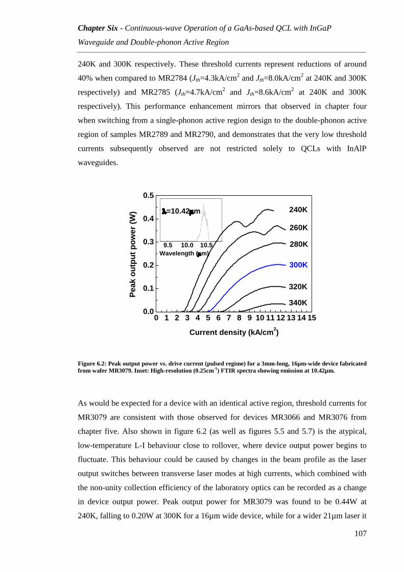
Chapter Six - Continuous-wave Operation of a GaAs-based QCL with InGaP
Waveguide and Double-phonon Active Region
107
240K and 300K respectively. These threshold currents represent reductions of around
40% when compared to MR2784 (Jth=4.3kA/cm2 and Jth=8.0kA/cm
2 at 240K and 300K
respectively) and MR2785 (Jth=4.7kA/cm2 and Jth=8.6kA/cm
2 at 240K and 300K
respectively). This performance enhancement mirrors that observed in chapter four
when switching from a single-phonon active region design to the double-phonon active
region of samples MR2789 and MR2790, and demonstrates that the very low threshold
currents subsequently observed are not restricted solely to QCLs with InAlP
waveguides.
0 1 2 3 4 5 6 7 8 9 10 11 12 13 14 150.0
0.1
0.2
0.3
0.4
0.5
9.5 10.0 10.5
Peak o
utp
ut
po
wer
(W)
Current density (kA/cm2)
240K
260K
280K
300K
320K
340K
Wavelength (m)
=10.42m
Figure 6.2: Peak output power vs. drive current (pulsed regime) for a 3mm-long, 16µm-wide device fabricated
from wafer MR3079. Inset: High-resolution (0.25cm-1) FTIR spectra showing emission at 10.42µm.
As would be expected for a device with an identical active region, threshold currents for
MR3079 are consistent with those observed for devices MR3066 and MR3076 from
chapter five. Also shown in figure 6.2 (as well as figures 5.5 and 5.7) is the atypical,
low-temperature L-I behaviour close to rollover, where device output power begins to
fluctuate. This behaviour could be caused by changes in the beam profile as the laser
output switches between transverse laser modes at high currents, which combined with
the non-unity collection efficiency of the laboratory optics can be recorded as a change
in device output power. Peak output power for MR3079 was found to be 0.44W at
240K, falling to 0.20W at 300K for a 16µm wide device, while for a wider 21µm laser it

Chapter Six - Continuous-wave Operation of a GaAs-based QCL with InGaP
Waveguide and Double-phonon Active Region
108
varied from 0.72W to 0.31W at 240K and 300K respectively. These powers compare
favourably with the devices presented in chapter five, where maximum output was
measured at 0.36W at 240K (MR3069) and 0.13W at 300K (MR3076), although they do
not match those observed for MR2784 - 1.58W and 0.56W at room and low-
temperature respectively. Figure 6.3 shows the calculated characteristic temperature for
MR3079 of T0=90±13K, which is consistent with all devices presented in chapter four.
240 260 280 300 320 3402
3
4
5
6
7
8
Jth
(k
A/c
m2)
Temperature (K)
T0=90K
Figure 6.3: Threshold current density vs. operating temperature for a 3mm-long, 16µm-wide QCL fabricated
from MR3079. The linear fit yields a characteristic temerature of T0=90K.
The reduction in Jth that is observed for MR3079 represents the achievement of one aim
of the decision to combine a double-phonon active region with an InGaP waveguide. A
second desired outcome was a reduction in the large operating voltages that are a feature
of devices incorporating InAlP waveguides, and shown in figure 6.4 are the I-V
characteristics for a 16µm-wide device at both room temperature and 80K. From the
data it is immediately apparent that operating voltages are reduced in comparison to the
InAlP devices featured in chapter five, with voltage at room-temperature threshold
(Jth=5.0kA/cm2) measured at 15.7V. This represents a reduction of ~6.5V when
compared to MR3076 (which had the lowest measured voltage at threshold). This
voltage reduction is maintained over the entire operating range of the device, where at
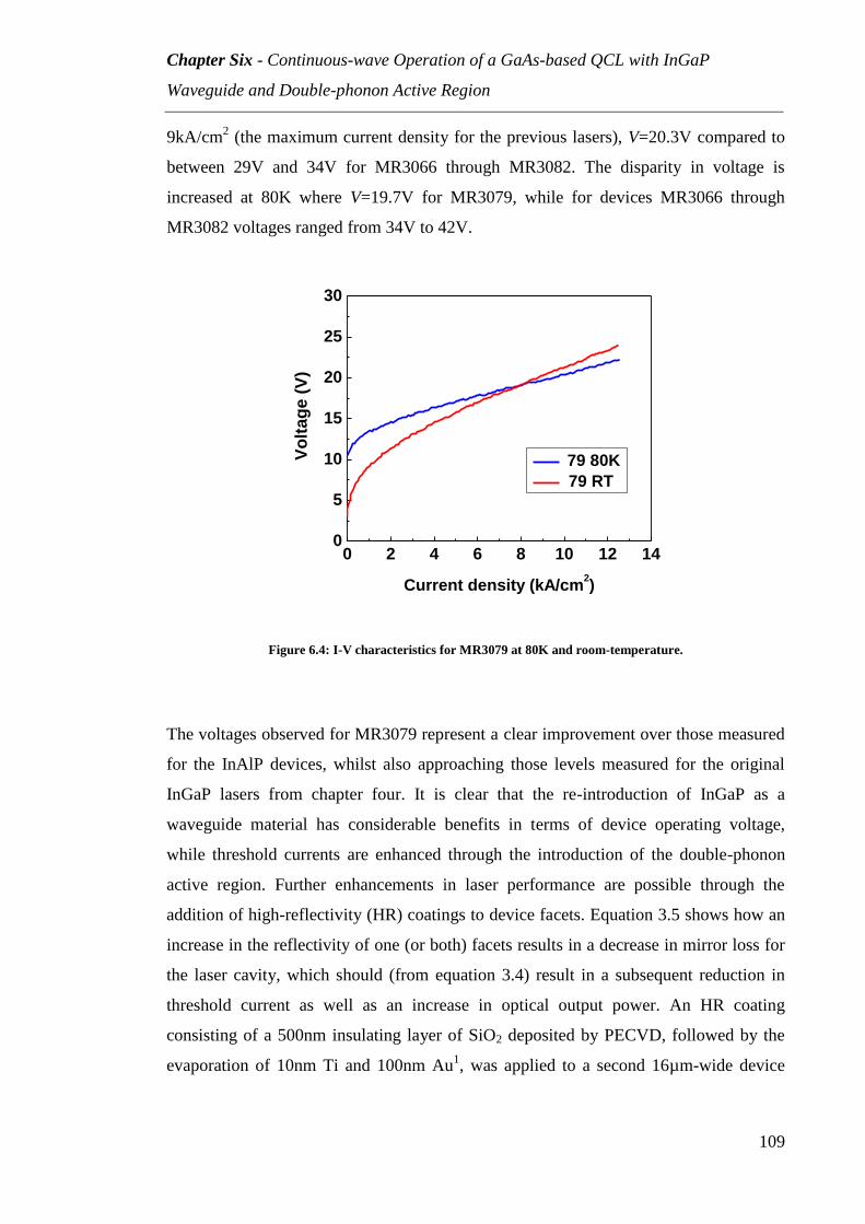
Chapter Six - Continuous-wave Operation of a GaAs-based QCL with InGaP
Waveguide and Double-phonon Active Region
109
9kA/cm2 (the maximum current density for the previous lasers), V=20.3V compared to
between 29V and 34V for MR3066 through MR3082. The disparity in voltage is
increased at 80K where V=19.7V for MR3079, while for devices MR3066 through
MR3082 voltages ranged from 34V to 42V.
0 2 4 6 8 10 12 140
5
10
15
20
25
30
79 80K
79 RT
Vo
ltag
e (
V)
Current density (kA/cm2)
Figure 6.4: I-V characteristics for MR3079 at 80K and room-temperature.
The voltages observed for MR3079 represent a clear improvement over those measured
for the InAlP devices, whilst also approaching those levels measured for the original
InGaP lasers from chapter four. It is clear that the re-introduction of InGaP as a
waveguide material has considerable benefits in terms of device operating voltage,
while threshold currents are enhanced through the introduction of the double-phonon
active region. Further enhancements in laser performance are possible through the
addition of high-reflectivity (HR) coatings to device facets. Equation 3.5 shows how an
increase in the reflectivity of one (or both) facets results in a decrease in mirror loss for
the laser cavity, which should (from equation 3.4) result in a subsequent reduction in
threshold current as well as an increase in optical output power. An HR coating
consisting of a 500nm insulating layer of SiO2 deposited by PECVD, followed by the
evaporation of 10nm Ti and 100nm Au1, was applied to a second 16µm-wide device

Chapter Six - Continuous-wave Operation of a GaAs-based QCL with InGaP
Waveguide and Double-phonon Active Region
110
from wafer MR3079, before optical and electrical characterisation, the results of which
are presented in the following section.
6.3.2 MR3079HR - Pulsed Mode Operation
L-I characteristics for the 3mm-long, 16µm-wide HR-coated device are shown in figure
6.5. As expected, the threshold current density has been reduced with Jth=2.3kA/cm2
observed at 240K, rising to Jth=4.6kA/cm2 at 300K. These currents represent a reduction
of ~10% in comparison to the non-HR MR3079 QCLs presented previously, and are
consistent with those measured for MR2790 - which had the lowest observed Jth of all
devices presented in this thesis. Peak output power has increased in comparison to
MR3079, with P=0.73W and P=0.31W observed at 240K and 300K respectively – an
increase of 290mW and 110mW over non-coated lasers.
0 1 2 3 4 5 6 7 8 9 10 11 12 13 140.0
0.1
0.2
0.3
0.4
0.5
0.6
0.7
0.8
10.0 10.5 11.0
Peak o
utp
ut
po
wer
(W)
Current density (kA/cm2)
240K
260K
280K
300K
320K
340K350K
Wavelength (m)
=10.43m
Figure 6.5: Peak output power vs. drive current (pulsed regime) for a 3mm-long, 16µm-wide device with high-
reflectivity coating on the back facet (MR3079HR). Inset: FTIR spectra showing emission at 10.43µm.

Chapter Six - Continuous-wave Operation of a GaAs-based QCL with InGaP
Waveguide and Double-phonon Active Region
111
Peak emission for this device is seen to occur at λ=10.43µm, virtually identical to its
non-coated counterpart as would be expected, while a maximum operating temperature
of 350K is also observed. The characteristic temperature of T0=91±13K (figure 6.6) is
also consistent with that measured for MR3079, as well as the previous devices with
InGaP waveguides featured in chapter four.
240 260 280 300 320 340 3602
3
4
5
6
7
89
10
Jth
(kA
/cm
2)
Temperature (K)
T0=91K
Figure 6.6: Threshold current density vs. operating temperature for MR3079HR, yielding T0=91K.
Electrical characteristics remain essentially unchanged compared to MR3079, with
voltage at room temperature threshold measured as V=15.8V, rising to V=23.1V at
maximum drive current (figure 6.7).

Chapter Six - Continuous-wave Operation of a GaAs-based QCL with InGaP
Waveguide and Double-phonon Active Region
112
0 2 4 6 8 10 120
5
10
15
20
25
79HR 80K
79HR RT
Vo
lta
ge
(V
)
Current density (kA/cm2)
Figure 6.7: I-V characteristics for MR3079HR taken at 80K and room-temperature.
With the operating voltage for MR3079 lowered to levels approaching those observed
for MR2784 and MR2785, and the further reduction in Jth achieved by the addition of
an HR coating, it was decided to test laser operation in the CW regime. Previous
demonstrations of CW operation with InP-based QCLs have utilised either advanced
processing techniques such as the buried heterostructure configuration2-4
, or made use of
highly thermally conductive submount materials such as copper, aluminium nitride or
diamond5-7
. Due to the standard way in which these devices were processed, and the
poor thermal management afforded by the T05 headers on to which they would
normally be soldered, gold-coated aluminium-nitride ceramic tiles were used as an
alternative. In order to further increase the heat extraction from the laser ridges, ~5µm
of electroplated gold was applied to the top contact of a sample of previously fabricated
devices, before addition of the HR coating. For the purposes of testing devices, a row of
HR-coated lasers were then cleaved into individual chips ~420µm wide, each one
encompassing a single laser ridge. These chips were then indium-soldered epi-layer
down onto the AlN tiles and wire-bonded from chip to tile for electrical contact.
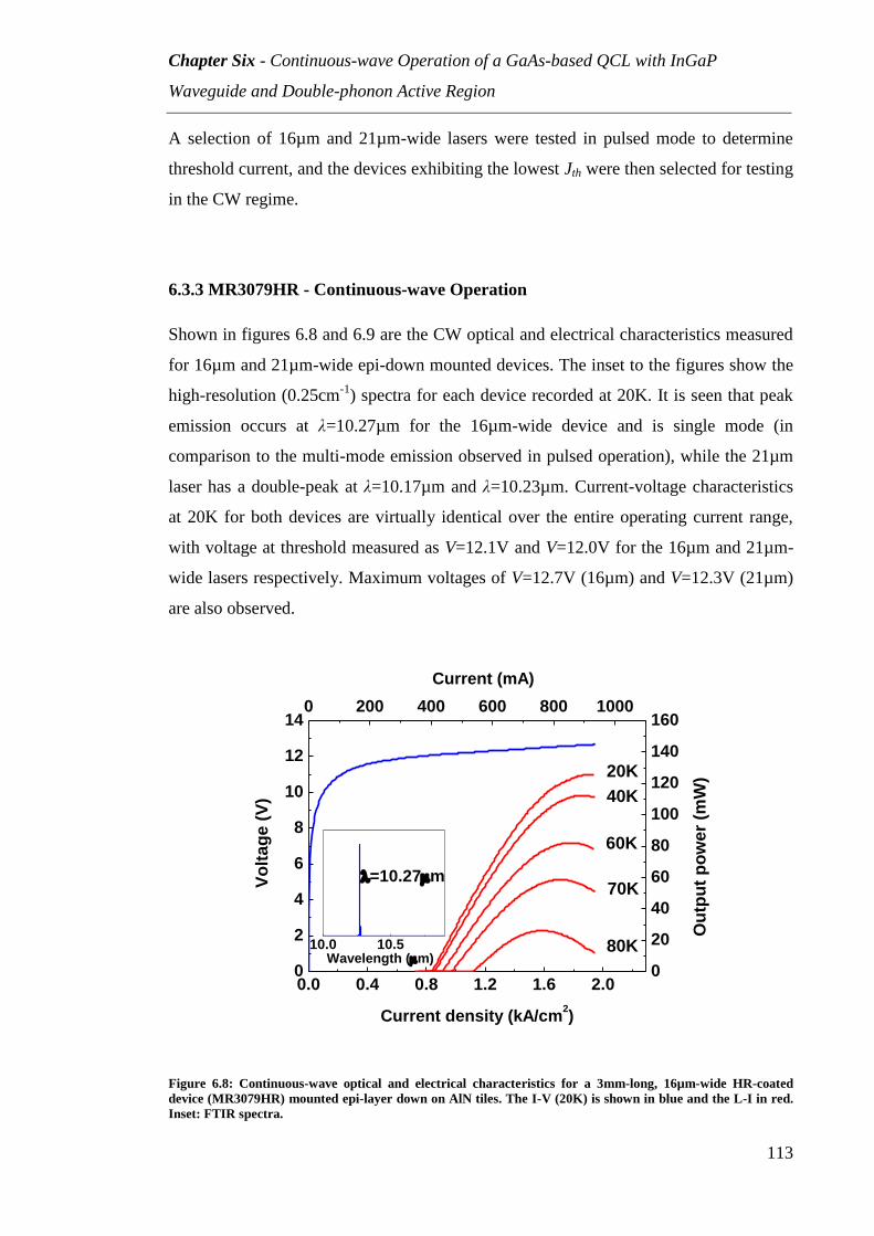
Chapter Six - Continuous-wave Operation of a GaAs-based QCL with InGaP
Waveguide and Double-phonon Active Region
113
A selection of 16µm and 21µm-wide lasers were tested in pulsed mode to determine
threshold current, and the devices exhibiting the lowest Jth were then selected for testing
in the CW regime.
6.3.3 MR3079HR - Continuous-wave Operation
Shown in figures 6.8 and 6.9 are the CW optical and electrical characteristics measured
for 16µm and 21µm-wide epi-down mounted devices. The inset to the figures show the
high-resolution (0.25cm-1
) spectra for each device recorded at 20K. It is seen that peak
emission occurs at λ=10.27µm for the 16µm-wide device and is single mode (in
comparison to the multi-mode emission observed in pulsed operation), while the 21µm
laser has a double-peak at λ=10.17µm and λ=10.23µm. Current-voltage characteristics
at 20K for both devices are virtually identical over the entire operating current range,
with voltage at threshold measured as V=12.1V and V=12.0V for the 16µm and 21µm-
wide lasers respectively. Maximum voltages of V=12.7V (16µm) and V=12.3V (21µm)
are also observed.
0.0 0.4 0.8 1.2 1.6 2.00
2
4
6
8
10
12
140 200 400 600 800 1000
0
20
40
60
80
100
120
140
160
10.0 10.5
Vo
lta
ge
(V
)
Current density (kA/cm2)
Current (mA)O
utp
ut
po
we
r (m
W)20K
40K
60K
70K
80K
Wavelength (m)
=10.27m
Figure 6.8: Continuous-wave optical and electrical characteristics for a 3mm-long, 16µm-wide HR-coated
device (MR3079HR) mounted epi-layer down on AlN tiles. The I-V (20K) is shown in blue and the L-I in red.
Inset: FTIR spectra.

Chapter Six - Continuous-wave Operation of a GaAs-based QCL with InGaP
Waveguide and Double-phonon Active Region
114
Threshold current densities for these devices begin at Jth=0.84kA/cm2 and
Jth=0.77kA/cm2 at 20K for the 16µm and 21µm-wide lasers respectively. These then
rise to Jth=1.1kA/cm2 at the maximum operating temperature of 80K for the 16µm-wide
laser, and Jth=1.0kA/cm2 at 65K for the 21µm-wide device. Peak output powers of
P=126mW at 20K, falling to P=26mW at 80K are observed for the 16µm-wide device,
while P=83mW and P=6mW at 80K and 65K respectively were measured for the wider
laser.
0.0 0.4 0.8 1.2 1.60
2
4
6
8
10
12
140 200 400 600 800 1000
0
10
20
30
40
50
60
70
80
90
100
9.5 10.0 10.5
Vo
ltag
e (
V)
Current density (kA/cm2)
Current (mA)
Ou
tpu
t p
ow
er
(mW
)20K
40K
60K
65K
Wavelength (m)
=10.17m
Figure 6.9: CW optical and electrical characteristics for a 3mm-long, 21µm-wide HR-coated device
(MR3079HR) mounted epi-layer down. The I-V (20K) is shown in blue and the L-I in red. Inset: FTIR spectra.
This CW operation represents the first time such performance has been observed from
GaAs devices at Sheffield, and is only one of a handful of times that CW operation has
been reported for any GaAs-based QCL8-10
. The best performing CW GaAs QCL to-
date, reported by Page and co-workers10
, had a peak output power of 80mW and
threshold current of 470mA (~3.3kA/cm2) at 77K, along with a maximum operating
temperature of 150K. These devices however, used non-standard fabrication techniques
such as proton implantation to limit the current flow through the laser ridge and thus
minimise device heating, as well as omitting an insulating dielectric layer. In view of
Chapter Six - Continuous-wave Operation of a GaAs-based QCL with InGaP
Waveguide and Double-phonon Active Region
115
this, the performance achieved from our standard ridge-processed devices is
encouraging and suggests that with further optimisation, the possibility exists of
exceeding current state of the art CW performance. Possible improvements to consider
include tailoring the width and doping level of the InGaP waveguide to ensure losses are
minimised at the emission wavelength displayed by the lasers, while alterations to the
active region design itself - for example by optimising the spatial nature of the optical
transition - may also result in a further reduction in threshold current density. In terms
of device processing, a switch to a trench configuration rather than the ridge pattern
used in this work could allow a greater volume of electroplated gold to be deposited on
the laser ridges, which in turn should aid the extraction of heat from the ridge during
CW operation. Bonding of these trenched lasers to mounts with a higher thermal
conductivity than AlN should also lead to more efficient heat extraction and allow
devices to operate in CW at higher temperatures.
6.4 Conclusions
The work presented in this section has been concerned with pushing the performance
limits of our GaAs-based QCLs with a view to eventual CW operation. It has been seen
that the reintroduction of InGaP as a waveguide material, combined with a double-
phonon active region results in pulsed regime laser characteristics that in some cases
(i.e. threshold current) exceed current state-of-the-art levels, while in others (e.g. output
power) remain at least comparable. The use of AlN tiles as device mounts, with their
excellent capacity for thermal management, allows advantage to be taken of the reduced
operating voltages and low-temperature threshold currents that are observed for these
devices, and lead to the eventual achievement of CW operation. While the CW
performance by no means matches that of the best CW GaAs devices reported in terms
of output power or maximum operating temperature, the observed low-temperature
threshold currents do in fact represent a reduction compared to those reported by Page et
al10
. It would seem reasonable therefore, to speculate that further improvements in CW
performance could be achieved in future through the combination of improvements
outlined above.

Chapter Six - Continuous-wave Operation of a GaAs-based QCL with InGaP
Waveguide and Double-phonon Active Region
116
1. D. G. Revin, S. Zhang, J. P. Commin, K. Kennedy, A. B. Krysa and J. W. Cockburn, High-Peak-
Power Room-Temperature 3.6m InGaAs-AlAs(Sb) Quantum Cascade Lasers, IEEE Photonics
Technology Letters, 22, 757-759, (2010).
2. M. Beck, D. Hofstetter, T. Aellen, J. Faist, U. Oesterle, M. Ilegems, E. Gini and H. Melchior,
Continuous wave operation of a mid-infrared semiconductor laser at room temperature, Science, 295,
301-305, (2002).
3. D. A. Yarekha, M. Beck, S. Blaser, T. Aellen, E. Gini, D. Hofstetter and J. Faist, Continuous-wave
operation of quantum cascade laser emitting near 5.6m, Electronics Letters, 39, 1123-1125, (2003).
4. T. Aellen, S. Blaser, M. Beck, D. Hofstetter, J. Faist and E. Gini, Continuous-wave distributed-
feedback quantum-cascade lasers on a Peltier cooler, Applied Physics Letters, 83, 1929-1931, (2003).
5. D. Hofstetter, M. Beck, T. Aellen, J. Faist, U. Oesterle, M. Ilegems, E. Gini and H. Melchior,
Continuous wave operation of a 9.3 mu m quantum cascade laser on a Peltier cooler, Applied Physics
Letters, 78, 1964-1966, (2001).
6. J. S. Yu, S. R. Darvish, A. Evans, J. Nguyen, S. Slivken and M. Razeghi, Room-temperature
continuous-wave operation of quantum-cascade lasers at 4m, Applied Physics Letters, 88, 041111,
(2006).
7. J. S. Yu, A. Evans, S. Slivken, S. R. Darvish and M. Razeghi, Temperature dependent
characteristics of 3.8m room-temperature continuous-wave quantum-cascade lasers, Applied Physics
Letters, 88, 251118, (2006).
8. W. Schrenk, N. Finger, S. Gianordoli, E. Gornik and G. Strasser, Continuous-wave operation of
distributed feedback AlAs/GaAs superlattice quantum-cascade lasers, Applied Physics Letters, 77, 3328-
3330, (2000).
9. H. Page, S. Dhillon, M. Calligaro, V. Ortiz and C. Sirtori, Optimised device processing for
continuous-wave operation in GaAs-based quantum cascade lasers, Electronics Letters, 39, 1053-1055,
(2003).
10. H. Page, S. Dhillon, M. Calligaro, C. Becker, V. Ortiz and C. Sirtori, Improved CW operation of
GaAs-Based QC lasers: T-max=150 K, IEEE Journal of Quantum Electronics, 40, 665-672, (2004).

117
Chapter Seven
Conclusions and Future Outlook
This thesis has presented work aimed at advancing the performance of GaAs-based
quantum cascade lasers and their associated waveguide structures. Historically,
improvements in the performance of these devices has not kept pace with those of QCLs
based on the InP material system, and so a strategy involving enhancements to both the
QCL waveguide and active region has been employed in an attempt to address this
disparity. Previous studies had shown that significant reductions in device threshold
current density could be made by replacing the highly-doped GaAs waveguides that are
commonly used in GaAs QCLs, with layers of InGaP. Lowering threshold current is a
vital step on the road to improving the current state-of-the-art CW performance of these
lasers.
Chapter four began by studying the effect that increasing the number of core region
repeat periods of a previously studied GaAs QCL would have on device output. As
expected, a significant increase in optical output power was observed (1.6W peak at
240K) which was interpreted as being a consequence of the increased modal overlap
with the wider device core. A second new QCL design was also studied which
replicated the wider core region, but altered the spatial nature of the optical transition
within the device active region. By moving from a diagonal transition in which the
confined electron states were localised in adjacent quantum wells, to a more vertical
design in which the upper state partially penetrated the lower state well, it was thought
that the intersubband gain could be increased through the large dipole matrix element
associated with vertical optical transitions. The dramatic decrease in output power that
was observed however (0.8W at 240K), suggested that the rather than an increase in
gain, a larger than anticipated reduction in the active region population inversion had
been achieved. This was thought to be a consequence of either a reduced upper state
lifetime (due to the increased transition dipole matrix element), or a reduction in
injection efficiency resulting from the decreased resonance between the upper laser

Chapter Seven - Conclusions and Future Outlook
118
level and the injector level. In order to fully maximise device performance, future
studies may need to include a focus on the optimisation of the spatial characteristics of
the optical transition.
Calculations had suggested that a QCL waveguide consisting of InAlP layers should
theoretically provide an increase in confinement of the optical mode compared to
previous InGaP designs, due to the greater refractive index contrast between waveguide
and core region. Bearing in mind the benefits to laser performance that this confinement
increase might provide, two sets of devices were studied in which the previous InGaP
waveguide layers were replaced by InAlP, with one laser also featuring a redesigned
double-phonon active region. Characterisation of these QCLs revealed further
reductions in threshold current in comparison to the equivalent lasers with InGaP
waveguides, with the double-phonon device exhibiting the lowest threshold current
densities yet observed for any GaAs-based QCL; 2kA/cm2 at 240K and 4kA/cm
2 at
room-temperature. Other device characteristics such as output power were at least
comparable to the previous InGaP QCLs. Despite the low threshold currents however,
all QCLs featuring InAlP waveguides exhibited large operating voltages - in some cases
up to 60V at low temperature - and as a consequence many lasers failed during
operation due to overheating. Those devices that were successfully characterised had to
be done so under relatively low drive currents in order to prevent their failure. It was
suggested that this excess voltage might be related to poor electron flow caused by the
relatively large conduction band offset at the interfaces between the InAlP waveguide
and the surrounding GaAs layers.
Chapter five therefore, focussed on the efforts made to reduce InAlP QCL operating
voltages to more manageable levels. It was hoped that electron flow at the GaAs/InAlP
interfaces could be improved by optimising the transitional layers between the GaAs
and InAlP layers. Two transitional layer designs were tested; the first a superlattice of
InGaP and InAlP and the second a ‘stepped’ design consisting of a thin layer of InGaP
followed by a second thin InAlP layer. Keeping the previous double-phonon active
region design, devices containing one or other of the two transitional layer designs were
characterised in order to ascertain their effect on operating voltage. It was found that
both designs resulted in a voltage reduction of ~12V at room-temperature and ~30V at
80K when compared to the InAlP QCLs from chapter four.

Chapter Seven - Conclusions and Future Outlook
119
In addition to the effects of the transitional layers, a secondary study also looked at how
increasing the aluminium content of several of the AlGaAs barriers within the injector
region to 75% might affect the high-temperature performance of devices. This alteration
to the core region was an attempt to limit the escape of electrons from the upper laser
level into continuum states above the injector region. No performance enhancements
were observed for these devices, and in some cases threshold currents were found to
increase in comparison to devices with standard Al0.45Ga0.55As barriers. It was thought
that the high-Al content of the barriers was creating an escape channel for electrons in
the form of X-valley states within the injector region. These states would decrease the
overall efficiency of the active region and possibly counteract any potential advantages
associated with the high-Al blocking barriers. A systematic study involving changes in
barrier composition and X-valley position, and observation of the associated effects on
device performance would be required to confirm this.
Although the reductions in operating voltage that were achieved through use of the
transitional layers represented a positive progression, the voltages observed were still
significantly higher than of earlier QCLs with InGaP waveguides. In addition to this,
threshold currents were increased in comparison to the InAlP devices described in
chapter four. If further performance enhancements are to be made, it would appear that
future studies should include a concerted effort to fully understand the nature of the
GaAs/InAlP interface, and the underlying causes of the excessive voltages that appear
to be a consequence of the inclusion of InAlP. Determination of the precise nature of the
conduction band profile at the GaAs/InAlP interfaces would be a useful endeavour in
this regard, perhaps through methods such as the capacitance-voltage technique, or it
may be possible to directly measure the voltage drops across the waveguide using
Kelvin probe force microscopy (KFPM). The design of the InAlP waveguide could be
altered somewhat, for example by thinning the InAlP layers in order to improve the
flow of electrons through the structure, however this would come at a cost of increasing
waveguide losses and may reduce some of the performance gains previously observed.
With the varied success achieved by using InAlP as a waveguide material, a reappraisal
of InGaP was deemed appropriate in view of the low operating voltages that had
previously been observed for InGaP waveguide devices in chapter four. Chapter six
therefore, described how the successful double-phonon active region employed in the
low-threshold InAlP QCLs was incorporated into a QCL structure with InGaP

Chapter Seven - Conclusions and Future Outlook
120
waveguide layers, in an attempt to combine the low threshold currents and low
operating voltages previously observed. Initial device characterisation revealed
threshold currents that almost matched those of the InAlP QCLs, while as expected,
operating voltages were reduced by a further 10V, to ~20V at room-temperature. The
addition of a high-reflectivity coating to the back facet of the device led to a further
reduction in threshold current, to a point where it was decided to attempt continuous
wave operation. By utilising epi-layer-down bonding to AlN tiles, CW operation was
observed up to a temperature of 80K - the first time CW lasing from a GaAs-based QCL
had been observed at Sheffield.
Future work aimed at further improving the performance of these devices would be
dependent on the waveguide material being considered. In the case of InGaP, due to the
absence of the large operating voltages that were observed when using InAlP,
immediate changes are likely to focus on improving the way devices are processed, as
these would be relatively straightforward to implement. For example, by switching to a
trench configuration to define the laser ridges and using narrower ridge widths and
improved thermal packaging, heat flow away from the device core could easily be
improved, thus enabling CW operation at higher temperatures. Furthermore, lowering
the device emission wavelength could allow a reduction in waveguide loss and lead to
an additional reduction in threshold current. This lowering of the threshold would also
aid higher-temperature CW device performance.
InAlP has also shown promise as a new waveguide material for GaAs-based QCLs. The
issue of large operating voltages however, must surely be addressed if its full potential
is to be realised. Study of the GaAs/InAlP interfaces and the flow of electrons through
them, would undoubtedly help in the pursuit of a solution to this problem. If voltages
could be reduced to levels similar to those observed with InGaP, utilising the same
changes in device processing outlined above could result in a dramatic leap in
GaAs-based QCL performance. Although it may be some time before GaAs QCLs are
able to match the CW performance of InP-based devices, the work outlined in this thesis
represents very positive progress toward this ultimate goal.

121
Appendices
A1 - Calculation of Conduction Band Profiles and
Electronic Wavefunctions
The conduction band profiles and accompanying electronic wavefunctions presented in
this thesis were produced using ‘ECA’, a software package developed by Roland
Teissier1.
ECA allows the input of a GaAs/AlxGa1-xAs QCL core region structure, using the
thickness of the GaAs wells and AlGaAs barriers as one input parameter, and the
AlxGa1-xAs aluminium fraction (x) as the other. For the purposes of calculating the
electronic wavefunctions and energy levels, the resulting conduction band profile is
placed at the bottom of an infinite potential well, to which an electric field can be
applied depending upon the desired alignment of energy levels. The program
implements the transfer matrix method in order to solve the time-independent
Schrödinger equation for the given potential profile, and return the electronic
wavefuntions ψ(z) and energy levels E for the QCL structure.
The GaAs/AlGaAs conduction band offset ΔEc is calculated using a composition-
dependent quadratic expression:
(A1.1)
where ΔEc is in meV, and x is the AlxGa1-xAs aluminium fraction.

Appendices
122
The effective masses of GaAs and AlxGa1-xAs used by ECA are as follows:
Material Effective mass
GaAs 0.067m0
AlxGa1-xAs (0.067 + 0.042x)m0
Table A1.1: GaAs and AlxGa1-xAs electron effective masses used by the ECA software.
A2 - Calculation of Optical Mode Profiles
The optical mode profiles presented in this thesis were calculated using WGMOD
(H-Scientific Ltd), an application which can determine the TM and TE mode profiles
for a multi-layer structure if the refractive index and thickness of each layer is known.
The refractive index nref, and absorption coefficient k are calculated for each layer using
equations 2.30 to 2.33 (section 2.5), with the following values of effective mass m* and
high-frequency dielectric constant ε∞:
Parameter GaAs Al0.45Ga0.55As In0.49Ga0.51P In0.47Al0.53P
m* (m0) 0.067
2 0.100
2 0.088
2 0.150
3
ε∞ 10.892 9.66
2 9.36
2 8.10
4
Table A2.1: Values of effective mass and high-frequency dielectric constant used in the calculation of
refractive index and absorption coefficient for the QCL structures presented in this thesis.
The remaining parameters contained in equations 2.30 and 2.31 are standard physical
constants, and thus nref and k can be determined for any wavelength λ, and doping
concentration N (the electron scattering time is assumed to be τ=1x10-13
s for all layers5).
For the purposes of modelling, the core region is treated as a single layer with nref and k
determined by an interpolation scheme based on the GaAs/AlGaAs ratio. As an
example, for a wavelength of λ=9µm and using the layer doping levels of samples
MR2785 and MR2789 given in section 4.5, the following values of nref and k for each
layer are obtained:

Appendices
123
Parameter at
λ=9µm
GaAs
Claddings
GaAs
Spacer
GaAs/AlGaAs
Core Region
In0.49Ga0.51P
Waveguide
In0.47Al0.53P
Waveguide
nref 2.76 3.29 3.23 3.05 2.84
k 0.0281 0.000393 0.0000702 0.000322 0.000203
α (cm-1
) 390 5.48 0.980 4.50 2.84
Table A2.2: Refractive index, absorption coefficient and waveguide loss obtained for each layer of samples
MR2785 and MR2789.
These values of nref and k, along with the corresponding layer thicknesses can be used to
generate the required TM mode profile using the WGMOD software:
Figure A2.1: WGMOD software used to calculate optical mode profiles.
For a core region of width L, the overlap factor Γ is calculated simply as the ratio of the
area of the optical mode bounded by the core, to that of the total mode area i.e.6:
∫
∫
(A2.1)

Appendices
124
The waveguide loss associated with each layer of the structure
, is given by7:
(A2.2)
where ω is the angular frequency of emitted radiation and c the speed of light. Thus the
total waveguide loss, for the QCL structure is calculated as the sum of the
individual layer losses,
multiplied by the proportion of the mode penetrating that
layer (where Li is the width of each individual layer):
∑
∫
∫
(A2.3)
Appendices
125
1. Universite Montpellier 2, CNRS, Institut d'Electronique, Montpellier, France,
2. I. P. T. Institute, New Semiconductor Materials: Characteristics and Properties [Online],
Available at: http://www.ioffe.ru/SVA/NSM/Semicond/index.html, (2012).
3. S. Adachi, Properties of Semiconductor Alloys, (Wiley, 2009).
4. T. Hofmann, G. Leibiger, V. Gottschalch, I. Pietzonka and M. Schubert, Infrared dielectric
function and phonon modes of highly disordered (AlxGa1-x)0.52In0.48P, Physical Review B, 64, 155206,
(2001).
5. F. Capasso, A. Y. Cho, J. Faist, A. L. Hutchinson, C. Sirtori and D. L. Sivco, Article Comprising a
Semiconductor Waveguide Structure, United States Patent 5502787, (1996).
6. J. Faist, Quantum Casacde Lasers, (Oxford, 2013).
7. M. Fox, Optical Properties of Solids, (OUP, 2001).