Embed Size (px)
Citation preview
Programmable Logic Devices

PLDs
Programmable Logic Devices (PLD) General purpose chip for implementing circuits Can be customized using programmable switches
Main types of PLDs PLA PAL ROM CPLD FPGA
Custom chips: standard cells, sea of gates
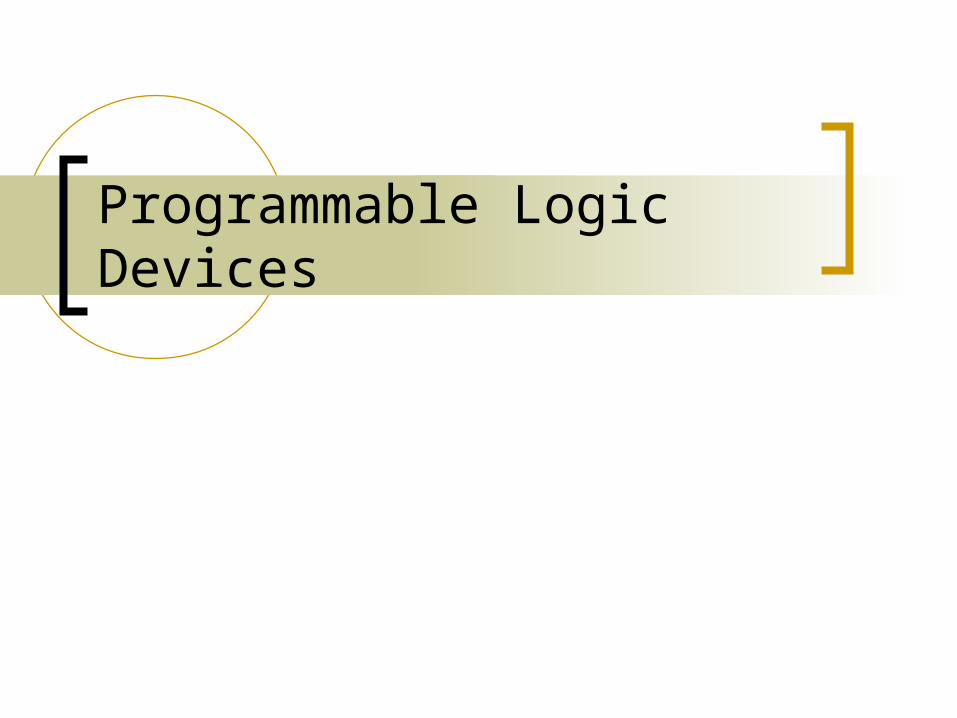
PLD as a Black Box
Logic gates and
programmableswitches
Inputs
(logic variables) Outputs
(logic functions)
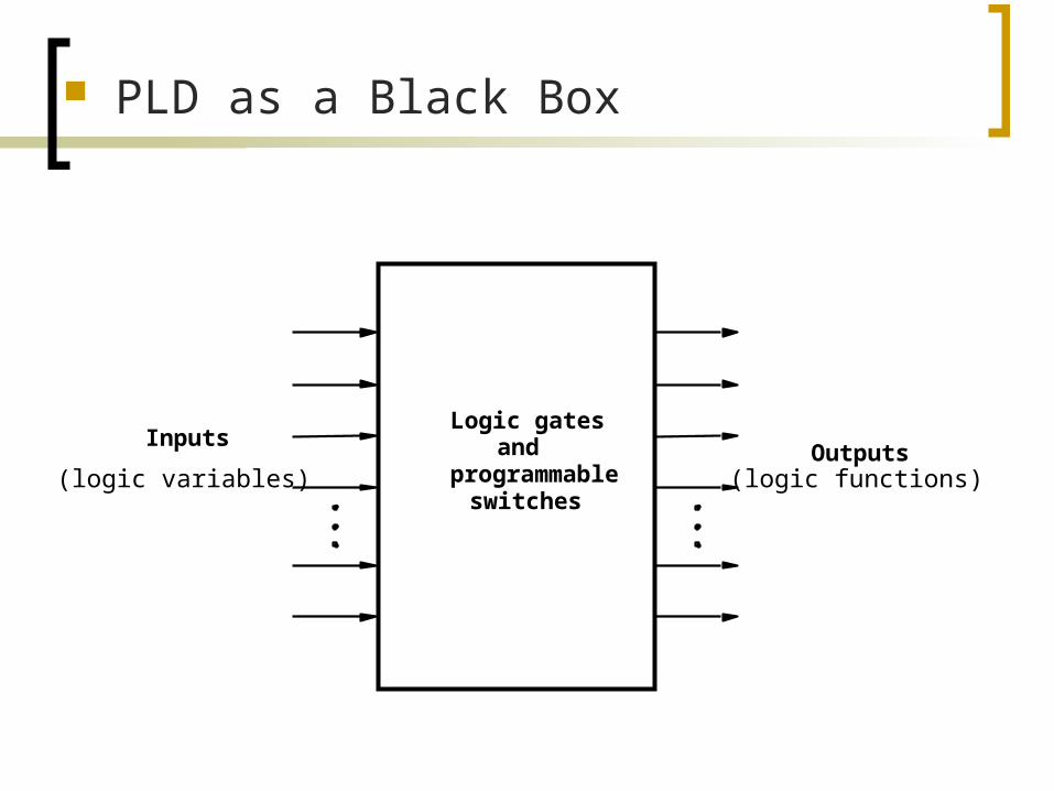
Programmable Logic Array (PLA)
Use to implement circuits in SOP form
The connections inthe AND plane areprogrammable
The connections inthe OR plane areprogrammable
f 1
AND plane OR plane
Input buffers
inverters and
P 1
P k
f m
x 1 x 2 x n
x 1 x 1 x n x n
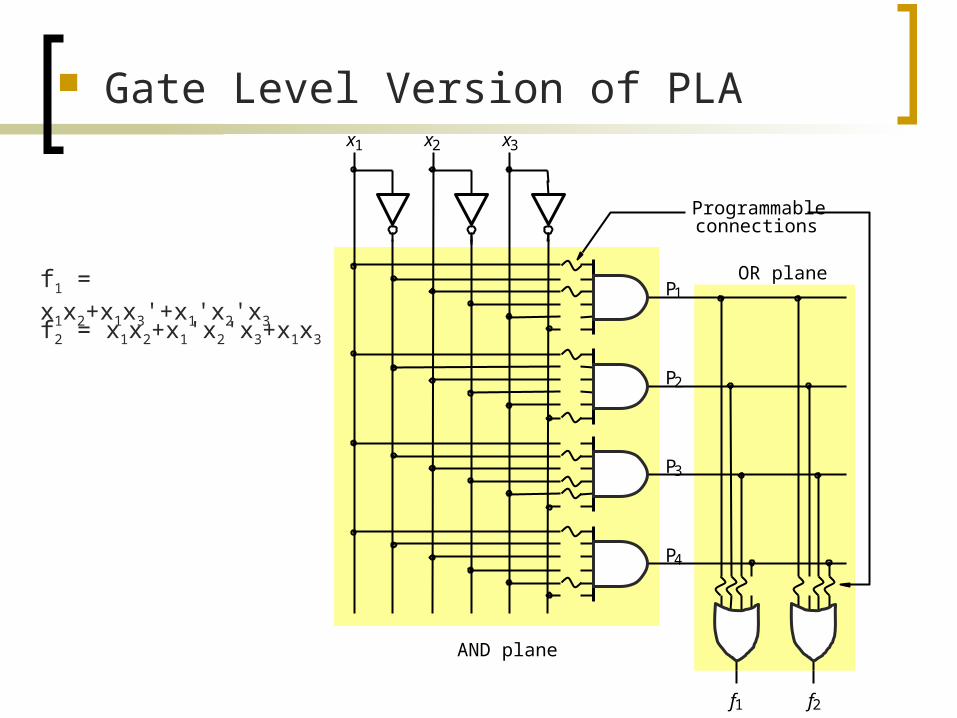
Gate Level Version of PLA
f1
P1
P2
f2
x1 x2 x3
OR plane
Programmable
AND plane
connections
P3
P4
f1 = x1x2+x1x3'+x1'x2'x3
f2 = x1x2+x1'x2'x3+x1x3
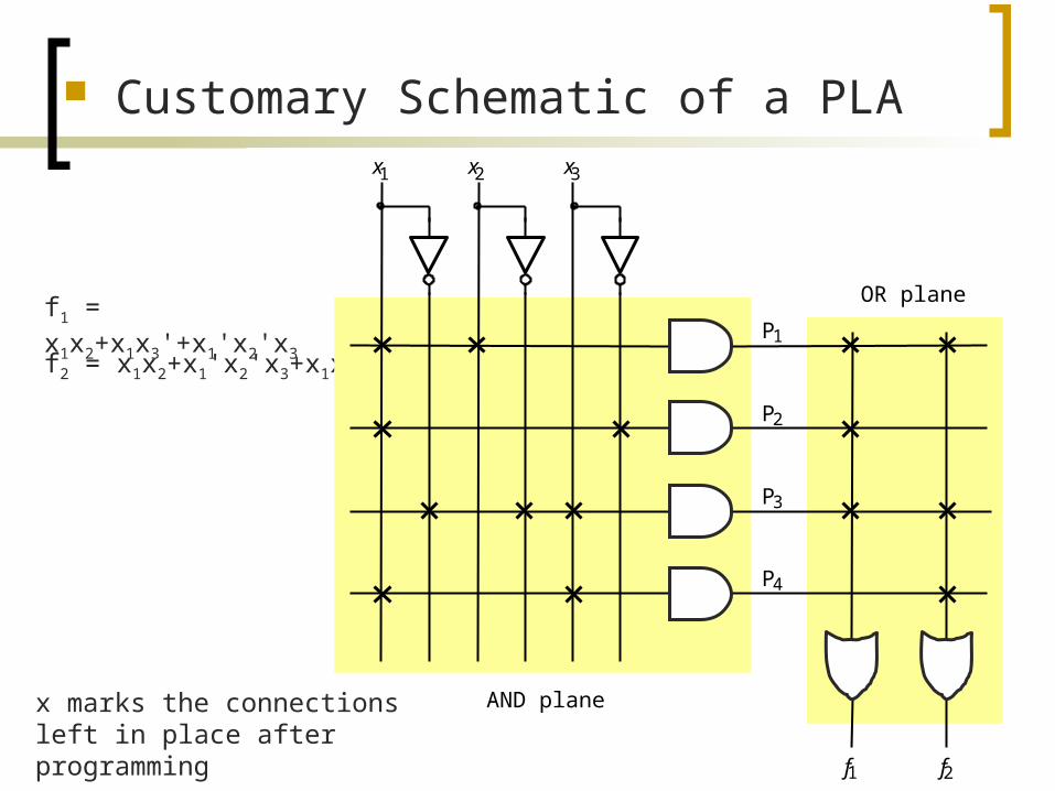
Customary Schematic of a PLA
f1 = x1x2+x1x3'+x1'x2'x3
f2 = x1x2+x1'x2'x3+x1x3
f 1
P 1
P 2
f 2
x 1 x 2 x 3
OR plane
AND plane
P 3
P 4
x marks the connections left in place after programming
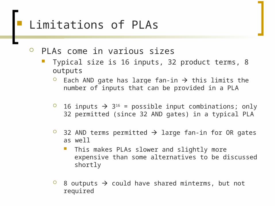
Limitations of PLAs
PLAs come in various sizes Typical size is 16 inputs, 32 product terms, 8 outputs
Each AND gate has large fan-in this limits the number of inputs that can be provided in a PLA
16 inputs 316 = possible input combinations; only 32 permitted (since 32 AND gates) in a typical PLA
32 AND terms permitted large fan-in for OR gates as well This makes PLAs slower and slightly more expensive than
some alternatives to be discussed shortly
8 outputs could have shared minterms, but not required
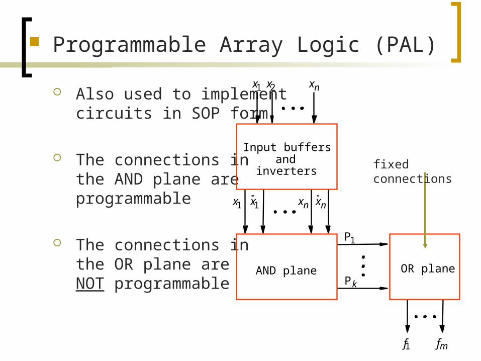
Programmable Array Logic (PAL)
Also used to implement circuits in SOP form
The connections inthe AND plane areprogrammable
The connections inthe OR plane areNOT programmable
f 1
AND plane OR plane
Input buffers
inverters and
P 1
P k
f m
x 1 x 2 x n
x 1 x 1 x n x n
fixed connections
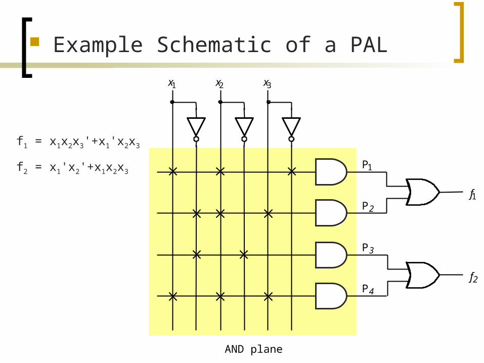
Example Schematic of a PAL
f 1
P 1
P 2
f 2
x 1 x 2 x 3
AND plane
P 3
P 4
f1 = x1x2x3'+x1'x2x3
f2 = x1'x2'+x1x2x3
Comparing PALs and PLAs
PALs have the same limitations as PLAs (small number of allowed AND terms) plus they have a fixed OR plane less flexibility than PLAs
PALs are simpler to manufacture, cheaper, and faster (better performance)
PALs also often have extra circuitry connected to the output of each OR gate The OR gate plus this circuitry is called a macrocell
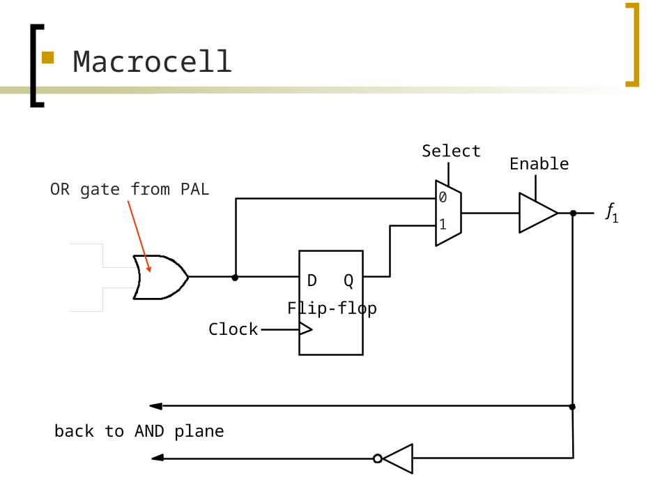
Macrocell
f 1
back to AND plane
D Q
Clock
SelectEnable
Flip-flop
OR gate from PAL 0
1
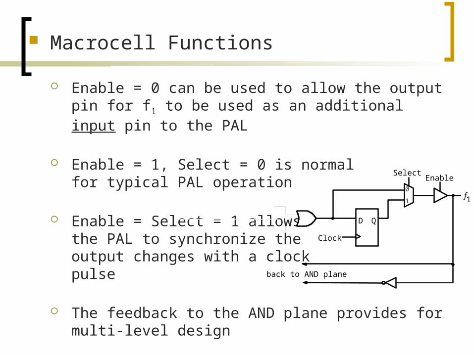
Macrocell Functions
Enable = 0 can be used to allow the output pin for f1 to be used as an additional input pin to the PAL
Enable = 1, Select = 0 is normalfor typical PAL operation
Enable = Select = 1 allowsthe PAL to synchronize the output changes with a clockpulse
The feedback to the AND plane provides for multi-level design
f 1
back to AND plane
D Q
Clock
SelectEnable
0
1
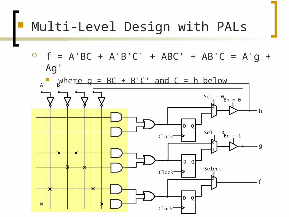
Multi-Level Design with PALs
f = A'BC + A'B'C' + ABC' + AB'C = A'g + Ag' where g = BC + B'C' and C = h below
D Q
Clock
Sel = 0En = 0
0
1
D Q
Clock
Select
0
1
D Q
Clock
Sel = 0En = 1
0
1
A B
h
g
f
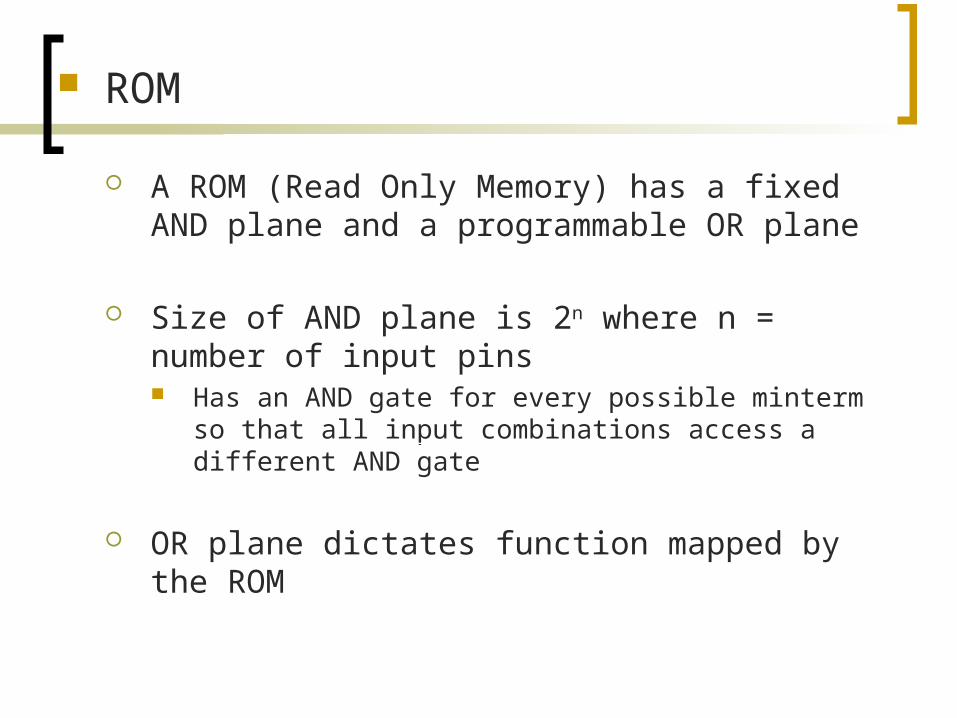
ROM
A ROM (Read Only Memory) has a fixed AND plane and a programmable OR plane
Size of AND plane is 2n where n = number of input pins Has an AND gate for every possible minterm so that all
input combinations access a different AND gate
OR plane dictates function mapped by the ROM
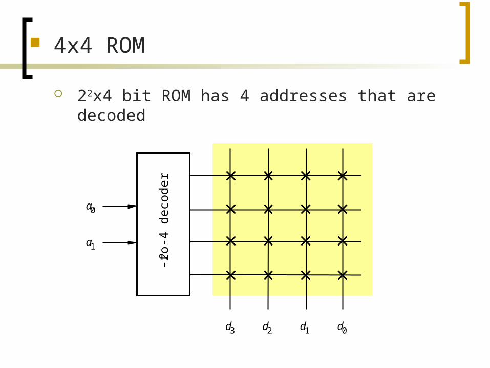
4x4 ROM
22x4 bit ROM has 4 addresses that are decoded
3 d 2 d 1 d 0
2 -to-4
deco
der
a 0
a 1
d
Programming SPLDs
PLAs, PALs, and ROMs are also called SPLDs – Simple Programmable Logic Devices
SPLDs must be programmed so that the switches are in the correct places CAD tools are usually used to do this
A fuse map is created by the CAD tool and then that map is downloaded to the device via a special programming unit
There are two basic types of programming techniques Removable sockets on a PCB In system programming (ISP) on a PCB
This approach is not very common for PLAs and PALs but it is quite common for more complex PLDs
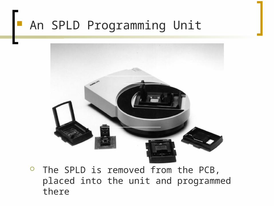
An SPLD Programming Unit
The SPLD is removed from the PCB, placed into the unit and programmed there
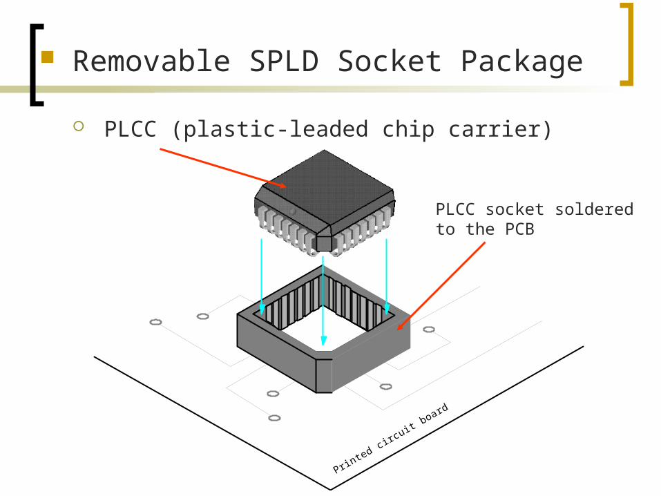
Removable SPLD Socket Package
PLCC (plastic-leaded chip carrier)
Printed cir
cuit board
PLCC socket soldered to the PCB
In System Programming (ISP)
Used when the SPLD cannot be removed from the PCB
A special cable and PCB connection are required to program the SPLD from an attached computer
Very common approach to programming more complex PLDs like CPLDs, FPGAs, etc.
CPLD
Complex Programmable Logic Devices (CPLD)
SPLDs (PLA, PAL) are limited in size due to the small number of input and output pins and the limited number of product terms Combined number of inputs + outputs < 32 or so
CPLDs contain multiple circuit blocks on a single chip Each block is like a PAL: PAL-like block Connections are provided between PAL-like blocks via an
interconnection network that is programmable Each block is connected to an I/O block as well
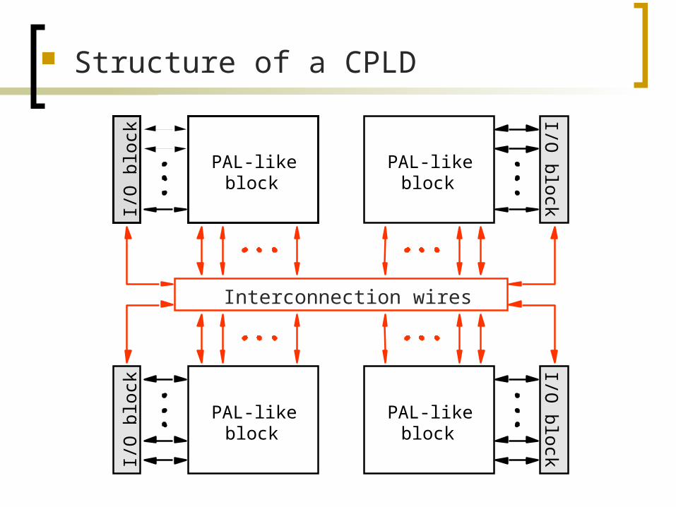
Structure of a CPLD
PAL-likeblock
I/O
blo
ck
PAL-likeblock
I/O b
lock
PAL-likeblock
I/O
blo
ck
PAL-likeblock
I/O b
lock
Interconnection wires
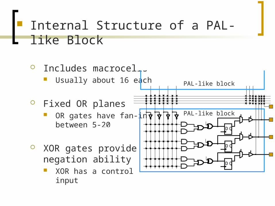
Internal Structure of a PAL-like Block
Includes macrocells Usually about 16 each
Fixed OR planes OR gates have fan-in
between 5-20
XOR gates providenegation ability XOR has a control
input
D Q
D Q
D Q
PAL-like block
PAL-like block
More on PAL-like Blocks
CPLD pins are provided to control XOR, MUX, and tri-state gates
When tri-state gate is disabled, the corresponding output pin can be used as an input pin The associated PAL-like block is then useless
The AND plane and interconnection network are programmable
Commercial CPLDs have between 2-100 PAL-like blocks
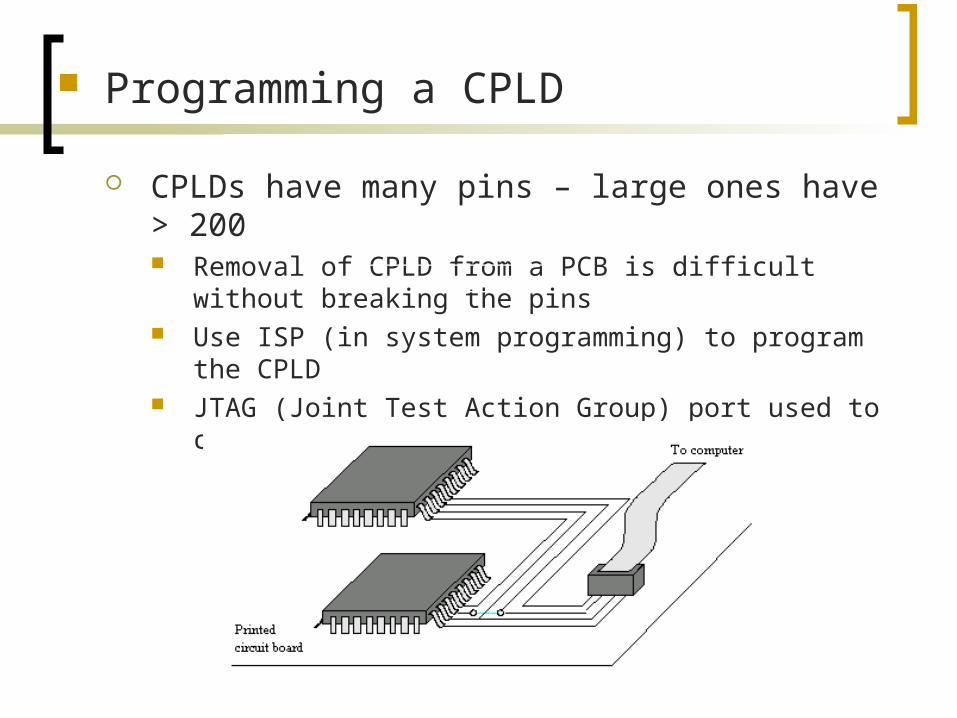
Programming a CPLD
CPLDs have many pins – large ones have > 200 Removal of CPLD from a PCB is difficult without breaking
the pins Use ISP (in system programming) to program the CPLD JTAG (Joint Test Action Group) port used to connect the
CPLD to a computer
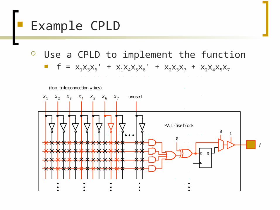
Example CPLD
Use a CPLD to implement the function f = x1x3x6' + x1x4x5x6' + x2x3x7 + x2x4x5x7
D Q
PAL-like block
(from interconnection wires)
x 1 x 2 x 3 x 4 x 5 x 6 x 7 unused
0 0 1
f
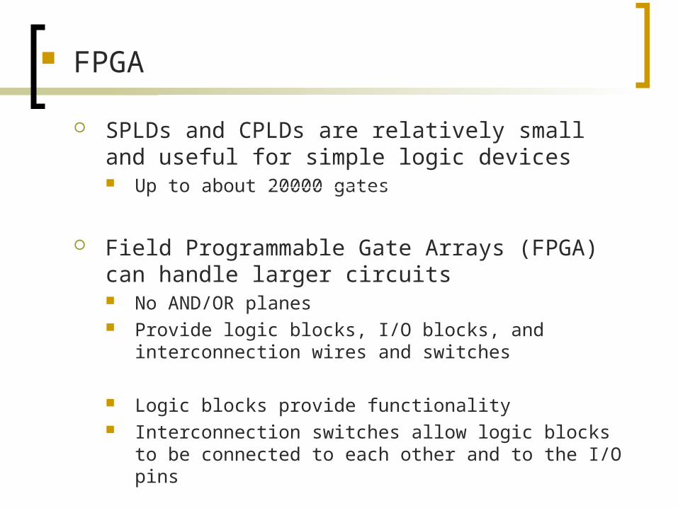
FPGA
SPLDs and CPLDs are relatively small and useful for simple logic devices Up to about 20000 gates
Field Programmable Gate Arrays (FPGA) can handle larger circuits No AND/OR planes Provide logic blocks, I/O blocks, and interconnection wires
and switches
Logic blocks provide functionality Interconnection switches allow logic blocks to be connected
to each other and to the I/O pins
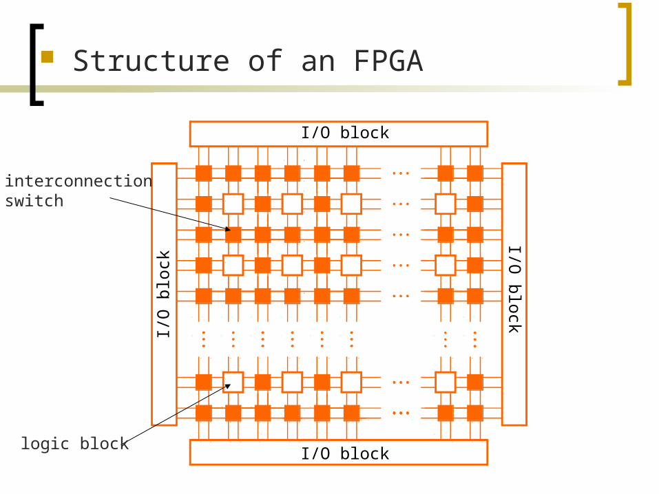
Structure of an FPGA
I/O block
I/O block I/O
blo
ck I/O
blo
ck
logic block
interconnectionswitch
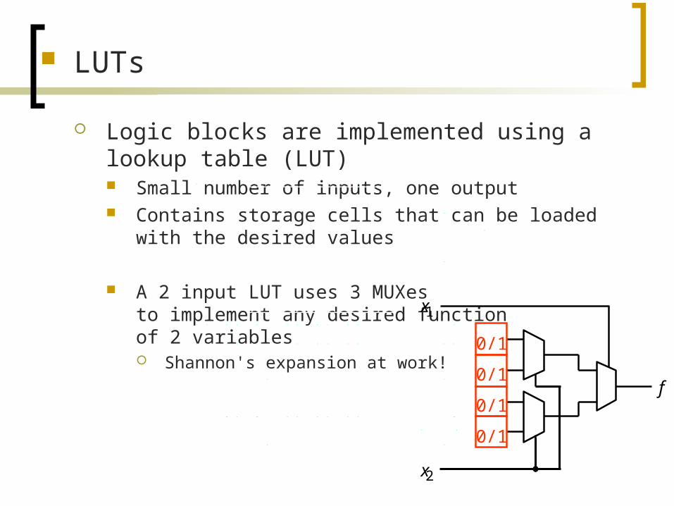
LUTs
Logic blocks are implemented using a lookup table (LUT) Small number of inputs, one output Contains storage cells that can be loaded with the desired
values
A 2 input LUT uses 3 MUXesto implement any desired functionof 2 variables Shannon's expansion at work!
f
0/1
0/1
0/1
0/1
x 1
x 2
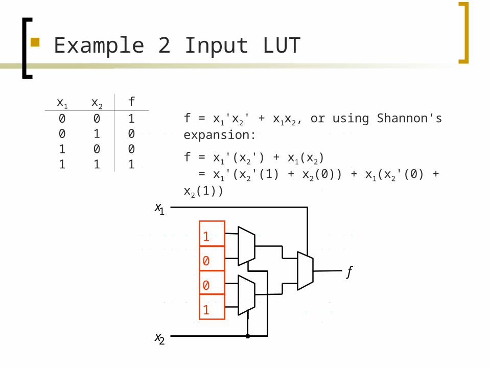
Example 2 Input LUT
x1 x2 f0 0 10 1 01 0 01 1 1
f = x1'x2' + x1x2, or using Shannon's expansion:
f = x1'(x2') + x1(x2) = x1'(x2'(1) + x2(0)) + x1(x2'(0) + x2(1))
f
1
0
0
1
x 1
x 2
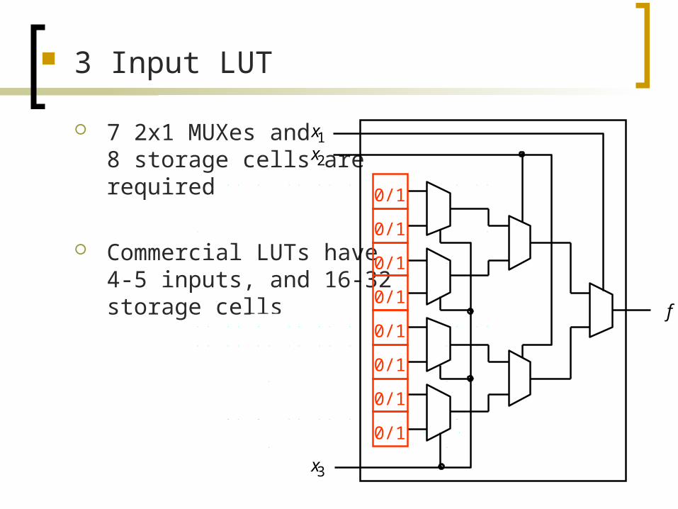
3 Input LUT
7 2x1 MUXes and8 storage cells arerequired
Commercial LUTs have4-5 inputs, and 16-32 storage cells f
0/1
0/1
0/1
0/1
0/1
0/1
0/1
0/1
x 2
x 3
x 1
Programming an FPGA
ISP method is used
LUTs contain volatile storage cells None of the other PLD technologies are volatile FPGA storage cells are loaded via a PROM when power is
first applied
The UP2 Education Board by Altera contains a JTAG port, a MAX 7000 CPLD, and a FLEX 10K FPGA The MAX 7000 CPLD chip is EPM7128SLC84-7 EPM7 MAX 7000 family; 128 macrocells; LC84 84 pin
PLCC package; 7 speed grade
Example FPGA
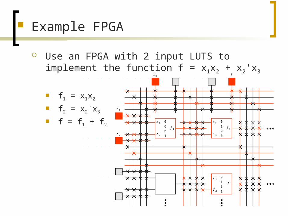
Use an FPGA with 2 input LUTS to implement the function f = x1x2 + x2'x3
f1 = x1x2
f2 = x2'x3
f = f1 + f20 1 0 0
0 1 1 1
0 0 0 1
x 1
x 2
x 2
x 3
f 1
f 2
f 1 f 2
f
x 1
x 2
x 3 f
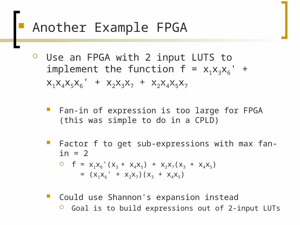
Another Example FPGA
Use an FPGA with 2 input LUTS to implement the function f = x1x3x6' + x1x4x5x6' + x2x3x7 + x2x4x5x7
Fan-in of expression is too large for FPGA (this was simple to do in a CPLD)
Factor f to get sub-expressions with max fan-in = 2 f = x1x6'(x3 + x4x5) + x2x7(x3 + x4x5)
= (x1x6' + x2x7)(x3 + x4x5)
Could use Shannon's expansion instead Goal is to build expressions out of 2-input LUTs
0 0 0 1
0 1 1 1
x 4
x 5
A
B
C
D
x 1
x 6
x 4 f
0 1 1 1
0 0 0 1
x 3
C
D
E
E
f
x 2
x 7
x 5 x 3
0 0 0 1
x 2
x 7
B
0 0 1 0
x 1
x 6
A
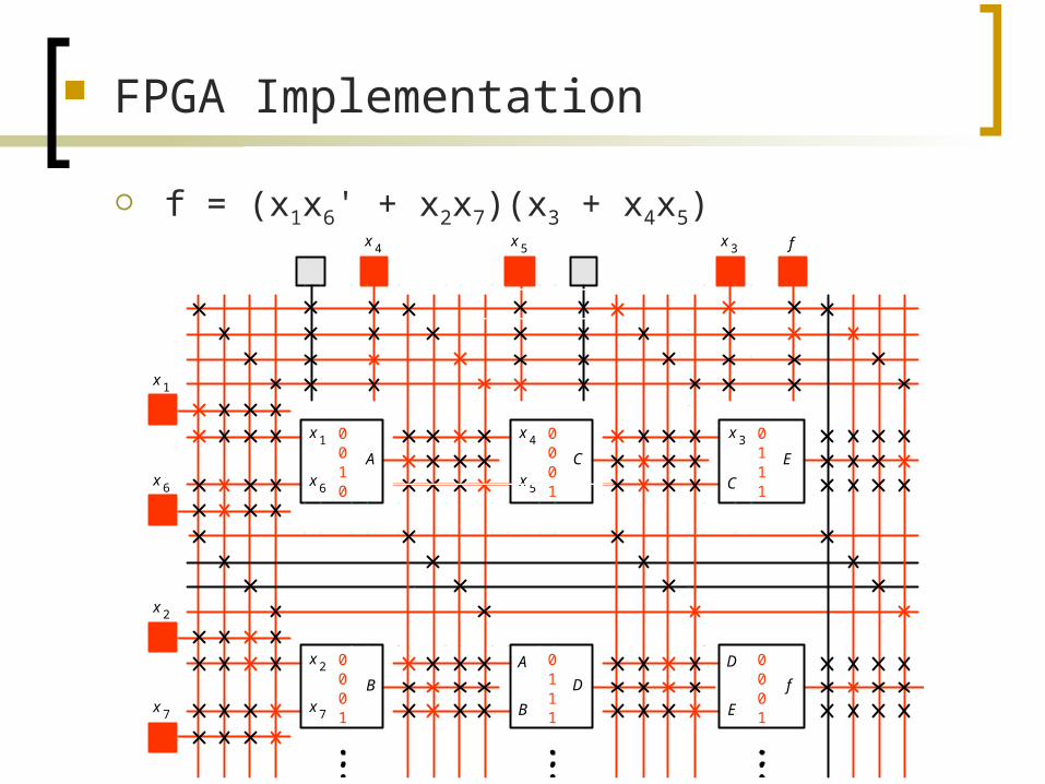
FPGA Implementation
f = (x1x6' + x2x7)(x3 + x4x5)
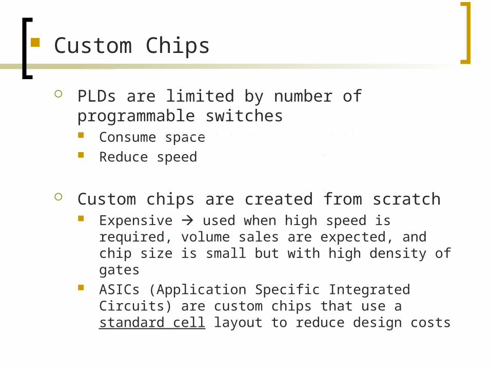
Custom Chips
PLDs are limited by number of programmable switches Consume space Reduce speed
Custom chips are created from scratch Expensive used when high speed is required, volume
sales are expected, and chip size is small but with high density of gates
ASICs (Application Specific Integrated Circuits) are custom chips that use a standard cell layout to reduce design costs
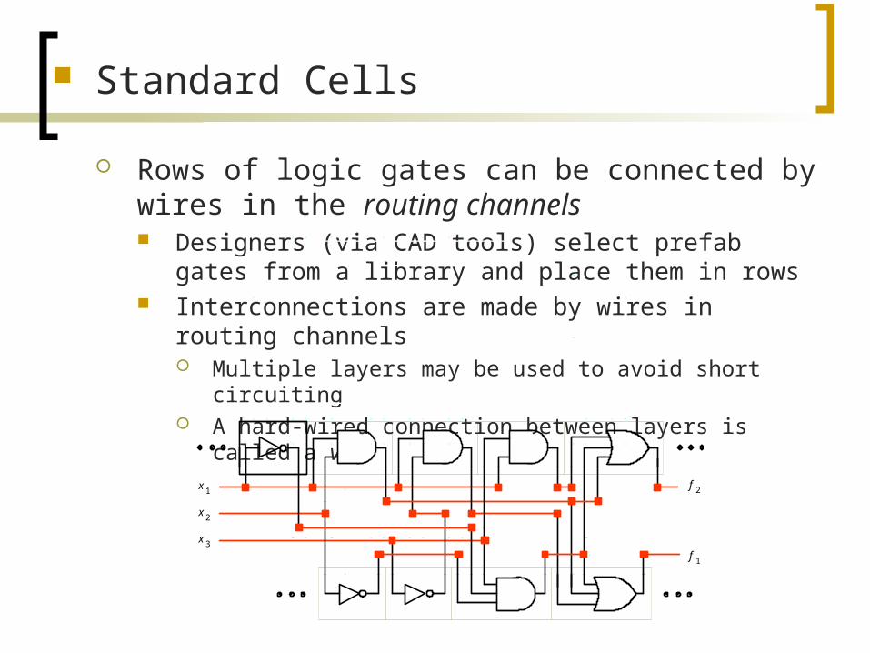
Standard Cells
Rows of logic gates can be connected by wires in the routing channels Designers (via CAD tools) select prefab gates from a library
and place them in rows Interconnections are made by wires in routing channels
Multiple layers may be used to avoid short circuiting A hard-wired connection between layers is called a via
f 1
f 2 x 1
x 3
x 2

Example: Standard Cells
f1 = x1x2 + x1'x2'x3 + x1x3'
f2 = x1x2 + x1'x2'x3 + x1x3
f 1
f 2 x 1
x 3
x 2
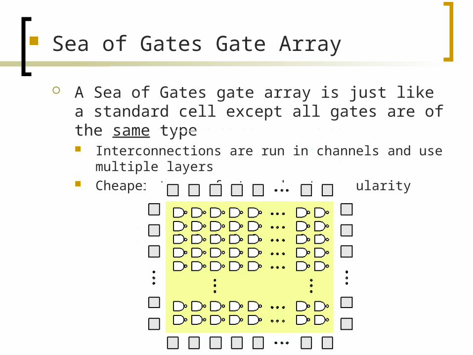
Sea of Gates Gate Array
A Sea of Gates gate array is just like a standard cell except all gates are of the same type Interconnections are run in channels and use multiple
layers Cheaper to manufacture due to regularity
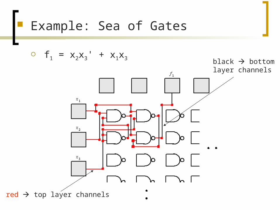
Example: Sea of Gates
f1 = x2x3' + x1x3
red top layer channels
black bottom layer channels
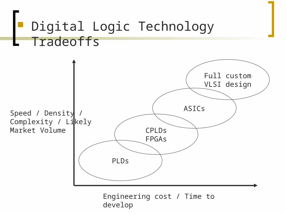
Digital Logic Technology Tradeoffs
Engineering cost / Time to develop
Speed / Density / Complexity / LikelyMarket Volume
PLDs
CPLDsFPGAs
ASICs
Full customVLSI design