Embed Size (px)
Citation preview
Introduction toProgrammable Logic Devices
John CoughlanRAL Technology DepartmentDetector & Electronics Division
[email protected] Design Warrior’s Guide to FPGAs
Devices, Tools, and Flows. ISBN 0750676043Copyright © 2004 Mentor Graphics Corp. (www.mentor.com)
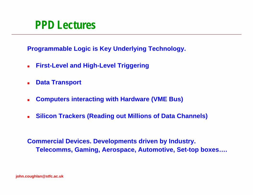
Programmable Logic is Key Underlying Technology.
First-Level and High-Level Triggering
Data Transport
Computers interacting with Hardware (VME Bus)
Silicon Trackers (Reading out Millions of Data Channels)
Commercial Devices. Developments driven by Industry.Telecomms, Gaming, Aerospace, Automotive, Set-top boxes….
PPD Lectures
[email protected] Design Warrior’s Guide to FPGAs
Devices, Tools, and Flows. ISBN 0750676043Copyright © 2004 Mentor Graphics Corp. (www.mentor.com)
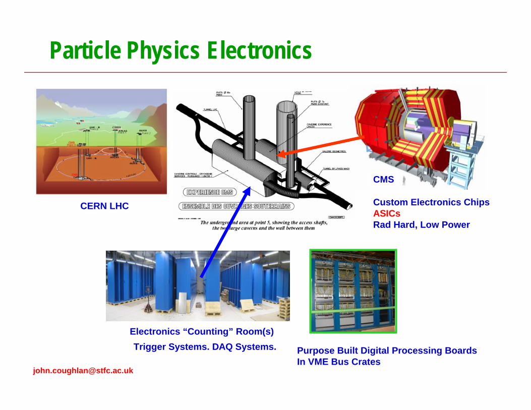
CMS
CERN LHC
Electronics “Counting” Room(s)
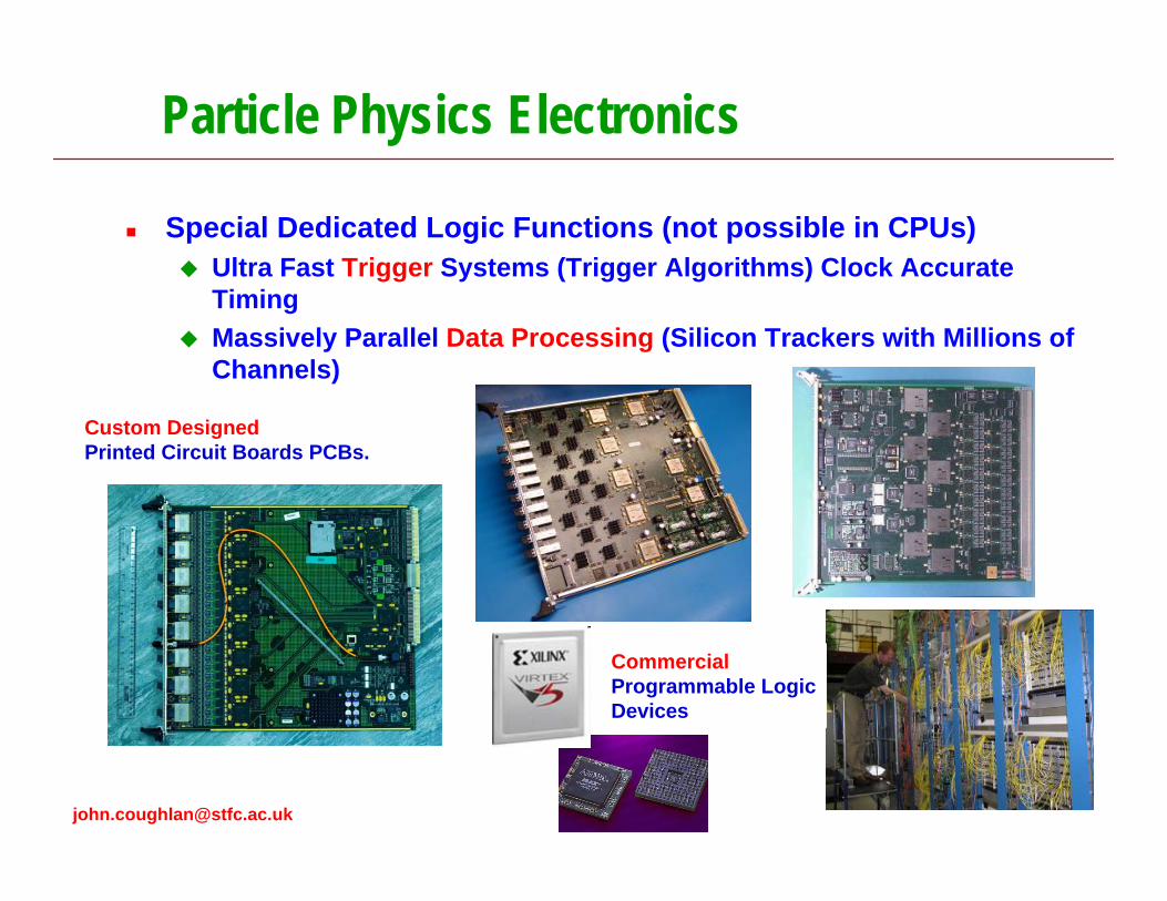
Particle Physics Electronics
Trigger Systems. DAQ Systems.
Custom Electronics ChipsASICsRad Hard, Low Power
Purpose Built Digital Processing BoardsIn VME Bus Crates
[email protected] Design Warrior’s Guide to FPGAs
Devices, Tools, and Flows. ISBN 0750676043Copyright © 2004 Mentor Graphics Corp. (www.mentor.com)
Particle Physics Electronics
Special Dedicated Logic Functions (not possible in CPUs)Ultra Fast Trigger Systems (Trigger Algorithms) Clock Accurate TimingMassively Parallel Data Processing (Silicon Trackers with Millions of Channels)
Custom DesignedPrinted Circuit Boards PCBs.
CommercialProgrammable LogicDevices
[email protected] Design Warrior’s Guide to FPGAs
Devices, Tools, and Flows. ISBN 0750676043Copyright © 2004 Mentor Graphics Corp. (www.mentor.com)
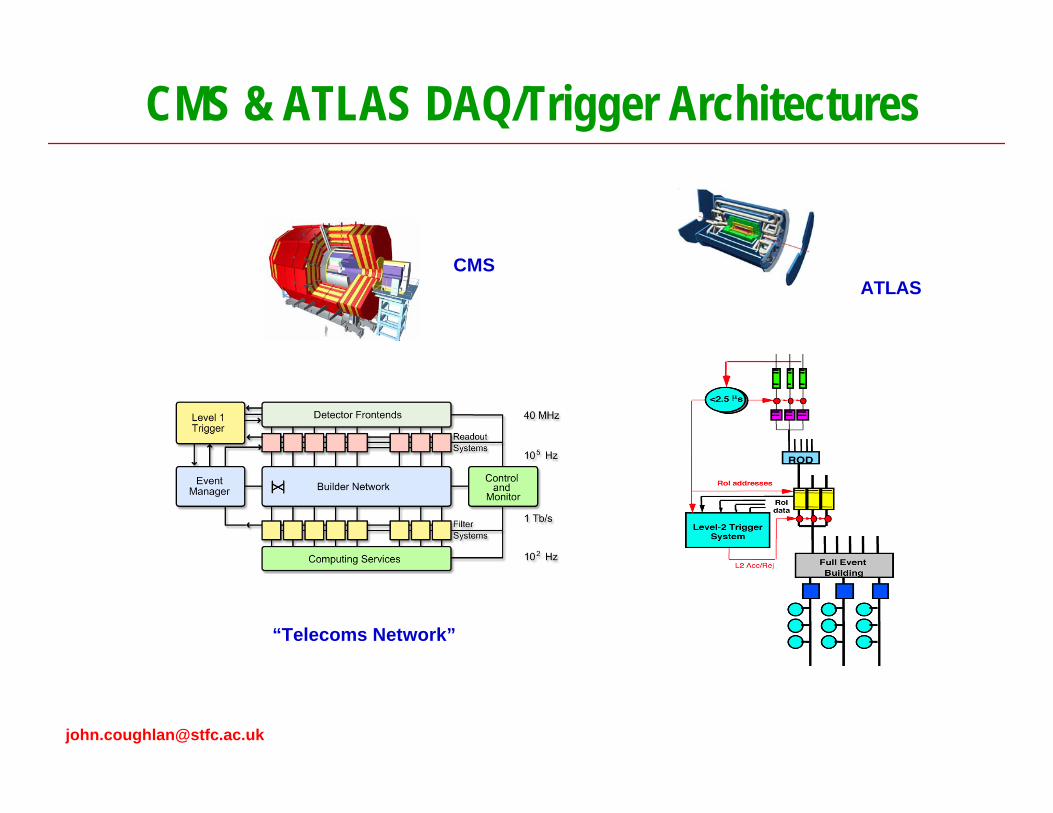
CMS & ATLAS DAQ/Trigger Architectures
CMSATLAS
“Telecoms Network”
[email protected] Design Warrior’s Guide to FPGAs
Devices, Tools, and Flows. ISBN 0750676043Copyright © 2004 Mentor Graphics Corp. (www.mentor.com)
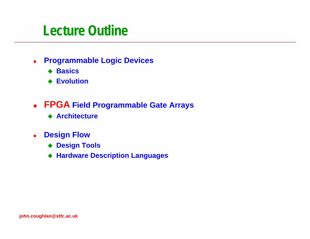
Lecture Outline
Programmable Logic DevicesBasicsEvolution
FPGA Field Programmable Gate ArraysArchitecture
Design FlowDesign ToolsHardware Description Languages
[email protected] Design Warrior’s Guide to FPGAs
Devices, Tools, and Flows. ISBN 0750676043Copyright © 2004 Mentor Graphics Corp. (www.mentor.com)
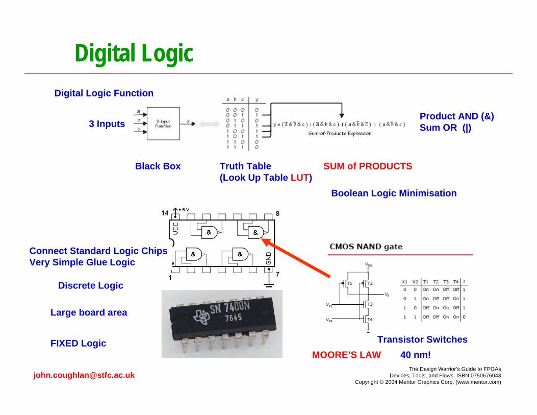
Digital Logic
Connect Standard Logic ChipsVery Simple Glue Logic
Black Box SUM of PRODUCTS
FIXED Logic
Truth Table(Look Up Table LUT)
Boolean Logic Minimisation
Transistor Switches
Digital Logic Function
3 InputsProduct AND (&)Sum OR (|)
Large board area
Discrete Logic
MOORE’S LAW 40 nm!
[email protected] Design Warrior’s Guide to FPGAs
Devices, Tools, and Flows. ISBN 0750676043Copyright © 2004 Mentor Graphics Corp. (www.mentor.com)
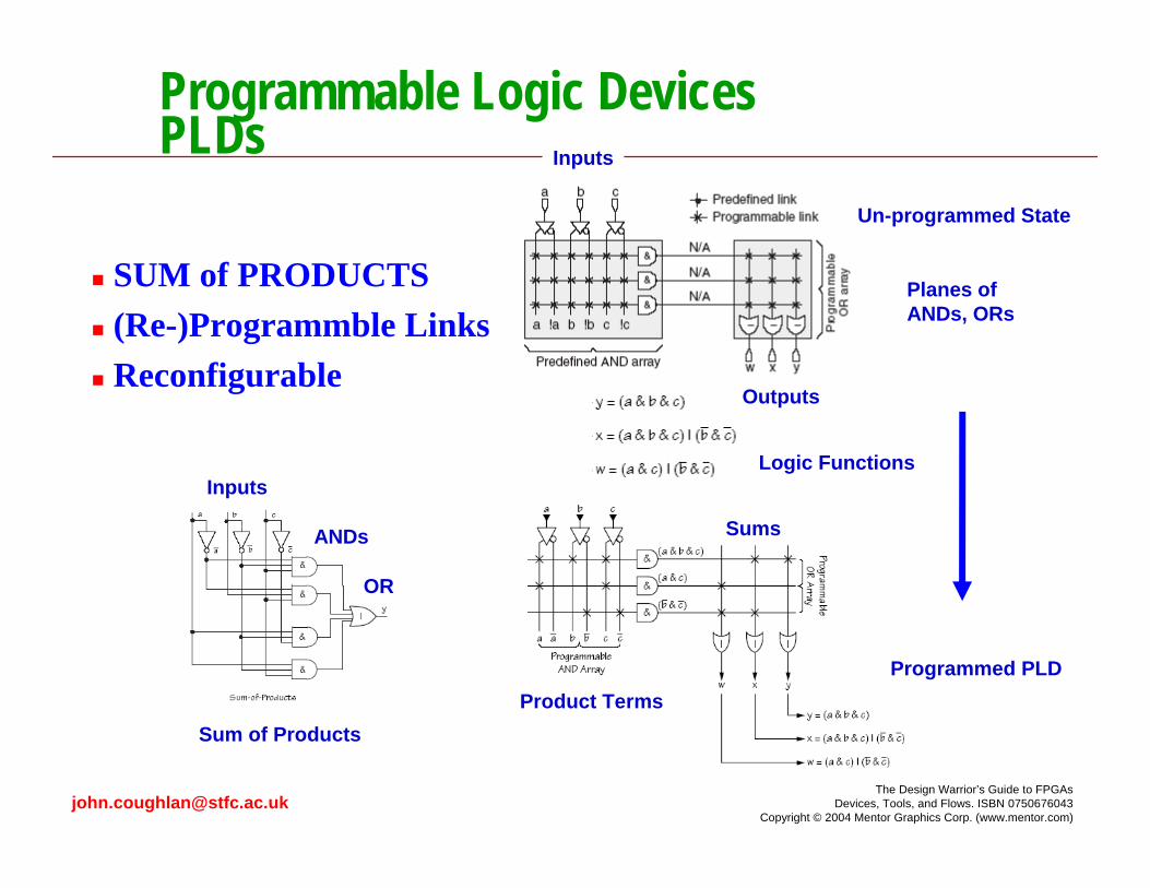
Programmable Logic Devices PLDs
Sum of Products
Un-programmed State
SUM of PRODUCTS(Re-)Programmble LinksReconfigurable
Logic Functions
Programmed PLDProduct Terms
Sums
Planes ofANDs, ORs
ANDs
OR
Inputs
Inputs
Outputs
[email protected] Design Warrior’s Guide to FPGAs
Devices, Tools, and Flows. ISBN 0750676043Copyright © 2004 Mentor Graphics Corp. (www.mentor.com)
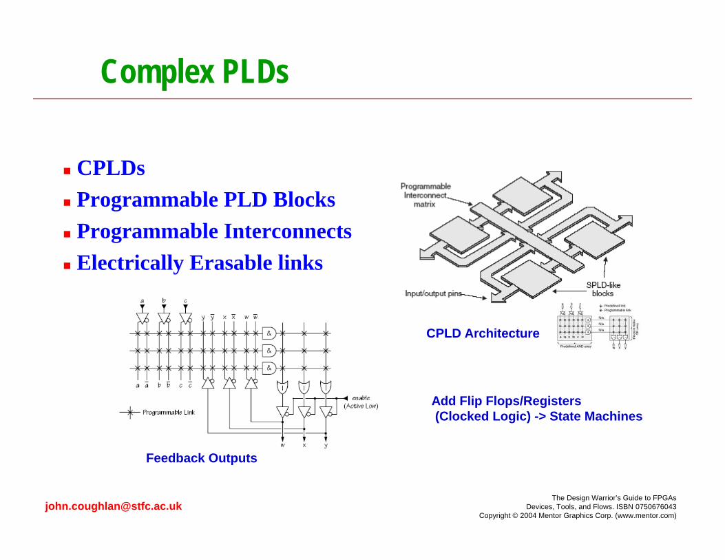
Complex PLDs
CPLDsProgrammable PLD BlocksProgrammable InterconnectsElectrically Erasable links
CPLD Architecture
Feedback Outputs
Add Flip Flops/Registers(Clocked Logic) -> State Machines
[email protected] Design Warrior’s Guide to FPGAs
Devices, Tools, and Flows. ISBN 0750676043Copyright © 2004 Mentor Graphics Corp. (www.mentor.com)
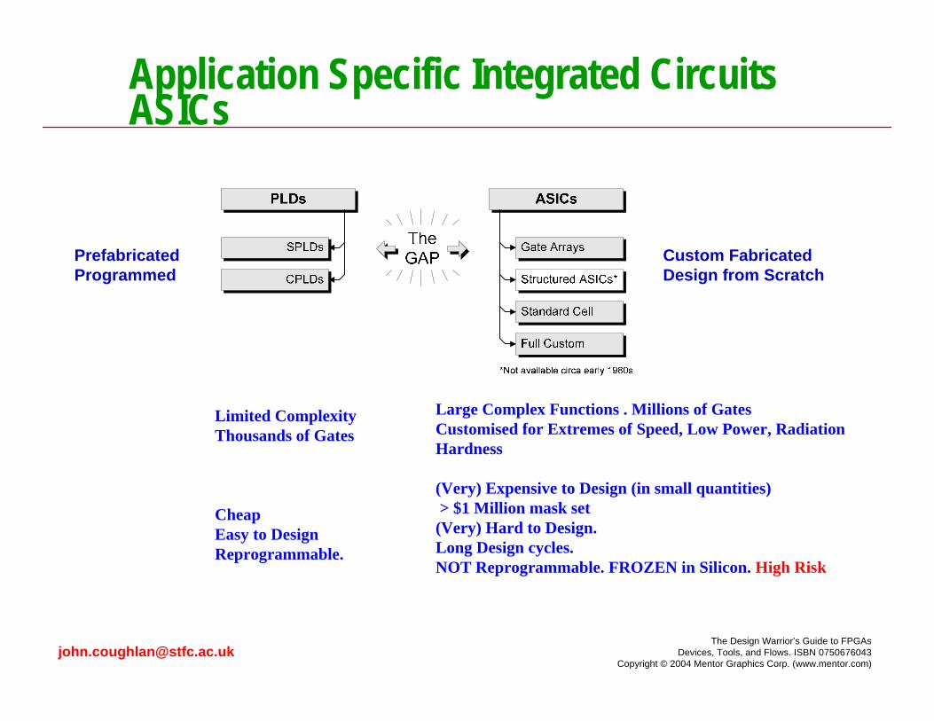
Application Specific Integrated Circuits ASICs
Large Complex Functions . Millions of GatesCustomised for Extremes of Speed, Low Power, Radiation Hardness
(Very) Expensive to Design (in small quantities) > $1 Million mask set(Very) Hard to Design.Long Design cycles.NOT Reprogrammable. FROZEN in Silicon. High Risk
Limited ComplexityThousands of Gates
CheapEasy to DesignReprogrammable.
Custom FabricatedDesign from Scratch
PrefabricatedProgrammed
[email protected] Design Warrior’s Guide to FPGAs
Devices, Tools, and Flows. ISBN 0750676043Copyright © 2004 Mentor Graphics Corp. (www.mentor.com)
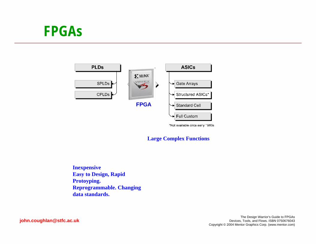
FPGAs
Large Complex Functions
InexpensiveEasy to Design, Rapid Protoyping.Reprogrammable. Changing data standards.
FPGA
[email protected] Design Warrior’s Guide to FPGAs
Devices, Tools, and Flows. ISBN 0750676043Copyright © 2004 Mentor Graphics Corp. (www.mentor.com)
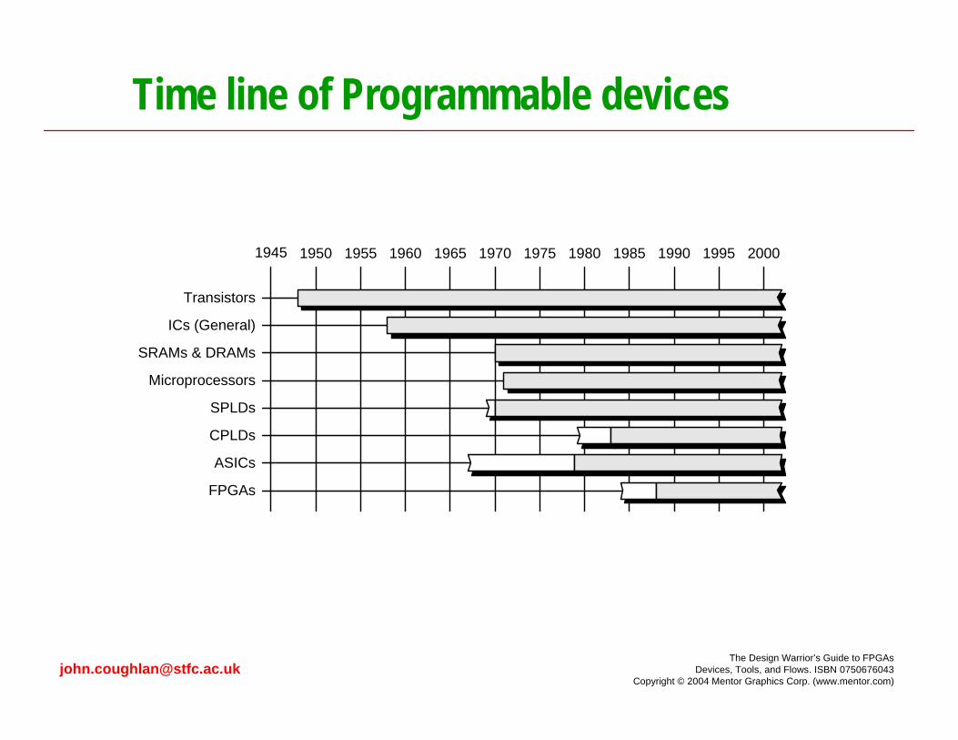
Time line of Programmable devices
1945 1950 1955 1960 1965 1970 1975 1980 1985 1990 1995 2000
FPGAs
ASICs
CPLDs
SPLDs
Microprocessors
SRAMs & DRAMs
ICs (General)
Transistors
[email protected] Design Warrior’s Guide to FPGAs
Devices, Tools, and Flows. ISBN 0750676043Copyright © 2004 Mentor Graphics Corp. (www.mentor.com)
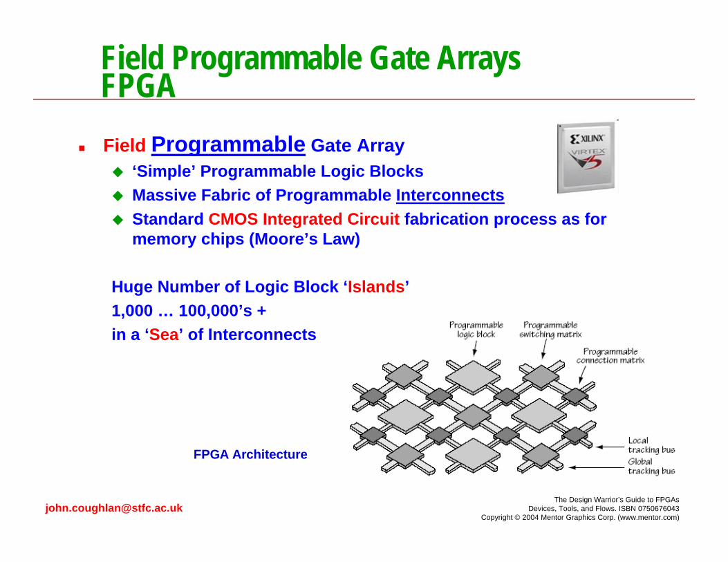
Field Programmable Gate Arrays FPGAField Programmable Gate Array
‘Simple’ Programmable Logic BlocksMassive Fabric of Programmable InterconnectsStandard CMOS Integrated Circuit fabrication process as for memory chips (Moore’s Law)
Huge Number of Logic Block ‘Islands’1,000 … 100,000’s +in a ‘Sea’ of Interconnects
FPGA Architecture
[email protected] Design Warrior’s Guide to FPGAs
Devices, Tools, and Flows. ISBN 0750676043Copyright © 2004 Mentor Graphics Corp. (www.mentor.com)
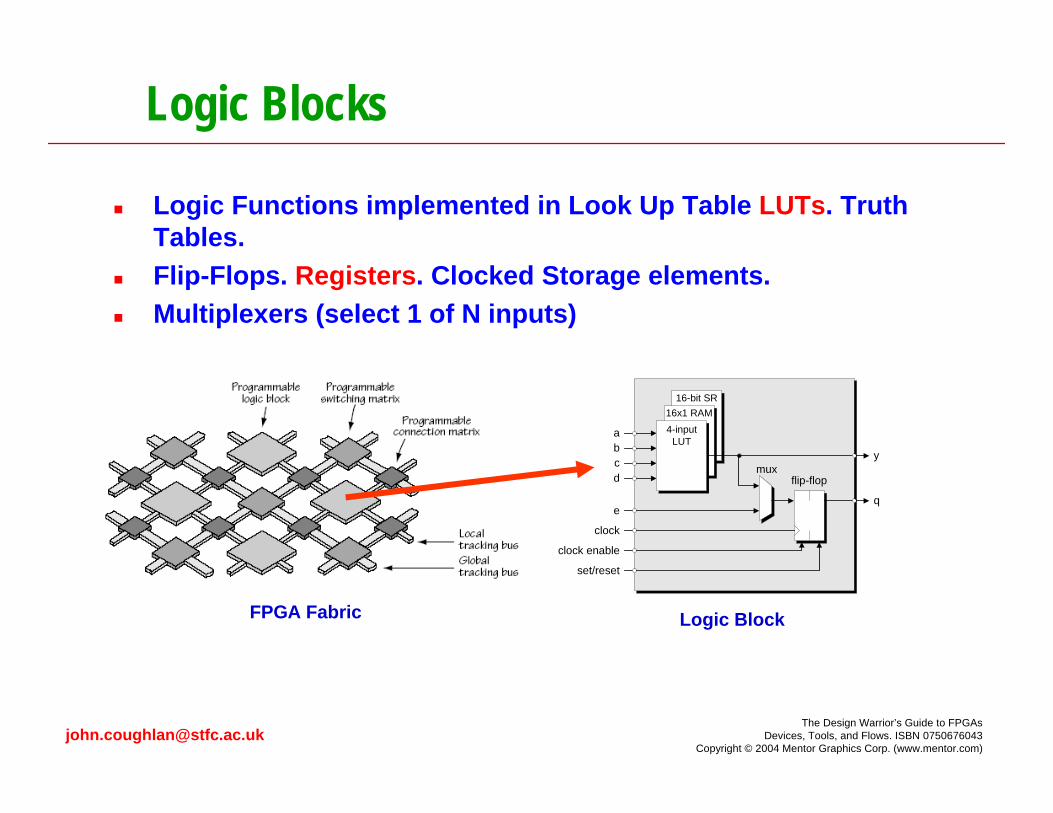
Logic Blocks
Logic Functions implemented in Look Up Table LUTs. Truth Tables.Flip-Flops. Registers. Clocked Storage elements. Multiplexers (select 1 of N inputs)
16-bit SR
flip-flop
clock
muxy
qe
abcd
16x1 RAM4-input
LUT
clock enable
set/reset
FPGA Fabric Logic Block
[email protected] Design Warrior’s Guide to FPGAs
Devices, Tools, and Flows. ISBN 0750676043Copyright © 2004 Mentor Graphics Corp. (www.mentor.com)
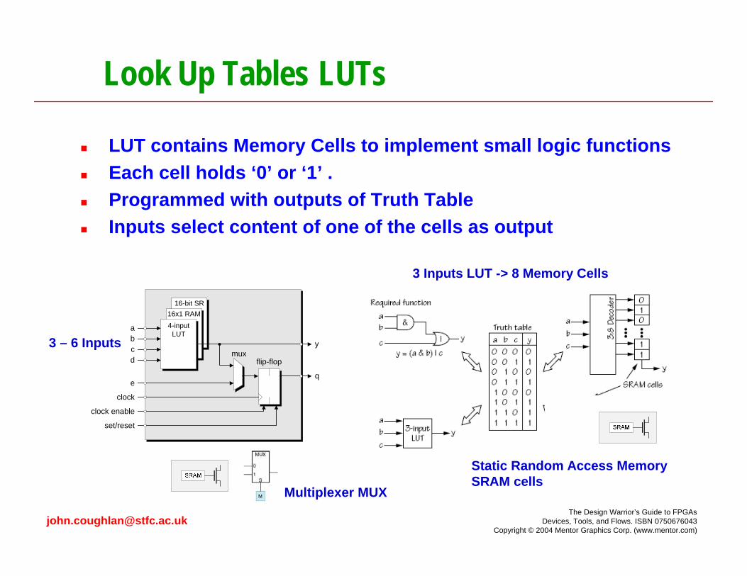
Look Up Tables LUTs
LUT contains Memory Cells to implement small logic functionsEach cell holds ‘0’ or ‘1’ .Programmed with outputs of Truth TableInputs select content of one of the cells as output
16-bit SR
flip-flop
clock
muxy
qe
abcd
16x1 RAM4-input
LUT
clock enable
set/reset
3 Inputs LUT -> 8 Memory Cells
Static Random Access MemorySRAM cells
3 – 6 Inputs
Multiplexer MUX
[email protected] Design Warrior’s Guide to FPGAs
Devices, Tools, and Flows. ISBN 0750676043Copyright © 2004 Mentor Graphics Corp. (www.mentor.com)
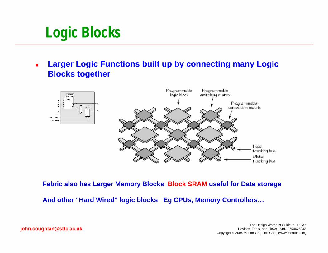
Logic Blocks
Larger Logic Functions built up by connecting many Logic Blocks together
Fabric also has Larger Memory Blocks Block SRAM useful for Data storage
And other “Hard Wired” logic blocks Eg CPUs, Memory Controllers…
[email protected] Design Warrior’s Guide to FPGAs
Devices, Tools, and Flows. ISBN 0750676043Copyright © 2004 Mentor Graphics Corp. (www.mentor.com)
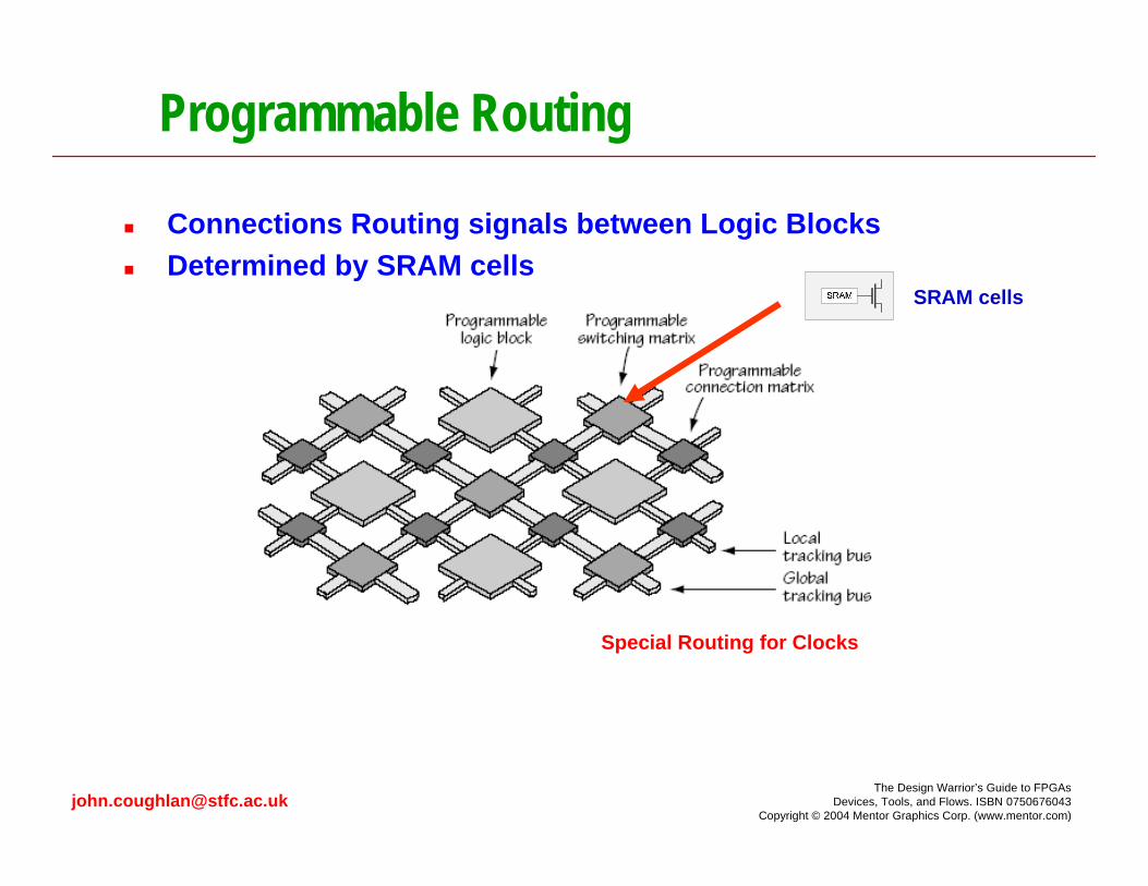
Programmable Routing
Connections Routing signals between Logic BlocksDetermined by SRAM cells
Special Routing for Clocks
SRAM cells
[email protected] Design Warrior’s Guide to FPGAs
Devices, Tools, and Flows. ISBN 0750676043Copyright © 2004 Mentor Graphics Corp. (www.mentor.com)
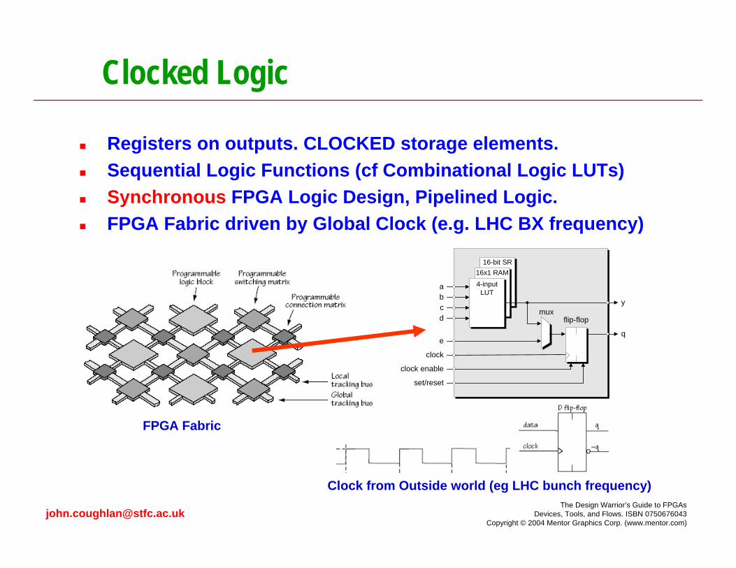
Clocked Logic
Registers on outputs. CLOCKED storage elements.Sequential Logic Functions (cf Combinational Logic LUTs)Synchronous FPGA Logic Design, Pipelined Logic. FPGA Fabric driven by Global Clock (e.g. LHC BX frequency)
16-bit SR
flip-flop
clock
muxy
qe
abcd
16x1 RAM4-input
LUT
clock enable
set/reset
FPGA Fabric
Clock from Outside world (eg LHC bunch frequency)
[email protected] Design Warrior’s Guide to FPGAs
Devices, Tools, and Flows. ISBN 0750676043Copyright © 2004 Mentor Graphics Corp. (www.mentor.com)
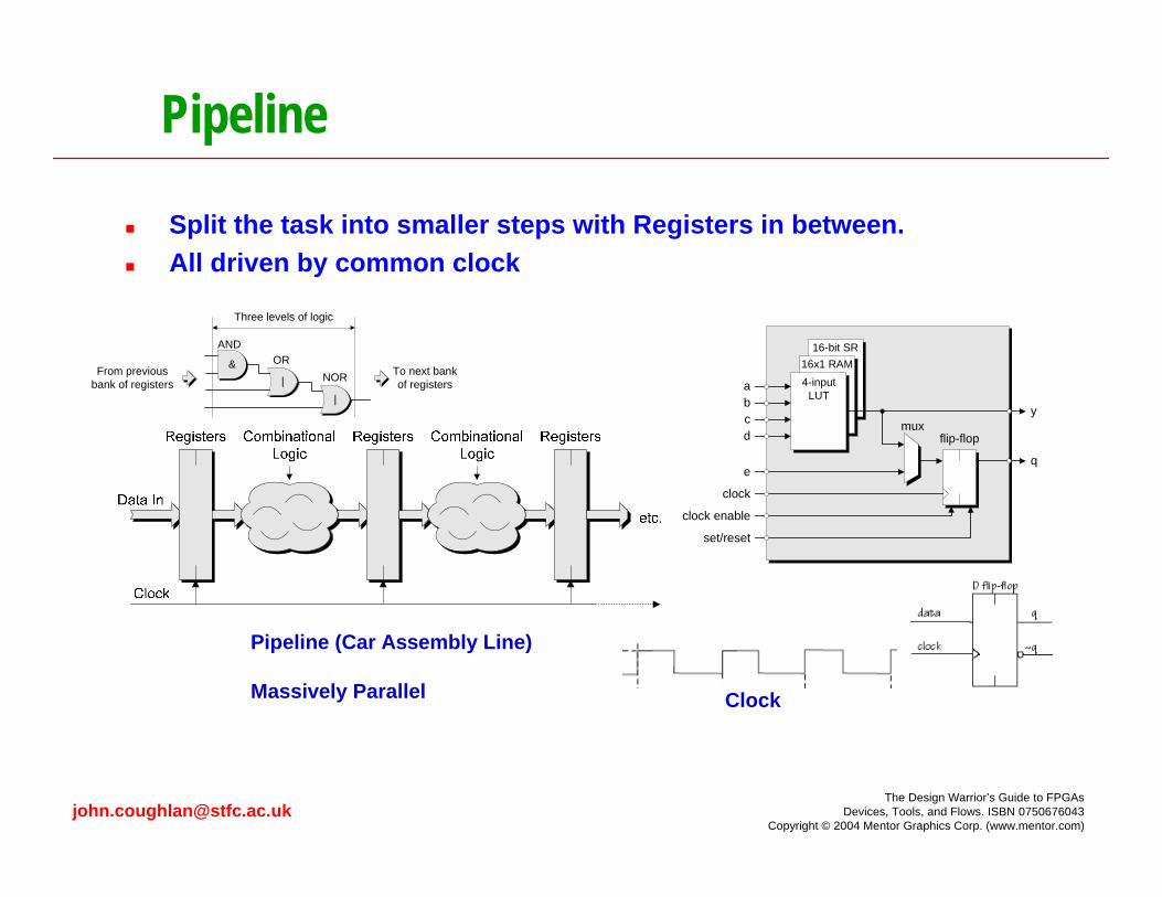
Pipeline
Split the task into smaller steps with Registers in between.All driven by common clock
16-bit SR
flip-flop
clock
muxy
qe
abcd
16x1 RAM4-input
LUT
clock enable
set/reset
Clock
Pipeline (Car Assembly Line)
Massively Parallel
&|
ANDOR
|
NORFrom previousbank of registers
To next bankof registers
Three levels of logic
[email protected] Design Warrior’s Guide to FPGAs
Devices, Tools, and Flows. ISBN 0750676043Copyright © 2004 Mentor Graphics Corp. (www.mentor.com)
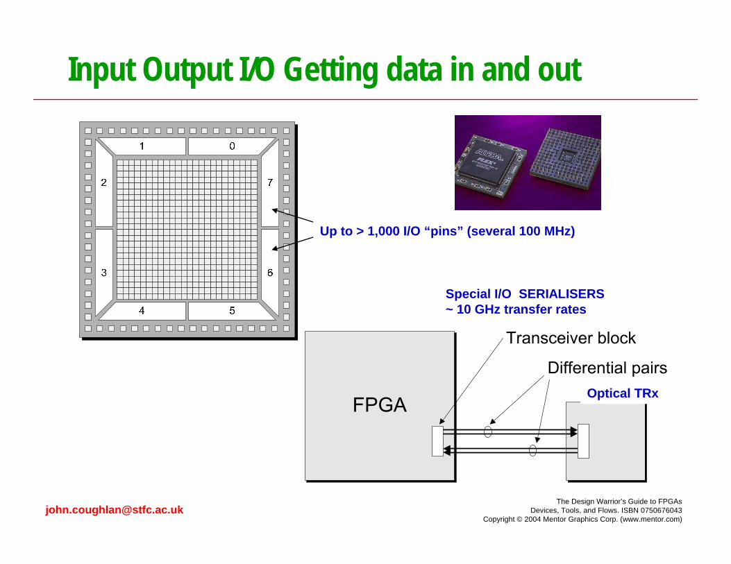
Input Output I/O Getting data in and out
Up to > 1,000 I/O “pins” (several 100 MHz)
Special I/O SERIALISERS~ 10 GHz transfer rates
Optical TRx
[email protected] Design Warrior’s Guide to FPGAs
Devices, Tools, and Flows. ISBN 0750676043Copyright © 2004 Mentor Graphics Corp. (www.mentor.com)
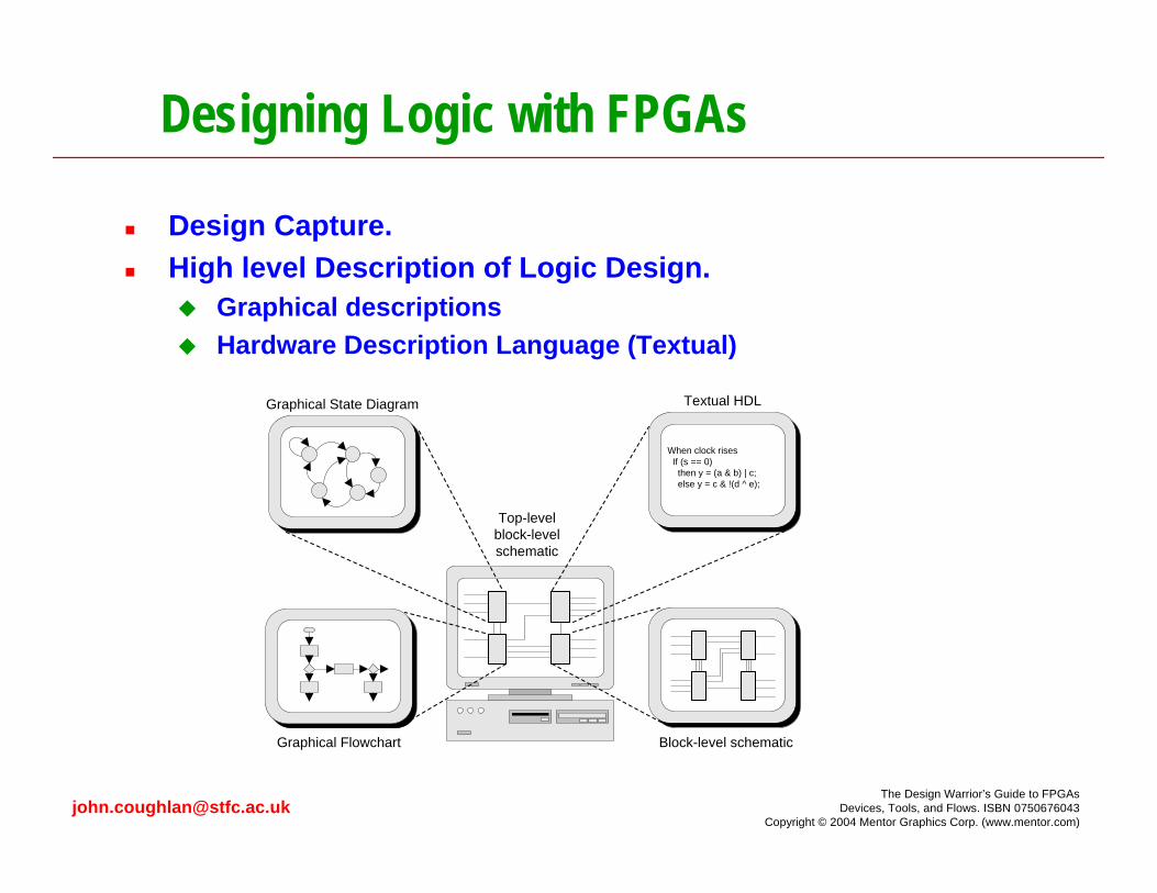
Designing Logic with FPGAs
Design Capture. High level Description of Logic Design.
Graphical descriptionsHardware Description Language (Textual)
Graphical State Diagram
Graphical Flowchart
When clock rises If (s == 0) then y = (a & b) | c; else y = c & !(d ^ e);
Textual HDL
Top-levelblock-levelschematic
Block-level schematic
[email protected] Design Warrior’s Guide to FPGAs
Devices, Tools, and Flows. ISBN 0750676043Copyright © 2004 Mentor Graphics Corp. (www.mentor.com)
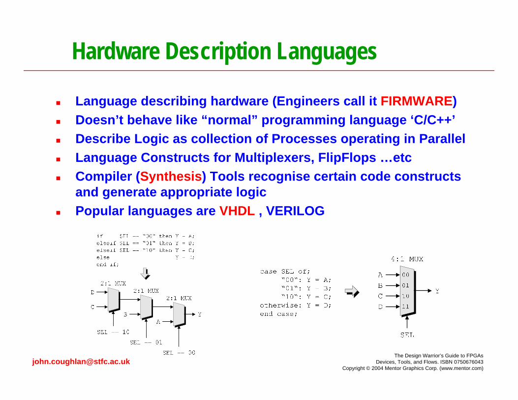
Hardware Description Languages
Language describing hardware (Engineers call it FIRMWARE)Doesn’t behave like “normal” programming language ‘C/C++’Describe Logic as collection of Processes operating in ParallelLanguage Constructs for Multiplexers, FlipFlops …etcCompiler (Synthesis) Tools recognise certain code constructs and generate appropriate logicPopular languages are VHDL , VERILOG
[email protected] Design Warrior’s Guide to FPGAs
Devices, Tools, and Flows. ISBN 0750676043Copyright © 2004 Mentor Graphics Corp. (www.mentor.com)
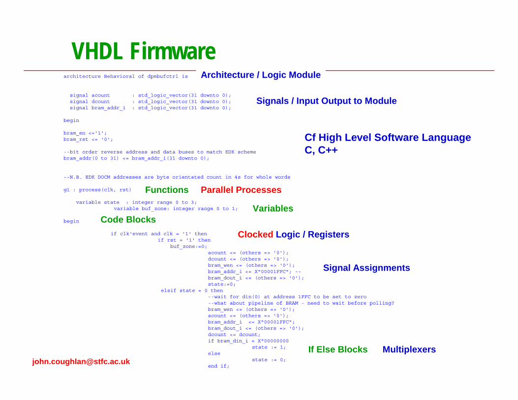
architecture Behavioral of dpmbufctrl is
signal acount : std_logic_vector(31 downto 0);signal dcount : std_logic_vector(31 downto 0);signal bram_addr_i : std_logic_vector(31 downto 0);
begin
bram_en <='1';bram_rst <= '0';
--bit order reverse address and data buses to match EDK schemebram_addr(0 to 31) <= bram_addr_i(31 downto 0);
--N.B. EDK DOCM addresses are byte orientated count in 4s for whole words
g1 : process(clk, rst)
variable state : integer range 0 to 3;variable buf_zone: integer range 0 to 1;
begin
if clk'event and clk = '1' thenif rst = '1' then
buf_zone:=0;acount <= (others => '0');dcount <= (others => '0');bram_wen <= (others => '0');bram_addr_i <= X"00001FFC"; --bram_dout_i <= (others => '0');state:=0;
elsif state = 0 then--wait for din(0) at address 1FFC to be set to zero--what about pipeline of BRAM - need to wait before polling?bram_wen <= (others => '0');acount <= (others => '0');bram_addr_i <= X"00001FFC";bram_dout_i <= (others => '0');dcount <= dcount;if bram_din_i = X"00000000" then
state := 1; else
state := 0;end if;
VHDL Firmware
Signals / Input Output to Module
Parallel Processes
Clocked Logic / Registers
If Else Blocks
Variables
Signal Assignments
Architecture / Logic Module
Cf High Level Software LanguageC, C++
Code Blocks
Functions
Multiplexers
[email protected] Design Warrior’s Guide to FPGAs
Devices, Tools, and Flows. ISBN 0750676043Copyright © 2004 Mentor Graphics Corp. (www.mentor.com)
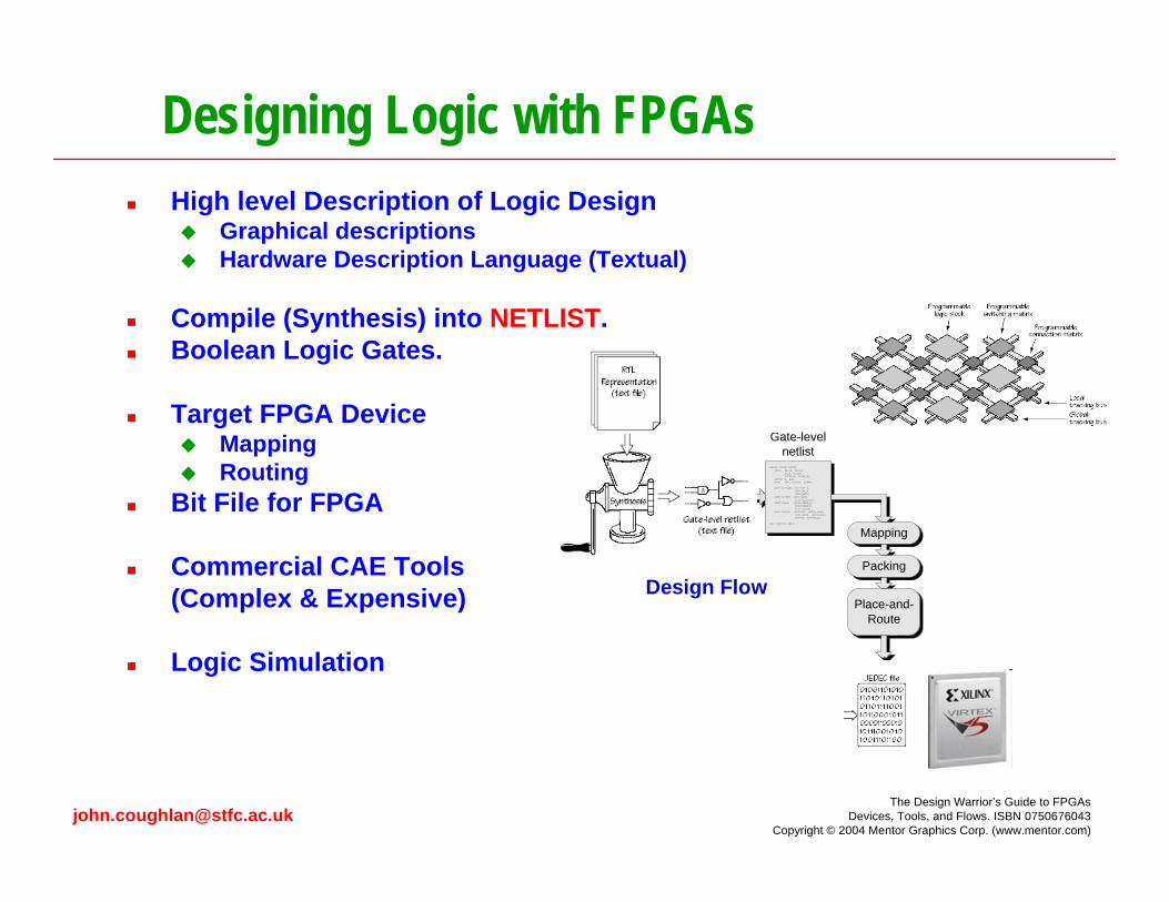
Designing Logic with FPGAsHigh level Description of Logic Design
Graphical descriptionsHardware Description Language (Textual)
Compile (Synthesis) into NETLIST. Boolean Logic Gates.
Target FPGA Device MappingRouting
Bit File for FPGA
Commercial CAE Tools(Complex & Expensive)
Logic Simulation
Gate-levelnetlist
BEGIN CIRCUIT=TEST INPUT SET_A, SET-B, DATA, CLOCK, CLEAR_A, CLEAR_B; OUTPUT Q, N_Q; WIRE SET, N_DATA, CLEAR;
GATE G1=NAND (IN1=SET_A, IN2=SET_B, OUT1=SET); GATE G2=NOT (IN1=DATA, OUT1=N_DATA); GATE G3=OR (IN1=CLEAR_A, IN2=CLEAR_B, OUT1=CLEAR); GATE G4=DFF (IN1=SET, IN2=N_DATA, IN3=CLOCK, IN4=CLEAR, OUT1=Q, OUT2=N_Q);
END CIRCUIT=TEST;
Fully-routed physical(CLB-level) netlist
Schematiccapture
Mapping
Packing
Place-and-Route Timing analysis
and timing report
Gate-level netlistfor simulation
SDF (timing info)for simulation
Design Flow
[email protected] Design Warrior’s Guide to FPGAs
Devices, Tools, and Flows. ISBN 0750676043Copyright © 2004 Mentor Graphics Corp. (www.mentor.com)
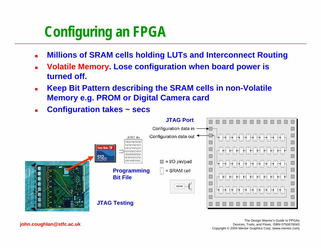
Configuring an FPGAMillions of SRAM cells holding LUTs and Interconnect RoutingVolatile Memory. Lose configuration when board power is turned off.Keep Bit Pattern describing the SRAM cells in non-Volatile Memory e.g. PROM or Digital Camera cardConfiguration takes ~ secs
JTAG Testing
JTAG Port
ProgrammingBit File
[email protected] Design Warrior’s Guide to FPGAs
Devices, Tools, and Flows. ISBN 0750676043Copyright © 2004 Mentor Graphics Corp. (www.mentor.com)
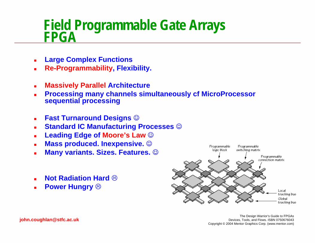
Field Programmable Gate Arrays FPGALarge Complex FunctionsRe-Programmability, Flexibility.
Massively Parallel ArchitectureProcessing many channels simultaneously cf MicroProcessorsequential processing
Fast Turnaround Designs ☺Standard IC Manufacturing Processes ☺Leading Edge of Moore’s Law ☺Mass produced. Inexpensive. ☺Many variants. Sizes. Features. ☺
Not Radiation Hard Power Hungry
[email protected] Design Warrior’s Guide to FPGAs
Devices, Tools, and Flows. ISBN 0750676043Copyright © 2004 Mentor Graphics Corp. (www.mentor.com)
FPGA Trends
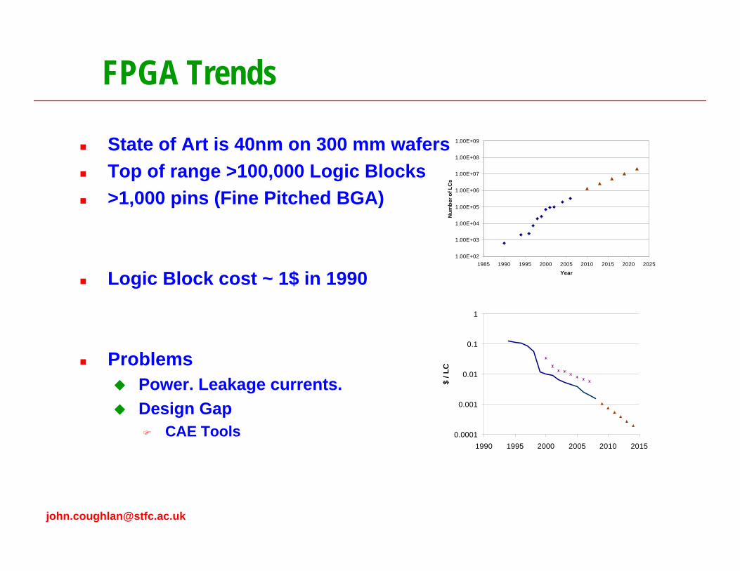
State of Art is 40nm on 300 mm wafersTop of range >100,000 Logic Blocks >1,000 pins (Fine Pitched BGA)
Logic Block cost ~ 1$ in 1990
ProblemsPower. Leakage currents. Design Gap
CAE Tools 0.0001
0.001
0.01
0.1
1
1990 1995 2000 2005 2010 2015$
/ LC
1.00E+02
1.00E+03
1.00E+04
1.00E+05
1.00E+06
1.00E+07
1.00E+08
1.00E+09
1985 1990 1995 2000 2005 2010 2015 2020 2025Year
Num
ber o
f LC
s
[email protected] Design Warrior’s Guide to FPGAs
Devices, Tools, and Flows. ISBN 0750676043Copyright © 2004 Mentor Graphics Corp. (www.mentor.com)
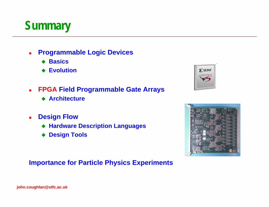
Summary
Programmable Logic DevicesBasicsEvolution
FPGA Field Programmable Gate ArraysArchitecture
Design FlowHardware Description LanguagesDesign Tools
Importance for Particle Physics Experiments