Embed Size (px)
Citation preview
Processor ICPSC 321
Andreas Klappenecker

Midterm 1
• Thursday, October 7, during the regular class time
• Covers all material up to that point• History• MIPS assembly language programming• Computer arithmetic• MIPS architecture
• Review on Tuesday, October 5

Administrative Issues
• Allen Parish will not have a help session this Friday, but again in subsequent Fridays.
• I will have extra office-hours this Friday, 10:30am-11:30am.
• There will be no office hours on Tuesday morning (PhD defense).

Questions? Problems?

Today’s Menu
The Processor: Datapath and Control
The Processor: Datapath and Control
We want to implement portions of MIPS• memory-reference instructions: lw, sw
• arithmetic-logical instructions: add, sub, and, or, slt• control flow instructions: beq, j
We ignore multiply, divide, and other integer and floating point instructions.
• Instruction Fetch• Instruction Decode and Register Fetch• Execution, Memory Address Computation, or
Branch Completion• Memory Access or R-type instruction
completion• Write-back step
Five Execution Steps

Implementations
All right, give us the details if you can’t
help it!
1) Fetch Instructions
• A memory unit is used to hold and supply the instructions given an address
• A state element, called the program counter, determines the address
• We need an adder to increment the program counter to the address of the next instruction.

2) Decode Instructions & Fetch Registers
Premise: We do not know at this point which instruction we ought to execute. BUT, we can do some speculative executions: • We can fetch the registers using the bits
21-25 and 16-20 of the instruction• Which instructions do not need this information? • The branch command uses bits 0-15 of the instruction (=> sign-extend to 32 bits).

Instruction Word Formats
• Register format
• Immediate format
• Jump format
0 rs rt rd shamt funct 0 rs rt rd shamt funct
op-code rs rt immediate valueop-code rs rt immediate value
op-code 26 bit current segment addressop-code 26 bit current segment address
6 5 5 16
6 5 5 5 5 6
6 26

3) Execution, Address Calculation, or Branch Completion
• Execution (depending on instruction) • compute a memory address (lw and sw)• compute an arithmetic result (int ops)• compare (for a branch) and set PC to
appropriate addressThe content of the registers are used as an input to the arithmetic-logic unit. The instruction decode sets the appropriate control signals.

Role of the ALU
The output of the arithmetic logic unit is• written to a register in the case of
arithmetic-logical instructions• used as an address in the case of load
and store instructions• used to determine the next instruction
address for branch instructionsThe ALU has a great variety of roles!

4) Memory Access or R-Type Instruction Completion
For load and store instructions, the address ALU_Out calculated by the arithmetic-logic unit is used for memory reference: • read MDR = Mem[ALUOut] or• store Mem[ALUOut] = BFor arithmetic-logical instructions, write the result of the operation into the destination register
(Actually, this is the description for the multi-cycle processor)

5) Write-Back
Load instructions complete by writing back the value from the memory.
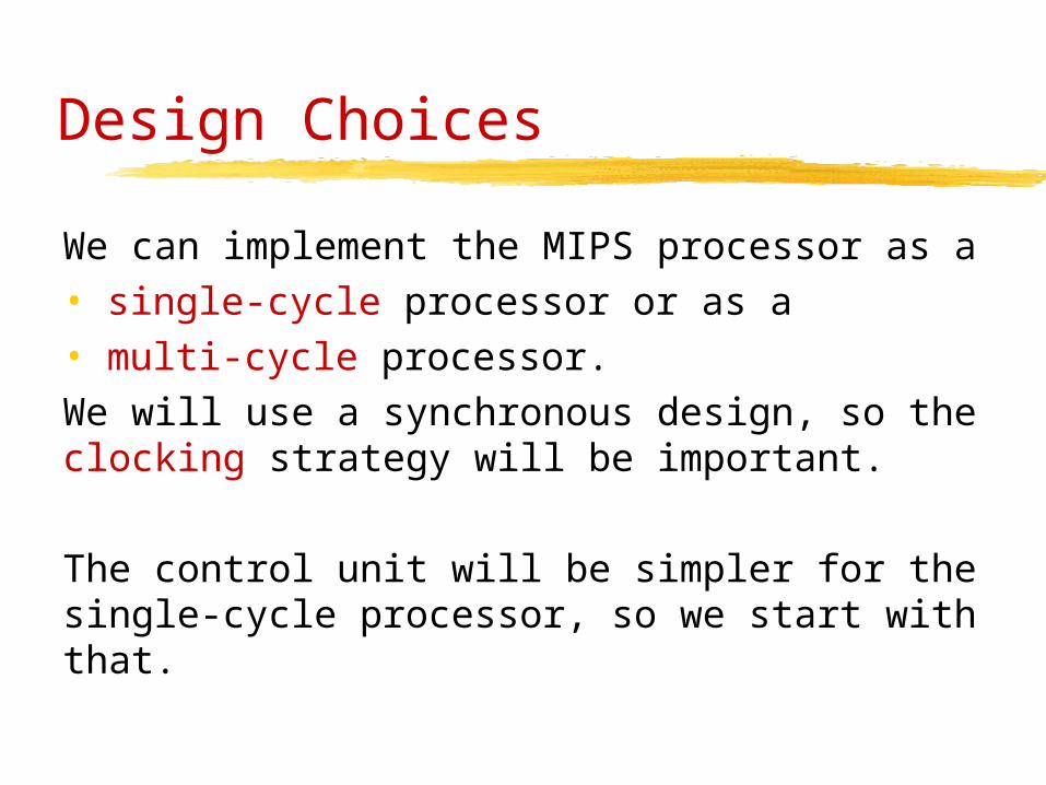
Design Choices
We can implement the MIPS processor as a• single-cycle processor or as a • multi-cycle processor.We will use a synchronous design, so the clocking strategy will be important.
The control unit will be simpler for the single-cycle processor, so we start with that.

• Abstract, simplified view
• Two types of functional units:• elements that operate on data values (combinational)• elements that contain state (sequential)
Simplified Datapath
Registers
Register #
Data
Register #
Datamemory
Address
Data
Register #
PC Instruction ALU
Instructionmemory
Address

Combinatorial and Sequential Elements
• The ALU is a combinatorial element• Other elements of the design are not
combinatorial, but contain a state• An element with some internal storage
is called a state element• State elements have at least two inputs:
• data• clock (determines when data is written)

Clocking Methodology
• We need to decide when signals can be read and written
• We need to specify timing behavior• For simplicity, we assume an edge-triggered
clocking strategy (synchronous design)• All storage elements are updated on either
raising edge or falling edge:
cycle timerising edge
falling edge
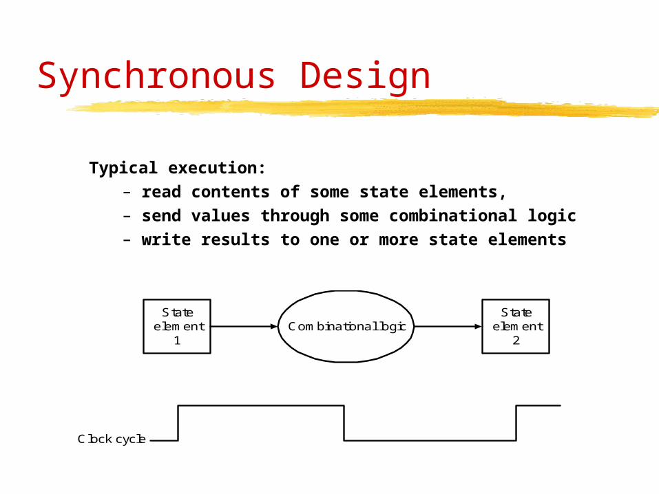
Synchronous Design
Clock cycle
Stateelement
1Combinational logic
Stateelement
2
Typical execution:– read contents of some state elements, – send values through some combinational logic– write results to one or more state elements
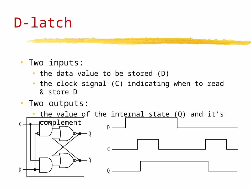
• Two inputs:• the data value to be stored (D)• the clock signal (C) indicating when to read & store D
• Two outputs:• the value of the internal state (Q) and it's
complement
D-latch
Q
C
D
_Q
D
C
Q
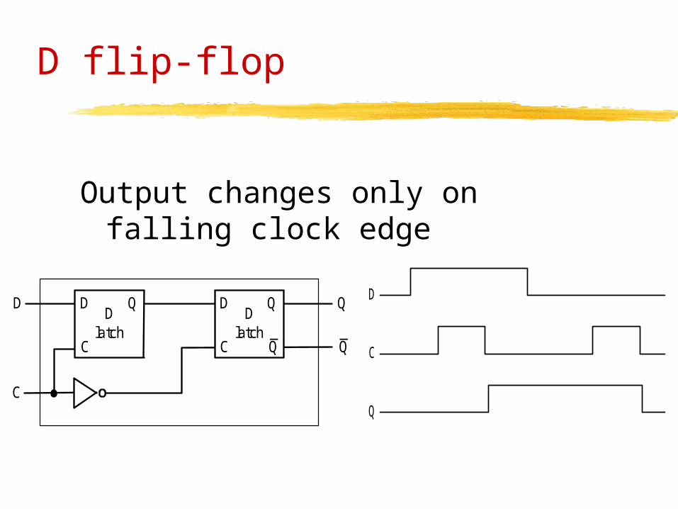
D flip-flop
Output changes only on falling clock edge
_Q
Q
_Q
Dlatch
D
C
Dlatch
DD
C
C
D
C
Q
Summary
• We will use D-flip flops to build the register file
• We gradually build up the datapath
• Simple components will allow us to do this
• We add the control logic a little later
• You will need a firm understanding of logic design
• Study Chapter 4, read Appendix B

Instruction Fetch
PC
Instructionmemory
Instructionaddress
Instruction
a. Instruction memory b. Program counter
Add Sum
c. Adder
• Use PC to find new instruction
• PC = PC + 4, preparing for next instruction

Instruction Fetch + PC update

R-Format Instructions
• Register format
• op: basic operation of instruction• funct: variant of instruction• rs: first register source operand• rt: second register source operand• rd: register destination operand• shamt: shift amount
op-code rs rt rd shamt functop-code rs rt rd shamt funct
6 5 5 5 5 6
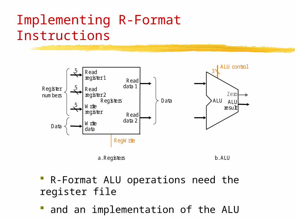
Implementing R-Format Instructions
ALU control
RegWrite
RegistersWriteregister
Readdata 1
Readdata 2
Readregister 1
Readregister 2
Writedata
ALUresult
ALU
Data
Data
Registernumbers
a. Registers b. ALU
Zero5
5
5 3
R-Format ALU operations need the register file
and an implementation of the ALU
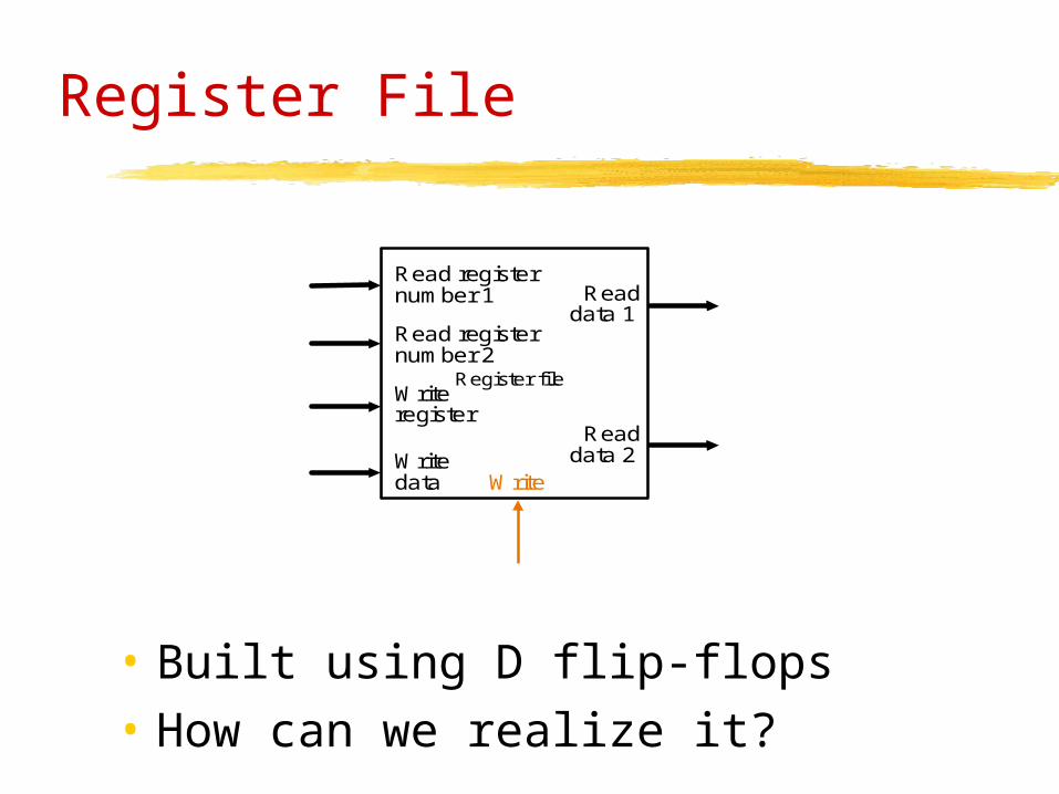
• Built using D flip-flops• How can we realize it?
Register File
Read registernumber 1 Read
data 1
Readdata 2
Read registernumber 2
Register fileWriteregister
Writedata Write

Reading the Register File
Mux
Register 0
Register 1
Register n – 1
Register n
Mux
Read data 1
Read data 2
Read registernumber 1
Read registernumber 2
Multiplexers select the outputs

D flip-flop
Output changes only on falling clock edge
_Q
Q
_Q
Dlatch
D
C
Dlatch
DD
C
C
D
C
Q

Writing into the Register File
• log n+1 input bits address n+1 registers
• Falling edge of clock signal determines when to write
n-to-1decoder
Register 0
Register 1
Register n – 1C
C
D
DRegister n
C
C
D
D
Register number
Write
Register data
0
1
n – 1
n

Implementing Loads and Stores
Register file, ALU, data memory unit, sign extension unit
16 32Sign
extend
b. Sign-extension unit
MemRead
MemWrite
Datamemory
Writedata
Readdata
a. Data memory unit
Address

Datapath for a load and store
1. register access 2. memory access calculation3. read or write from memory4. in the case of a load, write into register file
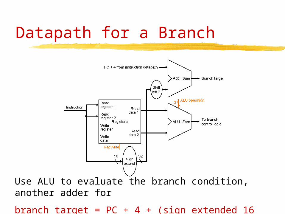
Datapath for a Branch
Use ALU to evaluate the branch condition, another adder for
branch target = PC + 4 + (sign extended 16 bits)>>2

Summary
• Found implementations for R-format instructions
• Found implementations for loads and stores
• Found implementations for branches
• We need to compose these datapaths
• Simplicity of the implementations is striking!

![CPSC 411 Design and Analysis of Algorithmsfaculty.cse.tamu.edu/klappi/csce411-f12/csce411-set10.pdf1 Graph Algorithms Andreas Klappenecker [based on slides by Prof. Welch] Monday,](https://img.dokumen.tips/doc/110x75/5aebbeff7f8b9ab24d8f2289/cpsc-411-design-and-analysis-of-graph-algorithms-andreas-klappenecker-based-on.jpg)