Embed Size (px)
Citation preview
483
Lattice Electron Microscopy and Image Processing of Ion-Implantedand Laser-Annealed GaAs Structures
Gianfranco Vitali(1), Marco Rossi(1), Giuseppe Zollo(1), Cesare Pizzuto(1),Nikolai Pashov(2) and Maria Kalitzova(2)
(1) Dipartimento di Energetica, Università "La Sapienza", via A. Scarpa, 14 - 00161 Roma and INFM,UdR RM I, Italy(2) Institute of Solid State Physics, Bulgarian Academy of Sciences, Tzarigradsko Chaussee, 72 -1784Sofia, Bulgaria
(Received March 1; accepted May 22, 1995)
Abstract. 2014 The efficiency of the Low-Power Pulsed-Laser Annealing (LPPLA) as a treatment torestore the ion implantation induced crystal disorder is well-known, but it is still open the question re-garding the way in which is possible to model the LPPLA dynamic effects. At this purpose we believethat a deeper knowledge about the modification of the ion-induced extended defects (dislocations,stacking faults, clusters), as a consequence of the LPPLA treatment, is relevant. In our opinion, atechnique suitable to gain this information could be the lattice image digital processing. In this paperwe reported the experimental results concerning the use of this technique applied to some HRTEMimages of low-dose implanted GaAs samples. In particular, the appearance of different types of ex-tended defects in the implanted material and their annealing with LPPLA have been put in evidence.
Microsc. Microanal. Microstruct.
Classification
Physics Abstracts61.72F - 81.40
1. Introduction
The main advantages of ion implantation as a technique to develop GaAs devices and integratedcircuits are well-established. The active channel formation in similar implanted substrates is be-lieved to be a key process in the high-speed electronic technology [1].The nature of the damage created in as-implanted substrates is important for the efficiency of
the next stages in the processing, because the extended defect structure, their diffusion and an-nealing affect in a strong way the electrical devices properties. In the ion implantation doping ofmaterials as GaAs, a large number of atoms (several thousand) are displaced in collision cascades,creating defects zones in the crystal lattice characterized by a vacancies core with a periphery richof interstitials [2]. What kind of point-defect clustering in such zinc-blend structure preferentiallydevelops, far from the thermodynamic equilibrium, is still an open question. For the case of FCCmetals, it seems now well-established that the microscopical processes occurring during the ionimplantation mainly induce the formation of edge dislocations and dislocation loops of interstitialand vacancy type in the cascade-volume [3]. Transmission electron microscopy (TEM) has been
Article available at http://mmm.edpsciences.org or http://dx.doi.org/10.1051/mmm:1995139
484
extensively used in the past to obtain direct information about the defect-zones produced by indi-vidual displacement cascades and about the in-depth radiation-damage distribution. In this wayTEM provides knowledge on the processes generating structural damage in the ion implantationof semiconducting materials.The possibility to perform the annealing of ion implanted GaAs, with the Low-Power Pulsed-
Laser treatment (LPPLA) at temperatures far below the dissociation temperature of the material[4-6], provides new aspects of interest for the Electron Microscopy, connected with the studyof very fine crystal structural details into the atomic structure of the damaged zones and theirevolution during the annealing. Comprehensive information about such characteristic structurescan been gained by additional digital processing of the obtained images [7]. This technique canfurnish a valid complementary investigation to the electrical measurements to evaluate the effectof the LPPLA.Thé damage produced by the ion implantation or the residual one detectable after the LPPLA,
together with the electron microscopy instabilities, give pictures characterized by particulars witha ratio between the signal and the noise (S/N) that can be very low. In the HRTEM of examinedspecimens, our interest is exactly directed to casual imperfections of the periodic structure asdefect clusters, dislocation loops, grain boundaries, interfaces etc.. As a consequence, the physicalsituation is particularly suitable for the image processing to improve the S/N ratio.
2. Experimental
Single crystal semi-insulating (100) GaAs wafers were implanted with 140 keV Zn+ ions, a fluenceof D = 1014 cm-2, at temperature T = 110 ± 10 ° C and random direction.The laser annealing has been performed in air and at room temperature by 30 successive super-
imposed pulses, at a frequency of 0.05 Hz, each of them with a density power Po = 4.5MWcm-2from a Q-switched ruby-laser (À = 694 nm) with a pulse duration 0394tFWHM = 25 ns.The above mentioned value of Po is lower than the optimal requested for annealing (ranging
between 5 and 6 MW cm-2) as already shown [4-6]. The calculated maximum temperature of thematerial (as described elsewhere [8]) in the present irradiation conditions does not exceed 700 K.The used annealing conditions, were expected to be characterized by well expressed stages of
the defects evolution.All the following reported HRTEM investigations, performed on as-implanted and LPPLA
treated samples, have been carried out by a 4000Ex-Jeol instrument operating at 400 kV in brightfield many-beam mode.The obtained HRTEM micrographs have been successively digitalized and processed in a Kon-
tron System in order to improve the signal to noise ratio S/N with a negligible loss of resolution.At this regard, one can suppose that a high resolution electron-microscopy image is obtained
as a resultant of three superimposed contributions:
i) a known periodic signal P(r) connected with the periodic crystal lattice potential;ii) an unknown signal X (r), that is the subject under study, not periodic but connected with theperiodic structure;iii) the noise N (r ) with a casual intensity and linked with the specimen or/and with the electron-microscopy instabilities. In a first approximation, the above mentioned contributions are additive,so that the intensity in any point of the picture is given by:
The filtered image in the spatial frequencies field will be:
485
where the filtering function F(g) will be chosen in order to minimize the product N(g)F(g) and,in the same time, to give maximum X (g)F(g). This choice is the criterion for the filter selection:this requirement corresponds to find the best balance between the contrast and/or the image reso-lution of the object under study. So the S/N ratio of the examined micrographs showing a periodicmotif, can be increased through the convolution provided by an optical filter consistent of circularapertures in the position of the optical diffraction spots (Bragg Filters).
3. Results and Discussions
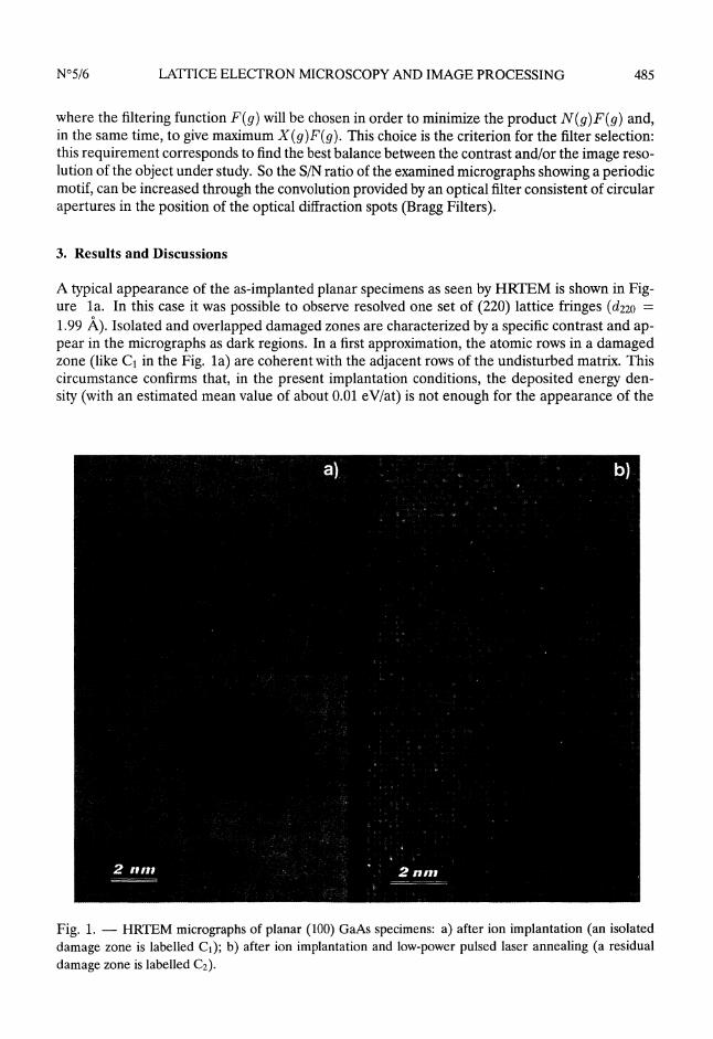
A typical appearance of the as-implanted planar specimens as seen by HRTEM is shown in Fig-ure la. In this case it was possible to observe resolved one set of (220) lattice fringes (d220 =1.99 À). Isolated and overlapped damaged zones are characterized by a specific contrast and ap-pear in the micrographs as dark regions. In a first approximation, the atomic rows in a damagedzone (like Ci in the Fig. la) are coherent with the adjacent rows of the undisturbed matrix. Thiscircumstance confirms that, in the present implantation conditions, the deposited energy den-sity (with an estimated mean value of about 0.01 eV/at) is not enough for the appearance of the
Fig. 1. - HRTEM micrographs of planar (100) GaAs specimens: a) after ion implantation (an isolateddamage zone is labelled Ci); b) after ion implantation and low-power pulsed laser annealing (a residualdamage zone is labelled C2).

486
Fig. 2. - Filtered image, with one pair of reflections corresponding to one set of (220) planes, of theisolated damage zone CI shown in Figure la. Edge dislocations (D), dislocation loops of interstitial (DLi)and vacancy (DLv) type are indicated.
amorphization within the displacement cascade, the reported critical energy density for the amor-phization being around 2.0 eV/at for irradiation at 300 K [9]. The ion-induced damage producedin such conditions is classified as "type 1 defects", i.e. defects forming with a dose exceeding a criti-cal dose necessary for the formation of extended defects but not sufficient to obtain an amorphouslayer [10]. In the present case, the distribution of type I detects has a maximum in correspondencewith the measured projected range (Rp about 85 nm), higher thàn the calculated one due to thetemperature enhanced diffusion of impurity and point defects [9].The main source of point defects for the damaged zones formation is the Frenkel pairs pro-
duction during the collision cascades phenomena. When the displacement events in the thermalspikes stop (i.e. the colliding atoms loose their energy) a spatial arrangement of Frenkel defectsforms with vacancies at the center and self-intèrstitials in the periphery that can organize them-selves in small edge dislocations or dislocation loops [11-13]. Moreover, the vacancy-rich core canrelax too and form vacancy clusters such as dislocation loops. In the present case, the elevatedtemperature implantation conditions can enhance the diffusion and the clustering of Frenkel pairsout of the collision cascade. The inner structure of the so formed damaged zones, as those named

487
Fig. 3. - Filtered image, with one pair of reflections corresponding to one set of (220) planes, of theisolated damage zone C2 shown in Figure Ib.
CI in Figure la, and their evolution under the LPPLA treatment could in principle be viewedthrough High Resolution Transmission Electron Microscopy but a poor S/N ratio can inhibit thispossibility. In order to obtain more precise information about the kind of localized periodicity dis-turbances in the images of the isolated damaged zones, they were digitally processed using Braggfilters in the Fourier space with one or two pairs of strong reflections.From the experimental results, it was concluded that an useful filter configuration was one using
a pair of strong reflections corresponding to one set of (220) resolved lattice planes. In this casethe reconstructed image of the analysed part of the crystal lattice projection was presented withan improved contrast for all periodicity disturbances.The filtered image of an isolated damaged zone of an as-implanted GaAs crystal, observed by
HRTEM in 100 > projection, is shown in the Figure 2. It clearly shows that the damagedregions contain a large number of extended lattice defects, mainly dislocation loops of vacancyand interstitial type (DLy or DLi in the Fig. 2) and edge dislocations (indicated with D). Thedistribution of the observable extended defects is not homogeneous with a calculated averagedensity of the order of 1013 cm-2.The effects of LPPLA treatment to recover the lattice order of the ion-implanted specimen, is
clearly visible in the obtained filtered image of residual damaged zones of an implanted and LP-PLA treated sample (C2 in the Fig. 1b) shown in Figure 3; the same filtering procedure describedabove has been applied.
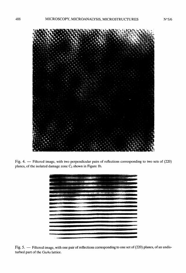
Moreover, a filtered image of the same damaged zone, generated using a Bragg filter with twopairs of strong reflections, is shown in Figure 4.From the filtered images of the damaged zones in LPPLA specimens, is clear that no extended
defects (as dislocation loops) are found in the examined zone and only very weak disturbances canbe detected: it is worth noting the efficiency of the applied LPPLA treatment in the recovering ofthe GaAs lattice crystallinity, compromised by ion implantation.
Only as a reference, a filtered image ôf an undisturbed part of an implanted sample is shownin the Figure 5. This picture was obtained in the same conditions of all above: the similarity withthat shown in the Figure 3 is evident.
488
Fig. 4. - Filtered image, with two perpendicular pairs of reflections corresponding to two sets of (220)planes, of the isolated damage zone C2 shown in Figure 1b.
Fig. 5. - Filtered image, with one pair of reflections corresponding to one set of (220) planes, of an undis-turbed part of the GaAs lattice.

489
4. Conclusions
As shown by processing of HRTEM micrographs, extended defects (vacancy and interstitial typedislocation loops and edge dislocations) form in damaged zones of as-implanted GaAs due to theclustering of point defects. The calculated density of these extended defects is of the order of1013 cm-2. The experimental data on the behaviour of different point or/and extended defects ina zinc-blend structure are very scarce.
From the above reported results, we can conclude that, at the used implantation conditions,point defects created in the displacement cascades tend to cluster forming small DLs.
By the way one can observe that this effect shows some analogy with the behaviour of FCCmetals like Cu and Ni under irradiation with MeV protons, neutrons and heavy ions [14, 15].In this case, by combined TEM and computer simulation, it has been demonstrated that self-interstitial atoms (SIA) are clustering efficiently in energetic collision cascades [16]. Computersimulations of the behaviour of SIA-type dislocation loops in FCC metals indicate that at leastthe smaller ones are rather mobile. Thermally activated changes of the Burgers vectors of thesedefect structures in crystallographic equivalent directions result in a zig-zag motion of the DLs inthe crystal lattice [16].
In the present case related to a zinc-blend compound semiconductor, the above reported HR-TEM observations and previous HVTEM investigations [17], indicate that the LPPLA effectsshould be connected with the extended defects (both V and SIA types) migration induced by theabsorbed laser energy. In fact, the "solid phase epitaxy" occurring in the laser annealed speci-mens, is related (in the authors’ opinion) to the bonds weakening of the defect atoms which areionized during the laser energy absorption process [6]. The laser induced extended defects migra-tion, results in their accumulation in "defects lines" (high density defects alignments) parallel tothe (110) planes as it was shown by HVTEM [17]. It is worth to notice that all the above discusseddata, concerning the type, the concentration and the restoration degree of extended lattice defectsin GaAs, are related only to the behaviour of isolated defect zones embedded in an undisturbedmatrix in the case of a low-dose implantation (1014 cm-2). In order to put in evidence the qualityof the restored structure treated with the LPPLA, the similarity between the filtered image fromthe undisturbed matrix region of as-implanted samples (Fig. 5) and that from a defect zone afterthe LPPLA treatment (Fig. 3) must be underlined. The undisturbed matrix shown in Figure 5puts in evidence, as a peculiarity of low-dose ion-bombarded structures, the inhomogeneity of theinduced damage. The last one is the indispensable condition for the LPPLA and the consequentepitaxy.
In the case of overlapping defect zones, the situation is much more complicated and will not bediscussed in this paper.
The calculated temperature T of the GaAs surface during LPPLA [8], does not exceed 700 K.In this condition, the behavior of the LPPLA GaAs samples seems homologous to the behaviorshown in the non-equilibrium-phase-diagram for Ni proposed by Jaeger et al. [14]. In this diagram,the appearance of periodic defect cluster arrangements parallel to (100) planes, in the case ofneutrons, protons and heavy ions irradiation, is indicated to occur for T = 0.35 Tm, being Tm themelting temperature [14, 15].As an open question remains the exact modelling of the LPPLA dynamical effects in the 111-V
compound semiconductor. Furthermore it is interesting to note that a standard thermal annealingof GaAs, at temperatures at which the LPPLA provokes an effective rearrangement of the defectclusters, has only a very restricted influence on the defect structures of ion implanted GaAs [18].
490
Acknowledgements
The investigations shown in the present paper have been carried out within the frames of thescientific agreement between the Italian CNR and the Bulgarian Academy of Sciences.
References
[1] Graf V, Heuberger W, Nucl. Instr. Meth. B 19/20 (1987) 388.[2] Kalitzova M., Pashov N., Vitali G. and Rossi M., Mat. Res. Soc. Symp. Proc. 128 (1989) 683.[3] Jager W., Trinkaus H., J. Nucl. Mater 205 (1993) 349.
[4] Vitali G., Rossi M., Karpuzov D., Budinov H., Kalitzova M., Katardjiev I., Nucl. Instr. Meth. Res. Phys.B 59/60 (1991) 1077.
[5] Vitali G., Jpn. J. Appl. Phys. 31 (1992) 2049.[6] Vitali G., Pizzuto C., Rossi M., Zollo G., Karpuzov D., Kalitzova M., Jpn. J. Appl. Phys. 33 (1994) 2762.[7] De Jong A.F., Coene W., Van Dyck D., Ultramicrosc. 27 (1989) 53.
[8] Zollo G., Palumbo L., Rossi M., Vitali G., Appl. Phys. A 56(1993) 409.
[9] Kalitzova M., Karpuzov D., Pashov N., Vitali G., Rossi M. and Scholtz R., Nucl. Instr. Meth. Phys. Res.B80/81 (1993) 647.
[10] Jones K.S., Rozgonyi G.A., Rapid Thermal Processing Science and Technology (Academic Press, 1993)p. 123.
[11] Jager W, Trinkaus H., J. Nucl. Mat. 205 (1993) 394.
[12] Von Guerard B., Grasse D. and Peisl J., Phys. Rev. Lett. 44 (1980) 262.
[13] Rauch R., Peisl J., Schmalzbauer A. and Wallner G., J. Nucl. Mater. 168 (1989) 101.[14] Jager W., Ehrhart P., Shilling W., Solid State Phenomena 3/4 (1988) 279.
[15] Trinkaus H., Jager W, IFF Bulletin 41 (1992) 2.
[16] Jager W., Trinkaus H., Mater. Sci. Forum 123-125 (1993) 661.
[17] Pashov N., Kalitzova M., Vitali G., Rossi M. and Baither D., Jpn. J. Appl. Phys. 32 (1993) 2597.
[18] Morgen D.V, Eissen F.H., in Gallium Arsenide, Materials, Devices and Circuits (John Wiley & Sons,1985) p. 163.