Embed Size (px)
Citation preview

Field Ion Microscopy for theCharacterization of Scanning Probes 5William Paul and Peter Gr€utter
Contents
1 Definition of the Topic . . . . . . . . . . . . . . . . . . . . . . . . . . . . . . . . . . . . . . . . . . . . . . . . . . . . . . . . . . . . . . . . . . . . . . 160
2 Overview . . . . . . . . . . . . . . . . . . . . . . . . . . . . . . . . . . . . . . . . . . . . . . . . . . . . . . . . . . . . . . . . . . . . . . . . . . . . . . . . . . . . 160
3 Field Ion Microscopy for the Characterization of Scanning Probes . . . . . . . . . . . . . . . . . . . . . . 161
3.1 Introduction . . . . . . . . . . . . . . . . . . . . . . . . . . . . . . . . . . . . . . . . . . . . . . . . . . . . . . . . . . . . . . . . . . . . . . . . . . . 161
3.2 Experimental and Instrumental Methodology . . . . . . . . . . . . . . . . . . . . . . . . . . . . . . . . . . . . . . . 164
3.3 Key Research Findings . . . . . . . . . . . . . . . . . . . . . . . . . . . . . . . . . . . . . . . . . . . . . . . . . . . . . . . . . . . . . . . 182
3.4 Conclusions and Future Perspective . . . . . . . . . . . . . . . . . . . . . . . . . . . . . . . . . . . . . . . . . . . . . . . . . . 192
References . . . . . . . . . . . . . . . . . . . . . . . . . . . . . . . . . . . . . . . . . . . . . . . . . . . . . . . . . . . . . . . . . . . . . . . . . . . . . . . . . . . . . . . 193
Abstract
Scanning probe microscopy (SPM) is a widely used tool for investigating the
nanoscale structure of materials, as well as their electronic and mechanical
properties with its related spectroscopic modes of operation. In SPM experiments,
the sharp tip which probes the material under investigation is usually
uncharacterized; however, its geometry and chemical composition play a large
role in the SPM’s lateral imaging resolution and the features recorded in electronic
and force spectroscopies. To carry out comparisons with modeling, one must
consider a set of plausible tip structures and choose the one which best reproduces
the experimental data recorded with the uncharacterized tip.
With an atomically defined tip prepared by FIM, the electronic and mechanical
properties of the SPM probe are predetermined before the experiment, permitting
W. Paul (*)
IBM Research Division, Almaden Research Center, San Jose, CA, USA
e-mail: [email protected]
P. Gr€utterPhysics Department, McGill University, Montreal, QC, Canada
# Springer-Verlag Berlin Heidelberg 2015
C.S.S.R. Kumar (ed.), Surface Science Tools for Nanomaterials Characterization,DOI 10.1007/978-3-662-44551-8_5
159
direct comparison with theory, as well as the quantitative determination of
parameters which depend on tip radius, such as stresses during indentation.
Here we describe the implementation of FIM for the characterization of
scanning probe apices. This includes topics of tip integrity, characterization,
advanced preparation methodologies, and key research findings from experi-
ments which combine FIM and SPM techniques.
Keywords
Field ion microscopy (FIM) • Scanning probe microscopy (SPM) • Scanning
tunneling microscopy (STM) • Atomic force microscopy (AFM) • Field
emission • Single-atom tips • Tip characterization • Nanoelectronics •
Nanomechanics
1 Definition of the Topic
The field ion microscope (FIM) can image the atomic structure of sharp metal tips
with nanometer-sized radii and is notable as being the earliest technique to produce
atomically resolved images of matter in real space. Using FIM, one can atomically
characterize, and even engineer, the sharp tips used in scanning probe microscopy
(SPM). In this chapter, we address the technical aspects of implementing these tips
in SPM experiments and review their application to scanning tunneling microscopy
(STM), atomic forcemicroscopy (AFM), and SPM-based nanoindentation experiments.
2 Overview
Scanning probe microscopy (SPM) is a widely used tool for investigating the
nanoscale structure of materials, as well as their electronic and mechanical prop-
erties with its related spectroscopic modes of operation. In SPM experiments, the
sharp tip which probes the material under investigation is usually uncharacterized;
however, its geometry and chemical composition play a large role in the SPM’s
lateral imaging resolution and the features recorded in electronic and force spec-
troscopies. To carry out comparisons with modeling, one must consider a set of
plausible tip structures and choose the one which best reproduces the experimental
data recorded with the uncharacterized tip.
With an atomically defined tip prepared by FIM, the electronic and mechanical
properties of the SPM probe are predetermined before the experiment, permitting
direct comparison with theory, as well as the quantitative determination of param-
eters which depend on tip radius, such as stresses during indentation.
Here we describe the implementation of FIM for the characterization of scanning
probe apices. This includes topics of tip integrity, characterization, advanced
preparation methodologies, and key research findings from experiments which
combine FIM and SPM techniques.
160 W. Paul and P. Gr€utter

3 Field Ion Microscopy for the Characterization ofScanning Probes
3.1 Introduction
The utility of the FIM for preparing and characterizing tips destined for SPM
experiments was considered by Hans-Werner Fink of IBM Z€urich in the context
of STM shortly after its invention [1]. The main advantage of an atomically defined
tip apex is that if the exact atomic arrangement of the apex is known, the electronic
structure of the tip and the lateral resolution of the STM are predetermined.
The same detailed knowledge of the apex termination, as well as the tip radius, is
useful for atomic force microscopy (AFM) experiments and important in the
interpretation of results from combined STM and AFM experiments.
Largely unknown, the atomic-scale tip structure is directly responsible for image
contrast [2, 3], as well as the details of the measured electronic properties by scanning
tunneling spectroscopy [4, 5], chemical bonding forces by force spectroscopy [6, 7],
and yield point of materials by indentation [8, 9]. In order to obtain quantitative and
reproducible data, which could be considered as a benchmark for computational
simulations, one requires a tip with known atomic structure. For example, FIM-
characterized tips could act as atomically defined electrodes to build junctions to
single molecules, where transport properties are sensitive to the atomic arrangement
of the contact electrodes [10].
One must first sort out the technical challenges surrounding the experiment, starting
with the reliable transfer of an atomically defined FIM tip to an SPM experiment: this
involves moving the tip and sample from an initial separation of the order of meters to a
working distance of some angstroms in a brief period of time and without crashing one
into the other. Many questions need to be addressed concerning the implementation of
FIM tips in SPM: Will the atomically defined tip be modified by impurities in the FIM
imaging gas? If so, can this be avoided? Although UHV is very clean, it still has a finite
rest gas pressure – how longwill the atomically defined tip remain atomically defined in
vacuum? How much time do we have to perform our atomically defined SPM exper-
iment? How can we approach the tip to the sample and ensure that it doesn’t crash or
become modified upon interaction with the substrate?
This chapter begins with a brief introduction to FIM and SPM, and then in Sect.
3.2, we focus on the experimental methodologies of FIM which are most relevant to
the characterization of SPM tips. Section 3.3 reviews research findings from STM,
AFM, and nanoindentation experiments with atomically defined probes.
3.1.1 Field Ion Microscopy (FIM)The field ion microscope was invented in 1951 by Erwin W. M€uller [11] and by 1956had achieved the first real-space images of matter with atomic resolution. The first
FIM images were of the atomic arrangement of the apex of very sharp tungsten
needles. By 1957, the surfaces of other refractory metals had also been imaged [12].
Although the atomic resolution of FIM is no longer unique among microscopes
5 Field Ion Microscopy for the Characterization of Scanning Probes 161

(TEM, SEM, STM, and AFM have all demonstrated atomic spatial resolution), there
still exist distinctive experimental applications of FIM. Particularly well suited to FIM
is the study of diffusion of single atoms or clusters on crystal surfaces, and this
technique has generated most of the existing experimental data about the diffusion of
atoms and clusters on metal surfaces [13].
Another unique feature of the FIM is the possibility of integrating a time-of-flight
(ToF) mass spectrometer to enable chemical analysis with single-atom sensitivity and
a spatial resolution of several angstroms. The combined technique is known as atom
probe field ion microscopy (AP-FIM) or more simply as the atom probe [14–17].
In AP-FIM, a pulsed field is applied to the FIM specimen to field evaporate a small
amount of material from its surface to be chemically analyzed in the ToF unit; it is a
destructive technique, consuming the sample as data is collected. Tien T. Tsong, a
colleague of M€uller’s from the beginning of FIM, wrote in his book on AP-FIM [12]
that the technique provides the “ultimate sensitivity in chemical analysis” because of
its exquisite single-atom sensitivity.1 Unlike scanning probe methods, AP-FIM can
access the chemical composition in the bulk of samples, and technique development
remains very active today in the computational reconstruction of the data into 3D
element-specific atomic maps. Applications of AP-FIM include the investigation of
chemical segregation of elements at crystalline defects (steels and semiconductors),
local studies of grain boundaries in nanocrystalline materials (with grains too small
for techniques like electron backscatter diffraction (EBSD) [20]), and short-range
order in materials (e.g., in high-temperature superconductors).
3.1.2 Scanning Probe MicroscopyScanning probe microscopy uses a physical probe to image surfaces by raster scanning
the surface and monitoring some type of interaction between the probe’s apex and the
sample. In STM, a small current tunneling between the tip and the sample, on the order
of pA to nA, is used as an imaging mechanism [21–23]. Due to the current’s
exponential dependence on the tip-sample distance, with one decade of variation per
angstrom, excellent spatial resolution is possible. In AFM, the force or force gradient
between the tip and sample is responsible for image contrast [24, 25]. Electrostatic,
van derWaals, and chemical bonding forces all contribute to the force-distance profile,
so the AFM’s resolution depends on which particular force interaction is dominant.
STM and AFM are usually operated under feedback to maintain either constant
current or force (or force gradient) while the tip scans the surface. This procedure
traces out an isosurface of constant tip-sample interaction, often termed the “topog-
raphy” of the sample. In particularly stable instruments, often at cryogenic
1We note that single-atom chemical sensitivity has also been achieved recently in STM and AFM
techniques: inelastic electron tunneling spectroscopy in STM allows for measurement of the
vibrational energies of individual chemical bonds, which is a form of chemical sensitivity – for
example one can distinguish between hydrogen and deuterium bonds [18, 19]. In the case of AFM,
however, it is more of a relative chemical sensitivity obtained by comparing force-distance
interaction curves from different atomic species with the same tip. Absolute chemical identifica-
tion relies on the specifics of the tip apex which is usually unknown [6].
162 W. Paul and P. Gr€utter
temperatures, a constant height scan over the sample can be performed while the
variations of current or force are recorded as a function of tip position, forming an
“image” of these interactions. SPM can also be used to perform spectroscopy, in
which one parameter is modified and the response of another is measured, such as
force versus distance, current versus voltage, etc.
In all SPM experiments, the tip structure has a crucial role in contrast formation
and data interpretation. Surface science has progressed to the point where the SPM
community is able to study exquisitely well-defined surfaces, but the tip of the SPM
remains mostly uncharacterized – often one must turn to atomistic modeling to
guess at possible structures [7, 26]. Exceedingly few SPMs exist with in situ tip
characterization facilities – in this chapter, we consider FIM as a characterization
tool for the sharp SPM tips.
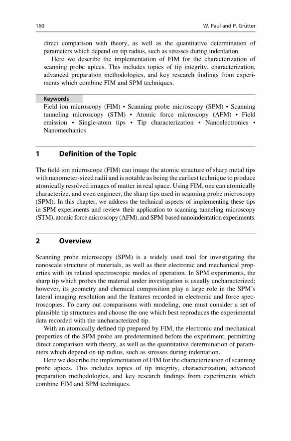
3.1.3 Combined STM/AFM/FIMAs an example of an apparatus which combines STM, AFM, and FIM, we describe
the system used in our group’s experiments [27–29]. The combined STM/AFM/FIM
is operated in two modes illustrated in Fig. 5.1. In FIMmode, the apex of the sharp tip
is imaged with atomic resolution. As illustrated in Fig. 5.1a, themeasurement chamber
is backfilled with He gas to �10�5 mbar, and a high positive voltage of �10 kV is
applied to the tip. The ionizedHe gas atoms, reporting on the atomic arrangement of the
tip apex, are detected by a microchannel plate (MCP) and phosphor screen.
In the STM/AFM mode shown schematically in Fig. 5.1b, a cantilevered sample
is placed under the tip.2 The tip is approached to tunneling interaction under applied
a b
Fig. 5.1 Schematic of the microscope’s two principle modes of operation: (a) FIM mode;
(b) STM/AFM mode
2An unconventional setup which allows tungsten probes, compatible with the high electric fields in
FIM, to be used as SPM tips. The development of new AFM force sensors such as the qPlus [30]
and length extension resonator [31, 32] conveniently allow tungsten probes to be used for AFM.
5 Field Ion Microscopy for the Characterization of Scanning Probes 163

bias VB, while current I is measured by an ammeter [33]. A computer monitors the
current and regulates the tip height with the piezo tube actuator to maintain a
constant current. Meanwhile, a dual-beam interferometer is used to record the
deflection of the cantilevered samples [34], which permits the measurement of
forces acting in the tip-sample junction.
3.2 Experimental and Instrumental Methodology
3.2.1 Operating Principle of the FIMFIM is a particularly simple microscopy technique in comparison to the complexities
of electron optics in SEM and TEM, or the control systems and vibration isolation
required for SPMs. In its most basic implementation, FIM requires a sample in the
shape of a sharp tip, a phosphor screen at a distance of�10 cm from the tip, a vacuum
system backfilled with �10�5 mbar of He, and a high voltage supply.
In FIM, a high positive voltage is applied to the tip, and when the electric field
approaches �4 V/A at the tip, He gas atoms will be ionized and accelerated toward
the screen. The ionization of He atoms occurs with the highest rate near surface sites
on the tip where the electric field is largest: the field is locally enhanced in positions
of reduced radius of curvature such as at atoms located at the edges of atomic planes,
individual atoms adsorbed in the middle of atomic planes, and over atoms contained
in highly corrugated planes (such as the W(111) plane). The image which forms on
the phosphor screen reflects the spatial distribution of the He ionization rate and thus
gives atomically resolved information regarding the tip shape.
It is important to point out that the specimen must be shaped like a needle with a
very sharp apex in order to achieve a sufficient geometric enhancement of the
electric field at its apex.3 Another important consideration in dealing with such high
electric fields is that not all materials can withstand such fields. The destruction of
the tip under the applied field can be avoided to some extent by cooling the tip to
low temperatures in order to inhibit thermally activated field desorption. Another
strategy for imaging softer materials is to employ a different imaging gas such as Ar
or Ne which ionizes at lower electric fields, 2.2 and 3.75 V/A, respectively,
compared to 4.4 V/A for He [10]. Tungsten is the only metal which can withstand
room temperature He ion FIM without field evaporating during imaging. Iridium
tips, for example, cannot be imaged by He ion FIM at room temperature, but can
withstand the fields required to form a Ne ion FIM image [35].
The process of field ionization is illustrated in Fig. 5.2. The dipole attraction of gas
atoms occurs near the apex in the presence of the strong field. If the tip is cooled, the
gas atoms will thermalize to the tip as they hop over its surface – this contributes to a
lower initial random thermal velocity when the gas atom ionizes and helps improve
lateral spatial resolution (Sect. 3.2.2). The He gas atom has the highest probability of
3These fields are the highest achievable by laboratory techniques and are comparable in magnitude
to those inside ionic crystals [10].
164 W. Paul and P. Gr€utter

being ionized over a protruding atom where the field is locally enhanced, such as
those indicated in orange. Once ionized, the He+ ion is accelerated by the field toward
a microchannel plate and phosphor screen for detection.
The loss of an electron from the gas atom to the tip happens by quantum
mechanical tunneling. The potential energy landscape of a valence electron in a gas
atom with ionization energy I is shown in Fig. 5.2b. In an applied field, the potential
becomes sloped. When brought sufficiently close to a metal tip, as illustrated by
Fig. 5.2c, the barrier between the electron state in the gas atom and an available
electron state in the tip becomes small enough to tunnel through. Applying the WKB
method to an equilateral triangle potential well, it is possible to calculate the barrier
penetration probability at the critical distance of field ionization as [12]
D Fð Þ ¼ exp � 8m
ℏ2
� �12 2
3I � 2
ffiffiffiffiffiffiffiffie3F
p� �12 I � f
F
( ); (5:1)
where m is the free electron mass, ħ is the reduced Planck’s constant, e is the
elementary charge, I is the ionization energy of the gas atom, F is the magnitude of
the applied electric field, and ’ is the work function of the tip. It is clear from the
illustration of the barrier in Fig. 5.2c and by the result of Eq. 5.1 that the tunneling
rate is strongly dependent on the ionization energy of the gas itself (increases with
He+
He
polarizationattraction ofgas molecules
thermalizationionization
Potential energy ofan electron in a gasatom far from the tip
Potential energy ofan electron in a gasatom near a tip withhigh voltage applied
I
I
φ x
V
a
b
c
Fig. 5.2 (a) Side view of a tip apex showing schematically the dipole attraction of imaging gas
atoms, thermal accommodation to the tip, and ionization over an atomic site of locally enhanced field
(orange). (b) Potential energy diagram of a valence electron in a gas atom. (c) Potential energydiagram when the atom is within tunneling distance of the metal tip and in a large electric field
5 Field Ion Microscopy for the Characterization of Scanning Probes 165

decreasing ionization energy), as well as the magnitude of the applied field
(increases with increasing applied field).
3.2.2 Spatial Resolution of the FIMThe excellent spatial resolution of the FIM allows us to resolve individual atoms on
the W(111) plane, where the tip is sufficiently corrugated so that substantial
variations in the electric field occur over the surface. We are often asked how it is
possible to obtain atomic resolution images of tips at room temperature since
most implementations of FIM are cryogenic – at least at liquid nitrogen tempera-
tures, if not below. The answer has two components: Firstly, the extraordinary
sharpness of our tips, compared to most used in traditional FIM, enhances the
microscope’s resolution. Secondly, low temperature, while necessary for studying
the diffusion of adsorbed atoms (used to “freeze” their position on the tip’s surface
during high-field imaging), is not required for characterizing a stable tungsten tip.
We will now discuss the origins of the spatial resolution and show that for tips
with sufficiently small radii, the expected spatial resolution is adequate for atomic
resolution imaging. In the imaging process, helium atoms are ionized over specific
sites on the tip – we consider what effects will broaden the projection of these
ionization sites when the helium ions are visualized on the screen. Three factors
affect this resolution [12]: the ionization disk size, Heisenberg’s uncertainty prin-
ciple, and thermal broadening. Since these effects are statistically uncorrelated,
they are added in quadrature to give the total resolution broadening as a quadrature
sum of the components listed above (in order):
d ¼ffiffiffiffiffiffiffiffiffiffiffiffiffiffiffiffiffiffiffiffiffiffiffiffiffid20 þ d2u þ d2T
q: (5:2)
The ionization disk size reflects an intrinsic diameter of the ionization zone above
each surface atom and is approximated to be a constant on the order of d0 = 2.5 A
[36]. The subsequent terms in Eq. 5.2 contribute to a broadening beyond this baseline
resolution. The second term considers the Heisenberg uncertainty contribution on the
tangential velocity component of the gas atom when it is ionized:
du ¼ 2b2rtℏ2
2kemgasF0
� �14
: (5:3)
In the above equation, b is a geometric factor taking into account image
compression due to the fact that the tip is not a perfect hemisphere but has a
shank. b is on the order of 1.5–1.8 [12] and is taken to be 1.65 in the following
calculation. rt is the tip radius, k is a geometric field reduction factor of�6 (depends
on tip shape, usually 3 < k < 8 [37]), mgas is the atomic mass of the imaging gas,
and F0 is the magnitude of the ionizing electric field.
The last term represents the broadening due to the initial thermal velocity of the
imaging gas atoms:
166 W. Paul and P. Gr€utter

dT ¼ 4b2kBTrtKeF0
� �12
; (5:4)
where kB is the Boltzmann constant and T is the temperature of the gas atom; the
other variables have been described previously.
The parameters over which one has practical experimental control are temperature,
tip radius, and species of imaging gas. The choice of imaging gas affects the mass term
in Heisenberg broadening, Eq. 5.3, but this is generally outweighed by the modifica-
tion of best imaging field which enters more strongly into Eq. 5.4 for thermal
broadening (F0 = 4.4, 3.7, 2.2 V/A for He, Ne, and Ar, respectively). The combined
resolution of FIM, given by Eqs. 5.2, 5.3, and 5.4, is plotted in Fig. 5.3 as a function of
tip radius. Temperatures of 300, 77, and 0 K are shown in red, blue, and black,
respectively. For each temperature, the resolution achieved by He, Ne, and Ar is
indicated by solid, dashed, and dotted lines. Our FIM tip radii mostly fall in the range
of 3–12 nm, where for room temperature (and below), the resolution is sufficient to
image atoms on theW(111) plane spaced by�4.5 A. Larger tips in the range of tens to
hundreds of nanometers clearly require low temperatures to achieve atomic resolution.
A last comment on resolution is that the preceding discussion applies to the
smallest distance between surface atoms that can be resolved in an image. However,
when an adatom is deposited on a surface for diffusion studies in FIM, one can fit
100 101 1022
2.5
3
3.5
4
4.5
5
Tip Radius (nm)
FIM
Res
olut
ion
(Å)
T = 300KT = 77KT = 0K
HeNeAr Ar
Ne
He
Fig. 5.3 Resolution of FIM as a function of tip radius at room temperature, liquid nitrogen
temperature, and absolute zero. Curves for ionization fields corresponding to He, Ne, and Ar
imaging gases are shown as solid, dashed, and dotted lines
5 Field Ion Microscopy for the Characterization of Scanning Probes 167

the image intensity distribution and locate its centroid to �0.3 A [12]. Another
important effect that doesn’t enter into the resolution equation is the selective
imaging of atoms where the electric field is enhanced by local corrugation and
the suppression of imaging on large flat planes of atoms. On smooth, densely
packed planes such as the W(110), FIM resolution is effectively nonexistent
because surface atoms are not imaged.
3.2.3 Tip Etching and PreparationTungsten tips for FIM and SPM experiments are etched in a 9.8 M KOH solution by
electrochemical etching at 3 VDC, along the lines of standard procedures found in
the STM literature [38–40]. The procedure and design of an electrochemical bath
was recently reported by our group [41], and very detailed accounts related to tip
preparation can be found in the PhD thesis of Till Hagedorn [28] and the MSc work
of Anne-Sophie Lucier [37, 42]. In this section, we will focus on tungsten tips
because of the simplicity with which they can be fabricated and imaged in room
temperature FIM. For an account of etching iridium tips for FIM/SPM in CaCl2, we
refer the reader to Ref. [35].
The typical concave shape of tungsten STM tips is shown in an optical microscope
image in Fig. 5.4a. This shape forms automatically during the etching process, having
to do with the meniscus shape and currents in the etching solution around the tip
shank. Routine success in creating sharp tips during etching is mostly dependent on
obtaining a meniscus around the wire which is undisturbed by vibrations, bubbles, or
debris in the etching solution and a reliable electronic circuit which removes the
applied bias when a sudden drop in electrochemical current is detected.
The etched tips are transferred to UHV and are annealed to an orange glow to
remove the tungsten oxide layer and any physisorbed gas on their surfaces. The tip
holder design, shown in Fig. 5.4b, is particularly well suited for heating and
degassing the entire tip wire. The tungsten tip wire is spot welded to a 0.25 mm
diameter annealed 304 stainless steel wire (Alfa Aesar), which is in turn spot
welded to the two electrically isolated halves of the tip holder. The stainless steel
wire acts as a filament to resistively heat and degas the entire tungsten wire.
Mounting tips to a filament is common in conventional FIM, implemented not
a b c d
Fig. 5.4 (a) Optical microscope image of an electrochemically etched 0.125 mm diameter
tungsten wire; (b) tip holder design; (c) W(110) tip with a radius of 9.4 � 0.8 nm; (d) W(111)
tip with a radius of 9.6 � 0.7 nm
168 W. Paul and P. Gr€utter

only to clean the tips but also in order to rapidly warm them momentarily from
cryogenic temperatures to study diffusion of adatoms on their surfaces [12, 13].
After annealing, tips are field emitted against a copper anode placed several mm
from their apices. The voltage at which field emission occurs gives a good indica-
tion of their sharpness. Since electron emission necessitates a field of �5 V/nm and
ionization of helium gas requires �5 V/A, when an appreciable field emission
current (�100 nA) is observed at an applied voltage of<1 kV, one can be confident
that the tip is sufficiently sharp that an ion image can be obtained in FIM at an
applied voltage of <10 kV (the limit of our high voltage supply). Our experience
with field emission indicates sensitivity to the placement of the anode electrode and
the geometric details of mounting the tip to the holder (long or short tip
wire) – these observations are supported and explained by a recent paper by Setvın
et al. [43]. We therefore only use field emission as a rough guide to tip sharpness.
Tungsten tips with (110) and (111) apex orientations are commonly used in our
studies. W(110) tips result from etching 0.1 mm diameter polycrystalline wire (Alfa
Aesar). Polycrystalline tungsten wire is highly textured from the cold drawing
process and consists of long and thin�1� 50 mm grains oriented in the (110) direc-
tion to within a few degrees of its axis [44]. This strong crystallographic texture is
common to all cold drawn bcc metals [45]. For our tips having typical apex radii of
a few nm, the relevant part of the “polycrystalline” tip is effectively a single crystal.
W(111) tips are etched from 0.125 mm diameter single crystal wire oriented to
within 2� of the axis (Applied Physics Technologies).
FIM images of W(110) and W(111) tips are presented in Fig. 5.4c, d, respectively.
Low-index crystal planes are identified in the micrographs. The planes can be visually
identified by their symmetry (twofold or threefold in these cases), their relative size,
and placement with respect to each other. Stereographic projection maps, such as the
one published in Fig. 3.6 of Ref. [12], are helpful to identify the planes with respect to
each other. The radii of the tips shown in Fig. 5.4 are 9.4� 0.8 nm and 9.6� 0.7 nm,
respectively, as determined by averaging results from ring counting between all
visible (110), (211), and (111) planes. The gray scale images were created using
the green channel (the phosphor screen glows green) of an RGB image obtained by
averaging many individual photographs. Image contrast is adjusted using a logarith-
mic curve to help bring out features which are not otherwise visible in the dynamic
range of print or computer displays. This processing technique lends our FIM data a
remarkably high printed quality.
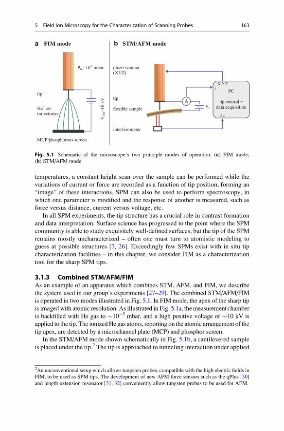
3.2.4 Radius Determination by Ring CountingThe most straightforward way to determine the radius of an FIM tip is to use the
“ring counting” method [12, 37, 46]. With the assumption that the apex of the tip
has spherical envelope, one can count the number of atomic steps between crystal-
lographic planes, which show up as “rings” in the FIM micrograph, and determine
the radius by simple geometry (to follow). A spherical envelope is a good approx-
imation within the region of the tip in which we are interested – ball models of tips
created by cutting a bcc crystal in a hemisphere give good correspondence to the
features seen in FIM images. It is worth noting that more elaborate techniques have
5 Field Ion Microscopy for the Characterization of Scanning Probes 169
been developed to extract the surface profile of FIM tips from features in micro-
graphs [47, 48], essentially by using ring counting between various crystallographic
poles to extract Cartesian (x, y, z) coordinates of the surface atoms. These are
particularly useful if one is interested in determining the cross-sectional profile out
into the far edges of the FIM image (which in our case is blocked by an aperture).
The ring counting method can be described as follows [12]: Assuming a spherical
envelope of the tip apex, the local radius of curvature, R, between two crystallo-
graphic poles separated by angle y can be found by counting the number of visible
rings, n, between them. Using the interlayer spacing, s, corresponding to the appro-
priate crystal plane, the local radius of curvature is given by
R ¼ ns hklð Þ1� cos y
: (5:5)
This equation describes the geometry illustrated in Fig. 5.5.
For the ring counting estimations to be accurate, each counted ring
must correspond to a single atomic step of type (hkl). We will soon demonstrate
that in FIM micrographs, a single “ring” can correspond to multiple atomic
planes of height s – counting rings is not equivalent to counting steps. The
underestimation of FIM tip radii can occur when the rings appearing in the
micrograph correspond to more than one atomic plane. The standard description
of ring counting could be more precisely expressed in the following way: assuming
a spherical envelope of the tip apex, the local radius of curvature is determined by
counting the number of steps, n, of height s between crystallographic poles with
angle y between them.
The ring counting method can be applied to different choices of (hkl) pole, butthe rings of the (110) plane are the most straightforward to identify because they
have the largest step height in the bcc crystal. The (110) plane also happens to be the
apex of most polycrystalline tungsten tips as a consequence of the wire’s
manufacturing by cold drawing [44].
In Fig. 5.6, we present ball models of tungsten tip apices of radii 3.0, 4.7, 6.0, and
9.0 nm. The models were created by carving a hemispherical shell from a bcc crystal
with a (110) apex. The atoms in the outermost 0.05 nm shell are shaded lighter in
Fig. 5.5 FIM tip apex with
radius R showing geometry
for ring counting. Planes of
interlayer spacing s arenormal to direction (hkl), andn rings are counted between
poles (hkl) and (h0k0l0). Theangle between these poles is y
170 W. Paul and P. Gr€utter

order to highlight the atoms at terrace edges which would be imaged brightly in FIM
(a common method of visualizing atomic geometry with ball models [49, 50]).
As the tip radius increases, the size of crystallographic facets increases – for
example, the (211) facet has just two rows of atoms in Fig. 5.6a but has five rows of
atoms in Fig. 5.6c. Correspondingly, the number of rings increases between the
centers of crystallographic poles. From Eq. 5.1, we have calculated the expected
number of rings n between the (110) apex and the (111) and (211) poles, indicated
in Fig. 5.6 with corresponding white and black circles. The centers of these planes
are indicated by circles on the ball models.
The expected number of rings corresponds well with the number of rings
counted from the tip apex to the center of the crystallographic poles (the rings are
indicated by concentric quarter circle lines at the edge of the (110) steps). The
number of rings can be thought of as the number of (110) steps that must be
descended from the (110) apex in order to reach the center of the (h0k0l0) pole in
question. For these tips of relatively small radii and for the small angles between the
apex and the (111) and (211) directions, there is a single (110) plane for each ring;
therefore, the estimation of ring counting is accurate.
Comparing the calculated number of rings to the rings visible in the ball models,
it is apparent that a better estimation of the tip radius is obtained using a count of
n–1 instead of n: this off-by-one error can be explained in Fig. 5.5 where it is the
a b
c d
Fig. 5.6 Top view (looking
toward the apex) of ball
models of W(110) tips with
radii (a) 3.0 nm, (b) 4.7 nm,
(c) 6.0 nm, and (d) 9.0 nm.
Quarter-circle lines highlight
the (110) rings at step edges.
The center of the (111) and
(211) poles are indicated by
white and black circles,respectively
5 Field Ion Microscopy for the Characterization of Scanning Probes 171

number of steps crossed to get from (hkl) to (h0k0l0) that matters (one less than the
total number of rings). This is usually a small correction but becomes increasingly
important with decreasing tip radius. This concern is equivalently expressed by
starting to count rings at 0 rather than 1, as done by Webber [46].
The first serious error that can occur in ring counting consists of counting FIM
rings which correspond to more than one atomic plane of type (hkl). This becomes
problematic when rings are counted between planes of large angular separation
(e.g., (110) type planes that are 60� apart [51]). Shown in Fig. 5.7 is the side view of
the 6.0 nm tip presented in Fig. 5.6c. Counting the rings between (110) and 011� �
yields nine rings, indicated by red arrows on the right half of the image. As the angle
from the apex increases, the visible rings begin to correspond to more than one
(110) plane. This is illustrated by the blue “ruler” on the left half of the image where
we have counted 15 atomic planes between the (110) apex and the center of the
(101) plane. Using n = 9, we obtain a radius of 4.0 nm, whereas a more accurate
estimate is obtained using n–1 = 14, yielding a radius of 6.2 nm.
A second common ring counting error arises from the use of the wrong interlayer
spacing. The interlayer spacing s must correspond to that of the (hkl) pole – the
initial pole – not (h0k0l0), the final pole. Using the (111) plane spacing rather than
(110), Urban et al. [52] deduced a tip radius of 14.4 nm, whereas we estimate a
radius of the order �32 nm by counting �21 rings from (110) to (211). These
problems are again seen in Pitters et al. [53] where the 3 and 5 nm radii tips
determined by the authors are actually of the order 6 and 10 nm, and also in
Rezeq et al. [54] where the 1.4 nm radius apex should be �4.8 nm (although the
image resolution makes the identification of (110) and (111) planes difficult).
To summarize, the key elements to proper radius determination by ring counting
are as follows:
Fig. 5.7 Side view of the 6.0 nm radius W(110) tip presented in Fig. 5.6c. There are 15 layers of
(110) planes between the apex and the (101) facet (dark blue lines), but only 9 “rings” apparent inthe micrograph (red arrows). The estimation based on 14 � 0.446 nm yields a radius of 6.2 nm,
whereas 9� 0.446 nm yields an underestimated radius of 4.0 nm. The (111) apex is shown at layer
#6 from the (110) apex. The angle between (110) and (111) is sufficiently small that the number of
rings corresponds exactly to the number of (110) steps
172 W. Paul and P. Gr€utter

• n must be accurately determined – its value must correspond to the number
single steps of type s.• s must correspond the plane spacing of (hkl), not (h0k0l0).• n should be replaced by n–1 for a more accurate radius estimation for small tips
(or equivalently, counting should begin at zero)
We also urge the use of (110) planes for ring counting due to their large step
height and not (111): rings corresponding to single (111) steps are very difficult to
discern because of the small (111) step height. The routine construction of ball
models of FIM tips also helps to familiarize the experimenter with the appearance
of tips with different radii.
Finally, to quickly estimate a tungsten tip radius in nm, one can simply multiply
the number of rings from (110) to (211) by 1.66 nm · ring�1 or multiply the number
of rings from (110) to (111) by 1.21 nm · ring�1 (these factors are s(110)/(1–cosy)).
3.2.5 Advanced Tip Preparation: Etching and FacetingIn this section, we mention other tip preparation techniques beyond the standard
procedure of tungsten tip etching and FIM characterization. Gas etching and tip
faceting are well established in the FIM community and offer exciting opportunities
to atomically engineer the apices of SPM tips.
The sharpening of tips using nitrogen gas is rather straightforward and has been
well studied in the context of building sharp tips for field ion emission in helium ion
microscopes or electron emission for coherent electron sources and point projection
microscopes. The nitrogen sharpening process was first reported by Rezeq
et al. [54] and patented by the same authors in 2008 [55].
The process occurs by adsorption of nitrogen on the tungsten tip shank, illus-
trated in Fig. 5.8. The nitrogen cannot bind to the very apex of the tip because the
electric field there is too large – the gas is ionized and repelled before it can reach
the tip surface. Nitrogen can, however, bind to the shank of the tip where the field is
not as high. This happens by dissociative adsorption in which a single nitrogen atom
forms a chemical bond to a tungsten atom on the tip’s surface (this reaction is
discussed in Sect. 3.2.6 and is addressed specifically in Refs. [56, 57]). The W-N
bond weakens the W atom’s bond to its neighbors and lowers the field necessary to
evaporate the W-N complex, shown schematically in the patent illustration
reproduced in Fig. 5.8a, b.
The weakened tungsten atoms are thus preferentially etched by field evaporation
from the tip shank. The resulting reduction in the local radius of curvature of the tip
apex is illustrated in Fig. 5.8c. The final profile of the tip is somewhat different than the
original: a shoulder is formedwhere the field on the shank is no longer strong enough to
evaporate theW-N (this shape has been experimentally verified by SEM in Ref. [52]).
At its apex, the radius is much reduced and can be etched to terminate in a single atom.
One distinct advantage of this tip sharpening technique is that it can be monitored
by helium ion FIM imaging during the etching process. Figure 5.9a–e shows a
sequence of FIM images during nitrogen sharpening of a W(111) tip at room
temperature, beginning at a radius of �4.3 nm and ending with a radius of �2.5 nm
5 Field Ion Microscopy for the Characterization of Scanning Probes 173
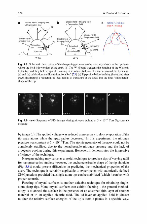
by image (d). The applied voltage was reduced as necessary to slow evaporation of the
tip apex atoms while the apex radius decreased. In this experiment, the nitrogen
pressure was constant at 5� 10�7 Torr. The atomic geometry of the apex could not be
completely stabilized due to the nonadjustable nitrogen pressure and the lack of
cryogenic cooling during this experiment. However, it demonstrates the impressive
efficiency of the technique.
Nitrogen etching may serve as a useful technique to produce tips of varying radii
for nanomechanics studies; however, the uncharacterizable shape of the tip shoulder
(Fig. 5.8c) could present difficulties in predicting the mechanical properties of the
apex. The technique is certainly applicable to experiments with atomically defined
SPM junctions provided that single-atom tips can be stabilized (which it can be, with
proper control).
Faceting of crystal surfaces is another valuable technique for obtaining single-
atom sharp tips. Many crystal surfaces can exhibit faceting – the general method-
ology is to anneal the surface in the presence of an adsorbed thin layer of another
material or in an applied electric field. The ad-layer or applied field is chosen
to alter the relative surface energies of the tip’s atomic planes in a specific way.
a b cElectric field = Imaging field< Evaporation field
Electric field = Imaging field< Evaporation field
Electric field ≥Evaporation field
Electric field <Imaging field
Electric field <Imaging field
Adsorbed and
dissociated N
protruding
W atoms
Adsorptionsite
W atoms
W Tip
N2
N2
+++
W Tip
+++2
1
10
4
3
Fig. 5.8 Schematic description of the sharpening process. (a) N2 can only adsorb to the tip shank
where the field is lower than at the apex. (b) The W-N bond weakens the bonding of the W atoms
to the tip, and they field evaporate, leading to a preferential loss of material around the tip shank.
(a) and (b) public domain illustration from Ref. [55]. (c) Tip profile before etching (blue), and after(red), illustrating a reduction in local radius of curvature at the apex and the final “shouldered”
shape of the tip
Fig. 5.9 (a–e) Sequence of FIM images during nitrogen etching at 5 � 10�7 Torr N2, constant
pressure
174 W. Paul and P. Gr€utter

Then, annealing the tip under such conditions allows the low energy planes to
expand and intersect, forming an atomically-sharp nano-pyramid at the tip apex.
Much of the initial surface science investigation of faceting systems such as the
W(111) surface under adsorbed Pd (as well as other noble metals), W(111) under
oxygen, and Ir(210) under oxygen was conducted by Ted Madey’s group under
LEED and STM investigation of the surfaces of bulk crystals [58–60]. Tien
T. Tsong, who worked on FIM from its inception, has succeeded in transferring
many of Madey’s surface science systems to the apices of sharp FIM tips in order to
engineer faceted single-atom tips [61–68]. All of these studies (with exception of
the Ir(210) tips) involve the expansion of the (211) planes on a W(111) tip until its
apex becomes a three-sided pyramid formed by the intersecting (211) planes (for
reference, a W(111) tip can be seen in Fig. 5.4d). The faceting of the Ir(210) surface
under oxygen exposure forms a pyramid from the (311), 311� �
, and (110) planes
with a single-atom apex pointed in the (210) direction [64].
Tip faceting by thermofield annealing (annealing under a large electric field)
favors the growth of large (110) terraces. Applied to a W(111) tip, it can be used to
create a pyramid in the opposite manner as described for noble metal plating – the
(110) terraces expand until they intersect to form a three-sided pyramid at the expense
of the (211) planes [69–72]. Thermofield annealing has the advantage of being
carried out without the need for an adlayer of oxygen or metal on the tip surface.
The pyramidal geometry of faceted tips would be of considerable interest not
only for atomically defined SPM experiments but also in atomic-scale
nanoindentation experiments due to the simple relationship between their projected
contact area and penetration depth (a desirable feature which is exploited in
traditional nanoindentation testing [73]).
3.2.6 Tip Integrity: “Force Field” Protocol and Rest GasesIn order to carry out an SPM experiment with an atomically defined FIM tip, it is
necessary to address issues of tip integrity. This is to ensure that when used in SPM,
the apex is identical to that characterized in FIM. We will first discuss what is
known about the reaction of gas molecules with the surface atoms of tungsten tips
and then present a protocol to ensure that the tip structure remains intact between
FIM and SPM. Another matter to be considered is how long the atomic structure of
the tip is expected to last due to the finite rest gas pressure in UHV – this will
determine how promptly an experiment must be performed such that the atomic
configuration of the apex is known with reasonable statistical confidence.
The interaction of gases with metal surfaces was studied extensively in FIM by
Erwin M€uller (the inventor of FIM) at Penn State University, Gert Ehrlich at the
University of Illinois at Urbana-Champaign, and Holscher and Sachtler at Shell
Research in the Netherlands in the early 1960s. Here, we review the experimental
findings for the adsorption of typical rest gases found in a UHV system (N2, CO, O2,
H2O, and H2) on tungsten tips.
Nitrogen adsorbs on tungsten by dissociation, that is, as a single N atom chem-
ically bound to a W tip atom [57]. When imaged, it appears brighter and larger than
regular tip atoms [74]. However, the N-W bond is very strong and weakens the W’s
5 Field Ion Microscopy for the Characterization of Scanning Probes 175

bond to its neighbors. Due to the weakened substrate bonding, the N-W complex
may field evaporate (as a unit [16]) at fields lower than those necessary for imaging
[56]. Missing W atoms in an FIM image could therefore be an indication of
N adsorption.
Carbon monoxide is less corrosive than N2 [57]; however, it was still found
to remove substrate atoms when field desorbed, leaving behind vacancies [75].
Oxygen corrodes tungsten in a manner similar to nitrogen, though less aggressively
[57]. Again, the presence of oxygen is inferred by missing atoms [76]. Water was
shown to remove tungsten atoms down to liquid He temperatures [57].
The adsorption of hydrogen has no corrosive effect on tungsten tips, nor can it be
detected in FIM imaging [57, 77]. However, changes in field emission are detect-
able upon hydrogen adsorption.
In summary, the bonding of gas molecules to tungsten tips often occurs by
dissociation of the molecule and a weakening of the bonding of the underlying
W atom to its neighbors. The weakened backbonding leads to the phenomenon of
adsorbate-induced field desorption during imaging. Therefore, both bright spots and
missingW atoms in an FIM image are evidence of gas adsorption. For the interested
reader, Table 5.1 recounts in more detail the results of adsorption studies of several
types of gases on both tungsten and iridium tips.
Dedicated FIM systems have very stringent vacuum requirements due to their
intended application to adatom diffusion. They are designed for high-temperature
bakeout (limited to 300 �C by the microchannel plate (MCP)), and extreme pro-
cedures are carried out in order to minimize gas evolution [79].4 In less ideal
systems where the FIM is combined with other instrumentation (i.e., an SPM),
one will likely have a larger concentration of corrosive gas molecules in the system
during FIM imaging than under normal UHV conditions [80].5
Figure 5.10 demonstrates the rapid modification of an FIM tip by imaging gas
impurities. Starting with the clean tip apex prepared by field evaporation
(Fig. 5.10a), we momentarily lower the imaging voltage from 5.1 kV to 0 V and
back (this procedure took 40 s). The image in Fig. 5.10b shows the changes that
have occurred to the tip’s atomic structure in this short time. This image is a color
superposition image6 in which the initial image appears in green and the subse-
quent image appears in red. Atoms which have been removed from the initial
image are colored green, and those that have appeared in the second image are
colored red. Both red and green sites are evidence of gas adsorption, and the �30
changes visible on the tip’s 120 nm2 surface area are certainly not encouraging to
4For example, the MCP is bombarded by 200 eV electrons for many days to remove gas atoms
trapped in the channels.5Even in the case of admitting ultrapure He through a heated quartz tube, the normal pumping
speed of the UHV system may have to be sacrificed during FIM. In our case, the turbo pump must
be valved off as the heated quartz cannot provide a sufficient flux of He to reach 10�5 mbar.6A technique used by M€uller with film and color photographic printing to identify individual
changes among the many atomic sites on a FIM tip [81]. Here, it is done digitally.
176 W. Paul and P. Gr€utter

the prospect of maintaining the atomic-scale tip structure long enough to do an
SPM experiment with it!
Thankfully, all is not lost: due to the much higher ionization energy of He
compared to all other gases [82], when large fields are applied to the tip (in the
vicinity of the FIM imaging voltage), impinging gas molecules are easily ionized
and will be repelled from the tip before they can chemically react with the tungsten
atoms on its apex. We have found experimentally that reducing the tip voltage to
�80 % of the FIM imaging voltage is sufficient to prevent contaminant gases from
reacting with tip atoms over extended periods of time. We call this the “force field”
method and demonstrate its efficacy in Fig. 5.10b and c where no changes to the
atomic structure of the tip can be identified.
Table 5.1 Adsorption and corrosion behavior of various gases on tungsten and iridium FIM tips
Gas Tungsten tips Iridium tips
N2 Adatoms appear bright, larger. Adatoms
observed on highly corrugated planes and at
steps – not within the close packed (110), but at
the edges. More adatoms near (310) rather than
(111) – this anisotropy is attributed to
difference in N2 dissociation rate [74]
N2 adsorbs as a molecule (without
dissociation) between Ir atoms.
Much less corrosive to Ir than it is
to W (weaker bond) [57]
Nitrogen binds strongly to W. Perturbed by the
act of adsorption, the W can be field evaporated
at regular imaging fields [56]
N binds on top of W sites (the N2 molecule is
dissociated, measured by mass spectrometry).
Most N field desorbs before the ion emission is
bright enough to be photographed (missing
atoms could be sites of previously adsorbed N).
W atoms were removed at fields lower than
useful for imaging [57]
W-N complexes field desorb as a unit, reported
in the first paper on the time-of-flight atom
probe [16]
CO Found to be less corrosive than N2. During
FIM, CO is most corrosive when dissociated
due to O adsorption on W which removes
W substrate atoms. CO is dissociated by the
energetic electrons removed from the He+
during the FIM process. Adding H2, as a source
of even higher energy electrons (in addition to
the He imaging gas) enhanced the dissociation
rate of CO [57]
Much less corroded than W [57]
CO adsorption was found to rearrange substrate
atoms. At 300 K, this leads to surface corrosion
leading to vacancies underneath adsorbed
molecules. Chemisorbed CO leads to
“promoted field desorption” whereby the
adsorbed species evaporates before it can be
imaged, leaving behind a vacancy [75]
(continued)
5 Field Ion Microscopy for the Characterization of Scanning Probes 177

The following “force field” protocol is therefore suggested to preserve the tip
apex from gas impurities in FIM/SPM experiments:
1. Prepare a clean tip by field evaporation in FIM.
2. Reduce applied voltage to �80 % (“force field”).
3. Pump imaging gas, refill liquid nitrogen cold traps, flash TSP while “force field”
is on.
4. Ramp down “force field” voltage when base pressure has recovered.
5. SPM experiment.
Finally, we must consider the fact that during the interval of the SPM experi-
ment, the FIM tip will be subjected to contaminants in the UHV rest gas. We will
consider the likelihood of rest gas molecules impinging on a 1.16 nm2 area which
corresponds to the area of the W(111) tip trimmer apex, plus the perimeter of the
second layer of atoms on which it is supported [80]. The following estimations
establish an upper bound on tip contamination as adsorption probabilities are
considered to be unity.
The gas composition of the UHV rest gas was measured by a residual
gas analyzer (RGA) (located in a different – but similarly pumped – UHV chamber
used for sample preparation) yielding pressure fractions of the individual
rest gas species, ni. Using the total pressure reading of our measurement
Table 5.1 (continued)
Gas Tungsten tips Iridium tips
O2 Seems to be less corrosive than N2, but not as
extensively studied [57]
W-O complexes are field desorbed together,
observed in Ar ion FIM [78]
W-O complexes field desorb as a unit, reported
in the first paper on the time-of-flight atom
probe [16]
In He ion FIM, adsorbed oxygen cannot be
directly observed on the surface; its presence is
inferred from corrosion damage [76]
H2O Studied in J. F. Mulson PhD thesis. Shown to
remove W surface atoms (as well as Pt), even
when surface is kept at liquid He temperature
[57]
H2 Adsorption causes significant changes to the
field emission pattern of the tip. However, no
change can be detected in FIM. During FIM, a
perturbation of the adsorbed H2 layer is
attributed to the bombardment of electrons
coming from ionized He+ imaging gas [77]
H2 could not be imaged, but removal
of atoms, particularly in the bright
(110) zone boundary, is attributed to
H2 adsorption [57]
H2 did not have a corrosive effect and could
also not be detected [57]
178 W. Paul and P. Gr€utter

chamber gauge, Pgauge = 5 � 10�11 mbar, the partial pressures, pi, of the compo-
nent gases can be calculated from
pi ¼ niPgaugeXi
Ki
KN2
ni
; (5:6)
whereKi=KN2is the ionization sensitivity of individual gas species relative to that of
N2 [83]. Combining the Maxwell-Boltzmann velocity distribution of the gas parti-
cles with the ideal gas law [84], we obtain the flux of each species as
Fi ¼ piffiffiffiffiffiffiffiffiffiffiffiffiffiffiffiffiffiffi2pmikBT
p ; (5:7)
where mi is the atomic mass of the gas species, kB is the Boltzmann constant, and
T is the temperature.
a
b
Imaging voltage lowered to 0V
momentarily (40s)
Imaging voltage lowered to 80%
for 10 min
70 minutes with nofield applied after
pumping imaging gas
c
d
e
f
Fig. 5.10 (a) (110) tip at 5.1 kV; (b) color superposition image of (a) with the FIM image after
the imaging voltage was momentarily lowered and raised – about 30 atomic sites show modifica-
tions; (c) (110) tip at 5.0 kV; (d) color superposition image of (c) with the FIM image after waiting
10 min with the voltage lowered to 4.0 kV – no changes are observed to the atomic structure; (e)(111) tip at 6.0 kV; (f) color superposition image of (e) with the FIM image after waiting 70 min in
UHV (From Ref. [80] # IOP Publishing. Reproduced with permission. All rights reserved)
5 Field Ion Microscopy for the Characterization of Scanning Probes 179

The probability of k gas molecules arriving in area A on the tip during time t isgiven by a Poisson distribution (assumes arrival is independent of time and loca-
tion) [85]:
P kð Þ ¼ e�FAt FAtð Þkk!
: (5:8)
The probability of obtaining more than one arrival on the tip apex area (i.e., k > 1)
can be easily obtained using the property that the distribution is normalized:
P k > 1ð Þ ¼X1k¼1
Pk ¼ 1� P0 ¼ 1� e�FAt: (5:9)
The rate of tip contamination is described in two ways: In the first way, we
calculate the duration of an experiment such that in 5 % of experiments of this
duration, more than one gas molecule would have impinged on the apex (i.e., on
average, 1 in 20 experiments having this duration would be carried out with a
modified tip). In the second way, we calculate the probability of more than one gas
molecule impinging on the apex during a 60 min delay (chosen as a minimum
reasonable SPM experiment duration which must include tip transfer, sample
approach, etc.). The results of these calculations are shown in Table 5.2. Note
that other unidentified gases (not listed) make up 2.2 % of the gas composition,
meaning they have approximately the same statistics as N2.
We notice immediately that hydrogen is problematic because of its high pressure
fraction and flux (the latter due to its low mass). However, its presence goes
undetected in the methods employed here – FIM characterization is blind to hydro-
gen, and it is known to have no corrosive behavior to tungsten tips [57]. After
hydrogen, the next most common gases (H2O, N2, and CO) are at a nearly acceptable
background level if an experiment is completed within a short period of time (�1 h).
Figure 5.10e illustrates the typical rest gas contamination of our tungsten tips
which have been preserved with a “force field” until the UHV system had returned to
base pressure. The tip was left in UHV for 70 min after the “force field” was turned
off. The color superposition image in Fig. 5.10f shows changes to �30 atomic sites.
(The number of changes is overestimated due to contamination during the FIM start-
up procedure [80].) Assuming an approximate mass of 28 amu, the changes to the tip
during this time interval indicate an effective contaminant pressure of �2 �10�11 mbar. This number is consistent with the calculations presented in Table 5.2
and the expected overestimation of contamination due to the FIM start-up procedure.
Experiments with atomically defined tips must be performed quickly, even in a
clean UHV environment. This has important consequences for the design of a
combined FIM/SPM experiment: since the sample should also not be subjected to
contamination from the imaging gas, the tip (or sample) must be transferred from a
separate vacuum chamber in a reasonable time frame, and the coarse approach of
the tip to the sample surface must be done with minimal delay.
180 W. Paul and P. Gr€utter

Table
5.2
TableoftypicalUHVrestgas
species,theirpartialpressures,fluxes,andcalculatedcontaminationtimes
andprobabilitiesfora1.16nm
2tipapex.
H2O
islikelyoverestimated
dueto
theRGA
locationin
thesample
preparationcham
ber
whichisnotas
thoroughly
baked
andissubjected
totheregular
introductionofnew
samples(From
Ref.[86].#
IOPPublishing.Reproducedwithpermission.Allrightsreserved)
Species
Mass,
m(amu)
Ionization
sensitivity,
Ki=K
N2
Pressure
fraction,n i
Partialpressure,
pi(m
bar)
Flux,
F(nm
�2s�
1)
1:20apex
contaminationtime
(min)
P(k
>1)gas
atom
onapex
duringa60min
delay
H2
20.42
88.0
%9.4E-11
1.0E-03
0.7
98.5
%
H20
18
0.9
4.6
%4.9E-12
1.8E-05
41
7.1
%
N2
28
12.3
%2.4E-12
7.0E-06
100
2.9
%
CO
28
1.2
1.7
%1.8E-12
5.2E-06
140
2.1
%
CO2
44
1.4
1.1
%1.2E-12
2.7E-06
270
1.1
%
He
40.16
0.1
%1.1E-13
8.1E-07
890
0.3
%
5 Field Ion Microscopy for the Characterization of Scanning Probes 181

3.3 Key Research Findings
3.3.1 Review of Combined FIM/SPM ExperimentsA handful of groups pioneered the combination of FIM and SPM from the
mid-1980s to the late 1990s. Here, we review the work of the principal groups in
this field in an approximately chronological order.
The first report of combined FIM and STM techniques was from Kuk and
Silverman working at AT&T Bell Laboratories in New Jersey. Their investigation
focused on the observed corrugation height (constant current STM topography) of
the rows of the (1 � 5) reconstructed Au(100) surface using a W(100) tip at room
temperature [87]. The same results also appear in a well-cited paper about STM
instrumentation published in 1989 [88]. We are not aware of any further publica-
tions containing FIM results from these authors.
Toshio Sakurai’s group from Tohoku University in Sendai, Japan, published
quite extensively about combined FIM and STM in a technique they refer to as field
ion-scanning tunneling microscopy (FI-STM). By 1989, Sakurai had built a series
of room-temperature FI-STMs [89]. A review article on the FI-STM technique
appeared in Progress in Surface Science in 1990 [90]. In the early 1990s, the group
focused on silicon surfaces and worked to study the surface bonding of C60
molecules [91–93] and alkali metals [94]. In these studies, the FIM was used to
confirm tip cleanliness and sharpness in order to help obtain reliable atomic
resolution in STM. The role of the tip’s atomic structure in STM imaging was not
an explicit concern in this work. The group of Yukio Hasegawa, who worked with
Sakurai, later demonstrated FIM characterization of a tip mounted to a length
extension resonator for AFM [95].
Some very diligent combined FIM/STM work was carried out by Masahiko
Tomitori et al. while based at the Tokyo Institute of Technology, Yokohama, Japan,
between �1990 and 1996. The first work investigating STM tip approach was
performed in air on freshly cleaved highly oriented pyrolytic graphite (HOPG), and
the Pt-Ir alloy tips were transferred to and from vacuum for FIM characterization
[96]. The goal was not to implement atomically defined tips in air; they wanted to
ensure that the tip apex did not crash into the substrate inadvertently during coarse
approach. Tomitori underlined the necessity in performing the tip approach within the
bandwidths of the STM feedback loop and current preamplifier – exceeding these
bandwidths could result in crashing the tip without any sign of a current spike arising
frommechanical contact. Approaching the tips too quickly was found to render the tip
apex nonobservable in FIM; a large amount of carbon, hydrogen, and oxygen had also
been transferred to the tip apex, detected by a time-of-flight (ToF) mass spectrometer.
In 1996, Tomitori published scanning tunneling spectroscopy (STS) results with a
“buildup” pyramidal tip in UHV [97]. The motivation here was to try to develop an
experimental procedure to obtain reproducible STS data by controlling the tip
geometry – that way, the STS technique could be more straightforwardly applied to
unknown samples. STS was carried out on the Si(111)-7� 7 surface in 64� 64 point
arrays in order to average over the surface unit cell, and spectra were found to
be reasonably repeatable with the tips as long as the bias range was kept within
182 W. Paul and P. Gr€utter
�2 to +2 V. Tips retained similar patterns in field emission microscopy (FEM)7 with
slightly modified voltage thresholds for imaging (perhaps indicating slight tip
changes). Expanding the STS bias range to �3 to +3 V altered the STS spectra
radically, and FEM showed large changes present on the tip, attributed to the
transferral of Si atoms from the substrate.
These two studies by Tomitori provided valuable early insights into the imple-
mentation of atomically defined tips in STM: feedback and current detection
bandwidths must be respected to avoid tip crashing on approach, FEM might be a
less awkward way than FIM to check for tip changes due to the absence of potentially
corrosive imaging gas, and STS can be implemented without significant tip changes
as long as the bias voltages are kept within a small enough range (�2 V).
At the University of Arizona, a combined STM with a ToF atom probe was built
by Uwe Weierstall and John Spence in the mid-1990s. They called the instrument
the scanning tunneling atom probe (STAP), and it was intended to be a means of
supplementing the STM with chemical identification in a kind of “atomic tweezer.”
The goal of this instrument was to transfer a chemically unknown species from the
sample to the tip, say by pulsing the STM bias voltage, and then switch over to ToF
mode to identify the chemical species ejected from the tip. Their first report in 1996
demonstrated the proof of concept of the STAP [98]. The atom probe’s mass-to-
charge detection was calibrated by W3+ and W4+ field evaporated from tungsten
tips, and the authors presented a preliminary result measuring a handful of Si atoms
transferred from an Si(111)-7 � 7 surface to a tip apex, as identified both in STM
imaging and ToF mass spectrometry.
A second and final paper from this instrument was published in Surface Science
in 1998 [99]. Although FIM-characterized tip apices were not an objective of their
work, some aspects of this second paper are relevant to the implementation of
atomically defined tips in current endeavors. ToF revealed that some care had to be
taken in order to not overshoot the tunneling current set point upon initial approach
and transfer Si atoms from mechanical contact (also noted by Tomitori). The
authors report statistics on an impressive number of experiments: after improving
their tip approach procedure, in �80 % of about 50 experiments, W tips could be
scanned and returned for ToF analysis without having picked up Si atoms. In
�20 % of cases, a tip change occurred while scanning, often accompanied by a
sudden improvement in STM resolution, and this correlated with the ToF detection
of Si transferred to the probe tip.
Although single-ion sensitivity is possible with their chevron microchannel
plate, the open area of the detection channels is only �60 %. Nevertheless, the
statistics are quite convincing that W tips can be approached to tunneling proximity
in STM without the transferral of atoms from the substrate, but tip changes seen
during STM scanning correlate with atom transfer. FIM imaging of the tip was not a
7FEM operates in a similar manner to FIM, but a field emission current is detected rather than field
ionized gas atoms. A spatial map of the field emission current is visualized on an MCP/phosphor
screen when the tip is negatively biased. The technique does not allow the atomic structure of the
tip to be imaged.
5 Field Ion Microscopy for the Characterization of Scanning Probes 183

goal of this work, but the studies are valuable from the standpoint of considerations
of material transfer which would modify atomically defined FIM tip apices when
they are used in STM.
Manfred Leisch’s group at the Graz Institute of Technology, Graz, Austria, built
a position-sensitive atom probe detector to be used in conjunction with a commer-
cial Omicron STM-1. The goal of this system was to investigate the mechanical
interaction between materials on the atomic scale [100]. This was essentially an
experimental realization of the systems studied in early molecular dynamics
simulations to address atomic-scale contact formation, wetting, adhesive bonding,
connective neck formation, and plastic deformation [101]. The experimental
investigation of mechanical interactions between tips defined in FIM and other
specimens was not particularly new – this had been investigated to some extent in
the 1960s and 1970s by M€uller and Nishikawa [102], but the lack of control over
interaction forces between the tip and contacting specimen made it difficult to
avoid destroying the delicate FIM tip. Leisch’s group identified that the
techniques developed for SPM (e.g., piezoelectric transducers, force, and current
feedback methods) were ideal for controlling mechanical interactions with FIM tips
at atomic length scales. Using STM control of the tip and a time-of-flight mass
spectrometer incorporated into the FIM, the number of atoms transferred from the
substrate to the tip during indentation could be counted. The authors also made
interesting observations about changes to the tip structure induced by STM
imaging [103].
3.3.2 Atomically Defined Tips in STMIn Sect. 3.2.6, we introduced the “force field” protocol to ensure that tip apices
remain unchanged between FIM and SPM, and we have also determined that they
can be kept atomically clean for a reasonable length of time for use in the SPM
experiment. Now, we report experimental results on bringing tips into tunneling
proximity with SPM samples.
Tomitori identified the necessity to keep the tip approach speed within the
detection bandwidth to avoid set point overshoot (which would result in tip
crashing; Sect. 3.3.1) [96]. In the case of STMwhere the tunneling current increases
at a rate of about one decade per angstrom, dangerous overshoot can be avoided by
limiting the approach speed to a maximum of�1,000 A/s. This is to allow sufficient
time for the distance regulation feedback loop to respond to regulate the tip distance
(a standard tunneling current amplifier has a bandwidth of a couple kHz, and typical
SPM feedback loops are tuned to respond in about �1 ms). We approach tips at a
speed of 200 A/s, resulting in negligible overshoot.
It turns out that the choice of substrate is very important in maintaining tip
integrity. We have investigated tip integrity after approaching FIM tips to several
types of STM samples: after reaching the tunneling set point and maintaining this
distance for a few minutes, tips were retracted and imaged again in FIM [80]. With
confidence that relatively few tip changes occur under this time delay due to the rest
gas (Sect. 3.2.6), we can study the effect of the interaction with the sample on the tip
structure.
184 W. Paul and P. Gr€utter

We summarize the approach of W(111) FIM tips to Au(111) and cleaved Si(111)
surfaces in Fig. 5.11. In both cases, the tip is approached to a tunnel current set point
of 6 pA. In the case of the Au(111) surface (Fig. 5.11a), the measured current is very
unstable – many spikes are apparent up to �40 pA throughout the experiment. The
tip is imaged again in FIM and reveals changes to the atomic structure in approx-
imately the entire field of view. Note that the underlying threefold symmetry is still
visible which indicates that the tip did not suffer mechanical damage during the
experiment (the large flat W(110) planes are mostly intact).
The observation of spikes and correlated FIM tip changes for Au(111) is
consistent with many other experiments on Au(111), as well as cleaved HOPG,
sputter-annealed InSb(001), and cleaved GaAs(001) [29].8 The presence of changes
to the tip apex must be due to interaction with the sample – the “force field”
protocol is very successful – but do the atoms which change the tip structure
come from the sample itself? Or could they be gas atoms physisorbed on the tip
tip after(modified by gold)
tip before unstable current measured betweentip and gold surface
tip after(unchanged)
tip before stable current measured betweentip and silicon surface
a Au(111) 6 pA, -0.08 V, T=298 K
b Si(111) 6 pA, +2 V, T=298 K
Fig. 5.11 FIM images before and after tunneling experiments with (a) Au(111) and (b) cleavedSi(111) at room temperature. Tunneling current snapshot shows the initial moment of approach of
the tip to the sample surface
8Though the frequency of spikes was very much less on some of these substrates, their presence
was still correlated with changes to the FIM tip.
5 Field Ion Microscopy for the Characterization of Scanning Probes 185

shank that migrate to the apex under the electric field gradient in STM? In order to
understand where the changes come from, we turned to cleaved Si(111), the most
reactive surface that could be easily prepared on our system [86].
Figure 5.11b shows that the tunneling current is exquisitely stable between FIM
tip and Si(111) surface. It also confirms that very little overshoot occurs when the
sample surface is first detected at 0.1 s. The tip apex is unchanged in the image
taken after the experiment. The strong correlation between spikes in the tunneling
current and tip changes visible in FIM suggests that material is transferred from the
sample surface to the tip. The changes to the tip are not due to gas molecules from
the shank – if this were the case, the experiments with a Si(111) surface would be
equally affected.
The temperature dependence of the tunnel current spikes and tip changes has
also been investigated for Au(111) by cooling the entire microscope (sample and
tip) to 158 K [104]. As Fig. 5.12 indicates, the magnitude of the current spikes is
much higher at low temperature (the vertical scale is the same in both Fig. 5.12a, b).
Interestingly, at low temperature, the modifications to the tip apex are confined to
the very center of the tip. The thermally activated diffusion of adatoms on the tip
is expected to be quenched at this temperature due to the large corrugation of the
W(111) surface [104]; therefore, the transferred atoms stay in place.
Though the result of localized tip modifications precludes Au(111) at 158 K as a
possible substrate for atomically defined tips in STM, it is a useful result for two
reasons: Firstly, it provides additional evidence that the changes to the tip, which
are localized to the very apex, originate from atoms transferred from the sample
rather than the tip shank.9 Secondly, it indicates that the expected W(111) crystal
plane is indeed the part of the tip which interacts with the sample (i.e., the
(111) direction is pointed along the tip wire axis, even after tip fabrication/etch-
ing/preparation procedures).
In order to carry out an experiment with an atomically defined tip, it is also
important to be able to identify events indicative of tip changes. In experiments on
cleaved Si(111), where the tunneling current is mostly stable, occasional tip
changes can take place while scanning. These tip changes are characterized by
simultaneous spikes in the tunneling current of order 50–100 pA (at 8 pA set point),
accompanied by changes in topographic scan height on the order of 10 pm (up to
130 pm), and often changes in the lateral resolution of the STM image [29]. We
expect that the �10 pm changes, which are very much smaller than interatomic
distances in crystals, may arise from a transferred atom which diffuses to a site
slightly off-center and weakly modifies the electronic density of states of the apex
atoms which are involved in tunneling.
Point defects on the cleaved Si(111) surface also provide an opportunity to study
tip changes because they image the tip itself in the form of an image convolution.
The tip structure is reflected in features repeated throughout the image.
9If the latter were the case, tip changes would be seen all over the apex region from chemically
bound atoms.
186 W. Paul and P. Gr€utter

For example, in Fig. 5.13a, b, a 2-lobed feature recurs in the constant current STM
image. We can draw a ball-and-stick model of this feature to scale (and in the
correct orientation) with the initial FIM image of the tip (Fig. 5.13e). This gives
some appreciation of where the STM imaging atoms (added by tip changes) might
be located with respect to the original tip geometry. The tip convolution features
change as STM scanning is continued, and another repeated motif is shown in
Fig. 5.13c, d for negative and positive biases, respectively.
As expected from the changing tip convolutions, the STM tip appears highly
modified when it is returned to FIM for imaging (Fig. 5.13f). It is imperative to
realize that the image displayed in (f) is just one image of many that are taken of the
tip structure which evolves during imaging due to field evaporation. FIM carried
out on a highly modified tip is a very unstable process for several reasons: the added
atoms protrude from the surface, so the electric field is locally enhanced at their
a Au(111) 6 pA, -0.08 V, T=298 K
be
fore
aft
er
time (s)
curr
ent (p
A)
curr
ent (p
A)
time (s)
b Au(111) 6 pA, -0.08 V, T=158 K
be
fore
aft
er
6.5 kV
7.3 kV
7.2 kV
7.2 kV
0 0.5 1 1.5 2
0
50
100
0 0.5 1 1.5 2
0
50
100
Fig. 5.12 FIM tip apices before and after, as well as a snapshot of the measured tunneling current
when approached to Au(111) at temperatures of (a) 298 K and (b) 158 K
5 Field Ion Microscopy for the Characterization of Scanning Probes 187

positions, leading to their facilitated field desorption.10 Because of their different
chemical nature, they will be subject to ionization and desorb at lower voltages than
tungsten would (the ionization field of almost every other atomic species is lower
than that of tungsten [12]). Because of the unstable atomic structure during FIM
imaging of a modified tip, it would be inappropriate to compare the image in
Fig. 5.13f to the features of the topographic STM images.
A concluding word of caution when inspecting FIM tips after STM experiments:
the tip is made from a crystal and is therefore self-similar. After field evaporating
three atomic layers from the apex, it will appear nearly indistinguishable from the
original tip.11 It is possible for the experimenter to be misled into thinking that the
2 nm10 nm
10 nm 10 nm
a b e FIM before
c d f FIM after
Fig. 5.13 (a) STM image showing a partially reconstructed Si(111) terrace. (15 pA, +2 V) (b)higher magnification image of a region shown in (a) highlighting the tip convolution feature.
(15 pA, +2 V) (c) Filled-state STM image of the same area after tip changes. (15 pA, �2 V) (d)Empty state STM image of the same area. (15 pA, +2 V) Lines running in the 10-o’clock to
4-o’clock direction correspond to the 2 � 1 surface reconstruction. (e) FIM image before STM
experiments with tip convolution model scaled to the appropriate size and direction. (6.4 kV) (f)FIM image after extensive STM experiments. (6.2 kV)
10The images of modified tips that we display are taken at as low a voltage as possible to minimize
tip changes, but it is impossible to determine how many atoms desorb before the onset of imaging.
Numerous images are acquired while the voltage is slowly increased; they are averaged together in
sets where the tip structure remains constant. The stability of modified tips may increase with
decreasing temperature. However, changing the temperature will not change the ionization field of
the adsorbed atoms relative to tungsten or the imaging gas.11It takes many layers of field evaporation to increase the radius significantly.
188 W. Paul and P. Gr€utter

post-STM tip is unchanged when he or she is in fact observing a new layer of atoms.
With the present availability of digital cameras and plentiful data storage, it should
be possible to acquire many frames and carefully assess the results.12 We urge
caution in the interpretation of early combined FIM/SPM studies which do not
discuss the fragility of tungsten tip apices due to their reactivity, the stability of the
tunneling current in STM, or the FIM imaging process after STM [87, 105].
At the time of writing, we are confident that STM imaging with pristine FIM tips
can be carried out, albeit for a very short period of time (�1 min to first tip change
on cleaved Si(111)). Tip changes are identified during STM scanning by disconti-
nuities in tip height, spikes in the tunneling current, and changes to STM resolution.
At room temperature, highly reactive sample surfaces are needed to reduce the
population of mobile adatoms on the surface which can transfer to and alter the tip.
Operating the experiment at a sufficiently low temperature to freeze out adatom
motion on the sample is another promising route to achieve atomically defined FIM
tips in SPM.
3.3.3 Long-Range Force Interactions in Noncontact AFMThe advent of new force sensors for noncontact AFM, namely, the qPlus [30] and
the length extension resonator [31, 32], has allowed tungsten FIM tips to be used in
noncontact AFM where until recently, microfabricated silicon cantilevers had been
most popular. FIM imaging of tip apices on length extension transducers has been
demonstrated by An et al. [95, 106], noting that field evaporation is a very effective
tip preparation technique for removing the surface oxides from tungsten. The
successful FIM characterization of a tip on a qPlus transducer was recently reported
by Falter et al. in 2013 [51]. This work constitutes a substantial advance in the use
of well-characterized tips because the authors use the FIM data in a quantitative
way to understand noncontact AFM results.
Falter et al. use the overall tip radius (from FIM) and cone angle (from supple-
mental SEM measurements) as input to models for electrostatic [107] and van der
Waals forces [108] acting between a spherically capped conical tip and a flat
surface. The authors were able to identify a strong variation of the contact potential
with distance at tip-sample separations less than 2 nm, indicating that the inhomo-
geneous work function of the faceted tip surface contributes localized patch charges
to the electrostatic force response. Detailed electrostatic models of SPM tips based
on FIM characterization may also help to elucidate atomic-scale contrast in the
contact potential measured by Kelvin probe force microscopy (KPFM) [109, 110].
3.3.4 FIM Tips for Atomic-Scale NanoindentationIn order to understand the mechanics of deformation during indentation, atomistic
simulations are often employed to provide a view “inside” materials while an
12In order to screen for tip changes during the STM experiment itself, one may want to acquire a
higher bandwidth version of the tunneling current signal throughout the entire experiment to
scrutinize carefully for spikes. By higher bandwidth, we mean the several kHz bandwidth of the
current preamplifier, rather than the �100 Hz pixel STM scan rate.
5 Field Ion Microscopy for the Characterization of Scanning Probes 189

indentation stress is applied [111]. These computer simulations are typically limited
to some millions of atoms and thus probe a much smaller volume than in traditional
nanoindentation. To close the length scale gap, the lateral size of indentation
experiments must be diminished by about three orders of magnitude. Nanometer-
sized indenters are also fundamentally interesting due to the breakdown of contin-
uum mechanics at this length scale – spherically shaped crystals contain stepped
facets which are expected to modify the contact pressure distribution when used for
indentation [112].
Preparation of tips by FIM is an ideal way to obtain a clean, atomically charac-
terized spherical apex with a radius of several nanometers. The strong covalent
bonding of tungsten gives the material stable performance under the high electric
fields of He ion FIM and makes it exceptionally hard [113]. High hardness is essential
to ensure that deformation occurs in the substrate rather than the indenter.
Using a combination of FIM, STM, and AFM (introduced in Fig. 5.1), we
have investigated the indentation response of Au(111) under indentation by
FIM-characterized tips [27, 29, 114–118]. We now discuss results of recent
experiments.
Referring to Fig 5.14, we now present typical features of an atomic-scale
nanoindentation curve in which a W(111) FIM tip is indented into a Au(111) single
crystal. The zero point of the indentation depth is set to the crossing of the 1 GOresistance of the conductance data (1 � 1 0�5 G0 in the example shown). This is a
1e–5
1e–4
1e–3
1e–2
1e–1
1e0
1e+1
1e+2
cond
ucta
nce
(G0)
–1 –0.5 0 0.5 1 1.5 2 2.5
–100
–50
0
50
100
150
200
250
300
depth (nm)
load
(nN
)
A
B
C
C
C
C
D
E
F
conductan
ce
out
out
G
in
inload
Fig. 5.14 A load-displacement curve showing important features in atomic-scale
nanoindentation response (see text). Load is blue and conductance is green upon loading the
contact (in-direction), load is black and conductance is red upon unloading the contact
(out-direction)
190 W. Paul and P. Gr€utter

semi-arbitrary zero point because zero separation is not well defined at these length
scales. A jump-to-contact is observed in the current (green) at point B where the
junction conductance suddenly increases to �3G0. At the points labeled C, abrupt
mechanical rearrangements occur in which the load decreases and depth increases
simultaneously (the slope of these changes corresponds to the stiffness of the force
transducer). These events are known as pop-ins and are attributed to the sudden
nucleation of plastic damage in the sample [119]. A pop-out is registered at point D,
interpreted as an event which partially reverses the plasticity created during load-
ing. The large adhesion force of the metallic contact is shown at point E. The
conductance upon unloading (red) shows a large hysteresis indicative of wire
drawing. This atomic-sized wire finally breaks at a conductance of just over 1 G0
at point F. G is an artifact from the long settling time of the current preamplifier and
should not be interpreted physically.
The adhesion of clean nanoscale contacts is remarkable in magnitude and is a key
factor differentiating response in these experiments from those of a traditional
nanoindenter. The two reasons for this are the exceptional cleanliness of the
indenter/surface system prepared in UHV and the large surface-to-volume ratio at
small length scales where energies required to create new surfaces are comparable to
those required to deform volumes [120]. Using FIM prepared tips, a strong depen-
dence of adhesion on the state of the tip has been observed [117]. After preparing an
atomically clean tungsten surface by field evaporation in FIM, the tip was repeatedly
indented into the pristine surface of a Au(111) single crystal. As indentation
progressed, the adhesive force dropped by a factor of 6� with a 1/e rate of 11–14
indentation cycles, indicating that the surface composition of the tip (in this
case, wetted by the gold substrate) strongly affects the measured mechanical
behavior. The FIM is therefore an ideal tool to create an experimental indentation
system with a well-defined surface composition for quantitative comparison with
atomistic simulations.
The determination of contact area and stresses during indentation depends on
accurate indenter characterization. With FIM-characterized W(111) indenters, the
minimum threshold for plasticity was investigated in Au(111) [116]. The indenter is
pictured in Fig. 5.15a, and stochastically initiated plasticity on the Au(111) single
crystal surface is shown in Fig. 5.15c before and d after indentation. The broad
distribution of yield-point shear stress suggested that dislocations were heteroge-
neously nucleated in this system. The resolution of very low forces and displacements
in AFM also permitted the extraction of energies required to produce defects in the
gold substrate: surprisingly, permanent impressions are left in the substrate by a
mechanical energy expenditure of only �70 eV.
The contact area during indentation, which can be inferred from the FIM tip
geometry, also yields important insights about electronic transport through the
indentation-formed nanocontact [115]. Experiments using a W(111) tip and
Au(111) sample yield a highly variable conductance in the range of
0.02–4.9 G0/nm2, which is much less than a Sharvin estimation of �13.8 G0/nm
2.
(The latter is expectedwhen each atom in themetallic contact contributes�1G0 to the
conductance.) The reason for the much reduced conductance between theW(111) and
5 Field Ion Microscopy for the Characterization of Scanning Probes 191

Au(111)metals was clarified by first-principles density functional theory calculations:
the d-wave electron modes of tungsten are poorly approximated by the s-wave modes
of gold, resulting in backscattering of electrons at the interface. Furthermore, disorder
and vacancies are also expected to diminish electron conduction. Electronic transport
across interfaces has obtained considerable attention in theoretical work [121–124],
but the experiments are rare due to the challenge in determining the contact area in
nanoscale systems [125, 126]. Because the geometry of FIM tips can be easily
modified by starting with wires of different crystal orientations and can be rotated
with respect to SPM substrates, one might expect them to find use in the study of the
electronic transparency of interfaces and disorder structures.
3.4 Conclusions and Future Perspective
Atomic-scale characterization of SPM tips by FIM provides a detailed view of the
tip structure which is usually unknown in SPM experiments. We have discussed the
operating principle and resolution of FIM, the preparation and radius determination
of the probes, and advanced tip preparation by techniques such as gas etching and
surface faceting.
In the implementation of FIM tips in SPM, we considered tip integrity with
regard to modifications due to chemical reaction with impurities in the imaging gas
and with UHV rest gases. We outlined the “force field” protocol which inhibits
a
c d
b
(112)
(110)
1 2 3 4 5
8 10
11 12 14 15
17 18 19
21 23 24 25
6 9
13
16 20
22
7
1nm
Fig. 5.15 (a) FIM image of the W(111) indenter (5.5 kV tip voltage); (b) ball model of a W(111)
with a 9.5 nm radius and Au(111) substrate to scale; (c) Au(111) terrace before and (d) after a 5� 5
indentation array with 20 nm spacing between indents (20 pA, �0.05 V sample bias). Boldednumbers indicate plastic sites, and italicized numbers indicate elastic sites (From Ref. [116]. Copy-
right 2013 by the American Physical Society)
192 W. Paul and P. Gr€utter

changes to the tips, guaranteeing the transferral of a pristine apex to the SPM
tip-sample junction.
At the moment, STM with a stable atomically defined tip has yet to be demon-
strated: at room temperature, tip changes occur within a short period of time on
many kinds of substrates. We expect that stable tips should be obtainable with the
construction of a stable cryogenic SPM with in situ FIM or with the use of very
reactive samples, such as Si(111)-7 � 7, at room temperature. Resolving the issues
of tip changes is an essential challenge to overcome in order to move the field into
more ambitious experiments such as the characterization of atomically defined
molecular junctions, quantitative understanding of local electrostatic forces from
faceted tips, and their use as benchmarking probes for materials with exotic
electronic properties (e.g., oxide electronics).
Their well-defined radii and chemical composition makes FIM tips ideal for
atomic-scale indentation. There are many open questions in this area which can be
experimentally addressed in detail, such as indentation by stepped indenters of
different geometries and surface chemistries. There is ample opportunity to borrow
techniques of advanced tip preparation (such as faceting) from the FIM community
and apply them to the study of nanomechanics, as well as the study of electronic
transport through mechanically formed nanocontacts.
References
1. Fink H-W (1986) Mono-atomic tips for scanning tunneling microscopy. IBM J Res Dev
30(5):460–465
2. Giessibl FJ, Hembacher S, Mannhart J (2004) Force microscopy with light-atom probes.
Science 305(5682):380–383
3. Campbellová A, Ondrácek M, Pou P, Perez R, Klapetek P, Jelınek P (2011) ‘Sub-atomic’
resolution of non-contact atomic force microscope images induced by a heterogeneous tip
structure: a density functional theory study. Nanotechnology 22(29):295710
4. Hofer WA, Redinger J (1998) Electronic structure of a realistic STM tip: the role of different
apex atoms. Philos Mag Part B 78(5):519–525
5. Kwapinski T, Jalochowski M (2010) Signature of tip electronic states on tunneling spectra.
Surf Sci 604(19–20):1752–1756
6. Sugimoto Y, Pou P, Abe M, Jelınek P, Perez R, Morita S, Custance O (2007) Chemical
identification of individual surface atoms by atomic force microscopy. Nature
446(7131):64–67
7. Ternes M, González C, Lutz CP, Hapala P, Giessibl FJ, Jelınek P, Heinrich AJ (2011) Inter-
play of conductance, force, and structural change in metallic point contacts. Phys Rev Lett
106(1):016802
8. Wagner RJ, Ma L, Tavazza F, Levine LE (2008) Dislocation nucleation during
nanoindentation of aluminum. J Appl Phys 104(11):114311
9. Shin C, Osetsky Y, Stoller R (2012) Dislocation nucleation and defect formation in copper
by stepped spherical indenter. Philos Mag 92(25–27):3158–3171
10. Mehrez H, Wlasenko A, Larade B, Taylor J, Gr€utter P, Guo H (2002) I-V characteristics and
differential conductance fluctuations of Au nanowires. Phys Rev B 65(19):195419
11. M€uller EW (1951) Das Feldionenmikroskop. Z Phys 131(1):136–142
12. Tsong TT (1990) Atom-probe field ion microscopy. Cambridge University Press, New York
5 Field Ion Microscopy for the Characterization of Scanning Probes 193

13. Antczak G, Ehrlich G (2010) Surface diffusion. Cambridge University Press, New York
14. Gault B, Moody M, Cairney JM, Ringer SP (2012) Atom probe crystallography. Mater
Today 15(9):378–386
15. Miller MK, Kelly TF, Rajan K, Ringer SP (2012) The future of atom probe tomography.
Mater Today 15(4):158–165
16. M€uller EW, Panitz JA, McLane SB (1968) The atom-probe field ion microscope. Rev Sci
Instrum 39(1):83
17. Panitz JA (1973) The 10 cm atom probe. Rev Sci Instrum 44(8):1034
18. Lee HJ, Ho W (1999) Single-bond formation and characterization with a scanning tunneling
microscope. Science 286(5445):1719–1722
19. Stipe BC, Rezaei MA, Ho W (1998) Single-molecule vibrational spectroscopy and micros-
copy. Science 280(5370):1732–1735
20. Zhou W, Wang ZL (eds) (2006) Scanning microscopy for nanotechnology. Springer,
New York
21. Binnig G, Rohrer H (1987) Scanning tunneling microscopy – from birth to adolescence. Rev
Mod Phys 59(3):615–625
22. Chen CJ (2008) Introduction to scanning tunneling microscopy, 2nd edn. Oxford University
Press, Oxford
23. Stroscio JA, Kaiser WJ (eds) (1993) Scanning tunneling microscopy, 1st edn. Academic,
San Diego
24. Sarid D (1994) Scanning force microscopy. Oxford University Press, New York
25. Giessibl FJ (2003) Advances in atomic force microscopy. Rev Mod Phys 75(3):949–983
26. Hauptmann N, Mohn F, Gross L, Meyer G, Frederiksen T, Berndt R (2012) Force and
conductance during contact formation to a C 60 molecule. New J Phys 14(7):073032
27. El Ouali M (2010) Nanometre scale indentation: effect of very sharp indenters on adhesion,
plasticity, and electronic transport. PhD thesis, McGill University
28. Hagedorn T (2010) Atomic contacts characterized by force and current. PhD thesis, McGill
University
29. Paul W (2013) Atomically defined tips in scanning probe microscopy. PhD thesis, McGill
30. Giessibl FJ (1998) High-speed force sensor for force microscopy and profilometry utilizing a
quartz tuning fork. Appl Phys Lett 73(26):3956
31. Bartzke K, Antrack T, Schmidt K-H, Dammann E, Schatterny CH (1993) Needle sensor-a
micromechanical detector for atomic force microscopy. Int J Optoelectron 8:669
32. Michels A, Meinen F, Murdfield T, Gohde W, Fischer UC, Beckmann E, Fuchs H (1995)
1 MHz quartz length extension resonator as a probe for scanning near-field acoustic
microscopy. Thin Solid Films 264(2):172–175
33. D€urig U, Novotny L, Michel B, Stalder A (1997) Logarithmic current-to-voltage converter
for local probe microscopy. Rev Sci Instrum 68(10):3814
34. Schonenberger C, Alvarado SF (1989) A differential interferometer for force microscopy.
Rev Sci Instrum 60:3131
35. Lalanne J-B, Paul W, Oliver D, Gr€utter PH (2011) Note: electrochemical etching of sharp
iridium tips. Rev Sci Instrum 82(11):116105
36. Miller MK, Cerezo A, Hetherington MG, Smith GDW (1996) Atom probe field ion micros-
copy. Oxford University Press, Oxford
37. Lucier A-S, Mortensen H, Sun Y, Gr€utter PH (2005) Determination of the atomic structure
of scanning probe microscopy tungsten tips by field ion microscopy. Phys Rev B
72(23):235420
38. Ibe JP, Bey PP, Brandow SL, Brizzolara RA, Burnham NA, DiLella DP, Colton RJ, Lee KP,
Marrian CRK (1990) On the electrochemical etching of tips for scanning tunneling micros-
copy. J Vacuum Sci Technol A 8(4):3570
39. Melmed AJ (1991) The art and science and other aspects of making sharp tips. J Vacuum Sci
Technol B Microelectron Nanometer Struct 9(2):601
194 W. Paul and P. Gr€utter

40. Ekvall I, Wahlstrom E, Claesson D, Olin H, Olsson E (1999) Preparation and characteriza-
tion of electrochemically etched W tips for STM. Meas Sci Technol 10(1):11–18
41. Hagedorn T, El Ouali M, Paul W, Oliver D, Miyahara Y, Gr€utter PH (2011) Refined
tip preparation by electrochemical etching and ultrahigh vacuum treatment to obtain atom-
ically sharp tips for scanning tunneling microscope and atomic force microscope. Rev Sci
Instrum 82(11):113903
42. Lucier A-S (2004) Preparation and characterization of tungsten tips suitable for molecular
electronics studies. Master’s thesis, McGill University
43. Setvin M, Javorsky J, Turcinková D, Matolinová I, Sobotik P, Kocán P, Ost’ádal I (2012)Ultrasharp tungsten tips-characterization and nondestructive cleaning. Ultramicroscopy
113:152–157
44. Greiner M, Kruse P (2007) Recrystallization of tungsten wire for fabrication of sharp and
stable nanoprobe and field-emitter tips. Rev Sci Instrum 78(2):026104
45. Verlinden B, Driver J, Samajdar I, Doherty RD (2007) Thermo-mechanical processing of
metallic materials. Elsevier, Oxford
46. Webber RD, Walls JM, Smith R (1978) Ring counting in field-ion micrographs. J Microsc
113(3):291–299
47. Bolin PL, Ranganathan BN, Bayuzick RJ (1976) Determination of field ion tip shapes. J Phys
E Sci Instrum 9(5):363–365
48. Webber RD, Walls JM (1979) The shape of field-ion emitters. J Phys D Appl Phys
12(9):1589–159
49. Moore AJW (1962) The structure of atomically smooth spherical surfaces. J Phys Chem
Solid 23(7):907–912
50. Rao PVM, Jensen CP, Silver RM (2004) Enhanced model for scanning tunneling microscope
tip geometry measured with field ion microscopy. J Vacuum Sci Technol B Microelectron
Nanometer Struct 22(2):636–641
51. Falter J, Langewisch G, Holscher H, Fuchs H, Schirmeisen A (2013) Field ion microscopy
characterized tips in noncontact atomic force microscopy: quantification of long-range force
interactions. Phys Rev B 87(11):115412
52. Urban R, Wolkow RA, Pitters JL (2012) Field ion microscope evaluation of tungsten nanotip
shape using He and Ne imaging gases. Ultramicroscopy 122:60–64
53. Pitters JL, Urban R, Wolkow R (2012) Creation and recovery of a W(111) single atom gas
field ion source. J Chem Phys 136(15):154704
54. Rezeq M, Pitters J, Wolkow R (2006) Tungsten nanotip fabrication by spatially controlled
field-assisted reaction with nitrogen. J Chem Phys 124(20):204716
55. Rezeq M, Pitters J, Wolkow R (2008) Nano-tip fabrication by spatially controlled etching.
US Patent 7431856 B2, Dec 2008
56. Ehrlich G, Hudda FG (1962) Direct observation of individual adatoms: nitrogen on tungsten.
J Chem Phys 36(12):3233
57. Mulson JF, M€uller EW (1963) Corrosion of tungsten and iridium by field desorption of
nitrogen and carbon monoxide. J Chem Phys 38(11):2615
58. Ermanoski I, Pelhos K, Chen W, Quinton JS, Madey TE (2004) Oxygen-induced nano-
faceting of Ir(210). Surf Sci 549(1):1–23
59. Song K-J, Dong C-Z, Madey TE (1991) Faceting of W (111) induced by Ultrathin Pd films.
Langmuir 6:3019–3026
60. Szczepkowicz A, Ciszewski A, Bryl R, Oleksy C, Nien C-H, Wu Q, Madey TE
(2005) A comparison of adsorbate-induced faceting on flat and curved crystal surfaces.
Surf Sci 599(1–3):55–68
61. Chang C-C, Kuo H-S, Tsong TT, Hwang I-S (2009) A fully coherent electron beam from a
noble-metal covered W(111) single-atom emitter. Nanotechnology 20(11):115401
62. Fu T-Y, Lin Y-C, Kuo H-S, Hwang I-S, Tsong TT (2007) Study of two types of Ir or Rh
covered single atom pyramidal W tips. Surf Sci 601(18):3992–3995
5 Field Ion Microscopy for the Characterization of Scanning Probes 195
63. Hwang I-S, Kuo H-S, Chang C-C, Tsong TT (2010) Noble-metal covered W(111) single-
atom electron sources. J Electrochem Soc 157(2):7
64. Kuo H-S, Hwang I-S, Fu T-Y, Hwang Y-S, Lu Y-H, Lin C-Y, Tsong TT, Hou J-L
(2009) A single-atom sharp iridium tip as an emitter of gas field ion sources. Nanotechnology
20(33):335701
65. Kuo H-S, Hwang I-S, Fu T-Y, Lin Y-C, Chang C-C, Tsong TT (2006) Noble Metal/W(111)
single-atom tips and their field electron and ion emission characteristics. Jpn J Appl Phys
45(11):8972–8983
66. Kuo H-S, Hwang I-S, Fu T-Y, Lin Y-C, Chang C-C, Tsong TT (2006) Preparation of
single-atom tips and their field emission behaviors. e-J Surf Sci Nanotechnol
4(February):233–238
67. Kuo H-S, Hwang I-S, Fu T-Y, Lu Y-H, Lin C-Y, Tsong TT (2008) Gas field ion source from
an Ir/W <111> single-atom tip. Appl Phys Lett 92(6):063106
68. Nomura K, Rokuta E, Itagaki T, Oshima C, Kuo H-S, Tsong TT (2008) Electron emission
characteristics of Au-covered tungsten <111> Nanotips. e-J Surf Sci Nanotechnol
6(January):25–28
69. Golubok A, Masalov S, Tarasov N (1992) Thermofield tip formation in UHV/STM com-
bined with field-emission microscope. Ultramicroscopy 42–44:1574–1579
70. Pavlov VG (2005) Field-desorption microscopy study of the deformation of a tungsten tip
subjected to thermal treatment in an electric field. Phys Solid State 47(11):2180
71. Pavlov VG (2006) Variations in shapes of outgrowths on a tungsten tip during growth in an
electric field. Phys Solid State 48(5):969–972
72. Pavlov VG (2007) Atomically sharp <111> trihedral angle of a tungsten tip. Phys Solid
State 49(8):1579–1582
73. Fischer-Cripps AC (2011) Nanoindentation, volume 1 of mechanical engineering series.
Springer, New York
74. Ehrlich G, Hudda FG (1960) Observation of adsorption on an atomic scale. J Chem Phys
33(4):1253
75. Holscher AA, Sachtler WMH (1966) Chemisorption and surface corrosion in the tungsten +
carbon monoxide system, as studied by field emission and field ion microscopy. Discuss
Faraday Soc 41:29
76. Cranstoun GKL, Anderson JS (1972) Field ion microscope studies of very low coverage low
temperature oxygen adsorption on tungsten. Surf Sci 32(2):397–421
77. Ehrlich G, Hudda FG (1963) Promoted field desorption and the visibility of adsorbed atoms
in the ion microscope. Philos Mag 8(93):1587–1591
78. Lewis RT, Gomer R (1971) Adsorption studies in the field ion microscope with argon
imaging. Surf Sci 26(1):197–229
79. M€uller EW, Tsong TT (1974) Field ion microscopy, field ionization and field evaporation.
Prog Surf Sci 4(i):1–139
80. Paul W, Miyahara Y, Gr€utter PH (2012) Implementation of atomically defined field ion
microscopy tips in scanning probe microscopy. Nanotechnology 23(33):335702
81. M€uller EW (1957) Study of atomic structure of metal surfaces in the field ion microscope.
J Appl Phys 28(1):1
82. Lias SG (2011) Ionization energies of gas-phase molecules. In: CRC Handbook of chemistry
and physics, 92nd edn. CRC Press, Boca Raton
83. Singleton JH (2001) Practical guide to the use of Bayard-Alpert ionization gauges. J Vacuum
Sci Technol A Vacuum Surf Films 19(4):1712
84. Weston GF (1985) Ultrahigh vacuum practice. Butterworth, Toronto
85. Zelterman D (2006) Models for discrete data. Oxford University Press, New York
86. Paul W, Miyahara Y, Gr€utter PH (2013) Simple Si(111) surface preparation by thin wafer
cleavage. J Vacuum Sci Technol A Vacuum Surf Films 31(2):023201
87. Kuk Y, Silverman PJ (1986) Role of tip structure in scanning tunneling microscopy. Appl
Phys Lett 48(23):1597
196 W. Paul and P. Gr€utter
88. Kuk Y, Silverman PJ (1989) Scanning tunneling microscope instrumentation. Rev Sci
Instrum 60(2):165
89. Sakurai T, Hashizume T, Hasegawa Y, Kamiya I, Sano N, Yokoyama H, Tanaka H, Sumita I,
Hyodo S (1990) New versatile room-temperature field ion scanning tunneling microscopy.
J Vacuum Sci Technol A Vacuum Surf Films 8(1):324
90. Sakurai T, Hashizume T, Kamiya I, Hasegawa Y, Sano N, Pickering H, Sakai A (1990) Field
ion-scanning tunneling microscopy. Prog Surf Sci 33(1):3–89
91. Hashizume T, Sakurai T (1997) FI-STM Investigation of fullerenes adsorbed on the semi-
conductor and metal surfaces (STM-C60), science reports of the research institutes, Tohoku
University. Ser A Phy Chem Metall A44:17
92. Hashizume T, Wang X-D, Nishina Y, Shinohara H, Saito Y, Kuk Y, Sakurai T (1992) Field
ion-scanning tunneling microscopy study of C 60 on the Si(100) surface. Jpn J Appl Phys
31(Part 2, No. 7A):L880–L883
93. Wang X-D, Hashizume T, Shinohara H, Saito Y, Nishina Y, Sakurai T (1992) Scanning
tunneling microscopy of C 60 on the Si(111)7 � 7 surface. Jpn J Appl Phys 31(Part 2, No.
7B):L983–L986
94. Hashizume T, Sumita I, Murata Y, Hyodo S, Sakurai T (1991) Cs adsorption on the Si(100)
2 � 1 surfaces. J Vacuum Sci Technol B Microelectron Nanometer Struct 9(2):742
95. An T, Eguchi T, Akiyama K, Hasegawa Y (2005) Atomically-resolved imaging by
frequency-modulation atomic force microscopy using a quartz length-extension resonator.
Appl Phys Lett 87(13):133114
96. Tomitori M, Hirano N, Iwawaki F, Watanabe Y, Takayanagi T, Nishikawa O (1990)
Elaboration and evaluation of tip manipulation of scanning tunneling microscopy.
J Vacuum Sci Technol A Vacuum Surf Films 8(1):425
97. Tomitori M, Sugata K, Okuyama G, Kimata H (1996) Reproducibility of scanning tunneling
spectroscopy of Si(111)7 � 7 using a build-up tip. Surf Sci 355(1–3):21–30
98. Spence JCH, Weierstall U, Lo W (1996) Atomic species identification in scanning tunneling
microscopy by time-of-flight spectroscopy. J Vacuum Sci Technol B Microelectron Nano-
meter Struct 14(3):1587
99. Weierstall U, Spence JCH (1998) Atomic species identification in STM using an imaging
atom-probe technique. Surf Sci 398(1–2):267–279
100. Fian A, Ernst C, Leisch M (1999) Combined atom probe and STM study of tip-substrate
interactions. Fresenius J Anal Chem 365(1–3):38–42
101. Landman U, Luedtke WD, Burnham NA, Colton RJ (1990) Atomistic mechanisms and
dynamics of adhesion, nanoindentation, and fracture. Science 248(4954):454–461
102. Nishikawa O, Walko R (1971) Field ion microscopical observation of twinning in iridium
induced by a mechanical contact. Acta Metall 19(11):1163–1168
103. Fian A, Leisch M (2003) Study on tip-substrate interactions by STM and APFIM.
Ultramicroscopy 95(1–4):189–197
104. Paul W, Oliver D, Miyahara Y, Gr€utter P (2014) FIM tips in SPM: Apex orientation and
temperature considerations on atom transfer and diffusion. Appl Surf Sci 305:124–132
105. Schirmeisen A, Cross G, Stalder A, Gr€utter PH, D€urig U (2000) Metallic adhesion
forces and tunneling between atomically defined tip and sample. Appl Surf Sci 157(4):274–279
106. An T, Nishio T, Eguchi T, Ono M, Nomura A, Akiyama K, Hasegawa Y (2008) Atomically
resolved imaging by low-temperature frequency-modulation atomic force microscopy using
a quartz length- extension resonator. Rev Sci Instrum 79(3):033703
107. Hudlet S, Saint JM, Guthmann C, Berger J (1998) Evaluation of the capacitive force between
an atomic force microscopy tip and a metallic surface. Eur Phys J B 2(1):5–10
108. Argento C, French RH (1996) Parametric tip model and force-distance relation for Hamaker
constant determination from atomic force microscopy. J Appl Phys 80(11):6081
109. Sadewasser S, Jelinek P, Fang C-K, Custance O, Yamada Y, Sugimoto Y, Abe M, Morita S
(2009) New insights on atomic-resolution frequency-modulation kelvin-probe force-
microscopy imaging of semiconductors. Phys Rev Lett 103:266103
5 Field Ion Microscopy for the Characterization of Scanning Probes 197

110. Mohn F, Gross L, Moll N, Meyer G (2012) Imaging the charge distribution within a single
molecule. Nat Nanotechnol 7(4):227–231
111. Sinnott SB, Heo S-J, Brenner DW, Harrison JA, Irving DL (2011) Computer simulations of
nanometer-scale indentation and friction. In: Nanotribology and Nanomechanics I. Springer,
Berlin/Heidelberg, chapter 10
112. Luan B, Robbins MO (2005) The breakdown of continuum models for mechanical contacts.
Nature 435(7044):929–932
113. Lassner E, Schubert W-D (1999) Tungsten. Springer US, New York (DOI: 10.1007/978-1-
4615-4907-9)
114. Cross GLW, Schirmeisen A, Gr€utter PH, D€urig U (2006) Plasticity, healing and shakedown
in sharp- asperity nanoindentation. Nat Mater 5(5):370–376
115. Oliver DJ, Maassen J, El Ouali M, Paul W, Hagedorn T, Miyahara Y, Qi Y, Guo H,
Gr€utter PH (2012) Conductivity of an atomically defined metallic interface. Proc Natl
Acad Sci U S A 109(47):19097–19102
116. Paul W, Oliver D, Miyahara Y, Gr€utter PH (2013) Minimum threshold for incipient plasticity
in the atomic-scale nanoindentation of Au(111). Phys Rev Lett 110(13):135506
117. Paul W, Oliver D, Miyahara Y, Gr€utter P (2013) Transient adhesion and conductance
phenomena in initial nanoscale mechanical contacts between dissimilar metals. Nanotech-
nology 24(47):475704
118. Oliver D, Paul W, El Ouali M, Hagedorn T, Miyahara Y, Qi Y, Gr€utter P (2014) One-to-one
spatially matched experiment and atomistic simulations of nanometre-scale indentation.
Nanotechnology 25:025701
119. Lawn BR, Cook RF (2012) Probing material properties with sharp indenters: a retrospective.
J Mater Sci 47(1):1–22
120. Agraıt N, Yeyati AL, van Ruitenbeek JM (2003) Quantum properties of atomic-sized
conductors. Phy Rep 377(2–3):81–279
121. Feldman B, Park S, Haverty M, Shankar S, Dunham ST (2010) Simulation of grain boundary
effects on electronic transport in metals, and detailed causes of scattering. Phys Status Solidi
(B) 247(7):1791–1796
122. Srivastava MK, Wang Y, Zhang X-G, Nicholson DMC, Cheng H-P (2012) Plane-wave
transport method for low-symmetry lattices and its application. Phys Rev B 86(7):075134
123. Zhou B-H, Xu Y, Wang S, Zhou G, Xia K (2010) An ab initio investigation on boundary
resistance for metallic grains. Solid State Commun 150(29–30):1422–1424
124. Xu P, Xia K, Zwierzycki M, Talanana M, Kelly P (2006) Orientation-dependent transpar-
ency of metallic interfaces. Phys Rev Lett 96(17):176602
125. Kim T-H, Zhang X-G, Nicholson DM, Evans BM, Kulkarni NS, Radhakrishnan B, Kenik
EA, Li A-P (2010) Large discrete resistance jump at grain boundary in copper nanowire.
Nano Lett 10(8):3096–3100
126. Clark KW, Zhang X-G, Vlassiouk IV, He G, Feenstra RM, Li A-P (2013) Spatially resolved
mapping of electrical conductivity across individual domain (Grain) boundaries in graphene.
ACS Nano 9:7956–7966
198 W. Paul and P. Gr€utter


![Specimen Preparation and Atom Probe Field Ion Microscopy ...particular interest [g] The high spatial resolution and chemical analysis capabilities of atom probe field ion microscopy](https://img.dokumen.tips/doc/110x75/602a5f86fb79e648c54b6702/specimen-preparation-and-atom-probe-field-ion-microscopy-particular-interest.jpg)
![Near-Field Optical Microscopy - Indico [Home]indico.ictp.it/event/a04179/session/16/contribution/11/material/0/0.pdf · Optical microscopy Electron microscopy' Near-field optical](https://img.dokumen.tips/doc/110x75/5ed73d31d37f9f58ca6a86bf/near-field-optical-microscopy-indico-home-optical-microscopy-electron-microscopy.jpg)


![FIELD ION MICROSCOPE, IMAGING ATOM PROBE STUDY OF … · Field ion microscopy (FIM) [Z] offers a possibility to view the material in atomic detail and can in principle be a very powerful](https://img.dokumen.tips/doc/110x75/602a5efef3eea32d1e233c11/field-ion-microscope-imaging-atom-probe-study-of-field-ion-microscopy-fim-z.jpg)