Embed Size (px)
Citation preview

Scanning He+ Ion Beam Microscopy and Metrology
David C JoyUniversity of Tennessee,
andOak Ridge National Laboratory

The CD-SEM
For thirty years the CD-SEM has been thetool for metrology
But now, as critical dimensions have shrunk to the low nanometer level, something better is needed..

ZEISS ORION installed at Harvard Courtesy
Dr. David Bell
The Helium Ion Microscope
Similar in concept to the SEM but different in crucial details..Uses a He+ (or other) ion instead of electrons

Why use ions?• Ions have wavelengths l
~1% or less of that for electrons of same energy
• Diffraction limited spot size (=l/a ) is negligible
• Which ion to chose?
• H+ (proton) medium iSE yield,low sputter damage. Used by R.Levi-Setti with success (1970s)
• He+ - higher yields but more sputter. Good source available…
Wavelength (l nm) of electrons, and protons, helium and gallium ions, as a function of energy

The He+ ion source
• Field Ion microscope: Prof. Erwin Muller (1950) Beam current shared among hundreds or thousands of atoms ALIS:Atomic Level Ion Source 3 atom shelf - “trimer” Single atom selected as source for the final probe Source size~1 Atom diameter Brightness >5X10⁹A/cm2.sr at 40keV
FIM
ALIS

sets a
Lenses and scan are electrostatic – not affected
by magnetic fields
Beam is parallel

What limits resolution now?
Probe size? - NO (demagnified image of single atom) Lens aberrations? -NO (negligible with collimated beam) Depth of field? – NO (larger than field of view) Diffraction limiting? – NO (picometer wavelength) Boersch effect? – NO (at typical beam currents (~10pA)
and energies emitted ions are separated by about 10cms and beam is divergent)
Stray magnetic fields? - NO (no effect on beam)• Stability of high voltage and lens power supplies? - YES• Mechanical stability? - YES• PREDICTION - sub-Angstrom imaging from bulk
samples will ultimately be possible

iSE image Pt on Si 39keV single scan IB=0.2pA
Zeiss ORION
Noise floor
State of the Art resolution
<0.6nm transfer limit
20nm
Contrast Transfer FunctionSize (nm)
Pixel limit ~0.5nm

+ Extreme Depth of Field
• He+ beam is collimated to <0.5mrad
• depth of field is then more than 1.5 mm for a horizontal field of view of 1mm
• Extended DoF essential for 3-D metrology e.g. nano-structures and particles
Page 9
1.5 mm
100nm
Image courtesy Zeiss SMT

“iBeam” and “eBeam” metrology10
Sample courtesy of SELETE
He+ ions generate secondary electrons (iSE) an imaging mode familiar
and well understoodImages look similar to e-beam mode although experimental conditions and details may be quite
differentFor example…
39keV He+ iSE image of photo-resist

Why is the beam energy so high?
• He+ beam energy is typically 40keV not <1keV as for an electron beam
• The interactions of electrons and ions are a function of their velocity not their energy
• He+ ion are 7800x heavier than an electron so a 40keV He+ ion has the same velocity as a 5eV electron
• As a result…the new standard of low voltage is now 20-30keV!

This affects interaction volumes..
e- He+
10keV Si
e- He+
30keV Si
Electron and ion trajectories plotted on
the same size scale
Range Ratio @E(Electron/Ion) ~ E
IONiSE simulations

..Enhancing Soft Materials Imaging
Photo Resist Carbon NanoTube Damage to polymers is less severe than for electrons
and images are much superior in detail

Backscattering is Weak
• In the SEM typically 50% of the SE signal is “SE2” generated by BSE from deep inside the sample, reducing surface contrast, degrading resolution
• In the HIM image backscatter is weak so...
ELEMENT iSE2/iSE1 eSE2/eSE1
Al 0.06 1.0
Ag 0.73 1.2
Au 1.22 1.2
..iSE2/iSE1 ratio is lower and sensitivity to surface detail and image resolution are enhanced

Enhancing surface detail..
SEM
HIM
Gold-on-carbon sample. 1 mm field-of-view images, 1 pA beam current,30 keV (HIM) and 20 pA beam current at 1 keV (SEM)

16
28keV Beam Image of Self
Assembled Monolayer of 4 -nitro-1,1 -biphenyl-4-thiol (NBPT) exposed
with E-beam Lithography which
modifies the terminal group from NO2 to NH2
Sample courtesy of University of Bielefeld
Monolayer Sensitivity !

CD MeasurementsIn image-based metrology the three dimensional shape and size of an object is deduced from line traces across the object of interest
So knowing how signals vary with angle, energy, material is crucial
linewidth
linewidth
linewidth
linewidth
(a) peak to peak method (b) threshold method
(c) maximum slope method (d) linear regression method
80%
20%

That requires..
..a detailed quantitative model of the ion interactions that occur..and a data base
IONiSE is a Monte Carlo simulation for iSE production which uses
..cross-section and stopping power data from Zeigler et al., „Stopping and Range of Ions in Solids‟, Vol.1,Pergamon Press:1985
IONiSE calculates iSE yields using the Bethe-Salow model

IONiSE models of iSE yield data
Fits He+ iSE elemental yield data with high accuracy across an energy range of more than 100:1

iSE topo yield for Li /He+
• Topo yield variation is higher at low energy (5keV) than at high energy (25keV) for Li
• But the difference is small and in either case the yield curve is close to the classic “secant q” curve for electron beams

iSE topo-yield for Cu/He+
• For a heavier material such as Cu things are more complex
• The iSE topo-yield curve is above the eSE curve at 25keV but below at 5keV

iSE topo-yield for Au/He+
• For Au the iSE topo-yield is below the eSE topo yield curve for 5 and 25keV He+ beams
• So line profiles will vary with both the atomic number Z of the target material and ion beam energy

For compounds and alloys..
Data is incomplete and not well understood
It is found for compounds that absolute iSE yields, and
yield variations with tilt, may differ significantly from
those of a pure element, varying rapidly with
composition and beam energyNeeds more experimental
data and lots of work!iSE yields of Fe, Steel normalized
at 10keV

Line Edge Profiles iSE vs eSEpeak position
edge slope
baselines
iSE edge is always sharper (good)
iSE and eSE peaks are shifted wrt to each other
eSE baseline is flat (good) but iSE baseline is falling near edge (charging)

Comparison of eSE and iSE data
• Method iSE (nm) SD (nm) eSE (nm) SD (nm)• Peak – Peak 145.7 1.50 141.3 1.45
• Threshold 151.8 1.5 149.6 1.5
• Max. Slope 150.9 1.7 147.9 1.6
• Lin.Regress. 155.7 1.6 154.9 1.6
Data analysis using Spectel Research „Measure‟ program –
courtesy Dr. Mark Davidson
Absolute differences between eSE and iSE measurements are small
but they are consistent and larger than the SD

Other IssuesTwo other significant issues in HIM-beam metrology will likely be
(1)The effect of Charging, and
(2) Beam Induced Damage
Neither of these is unique to ion beams but both are inevitable

Charging with e- and i+ beams
• Electron beams have E1,E2 crossovers –regions of both +ve and -ve charging
• Ion beams charge positive at all energies because of the high iSE yield and the injection of +ve ions
• Charge control is therefore essential for HIM metrology
Total yield data for quartz (SiO2) for eSE and He+ induced iSE
Positive
charge
Negative
charge
NEUTRAL
e-beam
He+ beam
electrons

HIM Image @ 35keV Si device
+ve charging
10mm
Charging is significant in iSE images
•Ion beam currents are low (few pA) but charging is always significant•Positive charging locally reduces the iSE yield, distorts line profiles and •..decelerates the incoming ion beam - changing the size of each scan raster step so randomly varying image magnification point to point

Eliminating Charging
29
Charging is controlled by an electron flood gun aimed at the specimen –switched on for some fraction of each scan raster period. Effective!

Ion Beam Damage
• The HIM is not an FIB – but He+ ions can, and do, cause damage to samples
• The severity of the damage depends on beam energy and beam current as well as on the sample that is being irradiated

He+ sputter damageSRIM simulations show that the sputter yield of He+ is low compared to Ga+, but higher than for protons (H+) He+ sputter damage falls with increasing energyThis is great news..
Data from SRIM Ziegler et al.
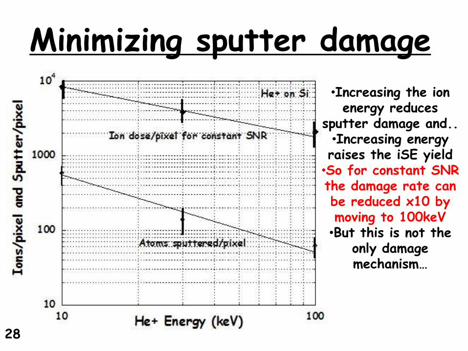
Minimizing sputter damage
•Increasing the ion energy reduces
sputter damage and..•Increasing energy raises the iSE yield
•So for constant SNR the damage rate can be reduced x10 by moving to 100keV
•But this is not the only damage mechanism…
28

High Energy He+ ion damage
•At beam energies close to the stopping power maximum (~800keV) each incident He+ ion can form impact holes in a polymer film even at low doses•This appears to be a knock-on collision (Rosenberg et al. (1962), JAP 33, 1842)
1mm

He+ radiolysis in PMMA
Dose 1.3E16 ions/cm2
Dose 4E16 ions/cm2
Dose 1.3E17 ions/cm2
Resist shrinkage 30keV He+ ionsIB 0.23pA, dwell time 30msMaximum Dose 1.3E17 ions/cm2
Shrinkage 5% @ 10 ions/A2
Manageable and predictable
Radiolysis limit for electrons ~10 el/A2

So is HIM metrology an improvement?
HIM image array of pillars 50nm spacing
HIM line trace shows <1nm resolution at top, FWHM <3nm at base 100nm lower, no tails or
defocus and minimal charging

36
FOV 100 nm
2.79 E18
5-6 nm width
Is this the future of Metrology?
Dr. Dan Pickard, Nat’l University of Singapore)
•31keV beam, Ib=0.4pA•Single layer graphene sheet –note high contrast, good SNR•10nm repeat features, 5nm FWHM – cleanly resolved with detail down to <1nm

Plus and MinusThe high resolution and great depth of field
of the HIM is ideal for device metrology
Ion dose required for acceptable SNR achieved is consistent with need for speed
Damage is comparable with e-beam case
Topographic line profiles are similar to e-beam – but care in analysis is needed
Ability to model signal profiles is limited by incomplete data base of iSE yields for elements and especially for compounds

Thank You• Thanks to Brendan Griffin (UWA); Mike Postek,Andras Vladar, John Villarubbia (NIST); and Larry Scipioni (Zeiss) for their helpful suggestions and assistance
• This work was partially supported by GRC, Program Manager Dr. D Herr
• And ..

http://cnms.ornl.gov
Center for NanoPhase Materials Science, Oak Ridge National Laboratory