Embed Size (px)
Citation preview

METAL-INSULATOR TRANSITION IN BORON-ION IMPLANTED TYPE II a DIAMOND
Tshakane Tshepe
A thesis submitted to the Faculty of Science, University of the Witwatersrand, Johan
nesburg, in fulfillment of the requirements for the degree of Doctor of Philosophy.
Johannesburg, 2000

Declaration
I declare that this thesis is my own, unaided work. It is being submitted for the degree
of Doctor of Philosophy in the University of the Witwatersrand, Johannesburg. It has
not been submitted before for any degree or examination in any other University.
(Signature of Candidate)
23rd August 2000

Abstract
High purity natural type Ila diamond specimens were used in this study. Conduct
ing layers in the surfaces of these diamonds were generated using low-ion dose multiple
implantation-annealing steps. The implantation energies and the ion-doses were spread
evenly to intermix the point-defects, thereby increasing the probability of interstitial
vacancy recombinations and promoting dopant-interstitial-vacancy combination resulting
in activated dopant sites in the implanted layers. The process used to prepare our sam
ples is known as cold-implantation-rapid-annealing (CIRA). Carbon-ion and boron-ion
implantation was used to prepare the diamond specimens, and de-conductivity measure
ments in the temperature range of 1.5-300 K were made following each CIRA sequence.
An electrical conductivity crossover from the Mott variable range hopping (VRH)
to the Efros-Shklovskii VRH conduction was observed when the temperature of insulat
ing samples was lowered. The conductivity crossover temperature Tcross decreases with
increasing concentration of the boron-ion dose in the implanted layers, indicating the nar
rowing of the Coulomb gap in the single-particle density of states near the Fermi energy.
The critical boron-ion concentration nc for the metal-insulator transition and the critical
conductivity exponent f.-£ have been estimated to be nc ~ 4.0 x 1021 cm-2 and f.-£~ 1.7.
There is, however, a fairly large uncertainty in nc since it is not absolutely certain that
all the boron ions are activated during the high-temperature annealing processes.
The importance of annealing boron-ion implanted diamond samples at high temper
atures was demonstrated in this study. A significant rise in electrical conductivity (drop
in resistivity) is reported with increasing annealing temperature. Such an increase in
conductivity may be linked to the removal of the compensating donor centres and/ or the
minimization of the lattice disorder.
ii

M adume le ditebogo ke di lebisa go ba lelapa la me, le botlhe ba ba ineetseng go direla
Modimo go ya bukhutlong jwa nako
iii
Acknowledgments
This has been a long protracted battle for me. I am therefore tempted to thank
everyone I met in the physics department for such is my relief at having completed
this thesis. Sanity dictates, though, that I should first thank my supervisor, Prof. Mike
Hoch, for his guidance, patience and encouragement throughout this project. I am indeed
grateful to have him as my supervisor. I would like to thank Prof. Johan Prins, my second
supervisor, for invaluable time and advice he provided during the course of this work.
Many thanks are due to my colleagues in the physics department. In particular, I
would like to record my appreciation to Dr. lain Goudemond for introducing me to
the cryogenic system in the Nuclear Magnetic Resonance laboratory. I would like to
thank Dr. Graeme Hill (he finished before me) and Charles Kasl for useful suggestions,
stimulating discussions during our research activities in the laboratory.
I wish to thank Mrs. Renee Hoch for proof reading this thesis, correcting my grammar,
and making sure that what I wrote actually made sense.
I am grateful for the financial assistance I received from the University.
It is with a deep sense of loss and profound sadness that my mother did not see me
graduate. Life is such. Ke rata ke leboga botlhe ba ba ileng ba ntshegetsa ka dithapelo
le dikeletso. Ammaruri Modimo o mogolo. Ke lo leboga go menagane. E kete kagiso ya
Morena, e e fetang ditlhaloganyo tshotle, e ka boloka dipelo le maitlhomo a tsone mo go
Keresite Jesu. Go weditswe.
iv

Contents
1 General introduction and research overview
1.1 Scope of this thesis . . . . . . . . . . . . . . . ................
2 The metal-insulator transition in doped semiconductors
2.1 Introduction . . . . . . . . . . . . . . . . . . . .
2.2 Anderson localization and Anderson transition .
2.3 Electron-electron interaction theory ....
2.4 Variable-range hopping conduction theory
2.4.1 Mott VRH conduction theory . . .
2.4.2 Efros-Shklovskii VRH conduction theory
2.5 Many-electron transitions in doped systems
2.6 Transport properties in the metallic regime .
2.7 The derivative method ..
2.8 Mott-Hubbard transition .
2.9 Scaling theory of localization.
2.10 Critical conductivity exponent .
2.11 Shlimak method . . . . . . . . .
2.12 Minimum metallic conductivity
2.13 Weak localization theory
3 Ion implantation
1
16
24
25
25
28
29
31
32
33
34
36
38
40
43
45
47
49
50
53
3.1 Introduction .....
3.2 General background.
53
54
3.2.1 Stopping processes of ions in a solid . 54
3.3 Implantation temperature . . . . . . . . . . 60
3.3.1 Cold-implantation followed by rapid-temperature annealing cycle 60
3.3.2 Selection of the ion energies and doses 60
3.3.3 Activation of dopant-interstitials ...
3.3.4 Behaviour of self-interstitials in the damaged layers
3.3.5 Behaviour of vacancies in ion-implanted layers
3.3.6 High-temperature implantation
3.4 Annealing studies .
3.4.1 Motivation .
3.4.2 High-temperature anneal (T ~ 770 K)
3.4.3 Low-temperature anneal (T ~ 770 K) .
3.5 Lattice swelling
3.6 Energy-loss simulation program: TRIM92
3. 7 Secondary ion mass spectroscopy (SIMS)
4 Experimental details
4.1 Introduction ....
4.1.1 Sample designation
4.1.2 Diamond shaping and polishing
4.1.3 Diamond target holder
4.2 Ion implantation .
4.3 Annealing furnace.
4.3.1 Cleaning of diamond samples and sample storage
4.3.2 Implanted boron and carbon ions dose levels
4.4 Janis cryostat ............... .
4.4.1 Maintenance of the Janis cryostat .
2
61
61
62
62
63
63
63
64
64
66
69
72
72
72
73
73
75
76
76
78
87
89

4.4.2 A procedure for the running of the Janis cryostat
4.4.3 Cryogenic sample probe . . . . . . . . . . . . . .
4.4.4 Temperature controller and the Keithley electrometer
4.4.5 Low-temperature electrical conductivity measurements
4.5 The dip measuring system .......... .
4.6 High-temperature conductivity measurements
5 High-temperature annealing results
5.0.1 Motivation ......... .
5.1 High-temperature annealing results
5.2 Theoretical model for the point-defects
5.3 Discussion . . . . . . . . . . . . .
5.3.1 Multiple CIRA sequences
5.3.2 Residual damage saturation
90
93
95
95
97
98
103
103
104
108
109
109
110
5.3.3 Activation of boron ions in implantation-damaged layers 111
5.4 Summary . . . . . . . . . . . . . . . . . . . . . . . . . . . . . . 114
6 Percolative transition in carbon-ion implanted type Ila diamond 116
6.0.1 Motivation .......... .
6.1 Introduction and a general overview
6.2 Percolation theory .
6.3 Experimental results
6.4 Discussion . . . . .
6.5 Insulating samples
6.5.1 Conduction via the nearest-neighbour hopping sites
6.5.2 Conduction by variable-range hopping mechanism .
6.5.3 Calculation of the radius of the conducting spheres
6.5.4 Calculation of Bohr radii of conducting centres.
6.5.5 Minimum metallic conductivity
3
116
117
121
123
127
127
127
128
131
132
132

6.5.6 Transport in the metallic regime.
6.6 Conclusion . . . . . . . . . . . . . . . . .
134
134
1 Electrical conductivity results of boron-ion implanted diamond 136
7.1 Introduction . . . . 136
7.2 Insulating samples 137
7.2.1 Motivation. 137
7.3 Metallic Samples . 143
7.3.1 Motivation. 143
7.4 Conduction near the M-I transition 144
7.4.1 Motivation ...
7.5 The derivative method
7.6 High-temperature measurements.
7.6.1 Motivation ........ .
144
149
149
149
8 Discussion of the electrical conductivity results for boron-ion implanted
type Ila diamond 154
8.1 Introduction . . 154
8.2 Insulating samples 155
8.3
8.2.1 Activation conduction mechanism 156
8.2.2 The derivative method for the insulating materials. 157
8.2.3
8.2.4
8.2.5
8.2.6
8.2.7
8.2.8
8.2.9
Variable-range hopping conduction ........ .
The optimum hopping distance and tunneling exponent .
A crossover between Mott andES variable-range hopping .
Coulomb gap and the crossover temperature
The unperturbed density of states . . . . . .
Mobius et al. scaling model in the VRH regime
Aharony et al. scaling law in the VRH regime
Conduction in the metallic regime .
4
162
167
169
171
174
175
176
181

8.3.1 The derivative method for the metallic systems
8.3.2 Classification of samples due to e-e interactions
8.3.3 Shlimak et al. method near the M-1 transition
8.4 Conduction at the M-1 transition .......... .
8.4.1 Mott Criterion and the minimum metallic conductivity
8.4.2 The derivative method for systems at the M-1 transition
8.5 Compensation of boron-ion impurity centres
9 Conclusions
9.1 Insulating samples ............... .
9.2 Conduction near the metal-insulator transition .
9.3 Conduction in the metallic regime
9.4 High-temperature annealing
9.5 Percolation transition .
9.6 Future Directions
9.7 Published papers
5
187
190
191
193
193
196
200
201
201
202
203
203
204
204
205

List of Figures
1-1 A schematic view of the diamond band gap, which is an indirect band gap
system[3], showing locations of impurity bands. . . . . . . . . . . . . . . 20
1-2 The critical behaviour of a(O) in uncompensated Si:P and heavily com
pensated Si:(P,B) systems. The system shows a continuous transition with
solid lines being fits to Eq. (1.6). The experimental data have been taken
from articles by Palaanen et al.[18] and Hirsch et al. [19]. . . . . . . . . 23
2-1 The figure shows the main theories which describe transport properties for
systems near the metal-insulator transition in the presence and absence of
a magnetic field. The electron concentration is represented by a horizon-
tal axis. The effects of the electron-electron interactions are divided into
three conductivity regimes: insulating, near the metal-insulator transition,
and metallic. The y-axis reflects the importance of electron-electron in
teractions in various theories. This figure has been taken from Uwe Hans
Thomanschefsky's PhD thesis[26]. an is the Boltzmann conductivity. The
other symbols are defined in the text. . . . . . . . . . . . . . . . . . . . . 27
2-2 The single-electron DOS is shown when effects due to electron-electron in
teractions are (a) neglected and (b) included in the variable-range hopping
theory. The depletion in the DOS is referred to as the Coulomb gap. . . 30
6

2-3 A schematic diagram showing the Matt-Hubbard transition brought about
by electron-electron interactions. The model used by Mott and Hubbard
ignores the effect due to disorder and the magnetic behaviour of the system.
The splitting of the top band (D-1 band) into lower and upper Hubbard
bands is due to Coulomb repulsion by intrasite electrons. At T = 0 K, the
bottom band (D band) is completely filled with one electron per site, while
the upper band is empty. The energy that separates the top band from the
lower band is the difference between the Coulomb repulsion energy U and
the bandwidth energy B, i.e., c2 = U -B. A metal-insulator transition will
occur when U = B. This situation occurs when the interatomic spacing
is systematically reduced to allow electron wavefunctions to overlap more
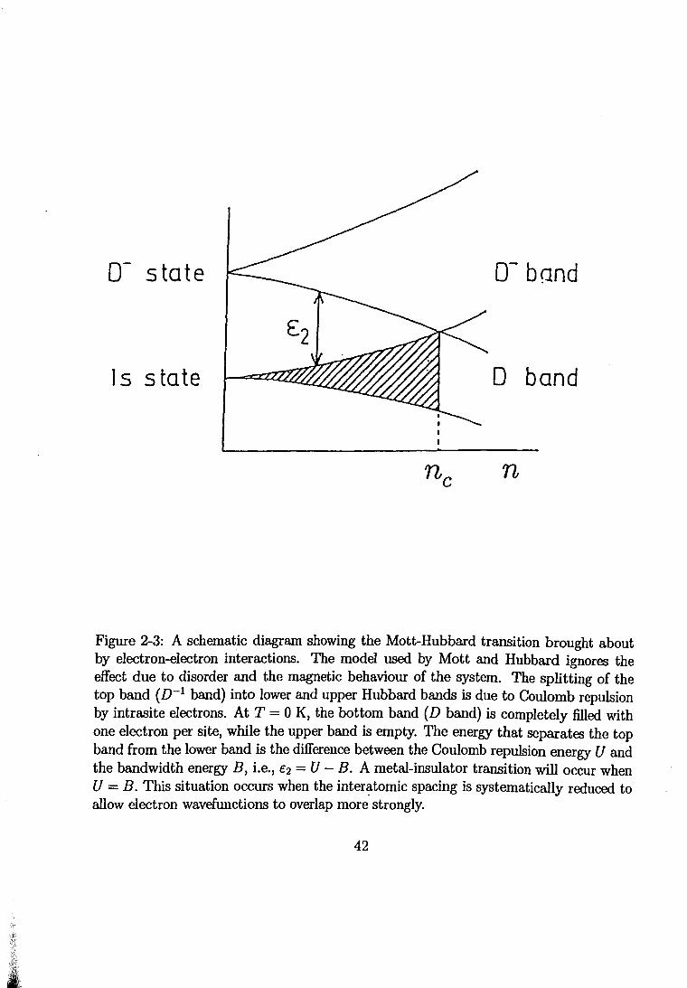
strongly. . . . . . . . . . . . . . . . . . . . . . . . . . . . . . . . . . . . . 42
2-4 Predictions of'a one-parameter scaling theory of localization are depicted
in this figure, where we have plotted the scaling function f3(g) as a function
of In (g(L)). All states are localized in !-dimensional and 2-dimensional
systems for any amount of disorder. 9c defines the critical conductance for
a 3-dimensional system. . . . . . . . . . . . . . . . . . . . . . . . . . . . 46
2-5 The diagram shows a succession of electron scattering events as the elec-
tron moves from point A to point B. An electron can be scattered around
a closed loop, as shown at point Z. In this case, phase coherence can be
maintained around the loop, resulting in a reduction in the total conduc
tivity of the system, hence the phenomenon of weak localization. The
dashed lines show the complimentary (either clockwise or anti-clockwise)
paths. These paths are referred to as the time-reversal paths. The weak
localization phenomenon can be destroyed when the temperature of the
system is increased or a magnetic field is applied to the system. . . . . . 52
3-1 A simplified schematic description of the damage cascade introduced dur-
ing the ion-implantation process. This figure is taken out of ref.[5]. . 58
7

3-2 A typical figure showing a cold-implantation damage profile of a diamond
specimen implanted with boron-ions which were accelerated into the di
amond surface at 130 keV. This profile was obtained using the TRIM-
92 computer simulation program in which the following parameters were
supplied to the program: the displacement energy, Ed = 35 eV, and the
binding energy, Eb = 5 eV. The penetration depth (projected ion range)
is given by Rp, while straggling (i.e. the standard mean deviation from
Rp) is denoted by /:1Rp. . . . . . . . . . . . . . . . . . . . . . . . . . . . . 68
3-3 SIMS profile for a square boron-ion implanted type II a diamond specimen.
The actual total dose implanted into this sample was 1.2 x 1016 cm-2. SIMS
measured the same dose as implanted. The sample was annealed at 1200
ac for 30 minutes after each implantation process. . . . . . . . . . . . . . 70
3-4 SIMS profile for a rectangular boron-ion implanted type II a diamond spec
imen. The actual dose implanted into this sample was 7.9 x 1016 cm-2
using multiple CIRA steps. The SIMS measured the boron atoms in the
implanted layer to be 7.3 x 1016 cm-2. This sample was annealed at 1200
ac for 5 minutes after each implantation process. . . . . . . . . . . . . . 71
4-1 Shown in this figure is sample A which is one of the four type II a diamond
specimens used in this thesis. The dimensions of this sample can be read
off from the figure. . . . . . . . . . . . . . . . . . . . . . . . . . . . . . . 7 4
4-2 A diagram of the annealing furnace used to anneal our diamond specimens
after the cold ion-implantation process. Samples were slid down the re
tractable chute with the implanted face down into a preheated graphite
crucible. The annealing was carried out in a pure-argon atmosphere. . . . 77
4-3 Plot of I(A) vs. V(V) to demonstrate Ohmic behaviour exhibited by a
variety of doses implanted into sample A. . . 81
4-4 A cross-sectional view of the Janis cryostat. 88
8

4-5 A simplified schematic view of the cryogenic system. The nitrogen bath is
not shown in the figure. . . . . . . . . . . . . . . . . . . . . . . . . . . . 91
4-6 A simplified schematic view of the Janis cryostat. The nitrogen bath is
not shown in the figure. . . . . . . . . . . . . . . . . . . . . . . 92
4-7 A schematic view of the cryogenic probe used to mount samples. 94
4-8 A sample holder used in the study of high-temperature conductivity mea-
surements. . . . . . . . . . . . . . . . . . . . . . . . . . . . . . . . . . . . 100
4-9 A block diagram of the conductivity setup for high-temperature conduc
tivity measurements. . . . . . . . . . . . . . . . . . . . . . . . . . . . . . 102
5-1 Plots of electrical resistance vs. cumulative boron-ion dose. Samples have
been annealed at 1200 oc for 5 minutes. . . . . . . . . . . . . . . . . . . 105
5-2 Plots of R vs. T for sample AB81. This sample was annealed over various
temperatures shown in the figure. . . . . . . . . . . . . . . . . . . . . . . 106
5-3 Plots of R vs. T for sample AB84. This sample was annealed only at 1700
oc after the CIRA routine. . . . . . . . . . . . . . . . . . . . . . . . . . . 107
5-4 Plots of R vs. 1/T for sample DB12 (square sample) annealed at 1300 oc, 1500 oc and 1700 °C. . . . . . . . . . . . . . . . . . . . . . . . . . . . . . 113
6-1 The resistivity data of Hauser et al. [144] described by the Mott VRH
relation over the temperature range 20-300 K. . . . . . . . . . . . . . . . 120
6-2 Plots of electrical resistance against temperature for various carbon-ion
implanted diamond specimens. Symbols and sample designations are given
in the figure. . . . . . . . . . . . . . . . . . . . . . . . . . . . . . . . . . . 124
6-3 Plots of R vs. r-m (m = 1/4 and 1/2) to determine which of the VRH
laws best describe the experimental data. . . . . . . . . . . . . . . . . . . 125
9

6-4 The Zabrodskii-Zinov'eva plot to determine m. Due to the sensitive depen
dence of the electrical conductivity on the carbon-ion dose in the narrow
percolation regime studied, the results were found not to be reproducible.
The carbon-ion doses implanted into the diamond samples are listed in
the figure. . . . . . . . . . . . . . . . . . . . . . . . . . . . . . . . . . . 126
6-5 The vacancy-related conducting graphite regions in carbon-ion implanted
diamond specimens have been assumed to have a spherical shape[128, 143],
but the actual shapes of these graphitic clusters are shown around the
spheres. . . . . . . . . . . . . . . . . . . . . . . . . . . . . . . . . . . . 133
6-6 The conductivity plots for samples which may be classified as metallic. 135
7-1 The resistance against temperature for a number of boron-ion implanted
type II a diamond specimens. . . . . . . . . . . . . . . . . . . . . . . . . . 139
7-2 Resistance of eleven insulating diamond specimens plotted as a function
of r-m (K-m) (where m = 1/4 and 1/2) on a semilogarithmic scale. . . . 141
7-3 a vs. T for sample AB27. A solid line through the experimental data
represents a fit to the conductivity expression: a(T) = a0 exp [- (T0 /T)m]
where m rv 0.5. . . . . . . . . . . . . . . . . . . . . . . . . . . . . . . . . 142
7-4 The electrical conductivity for some of the metallic samples plotted as a
function ofT. Samples have been annealed isochronally (10 minutes) at
various temperatures ranging from 1200 oc to 1700 °C. Symbols shown
represent: •-sample AB84 (1700 ac anneal); 6-AB81 (1700 ac anneal);
•-AB78 (1700 ac anneal); ~-AB81 (1200 ac anneal) +-AB78 (1200 ac anneal). All samples have been annealed for 10 minutes. . . . . . . . . . 145
7-5 Electrical conductivity vs. T for sample AB81. This sample has been
annealed at 1700 ac. . . . . . . . . . . . . . . . . . . . . . . . . . . . . . 146
7-6 Electrical conductivity vs. T for sample AB84. This sample has been
annealed at 1700 °C. . . . . . . . . . . . . . . . . . . . . . . . . . . . . . 147
10

7-7 Temperature-dependent electrical conductivity vs. T for samples AB78,
AB81 and AB84. A closer inspection of the plots reveals that a(T) vs. T 113
gives a better fit to the experimental data than a(T) vs. r-112 . Plotted
here are samples annealed at 1700 oc for 10 minutes. Sample AB84 is
shown in Fig. 7-8(b). . . . . . . . . . . . . . . . . . . . . . . . . . . . . 150
7-8 Plots of activation energy W = 8lna/ ln T against T. This sample, AB81,
is close to the M-I transition. According to the derivative method, sample
AB81 is weakly insulating. One of the curves fitted with a solid line has
been annealed at 1700 oc, which is the highest temperature at which
we can safely anneal our samples. The annealing temperatures for these
samples are shown in the figure. The duration of the anneal for all samples
was set to 10 minutes. . . . . . . . . . . . . . . . . . . . . . . . . . . . . 151
7-9 Plots of R(T) vs. r-m for sample AB84 measured in the temperature range
300-773 K. The insert shows the same experimental data plotted against
r-1/ 4 to check whether Mott VRH conduction applies in this temperature
range. . . . . . . . . . . . . . . . . . . . . . . . . . . . . . . . . . . . . . 153
8-1 Plots of R vs. 1/T for a number of insulating samples. Only the data
above 400 K may be used for the calculation of the activation energy, EA. 158
8-2 Plots of R(T) vs. r-m (m = 1; 1/4 and 1/2) for a high insulating sample
CB5 measured in the temperature range 300-773 K. . . . . . . . . . . . . 159
8-3 The derivative method and the White-MacLachlan method were used to
generate these plots in an effort to determine the hopping exponent m.
Samples plotted here lie in the boron-ion concentration range: 1.0- 1.9 x
1021 cm-3 . The values of the fitted slopes, which are close to the theoretical
predicted exponents of 1/2 and 1/4, are shown in the plots. . . . . . . . . 163
11

8-4 The derivative method and the White-MacLachlan method used to gener
ate plots shown in an effort to determine the hopping exponent m. Samples
lie in the boron-ion concentration range: 2.0- 3.0 x 1021 cm-3 . The fitted
slopes close to the theoretical hopping exponent of 1/2 are shown in the
plots. . . . . . . . . . . . . . . . . . . . . . . . . . . . . . . . . . . . . . . 164
8-5 The derivative method and the White-MacLachlan method used to deter
mine the hopping exponent m. Sample AB78 (n ~ 4.0 x 1021 cm-3) is
shown. Solid lines shown in the plots correspond to theoretical slopes of
-1/3 and -1/2. From the plots, a slope of -1/3 gives a better fit to the
data compared to a slope of -1/2. The annealing temperatures for this I
sample are shown in the table alongside this figure. . . . . . . . . . . . . 165
8-6 This plot demonstrates the relationship between the Mott and ES charac-
teristic temperatures in the VRH regime. . . . . . . . . . . . . . . . 173
8-7 Plots of ln a vs. r-112 for boron-ion implanted diamond specimens. The
scaling parameter a1 is shown in the figure. . . . . . . . . . . . . . . 177
8-8 Plots shown in Fig. 8. 7 can be collapsed into a single universal curve using
a1 as the scaling parameter. We have plotted data corresponding to doses
3.0- 4.2 x 1016 cm-2. Details of the method can be found in papers by
Mobius et al.[32]. . . . . . . . . . . . . . . . . . . . . . . . . . . . . . . . 178
8-9 Plots of TEs versus n in semilog and linear scales. The TEs values were
obtained with the hopping exponent fixed tom= 1/2 and a1 read from
Fig. 8.7. ...................................
8-10 Universal scaling function crossover plot of scaled resistance versus the
scaled temperature for some insulating diamond specimens. The method
179
used to generate this plot is given by Aharony et al.[200]. . . . . . . . . . 183
8-11 Electrical conductivity for one of the metallic samples, AB84, which has
been annealed at 1700 °C. . . . . . . . . . . . . . . . . . . . . . . . . . . 185
12

8-12 a(T) vs. n for samples AB78, AB81 and AB84. These samples have been
implanted close to the M-1 transition. We obtained J.-L "' 1.7 and ao =
9736 (0-cm)-1 from the fit of Eq. (1.1). The values of n have been
estimated using the SIMS technique with an error of 5 - 10 % . . . . . . 186
8-13 Following the work of Watanabe et al. [178), we can further classify sample
AB78 (curve A) as insulating, but AB81 (curve B) may taken as 'weakly'
metallic with a finite conductivity at T = 0 K. Sample AB84 is represented
by curve C. . . . . . . . . . . . . . . . . . . . . . . . . . . . . . . . . . . 192
8-14 Shlimak et al.[16] method to determine the critical conductivity exponent
f-L· We have calculated the J.-L value to be "' 1.7. The procedure for the
calculation of J.-L is outlined in the text. . . . . . . . . . . . . . . . . . . . 195
8-15 Edwards-Sienko plot [79) demonstrating the Mott criterion. The <>C:B
sample that we have studied is shown against other doped semiconductors
in this figure. . . . . . . . . . . . . . . . . . . . . . . . . . . . . . . . . . 197
13

List of Tables
4.1 Implantation energies and ion doses used in this study. The accelerating
energies and doses were spread into small steps to generate highly con
ducting boron-ion and carbon-ion layers in the diamond samples. 79
4.2 Energy, boron-ion dose and carbon-ion fl.uences used to generate Ohmic
contact regions on the diamond surfaces. The electrical contacts are spaced
about 5.5 mm apart. . . . . . . . . . . . . . . . . . . . . . . . . . . . . . 82
4.3 Summaries of boron-ion and carbon-ion implanted type lla diamond sam
ples (insulating samples) used in this study, and their characterizations
are given in table 4.3-4.6. . . . . . . . . . . . . . . . . . . . . . . . . . . . 83
5.1 Ion energies and ion doses used to generate a boron-ion layer in a diamond
specimen. The created point-defects are homogeneously distributed in the
implanted layer. The vacancies created following each implant have been
calculated using the TRIM-92 simulation code in which the displacement
energy of 35 e V and the lattice binding energy of 5 e V were assumed. . . 112
6.1 A list of values for some variables determined from the experimental data
using the VRH relations. . . . . . . . . . . . . . . . . . . . . . . . . . . . 130
14

7.1 The Minuit least squares fitting procedure was used to determine values for
the characteristic temperatures in the Mott and the ES VRH regimes. The
uncertainty in the characteristic temperatures were estimated by fitting the
regression lines over various temperature regions in which the Mott and
the ES laws apply. The non-monotonic decrease in TM and TEs may be
an indication of the unreliability of this method . . . . . . . . . . . . . . 140
7.2 Variables of boron-ion implanted diamond obtained from the metallic ex
pression are presented in this table. . . . . . . . . . . . . . . . . . . . . . 148
8.1 Values of variables determined using electrical conductivity expressions
are described in the text. The error estimates for TM and TEs were given
in table 7.1. . . . . . . . . . . . . . . . . . . . . . . . . . . . . . . . . . . 160
8.2 Values for quantities associated with the conductivity theory are listed in
this table. Error estimates associated with the characteristic temperatures
have been given in table 7.1. The non-consistency in the Tc9
= !109/kB
(K) values seems to cast some doubts on the reliability of the VRH model
over the temperature ranges that we have investigated. . . . . . . . . . . 172
8.3 Quantities extracted using the method of Aharony are summarized in this
table. . ................................... .
8.4 Values for a-(0) are calculated from one conductivity data point for each
different sample using Eq. (8.39). These values are compared to those
182
a-(0) values obtained using the extrapolation procedure. . . . . . . . . . . 188
8.5 The a values, shown in the last column, have been calculated using Eq.
(8.44) for some samples located close to the metal-insulator transition. The
a values were found to increase as annealing temperatures were increased.
This is an indication that samples may be driven into the metalic phase
by annealing them at high temperatures. . . . . . . . . . . . . . . . . . . 194
8.6 A comparison of values of parameters obtained from OC:B and those of
the Si:B semiconductor system. .................... 198
15

Chapter 1
General introduction and research
• overview
Diamond is one of the two most common crystalline allotropes of carbon. The other
is graphite. Between these two allotropes lie a whole variety of carbon materials, ranging
from amorphous sp2 bonded carbon (such as thermally evaporated carbon, and glassy car
bon) to amorphous sp3 bonded carbon, which is structurally analogous to amorphous sil
icon and is formed during low-energy carbon-ion deposition[!]. Diamond is a metastable
form of carbon in which the atoms are equidistantly spaced at the corners of a regular
tetrahedral lattice structure. The carbon atoms are held together by strong covalent sp3
bonds. The close packing of the carbon atoms in diamond makes it a relatively dense
material.
Natural and synthetic diamond single crystals have been the subject of intensive rc:r
search for decades. The research has been driven by the excellent and often unsurpassed
properties that diamond enjoys over other materials. Diamond possesses a unique com
bination of highly favourable technological properties that puts it in a class of its own.
The history and the use of diamond have been documented in a book by Tolansky[2].
16
Some of the basic properties that put diamond in a class of its own are stated below.
• Diamond is optically transparent to electromagnetic radiation over a wide spectral
range, from a 220 nm wavelength in the ultra-violet to the far infra-red.
• Diamond enjoys the highest thermal conductivity at room temperature of all known
materials.
• Diamond's thermal conductivity is a factor of five greater than copper and a factor
of about ten greater than commonly used thermal conductive insulators.
• At ambient temperatures, diamond has a relatively low specific heat capacity, with
a Debye temperature of 2200 K, and therefore diffuses heat efficiently in transient
applications in which the speed of heat transfer is important.
• Diamond exhibits one of the lowest coefficients of thermal expansion, which en
hances the resistance to thermal shock.
• Diamond remains inert to aggressive acids and bases, and all types of chemical
reagents, even at fairly high-temperatures. It therefore offers protection in most
severe corrosive environments.
• It is one of the hardest (though brittle) known materials, and has a relatively low
coefficient of friction, ensuring a wide range of applications in cutting tools and
wear-resistant parts.
• Being a wide-band gap material (with a band-gap energy of rv5.4 eV), diamond can
be an electrical insulator. High carrier mobility opens attractive avenues for the
application of diamonds in electronic devices and radiation detectors on particle
accelerators.
17

Further articles on diamond properties can be found in a recent book by Field [3] and
references cited therein. These properties have been put to use to some extent in the
semiconductor and optical industry. See Prins [4] for a recent review article.
The generation of conductive surface layers in diamond, by means of ion implanta
tion, has conclusively been demonstrated and extensively reported in the literature[5].
The study has now matured to the stage that boron-ion layers, which have electrical
properties closely matching those that are found in natural semiconducting type lib di
amond specimens, can selectively and reproducibly be generated in a type IIa diamond
surface. In order to achieve the best results for boron doping, an implantation-annealing
scheme was devised and developed by Prins [6, 7]. It is known by the acronym CIRA
(cold-implantation-rapid-annealing), and is discussed in chapter 3. The CIRA technique
involves implanting samples at low temperatures to inhibit the diffusion of the point
defects in the damaged layer, followed by rapid high-temperature annealing to reduce ra
diation damage and to drive the dopants into the electrically active substitutional sites.
At low temperatures, the electronic properties of doped semiconductors are generally
determined by impurities. An impurity can either be a donor or an acceptor, accord
ing to its location in the periodic table relative to the host material. Diamond is a
covalently bonded group IV insulator. The group III elements are said to be p-type
dopants (acceptors) in diamond. Boron, in particular, makes a good dopant since its
volume is comparatively close to that of the carbon atom, and boron atoms may occupy
substitutional sites after high-temperature annealing.
A characteristic property of an acceptor impurity is its ability to capture an electron
from the target material, leaving a hole to conduct electrically. The impurity centre
becomes negatively charged by virtue of an electron it has trapped, while a hole appears
in the valence band. Since the resulting hole has a positive charge, it is attracted by the
18

acceptor. An acceptor (donor) is said to be of a shallow type if its energy level lies close
to the valence (conduction) band, that is, when the ionization energy (energy required
to excite an electron from the top of the valence band to fill the hole) is much smaller
than the band-gap energy. A schematic view of the diamond band gap showing locations
of impurity bands is given in Fig. 1-1.
Each impurity inserted into a host contributes a discrete local energy level into the
forbidden energy band gap. As more and more impurities of a particular type are ran
domly introduced into the host, their wavefunctions overlap more strongly. The acceptor
(donor) energy levels eventually merge and broaden into a band, known as an impurity
band. The electrons delocalize and the system transforms into a metallic phase. At
low-dopant concentration, the overlap of the electronic wavefunctions of impurities is
small, and hopping electrical conduction between spatially distinct localized impurity
sites occurs, mediated by phonons.
Insulators are characterized by thermally activated electrical conduction with a van
ishing conductivity at absolute zero temperature, while metals exhibit a finite zero tem
perature conductivity, a-(0). In order to distinguish a metal from an insulator, one there
fore needs to measure the electrical conductivity as a function of temperature and then
extrapolate the results to T = 0 K to check for the behaviour of a-(0). This procedure
involves some optimization of parameters controlling the transition. The exact nature of
the M-I transition in doped semiconductors has been the subject of much interest since
the 1960's and continues to receive intense experimental and theoretical focus. Some of
the well-studied disordered systems include silicon and germanium.
The basic concepts behind the theory of the M-1 transition, which extend beyond
the band theory, were introduced by Mott[8], who studied the effects of electron-electron
interactions, and by Anderson[9], who pointed out the importance of lattice potential
19

- -
CONDUCTION BAl'ID
- -4eV
- -
1.7 eV
• Substitutional nitrogen donor
Possible vacancy associated - donor centres
I
0.37 eV I Substitutional boron acceptor level
VALENCE BAND
Figure 1-1: A schematic view of the diamond band gap, which is an indirect band gap system[3), showing locations of impurity bands.
20

disorder in a non-periodic system. Electron-electron ( e-e) interactions and disorder are
complex phenomena difficult to deal with even when treated separately. Their interplay
has complicated what can be perceived as an already complex situation, making transport
studies interesting but difficult to explain in detail. It should be pointed out that no
complete theory, which incorporates the effects of both electron-electron interactions and
disorder on an equal footing, particularly near the M-1 transition, is available.
An important question still being debated is whether the electrical conductivity drops
abruptly to zero at the critical concentration nc, or is a continuous function of dopant
concentration as the M-1 transition is approached from either side of the transition, be it
metallic or insulating. Mott, using the loffe-Regel (IR) criterion[lO], argued for the dis
continuity in the electrical conductivity at the transition. The IR criterion crudely states
that no electrical conductivity will occur when the mean free path between the scattering
events is smaller than the interatomic spacing. The scaling theory of localization pro
posed by Abrahams et al. [11] predicts a continuous transition at nc. This debate, though
adding some impetus towards the understanding of the transport problem in doped sys
tems, managed for a while to polarize researchers in the field into two opposing camps.
One group, championed by Mott, argued for the occurrence of the minimum metallic
conductivity CJmin· Although Mott was later persuaded to accept that CJmin does not exist,
Mobius et al.[12, 13, 14] have come out recently in support of CJmin· Accepting that the
behaviour of CJ(O) is continuous at the localization threshold, the critical behaviour may
be described using a critical exponent J..L as follows[15]:
(}(0) = (}0 ( ~ - 1) ~ (1.1)
with (} 0 being the parameter which controls the conductivity scale. A wide range of
J..L values have been found by a number of authors in various systems which undergo the
M-1 transition[15]. The reader is referred also to the recent interesting results of Shlimak
et al.[16] and to contrasting arguments presented by Sarachik and Bogdanovich[17]. Fig.
21

1-2 shows the critical behaviour of O"(O) in the phosphorus doped silicon system, Si:P,
measured by Rosenbaum et al.[18] and the behaviour of O"(O) in Si:(P,B) determined by
Hirsch et al.[19]. The system shows a continuous transition, with solid lines being fits to
Eq. (1.1).
The M-I transition, which occurs as a function of dopant concentration, is the main
subject of the present investigation in boron-ion implanted type IIa diamond. The tem
perature range of interest is 1.5-300 K. The electrical conductivity measurements were
extended up to 773 K.
Electrical conductivity studies have also been carried out in boron-ion doped CVD
diamond polycrystalline crystals by a number of authors[20, 21]. A review article which
covers the growth, application and electrical conductivity properties has been published
recently by Werner and Locher[22]. The conductivity results obtained in CVD diamonds
are consistent with those obtained in implanted natural single-crystalline diamonds.
Besides the study of the electronic properties of boron in natural diamond in this
thesis, we have also studied the percolative nature of electrical conduction in carbon-ion
implanted diamond. The carbon-ion work may be regarded as a preliminary step in the
M-I project.
22

300
250 a· Si:P "' Si:(P,B) •
~ ..- 200 I
E (.)
...... 150 I c ....._.,
,.-.... 0 100 ....._., b
50
0 3 4 5 6 7 8 9
Figure 1-2: The critical behaviour of u(O) in uncompensated Si:P and heavily compensated Si:(P,B) systems. The system shows a continuous transition with solid lines being fits to Eq. (1.6). The experimental data have been taken from articles by Palaanen et
al.[18] and Hirsch et al. [19].
23

1.1 Scope of this thesis
Chapter 2 summarizes the main concepts applied to the study of the metal-insulator
transition, reviewing the major approaches to the transport problem and focusing on
recent developments. The ion implantation theory is discussed in chapter 3. Chapter
4 describes sample characterizations and the cryogenic apparatus used in the electrical
conductivity studies. The work on carbon-ion implanted type Ila diamond is presented
in chapter 5. Chapter 6 is devoted to the results obtained using the CIRA technique.
Various annealing cycles were employed in order to achieve substitutionally B-doped dia
mond with as few other defects present as possible. Chapter 7 presents the conductivity
results obtained in the temperature range of 1.5-773 K, while chapter 8 provides an
analysis of the results in the light of recent theories. Chapter 9 gives a summary of all
the results, offers some comments on the unresolved problems in this field, and suggests
some possible areas for future research.
24

Chapter 2
The metal-insulator transition in
doped semiconductors
2.1 Introduction
In this chapter, a large body of experimental and theoretical work on the study of the
metal-insulator (M-I) transition in disordered systems is surveyed. There is an extensive
literature on the subject, with an excellent introductory text written by Mott[8]. Other
reviews are given by Shklovskii and Efros[23], Bottger and Bryksin[24] and Belitz and
Kirkpatrick[25]. The last of these covers the state of the M-I theory on both sides of
the transition in depth. Since most of the experimental work in this thesis has been
performed on samples located on the insulating side of the transition, only a brief outline
of those theories which describe the details of the transport properties in the metallic
regime will be given. Some of the models pertinent to the study of the M-I transition
are summarized in Fig. 2-1[26]. Not all of these theories are discussed in this chapter,
but can be found in references cited above.
25

The problem of the M-1 transition has been addressed theoretically from either of
the two conductivity limits: metallic or insulating. The interpretations of the experi
mental data have been based mainly on extrapolations using the two-parameter power
law expression, (J'(T ----+ 0, x) = a + CTP, where x stands for a dopant impurity con
centration, and p = 1/2 or 1/3 in the case of metallic samples. On the insulating side
of the transition, a = 0, and (]' ----+ 0 as T ----+ 0 K. FUrther work on systems which un
dergo M-1 transitions has been discussed recently by Rosenbaum et al.[27, 28, 29, 30].
A power law approximation, however, involves several assumptions and uncertainties,
casting some doubt on the reliability of the extrapolated results[12, 31, 32, 33, 34, 35].
Nevertheless, the predictions of some theories, particularly those which incorporate the
effects of electron-electron interactions and disorder, have been confirmed near the crit
ical concentration, nc, by a number of authors to a high degree of accuracy[36]. Quite
recently, Shlimak and co-workers[16] have proposed a method to determine nc and the
conductivity critical exponent 1-£ without extrapolating (J'(T) to zero temperature. The
method is based on the assumption that the log (J'(T) vs. T curves are parallel for n ,2:: nc.
This may not be a good assumption. The Shlimak et al. [16] method is discussed in a
later section in this chapter.
On the insulating side of the transition, a general conductivity relation, (J'(T) =
(]'1 exp [- (¥) m] , describes transport behaviour in the variable-range hopping (VRH)
conduction regime adequately[8]. An exponent of m = 1/4 is associated with negligible
electron-electron interaction and non-changing density of states (DOS) near the Fermi
energy (EF ), while m = 1/2 signifies VRH hopping in the strong Coulomb regime[23].
More details on transport properties on the insulating side will be given later in the
chapter.
The two main ingredients in the study of M-1 transitions are disorder and electron-
26

DISORDER
i ! i
I I
OISORC;:R : I i
AND I I
INSULATING n<nc
Variable Range
Hopping
Coulomb Gap
H-
TRANSITION n =nc
Anderson Transition
ScaJing Theory of
Localization
•Modem• Scaling Theories
METALLIC n>>nc
Weak LocaJization
i I ! : : ----·------!
a<oa i
6a{T)=BT314. I :
oo(H) >0 i ! !
I i I I
I I : I
!
flda(T}=mT112 If
Figure 2-1: The figure shows the main theories which describe transport properties for systems near the metal-insulator transition in the presence and absence of a magnetic field. The electron concentration is represented by a horizontal axis. The effects of the electron-electron interactions are divided into three conductivity regimes: insulating, near the metal-insulator transition, and metallic. They-axis reflects the importance of electron-electron interactions in various theories. This figure has been taken from Uwe Hans Thomanschefsky's PhD thesis(26]. (J"B is the Boltzmann conductivity. The other symbols are defined in the text.
27

electron ( e-e) interactions (also referred to as electron correlations). Both have proven
to be very complex phenomena even when treated separately and independently of each
other, but their contributions may be of comparable importance and their effects inter
twined. As stated in chapter 1, there is no complete theory available which incorporates
the two phenomena on equal footing up to this stage. Their influence on systems which
undergo the M-1 transition are discussed separately.
2.2 Anderson localization and Anderson transition
Spin localization, independent of the effects of electronic interactions, was predicted
by Anderson in his 1958 classic paper, entitled "Absence of diffusion in certain random
lattices", using the tight binding approximation model(9J. He showed that the electronic
wavefunctions can become localized in an array of potential wells if sufficient disorder is
introduced. The disorder here is introduced by letting the lattice potential due to the
randomly incorporated impurity atoms fluctuate from site to site in space. An electron
moving through a series of nonidentical potential wells, fluctuating randomly in depth
(on-site energies) by a certain amount, can be localized. Taking the size of potential
variation to be ± W /2, where W is the energy of disorder, Anderson showed that an
electron can stay localized at a particular impurity site when the ratio of W to the
bandwidth (electron overlap) B = 2zV exceeds a critical value, eDcrit' where z is the
coordination number and V is the potential. This kind of localization, caused solely by
disorder, is referred to as Anderson localization.
The transition that takes place as a result of the variation of disorder in a doped semi
conducting system is referred to as an Anderson transition. Bottger and Bryksin(24] and
Shklovskii and Efros(23] have presented reviews on the Anderson subject in a scholarly
28

fashion, and this will not be laboured further.
2.3 Electron-electron interaction theory
Long-range electron-electron (e-e) interactions have a profound influence on the elec
tronic and thermodynamic properties of disordered systems, particularly in the localized
(insulating) regime. In the latter regime, the e-e interactions give rise to a depletion in
the single-electron density of states (DOS) near the Fermi energy Ep. This depletion re
gion, which may be parabolic in shape, is referred to as a Coulomb gap ( Cg) [37]. The Cg
is sketched in Fig. 2-2. The theory, manifestation and influence of the Cg on transport
properties can be found in standard M-1 transition books. The reader is referred here to
books by Shklovskii and Efros[23] and Bottger and Bryksin[24].
The first theoretical papers on the pronounced influence of the Coulomb interaction
on the DOS near the Fermi energy appeared about three decades ago. Pollak[38] and
Srinivasan[39] showed, using analytical studies, that the DOS exhibits a minimum near
Ep. Such an observation was made when they tried to stabilize the ground state with
respect to one-electron transitions. Their observation was later confirmed numerically by
Kurosawa and Sugimoto[40, 41]. Efros and Shklovskii[42] pointed out that the long-range
tail of the unscreened Coulomb interaction induces a pseudogap in the DOS near Ep.
The role of the Cg, particularly in transport studies, is still embroiled in controversy up
to this date[43], the main source of controversy being the type of the density of states to
which the Cg applies. The single-electron density of states can be defined as the number
or concentration of localized states, which lie near the chemical potential, per unit energy
and unit volume, in which an added electron will increase the energy of the system by
E when no other electrons are allowed to move from their original positions[44]. It is
29

g (E)
( a )
g (E) (b)
Ef +E'max E
Figure 2-2: The single-electron DOS is shown when effects due to electron-electron interactions are (a) neglected and (b) included in the variable-range hopping theory. The depletion in the DOS is referred to as the Coulomb gap.
30

worth noting that the Cg does not apply to the many-body thermodynamic density of
states which characterizes the density of total system excitations. A detailed review
of the e-e interactions in disordered systems can be found in ref.[44]. The reader is
referred to chapters 4 and 5 in this book. A great deal of work on the subject has
been carried out by a number of authors. Literature on the M-1 transition and related
transport phenomena is growing at a bewildering rate, making tt extremely difficult to
keep abreast of the new developments. This could well reflect on the amount of interest
this field generates. For an up-to-date review on the subject, the reader is referred to
recent articles by Rosenbaum et al.[27, 30] and Imada et al.[45]. Further references on the
subject can be found also in a paper by Massey and Lee[46], and conference proceedings
in Hopping and Related Phenomena [47] and Metal-non-Metal Transition in Macroscopic
and Microscopic systems[48].
2.4 Variable-range hopping conduction theory
Variable-range hopping (VRH) theory has been quite successful in describing trans
port properties in disordered systems. Early theoretical ideas were proposed by Mott[49].
Others built on these ideas, with notable contributions made by Ambegaokar et al. [50],
who used percolative models to arrive at the same results as Mott. Shklovskii and Efros
(ES) have given an extensive review of the theory in their book, Electronic Properties of
Doped Semiconductors[23]. I present a summary of both the Mott VRH andES VRH
models below.
31
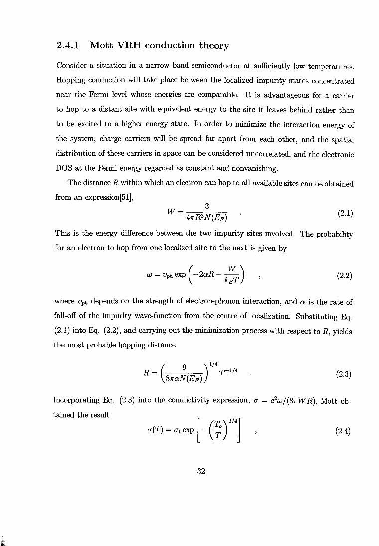
2.4.1 Mott VRH conduction theory
Consider a situation in a narrow band semiconductor at sufficiently low temperatures.
Hopping conduction will take place between the localized impurity states concentrated
near the Fermi level whose energies are comparable. It is advantageous for a carrier
to hop to a distant site with equivalent energy to the site it leaves behind rather than
to be excited to a higher energy state. In order to minimize the interaction energy of
the system, charge carriers will be spread far apart from each other, and the spatial
distribution of these carriers in space can be considered uncorrelated, and the electronic
DOS at the Fermi energy regarded as constant and nonvanishing.
The distance R within which an electron can hop to all available sites can be obtained
from an expression[51],
W= 3 41rR3N(EF) (2.1)
This is the energy difference between the two impurity sites involved. The probability
for an electron to hop from one localized site to the next is given by
w = Vphexp ( -2aR- k:T) (2.2)
where vph depends on the strength of electron-phonon interaction, and a is the rate of
fall-off of the impurity wave-function from the centre of localization. Substituting Eq.
(2.1) into Eq. (2.2), and carrying out the minimization process with respect toR, yields
the most probable hopping distance
R- 9 r-1/4 ( )
1/4
- 81raN(EF) (2.3)
Incorporating Eq. (2.3) into the conductivity expression, a = e2wj(81rW R), Mott ob
tained the result
<1(T) = <11 exp [- (~) lf'] (2.4)
32

where To - T M is the characteristic temperature in the Mott regime, given by
(2.5)
k B is Boltzmann constant, e = 1 I Q is taken as a measure of the radius of the localized
impurity electron wavefunction, and Na(EF) is the number of localized electron energy
states per (cm3 eV) at the Fermi energy. A full derivation of the Mott VRH law (Eq.
(2.4)) can be found in Hamilton's paper[52].
Let me summarize the main assumptions leading to the derivation of the Mott VRH
law:
• The DOS should be taken as a constant or slowly varying function of energy, and
must remain nonzero at the Fermi energy.
• Effects due to electron-electron interactions should be ignored.
• The temperature of the system must be sufficiently low enough so that phonon
assisted hopping occurs between impurity sites whose energies are not very different.
This holds for well-separated impurity sites.
• A hop from site i to an empty site j should not depend on whether a site close to
j in space is occupied or not.
2.4.2 Efros-Shklovskii VRH conduction theory
ES incorporated effects due to electron-electron interactions into the Mott scenario, and
showed that the DOS should have an analytic form[42],
(2.6)
33

where A is a proportional constant and d is the dimensionality of the system. If E' =
E- Ep, then N(E') rv jE' j2 in 3-dimensions corresponding to a 'soft' parabolic gap with
N(O) = 0. The change in the DOS at the Fermi energy has a profound influence on
the transport properties of doped and disordered semiconductors, modifying the Matt
VRH exponent from 1/4 to 1/2. In the ES case, the temperature-dependent electrical
conductivity takes the form:
a(T) ~ a2 exp [- (T;s) 112
] (2.7)
with
(2.8)
The prefactors, a 1 and a2, are marked with different subscripts because they apply to dif
ferent temperature regimes. Experimental results which exhibit a(T) ex: exp(T -l/2) are
common, and are now interpreted in terms of the Cg model [47, 53, 54, 55].
2.5 Many-electron transitions in doped systems
There are other forms of excitations of the charge-carriers that can also take place
when the temperature of the system is sufficiently low. Th~e excitations are gener
ally referred to as many-electron transitions. In most cases, the system should be in
the millikelvin-temperature range for one to observe these excitations. The motion of
electrons are described as correlated since
• the hopping probability of the electron depends on the previous hops of other elec
trons in the neighbourhood. This type of hopping has been referred to as successive
or sequential correlated hopping[56], process A[57] or adiabatic hopping[58].
34

• Correlation in motion of electrons may be inherent in the many-electron impurity
system. This effect is referred to as quantum correlation. Details of quantum
correlations can be found in a review article by Pollak and Ortuno[44].
• In some situations, several electrons participate in a single-hopping transition.
What happens here is that electrons hop to other localized impurity sites when, for
example, electron a moves from site i to site j which are far apart. The distance
that each electron covers is small compared to the distance travelled by electron a.
Such a process is referred to as correlated multi-electron hopping. This process is
more important in our case than the first two, and is further described below.
At very low temperatures (below which Matt andES VRH are not observed), electrons
behave as polarons or quasi-particles because they are considered to be "dressed-up". The
dressing consists of a polarization cloud that an electron drags along as it moves from one
site to the next. Due to this dressing, the energy of the system is much less in comparison
to the same system where excitations are effected by unscreened electrons[59}.
Studies have revealed that at sufficiently low temperatures, the low-energy polaron
excitations, following the long-range electron hopping process, cause a complete vanishing
of the DOS within a Cg. The result is a hard gap (hg) where the DOS is effectively zero
over a finite range of energy within a Cg(60, 61, 62, 63, 64]. Transitions across the hg
lead to the conduction mechanism of the form
a(T) ex exp ( -Th9 /T) (2.9)
where Th9 is the "hg" characteristic temperature. An hg is always much narrower in
variation than IE- EF j2of the soft Cg, irrespective of the system disorder. Two types
of hard gaps are known to occur in disordered systems at low temperatures. These are
magnetic hard gaps and electrical hard gaps. The manifestations of magnetic hard gaps
35

I
are due to the interactions of the magnetic moments of the spins[65, 66), and have been
found to be temperature- and magnetic field- dependent. It has been observed in several
materials, such as CdMnTe:In[66), that the magnetic hard gap transforms into a soft
gap under strong magnetic fields, with the exponent of unity changing to a 1/2. The
temperature range in which the hg phenomenon has been observed is 300 mK-2 K. In
contrast to the origin of the magnetic hard gaps, electrical hard gaps have been found
to be insensitive to an external magnetic field. Typical examples which have been well
studied include In/InO:~ composite films, which retain the hopping conductivity exponent
of unity up to 8 T over the temperature range 7-35 K, exhibiting hard gap phenomena[53).
2.6 Transport properties in the metallic regime
Effects of electron-electron interactions in dirty (or disordered) metals have tradi
tionally been treated within the framework of Fermi liquid theory. A dirty metal is
described as one in which the scattering mechanisms of the conduction electrons by sta
tic local impurities are strong, but not sufficient to localize the electronic eigenstates.
In the Fermi liquid theory, no anomaly in the behaviour of the DOS is expected. Al't
shuler and Aronov[67], using diagrammatic techniques, have shown that the effects of
electron-electron interactions in dirty metals give rise to a dip (sometimes referred to as
a pseudogap) in the single-electron DOS at the Fermi energy. This dip deepens as the
M-I transition is approached from the metallic side, and is expected to become a true
gap right at the transition, with No(EF) = 0. Near the Fermi energy, the DOS can be
written as
(2.10)
where N0 (EF) is the DOS calculated in the absence of electron-electron interactions at
36
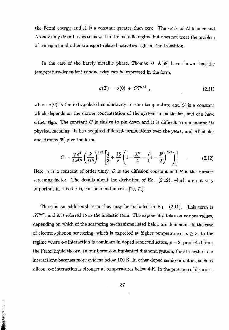
the Fermi energy, and A is a constant greater than zero. The work of Al'tshuler and
Aronov only describes systems well in the metallic regime but does not treat the problem
of transport and other transport-related activities right at the transition.
In the case of the barely metallic phase, Thomas et al.[68] have shown that the
temperature-dependent conductivity can be expressed in the form,
a(T) = a(O) + CT112 , {2.11)
where a(O) is the extrapolated conductivity to zero temperature and C is a constant
which depends on the carrier concentration of the system in particular, and can have
either sign. The constant Cis elusive to pin down and it is difficult to understand its
physical meaning. It has acquired different formulations over the years, and Al'tshuler
and Aronov[69) give the form
c = E (~)1
/2
[~ + 16 (1- 3F- (1- F)3/2)] 411"2/i Dn 3 F 4 2 {2.12)
Here, 'Y is a constant of order unity, D is the diffusion constant and F is the Hartree
screening factor. The details about the derivation of Eq. {2.12), which are not very
important in this thesis, can be found in refs. [70, 71 J.
There is an additional term that may be included in Eq. {2.11). This term is
STPI2, and it is referred to as the inelastic term. The exponent p takes on various values,
depending on which of the scattering mechanisms listed below are dominant. In the case
of electron-phonon scattering, which is expected at higher temperatures, p ~ 3. In the
regime where e-e interaction is dominant in doped semiconductors, p = 2, predicted from
the Fermi liquid theory. In our boron-ion implanted diamond system, the strength of e-e
interactions becomes more evident below 100 K. In other doped semiconductors, such as
silicon, e-e interaction is stronger at temperatures below 4 K. In the presence of disorder,
37

p = 3/2[72], while at the M-1 transition, p = 1[73].
We decided to ignore the term ZTPI2 since we could not measure conductivity of
our doped diamond specimens down into the milli-kelvin regime. Effects associated with
ZTPI2 are known to be important at temperatures below 1.5 K.
2. 7 The derivative method
The derivative method has proved to be a very sensitive tool for probing transport
properties in disordered systems[35]. Below I give a general overview of the derivative
method. Further reading on this theory can be found in Rosenbaum et al. papers[28, 29,
30] and references therein.
I have, for convenience, combined expressions for the electrical conductivity at low
temperatures into the form represented by Eq. (2.13):
CJ(T) =A (CJ(O) + crz exp [- (~) m] ) (2.13)
According to Hill[74] and Jonscher[75], and Zabrodskii and Zinov'eva(76], a compar
ison of the experimental data with Eq. (2.13) can be carried out in terms of the local
activation energy, W, defined as the gradient of an Arrhenius plot of the conductivity.
i.e.,
W 81nCJ _ T81nCJ =a1nr- or (2.14)
Substituting Eq. (2.13) into Eq. (2.14) gives,
38

z + m r;:r-m ~ m r;:r-m (strongly insulating)
W(T) = Z
zcrz 1 (a-(o) + crz) (weakly insulating)
(metallic)
(2.15)
From Eq. (2.15), we see that in the case of strongly insulating samples, W --+ oo as
T--+ 0. For weakly insulating materials, W = Z as T--+ 0, where Z is a positive finite
value. For convenience in handling the experimental data of strong insulating samples,
Eq. (2.15) is usually transformed into a straight line graph of the form,
logW = -mlogT +log(mT::") (2.16)
In the case of metallic samples, we have W(T) --+ 0 as T--+ 0, provided the term o-(0)
is non-zero. By allowing o-(0) = 0 (according to the scaling theory of localization[ll]),
we get W = Z. This means that W is independent of the temperature of the sample at
the transition. o-(0) can be obtained by writing the metallic equation (7.1) as
(2.17)
where constants Z and B, from Eq. (2.15), were obtained from a straight line graph of
the form
log (W(T) o-(T)) = ZlogT +log (Z C) (2.18)
The o-(0) values can therefore be extracted from the experimental data without having
to extrapolate the conductivity results to zero temperature.
39
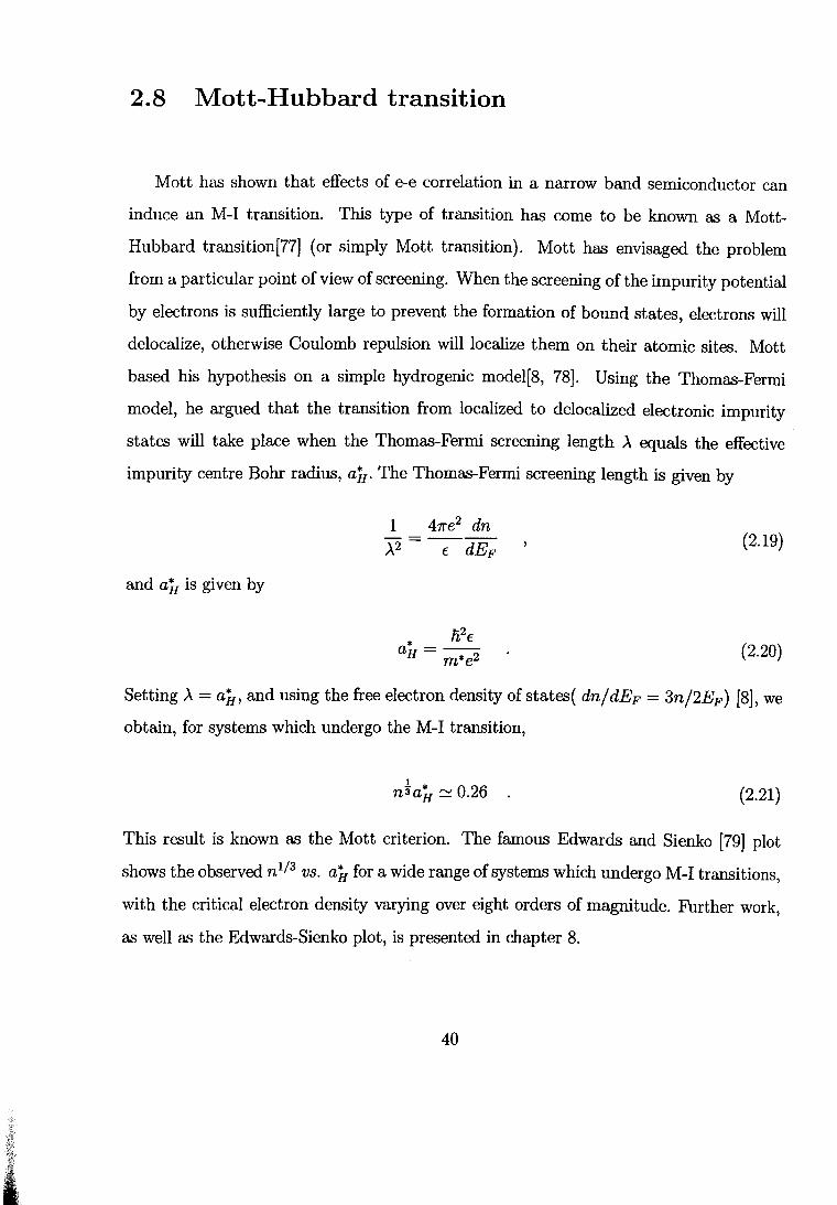
2.8 Matt-Hubbard transition
Mott has shown that effects of e-e correlation in a narrow band semiconductor can
induce an M-1 transition. This type of transition has come to be known as a Matt
Hubbard transition[77] (or simply Mott transition). Mott has envisaged the problem
from a particular point of view of screening. When the screening of the impurity potential
by electrons is sufficiently large to prevent the formation of bound states, electrons will
delocalize, otherwise Coulomb repulsion will localize them on their atomic sites. Mott
based his hypothesis on a simple hydrogenic model[8, 78]. Using the Thomas-Fermi
model, he argued that the transition from localized to delocalized electronic impurity
states will take place when the Thomas-Fermi screening length A equals the effective
impurity centre Bohr radius, a~. The Thomas-Fermi screening length is given by
1 4?re2 dn A2 = -t:-dEp (2.19)
and a~ is given by
(2.20)
Setting A= a~, and using the free electron density of states( dnjdEp = 3n/2Ep) [8], we
obtain, for systems which undergo the M-1 transition,
1 n3a~ ~ 0.26 (2.21)
This result is known as the Mott criterion. The famous Edwards and Sienko [79] plot
shows the observed n113 vs. a~ for a wide range of systems which undergo M-1 transitions,
with the critical electron density varying over eight orders of magnitude. Further work,
as well as the Edwards-Sienko plot, is presented in chapter 8.
40

A more rigorous picture on the study of the M-1 transition driven by e-e interactions
has been presented by Hubbard[77, 80]. Hubbard introduced a Hamiltonian for a system
of electrons that interact in a particular way. He considered a situation where two
electrons can interact only when they occupy the same site {intra-site interaction), and
ignored the long-range electron interactions (inter-site interactions). Using the tight
binding approximation, Hubbard suggested a Hamiltonian that can be expressed in the
form
{2.22)
where ct (ci' 8 ) are the creation {annihilation) operators which create {annihilate) an
electron of spin s { =i, !) on a site i, and nt = ctcis is an electron number operator
which counts the number of electrons of spin s on site i. The second term in Eq. {2.22)
is the on-site Coulomb repulsion between two electrons occupying the same site. On the
insulating side of the transition, an energy gap opens up in the DOS at the Fermi level.
This gap, of width (U-B), separates the lower band from the upper Hubbard band. In an
uncompensated semiconductor at zero temperature, the states in the lower band are all
filled with one electron per site and the upper band is empty. When the lattice constant
is reduced or the electron concentration is increased, the bands broaden and eventually
merge. An M-1 transition will occur when the bandwidth B for the non-interacting
electrons becomes equal to the intra-site repulsion energy U. A Mott-Hubbard transition
is shown in Fig. 2-3.
Both the Mott and the Hubbard treatments of the M-I transition completely ignore
the effects due to disorder and the magnetic behaviour of the system. In these models, a
regular array of donor sites is assumed. In real systems, there is always an element of dis
order which is evident in doped systems in which the dopants are randomly incorporated
into the system.
41
o- state o- bond
Is state 0 band
Figure 2-3: A schematic diagram showing the Mott-Hubbard transition brought about by electron-electron interactions. The model used by Mott and Hubbard ignores the effect due to disorder and the magnetic behaviour of the system. The splitting of the top band (D-1 band) into lower and upper Hubbard bands is due to Coulomb repulsion by intrasite electrons. At T = 0 K, the bottom band (D band) is completely filled with one electron per site, while the upper band is empty. The energy that separates the top band from the lower band is the difference between the Coulomb repulsion energy U and the bandwidth energy B, i.e., c2 = U- B. A metal-insulator transition will occur when U =B. This situation occurs when the inter~tomic spacing is systematically reduced to allow electron wavefunctions to overlap more strongly.
42

2.9 Scaling theory of localization
Early theoretical formulations of the scaling theory were presented by Thouless[81]
and Wegner[82]. Their work culminated in the 1979 paper of Abrahams et al.[11] which
has had great impact on this field and increased our understanding of the physics of M-I
transitions.
The scaling theory has made some interesting and very intriguing predictions. For
example, a thin long wire and a thin film are effectively 1- and 2- dimensional systems,
respectively, and their eigenstates are always localized in space irrespective of the amount
of disorder one introduces to these systems. These systems should be insulating at
sufficiently low temperatures. Many experiments have been carried out in trying to
observe these effects[83, 84].
In 3-dimensional systems, in which we are interested, the scaling theory predicts a
continuous M-I transition. The theory further suggests that the electrical properties of a
macroscopic system can be understood, based on information extracted from microscopic
properties of this system. We study this situation below.
Abrahams et al. [11] using the Kubo-Greenwood formulation, showed that the con
ductance of a system with a linear size L depends on perturbations to the boundary
conditions in the following way:
e2 t::..E(L) g(L) = 2/idE(L)jdN {2.23)
where dE/ dN is the mean spacing of the electron energy levels. The system for which
Abrahams et al. [11] derived this result is a hypercube of size Ld. (dis for dimensions.)
t::..E represents the geometric mean of the fluctuation in energy eigenvalues which is pro
duced when the boundary conditions are changed from periodic to antiperiodic on oppo-
43

site edges of a square. Thouless[81] had previously derived a dimensionless conductance
of the system as
e2
(W(L))-1
g(L) = 2/i B(L) (2.24)
where the ratio W ( L) / B ( L) may be taken as the localization criterion. The reader
may recall that, in the Anderson localization problem, W/ B was the main factor which
described the localization transition. Thus, a direct connection can be made between the
Anderson localization and the scaling theory. We now define the scaling function, in a
differential form, as
{3( (L)) = dlng(L) 9 dlnL (2.25)
where {3 depends only on g. Hence, this theory is referred to as a one-parameter scaling
theory. We consider situations in the asymptotic limits, g -+ oo and g -+ 0. In the limit
g-+ oo, the system obeys Ohm's law, whereg(L) is expressed as g(L) rv Ld-2• Taking the
limit on {3(g) gives lim {3(g -+ oo) rv d- 2. As g -+ 0, all states are exponentially localized,
and g(L) can be given as g(L) rv exp(-.XL). In this limit, {3(g(L)-+ 0) rv lng. Fig. 2-
4 shows the expected behaviour of {3(g(L)) as a function of lng. {3(g) = 0 defines the
critical conductance, g = 9c· This means tha:t any sample with the critical conductance
will have the same conductance for any value of length L. That is, g(nL) = g(L), where
n is a positive integer. For g < 9c, the conductance scales to zero at macroscopic length
scale, while, for g > 9c, the conductance scales to a large value[70]. 9c is a fixed point
which locates the mobility edge (i.e., energy separating the extended states from the
localized states) of the system. No minimum metallic conductivity is predicted by the
scaling theory. The minimum metallic conductivity is discussed later in the chapter. The
transformation of g ton (sample concentration) is valid as long as the relation between
the two is smooth and monotonic. The end result, in which we are interested, is given
by Eq. (2.28) in section 2.10.
44

2.10 Critical conductivity exponent
A great deal of experimental and theoretical work has been carried out over many
years to determine the critical conductivity exponent JL[16, 17, 18, 85, 86, 87, 88, 89,
90]. In spite of these years of intense effort, the critical behaviour of the electrical
conductivity a(O) in the vicinity of the M-I transition remains unresolved[91, 92]. Most
of the theoretical work done to date estimates JL to be unity[93, 94], while some theories
predict JL = 1/2[95, 96]. JL values close to unity have been found experimentally in
most amorphous M-I alloys, such as Ge:As[97] and Si:Nb[98], crystalline compensated
semiconductors such as Ge:Sb[99] and Si:(P,B)[19, 100], and in certain semiconductor
systems when measured in the presence of a magnetic field[87, 101]. Values of Jl close to
1/2 have been found in all uncompensated silicon-based semiconductors[88, 102, 103, 104]
and in some neutron-transmutation doped systems[65, 105].
The classification of disordered systems by their conductivity exponent Jl ~ 1/2 and
JL ~ 1 without a clear physical distinction constitutes what is known as an "exponent puz
zle". In other words, systems are assigned to universality classes based on their estimated
conductivity exponents, and not on the behaviour of a(O) in the critical regime. In our
case, we have determined JL ~ 1.7, which lies outside the two universal classes. It has been
suggested that systems which exhibit JL ~ 2 may have percolation characteristics[107J.
There is still an on-going debate on the methodology leading to the determination of JL.
Some of the main concerns are the following:
(i) the extrapolation to zero temperature of the measured temperature-dependent
conductivity,
45

l
~-ding -dlnl
d=3
Figure 2-4: Predictions of a one-parameter scaling theory of localization are depicted in this figure, where we have plotted the scaling function fl(g) as a function of In (g(L)). All states are localized in !-dimensional and 2-dimensional systems for any amount of disorder. 9c defines the critical conductance for a 3-dimensional system.
45

Figure 2-4: Predictions of a one-parameter scaling theory of localization are depicted in this figure, where we have plotted the scaling function j3(g) as a function of In (g(L)). All states are localized in 1-dimensional and 2-dimensional systems for any amount of disorder. 9c defines the critical conductance for a 3-dimensional system.
46

(ii) the determination of nc, in the doped systems,
(iii) the determination of the actual dopant concentration in these samples,
(iv) possible sample inhomogeneity, and
(v) the range of the experimental data used to determine nc.
The method presented below suggests ways of circumventing some of the problems
listed above.
2.11 Shlimak method
Near the M-1 transition, Maliepaard et al.[108] have shown theoretically that u(T) should
obey the form,
u(T) = u(O) + CT113 (2.26)
At the transition, u(O) is zero[67]. The applicability of the u(T) ex: CT113 law has been
demonstrated recently by Shlimak et al.[16] on two sets of Ge:As and Ge:Sb samples. A
new approach to analyze the conductivity measurements has been suggested in ref.[16],
in which p, and nc of the M-1 transition can be determined without extrapolating the
temperature-dependent electrical conductivity results to zero temperature. The principal
point of this method is to replace u(O) with l:l.u(T*) = un(T*)-unc(T*), calculated at any
temperature T* at which the conductivity obeys the general approximation, u(T) = a
+ CT P (p = 1/2 or p = 1/3). It follows therefore that
(u2(0) + CT*113)- (u(O) + CT*113 )
!::.u(T*) = u2(0)- u(O) (2.27)
u2(0) , since u(O) = 0 at the M-1 transition.
According to the scaling theory of localization[ll], u(O), when plotted against the impu-
47

rity concentration n, is equal to zero on the insulating side of the M-I transition, and is
finite for n > nc. In the vicinity of the M-I transition, a(O) is governed by the relation
(2.28)
We can also write Eq. (2.28), following Eq. (2.27), as
(2.29)
Eq. (2.29) can be transformed into a straight line form by taking logs on both sides to
give
(2.30)
where f-t is determined from the slope of a straight line graph using a least squares fitting
procedure.
In order to characterize the M-I transition, Shlimak et al. introduced a dimensionless
parameter, a, given by
>1
1
(metallic conductivity
(metal-insulator transition)
< 1 (insulating)
(2.31)
where temperatures R(TI) and R(T2) are resistances of a given sample measured at any
two temperatures in a regime where the power law, a(T) = a + CT113 , is observed.
Results obtained using the method of Shlimak et al. are reported in chapter 8.
48

2.12 Minimum metallic conductivity
IR[lO] have observed that no ordinary (macroscopic) metallic conduction will take
place when the electron mean free path l is shorter than the distance between the impurity
centres a. According to theIR criterion, there should be a lower limit in the Boltzmann
conductivity, and this limit is reached when l =a. At this point, the conductivity takes
the form:
e2 8 X 10-sn-l o-(O) = O"fR rv 31il = l . (2.32)
The idea of a lower conductivity limit was formalized into the concept of a minimum
metallic conductivity O"min by Mott in 1972 [109]. In a series of papers, Mott argued that
as the M-I transition was approached from above (metallic side), a(O) decreased with l
untill =a, and then the system became insulating, with an abrupt drop in a(O) from a
minimum value O"min to zero. O"min can be expressed in a general form:
e2 cl ( -4) 1 O"min =Cilia = -l- 2.4 X 10 n- (2.33)
where C1 is a numerical constant in the range 0.025 to 0.1. O"min is always smaller
than a1R due to the reduction in the density of states at the Fermi energy by electron
correlations[8]. Theoretical arguments, based on experimental results of Rosenbaum et
al.[27], have been presented by Mobius's group in support of amin[13]. Most experiments
on standard doped semiconductors, carried out by leading researchers in the field, have,
however, failed to observe O"min of the predicted magnitude but have measured conductiv
ities far below O"min[llO] and their results are consistent with the scaling theory, proposed
by Abrahams et al.[ll], which predicts a continuous M-I transition as T---+ 0 K.
For completeness and for reference purposes, I have added an outline of the weak
localization theory in this chapter.
49

2.13 Weak localization theory
The weak localization theory does not necessarily address the question of localization,
but computes corrections to the Boltzmann conductivity due to a special set of elastic
scattering events known as coherent backscattering. The term "weak localization" is
somewhat a misnomer and may be misleading. The theory obtains results from the weak
scattering regime, where the product of the Fermi wavevector and the elastic mean free
path is far greater than unity, i.e. kpl >> 1. Such a situation can only occur deep in the
metallic phase, far away from the transition in 3-dimensions. All states are computed to
be localized in a !-dimensional system and a 2-dimensional system. The theory acquired
its name from the latter context.
The basic ideas behind this theory were presented by Langer(lll) and Neal(112) in the
1960s, using Feynmann's diagrammatic techniques. Bergmann[113) has translated these
diagrammatic perturbation calculations into a very lucid physical picture. I present a
brief description of the central ideas of Bergmann below.
Consider an electron moving from point A to point B, as shown in Fig. 2-5. A
Feynmann diagram can be constructed with many possible scattering paths, depending
on the scattering that occurs, and each path has an associated amplitude. Ignoring
the interference effects due to multiple scattering, these accumulated amplitudes can be
summed and squared individually to give the total electron transmission probability from
A to B. Closed loops may occur, such as at point Z, shown in Fig. 2-5. In closed loops
only elastic collisions occur. In this case, phase coherence can be maintained around the
loop. This effect is called coherent backscattering. The loop provides two alternative
50

(complementary) paths, clockwise and anti clockwise, and these paths are time-reversal
pairs. Let the amplitudes of these transmission paths be 8 1 and 8 2 . Then the probability
of an electron to return to its starting position is given by
2
P = L 18;1 = !81!2 + !82!
2 + !8182! + !8281! (2.34) i=1
There are three possibilities from Eq. (2.34). When the paths are in phase at Z with
(2.35)
In the case of phase incoherence, !8182! = !8281! = 0, and we get
(2.36)
When the paths are out of phase at Z, 81 = -82 and 82 = -81, and we obtain
(2.37)
The higher the probability of an electron being in the closed loop, the less likely it will
conduct current leading to an overall reduction in conductivity. This effect is called weak
localization. This phenomenon can easily be destroyed by the application of a magnetic
field which destroys time reversal symmetry[113, 70], by an increase in temperature (in
elastic collisions are known to destroy weak localization at finite temperatures), etc.[114J.
If T 112 is the temperature dependence of the inelastic scattering process, then at high
temperature it will dominate the total scattering. A complete description of the theory
can be found in the review articles by Lee and Ramakrishnan [70] and Al'tshuler and
Aronov[115].
51
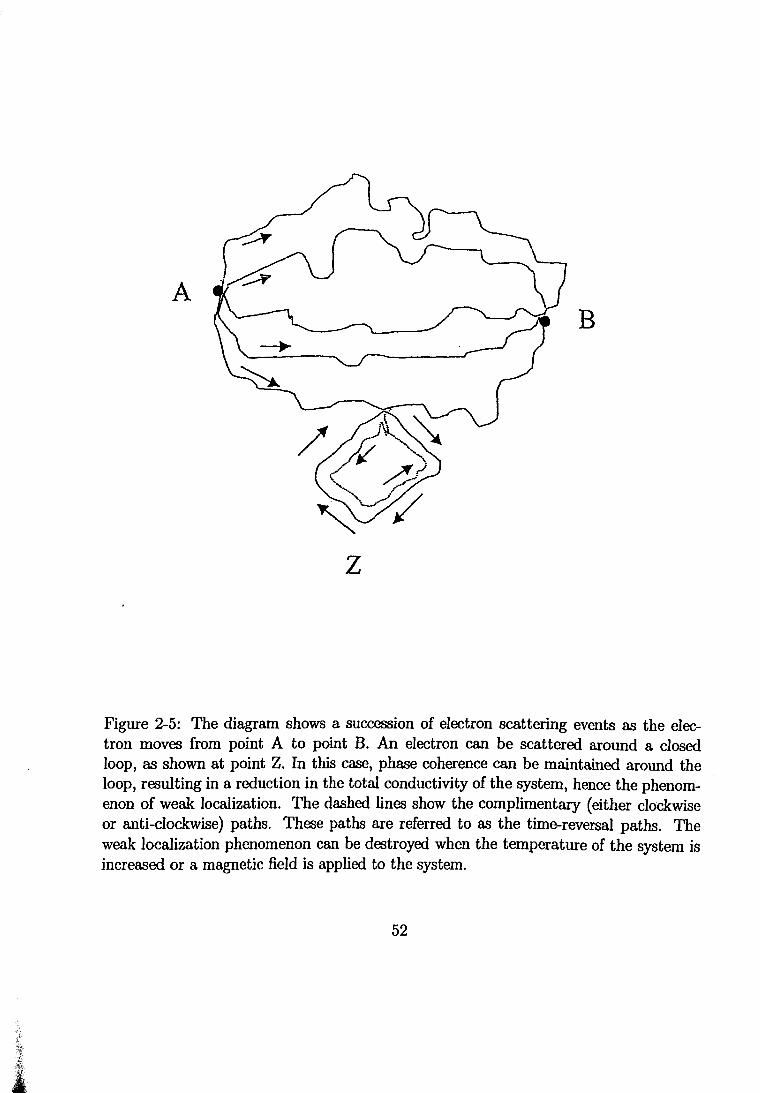
A B
z
Figure 2-5: The diagram shows a succession of electron scattering events as the electron moves from point A to point B. An electron can be scattered around a closed loop, as shown at point Z. In this case, phase coherence can be maintained around the loop, resulting in a reduction in the total conductivity of the system, hence the phenomenon of weak localization. The dashed lines show the complimentary (either clockwise or anti-clockwise) paths. These paths are referred to as the time-reversal paths. The weak localization phenomenon can be destroyed when the temperature of the system is increased or a magnetic field is applied to the system.
52

Chapter 3
Ion implantation
3.1 Introduction
Ion implantation is a process by which a flux of energetic atomic particles is introduced
by bombardment into the near surface region of any solid material. It is a process which
allows one to insert almost any impurity ion into any desirable target material regardless
of the phase diagram, solubility and thermodynamic metastability of the target. It is a
technique which permits the near surface properties, electrical, chemical and structural,
of any material to be modified as desired.
Since ion implantation is a high-energy process, with dopant atoms accelerated at
energies far exceeding the typical binding and displacement energies of atoms in the
target material, it is usually accompanied by severe radiation damage to the target.
It is the control or engineering of this radiation damage in producing well-characterized
implanted materials which is of interest in obtaining sample materials used in the present
experiments.
53

Doping of diamond by means of ion implantation has been attempted since the early
1960's but with limited success[116] until fairly recently [5]. The introduction and the
annealing of the resultant radiation damage, as well as the concomitant modifications
caused by these processes, is now fairly well understood, but, presently, only substitu
tional boron-ion doped layers can be selectively and reproducibly generated in single
crystal diamond surfaces. Some attempts at implanting other species into diamond
have been undertaken[117]. Progress in this field has recently been reviewed by sev
eral authors[5, 118].
In this chapter, the general processes which accompany the slowing down of ions as
they enter the target material are reviewed. The annealing and the possible graphitization
of the implanted surface layers during the high-temperature annealing are described. The
lattice expansion due to high ion implantation into diamond is briefly discussed. The
reaction-rate theory of point-defect interactions in diamond during the annealing stage
is outlined. I discuss the energy-loss simulation program Transport of Ions in Matter
(TRIM) applied to the implantation processes of interest, and the Secondary-Ion Mass
Spectroscopy (SIMS) profiles performed on boron-ion implanted diamond specimens.
3.2 General background
3.2.1 Stopping processes of ions in a solid
When an implanted ion enters into a substrate, it gradually transfers its kinetic energy
to the host atoms through two main scattering events: electronic and nuclear scatterings.
The first scattering mechanism, which is predominant at the beginning of the ion's path
through the substrate, is known as 'electronic stopping'. Here the kinetic energy of the
moving ion is lost through the excitation and ionization of the electrons of the substrate
54

atoms. It is, therefore, an inelastic scattering process. By this approach, the electrons in
a solid can be viewed as a free electron gas which is affected by a traversing positive ion
of the projectile. The inhomogeneity in the electron plasma introduced by the projectile
ion induces a retardation force on the ion, and hence a loss in the projectile energy.
AB the ion penetrates deeper into the substrate, it encounters more violent scattering
collisions with the host atoms, displacing some of them from their lattice sites. Towards
the end of the ion range in the substrate, the remainder of the kinetic energy is lost
through ballistic displacement collisions with atoms. This is the nuclear stopping process.
Despite having the same incident energy when entering the substrate, ions have differ
ent random impact parameters with the surface atoms. This results in a different number
of collisions and path lengths for each ion before coming to rest. Since the slowing down
of ions is a statistical process, the ion distribution in the host should be expressed using
statistical variables. The distribution of the implants in the host can be approximated by
a (symmetric) Gaussian curve[119]. The density of the implanted species as a function
of the distance x (measured along the beam direction) is given by
(3.1)
where np is the peak ion density at Rp. The parameter, Rp, is the projectile range which
gives the mean penetration depth of the ion relative to the surface, while ~Rp is the
standard deviation in the projectile range (also referred to as the ion range straggling).
This Gaussian approximation paints a simple physical picture of the implant profile.
It ignores the substrate temperature, which is particularly important when interstitial
diffusion and higher order effects occur. The theoretical details can be found in an article
by Prins[119].
When the imparted kinetic energy from the incident ion to the substrate is greater
55

than the displacement energy, a Frenkel defect (a closely separated vacancy and intersti
tial) is formed. The displacement energy of diamond has been estimated by a number
of authors. Prins[120] has used a value of 55 eV in his work, but the present consensus
favours a value of ~ 35 eV[121]. If the interstitial and the vacancy that are created
do not recombine spontaneously, and the interstitial still possesses some kinetic energy
greater than the displacement energy after collision, it will move away from the vacancy
and continue to collide with stationary target atoms, whereupon more Frenkel pairs may
be created. In addition to this process, the recoiling interstitial may transfer its kinetic
energy along a close-packed row of atoms in a sequence of replacement collisions. The
resultant interstitial from this replacement collision will be located far away from the
original vacancy, preventing any interstitial-vacancy (Frenkel pair) recombination. Also,
secondary cascade collisions occur when the substrate atoms absorb energies far greater
than the displacement energy, and thus in turn continue to knock off other atoms from
their lattice positions, creating more vacancies and interstitials.
When the implanted ion reaches its final range in the host, it dissipates all its remain
ing energy to the surrounding substrate atoms. This results in an isolated (localized)
region of high vacancy density (depleted zone). As the fl.uence is further increased, these
damaged isolated regions may overlap and coalesce to form new vacancy-related phases.
Unless controlled, the agglomeration of the vacancy defects could lower the material
density, and eventually produce surface graphitization.
The reason why more vacancies are created when the ion reaches its final projectile
energy range has to do with elastic momentum transfer of the incident ion to the substrate
atoms. As the momentum of the implanted ion continues to decrease, its cross section
for elastic scattering off the host atoms increases. The slower the ion traversing thorough
the substrate, the longer is the period of time over which momentum transfer to another
ion occurs. Slower ions are more capable of displacing the substrate atoms from their
56

lattice positions by ballistic collisions than faster moving ions, which require a more direct
"head on" collision to effect the same displacement. When the energy of the incident ion
drops below the displacement energy, no more vacancies are created. The ion eventually
comes to rest in a depletion zone, either in an interstitial or substitutional site. The
model described above is captured in Fig. 3-1. It does not, however, present a stable
picture. It is only applicable at temperatures below which the points defects are immobile.
When the substrate temperature is high enough for interstitials to diffuse, more Frenkel
pairs are annihilated thus reducing the lattice damage. At these elevated temperatures,
some of the interstitials can escape from the damaged layer, while the residual vacancies
remaining behind may agglomerate into more complex defect structures[l22].
Owing to the fact that diamond is a metastable form of carbon, there exists a crit
ical threshold determining how much damage an implanted layer can suffer before an
irreversible structural change (graphitization) occurs. The critical dose at which graphi
tization can be initiated depends on a number of factors, most of which are discussed in
a fairly recent book by Dresselhaus and Kalish[5]. Some of these factors are:
• The target ions used for implantation - massive ions generally lead to more damage
than lighter ones owing to their larger stopping powers.
• The dose rate (beam current) - slow implantation is characterized by a slow arrival
rate of ions at the target surface, and this may allow the system to partially recover
from the radiation damage before further implantation-induced damage is produced
in the same volume in the target. Fast implantation may cause overlap of the
damage cascades, resulting in a different kind of damage profile. The implantation
rate is expressed in terms of the beam current density in units of J-LA/cm2• Values
in the range of 1-1.6 J-LA/cm2 , corresponding to slow implantation, were used in our
case. Typical values for fast implantation are in the range of 100 J-LA/cm2 or more.
57

Exchange Dynamic
Energy transport~-byfocusons
Figure 3-:-1: A simplified schematic description of the damage cascade introduced during the ion-implantation process. This figure is taken out of ref.[5].
58

• Orientation of the target material to the beam of implanted ions - different levels
of radiation damage are generated when a target is oriented in a random direction
than when the implanted ions channel through the substrate materials.
• Ion dose - whether ions are implanted into a target material in a single step or
distributed in multiple steps.
• Implantation temperature - different types of damage are created when the tar
get temperature is varied. Increasing the implantation temperature substantially
increases the mobility rate of both the implants and the created defects, and thus
increases the probability of interstitial-vacancy recombinations. The damage pro
file will spread out when the substrate is implanted at elevated temperatures, while
implantation at a low temperature is desirable for maintaining a sharp impurity
distribution profile.
• Type of annealing used - the type of point defects that are formed and their density
depend on the annealing cycle employed. The duration of anneal does not appear
to alter the electronic properties of the diamond specimens in a very significant
way.
The last two factors, i.e. the implantation temperature and the annealing cycles used,
are important in this thesis and are further described below. Chapter 6 is devoted to the
results obtained using various annealing routines employed in this work. The first four
factors mentioned above are described in the experimental chapter (chapter 4).
59
3.3 Implantation temperature
3.3.1 Cold-implantation followed by rapid-temperature anneal
ing cycle
The most successful scheme for reliable doping of diamond samples involves cold implan
tation followed by rapid thermal annealing. The basic idea behind the CIRA technique is
that the diamond substrate is implanted while held at liquid nitrogen temperature to im
pede the diffusion of the point defects, followed by rapid annealing to high-temperatures
to allow the diffusion of both vacancies and interstitials. This encourages interstitial
vacancy recombination and dopant atom-vacancy combination in the damaged layer,
thus minimizing the radiation damage[123, 124].
I wish to make the reader aware of some inherent complications associated with
the CIRA routine. I have broken these 'complications' into small sub-topics below to
highlight their importance or influence on the CIRA scheme.
3.3.2 Selection of the ion energies and doses
The ion-implantation energies and the doses that one selects to implant into the diamond
substrate should be kept low enough so as not to exceed the amorphization threshold. As
mentioned in section 3.2, ion-implantation by more massive ions than the target atoms
can give rise to huge radiation damage and this may lead to immediate amorphization
(or graphitization) of the implanted layer during annealing. Less massive ions or ions
with masses close to that of the target atoms yield reproducible results provided certain
procedures are used[125]. The implantation energies and the doses must be spread evenly
to intermix the point-defects and to ensure their proximity within the ion-implantation
60

damaged layer. This is to increase the probability of the point-defects interacting with
each other during the annealing stage. Failure to follow a multi-step small dose implan
tation sequence can lead to results not being reproducible.
3.3.3 Activation of dopant-interstitials
Studies reveal that some boron interstitials, which do not become activated, diffuse out
of the implanted layer during the high-temperature annealing, leaving behind an ex
cess of vacancies[118]. A large concentration of vacancy-defects are known to lower the
material density and this can lead to the amorphization or graphitization of implanted
surface layers in diamond. In order to avoid this process from taking place, one needs
to optimize the implantation-annealing parameters. The manipulation, or choice, of the
implantation-annealing parameters leading to the distribution of the dopant atoms in the
surface layer are crucial in this study, and have been examined.
3.3.4 Behaviour of self-interstitials in the damaged layers
Carbon self-interstitials and boron-interstitials do not behave in the same manner during
the annealing processes. Recent studies show that self-interstitial-vacancy recombinations
increase with increasing annealing temperature, while boron-interstitial-vacancy combi
nations decrease as most of the boron diffuse away from the implanted layer[126, 127].
This behaviour of can be modelled in terms of two activation energies for each inter
stitial type: an energy for activation (interstitial-vacancy recombination) and an energy
for self-interstitial diffusion[120]. A two-stage high-temperature annealing process, fol
lowing the cold-implantation, has been the route to follow in an effort to encourage
boron-interstitial-vacancy combinations.
61

3.3.5 Behaviour of vacancies in ion-implanted layers
Vacancies prefer to interact with each other to form more complex structures rather than
to combine with other point-defects[118]. The presence of these complex defect structures
in the damage cascade is a serious drawback in our efforts to effectively remove the
radiation damage introduced during ion-implantation. Moreover, these complex-vacancy
defect structures are known to be optically and electronically active, and act as deep
lying donors which can compensate the activated boron acceptors. They have been found
to lie about 4 eV below the conduction band[6, 7].
3.3.6 High-temperature implantation
This section has been included for completeness as no attempt has been made to implant
our diamond specimens at elevated temperatures. All our implants have been carried
out at liquid nitrogen temperature.
To avoid any permanent damage (apart from the formation of extended defects which
are very difficult to remove) such as surface graphitization and to greatly reduce the
levels of radiation damage in the implanted layer, most workers have chosen to implant
their diamond specimens at temperatures above 570 K[128, 129, 130]. Such an approach
has been based on the knowledge that the closely separated carbon self-interstitials and
vacancies which occur in the implantation process induce damage cascades, but will
readily recombine if given sufficient thermal excitation. This reduces the need to carry
out post-implantation annealing. If dopant interstitials are introduced in a vacancy rich
region during the high-temperature implantation, their activation probability will be
enhanced accordingly. It should be pointed out that such an approach has some short
comings, as was later discovered in a depth-profiling study on the distribution of the
carbon ions in diamond by Spitz et al.[131]. This study has revealed that the implanted
ions are, on average, located deeper than the vacancies in the damaged surface layer. It
62

follows, therefore, that by the time the implanted ions have diffused into the vacancy-rich
regime, the majority of the vacancies would have been annihilated by the carbon self
interstitials, leaving only a few vacancies for dopant activation. Another disadvantage of
the high-temperature annealing procedure is that the presence of these extended defect
phases degrades the electrical performance of the doped layer[132].
3.4 Annealing studies
3.4.1 Motivation
The two main purposes of annealing are to reduce the levels of radiation damage inflicted
on the diamond surface during the implantation process, and to drive the implants into
the desirable lattice sites (usually substitutional sites), where they act as donors or ac
ceptors. Both these processes can be realized when sufficient energy is imparted to the
point defects in the damaged region.
Annealing can be classified into two categories: high-temperature anneal and low
temperature anneal. I briefly describe these annealing procedures below.
3.4.2 High-temperature anneal (T > 770 K)
Above 700 K, both the interstitials and vacancies diffuse in the damaged diamond layer.
This increases the probability of interstitial-vacancy recombination. Those point defects
that do not recombine with each other either diffuse away from the damaged layer or
agglomerate to plate out as dislocations and other complex, extended defect phases.
Recent studies indicate that the major fraction of the vacancies agglomerate rather than
63
diffuse out of the implanted layer[118). These vacancy-related defects have been found
to act as deep lying donors and are situated about 4 eV below the conduction band[133).
When annealing vacancies in the implanted layer over the temperature range of 870
to rv 2000 K, compensating donors with large degeneracy weighting factors gn form.
It is postulated that these vacancies are formed by single vacancies diffusing towards
each other and in the process generating regions in which their wavefunctions overlap
into extended structures[133). They occupy positions separated by fewer carbon atoms.
These proposed 'vacancy-crystallites', it is argued, have the electronic properties of a
single vacancy, but with an apparently large degeneracy factor[120). In a boron-doped
layer, the vacancy defects will partially compensate some of the boron acceptors[134).
3.4.3 Low-temperature anneal (T < 770 K)
Only the interstitials can diffuse in this temperature region while the vacancies are still
immobile. Some fraction of the interstitials will annihilate with stationary vacancies,
while others will diffuse out of the damaged layer without recombining with vacancies,
leaving behind an excess of vacancies. The latter region, which is manifested by the
volume expansion of the damaged layer, has been measured by Maby et al. (135) and
Prins et al.[136] in boron-ion doped diamond specimens that were implanted at different
temperatures. Maby et al.[135] implanted their samples at room temperature, while
Prins et al. [136) used the CIRA process. The concept of volume expansion is discussed
in the next section.
3.5 Lattice swelling
I wish to discuss another phenomenon which may not be related to simple graphitiza-
64

tion of the implanted layers in diamond as discussed above. This phenomenon is known
as the lattice swelling, i.e. volume expansion as a result of high ion-dose implantation
into diamond. The expansion is reflected in the swelling of the implanted region when
the difference between the implanted region and the non-implanted region is taken (no
ticeable as step heights). This swelling has been found to depend on the implantation
temperature.
Three factors may be attributed to increases in lattice volume as a result of ion-implantation.
These factors are
• the addition of extra atoms, introduced into the lattice by ion implantation,
• the creation of point-defect (interstitials and vacancies) in the collision cascade
during implantation, and
• the possible thermodynamic phase transformation from compact diamond into a
graphite structure which is less dense than diamond.
Lattice expansion has been observed by various authors in diamond, but different
interpretations for its onset have been given. Early observation of the lattice swelling
was presented by Maby et al.[l35] after implanting a diamond specimen with 200 keV
B-ions at room temperature. They explained the swelling of the implanted region as due
to the creation of an amorphous region, which has graphite density. Maby et al. (135]
established a critical boron-ion threshold of 5 x 1015 cm-2 beyond which the onset of
irreversible volume expansion occurs. Below this critical threshold, they did not find any
measurable volume expansion.
A different approach to the processes that determine the electrical and structural
properties of diamond subject to ion implantation has been given by Prins et al.[l36,
65

137]. According to Prins et al. [136, 137], volume expansion and the high electrical
conductivity observed in ion-implanted diamond specimens are due to the difference in
the spatial distribution of the point-defects (interstitials and vacancies) created in the
damage cascade and the difference in their diffusivities. Since self-interstitials are mobile
at T rv 330 K and vacancies start to diffuse at T "' 750 K, Prins et al. [136, 137] have
observed that a higher degree of lattice swelling will occur in samples which have been
implanted at elevated temperatures than at low temperatures (T < 330 K). The escape of
some self-interstitials from the damaged layer at high-temperatures (330 K< T < 750 K),
with vacancies still locked in, should exhibit volume expansion. They demonstrated the
lattice swelling by implanting a diamond specimen with 170 ke V fluorine ions at T rv 100
oc, and found that the lattice expansion increased linearly with a fluorine dose up to
4 x 1016 cm-2. Contrary to claims made by Maby et al.[135] on graphite density-induced
swelling, Prins et al. [136, 137] have presented arguments as to why graphitization is an
unlikely process to explain the swelling in heavily implanted diamond.
3.6 Energy-loss simulation program: TRIM92
The most commonly used energy loss simulation code for ion-solid interactions is the
TRIM program. It was developed by Ziegler et al. [138]. The TRIM program incorpo
rates the best known semi-empirical values as well as the statistical nature of interaction
of the point-defects in the damaged layer. The program calculates the kinematics of
incident ions individually as soon as they collide with the substrate atoms. It then fol
lows the trajectory of recoiling target atoms which undergo further collisions that may
initiate new target atoms in motion, thus creating a branch of recoiling target atoms.
The program returns and continues to follow the motion of the original implanted ion
once all the recoiling atoms have attained energies below a certain cutoff energy. The
program repeats the above procedure until the primary ion comes to rest or is no longer
66
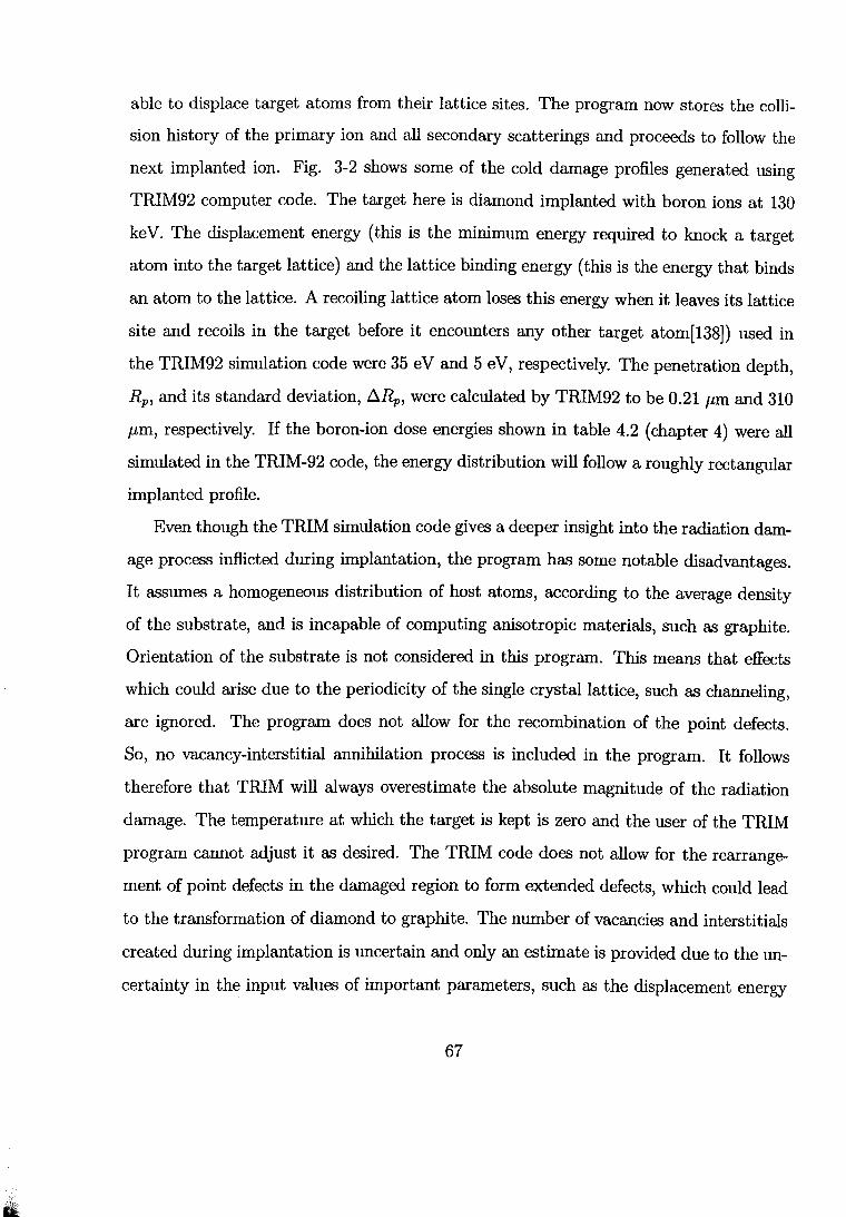
able to displace target atoms from their lattice sites. The program now stores the colli
sion history of the primary ion and all secondary scatterings and proceeds to follow the
next implanted ion. Fig. 3-2 shows some of the cold damage profiles generated using
TRIM92 computer code. The target here is diamond implanted with boron ions at 130
keV. The displacement energy (this is the minimum energy required to knock a target
atom into the target lattice) and the lattice binding energy (this is the energy that binds
an atom to the lattice. A recoiling lattice atom loses this energy when it leaves its lattice
site and recoils in the target before it encounters any other target atom[138]) used in
the TRIM92 simulation code were 35 eV and 5 eV, respectively. The penetration depth,
Rp, and its standard deviation, !1RP, were calculated by TRIM92 to be 0.21 pm and 310
pm, respectively. If the boron-ion dose energies shown in table 4.2 (chapter 4) were all
simulated in the TRIM-92 code, the energy distribution will follow a roughly rectangular
implanted profile.
Even though the TRIM simulation code gives a deeper insight into the radiation dam
age process inflicted during implantation, the program has some notable disadvantages.
It assumes a homogeneous distribution of host atoms, according to the average density
of the substrate, and is incapable of computing anisotropic materials, such as graphite.
Orientation of the substrate is not considered in this program. This means that effects
which could arise due to the periodicity of the single crystal lattice, such as channeling,
are ignored. The program does not allow for the recombination of the point defects.
So, no vacancy-interstitial annihilation process is included in the program. It follows
therefore that TRIM will always overestimate the absolute magnitude of the radiation
damage. The temperature at which the target is kept is zero and the user of the TRIM
program cannot adjust it as desired. The TRIM code does not allow for the rearrange
ment of point defects in the damaged region to form extended defects, which could lead
to the transformation of diamond to graphite. The number of vacancies and interstitials
created during implantation is uncertain and only an estimate is provided due to the un
certainty in the input values of important parameters, such as the displacement energy
67

z 0 i= <( a: .... z w () z 0 ()
0
IMPLANTED I BORON ATOMS~
2.o.Rp
100 200 Rp 300
DEPTH BELOW SURFACE (nm)
Figure 3-2: A typical figure showing a cold-implantation damage profile of a diamond specimen implanted with boron-ions which were accelerated into the diamond surface at 130 keV. This profile was obtained using the TRIM-92 computer simulation program in which the following parameters were supplied to the program: the displacement energy, Ed= 35 eV, and the binding energy, Eb = 5 eV. The penetration depth (projected ion range) is given by Rp, while straggling (i.e. the standard mean deviation from Rp) is denoted by 6.Rp.
68

and ionization energy.
3. 7 Secondary ion mass spectroscopy (SIMS)
SIMS is an ion beam probing technique in which target atoms are selectively removed
from the surface by sputtering. Sputtering is achieved by using low-energy (1-10 keV)
heavy ions, and the sputtered particles are analyzed in extremely sensitive high resolution
mass spectrometers. The typical resolution of ~M/M is of the order of 1:10 000, and the
method can resolve isotopes and other species ejected from the target material. In the
case of our diamond specimens, the SIMS analyses were performed using a CAMECA
IMS-4f double focusing, magnetic sector ion microanalyzer. The primary ion beam and
the beam energy used were o; and 8.0 keV, respectively. To avoid surface heating, the
beam current was adjusted to 0.16 and 0.312 f.J-A.
The SIMS analyses on our two diamond specimens were carried out by Charles Evans
and Associates in the United States. The actual doses implanted in these samples were
1.2 x 1016 cm-2 and 7.9 x 1016 cm-2. SIMS measured these doses to be 1.2 x 1016 cm-2
and 7.3 x 1016 cm-2, respectively. The thickness of the implanted conducting surface
boron-ion layers was estimated to be 0.25 Jl-m. Fig. 3-3 and Fig. 3-4 show plots of SIMS
depth profiles for these two diamond specimens. There are some obvious disadvantages
associated with the SIMS technique. It is destructive to the very surface layers it is
intended to probe. In the case of diamond, heavy-ion sputtering could lead to surface
graphitization, thus causing very basic alterations to the diamond specimen during the
process of analysis. SIMS is incapable of resolving the crystallographic location of the
desired ions, i.e. whether they occupy interstitial or substitutional lattice sites. This
means it is insensitive to the crystallinity of the specimen under investigation.
69

w22.---------------------1o7
Square Piece
,-.. ..,a to• en
~ 0
~
'-0
8 !019 0
0 s:: 0
1d I
H
~ --Gold Coat 103 ~ ...._, ~ ~
'0 0
s:: .... ~
0 ()
1-t i019 «<
-a (JJ
0 0 taZ ~ 0 0
1017 101
Depth (pm)
Figure 3-3: SIMS profile for a square boron-ion implanted type Ila diamond specimen. The actual total dose implanted into this sample was 1.2 X 10
16 cm-
2• SIMS measured
the same dose as implanted. The sample was annealed at 1200 oc for 30 minutes after
each implantation process.
70

1QEr---------------------~----------
Rectangular Piece
C-> 105
1020 ..........,.
\ a 0
............ a to• en -a
0
~ ::I 0
I 1019
0 ~ ~
~ 0
~ 0
~
..... 103 >a 1d --Gold Coat ~ ,.. "'d
~ ~ G)
0 0
0 G)
~ !0~8 0 {/]
0 102
Depth (J.UU)
Figure 3-4: SIMS profile for a rectangular boron-ion implanted type Ila diamond specimen. The actual dose implanted into this sample was 7.9 xl016 cm-2 using multiple CIRA steps. The SIMS measured the boron atoms in the implanted layer to be 7.3 x 10
16
cm-2• This sample was annealed at 1200 oc for 5 minutes after each implantation process.
71

Chapter 4
Experimental details
4.1 Introduction
Sample preparation, procedures, experimental techniques and apparatus used in the
study are described in this chapter. The first section focuses on the electrical conductivity
measurements carried out between 1.5 :::; T :::; 300 K, while the second section focuses
on transport measurements performed in the range of temperature 300 < T :::; 773 K.
We have used a Janis cryostat and a "dip" measuring system to carry out the electrical
conductivity measurements in the temperature range 1.5 - 300 K.
4.1.1 Sample designation
Fig. 4-1 shows one of the type Ila diamond specimens used in this study. The samples
have distinctive features by which we can recognize them, as is evident in Fig 4-1. Sample
A, which is the main sample, has a dot near the centre. Sample B has two rings at the
middle, while sample C has a clear, unmarked surface. Sample D was shaped into a
72

square after it broke off from a rectangular piece while we were trying to mount contacts
under pressure.
Alphabet symbols A to D denote samples. The next letter indicates the implanted
ion species. In this case, B stands for boron ions. A number following the alphabet
symbol represents a dose fiuence implanted into that sample.
4.1.2 Diamond shaping and polishing
Two of our type Ila diamond specimens were sawn off from one parent stone, while
the other two were cut from different stones. Three of the diamonds were shaped into
rectangular slabs of dimensions 8 x 3.5 x 2 mm3 using a diamond saw covered with a
diamond powder and oil. One sample, which broke off from one of the rectangular pieces,
was transformed into a square shape of dimensions 4.74 x 3.6 x 3 mm3 . Samples were
then polished on a cast iron polishing wheel of about 60 em in diameter, called a scaife.
To avoid channeling during ion implantation, samples were oriented 12° off the (110)
direction. Information on the preparation of diamond specimens is now commonplace,
and the reader is referred to chapter 8 of a fairly recent book on Ion Implantation in
Diamond, Graphite and Related Materials by Dresselhaus and Kalish[5].
4.1.3 Diamond target holder
Special masks, made out of a graphite disc and supported on a stainless steel backing
plate, were used to clamp diamonds to the target mounts. Stacks of mica rings were used
to provide circumferential support surrounding the diamonds inside the target mounts.
Mica, a material which is easily machinable, was sliced into discs of uniform thicknesses.
Implantations were carried out through graphite masks defining rectangular areas of 7 x 3
mm2 on the highly polished diamond surfaces. A new design was recently put into use,
73

Figure 4-1: Shown in this figure is sample A which is one of the four type Ila diamond specimens used in this thesis. The dimensions of tllis sample can be read off from the figure.
74

which allowed us to clamp samples by the sides directly to the target holder without
the use of graphite disc masks. Using the new set up, a whole diamond surface can be
implanted. Previously, we could only mount one sample per side on the target holder.
The new design allows us to mount all four samples on one face of the target holder,
provided the same dose is to be administered into all the samples.
A target holder was made up of a stainless steel block supported by a hollow tube.
The latter was used as a liquid nitrogen reservoir, since we carried out all our implants
at liquid nitrogen temperature. A stainless steel holder was used due to its poor thermal
conductivity, since the samples had to be transferred from the implanter's end station,
after the implantation process, into a liquid nitrogen bath.
4.2 Ion implantation
Ion implantations were performed using the Varian Extrion Model 200-20A2F ion
implanter stationed at the Schonland Research Centre. The end station of this implanter
has been specially modified to allow one to use a variety of target holders. The substrate
temperature was monitored with the aid of a chromel-alumel thermocouple which was
mounted at the back of the sample holder. In order to avoid condensation on the diamond
surfaces, liquid nitrogen was only poured into the reservoir once a vacuum of about
3 x w-6 torr was established at the end station. After the implantation process was
completed, the end station was vented with a dry nitrogen gas before dismounting the
target holder and transferring it, as quickly as possible, into a styrofoam bath filled with
liquid nitrogen.
While samples were still immersed under liquid nitrogen, the annealing furnace was
75

preset to a desired temperature, and allowed to stabilize for about 30 minutes. The
diamond was then dismounted from the target holder whilst under liquid nitrogen, and
transferred into a liquid nitrogen-containing styrofoam cup that was cut to size, with
a small groove made to accommodate and lock the diamond sample in a stationary
position. The sample was then slid down, with no time delay, into a high-temperature
preset annealing crucible.
4.3 Annealing furnace
The annealing furnace used for this study is shown in Fig. 4-2. It consists of a
quartz glass tube with a chimney[6, 7, 139]. Inside the quartz tube is a graphite crucible
which is heated by a water-cooled rf (radio frequency) coil. Rapid annealing is achieved
by allowing the diamond to slide, implanted face down, along the inclined quartz tube,
guided by a retractable quartz chute, into a preheated graphite crucible. Temperatures
ranging from 773 K to 2000 K were used in annealing the implanted diamond speci
mens. The temperature settings in the annealing furnace were achieved by the use of a
tungsten/rhenium thermocouple. Throughout the anneals, the furnace was flushed out
continuously with inert ultra-pure argon gas to inhibit graphitization on the implanted
diamond surface. As a precaution after each anneal, the diamond sample was left in the
furnace to cool down to close to room temperature before dismounting from the anneal
ing device. The sample was then placed on top of a metal substrate and allowed to cool
down to room temperature before cleaning.
4.3.1 Cleaning of diamond samples and sample storage
Samples were cleaned by boiling them in an acidic solution of sulphuric, nitric and per
chloric acids mixed in the ratio 3:4:1. They were boiled in a small beaker covered by a
76

ARGON OUT----
DIAMOND SLIDING DOWN CHUTE
---RF-COIL
~~-GRAPHITE
CRUCIBLE M-r1'----CERAMIC SEAT
#-------QUARTZ TUBE
Figure 4-2: A diagram of the annealing furnace used to anneal our diamond specimens after the cold ion-implantation process. Samples were slid down the retractable chute with the implanted face down into a preheated graphite crucible. The annealing was carried out in a pure-argon atmosphere.
77

watch glass until the acidic solution developed a dark yellow colour, and were allowed
to simmer in this solution for about 60 minutes to dissolve graphite and amorphous car
bon on their surfaces while leaving diamond specimens intact. Boiling of samples for
more than 60 minutes is sometimes necessary, particularly after we have carried out a
2000 K anneal. Afterwards, samples were rinsed thoroughly in distilled water and dried.
Cleaning of samples was performed pre and post implantation-annealing cycles.
After cleaning, samples were wrapped with a tissue paper, sealed in a transparent
plastic case, and stored at room temperature until needed for further measurements.
4.3.2 Implanted boron and carbon ions dose levels
Boron ions were implanted into the diamond targets at different energies in order to create
a highly conductive boron-ion surface layer in which the dopant ions and the other point
defects would be fairly evenly distributed. For the most reliable and reproducible results,
small implantation steps have to be followed using the CIRA method. Table 4.1 shows
the accelerating energies, boron-ion and carbon-ion dose fluences administered into the
diamond samples. The same boron-ion dose level has been used throughout to build-up
a highly conductive layer into the diamond samples. Because of the rapid change in
electrical conductivity with carbon-ion dose, the ion dose range which has been used is
rather narrow. Samples with the total carbon-ion dose that lie in the interval, 5.60 x
1015 cm-2 to 5.95 x 1015 cm-2, were prepared. The only difference in the procedure
followed in preparing our samples was that the carbon-ion doped samples were repolished
after each CIRA and electrical conductivity measurements.
Ohmic contacts were achieved by evaporating gold strips at the ends of the diamond
specimens. A standard spacing of 5.5 mm between the gold strips was kept in the case
78

Ion Energy {ke V) Dose (cm-2 ) x 1014 Dose (cm-2) x 1Q14
B 130 11.25 18.75
110 3.75 6.25
90 1.875 3.125
80 1.875 3.125
70 1.875 3.125
60 1.875 3.125
50 1.875 3.125
40 1.875 3.125
30 1.875 3.125
Total B-ion dose -+ 3.0 x 1015 cm-2 5.0 x 1015 cm-2
Ion Energy (Ke V) Dose (cm-2) x 1015 Dose (cm-2) x 1015 Dose (em - 2) x 1015
c 150 2.24 2.30 2.38
120 1.456 1.495 1.547
80 1.232 1.265 1.309
50 0.672 0.690 0.714
Total C-ion dose -+ 5.60 x 10¹⁵(cm-2) 5.75 x 10¹⁵(cm-2) 5.95 x 10¹⁵(cm-2)
Table 4.1: Implantation energies and ion doses used in this study. The accelerating energies and doses were spread into small steps to generate highly conducting boron-ion and carbon-ion layers in the diamond samples.
79

of three samples (A, B and C), and a spacing of 1.5 mm was left as a measurable region
for sample D. Evaporation of gold onto the samples were carried out at the Electron
Microscope Unit, and a thickness of about 100 nm was deposited. Fig. 4-3 shows plots
of I (A) vs. V (V) to demonstrate ohmic behaviour exhibited by sample A for a variety
of doses implanted onto the surface.
An alternative way of achieving good ohmic contacts was by means of heavy ion
implantation. In this case, we covered the regions where the electrical conductivity
measurements were to be made with an aluminium foil or a copper slab and only exposed
those regions on which we wanted to create contacts. As described above, a spacing of
5.5 mm was covered with a foil prior to contact implantation. A total dose of 6.1 x 10¹⁵
B-cm-2 was then implanted, broken up into small steps at different energies. Table 4.2
summarizes the ion dose and various energies used to generate these contact regions.
Linear ohmic contacts were achieved by applying silver paint onto the contact regions
and then baking the diamonds in an oven at 70-80 oc for over 2 hours[118). Table 4.3
gives a summary of sample characterizations. The rectangular diamond samples used in
this study have dimensions 8 x 3.5 x 2 mm3. The thickness, t, of the implanted layer
has been estimated by the SIMS technique to be 2200 . The square resistances in table
4.3 were obtained using the procedure: Ro = t (W / L) ~ , where W is the width of
the sample, L is the distance between the electrical contacts and R(n) is the sample
resistance at any measured temperature. a= 1/ Ro in units of (n- cm)-1 .
80
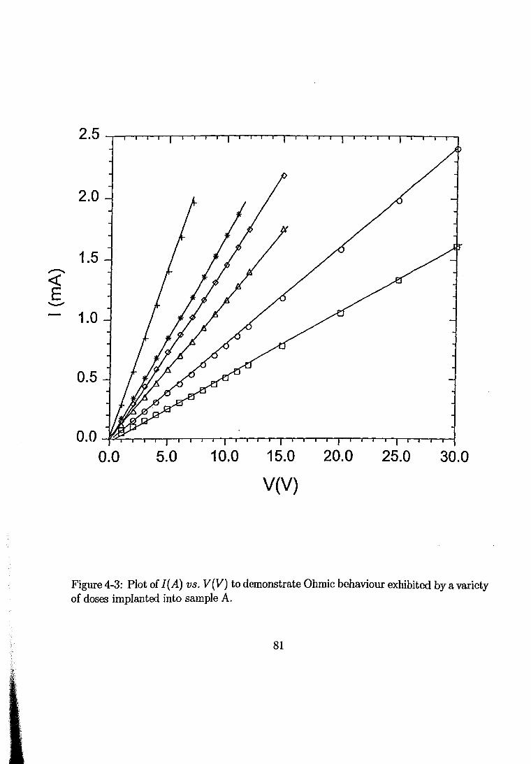
2.0
1.5
1.0
0.5
o.o~~~~~~~~~~~~~~~~~~~
0.0 5.0 10.0 15.0
V(V)
20.0 25.0 30.0
Figure 4-3: Plot of I( A) vs. V(V) to demonstrate Ohmic behaviour exhibited by a variety of doses implanted into sample A.
81

Ion Energy (keY) Dose (cm-2) x 1014
B 130 22.50
110 7.50
90 3.75
80 3.75
70 3.75
60 3.75
50 3.75
40 3.75
30 3.75
Total B-ion dose --+ 6.0 X 1015 cm-2
Ion Energy (ke V) Dose (cm-2) x 1015
c 150 2.44
120 1.586
80 1.342
50 0.732
Total C-ion dose --+ 6.10 x 1015 cm-2
Table 4.2: Energy, boron-ion dose and carbon-ion fluences used to generate Ohmic contact regions on the diamond surfaces. The electrical contacts are spaced about 5.5 mm apart.
82

g ~ ...... ~ ::::: .,-to
c:r ........ P"' co ...... 00 ~ Boron-ion implanted type ITa diamond samples (RECTANGULAR SAMPLES) 00 .,-to ~ ,:::: 0... > :<
Insulating samples
§ 00
~ 0... .,-to
P"' ~ co ......
1-1
Sample Implanted Implanted- ion n estimated Relative Annealing Annealing R ~ cr ' designation ion-dose concentration, n, from SIMS %error temperature period
estimated by results inn (T=300 K) (T=300 K) (T=300 K) 1
g. 0 .......,
e; ...... :::::
~ ~ (j .,-to ........
~ ~ ...... ...... N ~ ~
00 ...... c:r 0
c.J ::::: 0 1-1
\'.l 0
U1 9 ......
TRIM-92 simulation program
x 1015 (cm"2) x 1021 (cm"3) x 1021 (_cm"3t (OC) (minutes) (k.Q) (Q-cm) (Q -cm)"1
AB21 21 1.0 1.02 1.48 1200 5 373 5.09 0.196 AB24 24 1.14 1.16 1.72 1200 5 119 1.63 0.61 AB27 27 1.29 1.31 1.15 1200 5 65.7 0.89 1.12 AB30 30 1.43 1.45 1.38 1200 5 31.5 0.43 2.33 AB33 33 1.57 1.60 1.57 1200 5 20 0.27 3.66
~ 0 :::::
'0 ......
ffi .g 0...
........ ...... a s ~ ~ ...... ~ 0
~ co
~ ~ ~
(1) $;:)
00 0... ......
AB36 36 1.71 1.74 1.72 1200 5 13.1 0.18 5.57 AB39 39 1.86 1.89 1.33 1200 5 8.49 0.12 8.62 AB42 42 2.0 2.03 1.48 1200 5 6.89 9.4 x 10·2 10.63
AB45 45 2.14 2.18 1.61 1200 5 5.92 8.1 x 10·2 12.37
AB48 48 2.29 2.41 5.07 1200 5 4.37 6.0 x 10·2 16.76 AB51 51 2.43 2.56 5.19 1200 5 3.57 4.9 X 10"2 20.51 AB54 54 2.57 2.71 5.30 1200 5 3.49 4.7 X 10"2 20.98 AB57 57 2.71 2.87 5.40 1200 5 2.60 3.6 x 10·2 28.16 AB60 60 2.86 3.02 5.15 1200 5 2.32 3.12 x 10·2 31.56 AB63 63 3.0 3.17 5.25 1200 5 1.81 2.5 X 10"2 40.54
X ~ ~ 0 01 :::::
AB66 66 3.14 3.32 5.33 1200 5 1.77 2.4 x 10·2 43.30 AB69 69 3.29 3.47 5.12 1200 5 1.51 2.1 X 10"2 48.46
X 0... ......, 00
§ s '0
c..> ffi

00 ...... ::::;
X ~
"'"' J:T ~ (:, CD
< 0"' X ...... .........
(") CD tv
...... ~ e.
§~ ~ ~ «: 0 ...... > ~
Samples in the vicinity of the M-1 Transition (RECTANGULAR SAMPLES)
J:T r:tl CD
~ a::: I -~ e;
>-1 «: ~
t5 0 ...... ...... ~ 0"' ......
Sample Implanted Implanted- ion n estimated Relative Annealing Annealing R cr (J
designation ion-dose concentration, n, from SIMS %error temperature period estimated by results mn (T=50K) (T=50 K) (T=l.56K)
TRIM-92 simulation program
x 1015 (cm"2) x 1021 _(_cm-3) x 1021 (cm"3
) fC) (minutes) (Q) (Q-cm)"1 (Q -cm)"1
0 0 ::::; >-1 --- 0
~ 9 ...... p.. 0
::::; .,.,.. ...... 00 g' s ~
...... "t::) >-1 ......... g. ~ e; ~ ~
(")
~ ~
g; ...... "t::) N CD ~ -~ -......
~ 0 ::::; p.. ?l ...... en ~ ~
0 ::::; p.. - r:tl CD
r:tl ~
&. s "t::) s .........
g ffi --...... r:tl 0
~ t5 e; "t::) -('1)
AB72 72 3.43 3.62 5.21 1200 5 5476 13.37 0.14 AB75 75 3.57 3.77 5.29 1200 5 4353 16.82 2.30 AB78an1 78 3.71 3.92 5.36 1200 5 4427 16.7 1.17 AB78anl2 78 3.71 3.92 5.36 1200 30 4599 15.9 1.49 AB78anl3 78 3.71 3.92 5.36 1200 120 3211 22.8 2.50 AB78anl4 78 3.71 3.92 5.36 500 30 2720 26.9 3.68 AB78anl5 78 3.71 3.92 5.36 500 120 3044 24.1 3.54 AB78 78 3.71 3.92 5.36 1700 10 5307 13.8 4.17 AB81anl1 81 3.86 4.07 5.18 1200 5 3602 20.3 0.98 AB81anl2 81 3.86 4.07 5.18 1300 30 4621 15.8 3.7 AB81an13 81 3.86 4.07 5.18 1400 60 4557 16.1 4.7 AB81anl4 81 3.86 4.07 5.18 500 30 4244 17.3 3.7 AB81anl5 81 3.86 4.07 5.18 500 60 5122 14.3 3.4 AB81an16 81 3.86 4.07 5.18 500 120 5306 13.8 4.2 AB81anl7 81 3.86 4.07 5.18 1300 10 2882 25.4 10.4 AB81anl8 81 3.86 4.07 5.18 1400 10 2317 31.6 23.6 AB81anl9 81 3.86 4.07 5.18 1600 10 1099 66.6 26.7 AB81 81 3.86 4.07 5.18 1700 10 505 145 29.4 AB84 84 4.0 4.21 5.25 1700 10 711 103 73.8
*5.5 (mm) is the distance between the two-point electrical contacts
('1) r:tl
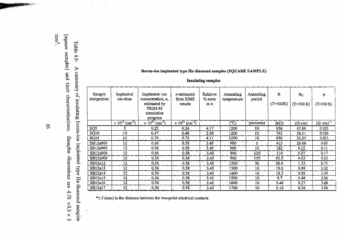
J ... ~,f, ..
s "W s '§ ...,;_] c..o ~
~ '""! ('!) ......... Ul ('!)
.+:o. ~ 01 'E.. .. ffi > ..__..
Ul §
I 0.. c:-t-P"' $. « '""!
0 g. ....., ......
~ ~ ~ e. c:-t- ~ ('!) ...... '""!
~ ...... N Q"q ~ 0"' ......
0 0 00 g 8 Ol
9 ......
Boron-ion implanted type Ila diamond samples (SQUARE SAMPLE)
Insulating samples
Sample Implanted Implanted- ion n estimated Relative Annealing Annealing I
R Ro cr designation ion-dose concentration, n, from SIMS %error temperature period
estimated by results mn (T=300K) (T=300K) (T=300 K) TR.Th1-92 simulation program
x 101' _(_cm·1_ X 1021 (em~)_ X 1021 (cm"3
) COC) (minutes) (kn) (Q-cm) en -cm)"1
SQ5 5 0.23 0.24 4.17 1200 10 856 42.86 0.023 SQ10 10 0.47 0.48 2.08 1200 10 761 38.11 0.026
(f). § ~ ...... s 'E..
'E.. ffi § e: c:-t-
s a ('!)
c:-t-~ ~ ...... 0 ('!) ~ -Ul -
SQ15 15 0.70 0.73 4.11 1200 10 650 32.55 0.031 SB12a900 12 0.56 0.58 3.45 900 5 415 20.66 0.05 SB12a900 12 0.56 0.58 3.45 900 10 182 9.12 0.11 SB12a900 12 0.56 0.58 3.45 900 120 119 5.97 0.17 SB12a900 12 0.56 0.58 3.45 900 150 92.5 4.63 0.22 SB12a12 12 0.56 0.58 3.45 1200 30 26.6 1.33 0.75 SB12a13 12 0.56 0.58 3.45 1300 10 19.6 0.98 1.02 SB12a14 12 0.56 0.58 3.45 1400 10 18.3 0.92 1.09 SB12a15 12 0.56 0.58 3.45 1500 10 9.7 0.48 2.06
~ ~ 0.. ('!) ...... .+:o. ~ :_;, 0 Ol ~
SB12a16 12 0.56 0.58 3.45 1600 10 5.46 0.27 3.66 SB12a17 12 0.56 0.58 3.45 1700 10 5.18 0.26 3.86
-~
*1.5 (mm) is the distance between the two-point electrical contacts 0.. X Ul c.:>
~ 01 X 'E.. c.:> ffi

~ ~ :::l
(!) p.. 00 s ~ X (!) C) C..;! <:"t- .........
~ (!)
Ql ~ Carbon-ion implanted type Ila diamond samples (RECTANGULAR SAMPLES)
X (:) 0')
C..;! 00
~ ~ >
'i:j 00 ......... § <:.> (!) 00 ..__.., ~ s 00 ~ (!) p.. <...c:: ..... 0 :::l ....., <:"t- (:)
l:J"' ~ ..... 00 C) 00 0 <:"t- :::l ~ I p.. .....
0 <...c:: :::l § .....
00 p.. .g 0') <:"t- .........
l:J"' ~ (!) ..... 1-1 (!)
g. p.. <:"t-e; "<
'i:j
~ (!)
<:"t- ~
~ ~
..... ~ N p.. ~
..... ..... s 0 :::l 0 ~ :::l
p.. r::t:J 00 ~ s s
'"0 '"0 ......... ......... ffi (!)
00
Insulating samples
I
I Sample designation Implanted Implanted- ion Annealing Annealing R Ro cr cr ion-dose concentration, temperature period
n, estimated by (T=300 K) (T=300 K) (T=300 K) (T=4K) TRIM-92 simulation program
x 1015 (cm"2) x 1020 (cm"3
) fC) (minutes) (kn) (0-cm) (0 -cm)"1 (Q -cm)"1
C560 5.6 2.61 1200 30 11.81 0.16 6.19 0.69 R2C560 (repeated) 5.6 2.61 1200 30 5.394 . 7.38 X 10"2 13.55 5.08 C565 5.65 2.63 1200 30 24.28 0.33 3.01 2.2 X 10"2
R2C565 (repeated) 5.65 2.63 1200 30 10.65 0.15 6.86 0.39 C570 5.70 2.65 1200 30 14.21 0.19 5.14 1.64 X 10"3
R2C570 (repeated) 5.70 2.65 1200 30 8.94 0.12 8.17 0.924
Metallic Samples I I
C575 5.75 2.67 1200 30 4.69 6.41 X 10"2 15.58 7.9 R2C575 (repeated) 5.75 2.67 1200 30 5.11 6.99 X 10"2 14.3 -R3C575 (repeated) 5.75 2.67 1200 30 2.04 2.8 X 10"2 35.88 20.45 C580 5.80 2.70 1200 30 3.31 4.5 X 10"2 22.09 12.6 C590 5.90 2.74 1200 30 2.11 2.88 X 10"2 34.71 22.0 C595 5.95 2.77 1200 30 0.68 9.28 X 10"3 107.71 88.25 C1425 14.25 6.63 1200 30 0.45 6.20 X 10"3 161.24 139.71
--·--
p.. --..... ..... s :::l
00 (!) e. :::l 00 ~ ..... <:"t-0 ..... :::l ~ 00

4.4 Janis cryostat
The main components that make up the Janis cryostat are the 8l liquid nitrogen and
5l liquid helium reservoirs, both of which are contained in a vacuum jacket. In close
contact to the helium bath is the sample chamber, where the cryogenic probe (sample
holder) freely hangs. The link between the liquid helium bath and the sample chamber
is provided by a needle valve. A cross sectional view of the Janis cryostat is shown in
Fig. 4-4.
Before the initiation of the low-temperature experiment, the vacuum jackets on the
Janis cryostat were first pumped out through the vacuum pumping port, which is at
tached to a diffusion pump, until a vacuum of w-6 - w-7 torr was registered on the
Edwards Penning gauge (model 8). Such a vacuum was achieved after continuously
pumping the cryostat for ,about two days using the two-stage oil diffusion pump backed
by a rotary vacuum pump. The cryostat was then purged with helium and back-filled
with pure helium exchange gas. The purging process was repeated several times even
when the experiment was in progress. This was to safeguard against blockage of the
needle valve by frozen air.
Samples were first cooled down using liquid nitrogen to about 110 K, while maintain
ing the sample chamber and the helium bath pressured to "' 1 atmosphere with helium
gas. When a temperature close to 110 K was reached, liquid helium was transferred
into its 5l main reservoir. The procedure for such a transfer is described later in the
text to serve as a guide towards an efficient running of the cryostat. The liquid helium
was drawn out of the helium bath via the needle valve, through the capillary tube, into
the base of the sample chamber at which a vaporizer was mounted. The vaporizer was
connected to an external power supply, of which a maximum of 2 V could be used for a
87
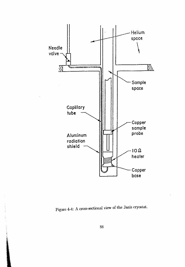
Needle valve
Capillary tube
Aluminum radiation shield
Helium space
\
Sample space
Copper sample probe
10 .n heater
Copper base
Figure 4-4: A cross-sectional view of the Janis cryostat.
88
safe operation.
The rate of cooling of samples, which is achieved by an upward evaporation of helium
vapour, is determined by three factors:
1. • The amount by which the needle valve is opened. A quarter of a full turn is
recommended for measurements at T >50 K, or can be adjusted as desired.
• The energy supplied to the vaporizer by the power supply. This energy should
be reduced systematically by decreasing the voltage on the power supply from
2 V to 0 V for the conductivity measurements at T :::; 50 K.
• The energy supplied by the mounted heater on the sample probe. The heater
range is selected on the Lakeshore temperature controller. A 100 n heater
used in this work provided a maximum power output of 25 Watts, as the
compliance voltage of the temperature controller is 50 V and the maximum
current that one can use is 1 A.
Keeping the needle valve free to turn about and the capillary tube unblocked are the
main concerns before the liquid helium precooling procedure. By following the procedure
as described in the point-form below, I managed to achieve a success rate of over 95%.
4.4.1 Maintenance of the Janis cryostat
Before the cryostat was used, a check was made to detect any collection of water or ice in
the nitrogen reservoir from the previous run. If any was found, it was sucked out using
a sponge mounted at the end of a long thin rod. This involved dismounting one metal
seal that covered the top of the cryostat. When all the water had been cleared out, a
latex transfer line was connected to a nitrogen gas cylinder and one end inserted to the
89

base of the nitrogen bath. A small nitrogen gas flow was used to dry out any remaining
water droplets.
4.4.2 A procedure for the running of the Janis cryostat
Fig. 4-5 and Fig. 4-6 show different views of the cryogenic system where all the com
ponents are labelled for the description below. The procedure to run the Janis cryostat
includes the following steps:
All the nitrogen cold-traps connected to the Janis cryostat have to be filled prior to
the running of the Janis to avoid hot oil vapour back-streaming into the vacuum jackets
and the liquid helium space, with the latter leading into the sample chamber.
• Open the exhaust valve (glass valve) (A) and close the main valve (B) leading to
the recovery line. This is to avoid transmitting an exhaust gas down the recovery
line to the helium plant, or sucking in dirt from the recovery line into the cryostat.
• Isolate the liquid helium bath and the sample chamber by closing the needle valve
(C) and the 'main regulator' valve (D). Both the sample chamber (E) and the
helium reservoir (F) will now be under vacuum.
• Backfill the cryostat with pure helium gas, while keeping either the sample chamber
or the helium reservoir under vacuum.
• Open the needle valve and monitor the pressure gauge mounted on one of the valves
(G). If the pressure variation is observed on the pressure gauge, it means that the
needle valve and the capillary are free and unblocked.
• Liquid helium can then be transferred into its main reservoir.
90
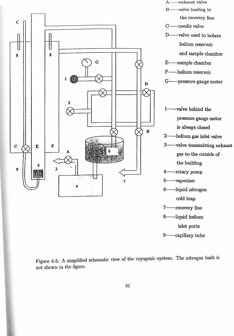
c
8
c
9
8
1
2
7 • 4
A--exhaust valve
B--valve leading to
the recovery line
C--needle valve
D--valve used to isolate
helium reservoir
and sample chamber
E--sample chamber
F--helium re8ervoir
G--pressure gauge meter
1-valve behind the
pressure gauge meter
is always closed
2--helium gas inlet valve
3--valve transmitting exhaust
gas to the outside of
the building
4--rotary pump
5--vaporizer
6-liquid nitrogen
cold trap
7--recovery line
8--liquid helium
inlet ports
9--capillary tube
Figure 4-5: A simplified schematic view of the cryogenic system. The nitrogen bath is
not shown in the figure.
91

To Helium To Pump Recovery
Fill Port (~'1~ ® ""----4~'-.A-__J r----'vxr
_..I L.-~ 1-----...J ..... _ ....
Helium Space
Vacuum Space
Sample Space
~t't ~ Capillary
Needle Valve
Tail of Dewar
~ ~ Electromagnet
Figure 4-6: A simplified schematic view of the Janis cryostat. The nitrogen bath is not
shown in the figure.
92

4.4.3 Cryogenic sample probe
A schematic view of the cryogenic sample probe is shown in Fig. 4-7. Mounted on
the cryogenic probe is a carbon glass thermometer (model CGR-1-500) which has been
calibrated by Lakeshore in the temperature range 300-1.56 K. An Alan Bradley resistor
has been mounted just above the sample in order to monitor the level of liquid helium in
the sample chamber. This is necessary when we have to carry out transport measurements
below 4 K. In this case, we have to pump on the liquid helium to reduce its pressure.
Wound at the base of the probe is a 100 n heater to help us fine tune the cooling rate.
A number of breathing holes were made through the copper block to allow liquid helium
into the sample can, and to let electrical leads run out of these holes to the ten pin
connectors situated at the top of the cryogenic probe.
Thermal anchoring of samples to a copper substrate is provided by a low-temperature
vacuum grease. To do this, I applied a thin layer of Apiezon vacuum grease or Dow
Corning vacuum grease on a cigarette paper and placed a sample on top until it dried.
Baking in an oven set at 60 oc for some time can also help in solidifying the vacuum
grease. The sample was wrapped with a teflon tape to avoid contamination on the
surface. The sample holder was then screwed on to the same copper block to which the
carbon glass thermometer was mounted. Anchoring of the thermometer to the copper
block is achieved by means of the leads. Initially, the leads were wound round a copper
slab specifically designed for this and then covered with a thick varnish layer. Recently,
the electrical leads of the carbon glass resistor were sandwiched between the gold plate
metal slabs and anchored to the copper block. This was to avoid having to unwind the
thermometer leads every time we exchanged the cryogenic probes with other workers.
Some nylon spacers were placed around the probe to help keep the probe in a clearly
vertical position. Orientation of the sample is important when conductivity measure
ments are to be made in the presence of a magnetic field. In this case, samples were
93

-t--------------------0-ringSeu
--+----------Main Cryostat Mounting Cap
:>--------·'"'·& .... Stainless Steel Coax.
+---------Thermometer Anchoring Post ~..,..1-J...... ~--H-----------------~~wcfur~rot~nngTheonmn~er
-lB--H--------Oopper Block
n--------Radiation Shield
Figure 4-7: A schematic view of the cryogenic probe used to mount samples.
94

oriented perpendicular (i.e. transverse) to the field.
4.4.4 Temperature controller and the Keithley electrometer
The sample temperature is monitored and controlled with the use of a Lakeshore temper
ature controller, model DRC-93A. The controller monitors temperatures by comparing
the actual sensor voltage or signal with an analog voltage created by the unit which cor
responds to the user's desired temperature or set-point. The controller is able to stabilize
temperature to within 1 mK.
Highly resistive samples were measured using a Keithley electrometer, model 617.
The Keithley electrometer affords us the means to measure samples up 1016 n, but, due
to huge fluctuations in the resistance of our samples, we decided to analyze only the R-T
data measured up to 1011 n. We tried screening the current and voltage leads as well as
the measuring instruments but it did not help us much. The maximum current that one
can use is 2 rnA, while the measuring range of voltage is ±102.40 V. The voltages that
I used for carrying out conductivity measurements were in the range 2-10 V. A Fluke
digital multimeter (model8840 A) was used for some samples which showed metallic-type
conduction.
4.4.5 Low-temperature electrical conductivity measurements
The low-temperature electrical conductivity measurements were carried out using the
Janis cryostat and the dip measuring system. Since we started with highly insulating
samples, only two-point conductivity measurements were carried out using the Janis cryo
stat. As the samples became more and more metallic, subject to further implantations,
we switched over to the four-point electrical contact measurement technique, and the dip
system was then used.
95

I briefly describe the experimental process involved in measuring transport in samples
using these techniques. I describe first the Janis cryostat procedure.
A typical low-temperature run proceeds as follows. The sample probe is first con
nected to the data capturing system, the temperature controller and the Keithley, or
the multimeter electrometer devices, via the IEEE interchange bus. The cryostat is first
purged, as described under the maintenance section, and the nitrogen pot filled. The
dewar is then left to cool overnight. The needle valve is kept closed so that no liquid that
can have found its way into the helium space can enter the capillary tube and the sample
chamber. Such a possibility is remote except when liquid nitrogen has been transferred
into the helium bath (and then removed) to achieve a faster cooling rate. After about 10
hours, the temperature of the cryogenic system will have reached 110 K. At this point the
helium reservoir and the sample space are both purged and backfilled with pure helium
gas. The needle valve and the capillary tube have to be clear of any blockage. If any
blockage is detected, the experiment has to be aborted by warming the cryostat to room
temperature for maintenance. With the needle valve still closed, a transfer of liquid he
lium into the helium bath is carried out. The rate of liquid helium transfer is monitored
by a helium meter gauge mounted on the helium recovery line. On average, two litres
of liquid helium are lost to the recovery line by boil off during a fill. After the transfer,
the needle valve is opened as desired to allow liquid helium to gather at the base of the
sample space. Because of the location of the sample chamber in relation to the helium
can, the flow of helium from the main helium bath into the sample chamber is mediated
by gravity. A faster transfer can be induced if a pressure differential between the he
lium bath and the sample chamber is maintained. This can be achieved by evacuating
the sample space with the needle valve kept wide open, while maintaining the helium
reservoir at atmospheric pressure.
96

After collecting about a litre of liquid helium into the sample space, a process that can
last about an hour, the needle valve was closed and the sample space isolated. The sample
chamber was then pumped with a rotary pump connected directly to the sample chamber.
The cooling rate depends on the pumping speed and the input heat by the vaporizer
or heater mounted on the probe. Much practice is needed to control the temperature
efficiently with sufficient accuracy. To cover the temperature range 1.56 to 4.02 K, it
usually took over an hour to obtain reliable data, which in most cases were reproducible.
In order to measure samples on the way up, the pumping speed was systematically
reduced and vaporizer turned on to fine tune the temperature. In this case, cooling of
samples is achieved via the helium vapour. The needle valve was kept closed until a
temperature of 4 K was reached, and then opened to about a 1/8 of a full turn to allow a
steady inflow of liquid helium into the sample chamber. Mter a successful run, samples
can be replaced with new ones by pulling out the sample probe without having to warm
the cryostat to room temperature. With the probe taken out, the sample chamber is
over-pressurized with helium gas and the chamber closed by a rubber stopper.
4.5 The dip measuring system
Before running the dip system, the cryogenic probe, which is sealed with a stainless
steel tube, is evacuated using a single stage rotary pump and backfilled with a pure helium
exchange gas. This is to avoid condensation on the surfaces of the mounted samples even
though precautionary measures of wrapping samples fully with teflon tape are applied.
The typical temperature range over which the electrical conductivity measurements can
be made is 4.5 to 300 K. On average, a complete run takes about 5 hours when a cooling
rate of one degree per minute is maintained.
97

Four-point resistivity measurements on our samples were performed by slowly lowering
the cryogenic probe in a liquid helium dewar. The rate of insertion of the probe to the
helium reservoir is controlled by a home-built motor-lowering device. In the case of highly
insulating samples, a two-point configuration Keithley electrometer (model 617) is used
to measure the voltage across the sample with a known constant current flowing through
the sample. The sample temperature is obtained with the use of a Rh/Fe resistance
thermometer connected to the Prema digital voltmeter, model 5000. The resistance
of low resistive samples is determined by measuring the voltage across the sample, also
employing the Prema digital voltmeter, but the current is determined using two standard
resistors (each of resistance of 98 n). In some cases, an external buffer resistor has to be
added to obtain the desired current through the sample. The cryogenic probe is similar
to the one used in a Janis cryostat but with some modification.
The details of the dip system can be found in a number of standard cryogenic books on
low-temperature cryogenics. The following books, written by Richardson[l40], Betts[l41]
and Kent[142], have been found useful in introducing the writer to this field.
4.6 High-temperature conductivity measurements
The two-point electrical conductivity measurements were extended to temperatures
up to 773 K. These measurements were sufficiently accurate for the purpose of our study
in trying to measure the activation energies at high temperatures. We could not carry
out the 4-point electrical measurements due to the experimental difficulties encountered
with our measuring system. Platinum wires were used as measuring leads, by running
them through the ceramic tube which has two open-ended separate holes. A sample
98

holder was made up of a stainless steel plate punctured with four holes to accommodate
stainless steel screws. Platinum wires were put on the baked contacts and supported in
place by a piezoid quartz plate, which had been cut to dimensions 12 x 12 x 3 mm3 . Fig.
4-8 shows a schematic view of the sample holder.
After a sample was mounted, it was sealed inside a stainless steel tube. Before the
initiation of the experiment, this 'mini cryostat' was purged and backfilled with inert
ultra pure argon gas. During measurements, the sample was continuously flushed with
argon gas to inhibit surface graphitization. The inflow of argon into the cryostat was
monitored by dropping one end of the latex transfer line into a beaker filled with water.
A home-built oven, made up of asbestos and covered by a metal shield, was used in
this study. A RKC (model Rex P9) 8 step programmable temperature sensor was used
to control the system's temperature, with a J-type iron and constantan thermocouple
connected to an oven. As a form of precaution, this oven was rested squarely on ceramic
blocks.
The sample resistivity was measured with the use of a Keithley electrometer. Fig.
4-9 shows a block diagram of the measuring system employed in this study. Electri
cal contacts have been prepared using two different procedures. The first procedure
involved implanting the ends of the diamond specimens with boron ions, as described
in earlier sections, and then evaporating a layer of gold onto the implanted electrodes.
Another method involved the use of silver paint covering the same region as the im
planted contacts, so that the same sample geometry is maintained. The silver paint was
then annealed to 70 oc for at least two hours. This method was put into use after we
encountered numerous problems with the first one. We have observed that, at T > 773
K, the implanted contacts were etched out of the diamond layer, taking with them some
of the implanted boron-ion conducting layer. We measured this sample again at low
temperatures and recorded a slight increase in its resistivity. Since we were uncertain
99

I~
... ~
""' ~
'---
+--
Ceramic rod
J-type Iron-constantan thermocouple
Stainless steel sample holder
-...~r-=:::=::::::==-- Platinum wires
Piezoid quartz plate
Diamond specimen
Stainless steel screws to hold the quartz plate and diamond in place.
Figure 4-8: A sample holder used in the study of high-temperature conductivity mea
surements.
100

about the actual boron concentration in these samples, it was decided that they had to
be repolished. An alternative way would have been to carry out the SIMS analysis-a pro
cedure we could not follow due to time constraints, Besides this setback, the evaporated
gold strips were completely burned out at T around 773 K. Occurring concomitantly
with these incidents was the recorded stray conductance of ceramic, shorting the circuit
of our system. Due to these multiple problems, we decided to limit our conductivity
measurements to 773 K.
101

Temperature Annealing
sensor Furnace
Keithley Diamond Beaker with water to electrometer Specimen monitor argon gas flow
Ultrap-pure argon gas cylinder
Figure 4-9: A block diagram of the conductivity setup for high-temperature conductivity measurements.
102

Chapter 5
High-temperature annealing results
5.0.1 Motivation
A major objective of the present work is to find ways in which we can optimize the
implantation-annealing parameters so that we can activate as many of the implanted
boron ions into substitutional sites as possible. Our approach is based on the experimental
observations made by various authors [5, 120] about the behavior of boron atoms in ion
implanted damaged layers in diamond. It has been found that more and more of the
implanted boron-interstitials diffuse out of the damaged cascade when the annealing
temperature is increased[120]. This is in clear contrast to the behaviour of carbon self
interstitials[131]. Our expectation is that the probability of self-interstitials recombining
with vacancies should grow as the annealing temperature is raised.
We have studied effects of high-temperature annealing on boron-ion doped layers in
diamond. This study was carried out by monitoring the electrical resistance as a function
of dose and annealing temperature. A wide range of samples implanted progressively
from the insulating regime to the vicinity of the metal-insulator transition, using the
multiple-step CIRA technique, were used in this study.
103

5.1 High-temperature annealing results
Fig. 5-1 shows plots of electrical resistance vs. cumulative boron-ion doses following an
nealing at 1200 °C. The results were taken at three temperatures, shown in the figure, to
demonstrate saturation effects of the point-defects within the ion-implantation damaged
layer in diamond. It is apparent in the figure that as the boron-ion dose is increased
in the damage cascade, the resistance-dose curves tend to saturation (asymptotic) limit
with R rv 1 K!l
Fig. 5-2 and Fig. 5-3 show plots of resistance vs. temperature for samples AB81 and
AB84. These samples have been subjected to anneals at temperatures above 1200 °C.
As seen in the figures, the resistance of the samples decreases with increasing annealing
temperature. Several reasons which can account for a decrease in the sample resistivity
have been suggested. Some of these reasons include the following: the removal or dimin
ishing effects of compensating donors including vacancies and/or a decrease in Anderson
disorder (see chapter 2) in this system. We report further on this issue in the discussion
section below. As a point of caution, we could not anneal our samples beyond 1700 oc due to the possible graphitization of the implanted layer, particularly for samples which
were implanted quite close to the metal-insulator transition. Actually, some of the sam
ples developed a milky colour on the implanted region even when annealed below 1700
°C. In these samples some of the boron-ion doped layers were partly etched out. So we
had to repolish the doped layer and start all over again.
The resistance against annealing temperature plots for samples AB81 show a steady
drop in resistance with increasing annealing temperature. A drop is expected as long
104

Q) 0
11,-------------------------~
8
6
6 -----4 K
D -----77 K
0 ----300 K
3+-----~--~~~~~~ 2 4 6 8
Dose ( 8-ions I cm2) x 1016
Figure 5-1: Plots of electrical resistance vs. cumulative boron-ion dose. Samples have been annealed at 1200 oc for 5 minutes.
105

§ 0 ..ca:<(:..---- 1200 c
~--l=.----1300 c ++!fl.p
X X + 8J. + dJ -1:: rt- + + X X X X 0 0 + J + ++ + + + + +
'(xxxxxx 0 0 ... ~1500 C X X X X X X x
0x
•••••• 7
~-·········· "-1600 c ••••••• I e ~ e e e e e e e e e
"'1700 c
102 ~~~~~~~~~~~~~~~ 0 10 20 30 40 50
T (K)
Figure 5-2: Plots of R vs. T for sample AB81. This sample was annealed over various
temperatures shown in the figure.
106

~ c ......._,
~
650
' 0 600 0
0 0
0 0
0 550 0
0 0
0 0
0 0
500 0 0
0 0
0 0
0 0
450 0
0 10 20 30 40 50
T (K)
Figure 5-3: Plots of R vs. T for sample AB84. This sample was annealed only at 1700 oc after the CIRA routine.
107

as compensating centres (and/ or lattice disorder) are not completely eliminated in this
system. Such a possibility (of effectively removing the compensating centres) seems
remote in our case owing to the constraints related to annealing under which we have to
work. This is also compounded by the fact that diamond is thermodynamically unstable,
and can transform permanently to graphite at high-temperatures.
As a fore-runner to the discussion of the experimental results, I give a review of
pertinent models which apply in the case of doped diamond.
5.2 Theoretical model for the point-defects
Prins[120] has outlined a theoretical model to describe the interstitial-vacancy re
combination in an implanted surface layer in diamond during the annealing process. The
main purpose of this model is to demonstrate the importance of multiple ion-implantation
steps in order to circumvent graphitization of the implanted layer on the diamond surface.
During a high-temperature annealing cycle (on a diamond specimen that was im
planted at liquid nitrogen temperature), there will be a continuous dynamic recombina
tion of the point-defects, with self-interstitials recombining with vacancies and dopant
interstitials combining with some vacancies. Some of the dopant-interstitials may diffuse
out of the implanted layer before recombining with vacancies.
Let the number of interstitials and vacancies created per implantation dose, step J,
of ions per unit area, be aJ, where a is the average number of atoms displaced from
their lattice positions by a projectile ion. From previous anneals, we would have some
residual vacancies, nvr, remaining in the damage cascade. Prins showed that the residual
108

vacancies nvf remaining after the next annealing step can be given by[120],
where Ti is given by
[ aJ KTil nvf = (nvr + aJ) exp -~
2
Ti = ~ (w + 1)-1
<p
with w = aJ - 1. In the case of dopant ions, it can be shown that(123) n,,-n,r
(5.1)
(5.2)
(5.3)
where r is a constant. The ratios for the self-interstitial-vacancy recombination and
dopant-interstitial-vacancy combination have been derived by Prins[l20), respectively as
( 1) -I Rc = 1 + W (5.4)
and
( rr Ra = 1 + 'lJ (5.5)
Analysis of Eqs. (5.4) and (5.5) will help us gain some insight into the damage cascade.
This is discussed in section 5.6.
5.3 Discussion
5.3.1 Multiple CIRA sequences
It has been established recently that effective control over the distribution and interac
tions of point-defects in the ion-damaged layer can be gained by multiple-implantation
109

sequences[120, 123]. We consider this claim from a theoretical point of view. The main
important theoretical predictions derived from the point-defect interaction model are,
( r)-1
Ra= 1+'11 (5.6)
where '11 = a.J - 1. If the factor nvf - nvr is kept small, ideally zero, for small nvf-nvr
implantation steps, then the activation energy increases and more of the implanted boron
ions combine with vacancies (residual and newly created) during the follow-up annealing
cycle. This means that W will be large and Rc and Ra will approach unity. For the latter
to be close to unity, the term r must be small. This procedure justifies the use of small
dose steps, which introduce small numbers of vacancies into the damaged layer and keep
nvf just slightly bigger than nvr. In other words, multiple implantation steps introduce the
implanted ions into an area which already contains vacancies, increasing the probability of
vacancy-interstitial recombinations. By following this procedure, the vacancy threshold
beyond which the implanted diamond surface layers will be transformed to graphite can
be avoided.
5.3.2 Residual damage saturation
The TRIM-92 computer simulation program has been used to further probe the genera
tion of residual damage for multiple implantation-annealing sequences. For a boron-ion
implantation into diamond, TRIM-92 indicates that the average number of vacancies
produced per ion is 183 for an ion accelerated into the target at 120 keV. For diamond,
the displacement energy is 35 eV and the binding energy 5 eV. Since a large number of
vacancies are generated, they would outstrip the activated dopant-interstitial atoms in
the damaged region. The difference becomes even larger following the next implantation
annealing cycle. As more boron ions are implanted into the damaged cascade, the residual
damage starts to saturate. We expect the probability for boron activation to increase in
llO

the already saturated layer. Table 5.1 shows the energies, ion dose and the generated
vacancies in diamond.
5.3.3 Activation of boron ions in implantation-damaged layers
Fig. 5-4 shows plots of the electrical resistivity vs. inverse temperature for sample
DB12 (square sample) annealed at 1300 oc, 1500 oc and 1700 °C. The sample has been
implanted to a total dose of 1.2 x 1016 cm-2 (rv 4.8 x 1021 cm-3). It is difficult from Fig.
5-4 to fit straight lines to determine slopes and hence determine the activation energy
over the entire temperature range measured. This means that transport in this system
is not activated but occurs via non-nearest-neighbour hopping sites. It has been argued
that these hopping centres may be associated with excess vacancy clusters (agglomerates)
which have been dispersed randomly in the ion-damaged layer[128, 143, 144).
Our experimental results do not indicate that more of the subsequent implanted
boron atoms escape the damaged layer during high-temperature annealings, as reported
recently by Prins[120) on similar systems. This may indicate that boron atoms become
even more 'severely' compensated upon further ion implantations.
111

Ion Energy (ke V) Dose (cnc2) x 1014 vacancies (cm-2) x 1016
B 130 11.25 20.6
110 3.75 6.49
90 1.875 3.13
80 1.875 3.02
70 1.875 2.74
60 1.875 2.57
50 1.875 2.34
40 1.875 2.08
30 1.875 1.78
Total --t 3.0 x 1015 cm-2 4.17 X 1017 cm-2
Table 5.1: Ion energies and ion doses used to generate a boron-ion layer in a diamond specimen. The created point-defects are homogeneously distributed in the implanted layer. The vacancies created following each implant have been calculated using the TRIM-92 simulation code in which the displacement energy of 35 eV and the lattice binding energy of 5 e V were assumed.
112

286
T(K)
250 222
/ 1300 °C
200
103 ~--~~-.~-..-.-.-~~~~~~~~
3.0 3.5 4.0 4.5 5.0
1 000/ (T (K))
Figure 5-4: Plots of R vs. 1/T for sample DB12 (square sample) annealed at 1300 °C, 1500 oc and 1700 °C.
113

5.4 Summary
Optimization of different parameters to get high quality and reproducible boron-ion
doped layers in diamond is the key in this study. This involves carrying out multiple
post annealing cycles at high-temperatures following the CIRA steps. We have done this
to a number of samples which have been implanted with low boron-ion doses, and to
some samples implanted closer to the amorphization threshold value. Both experimental
observations and theoretical predictions render a consistent picture on the nature and
behaviour of residual point-defects in ion-implantation radiation damaged layers.
We started annealing our boron-ion implanted diamond ( <>C:B ) samples at 1200
C until a total boron-ion dose of 7.8 x 1016 cm-2 was reached. To reach this dose
level, a multiple CIRA routine was used and the dose spread out in small energies.
The total dose administered to the sample per CIRA treatment was 0.3 x 1016 cm-2.
The annealing cycle was limited throughout to 5 minutes. Annealing over extended
periods had an insignificant impact on the experimental results. We carried out a SIMS
analysis on this sample to determine the concentration of boron atoms in the surface
layers. SIMS measurements estimated the concentration to be rv 3.6 x 1021 cm-3 , which
corresponds to the dose level of 7.3 x 1016 cm-2. This means about 94% of the implanted
boron atoms were "locked-in" the implanted layer. We managed to trap almost all the
implanted boron-ions in samples that have been implanted deep in the insulating side of
the transition.
After reaching a residual damage saturation in some samples which have been heavily
implanted, we carried out some post rapid temperature anneals. Samples were annealed
from 1200 oc to 1700 oc for ten minutes at each temperature in incremental steps of 100
°C. The results are shown in Fig. 5-2. It can be seen from the plots that the resistance of
these samples decreases with increasing annealing temperature. A decrease in resistance
114

indicates two phenomena: an efficient activation of boron interstitials accompanied by
a self-interstitial-vacancy recombination to further reduce the lattice damage, and, sec
ondly, a reduction in the electrical activity of excess vacancy agglomerates. At 1700 oc, a major fraction, if not all, of the boron atoms would have combined with vacancies.
Some samples, particularly the insulating ones, were annealed at 1200 oc followed by a
1700 oc anneal, and a significant drop in resistance was observed.
In brief, high-temperature anneals following the cold-implantation process has pro
vided further insight into the nature, interaction and behaviour of point-defects within
the damaged cascade. The complexities associated with these point-defects are still being
studied.
115

Chapter 6
Percolative transition in carbon-ion
implanted type Ila diamond
Electrical conductivity studies on diamond single crystals, implanted with carbon ions
using the CIRA technique, have been carried out as precursors to the study of electronic
properties of boron ions in diamond. The objectives of the work presented in this chapter
are to demonstrate the importance of multiple implantation steps in the characterization
of diamond samples, and the sensitive dependence of the conductivity on the type of ion
one uses in the implantation process.
6.0.1 Motivation
Implanted layers created with carbon ions using the CIRA routine for ion doses exceeding
the critical threshold dose are the subject of the present investigation in type II a diamond.
This work also explores transport phenomena in the vicinity of the M-I transition, and
deep into the insulating phase in which a low-temperature conductivity crossover between
the Mott VRH and Efros-Shklovskii VRH is demonstrated.
116

6.1 Introduction and a general overview
The transformation that a natural diamond crystal undergoes, from a purely insulating
state into a highly conducting form of carbon, as a result of ion-implantation, has been
studied for many years. Early pioneering work on ion implantation has been carried
out by Vavilov et al.[116] , who implanted their diamond specimens with a variety of
ion species and monitored the changes in the electrical conductivity, /J.a, as functions of
dose and temperature. General surveys which include in-depth discussions, figures and
models which offer insight into the processes involved in the implantation and annealing
can be found in a recent book by Dresselhaus and Kalish[5], and in comprehensive review
articles by Prins(118] and Kalish[145, 146, 147].
Studies reveal that the transformation of diamond, subject to ion implantation, is not
a sudden process. The diamond structure undergoes a transitional state in which it is
first transformed to an amorphous phase ( a-sp3) and then collapses into an amorphous
sp2 graphite phase (a-sp2). The difference between these amorphous carbon states is that
the a-sp3 state is highly insulating and still has characteristic properties similar to those
of amorphous diamond(146], whereas the a-sp2 graphitic state is a highly conductive
form of carbon. The conversion from a-sp3 to a-sp2 occurs at doses far exceeding those
required for a-sp3 amorphization. Kalish(146] has listed a number of factors which inhibit
the immediate graphitization of diamond during ion implantation. These factors include
the following:
• The transformation of a diamond crystal into a graphitic form is governed by an in
crease in density of defects(143]. The density of defects is determined by the amount
of energy transferred during nuclear collisions to each target atom, and the implan
tation temperature. The volume density of point defects is cumulative, since each
ion, irrespective of its energy, cannot by itself induce surface graphitization[146].
This means that the implanted volume has to be hit several times by a number of
117

projectile ions. It is then on further implantations, and the breakage of more a-sp3
diamond bonds, that the affected volume spreads out to form a 'sea' of sp2 graphite
bonds.
• There should be a threshold damage level (i.e. a critical ion dose) in implanted
diamond beyond which the diamond structure cannot be recovered any further
even by high-temperature annealing, but will instead transform to the graphite
phase[145].
Some notable changes occur as the diamond transforms into a graphitic form. These
changes include the following:
(i) a large increase in the electrical conductivity,
(ii) a decrease in material density,
(iii) a mechanical weakening of the diamond,
(iv) the appearance of new optical absorption lines and
(v) changes in chemical properties. (Graphite is etchable while diamond is chemically
inert to aggressive acids.)
All these changes that diamond undergoes as a result of implantation have been
discussed by a number of authors in the book on diamond properties edited by Field[3].
Early work, similar in some respects to that reported in this chapter, has been carried
out by Hauser et al. [128], in which they measured the electrical conductivity in carbon
ion implanted diamond specimens over the temperature range 20-300 K. Their work on
diamond is reviewed below.
Hauser and co-workers[128, 144] have implanted diamond specimens at "' 295 K
(room temperature) using carbon-ions. They selected doses ranging from 3 x 10¹⁵ to
6 x 1016 cm-2 , spread over energies 70, 40 and 20 keV to create a fairly homogenous
118

carbon implant profile in their specimens. The thickness of the implanted layer was
estimated to be "" 100 nm. They measured the temperature-dependent resistivity p(T)
from room temperature down to 20 K. The results from their second publication[144] are
shown in Fig. 6-1. Their data follow the phonon-assisted variable-range hopping (VRH)
conduction process[8] over the measured temperature range. (See chapters 2 and 8 for
discussions on VRH conduction mechanisms.) A departure from this transport process
occurs for the lowest dose near room temperature, in which case the resistivity follows
a thermally activated process with an activation energy, extracted from the data, of 1.7
eV. For the highest implanted carbon-ion doses, the authors have observed metallic-type
conduction close to that of graphite. It was concluded from these measurements that a
large increase in the electrical conductivity may be related to the formation of sp2-bonded
microcrystallite graphitic islands (regions or clusters)[148] in diamond, and that these
graphitic islands act as the hopping centres. However, from the hardness measurements,
Hauser et al. found the implanted layers to be still diamond-like in mechanical properties.
Prins[119] has shown that for carbon-ion implanted diamonds, there is a critical im
plantation threshold beyond which the properties of the implanted layer change in a
dramatic fashion. The CIRA layers take on a dark colour and the electrical conductivity
increases very rapidly in the interval5 x1015 cm-2 to 6 x1015 cm-2 for c+-ions. The
properties of layers generated in this way are highly reproducible with ion dose[149, 150].
A different approach to the onset of conductivity in carbon-ion implanted diamond
specimens was proposed by Kalish et al.[143]. Their recent work in this direction has
been published in refs.[129, 145]. Kalish et al. implanted a number of species into dia
mond crystals held at various temperatures. They found that the electrical conductivity
changes dramatically with increasing dose in the vicinity of the critical dose, De, and
that a(T, D) follows a sharp percolation transition for samples implanted at elevated
temperatures. In the case of carbon implants, they found that a vs. D was not sharp
119

-E ()
>!::: > -r-(f)
(f) w a:
TEMPERATURE (K)
1010 300 93 32 19
0.24
, , , , , , , , " " "'
, ,
, , ,
, ,
C + DOSE (em -2)
• 3.0 X 10¹⁵
0 6.0 X 10¹⁵
• 1.2 X 10¹⁶
0 3.0 X 10¹⁶
A 6.0x1o16
A AMORPHOUSCARBON FILM SPUTTERED AT 95 K AND ANNEALED AT 300 K
- - - AMORPHOUS CARBON FILM EVAPORATED
AT 300 K
0.32 0.40 0.43
TEMPERATURE TO THE POWER-} (K-\)
Figure 6-1: The resistivity data of Hauser et al. [141] described by the Mott VRH relation
over the temperature range 20-300 K.
120

enough to be accounted for by either a sharp percolation transition or a critical energy
density amorphization model for the transition.
6. 2 Percolation theory
Percolation theory is one of the mathematical techniques widely used to analyze
transport phenomena in spatially random systems. The origin of percolation theory is
attributed to Broadbent and Hammersley[151] who introduced lattice models for the
flow of a fluid through a random medium and argued, using probabilistic and geometric
concepts, that no fluid will flow if the concentration of active medium (pores) is smaller
than some nonzero percolation threshold value. A percolation threshold is a point of
the transition between states of short-range connectivity and long-range connectivity
in which properties of a percolation system suddenly change when a concentration of
conducting sites is continuously increased. General applications of the percolation theory,
in a variety of systems, can be found in review papers[152, 153, 154, 155) and a recent
book by Stauffer and Aharony[156).
According to the percolation theory, two distinctive electronic conduction regimes can
be identified depending on the concentration (volume fraction) of the conducting bonds
or sites cf>. When cf> is large, conducting centres form a connected metallic network so that
electrons can percolate directly through the metallic connected pathways. In this metallic
regime, the microgeometry (i.e. size, shape and orientation)[157, 158, 159, 160, 161, 162)
of metallic channels plays an important role in the actual sample conductivity. When
cf> is small, the metallic conducting centres are randomly distributed in an insulating
matrix. Transport of charge carriers between the localized metallic clusters, dispersed in
this dielectric regime, is mediated by phonons. The two conduction regimes (metallic and
121

insulating) are characterized by a percolation threshold at which the conducting metallic
backbone first becomes disconnected. Kalish et al.[143J have presented the above scenario
in a very interesting and elementary fashion.
In the vicinity of the percolative metal-insulator (M-I) transition, the de-conductivity
between any nearest neighbour conduction sites is described by the relation
(6.1)
where a0 is a proportionality constant, ci>e is the critical metallic volume fraction of
the dopant carbon ions and v is the critical exponent which depends on the sample
dimensionality. This exponent indicates whether the M-I transition is driven by disorder
with 0.5 < v < 1, or is forced by geometrical constraints leading to a classical percolation
threshold at ci>e with 1.5 < v < 2(163, 164]. The v values have been found to be system
dependent[165, 166].
According to Kalish et al.[143], the percolation conductivity within the framework of
the effective medium theory can be expressed as
(6.2)
where a0 is the conductivity of the amorphous regions, B = 1/2 in 2-dimensions (2-D) and
B = 2/3 in 3-D, while De is the critical dose level for the onset of metallic conductivity.
Equation (6.2) is only valid at D >De (i.e., above ci>e), and can also be written as[129]
(6.3)
where Rs is the saturation resistance at high doses. We have used Eq. (6.3) to analyze
our experimental data.
122

6.3 Experimental results
Fig. 6-2 shows plots of electrical resistance against temperature for various carbon
ion implanted diamond specimens. The carbon dose level that we have studied spans the
range 5.60- 5.95 x1016 cm-2. In spite of the narrow range of the dose level measured,
Fig. 6-2 shows a dramatic drop in the electrical resistance of five orders of magnitude at
low temperatures.
It is now an established practice to plot R vs. r-m (where m = 1/4 and 1/2) to
determine which of the VRH laws best describes the experimental data. Though the
method is not very reliable due to its applicability over a small experimental R- T data
region, it nonetheless remains a useful tool to probe the nature of the VRH behaviour
in doped semiconductors. Plots generated using this procedure are shown in Fig. 6-3.
It is evident in Fig. 6-3(a) that the Mott VRH law is applicable at high-temperatures
( rv 100-300 K), and that this changes to ES VRH relation at lower temperatures ( 4-100
K) (6-3(b)).
To determine m,which characterizes the nature of the VRH behaviour as either of
Mott of ES VRH type, we have used the Hill and Jonscher[75J and Zabrodskii and Zi
nov'eva [76] approach (The details can be found in chapter 2). A Zabrodskii-Zinov'eva
type plot is shown in Fig. 6-4 for a wide range of carbon-ion implanted diamond speci-
mens.
123

0 50 100
u-------- 5.60x1 015 cm·2
o --------- 5.65x1 015 cm·2
. 15 2 6 _________ 5. 70x1 0 em·
* _________ 5. 75x1 015 cm-2
<> --------- 5.80x1 015 cm·2
150
T {K)
200 250 300
Figure 6-2: Plots of electrical resistance against temperature for various carbon-ion implanted diamond specimens. Symbols and sample designations are given in the figure.
124

T (K)
625 123 39 16 8 107
A
106 6
5.60 x 1015 cm-2 6 0 0 0
......... 0 5.65 x 1015 cm-2
a 105 .......... 5.70 x 1015 cm-2 n:: 6
* 5.75 x 1015 cm-2 104
0 5.80 x 1015 cm-2
103
0.2 0.3 0.4 0.5 0.6
T114 {K1'4)
T{K)
107 25 6.25 2.8 1.56
0
•
103 ~~~--~~~~~~~~~~~~ 0.0 0.2 0.4 0.6 0.8
T112 {K1'2)
Figure 6-3: Plots of R vs. r-m (m = 1/4 and 1/2) to determine which of the VRH laws best describe the experimental data.
125

............
............ 1-........... $ ........... 0> 0
1.0 Symbol Jon dose
• (x 1015 cm-2)
6 D 5.60
0.6 ll ll • 5.60 repeated
•• 0 llll
00 ll
ll . 5.65 0 0.2
I • 5.65 repeated
eo -0.2 6 5.70
0 0
0 5.75 -0.6 • • ••••• • 5.75 repeated
' . • • . ... ... -1.0 * 5.80
0.5 1.0 1.5 2.0 2.5 X 5.90
log (T(K)) + 5.95
Figure 6-4: The Zabrodskii-Zinov'eva plot to determine m. Due to the sensitive dependence of the electrical conductivity on the carbon-ion dose in the narrow percolation regime studied, the results were found not to be reproducible. The carbon-ion doses implanted into the diamond samples are listed in the figure.
126

6.4 Discussion
6.5 Insulating samples
6.5.1 Conduction via the nearest-neighbour hopping sites
For ion doses well below De, the nearest-neighbour hopping (NNH) conduction mecha
nism is expected to occur between the graphitic cluster regions. In the case of NNH,
the electrical resistance is governed by the tunneling probability between a pair of defect
states separated by a distance of a typical order of n-113 , which is the average distance
between graphitic clusters whose volume concentration is n. The dependence of R on n
is given by(143),
(1n-1/3)
Rex exp a
(6.4)
where 1 is a numerical factor of the order of unity. and a describes the spatial extension
of the localized electronic wave function. It has been suggested that in the case of ion
implantation n should be proportional to the ion-doseD (in ionsfcm2)[143],
(6.5)
Here {) is a numerical coefficient equal to the number of hopping centres created by
each incident ion. Rp and fl.Rp are the projectile range and straggling, respectively.
Substituting Eq. (6.5) into Eq. (6.4) gives the expression(167]
[ (
{) ) -1/3 ] R ex exp ~ Rp + fl.Rp n-1
13 (6.6)
A plot of log (R) against n-113 should yield a straight line. Our experimental data do
not follow this behaviour. I also tried plotting R vs. 1/T to see if the activated transport
mechanism occurs in this system at high temperatures. It is difficult from these plots
to isolate linear regions unless a small segment of the experimental data is selected for
127
analysis. The NNH mechanisms could not be observed due to the fact that the density
of the least doped samples was insufficient for this process to occur.
6.5.2 Conduction by variable-range hopping mechanism
The failure of the NNH mechanism obviously suggests that transport in this system is by
VRH. This is indeed so, since plots shown in Fig. 6-3(a,b) yield some linear regions. An
electrical conductivity crossover between an exponent of 1/4 and an exponent of 1/2 as
the temperature of the system is lowered is clearly evident from Fig. 6-4. The empirical
crossover temperature, Tcross, between the Mott (m = 1/4) and the electron-electron
interaction ( m = 1/2) VRH regimes can be defined where the slopes of -1/4 and -1/2
intersect. We observe from Fig. 6-4 that T cross decreases with increasing dose, which is
indicative of the narrowing of the Coulomb gap[168]. Because of the sharp percolative
transitional nature of our system, one needs to be cautious with the classification of
samples as either insulating or metallic. According to Thomas et al.[99, 169], positive
slopes are taken to be indicative of insulating behaviour of samples and negative slopes
are associated with metallic conductivity. Recently, Mobius et al.[13, 14] have argued
that one needs to extrapolate the W - T curves to absolute zero temperature before any
information on the behaviour of a(O) can be obtained.
To examine whether the carbon-ion doped system undergoes a dimensional crossover,
we need to calculate the temperature-dependent hopping length, Ropt(T) and compare
it to the thickness, t, of the implanted layer. If Ropt > t, then the system is 2-D and if
Ropt < t, it is 3-D.
Adkins[170, 171] has presented a model for systems which percolate near the M-I
transition. He describes, in the case of 3-D, a parabolic density of localized electronic
states at the Fermi energy using an expression,
128

(6.7)
taking the dielectric permittivity of diamond, Er = 5.7. Some doubts have been raised
recently about the reliability of this dielectric permittivity, Er[171]. This is due to the
fact that Er increases rapidly as the M-I transition is approached from the insulator side,
and diverges right at the transition. The temperature-dependent tunneling exponent, a,
in the ES VRH regime is given by [171, 172, 173]
(6.8)
The maximum hopping distance in the ES VRH regime, according to Adkins[172], is
given by
Ropt = _..!:.._ TEs = 5.208 X w-6 (T TEs)- 112 ( )
1/2
4a T (6.9)
At T = 100 K and 4 K, Ropt = 46 nm and 232 nm, respectively. The latter value is close
to the estimated penetration depth of 215 nm determined using the TRIM92 computer
simulation program. This may suggest that our carbon-ion doped diamond samples
are in the borderline of between 2-D and 3-D. FUrther measurements on a wide range
of samples, in relation to the implantation energies and doses, are needed to confirm
whether our samples are indeed 2-D. Table 6.1 lists some variables extracted from the
VRH equations.
Let us consider, for example, the dose fluence 5.60x 1015 cm-2. We have calculated the
characteristic temperatures for this dose to be TM = 2263 K and TEs = 149 K. According
to Eq. (2.5), viz, TM = 18a3 /(ksNo(EF)), we can calculate the localized electronic DOS
at the Fermi energy N0 (EF) = 2 x 1041 J-1m-3 = 3.4 x 10¹⁶ states (eV-1 cm-3). This
value is two orders of magnitude less than that calculated by Prawer and Kalish on
diamond which had been irradiated with a total carbon-ion dose of 8 x 1016 cm-2[129],
129

Insulating samples !
Sample Dose Symbol Temperature Ro(n) To (K) m
Name ( x 1015 cm-2 ) range (K)
0560 560 0 300-100 239 2263 0.20
100-4 52 149 0.48
C565 5.65 0 300-100 655 5203 0.22
100-4 47 127 0.51
50-4 20284 75 0.65
C570 5.70 1:!1 160-100 1286 9656 0.25
100-4 10796 118 0.66
50-4 11650 109 0.67
Sample Dose Symbol R~.M/e R~wp,Es/e a (m-1) e(nm)
Name ( x 1015 cm-2) x106
C560 5.60 0 2.59/T114 3.05/T112 7.15 140
C565 5.65 0 3.19/T114 2.82/T112 6.10 164
C570 5.70 b. 3.72/T114 2.72/T112 5.66 177
Metallic samples ! Sample Dose Symbol Temperature u(O) c z Name ( x 1015 em -2) range {K)
C575 5.75 0 50-0 K9 8.81 0.2
C580 5.80 * 50- 1.92 9.5 1.75 0.4
C590 5.90 X 47-7.4 6.6 12.14 0.14
Table 6.1: A list of values for some variables determined from the experimental data using the VRH relations.
130

and is too low when compared to the atomic density of diamond but is consistent with
the results obtained by Hauser et al.[144]. In ref. [144] it is explained why diamond
still retain its hardness despite the very large increase in its conductivity even though a
low concentration of conducting centres was introduced in the diamond surface by ion
implantation. The main finding of Hauser et al. [144], which is consistent with our results,
is that transport, via the vacancy-related graphitic clusters, is by VRH process.
Dawson and Adkins(173] have studied carbon composites materials which have some
similarities to carbon-ion implanted diamond systems. The N0 (EF) values they have
calculated are three orders of magnitude more than we calculated.
6.5.3 Calculation of the radius of the conducting spheres
Kalish et al. (143] have proposed that the conducting centres in systems of this kind may
be approximately spherical. This leads them to derive an expression that relates the
average radius of the conducting spheres in 3-D to the critical ion dose. This expression
can be written as
{6.10)
From the TRIM-92 simulation program, developed by Ziegler et al.[138], we have esti
mated Rp = 215 nm and !:l.Rp = 25 nm for a diamond crystal implanted with a carbon-ion
dose which had been accelerated at an energy of 150 keV. If we take the critical carbon
ion-dose to be 5.68 x 1015 cm-2 , then Eq. {6.10) yields r ~ 1.08 nm. This value is
close to the one recently obtained by Prawer and Kalish[129], viz, r ~ 1.01 nm on high
temperature carbon-ion implanted type Ila diamond specimens.
131

6.5.4 Calculation of Bohr radii of conducting centres.
The critical carbon-ion concentration and the critical dose can be related by nc "'
De/ (fiRp + Rp)[143]. This gives nc = 2.4 x 1020 cm-3 for values of Rp and fiRp given
in the section above. We wish to adapt the Mott criterion, n~13 a if ~ 0.26, described
in chapter 2, to graphitic islands. Using nc = 2.4 x 1020 cm-3, we obtain aif = 0.4 run
which is a factor of 2.6 greater than the diamond lattice spacing (The diamond lattice
spacing is 0.154 run). Values for Ropt, calculated from Eq. (6.9), viz, 4.6 run (at 100
K) and 232 run (at 4 K), are a factor of 10 to 100 greater than aif. We may conclude
that transport may be described by VRH relations in this system. Fig. 6-5 shows the
graphitic clusters randomly distributed in a dielectric matrix. The conducting graphite
regions are assumed to be spherical[143]. The likely shapes of the graphitic regions are
shown around the spheres in Fig. 6-5.
6.5.5 Minimum metallic conductivity
The determination of nc prompts one to try and establish the nature of the transition,
i.e. whether it is of the first order (discontinuous) [109] or follows a continuous monotonic
function[ll]. Mott, using the concept of IR[10], proposed that the electrical conductivity
of the system should follow a temperature-dependent expression at nc,
e2 0.03 ( -4 -1 -1 lTmin(T) = C ntil ~ -l- 2.4 X 10 (0 em ) (6.11)
If we assume l ~ Ropt(T = 4 K), then lTmin ~ 0.3 (n-1 cm-1 ). It remains a difficult
process to clearly determine whether the system shows a discontinuous transition at nc
or not, since such a claim is based on the extrapolation of the temperature-dependent
conductivity a(T) to zero temperature. In the case being studied, the limiting factor has
been the cryogenic system with which all our electrical conductivity measurements were
made. In particular, the carbon glass resistor that we have used to monitor the sample
temperatures was calibrated down to 1.5 K. It should be mentioned here that there is,
132

* a
Figure 6-5: The vacancy-related conducting graphite regions in carbon-ion implanted diamond specimens have been assumed to have a spherical shape[125, 140], but the actual shapes of these graphitic clusters are shown around the spheres.
133

however, a growing consensus that no minimum metallic conductivity occurs in doped
semiconductors despite the recent efforts by Mobius et al.[13, 14] in support of O"min· The
arguments of Mobius et al.[13, 14] for the occurrence of O"min in doped semiconductors
are presented in chapter 8.
6.5.6 Transport in the metallic regime
Some samples show a metallic behavioural pattern. According to authors in this field[99],
conductivity in the metallic domain can be described by an expression,
a(T) = a(O) + CTz (6.12)
where a(O) is the conductivity extrapolated to zero temperature and crz is the electron
electron interaction term. Samples which show a negative a(O) are classified as insulating,
and those which exhibit a positive a(O) may be regarded as metallic. Fig. 6-6 shows
typical metallic curves. The curves were obtained for samples implanted with doses
5.80 x 10 cm-2, 5.90 x 10 cm-2 and 5.95 x 10 cm-2 . To avoid repetition of details, a
discussion on transport properties of metallic samples is given in chapter 8.
6.6 Conclusion
In this chapter we have demonstrated the importance of preparing samples using multiple
implantation steps. Samples have been prepared using the CIRA technique. This work on
carbon-ion implanted diamond has been carried out to serve as a precursor to the study of
the electrical properties of boron atoms in diamond, which is our principal investigation.
The VRH mechanism has been found to apply in the case of samples which are located on
the insulating side of the metal-insulator transition. The Zabrodskii-Zinov'eva method
together with a metallic expression have been used to characterize and classify samples
as either insulating or metallic.
134
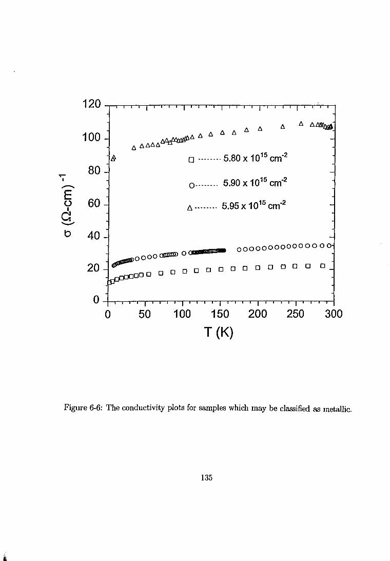
T"" I
.....-....
100
80
5 60 I
a .....,_;
b 40
20
0
o-------· 5.90 x 1015 cm-2
6 -------· 5.95 x 1015 cm-2
~ooooamm:> QliD •;mil- OOOOOOOOOOOOO 0 0
~ oooooooooo oooo o o o o
50 100 150 200
T (K)
250 300
Figure 6-6: The conductivity plots for samples which may be classified as metallic.
135

Chapter 7
Electrical conductivity results of
boron-ion implanted diamond
7.1 Introduction
The electrical conductivity results, measured in the temperature range 1.5-773 K,
are presented in this chapter. In order to gain a better understanding of the transport
phenomena in this system, I have employed a number of theoretical procedures to ma
nipulate and interpret the experimental data. This chapter has been divided into four
main sections. Section 7.2 presents the electrical conductivity results on the insulating
side of the transition. Section 7.3 summarizes the results in the metallic regime, while
section 7.4 describes the conductivity data for samples located close to the M-I transi
tion. Section 7.5 reports on the high-temperature (300-773 K) results carried out on both
insulating and metallic samples.
136

7. 2 Insulating samples
7.2.1 Motivation
The electrical conductivity measurements on the insulating side of the transition have
been motivated by three objectives. The first objective is to determine the highest value
of the boron concentration at which samples still show a characteristic behaviour of
insulating materials. We expect that beyond this limit the relation a ---+ 0 as T ---+ 0 will
be invalid when the transition is approached from below.
The second objective is to identify clearly the transport mechanisms in the boron
ion implanted conducting surface layers as the temperature of the samples is lowered.
This involves a careful determination of the hopping exponent m in the VRH relation,
a(T) = a 0 exp [- (To/T)m]. As reported in chapter 2, the theoretically determined val
ues for m are 1/4 (Mott VRH law with a constant and non-vanishing DOS), and 1/2
(ES VRH law with parabolic-shaped DOS at the Fermi energy). From these transport
properties, the behaviour of the single-particle DOS near the Fermi energy can be estab
lished. Another phenomenon that we have probed in this system is the occurrence of the
electrical conductivity crossover from Mott to ES VRH behaviour. This phenomenon has
widely been studied but observed in only a few doped semiconductors[168, 174, 175].
The third objective is to determine whether the system undergoes a dimensionality
crossover as the temperature of the samples is decreased. To do this, we compare the
ratio of Rhop tot, the thickness of the implanted layer, which is obtained from the SIMS
profile, and is also estimated from the TRIM92 computer simulation program. An average
thickness of the boron-ion implanted layer according to TRIM92 is 0.21 J.Lm, while the
SIMS profile measures this thickness to be 0.25 p,m.
Fig. 7-1 shows plots of resistance against temperature for a number of insulating
137
l
boron-ion implanted diamond specimens measured in the range of temperature 1.5-300
K. The plots follow a general resistance (resistivity) relation, R(T) = Ro exp [(T0 /T)m].
The parameters R0 , To and m have been determined using several methods. One of
the methods used is the Minuit software package least squares fitting procedure. In
this program, parameters were allowed to vary within specified bounds or were fixed
to theoretically predicted values. The characteristic temperature values, including error
estimates, obtained using the Minuit program are listed in table 7.1.
The standard procedure widely used by various researchers in this field[176] to dis
tinguish between the Matt and the ES VRH relations is to plot p(T) (or a(T)) versus
r-1/ 4 and r-112 , respectively. These plots are shown in Fig. 7-2(a,b), covering a wide
range of insulating samples. From these plots curves which show some linearity with the
experimental data are selected and the least squares regression lines fitted to them. Fig.
7-3 shows a plot of the least-squares fit for one of the insulating samples (AB27) together
with the experimental points. The fit is excellent over the range shown, with m rv 0.5.
We have, however, noted that, as the M-1 transition is approached, the least squares
fitting method yields poor values for the fitting variables. Hill(74] and other authors[104]
have noted that quantities extracted using this fitting procedure are unreliable, because
fittings are usually confined to a small segment of R-T experimental data. If one slightly
increases the previous R - T data range for fitting, one always obtains different values
for the fitting variables. The procedure used by Hill(74] and Hill and Jonscher[75], and
later Zabrodskii and Zinov'eva[76], will be presented in the discussion chapter (chapter
8).
138

1011
1010
109
108 ,-.....
c 107 _,.......
~
•106
105
104
103
0
0
0 0
50
0 oo
0 Do
100 150 200 250 300
T (K)
Figure 7-1: The resistance against temperature for a number of boron-ion implanted type Ila diamond specimens.
139

Sample Symbol TM (K) TEs (K)±("" 5%)
Name x104
AB21 0 274±5.5 6291
AB24 0 320±48 7183
AB27 !:::. 49±5.8 2238
AB30 <> 65 ±5.2 1738
AB33 * 1.28 ±0.12 2020
AB36 + 10.5± 0.9 1043
AB39 X 1.03 ±0.07 1020
AB42 • 0.92±0.10 185
AB45 • 8.34± 1.2 262
AB48 .A 2.05±0.2 102
Table 7.1: The Minuit least squares fitting procedure was used to determine values for the characteristic temperatures in the Mott and the ES VRH regimes. The uncertainty in the characteristic temperatures were estimated by fitting the regression lines over various temperature regions in which the Mott and the ES laws apply. The non-monotonic decrease in TM and TEs may be an indication of the unreliability of this method
140

~
c _....
0::
-c _.... 0::
1011
1010
109
108
107
106
105
104
103
0.2
1011 1010
109
108
107
106
105
104
103
0.0 0.1
0.4
0 0
00 • 0 • +
0 • +
•
• + • •• • ++ • • A A , .. . . .
++ ••• + • rt• •••• •• . . . "
•• • A A o AA •
AA • A ••• .....
0.6 0.8
r114 (K-1'4)
+ + •
• A
0.2 0.3 0.4 0.5 0.6
r1'2 (K-112)
0 ------------ 2.1
0 ------------ 2.4
ll ------------ 2. 7
------------ 3.0
* ------------ 3.3
+ ------------ 3.6
X ......................... 3.9
• ......................... 4.2
• .. ........................ 4.5
4 ....................... 4.8
• .. ...................... 5.1
Figure 7-2: Resistance of eleven insulating diamond specimens plotted as a function of r-m (K-m) {where m = 1/4 and 1/2) on a semilogarithmic scale.
141

8.0
............... "<;f"
I
0 or-
6.0 X ....._.... "r"
I ..............
E u 4.0 I c ....._....
b
2.0
0 10 20 30 40 50
T (K)
Figure 7-3: u vs. T for sample AB27. A solid line through the experimental data represents a fit to the conductivity expression: u(T) = CJ0 exp [- (To/T)m] where m rv 0.5.
142

7.3 Metallic Samples
7.3.1 Motivation
The objective of our investigation has been two-fold. Firstly, to determine a lower con
ductivity value on the a - T experimental data below which the condition, a(O) ----+
A as T ----+ 0, where A is a finite positive value, is invalid.
The second objective is to study the dominant transport mechanisms in this system,
particularly at low temperatures. This means fitting our experimental data, collected in
the vicinity of the transition, to the conductivity expression given later by Eq. (7.1) to
determine a(O) and Z. Therefore, obtaining a correct expression of a(T) is important for
a reliable determination for a(O) since a(O) defines the position of the M-I transition.
Recall from chapter 2 that samples with a(O) = 0 are classified as insulating, while
samples with a(O) > 0 are metallic.
Fig. 7-4 shows plots of a(T) as a function of T(K) for some metallic samples. We
have carried out the conductivity measurements in the absence and in the presence of
a magnetic field on some metallic samples. The results for samples AB81 and AB84,
annealed at 1873 K (1600 °C) and 1973 K( 1700 oc), are shown in Fig. 7-5 and Fig. 7-6,
respectively. It is difficult to clearly resolve the curves for conductivities measured with
and without a B-field. I therefore decided to ignore the weak inelastic scattering term,
STPI2 , in the fitting function,
a(T) = a(O) + CTz , (7.1)
for two reasons: (i) the contribution of a B-field, which was set to a maximum of B
= 1 T, is insignificant, and (ii) we could not reach temperatures below 1.5 K due to the
constraints of our cryogenic system. This means that we extrapolated our conductivity
results from 1.5 K to 0 K to determine a(O). The dropped inelastic term would have
143

otherwise served as just another fitting parameter which would have improved the fit,
but would have been of questionable physical significance for our system. Recently,
Aronzon[177] suggested that I try measuring our samples in the presence of a weak field
of strength 0.1-0.5 T to see if I could pick up effects due to weak localization. The
preliminary results obtained here did not yield the desired effect, but this study may
be followed up after the completion of this thesis. The prefactor C in Eq. (7.1) forms
part of the electron-electron interaction term (second term) and may change sign when
the M-I transition is crossed, with the conductivity exponent Z expected to take values
between 0.5 to 1.0. It has been noted that a sign change of C can also occur for weakly
insulating systems which are located close to the M-I transition[106, 107].
Parameters obtained from Eq. (7.1) are presented in table 7.2. The focus is on the
electrical conductivity carried out below 50 K. Fig. 7-5 shows a plot of ~(T) against
T for a sample close to the M-I transition.
7.4 Conduction near the M-I transition
7 .4.1 Motivation
The main objective is to locate precisely where the M-I transition in boron-ion implanted
surface layers in single crystal type Ila diamond occurs.
A secondary motive is to test the applicability of several theories or models which
attempt to describe the transport properties at and quite near the transition.
For a system very close to the transition, an exponent of 1/3 in the electron-electron
interaction term gives a better fit than 1/2. This is shown in Fig. 7-7 for a tempera
ture range of 1.5-30 K. The theoretical justification for an exponent of 1/3 is given by
144

100
80 ••• • • • • • • • •
••••• ••••
oor- - • • • • 1
...............
E () 60
I c --b 40
20 ... , ..
0 10 20 30 40 50
T (K)
Figure 7-4: The electrical conductivity for some of the metallic samples plotted as a function ofT. Samples have been annealed isochronally {10 minutes) at various temperatures ranging from 1200 octo 1700 °C. Symbols shown represent: •-sample AB84 (1700 oc anneal); £-AB81 (1700 oc anneal); •-AB78 (1700 oc anneal); .6-AB81 (1200 oc anneal) +-AB78 {1200 oc anneal). All samples have been annealed for 10 minutes.
145

,..... I ,.-...
E 0
c .._. b
12~----------------------------------------~
10
8
6
4
2
0
-2
n=4.1 x 1 021 cm-3
cr = cr(O) + BT1t3
12
10
"""' 8
I -E 6 "" cr = cr(O) + BT1t2 0
c - 4 b
.2
0
0 5 10 15 20 25 30 T(K)
0 5 10 15 20 25 30
T(K)
Figure 7-5: Electrical conductivity vs. T for sample AB81. This sample has been annealed at 1700 oc.
146

28
or-26 I
............
E (.) I c ....._., 24
b
22
0
n=3.9x1 021 cm-3
0
"' cr(T )=q(O) + BT112
5 10 15
T (K)
20 25 30
Figure 7-6: Electrical conductivity vs. T for sample AB84. This sample has been annealed
at 1700 °C.
147

Sample Anneal T(°C) cr(O) c z AB78 1200 0.44 .95 .72
1200 3.18 .33 .94 1200 6.25 .04 1.34 500 3.58 1.59 .66 500 1.32 0.90 .72 500 1.53 1.74 0.5 1700 0.44 2.43 0.43
AB81 1200 3.81 .20 1.02 500 3.66 .35 .95 500 3.52 .32 .93 1300 5.62 2.06 .64 1400 11.07 .24 1.05 1600 15.56 0.08 .74 1700 22.61 0.77 0.64
AB84 1700 73.12 0.52 1.04
Conductivity exponent Z fixed to a 0.5 + Sample Anneal TC0C) cr(O) c z
AB78anl6 1700 5.62 2.06 0.5
AB81anl1 1200 0.53 2.14 0.5 AB81anl8 1300 1.85 4.04 0.5 AB81anl9 1400 9.07 1.95 0.5
Table 7.2: Variables of boron-ion implanted diamond obtained from the metallic expression are presented in this table.
148
Maliepaard et al.[108] and by a number of authors using different approaches(115]. This
exponent has recently been found in other neutron doped systems[16, 105, 178]. Recent
studies by Castner[92] re-emphasize the 'universality class' of Z = 1/2 for systems close
to the M-I transition.
7.5 The derivative method
The derivative method has been used to characterize the transport properties of our
samples. The basic tenets of this method and its application to disordered systems are
presented in chapters 2 and 8. Fig. 7-8 shows a typical trend of some W- T plots for
one of the samples (AB81) in the vicinity of the M-I transition. The sample has been
annealed at various temperatures (from 1200 oc to 1700 °C) for ten minutes.
7.6 High-temperature measurements
7.6.1 Motivation
The principal objectives are (i) to extend transport studies to systems which show VRH
behaviour at low temperatures, and (ii) to measure activation energies and compare them
with activation energies which were obtained at low temperatures.
Electrical conductivity measurements on two samples, one highly insulating and the
other just metallic, have been carried out in the temperature range 300-773 K. Fig. 7-9
shows R plotted against 1/T for sample B84. The insert shows the same experimental
data plotted against r-1/ 4 to determine whether the Mott VRH behaviour applies in
this sample at high-temperatures. We show only the results for insulating samples after
encountering electrical contact problems at high temperatures in the case of metallic
149

90 I .J.A~ (a) - ~ AA.J.A -
..... I - 60- -E 0
c --~ 30- -----= - - - ----b -. ...--- - -
0 I . 0 1 2 3
T113 (K1/3}
1.0 1.8 2.7 3.5 4.4 5.2 10
9 (b) .....
I 8 -E 7 0
c 6 --1-5 -b
4
3 1 2 3
T113 (K1'3)
Figure 7-8: Temperature-dependent electrical conductivity vs. T for samples AB78, AB81 and AB84. A closer inspection of the plots reveals that u(T) vs. T 113 gives a better fit to the experimental data than u(T) vs. r-112
• Plotted here are samples annealed at 1700 oc for 10 minutes. Sample AB84 is shown in Fig. 7-B(b).
150

0.8 •
0
•
0.6
0.4
0.2
0 20 40
•
500°C
( .. • • •
1200 oc ( 0 0
60
T (K)
•
• • • .. •• • • • • • • • • • .. •
• 0
{ 1500 oc
££ ................... £ ~£.c-·----
• • •
80 100
Figure 7-9: Plots of activation energy w = a In (J I In T against T. This sample, AB81, is close to the M-I transition. According to the derivative method, sample AB81 is weakly insulating. One of the curves fitted with a solid line has been annealed at 1700 oc, which is the highest temperature at which we can safely anneal our samples. The annealing temperatures for these samples are shown in the figure. The duration of the anneal for all samples was set to 10 minutes. 151
samples. Above ""' 400 K the behaviour changes from hopping conduction to activated
carrier transport involving holes in the valence band.
152

Ol 0
2.64
2.63
2.61
2.60
1.0
T(K)
• • • .... . . •
• • • • •••••••• • •
·-·· , ..... , •
•• .. , tl -a
~
~
• ~
0> 0
•
1.5
2. 65 -,-r1rTTlr-rr"J"TT"'TTTT"TTTTTTT'TITTITT"T'"r-r-r-",........,
2.64
2.63
2.62
2.61
2.60
2.59 0.18 0.19 0.20 0.21 0.22 0.23 0.24 0.25
(T(K)) -1/4
2.0 2.5 3.0
1 000/(T(K))
3.5
Figure 7-10: Plots of R(T) vs. r-m for sample AB84 measured in the temperature range 300-773 K. The insert shows the same experimental data plotted against r-1
/4
to check whether Mott VRH conduction applies in this temperature range.
153

Chapter 8
Discussion of the electrical
conductivity results for boron-ion
implanted type lla diamond
8.1 Introduction
This chapter discusses the experimental results presented in chapter 7. The chapter
has been broken up into three main sections, each focusing on broader aspects of the data
analysis. In section 8.2 I discuss the electrical conductivity results on the insulating side
of the transition using the current variable-range hopping theories. Section 8.3 is devoted
to results obtained on samples located in the metallic domain. The range and validity
of the fitting functions used to analyze the data are discussed. Section 8.4 interprets
the results in the vicinity of the metal-insulator (M-I) transition in the framework of
the scaling theory of localization. Compensation of boron impurity centres by vacancy
related defects is discussed in section 8.5.
154
8.2 Insulating samples
This is the regime where most of the experimental work has been done. It will therefore
be the most elaborate section. When this study was initiated, I had four virgin, optically
transparent and well polished samples with which to work. As described in chapter 4,
the letter A denotes the sample, B stands for the dopant ion (in this case boron), and
the number represents the implanted dose ( x 1015 cm-2). For example, if sample A is
implanted with a dose fluence, or to a total dose fluence, of 5 x 1015 cm-2, it will be
designated as AB5.
For convenience, I have converted the boron-ion dose levels to concentrations in some
tables where the electrical conductivity quantities are presented. I decided to stick to
one nomenclature in referring to my samples, and this involves the use of dose levels.
Where necessary I have written down the concentration in brackets, particularly in later
sections where I discuss the transport properties in the vicinity of the M-I transition.
I began monitoring the electrical conductivity behaviour for sample A after it had
been implanted progressively, using an incremental dose of 3.0 x 1015 cm-2, for the
seventh time. This means that the experimental data for conductivity as a function of
temperature were first collected when the implanted dose had reached a level of 21 x
1015 cm-2 (sample labelled as AB21). Samples B, C and D have been implanted slightly
differently to sample A, and annealed differently. We implanted these samples with a
total dose of 5.0 x 1015 cm-2, which is just below the critical threshold beyond which
the implanted layer would undergo irreversible structural changes with the appearance
of graphitic regions. Unlike sample A which has been annealed initially at 1200 oc for
155

a standard duration of 10 minutes until a total dose of 78 x 1015 cm-2 was implanted,
samples B to D have been annealed at 500 oc (for at least 120 minutes), 700 oc (30
minutes), 900 oc (30 minutes), 1200 oc (10-30 minutes) and up to 1700 oc (10 minutes).
After every implantation-annealing cycle, these samples were repolished immediately
after I had measured their electrical conductivities as a function of temperature. It was
not until the initial stage of the project had been completed that we decided not to
repolish them, but to carry on implanting them incrementally with the same boron-ion
dose of 5.0 x 1015 cm-2 , and to anneal them at 1200 oc (for 30 minutes) and 1700 oc (for 10 minutes). Conductivity measurements were performed in between the anneals. A
list of the implants for these samples is given in chapter 4.
8.2.1 Activation conduction mechanism
An alternative way of presenting the data shown in Fig. 7-1, is to plot R vs. 1/T. This
representation is motivated by the expectation that the data would be described by an
activated conduction mechanism. The activation energy for such a transport process
would then be given by the slope of the straight line on the graph. Typical studies of
the M-I transition have examined R(T) in samples that are approaching the transition
from the insulating side and determined the value of nc by the disappearance of a low
temperature activation energy cJ[179, 180, 181]. In the regime where activated conduction
takes place
(8.1)
where Po is the temperature-independent prefactor, EA is the activation energy and kB
is Boltzmann's constant. Taking natural logs on both sides of Eq. (8.1) yields
(8.2)
156

and EA can be obtained from the slope using Eq. (8.2), as
5 (~lnR) EA = 8.614 X 10- X ~1/T eV (8.3)
Figs. 8-1 and 8-2 show plots of R against 1/T for a number of samples measured in
the temperature range 1.5-300 K and 300-773 K. It is difficult to see from these figures
whether our system shows transport properties associated with the activated conduction
process or not, unless one selects a small segment of R - T data for analysis. Table 8.1
lists values for some important quantities related to electrical conductivity.
8.2.2 The derivative method for the insulating materials
Before discussing the experimental results pertinent to this section, I wish to make the
reader aware that the plots made in Figs. 8-3-8-5 have been generated using two different
methods. I have put the figures together for the reader to note the consistency of the
two methods. These methods will, however, be discussed separately. We begin with the
"w-derivative" method.
Recall from chapter 2 that the temperature dependence of the electrical conductivity
of an Anderson-disordered insulator at low temperatures, follows the general variable
range hopping (VRH) law,
Substituting Eq. (8.4) into Eq. (8.5) shown below (defined in chapter 2) gives
w olna _Tolna -----oinT 8T (mT;)T-m
157
(8.4)
(8.5)
(8.6)

1011
1010 0 0 00
109 00
00 o<>
108 • - +
a 107 + ......._ + X
+
0:: 106 X •
X • • 105
104
103
0 20 40 60 80 100 120
1 000/ (T(K))
107
§: 105 k300€~~~~~~:.i ~
103 ;-.. ~~~~~~~~~
3.5 4.0 4.5 5.0
1 000/ (T(K))
Figure 8-1: Plots of R vs. 1/T for a number of insulating samples. Only the data above 400 K may be used for the calculation of the activation energy, EA.
158
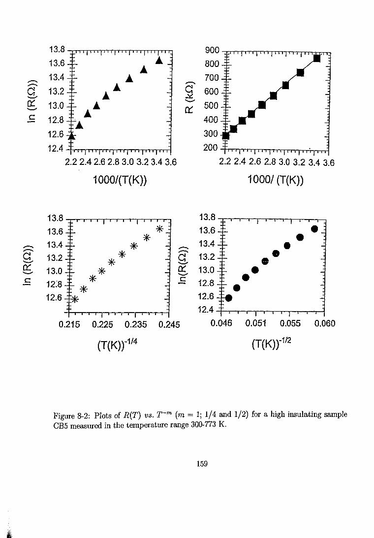
--a '-"' 0::: ...........
c -
_...._ _...._ c ............. 0:: .............
c
13.8
13.6
13.4
13.2
13.0
12.8
12.6
12.4
13.8
13.6 13.4 13.2 13.0 12~8
12.6
... ...
2.2 2.4 2.6 2.8 3.0 3.2 3.4 3.6
1 000/(T(K))
-900~~~rrn~~~~~
BOO
700
s 600 '-"' cr: 500
_..., _..., c '-"' 0:: '-"' c
400
300
200~~~~~~~~
13.8
13.6 13.4 13.2 13.0 12.8 12.6
12.4
2.2 2.4 2.6 2.8 3.0 3.2 3.4 3.6
1 000/ (T(K))
• • • • • • • • 0.215 0.225 0.235 0.245 0.046 0.051 0.055 0.060
{T(K)f1t4 {T{K)f1t2
Figure 8-2: Plots of R(T) vs. r-m (m = 1; 1/4 and 1/2) for a high insulating sample CB5 measured in the temperature range 300-773 K.
159

Sample
Name
AB21
AB24
AB27
AB30
AB33
AB36
AB39
AB42
AB45
AB48
HighT Data Low T data
Dose Symbol TM (K) Rhop,M/e TEs (K) Rhop,Es/e a (108 m-1) e (run)
(x1015 cm-2) x104
21 . 0 274 15.3/T114 6291 6.34/T112 3.02 4
24 0 320 15.9/T114 7183 21.19/T112 3.45 3
27 b. 49 9.92/T114 2238 11.83/T112 1.07 9
30 0 65 10.65/T114 1738 10.42/T112 0.83 12
33 * 1.28 4.03/T114 2020 11.24/T112 0.97 10
36 + 10.5 6.75/T114 1043 8.07fT112 0.50 20
39 X 1.03 3.78/T114 1020 7.98/T112 0.49 20
42 • 0.92 3.67/T114 185 3.40fT112 0.089 113
45 • 8.34 6.37/T114 262 4.05/T112 0.013 80
48 j, 2.05 4.49/T114 102 2.53/T112 0.049 204
Table 8.1: Values of variables determined using electrical conductivity expressions are described in the text. The error estimates for TM and TEs were given in table 7.1.
160

Taking the logarithm on both sides transforms Eq. (8.5) into a straight line graph of the
form,
logW = -mlogT +log(mT:) (8.7)
Consider Eq.(8.5). For insulating samples, W is always positive and it diverges as T ~
0. This behaviour is supported by plots shown in Fig. 8-3 and Fig. 8-4, and has been
observed widely by various authors[174]. The applicability and validity of the derivative
method have been extended even to samples that exhibit finite conductivities at T = 0
K, as shown by plots in Fig. 8-5. Samples shown in Fig. 8-5 cannot be interpreted
using Eq. (8.4) even though they are classified as insulating by the derivative method.
It is interesting to note that a finite u(O), according to the derivative method, does not
necessarily mean the exhibition of metallic behaviour[13]. Later in the chapter it is shown
that the derivative method does not work well for n ~ nc.
The advantage of the "w-derivative" method is that one does not have to assume
any parameter dependence beforehand because the linear region of log W versus log T,
defines the region where VRH occurs. The hopping exponent m can be obtained directly
from the slope, using the least-squares fitting procedure. Once m is known, then the
characteristic temperature T0 can be calculated ~om Eq. (8.7) as
( 10Yint) l/m
To= -m
(8.8)
where Yint is an intercept read from theW ordinate. Variables obtained using the deriv
ative method are summarized in table 8.1. Further details of the derivative method can
be found in recent articles by Rosenbaum et al.[28, 29, 106, 174].
There is, however, a disadvantage associated with the "w-derivative" method. It is
very sensitive to any variation of the experimental data, and even small local fluctuations
161

in the data become amplified. To overcome this draw-back two methods have been
suggested. One method involves fitting a fifth-order polynomial through the experimental
data points and then extracting pertinent information from the fitted curve. This method
was used by Buraschi et al.[184]. Another method, which I have used throughout(174,
185], is to group the adjacent data points into small units and then calculate the averages
of Rand T per group. A unit may be made up of 4 data consecutive points or more,
depending on the magnitude of the scatter in the experimental data set(174, 186]. Our
data did not show much scatter, so only two consecutive data points were used to work
out the averages.
A method analogous to that used by Hi11(74] above has been suggested by White and
McLachlan(187], following the earlier work of Davies et al.(188], in which they showed(187]
that
olng oinT = -mln(g)- mln(Ro) (8.9)
in the regime where the VRH relation is valid. This method has been included for com
pleteness, and has been captured in Figs. 8-3(b )-8-5(b) which show a series of samples
located in the insulating regime. The scatter in the experimental data becomes pro
nounced when the M-I transition is approached from below. In order to control this
scatter, some shape-preserving cubic splines such as AKIMA(189] have been used. I have
found this method not any better than that of Hi11(74] and Zabrodskii-Zinov'eva(76],
particularly for samples that are in the vicinity of the M-I transition.
8.2.3 Variable-range hopping conduction
Although hopping conduction in heavily doped and Anderson disordered semiconduc-
162

C) 0
...-.. r-......_...
c 32 ...-.. C) ......_... c -""0
0.6
0.2
0.0
'\. '\.
I'' ~
slope =-1/2 ,
0.5 1.0
Tcross = 80 K
1.5 2.0 2.5
log {T(K))
7 \. DG ~
6 \. qpe. X
\. 0 ~t. t. \.
5 '\. '\.
\. 0
4 /' 3
slope= -1/2
2
1 -24 -20 -16 -12 -8
In (g)
Figure 8-3: The derivative method and the White-MacLachlan method were used to generate these plots in an effort to determine the hopping exponent m. Samples plotted here lie in the boron-ion concentration range: 1.0- 1.9 x 1021 cm-3 • ·
163

0.6
0.5 _..._
0.4 _..._ r-.............. s 0.3 ..............
0> 0.2 0
0.1
0.0 0.8 1.2 1.6 2.0 2.4
log (T(K))
5 • • A
0 _..._ J- 4
1!1 • ..............
c 0 • o.
32 3 'b o. fllo
............. • 0>
..............
c 2 -"'C
1 -18 -16 -14 -12 -10 -8
din (g)
Figure 8-4: The derivative method and the White-MacLachlan method used to generate plots shown in an effort to determine the hopping exponent m. Samples lie in the boronion concentration range: 2.0- 3.0 x 1021 cm-3
. The fitted slopes close to the theoretical hopping exponent of 1/2 are shown in the plots.
164

0.2
0
0.0 0 -- 0 --r ............
$ -0.2 ............
0> 0
-0.4 slope=-1/2
-0.6 0.5 1.0 1.5 2.0 2.5
log {T(K))
1.6 ++
-- slope=-1/2 + +
r +. ............ 1.2 +
c: 'U ----0> 0.8 ............ c: 'U
0.4 -11 -10 -9 -8 -7
In (g)
Figure 8-5: The derivative method and the White-MacLachlan method used to determine the hopping exponent m. Sample AB78 (n ~ 4.0 x 1021 cm-3
) is shown. Solid lines shown in the plots correspond to theoretical slopes of -1/3 and -1/2. From the plots, a slope of -1/3 gives a better fit to the data compared to a slope of -1/2. The annealing temperatures for this sample are shown in the table alongside this figure.
165

tors has been studied intensively over many years[104, 190], a transition from Mott to
ES VRH has been observed experimentally only in relatively few cases[27, 168, 174, 191,
192, 193]. In most of these cases, the electrical conductivity crossover occurs at very low
temperatures, in some at T :::; 5 K[194]. The advantage in our system is that the VRH
conductivity crossover is observed at temperatures around 100 K and depends on n (see
Fig. 8-3(a)), where n is the boron-ion concentration.
The conductivity data shown in Fig. 8-3(a,b) are clearly governed by the Mott VRH
relation[8], a(T) = a 0 exp [- (TM/T/14], at temperatures above 100 K. The linearity
expressed by the data shown in Fig. 7-2 is taken to be indicative of long-range hopping
conduction with a constant density of states at the Fermi energy, with the effective tem
perature TM =!3M/ (kBeNa(EF)). There exists, however, a considerable discrepancy
as regards the values of the coefficient /3M, which, in turn, has a sensitive bearing on
TM. Mott has provided the following values for !3M : 1.5[195] and 24/7r = 7.6[196], while
Castner has used 18.1[104]. Skal and Skhlovskii[197] estimated !3M to be 21.1, which is
smaller than a value suggested by Ortuno and Pollak[198] of !3M= 27. The controversy
surrounding the f3M value remains unresolved, but many authors have settled for Cast
ner's value of 18. Further reading on the controversy concerning !3M can be found in a
recent article by Rosenbaum et al.[27].
As the temperature of the disordered insulator system is lowered (below 100 K), ef
fects due to long-range electron-electron interactions start to dominate, giving rise to a
depletion in the density of states at the Fermi energy. Electrical conductivity for samples
which obey the relation a(T) = a0 exp [- (TEs/T) 112] , where the characteristic tem
perature TEs = e2f3Es/ (kBE~), with f3Es taking values of 2.8(23], 0.57(170], or 7.27[27],
is interpreted in terms of the ES VRH mechanism within the Coulomb gap ( Cg). The
theory of the Cg is presented in chapter 2.
166

It is apparent from the derivative method plots shown in Figs. 8-3-8-5 that no single
value for the hopping exponent can adequately describe the type of VRH conduction
taking place over a wide temperature interval. There exists a conductivity crossover
between the Mott VRH (m = 1/4) and the ES VRH (m = 1/2) as the temperatures of
the samples are lowered. The conductivity crossover (see Fig.8-3), is around 100 K. It is
difficult though to determine precisely by means of this method the R - T cutoff point
beyond which either of the two VRH conduction mechanisms ceases to apply.
We have found, by comparison with other methods such as the White and MacLach
lan method[187], the derivative method to be the most sensitive and reliable in probing
the transport nature of doped materials.
8.2.4 The optimum hopping distance and tunneling exponent
The amount of disorder and the material temperature determine the distance over which
a carrier will hop[44]. In this section, we examine the transport properties of OC:B
(boron-ion implanted diamond) in the VRH conduction regime further. We also calculate
some values for model parameters which are important in the VRH regime, and study
conditions to which the current VRH theories apply in our system.
Important parameters in the VRH conduction theory are the ratio of the mean hop
ping distance to the localization length (radius), Rhop/e, and the mean hopping energy
difference between the localized impurity sites, tl.hop. Expressions for these quantities in
the Mott VRH conduction regime (with fJM chosen to be 18) are [104, 174]
Rhop,M(T) = ~ (TM) 114
e s r (8.10)
167

and
(8.11)
In the ES VRH regime (with f3Es = 7.27), we have
Rhop,Es(T) = ~ (TEs) 112
~ 4 T (8.12)
and
(8.13)
The validity of both the Mott and ES VRH models depends on the condition, Rhop(T) 1 ~ >
1. Re-examining the sample parameters listed in tables 8.1-8.3, the condition, Rhop(T)I~
> 1, may well be satisfied at lowest temperatures, say at temperatures below 5 K. This
condition holds for both the Mott VRH and the ES VRH theories.
We consider the situation in the ES VRH conduction regime. In addition to the
condition that Rhop(T)/~ > 1, there is another important condition which has to be met.
The temperature-dependent optimum hop energy of the variable-range hopping process
llhop,ES must satisfy llhop,ES > kBT for hopping to take place within the Cg. In other
words, TEs must always be greater than the measured sample temperature for one to
invoke the ES VRH law.
The temperature-dependent tunneling exponent in the ES regime is given by (170]
= kBTEs (1r )1/3 a 10.5 gES (8.14)
where gEs = (387r2 E~E~) I (25e6) = 1.55 x 1085 J-1m-3 for Er = 5.7 (diamond). Substi
tuting values for the standard constants in Eq. (8.14) yields (in the case of diamond) a
simpler expression with which to work, viz.
168

(8.15)
We can then express the maximum hopping distance in terms of TEs (cf. Eq.(8.14)) as
- 6 1~ Rhop,Es = 5.2 x w- (T TEsr (m) (8.16)
The tunneling exponent decreases with increasing concentration as nc is approached from
the insulating side. Table 8.1 shows entries for Rhop(T)/€ as a function of temperature,
and some other related quantities.
We can now determine how Rhop(T) compares to t by using variables obtained for
sample AB21. We calculated TEs = 6291 K for sample AB21. At T = 5 K, Rhop,ES ~ 29
nm. According to SIMS profile (see chapter 4), t is measured to be 250 nm. This means
that Rhop(T) < t and hence our system is 3-dimensional. We expect Rhop(T) to grow as
the sample temperature is lowered, and for doses close to the transition (with TEs very
small) we may have Rhop(T) ~ t. A dimensional crossover in systems of this sort has
been observed before[173].
We have much confidence in quantities extracted from the ES VRH regime, compared
to those obtained in the Mott VRH regime due to the scatter in the W - T data sets for
T ~ 100 K. I have estimated the uncertainty values for TM and TEs in table 7.1.
8.2.5 A crossover between Mott andES variable-range hopping
Castner[104] has recently made some interesting theoretical predictions for insulating
samples located not too far away from the M-I transition, but which still show a conduc
tivity crossover from the Mott toES VRH laws as the temperature is lowered. Castner's
predictions involve the ratios,
169

and
TM 18 (47r) -= TEs !3Es
TEs =!3Es (47r)l/2 Tc9
(8.17)
(8.18)
(8.19)
The quantity Tc9 is referred to as the 'Coulomb gap' temperature. It is the temperature
below which the effect of a Cg on the hopping process is evident. Just beyond Tc9
, the
Mott VRH becomes a dominant transport process. Eq. (8.18) does not depend on
f3Es, rendering this equation very useful for estimating Tc9 without having to adjust any
parameters. The disadvantage though, in my case, and for other authors as well(174],
is that TM cannot be determined to a high degree of accuracy, compared toTEs, due
to scatter in the experimental data. Eqs. (8.17) and (8.19) contain the coefficient f3Es,
which depends upon the compensation ratio k = NA/Nv, where NA and Nv are the
acceptor and the donor concentrations, respectively. It is difficult to determine the value
for f3Es in OC:B system since it was not compensated by any extrinsic defect atoms. The
only compensation effect we have is due to vacancy-related intrinsic defects.
A number of theoretical values for f3Es (viz. f3Es = 7.27, 2.8 and 0.57) have been
reported in the literature as I mentioned earlier. We have used these values in Eqs.(8.17)
(8.19) to estimate Tc9 for the OC:B system. Such a procedure also affords one the ability
to probe the consistency in the VRH laws. The Tc9 values are summarized in table 8.2.
By using values of TM, TEs and Tc9 , shown in tables 8.1 to 8.2, respectively, we can
estimate f3Es in OC:B system to be~ 0.57. This value was predicted by Adkins(l70]. I
cannot attach any physical significance to this f3Es value, but it appears to be system
dependent(27].
170

Considering our inability to determine the Mott characteristic temperature with much
accuracy, our results still seem quite consistent with the experimental findings of Zhang
et al.[168] on the relationship, TEs ex: (TM )213 . This is shown in Fig. 8-6.
8.2.6 Coulomb gap and the crossover temperature
In this section we discuss the importance of the Coulomb gap in our system and its size
in the light of our experimental results.
The size of a Coulomb gap /).c9 has been determined independently by several
authors[38, 17 4, 199] to be
/:). = ..!!_N(E )1/2 = k ES 3 (T3 )112
Cg E3/2 F B TM (8.20)
A number of equations leading to the calculation of the size of a Cg are presented below
using the existing VRH expressions. From the Tc9 expressions (Eqs. (8.18) and (8.19)),
we can write l:::..c9 as
(8.21)
and
(8.22)
The electrical conductivity crossover, from the non-electron interaction Mott VRH regime
into a strong long-range electron-electron correlation regime of ES, is expected to occur
when the mean hopping energies, /).hop,M and l:::..hop,ES, are of comparable magnitude.
Combining Eq. (8.11) and Eq. (8.13) defines the crossover temperature as[104, 174]
Tcr = 16 (~:) (8.23)
Using Eq.(8.23), we can then express /).c9 as
171
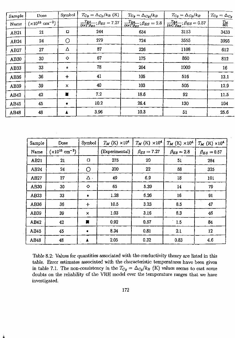
Sample
Name
AB21
AB24
AB27
AB30
AB33
AB36
AB39
AB42
AB45
AB48
Dose Symbol Tc9 = .D.c9 /kn (K) Tc9 = .D.c9 /kn Tc9 = .D.c9 /kn Tcg = .D.c9
(x1015 cm-2 ) (4~~PEs; fJEs = 7.27 T~s . {3 - 2 8 (4~~PEs; fJEs = 0.57 2M (47r):ri3R.<: I ES - . 801
21 0 244 634 3113 3433
24 0 279 724 3555 3995
27 l:l 87 226 1108 612
30 0 67 175 860 812
33 * 78 204 1000 16
36 + 41 105 516 13.1
39 X 40 103 505 12.9
42 • 7.2 18.6 92 11.5
45 • 10.2 26.4 130 104
48 A 3.96 10.3 51 25.6 --
Sample Dose Symbol TM (K) x104 T:v (K) x 104 TM (K) xl04 TM (K). xl04
Name (x1015 cm-2) (Experimental) .Oss = 7.27 f3Es = 2.8 f3Es = 0.57
AB21 21 0 275 20 51 284
AB24 24 0 320 22 58 325
AB27 27 "f:l. 49 6.9 18 101
AB30 30 0 65 5.39 14 79 .
AB33 33 * 1.28 6.26 16 91
AB36 36 + 10.5 3.23 8.5 47
AB39 39 X 1.03 3.16 8.3 46
AB42 42 • 0.92 0.57 1.5 84
AB45 45 • 8.34 0.81 2.1 12
AB48 48 A 2.05 0.32 0.83 4.6
Table 8.2: Values for quantities associated with the conductivity theory are listed in this table. Error estimates associated with the characteristic temperatures have been given in table 7.1. The non-consistency in the Tc9 = D.c9/kB (K) values seems to cast some doubts on the reliability of the VRH model over the temperature ranges that we have investigated.
172

9~---------------------------.
7
("')
0 ~
X .......- 5 ~ __,
en w r--
3
1~~~~~~~~~~ •. ~.~~~~~
0.0 0.8 1 .6 2.4
Figure 8-6: This plot demonstrates the relationship between the Mott and ES characteristic temperatures in the VRH regime.
173

(8.24)
Four expressions for D..c9 have been written down, and I have checked them for consis
tency. Entries are recorded in table 8.2. All expressions of D..c9 are related proportionally
toTEs (TM can be written in terms of TEs via Eq. (8.17)).
The size of the Cg is expected to decrease when the M-I transition is approached from
below nc, since TEs -+ 0. The progressive narrowing (or filling up) of a Cg is reflected
by a decrease of the crossover temperature as the concentration of the boron impurity
atoms is increased. Similar observations were made by several authors. Among these
authors are Zhang et al.[168] and Rosenbaum[174].
8.2. 7 The unperturbed density of states
In this section we study the behaviour of the localized electronic density of states (DOS)
near the Fermi energy. The DOS is said to be unperturbed because effects due to long
range electron-electron interactions are ignored or regarded as negligible, and that the
DOS is regarded as constant or slowly varying function of energy outside the Cg.
The unperturbed DOS is given in chapter 2 (cf. Eq. (2.5) as
(8.25)
Substituting TM from Eq. (8.23) into Eq. (8.25), the DOS can be expressed in terms of
TEs and Tcr as
(8.26)
174

Using a in Eq. (8.15) gives
(8.27)
For sample AB21, we estimate Na(EF) = 2 x 10¹⁸ eV-1 cm-3 . Approximately the same
value is obtained using Na(EF) = f3M/ (kBeTM) = 1.2 x 10¹⁸ eV-1 cm-3 with T = 275 x
104 K. We expect that N 0 (EF) should remain non-changing with respect to temperature
as long as 11hop,M(T) > 11hop,ES(T) as discussed in section 8.2.6. In this case the hopping
electrons will not be affected by the presence of the Cg since kBT >> !109 .
8.2.8 Mobius et al. scaling model in the VRH regime
A new type of scaling behaviour was proposed recently in amorphous semiconducting
films by Mobius et al. [12]. These authors suggested a 'universal' scaling function of the
form[12, 31],
a(T, x, ... ) = aa<p (T / TEs(x), ... ) (8.28)
where aa is a proportionality constant and <p is a function of dimensionless quantities.
This model describes transport properties only in the regime where the hopping exponent
m rv 0.5. By analyzing temperature-conductivity data for composite film specimens well
below 50 K, and plotting ln a against r-112, Mobius et al.[12, 31] found that all the
interpolated straight lines intersect the ln a axis at almost the same point, a 1 . The point
of intersection a 1 where six of the eight plotted curves intersect was used as a scaling
parameter in Eq. (8.28) replacing aa. The justification of this method is that only one
thermally activated conduction mechanism is acting in this region. We have explored
this procedure in OC:B system.
Fig. 8-7 shows plots of ln a against r-112 for boron-ion implanted diamond specimens.
175

The range of the experimental data in which the scaling law is valid was determined using
the logarithmic derivative method. Only data obeying ES VRH was selected for fitting.
The experimental data can be collapsed into a single universal curve, shown by plots in
Fig. 8-8. The latter figure shows plots of data corresponding to doses 3.0- 4.2 x 10¹⁶
cm-2• The details for this procedure can be found in articles by Mobius et al.[12, 32]. It
should be pointed out here that the model by Mobius et al.[12, 31, 32] applies only to
samples that show ES VRH behaviour. The model is not applicable to systems which
show a conductivity crossover.
Another interesting feature in the Mobius et al.[12, 32] scaling law is the behaviour
of the characteristic temperature To (K), determined by fixing m = 1/2, as a function of
boron-ion concentration. Extrapolating the To values obtained to the lowest measurable
characteristic temperature (since the plot is in semi-log scale), we obtain n ~ 4.0 x 10²¹
cm-3 . Fig. 8-9 shows plots of TEs (K) vs. n, where To are the characteristic temperatures
of Mott, ES and Mobius et al.[12, 32]. Incidentally, n ~ 4.0 x 1021 cm-3 has been
determined using the Shlimak et al.[16] method to correspond to the critical boron-ion
concentration. The method of Shlimak et al.[16] will be described later in this chapter.
In Fig. 8-9 (b), we show a plot of TEs vs. n. It is clear that we cannot determine nc
from this plot.
8.2.9 Aharony et al. scaling law in the VRH regime
A universal scaling function for samples which show electrical conductivity crossover from
Mott toES VRH behaviour, in 3D systems, has been proposed recently by Aharony et
al.[200]. They have shown that the resistivity data of disordered insulators obey the
general scaling function of the form:
(8.29)
176

102
0'1 ~
101
10°
...- 10"1 I -E
10"2 {.) I c __. b 10"3
104
10"5
10"6
0.0 0.1 0.2
'• '• '"'t. .... ........ .., ' -~~ .1!. + I'... • ,. .. ·:. ·~ .... .. .. ,. .. ~
+"" ... .., •• •• •••
.. ... ·., ....... • .. rt.. .. ....
"""' ...
T (K)
• ", "'
0.3
' .. • .. o.
"' " • . • ·.
..... ·. ..... . ..... . "· .
.. •
•·. + ••
0.4
..
Symbol
0
0
!::.
0
* + X
• . ·•. . . . ..
0.5
Figure 8-7: Plots of In u vs. r-112 for boron-ion implanted diamond specimens. The scaling parameter u1 is shown in the figure.
177
Dose
(x1 015
2.1
24
27
30
33
36
39
42·

1-0> 0
6
32 4 b
0> 0 -"'0
2
-25 -20 -15 -10 -5
log (cr (n-cmf1)
Figure 8-8: Plots shown in Fig. 8. 7 can be collapsed into a single universal curve using a 1 as the scaling parameter. We have plotted data corresponding to doses 3.0-4.2 x 10¹⁶
cm-2• Details of the method can be found in papers by Mobius et al.[32].
178

3
CJ) 2 0
1
6
5 ('I')
4 0 r-X
3 ....-... ~ '--
en 2 w ~
1
0
1.0
•
1.0
1.5 2.0 2.5 3.0 3.5 4.0
n (1 021 cm-3)
•
1.5 2.0 2.5 3.0 3.5 4.0
n (1 021 cm-3)
Figure 8-9: Plots of TEs versus n in semilog and linear scales. The TEs values were obtained with the hopping exponent fixed tom= 1/2 and a 1 read from Fig. 8.7.
179

where the scaling factors A and Tx depend on individual sample properties, but the
function f(x) is universal. Values of A, Tx and Ro have been deduced for each sample
using non-linear least squares fitting procedure. The universal function f ( x), where
x = T fTx , has the limiting behaviours in VRH regimes:
{
-1/4 X '
f(x) ex: -1/2 X '
for x >> 1 (Mott case)
for x << 1 (ES case) (8.30)
Aharony et al. have derived expressions for both T M and T Es in terms of the crossover
temperature, T:x, as
(8.31)
and
(8.32)
Combining Eqs. (8.31) and (8.32), we can eliminate the scaling temperature Tx, and
write A as
A=(~ TM)1/2 2 TEs
(8.33)
Substituting Eq. (8.31) into either Eq.(8.32) or Eq. (8.33) yields Tx, as
(8.34)
There exists a discrepancy in the prefactor of the scaling temperature Tx when compared
to Tcr given by Eq. (8.23). The assumptions made in the derivation of the Aharony et
al.[200] method have recently been questioned by Rosenbaum et al.[27]. Quantities ex
tracted using the Aharony et al. [200] method are summarized in table 8.3. Furthermore,
we show that our data, which exhibit a smooth conductivity crossover from Mott to ES
VRH, can be described by a simple heuristic function[200],
180

ln (_!!_) = Af(x) =A [1+ ( (1+ x)112
- !~ :x] Po ((l+x)l/2_ 1) I
(8.35)
Fig. 8-10 shows plots of 1/Aln(p/po)against ln(T/Tx) for a number of insulating
samples. The solid line represents the function f(x) of Eq.(8.35). A percolation picture
has recently been used by Meir[175] to derive a crossover function from the Mott to the
ES hopping regime.
8.3 Conduction in the metallic regime
We use the analytical procedure of Rosenbaum et al. [18, 99] to determine the value of
nc from our experimental data. To do this, we first obtain values of £T(0) for metallic
samples by extrapolating the low temperature measured electrical conductivity to zero
temperature. In making this extrapolation, we fit the low temperature data to the fitting
function,
£T(T) = £T(0) + CTz (8.36)
(See chapter 2 as to why other higher order terms are dropped from Eq. (8.36)). This
procedure has been used over the past few decades[204], and it is now referred to as
the conventional method. In spite of many years of the application of the conventional
method to metallic systems, there still remain a number of major theoretical and ex
perimental challenges. In particular, the critical behaviour of the electrical conductivity
at T = 0 K and the critical conductivity exponent are still difficult to determine to a
high degree of accuracy(86, 87, 88, 106]. Fig. 8-11 shows a plot of one of the metallic
samples, AB84. The solid line represents a fit to Eq. (8.36). The degree of reliability of
the conventional method depends largely on the lowest temperatures that can be mea
sured. Most reliable results are those obtained when extrapolations are made in the mK
181

Sample
Name
AB21
AB24
AB27
AB30
AB33
AB36
AB39
Experimental Theoretical
Dose Symbol A T:~: (K) Ro (0) TM (K) TEs (K) T:~: (K)
(x1015 cm-2) x104 x103
21 0 24.837 2.141 124.95 81.5 5.9 694
24 0 15.179 4.637 225.08 24.6 4.8 1502
27 b. 13.121 4.448 323.55 13.2 3.5 1442
30 0 11.361 4.240 327.82 7.1 2.5 1373
33 * 14.454 1.928 218.34 8.4 1.8 625
36 + 15.968 1.0471 208.09 6.8 1.2 339
39 X 16.104 0.745 184.22. 5.0 8.7 241
Table 8.3: Quantities extracted using the method of Aharony are summarized in this table.
182

,........., 1.0 ,........., 0
~ 0:: ..._.... c -..._....
~ 0.5 ~
0 1 2 4 5 6
Figure 8-10: Universal scaling function crossover plot of scaled resistance versus the scaled temperature for some insulating diamond specimens. The method used to generate this plot is given by Aharony et al.[200J.
183

ranges. Another important factor that governs the conventional method is the linear
ity of the experimental data when a(T) is plotted against Tz (Z = 1/2 or 1/3) at low
temperatures.
The conventional method has some disadvantages. Despite the uncertainty of the
extrapolated results and the linearity of the conductivity with T 112 , erroneous results
can still be obtained when,
• there are strong fluctuations of the low-temperature experimental data set,
• the sample is inhomogeneous, and
• the M-I transition is too sharp[16, 34].
Fig. 8-12 shows a(O) as a function of boron-ion concentration, n, for samples AB78-
AB84 annealed at 1700 °C. Entries of quantities in tables 8.1-8.3 depend on the a(T)
regime selected for the fitting procedure. Different values for a(O) have been obtained as
we progressively cut down on the temperature range from 1.5 -100 K down to 1.5-10 K.
This may reflect on the unreliability of the extrapolation method when determining a(O)
values. In some cases, values of a(O) change from being positive to negative. A negative
value for a(O) implies that the sample is insulating[169]. By this method alone it would
therefore be difficult to clearly distinguish and classify samples as either insulating or
metallic. Clearly electrical conductivity measurements in the millikelvin range would
reduce the difficulties encountered in extrapolation to T = 0 K.
A great deal of work to advance the argument for the use of the conventional method
has been given by a number of authors, in particular the Sarachik group[17, 87, 168] and
Lohneysen's group[194].
184

105
100
95 or-
I
........... 90 E (.) I a 85 ....._...
b 80
75
70 0 10 20 30 40 50
T (K)
Figure 8-11: Electrical conductivity for one of the metallic samples, AB84, which has been annealed at 1700 °C.
185

~ I
...-.... E (.) I c ...._..
...-.... 0 ...._.. b
80
21 n = 4.0 x 10 em
-3
c
60
40
20
0~~~~~~~--~.-~~~--~~~~
0.98 1.00 1.02
n/nc
1.04 1.06
Figure 8-12: u(T) vs. n for samples AB78, AB81 and AB84. These samples have been implanted close to the M-1 transition. We obtained J-l rv 1.7 and u
0 = 9736 (!1-cm)-1
from the fit of Eq. (1.1). The values of n have been estimated using the SIMS technique with an error of 5 - 10 % .
186

8.3.1 The derivative method for the metallic systems
Substituting Eq. (8.36) into Eq. (8.5) yields
zcrz zcrz w = = ---:-~ a(O) + crz - a(T) (8.37)
Two important predictions can be made, in the case of metallic samples, based on Eq.
(8.37).
(i) With a(O) > 0, W should extrapolate to zero as T ----* 0 K. This should be valid
irrespective of the sign of C, provided only that Z > 0[106].
(ii) W should vanish at lower temperatures, viz, T < (a(O)/C) 1fz, as the M-I transi
tion is approached from above nc. By making a linear regression fit to the log (W a(T))
versus log T plot one obtains the slope as Z and they-intercept as log (ZC). Once the
Z value is known, the factor C can be calculated from the expression,
wy-int C=--
Z
We can obtain a(O), by rearranging quantities in Eq. (8.37), as
(8.38)
(8.39)
a(O) can therefore be determined from the experimental data without extrapolating the
conductivity results to zero temperature. Usually, values for a(O) are calculated from
one conductivity data point for each different sample. These values are listed in table
8.4, and are compared to those a(O) values obtained using the extrapolation procedure.
As the M-I transition is approached from the insulating side, the exponential function
of Eq. (8.4) would increasingly become inadequate in describing the transport phenom
ena, and is expected to collapse even before the transition into a metallic phase occurs.
This means that some modifications to Eq. (8.4) are necessary, particular when the lowest
187

Zabrodskii-Zinov'eva method Conventional method
Sample Dose G z T (K) u(O) (0-cm)-1 u(O) (0-cm)-1 Annealing T(°C)
(x1015 cm-2) cf. Eq. (8.39) cf. Eq. (8.36)
AB78 78 2.43 0.43 4.91 -0.73 0.44 1700
AB81 81 0.77 0.64 5.02 23.65 22.61 1700
AB84 84 0.52 1.04 2.46 71.25 73.12 1700
Table 8.4: Values for a-(0) are calculated from one conductivity data point for each different sample using Eq. (8.39). These values are compared to those a-(0) values obtained using the extrapolation procedure.
188

measuring temperature exceeds To. By expanding Eq. (8.4) using the Taylor expansion
series, yields
u(T) o= "" [ 1 - G~) m + ;, G~) 2m + .. ·]
~ ao- Hr-m (8.40)
where H = a0 T0-m is constant. By comparing Eq. (8.36) which describes metallic films,
with Eq. (8.40), suggests that the conductivity exponent as well as the prefactor will
change sign simultaneously when the M-I transition is crossed. The constant H may
change sign even before the transition is crossed[107).
To put some cohesion to this section, I have summarized the main points below which
may serve as guides in classifying samples near the M-I transition. We have noted the
following in the case of metallic samples:
• W should extrapolate to zero as T---+ 0 in spite of whether C 50, provided only
that Z > 0.
• W should vanish for CTz < a(O) when the M-I transition is approached from above
• C and Z must change signs simultaneously as the M-I transition is crossed[106, 186].
This claim may not necessarily be true as some evidence exits that C may change
sign before the M-I transition is crossed[107].
I have put these three criteria to the test, by probing samples that lie in the vicinity
of the transition. Fig. 8-5 reveals sample AB78 ( n ~ 4.0 x 1021 cm-3 ) to be weakly
insulating (i.e. a(T) ex Tz), with W(T)---+ Q (where Q is finite positive value) as T---+ 0
K. Sample AB81 (n ~ 4.1 x 1021 cm-3 ) also show a family of curves (see Fig. 7-8) in
189

which W(T) -+ Q. The smooth rise in the log W- T plots, with a negative slope,
has recently been addressed by Castner and Shafarman[205] by adding a correctional
prefactor to the Matt VRH relation.
8.3.2 Classification of samples due to e-e interactions
Al'tshuler and Aronov[69] have shown that the temperature variation of the conductivity
is governed mainly by electron-electron interaction, and can be written using Eq. (8.36)
as
~ a(T) a(T)- a(O) = CT112 (8.41)
where C =A/ D, and the conductivity exponent is fixed to 1/2. Here, A is a temperature
independent constant and D is the diffusion constant. According to the Einstein con
ductivity relation,
= 2D (dN(EF )) a e dE (8.42)
where dN(EF)/dE is the density of states at the Fermi energy. Combining Eq. (8.41)
and Eq. (8.42), and eliminating y =A/ D and D, we obtain,
u(T) ~ u(O) + v ( urr)) 112
(8.43)
where v =A e.jdN(EF)/dE. We have plotted a(T) vs . .j(T/a), as shown in Fig. 8-13
and extrapolated the results to zero temperature to determine which of the samples are
insulating or metallic. According to this method, sample AB78 is weakly insulating.
This is consistent with the results obtained using the derivative method. An exponent of
1/3 has been predicted for systems quite close to the metal-insulator transition[108], and
observed experimentally in some doped systems[16]. The determination of an exponent
190

of 1/3 is presented in section 8.3.3.
8.3.3 Shlimak et al. method near the M-1 transition
In a recent paper, Shlimak et al.[16] have proposed a new procedure to determine nc
for the M-I transition and the critical conductivity exponent J.L without extrapolating
the temperature-dependent electrical conductivity to zero temperature. The method
involves replacing a(O) by the difference, ~a(T*) = an(T*)- anJT*), calculated at any
low temperature T* in which the power law approximation, a(T) = a(O) +CTZ (Z = 1/2
or 1/3), is obeyed.
Shlimak et al. [16] suggest that the conductivity of samples at the M-I transition should
be governed by the relation, a(T) = CT113 (with a(O) = 0), in accordance with the model
of Al'tshuler and Aronov[67]. A new dimensionless parameter, a, which characterizes the
M-I transition in the regime where the power law is valid, is given by
> 1 (metallic conductivity
1 (metal-insulator transition) (8.44)
< 1 (insulating)
where temperatures R(Tt) and R(T2) are resistances of a given sample measured at
any two temperatures in a regime where the metallic conductivity expression, a(T) =
a(O) + CT113 , is observed. In Fig 7-7 we showed plots of a(T) dependences of samples
in the vicinity of the transition in the T 113 and T 112 scales. It is apparent from those
plots that in the vicinity of the M-I transition, the experimental curves are better fitted
by the relation a(T) <X CT113 , than a(T) <X CT112• Two temperatures, T = 4.2 K and
T = 2.0 K, have been selected to calculate the a values. Table 8.5 lists values of the a
parameters for most of the samples near the M-I transition. Alongside the a values are
191

100
80
60
40 B o o oooo(j::f:f)
20
0~-r~~~,_r+~-r~-r~~
0.0 0.5 1.0 1.5 2.0
(Tia) 112 (Kin) 1/2
Figure 8-12: Following the work of Watanabe et al. [178], we can further classify sample AB78 (curve A) as insulating, but AB81 (curve B) may taken as 'weakly' metallic with a finite conductivity at T = 0 K. Sample AB84 is represented by curve C.
192

the boron-ion doses and the annealing temperatures. A value of a c:::: 1 corresponds to
sample AB78. The critical boron-ion concentration, according to method of Shlimak et
al.[16], may be taken to be c:::: 4.0 xl021 cm-3. A close inspection of plots in Fig. 7-7
shows all a(T) curves to be almost parallel, and therefore ~a(T*) c:::: a(O). This make it
possible for us to use Eq. (2.30), viz. log(~a(T*)/ao) = J.Llog(n/nc- 1) to calculate fl.
We obtained an average value of J.L to be rv 1.7. and a0 = 9736 (0-cm)-1 as shown in Fig.
8-14. A value of J.L = 1 has been reported by Shlimak et al. in a number of systems at low
temperatures, and it is claimed to be universal. The Shlimak method has recently been
questioned by Sarachik's group(17]. According to these authors, the conventional method
remains the only reliable method to use in extracting quantities which describes the M-1
transition. Quite recently Bogdanovich et al.[201] have obtained an exponent of Z = 1/2
in Si:B system located in the critical regime. The system was tuned at the M-1 transition
using uniaxial stress. The controversy that surrounds the critical conductivity exponent
in systems which are in the critical regime still remains unresolved [47, 92, 194, 201].
8.4 Conduction at the M-1 transition
8.4.1 Mott Criterion and the minimum metallic conductivity
Mott has shown that systems which undergo the M-1 transitions can be described by the
criterion[8]
(8.45)
where a'ff is the Bohr radius of the impurity centre, which in my case can be taken to be
the mean free path between the scattering boron impurity centres. The Mott criterion
has been confirmed by experimental data for systems with nc varying over 9 orders of
193

Dose Annealing T Tt T2 Rt R2 Ct
(x1015 cm-2) (oc) (K) {K) (!l) (0)
78 1200 5.03 3.11 24714 34294 0.85
78 1700 4.91 2.96 14118 17559 0.95
81 500 4.06 2.41 14880 19812 0.89
81 500 4.01 2.40 16162 21312 0.90
81 1300 4.12 2.00 7549 10651 0.91
81 1400 4.27 2.04 7556 9636 0.98
81 1500 4.32 2.10 5654 6833 1.05
81 1600 3.99 2.09 2127 2412 1.09
81 1700 4.20 2.09 650 675 . 1.22
84 1700 5.88 4.84 415 421 1.05
Table 8.5: The a values, shown in the last column, have been calculated using Eq. (8.44) for some samples located close to the metal-insulator transition. The a values were found to increase as annealing temperatures were increased. This is an indication that samples may be driven into the metalic phase by annealing them at high temperatures.
194

2.5 ~~-r--r--r-~~--.-.,.-,--.---,.-,-~r-r----r-f -3.4 -3.2 -3.0 -2.8 -2.6 -2.4
Figure 8-13: Shlimak et al.[16J method to determine the critical conductivity exponent J..l.. We have calculated the J..1. value to be rv 1.7. The procedure for the calculation of p, is outlined in the text.
195
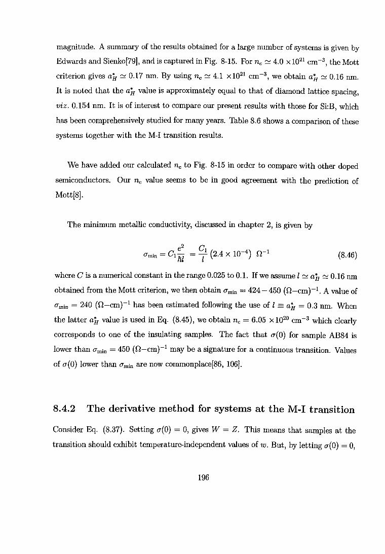
magnitude. A summary of the results obtained for a large number of systems is given by
Edwards and Sienko[79], and is captured in Fig. 8-15. For nc ~ 4.0 x 1021 cm-3 , the Mott
criterion gives a'H ~ 0.17 nm. By using nc ~ 4.1 x1021 cm-3 , we obtain a'H ~ 0.16 nm.
It is noted that the a'H value is approximately equal to that of diamond lattice spacing,
viz. 0.154 nm. It is of interest to compare our present results with those for Si:B, which
has been comprehensively studied for many years. Table 8.6 shows a comparison of these
systems together with the M-1 transition results.
We have added our calculated nc to Fig. 8-15 in order to compare with other doped
semiconductors. Our nc value seems to be in good agreement with the prediction of
Mott[8].
The minimum metallic conductivity, discussed in chapter 2, is given by
e2
cl ( -4) -1 O"min = C1fil = -l 2.4 X 10 f2 (8.46)
where Cis a numerical constant in the range 0.025 to 0.1. If we assume l ~ a'H ~ 0.16 nm
obtained from the Mott criterion, we then obtain O"min = 424-450 (0-cm)-1 . A value of
amin = 240 (!1-cm)-1 has been estimated following the use of l = a'H = 0.3 nm. When
the latter a'H value is used in Eq. (8.45), we obtain nc = 6.05 x 1020 cm-3 which clearly
corresponds to one of the insulating samples. The fact that a(O) for sample AB84 is
lower than O"min = 450 (0-cm)-1 may be a signature for a continuous transition. Values
of a(O) lower than O"min are now commonplace[86, 106].
8.4.2 The derivative method for systems at the M-1 transition
Consider Eq. (8.37). Setting a(O) = 0, gives W = Z. This means that samples at the
transition should exhibit temperature-independent values of w. But, by letting a(O) = 0,
196

102
<! -t::C 0
(/)
:::J
0 <! a:: uJ 10 > .,__ u w LJ... LJ... w
1
14
rn sb
16
s i :p-GaP: z n
n113 4 a* =0.26 c
Ge:As
Sl :As
GaAs:Mn /
w se 2 :Ta
18 20 22
Figure 8-15: Edwards-Sienko plot [79] demonstrating the Mott criterion. The OC:B sample that we have studied is shown against other doped semiconductors in this figure.
197
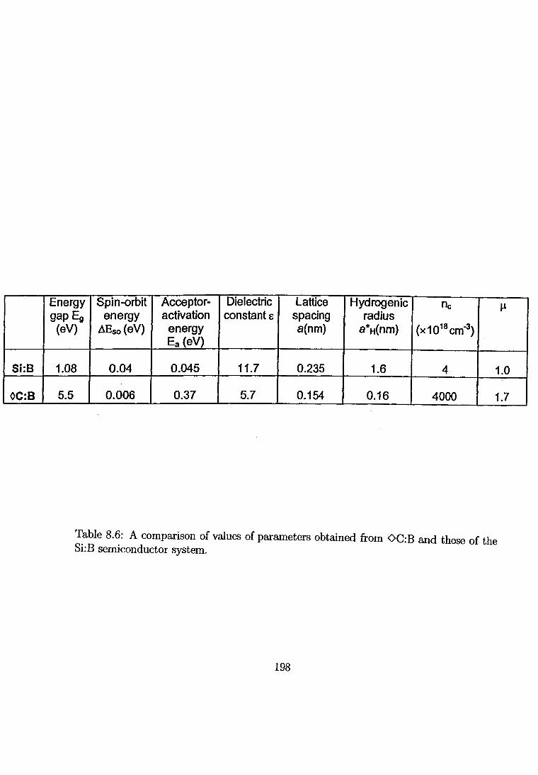
Si:B
OC:B
Energy Spin-orbit Acceptor- Dielectric lattice Hydrogenic nc Jl gap E9 energy activation constant e spacing radius
(eV) AEso(eV) energy a(nm) a*H(nm) (x1018 cm-3)
Ea (eV)
1.08 0.04 0.045 11.7 0.235 1.6 4 1.0
5.5 0.006 0.37 5.7 0.154 0.16 4000 1.7
Table 8.6: A comparison of values of parameters obtained from OC:B and those of the Si:B semiconductor system.
198

the conductivity data can be described by an expression
(8.47)
with C and Z = w being the two fitting parameters. Eq. (8.47) is used to describe
the weakly insulating materials, since CI(T) ~ 0 as T ~ 0 K(206]. The general VRH
law cannot be fitted successfully to weakly insulating samples. According to the scaling
theory of electron localization, setting of CI(O) = 0 should correspond to a continuous M-I
transition. This behaviour has only been observed, to my knowledge, by Zabrodskii(207]
on p-and n-type germanium doped systems, and is still to be reported in other doped
semiconductor systems. By allowing CI(O) to be non-zero, one may obtain some plausible
results, as was recently demonstrated by Rosenbaum et al.[27] and Mobius et al.[13, 14].
We wish to point out that there is still some controversy surrounding this procedure and
one needs to be cautious in analyzing results using this method. The widely used method
involves the extrapolation of CI(T) toT= 0 K(99].
Finite W(T ~ 0) values reflect a vanishing CI(T ~ 0) in accordance with the expo
nential and power laws shown in Eq. (8.48) below. Metallic conduction is indicated by
W(T ~ 0) = 0. Mobius et al.[13, 14] proposed an equation of the general empirical form,
in the case of a discontinuous transition at T = 0 K,
(8.48)
where CI(O, x ~ Xc) = 1 and TEs = 0. By considering the effects of electron-electron
interactions, the exponents m and Z are set to 1/2. The W(T) curves corresponding to
this function were shown in Fig. 7-8. For the highest annealing temperature (1700 ac),
with the data fitted with a solid line, W(T) may tend to zero, which may be taken as
indicative of a continuous transition at T = 0 K. We found that by annealing samples at
high temperatures can drive them towards the M-I transition. Details of Mobius et al.'s
199

method have been given elsewhere[14].
8.5 Compensation of boron-ion impurity centres
It should be noted that some of the boron-ion atoms implanted into diamond get com
pensated by deep-lying donor centres. The values for the boron-ion concentrations that
we have consistently used above could be less than reported. We need to carry out Hall
effect measurements to determine the carrier concentrations in this system. Our efforts
on Hall measurements proved fruitless. The Hall-effect measurements were tried at the
University of Pretoria and Simon Frazer University in Canada at 4 K and 77 K. In both
cases, the concentration of the activated boron-ion centres was lower than expected. The
values of n quote above have been estimated from the SIMS measurements. Instead of
dividing the implanted boron-ion dose with the estimated depth, to determine the concen
trations, we used the following method. To work out n of say sample AB84, we followed
this relation: n(AB84)= D(AB84) xn(AB73)/ D(AB73). Recall that SIMS profiles were
carried out on samples AB73 and AB12. In the case of insulating samples, we used this
relation with results of sample AB12. For those samples which lie in between AB12 and
AB73, an average of these two-values were used to calculate their concentrations.
200

Chapter 9
Conclusions
A summary of the principal results, presented in chapters 5 to 8 on type Ila diamond
specimens which were implanted with boron ions and carbon ions using the CIRA (cold
implantation-rapid-annealing) process, is given in this chapter. I have used the following
notations OC:B to refer to boron-ion implanted diamond specimens and OC:C to re
fer to carbon-implanted diamond specimens. These notations will be used hence-forth.
Suggestions regarding future research work on these systems are made.
Analysis of the OC:B results.
9.1 Insulating samples
On the insulating side of the metal-insulator transition, our experimental results can
be described using phonon-assisted VRH relations. The experimental data follow the
Mott VRH behaviour at high-temperatures (,...., 100 - 300 K) with the hopping exponent
close to m = 1/4. In the temperature range ,...., 1.5- 100 K, the ES VRH conduction
mechanism, with m ~ 1/2, dominates electronic transport processes in the OC:B system.
201

The exponent m = 1/2 is usually associated with the appearance of a Coulomb gap in
the density of states near the Fermi energy. Our experimental results demonstrate the
existence of the conductivity crossover from Mott VRH to ES VRH behaviour as the
temperature is lowered. We have noticed a decrease in the crossover temperature when
the boron-ion concentration is progressively increased. This phenomenon, which has been
investigated over a wide range of doped semiconductors but only observed in a few cases,
may be related to a decrease of the size of the Coulomb gap[168].
The experimental data, on the insulating side of the transition and in the vicinity
of the metal-insulator transition, may be fitted to various scaling functions which were
proposed recently by Aharony et al.[200] and Mobius et al.[13].
9.2 Conduction near the metal-insulator transition
Using the scaling theory of localization described by Eq. (1.1), viz,
u(O)cx (1- :c)~ (9.1)
we determined the critical conductivity exponent to be f.-t "' 1.7. The critical boron-ion
concentration for the metal-insulator transition, nc, was calculated using the Shlimak et
al.[16] method to be nc ~ 4.0 x 1021 cm-3. According to the method ofShlimak et al.[16],
nc can be determined without extrapolating u(T) toT = 0 K although as pointed out
by Sarachik and Bogdanovich[17] extrapolation of u(T) to T = 0 K is preferable.
202

9.3 Conduction in the metallic regime
The temperature dependence of our low-temperature conductivity data follows the
conventional expression given by Eq. (2.11), which is
a(T) = a(O) + CTz (Z = 1/2 or 1/3) (9.2)
Higher order terms associated with weak inelastic scattering have been dropped in Eq.
(9.2) due to their insignificant contribution in our system. We found the conductivity
exponent of Z = 1/3 gives a better fit to our low temperature experimental data than
Z = 1/2 sample at nc. In the case of samples n > nc, Z = 1/3 gives a better fit to the
data than Z = 1/2.
9.4 High-temperature annealing
The resistance (or conductivity) showed a remarkable improvement when samples
were annealed at temperatures above 1200 °C. The drop in resistivity has been associ
ated with two phenomena: (i) the diminishing of the compensating centres with high
temperature annealing cycles and/or (ii) the reduction in the lattice disorder in OC:B
system. The origin and the nature of the vacancy-related compensating centres are still
not well understood.
203

Analysis of the <>C:C results.
9. 5 Percolation transition
Our experimental results seem not to follow a sharp percolation model suggested by
Kalish et al.[143], indicating that the transformation of diamond from a highly insulating
state into a highly conducting phase may be less precipitate than suggested by a simple
percolation model[219].
On the insulating side the transition, our experimental data show VRH type behav
iour, with an apparent conductivity crossover as the temperature is lowered.
9.6 Future Directions
A variety of options in the implantation-annealing routine need to be tested in <>C:B
and <>C:C systems. Only the CIRA Technique was pursued in this study. Various au
thors have characterized their diamond specimens using various implantation-annealing
procedures[116, 145]. Annealing of samples beyond 1700 °C proved unsuccessful, owing
to a milky-colour that developed on the implanted surface. Alternative ways of annealing
at high temperature need to be explored.
Electrical conductivity measurements need to be extended to the millikelvin range in
order to extract reliable exponent and other information from the u(T) plots. Effects
due to weak-localization may also be examined in this system.
The actual boron-ion concentrations, participating in the conduction processes, were
204

not known precisely in our system. The net concentration of the boron concentration was
measured using SIMS analysis. The latter technique has disadvantages. Besides being
destructive to the very surface it intends to probe, the SIMS spectroscopy cannot resolve
the precise location of the trace element as to whether it resides in a substitutional or
interstitial lattice site. This means that Hall-effect measurements are needed on these
samples to determine the density of the activated boron atoms.
Magnetoresistance measurements should also be made in this system. We made
measurements in OC:B samples in the presence of a 1 T field, and the results proved
inconclusive.
9. 7 Published papers
The work carried out in this research project culminated into a number of presentations
in local and international conferences. The following articles have been published:
M. J. R. Hoch, T. Tshepe, and J. F. Prins, Ann. Phys. (Leipzig) 8, (1999) in print.
T. Tshepe, J. F. Prins and M. J. R. Hoch, Diamond and Related Materials 8, 1508
(1999).
T. Tshepe, J. F. Prins and M. J. R. Hoch, Czech. J. Phys. 46, 2439 (1996), Suppl.
S5.
T. Tshepe, J. F. Prins and M. J. R. Hoch, Czech. J. Phys. 46, 2441 (1996), Suppl.
S5.
In preparation:
T. Tshepe and M. J. R. Hoch, to be submitted to Phys. Rev. B.
J. Wu, T. Tshepe and M. J. R. Hoch, J. E. Butler, to be submitted to Phys. Rev.
B.
205

Bibliography
[1] D. R. MacKenzie, D. A. Muller, E. Kravtchinskaia, D. Segal, D. J. H. Crockayne,
G. Amaratunga and R. Silva, Thin Solid Films 206, 198 (1991).
[2] S. Tolansky, The History and Use of Diamond (The Shenval Press, London, 1962);
R. C. Eden, Diamond and Relat. Mater. 2, 1051 (1993).
[3] J. E. Field, The Properties of Natural and Synthetic Diamond, edited by J. E. Field
(Academic Press, London,1992).
[4] J. F. Prins, in Int. School of Phys. "Enrico Fermi" Course CXXXV-The Physics of
Diamond, edited by A. Paoletti and A. Tucciarone (lOS Press, Amsterdam, 1997)
p. 411.
[5] M. S. Dresselhaus and R. Kalish, Ion Implantation in Diamond, Graphite and
Related Materials (Springer Series in Materials Science 22, Springer-Verlag,
Berlin, 1992).
[6] J. F. Prins, Phys. Rev. B 38, 5576 (1988).
[7] J. F. Prins, Nuclear Instrum. and Methods B 35, 484 (1988); Nuclear Instrum. and
Methods in Phys. Research B, in press.
[8] N. F. Mott, Metal-Insulator Transitions (Taylor and Francis, London, 1990).
[9] P. W. Anderson, Phys. Rev. 109, 1492 (1958).
206

[10] A. F. Ioffe and A. R. Regel, Proc. Sernicond. 4, 237 (1960).
[11] E. Abrahams, P. W. Anderson, D. C. Licciardello and T. V. Ramakrishnan, Phys.
Rev. Lett. 42, 693 (1979).
[12] A. Mobius, D. Elefant, A. Heinrich, R. Muller, J. Schumann, H. Vinzelberg and G.
Zies, J. Phys. C: Solid State Phys. 16, 6497 (1983).
[13] A. Mobius, C. Frenzel, R. Thielsch, R. Rosenbaum, C. J. Adkins, M. Schreiber,
H.-D, Bauer, R. Grotzschel, V. Hoffmann, T. Krieg, N. Matz, H. Vinzelberg and
M. Witcomb, Proc. 24th Int. Conf. Phys. of Semicond. Jerusalem, Israel, 1998.
[14] A. Mobius and C. J. Adkins, Current Opinion in Sold State and Mater. Sci. 4, 303
(1999).
[15] G. A. Thomas, Phil. Magazine B 52, 479 (1985).
[16] I. Shlimak, M. Kaveh, R. Ussyshkin, V. Ginodman and L. Resnick, Phys. Rev.
Lett. 77, 1103 (1996).
[17] M P. Sarachik and S. Bogdanovich, Phys. Rev. Lett. 78, 3977 (1997).
[18] T. F. Rosenbaum, K. Andries, G. A. Thomas and R. N. Bhatt, Phys. Rev. Lett.
45, 1723 (1980).
[19] M. J. Hirsch, U. Thomanschefsky and D. F. Holcomb, Phys. Rev. B 37, 8257
(1988).
[20] A. T. Collins, in ref. [4]; M. A. Omar, Elementary Solid State Physics (Addison
Wesley Publishing Company, 1975).
(21] A. T. Collins, in Properties and Growth of Diamond, edited by Gordon Davies
(Published by INSPEC, the Institution of Electrical Engineers, London, United
Kingdon, 1994), chapt. 9, p. 261.
207

(22] M. Werner and R. Locher, Rep. Prog. Phys. 61, 1665 (1998).
(23] B. I. Shklovskii and A. L. Efros, Electronic Properties of Doped Semiconductors
(Springer Series in Solid State Science 45, Springer-Verlag, Berlin, 1984).
[24] H. Bottger and V. V. Bryksin, Hopping Conduction in Solids (VCH Publishers,
Academie-Verlag, Berlin, 1985).
[25] D. Belitz and T. R. Kirkpatrick, Rev. Modern Phys. 66, 261 (1994).
[26] Uwe Hans Thomanschefsky, PhD Thesis (Cornell University, Ithaca, New York,
1990), Chapt. 2, p. 10.
[27] R. Rosenbaum, N. V. Lien, M. R. Graham and M. Witcomb, J. Phys. Condens.
Matter 9, 6247 (1997).
(28] R. Rosenbaum, A. Heines, M. Karpovskii, M. Pilosof and M. Witcomb, J. Phys.
Condens. Matter 9, 5413 (1997).
[29] R. Rosenbaum, A. Heines, A. Palevskii, M. Karpovskii, A. Gladkikh, M. Pilosof, A.
J. Daneshvar, M. R. Graham, T. Wright, J. T. Nicholls, C. J. Adkins, M. Witcomb,
V. Prozesky, W. Przybylowicz and R. Pretorius, J. Phys. Condens. Matter 9, 5395
(1997).
[30] R. L. Rosenbaum, N. V. Lien, M. R. Graham and M. Witcomb, Phys. sol. (b) 205,
41 (1998).
[31] A. Mobius, H. Vinzelberg, D. Elefant, J. Schumann and G. Zies, J. Phys. C 18,
3337 (1985).
[32] A. Mobius, J. Phys. C 18, 4639 (1985).
[33] A. Mobius, J. Phys. C 19, L147 (1986).
[34] A. Mobius, Non Cryst. Solids 97+98, 483 (1987).
208

(35] A. Mobius, Phys. Rev. B 40, 4194 (1989).
(36] A. M. Finkel'shtein, Sov. Phys. JETP 57, 97 (1983).
[37] A. L. Efros and B. I. Shklovskii, J. Phys. C 8, L49 (1975).
(38] M. Pollak, Discuss. Faraday Soc. 50, 13 (1970).
(39] G. Srinivasan, Phys. Rev. B 4, 2581 (1971); R. Chocon, M. Ortuno and M. Pollak,
Phys. Rev. B 37, 10520 (1988).
(40] T. Kurosawa and K. Sugimoto, Prog. Theor. Phys. Suppl. 57, 217 (1975).
(41] A. Perez-Garrido, M. Ortuno, E. Cuevas, J. Ruiz and M. Pollak, Phys. Rev. B 55,
8630 ( 1997).
(42] A. L. Efros and B. I. Shklovskii, J. Phys. C 8, 249 (1975).
(43] M. Pollak, Phil. Magazine B 65, 657 (1992).
[44] M. Pollak and M. Ortuno in Electron-Electron Interactions in Disordered Systems,
edited by M. Pollak and A. L. Efros (North-Holland, Amsterdam, 1985) chapt. 4,
p. 287. The reader is referred also to a chapter by A.L. Efros and B. I. Shklovskii
in this book.
[45] Masatoshi Imada, Atsuhi Fujimori and Yoshunori Tokura, Rev. Modern Phys. 70,
1039 (1998).
(46] J. G. Massey and Mark Lee, Phys. Rev. Lett. 75, 4266 (1995).
(47] Conf. Proc. Hopping and Related Phenomena, published in Phys. sol. (b) 205,
(1998).
(48] Phil. Trans. R. Soc. London A 356, (1998).
[49] N. F. Mott, J. Non-Cryst. Solids 1, 1 (1968).
209

[50] Vinay Ambegaokar, B. I. Halperin and J. S. Langer, Phys. Rev. B 4, 2612 (1971).
[51] N. F. Mott and E. A. Davis, Electronic Processes in Non-Crystalline Materials
(Claredon, Oxford, 1979).
[52] E. M. Hamilton, Phil. Magazine 26, 1043 (1972).
[53] Ju-Jin Kim and Hu Jong Lee, Phys. Rev. Lett. 70, 2798 (1993).
[54] E. Cuevas, M. Ortuno and M. Pollak, Phys. Rev. B 45, 11542 (1992).
[55] J. Ruiz, M. Ortuno and E. Cuevas, Phys. Rev. B 48, 10777 (1993).
[56] M. Pollak and M. L. Knotek, Solid State Commun. 21, 183 (1977).
[57] V. L. Nguyen and B. I. Shklovskii, Sov. Phys. Semicond.13, 1281 (1979).
[58] M. L. Knotek and M. Pollak, Phys. Rev. B 9, 664 (1974).
[59] K. Tenelsen and M. Schreiber, Phys. Rev. B 49, 12662 (1994).
[60] R. Chicon, M. Ortuno and M. Pollak, Phys. Rev. B 37, 10520 (1988).
[61] S.D. Baranovskii, B. I. Shklovskii and A. L. Efros, Sov. Phys. JETP 51, 199 (1980).
[62] J. H. Davies, Phil. Magazine B 52, 511 (1985).
[63] K. Tenelsen and M. Schreiber, Phil. Magazine 65, 695 (1992).
[64] K. Tenelsen and M. Schreiber, Phys. Rev. B 52, 13287 (1995).
[65] A. N. Ionov, M. J. Lea and R. Rentzsch, JETP Lett. 54, 473 (1991).
[66] I. Terry, T. Penny, S. von Molnar and P. Besla, Phys. Rev Lett. 69, 1800 (1992).
[67] B. L. Al'tshuler and A. G. Aronov, Solid State Commun. 30, 115 (1979); Sov. Phys.
JETP 50, 960 (1979); Sov. Phys. JETP Lett. 30, 482 (1979).
210

[68] G. A. Thomas, A. Kawabata, Y. Ootuka, S. Katsumoto, S. Kobayashi and W.
Sasaki, Phys. Rev. B 26, 2113 (1982).
[69] B. L. Al'tshuler and A. G. Aronov, JETP Lett. 37, 410 (1983).
[70] P. A. Lee and T. V. Ramakrishnan, Rev. Modern Phys. 57, 287 (1985).
[71] C. Castellani, C. DiCastro, H. Fukuyama, P. A. Lee and M. Ma, Phys. Rev. B 33,
7277 (1986).
[72] Albert Schmid, Z. Physik, 271, 251 (1974).
[73] D. Belitz and K. I. Wysokinski, Phys. Rev. B 36, 9333 (1987).
[74] R. M. Hill, Phys. Stat. Sol. A 35, K29, (1976); ibid. 34, 601 (1976).
[75] R. Hill and Jonscher, J. Non-Cryst. Solids 32, 53 {1979).
[76] A. G. Zabrodskii and K. N. Zinov'eva, Soviet Phys. JETP 59, 425 {1984).
[77] J. Hubbard, Proceeding of Royal Soc. A (London) 276, 238 (1963).
[78] N. F. Mott, Conduction in Non Crystalline Materials {Oxford, London, 1993).
[79] P. P. Edwards and M. J. Sienko, Phys. Rev. B 17, 2575 (1978).
[80] J. Hubbard, Proceeding of Royal Soc. A {London) 277, 237 (1964); ibid. 281, 401
{1964).
[81] D. J. Thouless, Phys. Reports C 13, 93 (1974).
[82] F. J. Wegner, Z. Physik B 25, 327 {1976).
[83] G. J. Dolan and D. D. Osheroff, Phys. Rev. Lett. 43, 721 (1979).
[84] N. Giordano, Phys. Rev. Lett. B 22, 5635 (1980).
211
[85] T. F. Rosenbaum, G. A. Thomas and M. A. Paalanen, Phys. Rev. Lett. 72, 2121
(1994).
[86] H. Stupp, M. Hornung, M. Lakner, 0. Madel and H. v. Lohneysen, Phys. Rev.
Lett. 71, 2634 (1993).
(87] P. Dai, Y. Zhang and M. P. Sarachik, Phys. Rev. Lett. 67, 136 (1991).
[88] P. Dai, Y. Zhang and M.P. Sarachik, Phys. Rev. Lett. 66, 1914 (1991); Phys. Rev.
B 45, 3984 (1992).
[89] P. Dai, Y. Zhang and M. P. Sarachik, Phys. Rev. B 49, 14039 (1994); Phys. Rev.
Lett. 70, 1968 (1993)
[90] A. P. Long and M. Pepper, J. Phys. C 17, L425 (1984).
[91] D. Belitz and T. R. Kirkpatrick, Phys. Rev. B 52, 1392 (1995).
[92] T. G. Castner, Phys. Rev. Lett. 88, 1539 (2000); ibid. 84 2905 (2000).
(93] C. Castallani, G. Kotliar and P. A. Lee, Phys. Rev. Lett. 59, 323 (1987).
[94] C. Castallani, C. DiCastro, P. A. Lee and M. Ma, Phys. Rev. B 30, 527 (1984).
[95] S. Hikami, Phys. Rev. B 24, 2671 (1981).
[96] W. Sasaki, in Z Localization, edited by T. Ando and H. Fukuyama (Springer-Verlag,
Berlin, 1988) p. 11.
[97] W. L. McMillan and J. Mochel, Phys. Rev. Lett. 46, 556 (1981).
[98] G. Hertel, D. J. Bishop, E. G. Spencer, J. M. Rowell and R. C. Dynes, Phys. Rev.
Lett. 50, 743 (1983).
[99] G. A. Thomas, Y. Ootuka, S. Katsumoto, S. Kobayashi and W. Sasaki, Phys. Rev.
B 25, 4288 (1982).
212

[100] U. Thomanschefsky and D. F. Holcomb, Phys. Rev. B 45, 13356 (1992).
[101] P. Dai, Y. Zhang, S. Bogdanovich and M. P. Sarachik, Phys. Rev. B 48, 4941
(1993).
[102] P. F. Newman and D. F. Holcomb, Phys. Rev. Lett. 51, 2144 (1983).
[103] D. W. Koon and T. G. Castner, Phys. Rev. Lett. 60, 1755 (1988).
[104] T. G. Castner, in Hopping Transport in Solids, edited by M. Pollak and B. I.
Shklovskii (Elsevier/ North-Holland, Amsterdam, 1991), p. 1; Phys. Rev. B 52,
12434 (1995).
[105] K. M. Itoh, E. E. Haller, J. W. Beeman, W. L. Hansen, J. Emes, L.A. Reichertz,
E. Kreysa, T. Shutt, A. Cummings, W. Stockwell, B. Sadoulet, J. Muto, J. W.
Farmer, V. I. Ozhogin, Phys. Rev. Lett. 77, 4058 (1996).
[106] R. Rosenbaum, M. Slutzky, A. Mobius and D. S. McLachlan, J. Phys. Condens.
Matter 6, 7797 (1994).
[107] Private communication with Prof. M. J. R. Hoch following his discussions with
Prof. T. G. Castner and Prof. D. Holcomb (1999).
[108] M. C. Maliepaard, M. Pepper, R. Newbury and G. Hill, Phys. Rev. Lett. 61, 369
(1988).
[109] N. F. Mott, Phil. Magazine 26, 1015 (1972).
[110] G. A. Thomas, M. Paalanen and T. F. Rosenbaum, Phys. Rev. B 27, 3897 (1983);
T. F. Rosenbaum, K. Andries, G. A. Thomas and R. N. Bhatt, Phys. Rev. Lett.
45, 1723 (1980); M. Paalanen, T. F. Rosenbaum, G. A. Thomas and R.N. Bhatt,
Phys. Rev. Lett. 48, 284 (1982).
[111] J. S. Langer and T. Neal, Phys. Rev. Lett. 16, 984 (1966).
213

[112] T. Neal, Phys. Rev. 169, 508 (1968).
[113] Gerd Bergmann, Phys. Reports 107, 1 (1984).
[114] A. Kawabata, Solid State Commun. 34, 431 (1980); J. Phys. Soc. Japan 49, 628
(1980).
[115] B. I. Al'tshuler and A. G. Aronov, in Electron-Electron Interactions in Disordered
Systems, edited by M. Pollak and A. L. Efros (North-Holland, Amterdam, 1985)
chapt. 1, p. 1.
[116] V. S. Vavilov, M. I. Guseva, E. A. Konorova, V. V. Krasnopevtsev, V. F. Sergienko
and V. V. Thtov, Sov. Phys. Solid State 8, 1560 (1966).
[117] J. F. Prins, Diam. and Relat. Mater. 5, 907 (1996).
[118] J. F. Prins Mater. Sc. Rep. 7, 271 (1992).
[119] J. F. Prins, Phys. Rev. B 31, 2472 (1985).
[120] J. F. Prins, Phys. Rev. B 44, 2470 (1991).
(121] J. Koike, D. M. Parkin and T. E. Mitchell, Appl. Phys. Lett. 60, 1450 (1992).
(122] J. F. Prins, Thin Solid Films 212, 11 (1992).
[123] J. F. Prins, Physica B 185, 132 (1993).
[124] J. F. Prins, Nuclear Instrum. and Methods Phys. Res. B 80/81, 1433 (1993).
[125] J. F. Prins, Nuclear Instrum. and Methods B 35, 484 (1993); J. F. Prins, Nuclear.
Instrum. and Methods Phys. Res. B 80/81, 1433 (1993).
[126] J. F. Prins, Nuclear. Instrum. and Methods B 59/60, 1387 (1991).
[127] J. F. Prins, Diam. and Relat. Mater. 9, 1835 (2000).
214

[128] J. J. Hauser and J. R. Patel, Solid State Commun. 18, 789 (1976).
[129] S. Prawer and R. Kalish, Phys. Rev. B 51, 15711 (1995).
[130] R. S. Nelson, J. A. Hudson and D. J. Mazey, British Patent no. 1599668 (1981).
[131] R. A. Spitz, T. E. Derry, J. F. Prins and J. P. F. Sellschop, Nuclear Instrum. and
Methods B 51, 1366 (1990).
[132] R. Zeidler, C. A. Hewett and R. G. Wilson, Phys. Rev. B 47, 2065 (1993).
[133] J. F. Prins, Phys. Rev. B 39, 3764 (1989).
[134] H. B. Dyer and F. Ferdinanda Br. J. Appl. Phys. 17, 419 (1996).
[135] E. W. Maby, C. W. Magee and J. H. Morewood, Appl. Phys. Lett. 39, 157 (1981).
[136] J. F. Prins, T. E. Derry and J. P. F. Sellschop, Phys. Rev. B 34, 8870 (1986).
[137] J. F. Prins, T. E. Derry and J. P. F. Sellschop, Nuclear. Instrum. and Methods
Phys. Res. B 18, 261 (1987).
[138] J. F. Ziegler, J. P. Biersack and U. Littmark, The Stopping and Range of Ions in
Solids (Pergamon Press, New York, 1985).
[139] J. F. Prins, Nucl. Instrum. Methods B 59/60, 1387 (1991).
(140] Robert C. Richardson and Eric. N. Smith, Experimental Techniques in Condensed
Matter Physics at Low Temperatures (Addison-Wesley Publishing Company, New
York, 1988).
[141] D. S. Betts, Refrigeration and Thermometry Below One Kelvin (Sussex University
Press, 1976).
(142] Anthony Kent, Experimental Low Temperature Physics (MacMillan Physical Sci
ences Series, The MacMillan Press, Ltd., Kent, Great Britain, 1993).
215

[143] R. Kalish, T. Bernstein, B. Shapiro and A. Talmi, Radiation Effects 52, 153, (1980).
[144] J. J. Hauser, J. R. Patel and J. N. Rogers, Appl. Phys. Lett. 30, 129 (1977).
[145] R. Kalish, in Int. School of Phys. "Enrico Fermi" Course CXXXV-The Physics of
Diamond, edited by A. Paoletti and A. Thcciarone (lOS Press Amsterdam, 1997).
[146] R. Kalish, Diam. and Relat. Mater. 2, 621 {1993).
[147] R. Kalish, in Properties and Growth of Diamond (Published by INSPEC, the In
stitution of Electrical Engineers, London, United Kingdom, 1994) chapt. 6, p. 189.
(148] A. Hoffman, S. Prawer and R. Kalish, Phys. Rev. B 45, 12736 (1992).
[149] J. F. Prins, Diam. and Relat. Mater. 3, 922 (1994).
[150] J. F. Prins, Appl. Phys. Lett. 76, (2000) in press.
[151] S. R. Broadbent and J. M. Hammersley, Proc. Cambridge, Phil. Soc. 53,629 (1957).
[152] V. K. S. Shante and S. Kirkpatrick, Adv. Phys. 20, 325 (1971).
[153] S. Kirkpatrick, Rev. Modern Phys. 45, 574 (1973).
[154] J. W. Essam, Rep. Prog. Phys. 43, 833 {1980).
[155] D. J. Bergman and D. Stroud, in Solid State Physics, edited by H. Ehrenneich and
D. Thrnbull (Academic Press, San Diego, 1992).
[156] D. S. Stauffer and A. Aharony, Introduction to Percolation Theory, 2nd Edition,
(Taylor and Francis, 1994). The reader is referred also to a paper by P. Smilauer,
Contemporary Physics 32, 89 (1992).
(157] R. P. Kusy, J. Appl. Phys. 48, 5301 {1977).
[158] C. Domb, E. Stoll and T. Schneider, Comtemporary Physics 21, 577 {1980).
216

---
[159] J. M. Hammersley and D. J. A. Welsh, Contemporary Physics 21, 593 (1980).
[160] I. Balberg, Phil. Magazine B 56, 991 (1987).
[161] z. Ball, H. M. Phillips, D. L. Callahan and R. Sauerbrey, Phys. Rev. Lett. 73, 2099
(1994).
[162] A. Y. Dovzhenko and P. V. Zhirkov, Phys. Lett. A 204, 247 (1995).
[163) D. S. Stauffer, Introduction to Percolation Theory, (Taylor and Francis, 1985).
[164) A. Carl, G. Dumpich and E. F. Wassermann, Thin Solid Films 17 4, 225 (1989).
[165) Ce-Wen Nan, Prog. Mater. Science 37, 1 (1993).
[166) M. B. Heaney, Phys. Rev. B 52, 12477 (1995); G. Deutscher, A. Kapituinik and
M. Rappaport, in Percolation Structures and Processes, edited by G. Deutscher,
R. Zallen and J. Adler (Annals of the Israel Phys. Soc. 5, 1983), chapt. 10, p. 207.
[167] S. Prawer, A. Hoffman, M. Petravic and R. Kalish, J. Appl. Phys. 73, 3841 (1993).
[168] Y. Zhang, P. Dai, M. Levy and M. P. Sarachik, Phys. Rev. Lett. 64, 2687 {1990).
[169) M. Paalanen, T. F. Rosenbaum, G. A. Thomas and R.N. Bhatt, Phys. Rev. Lett.
48, 284 (1982).
[170] C. J. Adkins, J. Phys. Condens. Matter 1, 1253 {1989).
[171] C. J. Adkins, J. Phys. Condens. Matter 1, 123 (1990).
[172] C. J. Adkins, in Hopping and Related Phenomena, edited by H. Fritzche and M.
Pollak (World Scientific Publishing, 1990) p. 93.
[173) J. C. Dawson and C. J. Adkins, J. Phys. Condens. Matter 7, 6297 (1995); T.
Frauenheim, U. Stephanu, K. Beuriloga, F. Jungnickel, P. Blaudeck and E. Fromm,
Thin Solid Films 182, 63 (1989).
217

[174] R. Rosenbaum, Phys. Rev. B 44, 3599 (1991).
[175] Y. Meir, Phys. Rev. Lett. 77, 5265 (1996).
[176] C. H. Olk, S. M. Yalisove, J. P. Heremans and G. L. Doll, Phys. Rev. B 52, 4643
(1995).
[177] Private Communication with Prof Boris A. Aronzon {1998).
[178] M. Watanabe, Y. Ootuka, K. M. Itoh and E. E. Haller, Phys. Rev. B 58, 9851
(1998).
[179] E. A. Davis and W. D. Compton, Phys. Rev. 140, A2183 (1965).
[180] W. Sasaki andY. Yamanouchi, J. Non Cryst. Solids 4, 183 (1970).
[181] F. R. Allen and C. J. Adkins, Phil. Magazine 26, 1027 (1972).
[182] P. T. Wedepohl, Proc. Phys. Soc. B 70, 177 (1957); C. J. Rauch, Phys. Rev. Lett.
7, 83 (1961).
[183] J. F. Prins, Phys. Rev. B 61, 1 (2000).
[184] M. I. Buraschi, G. U. Pignatel and S. Sanguinetti, J. Phys.: Condens. Matter 2,
10011 (1990).
[185] Private communications with Dr. Anoulf Mobius and Prof Ralph Rosenbaum at
the 24th International Conference on the Physics of Semiconductors (ICPS24) held
in Jerusalem, Israel (1998). See also re£.[221].
[186] J. Shoshany, V. Goldner, R. Rosenbaum, M. Witcomb and D. S. McLachlan, J.
Phys. Condens. Matter 8, 1729 (1996).
[187] H. White and D. S. McLachlan, J. Phys. C: Solid State Phys. 19, 5415 (1986).
[188] R. A. Davies, M. Pepper and M. Kaveh, J. Phys. C: Solid State Phys. 16, L285.
218

[189] H. Akima, J. of A.C. M. 17, 589 (1970).
[190] B. Kramer and A. Mackinnon, Rep. Progress in Physics 56, 1469 (1993).
[191] S. J. Lee, J. B. Ketterson and N. Trivedi, Phys. Rev. B 46, 12695 (1992).
[192] N. V. Lien and R. Rosenbaum, Phys. Rev. B 56, 14960 (1997); N. V. Lien, Phys.
Lett. 207, 379 (1995).
[193] J. G. Massey and M. Lee, Phys. Rev. Lett. 75, 4266 (1996).
[194] M. Hornung and H. v. Lohneysen, Czech. J. Phys. 46, 2437 (1996), Suppl. S5.
(195] N. F. Mott, in [8], p50.
[196] N. F. Mott, in [78], p32.
[197] A. S. Skal and B. I. Shklovskii, Sov. Phys.: Solid State 16, 1190 (1974).
[198] M. Ortuno and M. Pollak, J. Non Crystalline Solids 59+60, 53 (1983).
[199] A. L. Efros and B. I. Shklovskii, J. Phys. C 8, L49 (1975).
[200] A. Aharony, Y. Zhang and M. P. Sarachik, Phys. Rev. Lett. 68, 3900 (1992).
[201] S. Bogdanovich, M. P. Sarachik, R. N. Bhatt, Phys. Rev. Lett. 82, 137 (1999).
[202] S. Bogdanovich, D. Simonian, S. V. Kravchenko, M. P. Sarachik, R. N. Bhatt,
Phys. Rev. B 60, 2286 (1999).
[203] S. Bogdanovich, M. P. Sarachik, R. N. Bhatt, Phys. Rev. B 60, 2292 (1999).
[204] P. A. Lee and T. V. Ramakrishnan, Rev. Modern Phys. 57, 287 (1985).
[205] T. G. Castner and W. N. Shafarman, preprint, to be submitted for publication
(2000).
219

[206] J. R. Friedman, Y. Zhang, P. Dai and M. P. Sarachik, Phys. Rev. B 53, 9528
(1996).
(207] A. G. Zabrosdkii, Sov. Phys. Semicond. 14, 670 (1980); ibid 14, 781 (1980).
(208] M. B. Isichenko, Rev. Modern Phys. 64, 961 (1992).
(209] H. Ryssel and I. Ruge, Ion Implantation (Wiley, New York, 1986).
(210] V. S. Vavilov, M. I. Guseva, E. A. Konorova, V. V. Krasnopevtsev, V. F. Sergienko
and V. V. Tutov, Soviet Phys. Semicond. 4, 6 (1970) ; ibid 12; L.A. Davidson, S.
Chou, J. F. Gibbons and W. S. Johnson, Radiation Effect 7, 35 (1971).
[211] C. Uzan-Saguy, C. Cytermann, R. Brener, V. Ritcher, M. Shaanan and R. Kalish,
Appl. Phys. Lett. 67, 1194 (1995).
[212] A. G. Zabrodskii and K. N. Zinov'eva, Soviet Phys. JETP 59, 425 (1984).
[213] S. Prawer, A. Hoffman and R. Kalish, Appl. Phys. Lett. 57, 2187 (1990).
(214] B. I. Shklovskii and A. L. Efros, in [23] p206 and p240.
(215] G. Davies, Nature 269, 494 (1977).
(216] Private communication with Prof J. F. Prins (1998).
[217] See the remarks made by A. Mobius to Dr. G. Kotliar in Phil. Trans. R. Soc.
London A 356, 73 (1998); see also, P. P. Edwards, R. L. Johnston, C. N. R. Rao,
D. P. Tunstall and F. Hensel, Phil. Trans. R. Soc. London A 356, 3 (1998).
[218] Private communication with Prof Ralph Rosenbaum (1996).
(219] T. Tshepe, J. F. Prins and M. J. R. Hoch, Czech. J. Phys. 46, 2441 (1996), Suppl.
85.
220

[220] A. T. Collins and E. C. Lightowlers, in The Properties of Natural and Synthetic
Diamond, edited by J. E. Field (Academic Press, London,1979) p. 79; J. F. H.
Custers, Physica 18, 489 (1952).
[221] P. P. Edwards, R. L. Johnston, C. N. R. Rao, D. P. Thnstall and F. Hensel, Phil.
Trans. R. Soc. London A 356, 3 (1998); Note the remarks made by Dr. A. Mobius
to Dr. G. Kotliar on page 73 of the same Journal.
[222] J. C. Bourgoin and J. Walker, Industrial Diamond Review 362 (1976).
221


![A Study on Distributions of Boron Ions Implanted by Using B · PDF filesimulation [7-9], and the results were compared with secondary ion mass spectrometry (SIMS) data. UT-Marlowe](https://img.dokumen.tips/doc/110x75/5a9111897f8b9afe568e63ad/a-study-on-distributions-of-boron-ions-implanted-by-using-b-7-9-and-the-results.jpg)