Embed Size (px)
Citation preview
.r
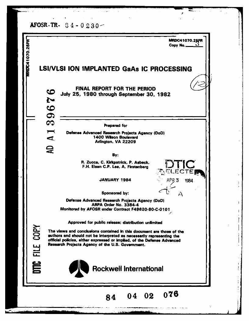
AFOSR-TR. 3 4 -0 2 3 0-
MRDC41 070.2 KfRso Copy No.J-.
LSI/VLSI ION IMPLANTED GaAs IC PROCESSING
FINAL REPORT FOR THE PERIODJuly 25, 1980 through September 30, 1982
COD Prepared for
?Defense Advanced Research Projects Agency (DoD)01, 1400 Wilson Boulevard
Arlington, VA 22209
By:
R. Zucca, C. Kirkpatrick, P. Asbeck,F.H. Eisen C.P. Lee, A. Firstenberg 0ITrLECTE0114
JANUARY 1984 APR 3 1984
Sponsored by: ADefense Advanced Research Projects Agency (DoD)
ARPA Order No. 3384-4Monitored by AFOSR under Contract F49620-80-C-0101
/
Approved for public release; distribution unlimited
0 The views and conclusions contained in this document are those of theC authors and should not be interpreted as necessarily representing the
- official policies, either expressed or implied, of the Defense Advanced
ILL Research Projects Agency of the U.S. Government.ILL.
C.3 ARockwell International
84 04 02 076
UNCLASSIFIEDSECURITY CLASSIFICATION OF THIS PAGE
REPORT DOCUMENTATION PAGEI& REPORT SECURITY CLASSIFICATION 1b. RESTRICTIVE MARKINGS
Unclassified2&. SECURITY CLASSIPICATION AUTHORITY 3. OISTRI@UTION/AVAILAEILITY OF REPORT
_________________________________________ Approved for public release; distribution unlimited.
2. OCLASSIFICATION/DGWNGRAOING SCH4EDULE This research was sponsored by the Defense AdvancedResearch Projects Agency (DoD) ARPA Order No. 3384-4
6. PERFORMING ORGANIZATION REPORT NUMSER(11S) S. MONI1TORING ORGANIZATION REPORT NUMEISI11
MRDC4107O.25FR AFOSR-TR -- ' ^_:nGa. NAM4 OF Pf AFORMING0 ORGANIZATION 66 OFFICE SYMBOL IT& NAME Of MONITORING ORGANIZATION
Rockwel international t*DU6.IAir ForceMicroelectronics Research and IOfc fSinii eerhwDevelopmentCenter Office____of __Scientific_____Research___
oc. ADDRESS (cty. State and ZIP C~i.A 7b. ADDRESS (City. Sata &%ad ZIP C..dh
1049 Camino Dos Rios Boiling Air Force BaseThousand Oaks, California 91360 Washington, DC 20332
I&. NAME OFP UNOING/SPONSORING 81Sb. OFFICE SYMBOL S. PROCUREMENT INSTRUMENT IDENTIFICATION NUMIERORGANIZATION "f 'applicabic)Cnrc o F92-OC00Defense Advanced Research CotatN.F92-0C00Projects Agency MDOM) I
ft. ADORSS Cily. dialir and ZIP Codu) 10 SOURCE OF FUNDING NOS.
1400 Wilson Boulevard PRO0GRAM PROJECT TASK WORK UNITArlington, VA 22209 ELEMENT NO. NO. NO. NO.
11. TITLE *nciIude SecuiPty CZ.mificesioni,
LSI/VLSI ION IMPLANTED GaAs IC PROCESSING (U)12. PERSONAL AUTMORCS)
Zucca, Ricardo R.; Kirkpatrick, Cornileeo; Asbeck, Peter M.; 6sean, Fied +l.- Lea, Chle-Ping; Firstenberg, Allen13& TYPE 0F REPORT 13&. Time COVERED 14. DATE OF REPORT 1Yr. .. a S PAGE COUNT
Final Report FRP om 07/25/80 TO 09/30/82 January 1984 7 73631S. SMPPLEMENTARV NOITATION
Theo views and conclusions contained in this document are those of the authors and should not be interpreted as necessarilyrepresenting the official policies, either expressed or implied, of the Defense Advanced Research Projects Agency of theU.S. government.
17 COSATI CODES 18. SUBJECT TERMS 'ContinAm on roversit if neceaW7 and identnfy by black nsimberl
FIELD GROUP I sue. GR. ISemi-insulating, ion implantation, IC, integrated circuits, high speed logic,
1 0 GaAs, FET, r i:SFET19. A)STRACT iConianuc on ivey..i. owtsegrP and iden ufy by bMaCk nuomb.,,
This report covers a program designed to realize the full potential of GaAs integrated circuits by expandingand improving fabrication and material techniques. The main accomplishment of the program was the success-ful implementation of the fabrication of integrated circuits on 3-inch diameter GaAs wafers. In addition,this program covered many activiti releaed to GaAs IC processing. These include: work on semi-insulatingmaterial growth and characterization. investigation of ion implantation techniques (work carried out at theCalifornia Institute of Technology); evaluation of device uniformity, and investigation of its controlling factors;investigation of metallization yield ajnd reliability, and inprovements of proesing techniques resulting fromthis study; design and testig of a multiplier and programal shift regislairs/putteri geinerators; evaluation ofmask programmable logic arrays to meet ERADCOMs needs for high performance communication systems;investigation of the hardness of GaAs ICs to total dose and transient ionizing radiation, and modelling ofMESFET devices (this work carried out at North Carolina State University)./
20. OISTRIOUTIONAVAILASILITY OP ABSTRACT 21. ABSTRACT SECURITY CLASSIF ICATION
uNCLASSIPIEO/UNLIMITEO IM SAME AS APT. IN OTIC USERS o3 Unclassified
22s. NAME OF RESPONSIBLE INDIVIDUAL. 22b. TELEPHONE NUMBER 2. OFFICE SYMBOLZucc, RierdoR. include AMSv C0400
(805) 498-4545
00 FORM 1473,.83 APR EDITION OF I JAN 73 IS OBSOLETE. UNCLASSIFIEDSECURITY CLASSIF ICATION OF THIS PAGE
Q % Rockwell International
RDC41070 .25FR
TARLE OF CONTENTS
Page
1.0 INTRODUCTION ............................................ o........... 1
2.0 SEMI-INSULATING GaAs SUBSTRATE MATERIAL..... ................. 3
2.1 Growth of Semi-Insulating GaAs by the HorizontalBridgman Method ........ 6.......I.......*......................... 3
2.2 Evaluation of HB and LEC Substrate Material ................... 4
3.0 ION IMPLANTATION IN GaAs ................. o ........ ............. 14
3.1 Dual Implantation of Si and As ................................ 143.2 Low Temperature Annealing of Implanted Layers in GaAs ......... 18
4.0 INTEGRATED CIRCUIT PROCESS DEVELOPMENT ............................. 21
4.1 Reproducibility of FET Threshold Voltage .................. 214.2 Evaluation of a 3-implant Process...................... 324.3 Metallization Yield .................................... 364.2 Yield of Multi-Level Interconnects ......... 444.4 Fabrication of 1-inch Wafers ............................ 474.5 Reliability ........ 0............. 0.......6...*. t .. .. .. .. . 554.6 Setup of 3-inch Diameter GaAs Wafer Processing ................ 71
4.7 Fabrication of 3-inch GaAs Wafers ............................. 83
5.0 CIRCUIT DESIGN AND TEST ............................................ * ............ 95
5.1 Schottky Diode-Diode FET Logic (SD FL) ........................ 955.2 Sequential Circuits ........................................... 109
5.3 Feasibility Analysis of GaAs Mask Programmable Functionsand Logic Array .................. o...................o.......... 115
6.0 RADIATION HARDNESS OF GaAs DIGITAL INTEGRATED CIRCUITS ............. 122
6.1 Total Dose of Gamma Radiation ................................. 1226.2 Hardness to Transient Radiation ........... ............... .. 124
7.0 MODELING OF MESFET DEVICES ........................ tests ............ 134
8.0 REFERENCES ...................................................... 136
AIR FOIR - Or ..... 7 T. TrT ?... .... "
C5639A/sn DI i,MA " . J . .... ..
Chief, Technical Information Divislon
9 Rockwell International
MRDC41070.25FR
LIST OF FIGURES
P age
Fig. 2.2-1 Measured distribution of depletion voltage over a Seimplanted wafer obtained from a Crystal Specialtiessquare ingot exhibiting poor uniformity. The sampledimensions are 1 x 1 inch ................................ 7
Fig. 2.2-2 Measured depletion voltage as a function of Se implantfluence for several substrates. The data indicateconstant Se activation, but variable contributions ofresidual donors or compensating centers for the
Isubstrates ................................................
Fig. 2.2-3 Variation of the depletion voltage along the length ofan LEC ingot. The data correspond to a worst casevariation of bulk resistivity along the ingot, as shownby the lower curve ................ .. .......... ........... 11
Fig. 2.2-4 Flatness photo of 3 inch polished GaAs wafer as receivedfrom the supplier. The wafer exhibits a high center ...... 13
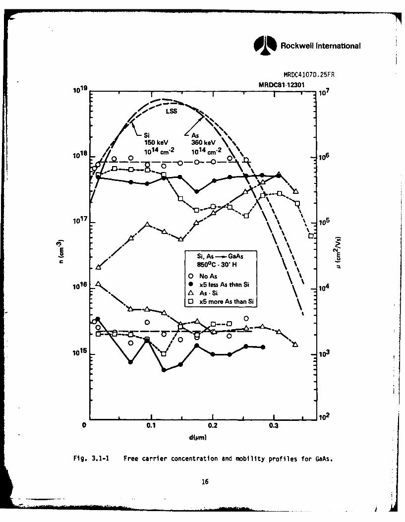
Fig. 3.1-1 Free carrier concentration and mobility profiles forGaAs ...................................................... 16
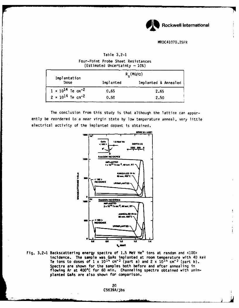
Fig. 3.2-1 Backscattering energy spectra of 1.5 MeV He+ ions at
random and <100> incidence. The sample was GaAsimplanted at room temperature with 40 keV Te ions todoses of 1 x 1014 cm "2 (part a) and 2 x 1014 cm"2
(part b). Spectra are shown for the samples bothbefore and after annealing in flowing Ar at 4000C for60 min. Channeling spectra obtained with unimplantedGaAs are also shown for comparison ........................ 20
Fig. 4.1-1 Distribution of FET threshold voltage observed in 55consecutively processed wafers over a 6 month period ...... 22
Fig. 4.1-2 Histogram of depletion voltages for a large number oftest chips from the same ingot, all processed inidentical ways over a period of 9 months .................. 24
Fig. 4.1-3 Histograms of depletion voltages for a number of testchips from a Bridgman and LEC ingot, respectively. Thetest chips were all processed simultaneously .............. 26
iitC5639A/sn
w . . .. . .. .. . . .. .. .. ... . . ... ..
Rockwell Intemational
MRDC41070.25FR
LIST OF FIGURES
Page
Fig. 4.1-4 Dependence of depletion voltage of Se channel implantson implant energy ......................................... 27
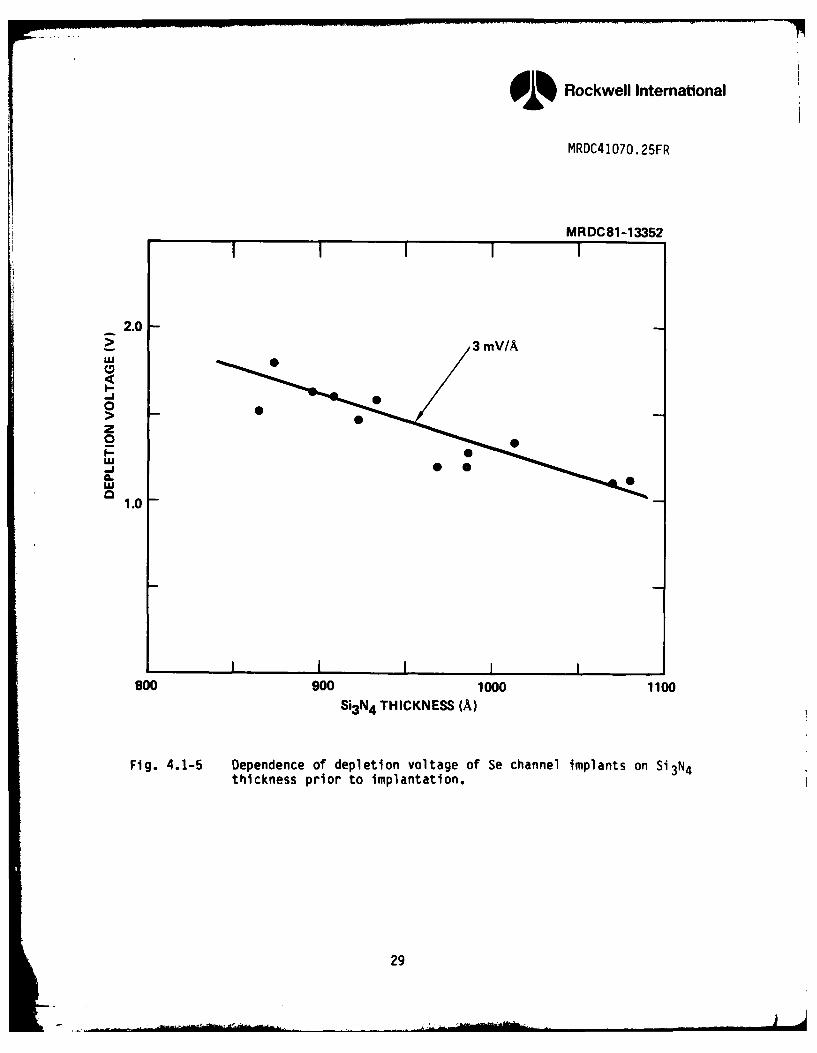
Fig. 4.1-5 Dependence of depletion voltage of Se channel implantson Si3N4 thickness prior to implantation .................. 29
Fig. 4.1-6 Dependence of depletion voltage of Se channel implantson Si3N4 thickness during anneal (for constant Si3N4thickness prior to implantation ........................... 30
Fig. 4.1-7 Depletion voltage of Se implanted wafers (at a dose of2.5 x 1012 ions/cm "2) as a function of the anneal time.The implants were made in semi-insulating GaAs substrates.The annealing cap consisted of sputtered Si3N4 ............ 33
Fig. 4.3-1 Schematic of second level interconnects yield teststructure ................................................. 41
Fig. 4.3-2 Photomicrograph of part of the second level interconnectsyield test structure ...................................... 42
Fig. 4.3-3 Yield of parallel second level metal lines fabricated usingseveral different metal deposition systems. The lineswere defined by ion milling ............................... 43
Fig. 4.3-4 Schematic of the cell used to build a long chain offirst/second level interconnects .......................... 45
Fig. 4.3-5 Portion of the long meander forming the interconnectintegrity test structure .................................. 46
Fig. 4.3-6 Yields of first/second level interconnects ................ 48
Fig. 4.4-1 Wafer map and histogram of test FET threshold voltages(-Vp) from a typical AR6 wafer ............................ 49
Fig. 4.4-2 Statistics of FET parameters from a typical AR6 wafer ..... 52
Fig. 4.4-3 History of average of threshold voltges, V., for the AR6wafers. Each data point represents the megn forone wa f er .. .. .. .. ... . . . . . . . . . . . . . . .. . . . 52
ivC5639A/sn
A )L Rockwell International
MRDC41070.25FR
LIST OF FIGURES
P age
Fig. 4.4-4 History of ohmic contact specific resistance for the AR6wafer. Each data point represents the mean for onewafer ..................................................... 53
Fig. 4.4-5 History of logic diode series resistance, Rs, for the AR6wafers. Each data point represents the mean for onewafer .................. 0...........0........................ 54
Fig. 4.5-1 Cross-section of the standard depletion mode GaAs MESFETused in SDFL logic ................................... . . 58
Fig. 4.5-2 Reliability of AuGe/Pt ohmic contacts with Schottkymetal overlay ............................................. 60
Fig. 4.5-3 I vs VP for all the 72 test FETs on a wafer atdifnerent stages of process and thermal treatment.a) After Schottky metalization; b) after second layermetalization; c) after aging for 2.5 hrs at 240*C, andd) after aging for 22 hrs at 240 0C ........................ 66
Fig. 4.5-4 History of ohmic contact resistance over a 12 monthperiod. Each data point corresponds to the mean for onewafer of a) total contact resistance; b) specificcontact resistance ....................... ........ ..... 69
Fig. 4.5-5 Oscillation frequency vs aging time for five 9-stage ringoscillators operating at 2000C. The frequencies arenormalized to the room temperature frequence at t = 0 ..... 72
Fig. 4.5-6 Oscillation frequency vs aging time for five 9-stage ringoscillators operating at 2500C. The frequencies arenormalized to the room temperature frequence at t = 0.The failure of one device was due to an instrumentationproblem .......... ......... 0......... .. .. . .. .. . ...... 73
Fig. 4.5-7 Arrhenlus plot for the medium lifetime of 9-stage ringoscillators. Failure was defined as the point when theoscillation frequency at the given temperature degradesby 20% .................................................... 74
vC5639Afsn
9 L Rockwell Intemational
MRDC41070 .25FR
LIST OF FIGURES
Page
Fig. 4.6-1 Photograph of the Censor SRA-100 DSW system ............... 76
Fig. 4.6-2 Characterization of the alignment accuracy of the Censorprojection aligner ........ .............. ...... ............. 77
Fig. 4.6-3 Censor SRA-100 resolution test results.................... 78
Fig. 4.6-4 Results of width measurement on metal lines fabricated bya plasma etched lift-off process .......................... 80
Fig. 4M6-5 Histogram of linewidth for metal lines of 1 pm nominalwidth .... ... .... ... ............... ....... 81
Fig. 4.6-6 Etch rates of Si02, Si, H2 and photoresist as a functionof H2 fraction ........ ...... 0........ . . . . . . . . . ... 82
Fig. 4.6-7 Uniformity of reactive ion etching (RIE).................. 84
Fig. 4.6-8 Uniformity of sputtered and chemical vapor deposited SiO 2across the diameter of a 3 inch wafer................... 85
Fig. 4.6-9 Uniformity of magnetron sputtered and E-beam evaporatedmetal layers across the diameter of a 3 inch wafer ........ 86
Fig. 4.7-1 Histogram of ohmic contact resistance across a 3 inchGaAs wafer ........ . . . . .. . . . . . .................. 88
Fig. 4.7-2 Wafer map and histogram of depletion voltages across a3 inch GaAs wafer. The depletion voltage is obtained byC-V profiling, and it is defined as the voltage corres-ponding to a 1015 cm" 3 carrier concentration........ ... 89
Fig. 4.7-3 Wafer map and histogram of FET threshold voltages for a3 inch diameter GaAs wafer... ..... ... .... ... 90
Fig. 4.7-4 Wafer map and histogram of FET saturation currents for a3 inch diameter GaAs wafer .............. oo ... . .. ...... 91
Fig. 4.7-5 History of mean threshold voltages of GaAs 3 inch wafers.. 92
viC5639A/sn
OD Rockwell International
MRDC41070.25FR
LIST OF FIGURES
Page
Fig. 4.7-6 Mean saturation current vs mean threshold voltag for50 pm wide test FETs on 3 inch GaAs wafers ................ 93
Fig. 5.1-1 Comparison of 1, 2 and 3 level SDFL gate configurations... 97
Fig. 5.1-2 Circuit diagram of simple SD2 FL logic gate ................ 98
Fig. 5.1-3 Logic diagram of 4 to 1 multiplexer realized with asingle SD.FL .. ................. 100
Fig. 5.1-4 Schematic of an improved version of the Schottky diode-diode FET logic (SD2FL) g ......................
Fig. 5.1-5 Photograph of the 8 x 8 bit parallel multiplier chip ...... 106
Fig. 5.1-6 Schematic of upper right corner (low order bits) of theSD2FL multiplier .......................................... 107
Fig. 5.2-1 Direct realization of the programmable shift register/pattern generator ......................................... 111
Fig. 5.2-2 Double-clocked OR/NAND master-slave flip-flop ............. 112
Fig. 5.2-3 Equivalent logic diagram of the 7-stage programmableshift register/pattern generator .......................... 113
Fig. 5.2-4 Equivalent logic diagram of the 8-stage programmableshift register/pattern generator .......................... 114
Fig. 5.2-5 Clock driver circuit for the programmable shift register/pattern generator ......................................... 116
Fig. 5.2-6 Photograph of the 7-stage and 8-stage patterngenerator chips ........................................... 117
Fig. 6.2-1 a) Schematic and logic diagram of a SDFL NOR gate.b) Logic diagram of a D type flip-flop built with NORgates ...................... . . . . . . . . . . . . ...... 125
Fig. 6.2-2 Logic diagram of a ripple type divide by four circuitformed by two cascaded D type flip-flops with a sourcefollower output driver .................................... 126
viiC5639A/sn
OD Rockwell International
MRDC41070.25FR
LIST OF FIGURES
Page
Fig. 6.2-3 Osclllograms showing long-term transients in a divideby four circuit. The radiation dose rate was 2 x 10¹⁰rads/s. The two traces in each oscillogram correspondto the output signal and the positive supply current, 1dd'respectively. The top figure corresponds to Vdd = 2.5 V,and the bottom figure to Vd = 3.0 V. The duration ofthe hash in the upper osci logram corresponds to therecovery time ............................................. 128
Fig. 6.2-4 Divide by four output (top) and clock input (bottom) inthe immediate vicinity of a 1.08 x 10¹⁰ rads/s radiationpulse. The control voltage V was adjusted to Vss =
0.75 V. The circuit performsp~he divide by four operationwi aout being interrupted by the radiation pulse .......... 129
Fig. 6.2-5 Maximum input clock frequency vs (Vpd - Vss) for divideby four circuits ........ ......................... ....... 132
I~~~~ Jv~~tii~
J_) t' i7 .'j ui i , -
Avail,Av 31ab ll 1 ij ,,-
Dist
viiiC5639A/sn
Rockwell International
MRDC41070.25FR
FOREWORD
The research covered in this report was carried out in a team effort
having the Rockwell International Microelectronics Research and Development
Center as the prime contractor with two universities and a crystal manufac-
turer as subcontractors. The effort was sponsored by the Defense Sciences
Office of the Defense Advanced Research Projects Agency and by the U.S. Army
Electronic Research and Development Command. The contract was monitored by
the Air Force Office of Scientific Research. The Rockwell program manager was
Fred H. Eisen. The principal investigators for each organization were:
Microelectronics Research and A. Firstenberg, R. Zucca
Development Center
California Institute of Technology M-A. Nicolet
North Carolina State University N.A. Masnari
Crystal Specialties W.P. Allred
Numerous other researchers were involved in the work reported herein. The
principal contributors were:
Microelectronics Research and P.M. Asbeck, A. Firstenberg,Development Center W.P. Fleming, D. Hou,
G.R. Kaelin, C.G. Kirkpatrick,C.P. Lee, F.S. Lee, M.J. Sheets,E.K. Shen, Y.D. Shen,J.D. Thompson, E.R. Walton,B.M. Welch, R. Zucca.
California Institute of Technology T. Banwelo, M. Martimaenpaa
North Carolina atate University J.R. Hauser, T.H. Glisson,R.J. Trew
Crystal Specialties J. Burns
ixC5639A/sn
9D Rockwell International
4 tVRDC417O.25FR
1.0 INTRODUCTION
This report covers a program on LSI/VLSI Ion Implanted Planar GaAs IC
Processing. As suggested by the title, the main objective of this program wasto realize the full potential of GaAs digital integrated circuits by expanding
and improving fabrication and material techniques. The principal goal was to
improve material and processing capabilities so that large wafers (over 3 inch
diameter) could be processed in order to satisfy anticipated needs for high-
speed low-power GaAs digital VLSI integrated circuits. In parallel with in-
creasing circuit complexity and wafer size, the program was also directed
toward an investigation of circuit reliability and the development of proces-
sing techniques capable of attaining the highest reliability. Circuit design
advancements were also planned, as well as MESFET device modeling. The pro-
gram also called for an investigation of radiation hardness of GaAs integrated
circuits. In the last semester of the program, a feasibility analysis of mask
programmnable logic arrays for high performance communication systems meeting
ERADCOM requirements was carried out. Three subcontractors, the California
Institute of Technology, North Carolina State University, and Crystal
Specialties, Inc. contributed to the program with their expertise in ion beam
techniques, device modeling, and crystal growth, respectively.
The highlight of the program was the successful implementation of theprocessing of 3 inch GaAs wafers, a capability which has not been emulated yet
by any other domestic or foreign laboratory. Parametric data from the 3 inch
wafers indicated significant improvement in process uniformity over the pre-vious 1 inch process. The mask set used to launch the 3 inch wafer process
contained 256 bit static RAMs, and the first successful operation of such a
chip was demonstrated on the early lots of 3 inch wafers.
This report contains a discussion of many activities related toGaAs IC processing, material, circuit design, modeling, and radiation
effects. Work at Crystal Specialties on growth of GaAs by the horizontal
Bridgman method, as well as comparisons between Bridgman and liquid encapsu-
1C5639A/jbs
9 Rockwell International
MRDC41070.25FR
lated Czochralski (LEC) material are discussed in Section 2.0. The work done
at the California Institute of Technology on dual implantations in GaAs and
low temperature annealing of GaAs implanted layers is covered in Section 3.0.
Section 4.0 contains the main topic of the program, IC processing. In addi-
tion to the development of the 3 inch wafer process, this section covers many
other aspects of processing such as control of FET threshold voltages, varia-
tions to the standard process, metallization yield, fabrication of 1 inch
wafers, and enhancements of circuit reliability from process improvements.
Circuit design and test is covered in Section 5.0. In this section the design
and test of a 8 x 8 bit parallel multiplier and of programmable shift regis-
ters/pattern generdtcv,, are discussed, as well as a feasibility study of mask
programmable logic arrays for applications which interest ERADCOM. Full de-
tails are presented in Appendix A. In Section 6.0 experiments to evaluate the
radiation hardness of GaAs digital integrated circuits are presented. Both
total dose and transient radiation sensitivity of the circuits are discussed.
Finally, in Section 7.0, the work done at North Carolina State University on
MESFET modeling is briefly summarized. More detailed information on this work
can be found in Appendix B.
2C5639A/jbs
Rockwell Intemational
MRDC41070.25FR
2.0 SEMI-INSULATING GaAs SUBSTRATE MATERIAL
Although the need for 3 inch diameter wafers makes the liquid encap-
sulated Czochralski (LEC) material the preferred one, the excellent quality of
this material was not clearly established at the beginning of this program.
Therefore, the growth of semi-insulating GaAs at Crystal Specialties by the
horizontal Bridgman (HB) technique started on a previous program was contin-
ued.1 This work is discussed in Section 2.1. Evaluation of HB material, and
of LEC material grown at Rockwell or purchased from commercial suppliers is
discussed in Section 2.2.
2.1 Growth of Semi-Insulating GaAs by the Horizontal Bridgman Method
Work at Crystal Specialties has resulted in the growth of several
large area single crystals of GaAs using the horizontal Bridgman technique.
(100) wafers cut from these crystals measured 2.5 in. wide and 4 in. long.
The crystals were grown in a quartz boat 1 in. deep, 2.5 in. wide and 4 in.
long. The seeds were oriented with the growth direction on the (110) axis so
that the (100) axis is in the vertical direction. By cutting the crystal
perpendicular to the vertical (100) axis, wafers as large as 2.5 x 4 in. could
be produced. Since cutting equipment large enough to slice this large area
was not available, the ingot was trimmed to about 2.5 x 3 in. before cutting.
Considerable progress has been made at Crystal Specialties in the
reduction of dislocations generated during crystal growth by the horizontal
Bridgman method. Single crystals with dislocation densities as low as 200
etch pits/cm 2 have been grown.
The crystals were grown in the (111) and (110) directions. The low
dislocations were obtained by close control of the thermal gradients and
arsenic pressure. Previously, the dislocation density of an ingot progres-
sively increased toward the tail of the ingot. Using these new techniques of
growth, the dislocations are considerably lower at the tail of the ingot.
Typically, ingots have dislocations which vary from about 5 x 10³ pits/cm 2 at
3C5639A/jbs
QRockwell International
MRDC41070. 25FR
the front of the ingot to about 1 x 10⁴ pits/cm3 at the tail. The new ingots
start at about 1 x 10³ pits/ cm2 3n the front of the ingot, and improve to a
value of about 200 pits/cm 2at the back end of the ingot.
It is evident from this work that very low dislocation density mate-
rial can be grown on a routine basis. Since twins and lineage arise from
dislocations, it appears that lowering dislocation densities may allow for
longer boats to be used without incurring in twinning and lineage problems.
This may lead to improvements in yield and lower cost of production.
2.2 Evaluation of HB and LEC Substrate Material
During the early phase of the program, when processing was done on
1-in, square wafers, integrated circuit fabrication was carried out with LEC
material on an experimental basis, while Bridgman-grown Cr-doped GaAs ingots
were providing a major fraction of the substrates processed. In order to in-
sure proper results in the IC fabrication process, qualification, testing and
preselection of ingots continued to be required. The selection was based on
(a) absence of thermal conversion during Si 3N4 capped anneals, and (b) proper
carrier density profiles obtained from representative Se implants. Of the 7
ingots grown by Crystal Specialties during the early phase of the program, 57%
tested. Of these, 4 proved to be qualified for ion-implantation in approximate
agreement with the previously observed long term yield. 1
A portion of the semi-insulating ingots grown by Crystal Specialtieswere supplied as rectangular slices with dimensions approximately 1.5 x 2 in.
grown in boats with square cross-section (rather than the customary semi-cylindrical cross-section). This technique, pioneered by Crystal Specialties,
represents a significant advance towards the development of GaAs slices of
large dimensions and standard shape (rectangular rather than round) as well as
standard size obtainable using boat growth techniques.
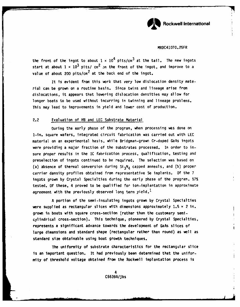
The uniformity of substrate characteristics for the rectangular slice
is an important question. It had previously been determined that the unifor-
mity of threshold voltage obtained from the Rockwell implantation process is
4C5639A/j bs
Rockwell International
MRDC41O7O.25FR
influenced by the particular substrate used.1 The substrate characteristics
are nonuniform principally because of spatial variations in the concentration
of Cr and residual impurities due to segregation effects during crystal
growth. The square wafers were tested for threshold voltage uniformity andcompared with the D shaped wafers. The results indicate that the uniformity
is different, but appears to be strongly ingot dependent.
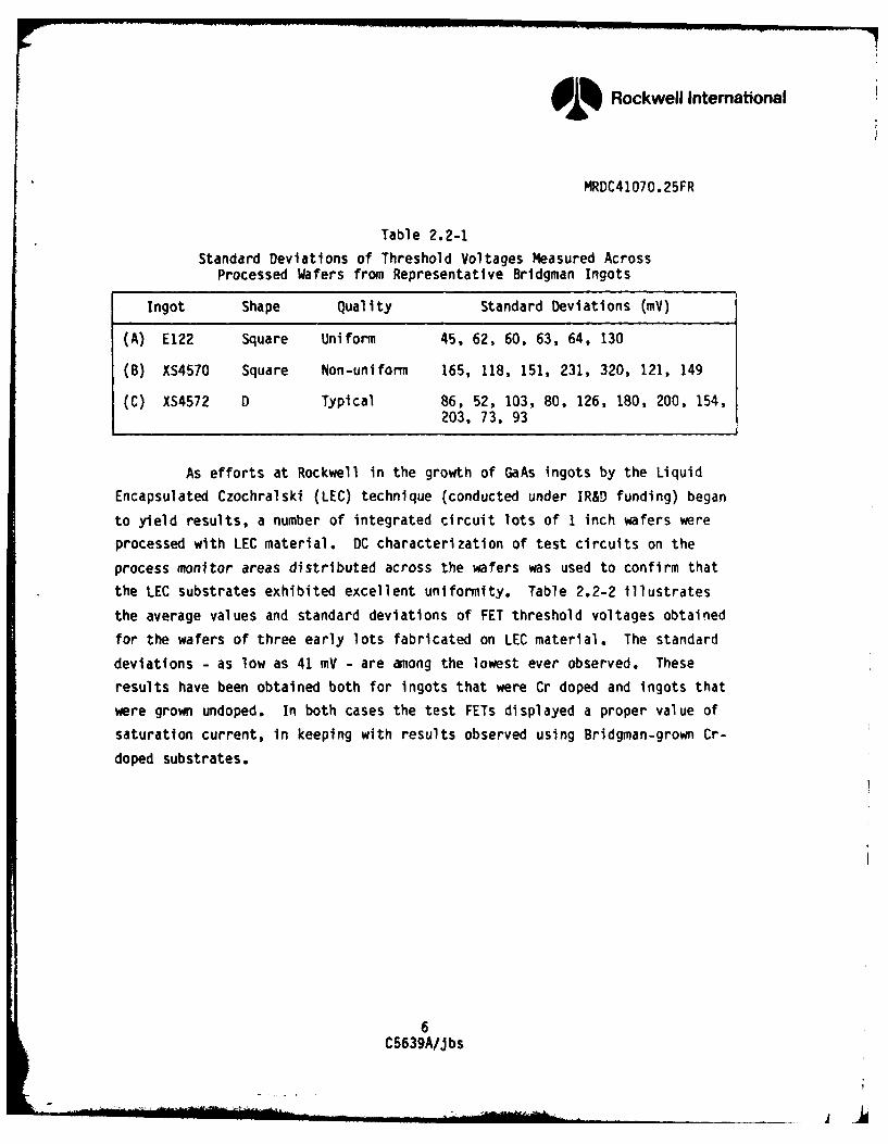
The substrate uniformity may be gauged by the standard deviation CTof threshold voltage among the test FETs fabricated on typical wafers. These
test FETs are part of the process monitor test areas included on all mask
sets, and are tested automatically for each wafer processed. The standard
deviations obtained correspond to the variations in doping encountered for the
Se implanted channel layer, over 24.5 x 24.5 mmi square wafers. Measured
values of av are shown in Table 2.2-1 for both a highly uniform square ingot
(ingot A) as well as for a square ingot of poor uniformity (ingot B). Values
obtained for a representative D shaped ingot are shown for comparison. Theseresults indicate that (a) the uniformity of threshold voltage is more stronglydominated by the substrate than the process, (b) the degree of uniformityachievable can be very high; (c) the results are ingot dependent in a way thatis not currently understood. The pattern corresponding to the variations in
threshold voltage is readily apparent in Fig. 2.1-1, which illustrates thedepletion voltages measured by the C-V technique on a highly nonuniform wafer
implanted with Se. A uniform gradient of depletion voltage is observed. The
magnitude of the gradient observed correlates very well with the measured
standard deviation of FET threshold voltage on processed wafers.
5C5639A/J bs
Rockwell International
MRDC41070.25FR
Table 2.2-1
Standard Deviations of Threshold Voltages Measured AcrossProcessed Wafers from Representative Bridgman Ingots
Ingot Shape Quality Standard Deviations (mV)
(A) E122 Square Uniform 45, 62, 60, 63, 64, 130
(8) XS4570 Square Non-uniform 165, 118, 151, 231, 320, 121, 149
(C) XS4572 D Typical 86, 52, 103, 80, 126, 180, 200, 154,203, 73, 93
As efforts at Rockwell in the growth of GaAs ingots by the Liquid
Encapsulated Czochralski (LEC) technique (conducted under IR&D funding) began
to yield results, a number of integrated circuit lots of 1 inch wafers were
processed with LEC material. DC characterization of test circuits on the
process monitor areas distributed across the wafers was used to confirm that
the LEC substrates exhibited excellent uniformity. Table 2.2-2 illustrates
the average values and standard deviations of FET threshold voltages obtained
for the wafers of three early lots fabricated on LEC material. The standard
deviations - as low as 41 mV - are among the lowest ever observed. These
results have been obtained both for ingots that were Cr doped and ingots that
were grown undoped. In both cases the test FETs displayed a proper value of
saturation current, in keeping with results observed using Bridgman-grown Cr-
doped substrates.
6C5639A/J bs
Rockwell International
MRDC41O7O. 25FR
> > > 'Lu N LU 0NC .
00 40r r=
S. 0
0 4WLU a LJ ~ J ~ L'
LU
4-' a'-4-' E
o .-
CLa
4-)(/ E
4a ) CU
a) C a
C EU >
LL
........- o
.. * .... 0
7)00
Rockwell International
MRDC4107O.25FR
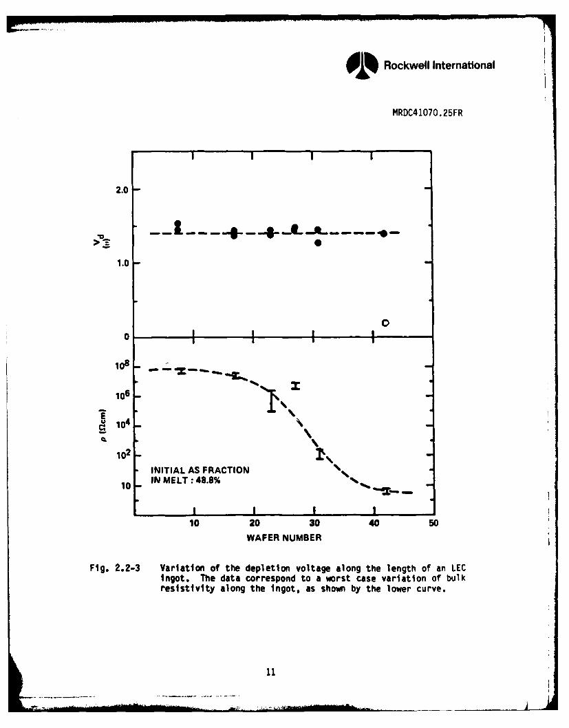
Table 2.2-2
Mean and Standard Deviation of FET Threshold VoltageMeasured on Wafers Processed with LEC Substrates
Lot Ingot V (V) av (mv)
AR4-8 R4 (Cr doped) 1.08 481.12 690.99 561.18 73
AR5-6 R5 (Cr doped) 0.99 621.26 411.18 64
AR5-8 R2 (undoped) 1.04 661.18 471.13 420.85 41
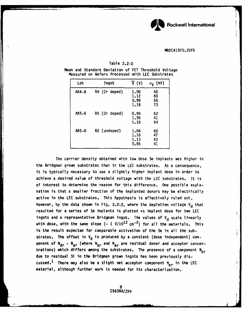
The carrier density obtained with low dose Se implants was higher in
the Bridgman grown substrates than in the LEC substrates. As a consequence,
it is typically necessary to use a slightly higher implant dose in order to
achieve a desired value of threshold voltage with the LEC substrates. It is
of interest to determine the reason for this difference. One possible expla-
nation is that a smaller fraction of the implanted donors may be electrically
active in the LEC substrates. This hypothesis is effectively ruled out,
however, by the data shown in Fig. 2.2-2, where the depletion voltage Vd that
resulted for a series of Se implants is plotted vs implant dose for two LEC
ingots and a representative Bridgman ingot. The values of Vd scale linearly
with dose, with the same slope (_ I V/10 1 2 cm"2) for all the materials. This
is the result expected for comparable activation of the Se in all the sub-
strates. The offset in Vd Is produced by a constant (dose independent) com-
ponent of Ndr - Nar (where Ndr and Nar are residual donor and acceptor concen-
trations) which differs among the substrates. The presence of a component Ndr
due to residual Si in the Bridgman grown ingots has been previously dis-
cussed.1 There may also be a slight net acceptor component Nar in the LEC
material, although further work is needed for its characterization.
8C5639A/Jbs
9D Rockwell International
MRDC4 1070. 25FR
a)q
04.) V) L
00
0 WV
C SV
W ..- -C -
IU 4.;fl
0a0.
CWL
. 4O)
C;
LL.
N (A)'PA
9
Rockwell International
MRDC41070,25FR
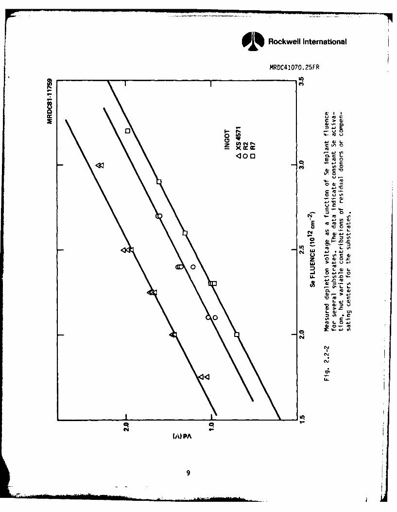
The uniformity of LEC grown ingots along their length is also a topic
of great interest. A measurement of the depletion voltage of Se Implanted
layers along the length of an LEC ingot was carried out and the results showed
excellent uniformity. For this study, test chips were cleaved from samplewafers selected along the length of an ingot, and subsequently capped, im-
planted with Se and annealed together in the standard fashion. The depletion
voltages, Vd, obtained for these test chips from C-V measurements are illus-
trated in Fig. 2.2-3. The excellent longitudinal uniformity is apparent in
the less than 100 mV variation from front to tail.
The ingot used in the uniformity test corresponds to a worst-case
study. In fact, for nearly all Rockwell-grown ingots measured, the bulk re-
sistivity is uniformly high (> 108 o/o) along the ingot length. On several
ingots, however, p-conductivity developed towards the tail region. The ingot
of Fig. 2.2-3 corresponds to such a case, as determined by resistivity mea-
surements of unannealed test chips, whose results are also shown in the
figure.
The fact that p-type conductivity occurs in unimplanted material
while no doping change occurs in Se-implanted layers is well explained by a
compensation model developed as part of Rockwell's IR&D effort. In the unim-
planted material, the carrier density is determined by the balance between
carbon acceptors (uniformly distributed along the ingot length) and EL2 deepdonors, whose concentration decrease along the ingot length because the mate-
rial became progressively enriched with Ga during crystal growth. In the im-
planted n-type material, however, the varying EL2 concentration has no effect
since these deep donors are neutral; the electron density is determined by the
balance beteen the (spatially uniform) Se donors and the (spatially uniform)
carbon acceptors.
As the program evolved, and encouraged by the good results obtained
from the LEC material, a full transition to LEC substrates was made, well in
time for the beginning of the processing of 3 inch wafers for which there is
no other alternative to LEC material. In addition to Rockwell, material
10C5639A/J bs
Rockwell International
MRDC41070.25FR
2.0
I- -- --4- _..L a._ - .
1.0
00
108
106 :
S1o4
102
INITIAL AS FRACTION
10 IN MELT : 48.8%
10 20 30 40 50WAFER NUMBER
Fig. 2.2-3 Variation of the depletion voltage along the length of an LECingot. The data correspond to a worst case variation of bulkresistivity along the ingot, as shown by the lower curve.
01 Rockwell International
MRDC41070.25FR
suppliers of LEC material have been monitored. Qualification studies on com-
mercial large diameter (3 inch) LEC GaAs materials produced by Cominco showed
that most of their ingots are suitable for integrated circuit processing.
Satisfactory resistivity after cap and anneal, and acceptable depletion volt-
ages were observed in several qualified crystals.
Wafer preparation was also evaluated. The supplier (Cominco) was co-
operative in realigning their flat system to provide for automatic crystallo-
graphic orientation of the large wafers coinciding with the flat orientation
system developed in the Rockwell LEC growth program. Edge beveling was not
yet available. Difficulties in polishing from the supplier still precluded
the purchase of polished wafers. Therefore, all the materials were being
bought as-cut for polishing at our facility. Figure 2.2-4 indicates the de-
gree of flatness typical of purchased materials. The numerous fringes indi-
cate a high center with several microns dropoff toward the edge. The Rockwell
polishing capability results in as few as 3-5 fringes on the same size su-
bstrate. Upgrades in polishing equipment are under way at several commercial
GaAs suppliers to improve their polishing results and significant improvements
are, therefore, expected in the near future.
12C5639A/J bs
Rockwell International
MRDC41O7O.25FR
MRDC82-18289
Fig. 2.2-4 Flatness photo of 3 inch polished GaAs wafer as received fromthe supplier. The wafer exhibits a high center.
13
Q% Rockwell International
MRDC41070.25FR
3.0 ION IMPLANTATION IN GaAs
The activities at the California Institute of Technology were di-
rected to the study of dual implantations of Si and As to determine whether it
is possible to obtain high activation for heavy n-type doping, an objective
that has eluded previous efforts. This work is discussed in Section 3.1.
Efforts were also directed toward the investigation of low temperature
annealing of implanted layers, which would provide many obvious advantages in
integrated circuit processing. This work is described in Section 3.2.
3.1 Dual Implantation of Si and As
Room temperature implanted Si is an excellent n-type dopant in GaAs,
generally producing a high degree of electrical activation for low-dose im-
plants. 2 However, an upper 2 x 1018 cm"3 limit apparently exists on the
achievable free electron concentration, attributed to the formation of neutral
Si-Si pairs,3 fixing the concentration for high-dose implantation. A series
of experiments exploring the potential advantages of dual implantation with a
complementary ion to enhance the Si electrical activation by maintaining local
stoichiometric balance has been carried out in close cooperation with the
Caltech group. These experiments have been completed and in summary, the re-
sults indicate that no increase in the upper limit of free carrier concen-
tration was observed, though a given level of activation was achieved at
reduced annealing temperatures.
Semi-insulating <100> Cr doped GaAs was implanted at room temperature
with 150 keY Si to doses of 1013, 1014 or 1015 ions/cm 2. Room temperature co-
implantations of 360 keV As were also made to doses either five times less,
equal to, or five times greater than the primary Si dose. The implanted sam-
ples were encapsulated with 2000 A of reactively sputtered S13N4 and annealed
at 850 or 9000C for 30 min in flowing hydrogen. All implanted and annealed
samples were characterized by sheet electrical measurements using a conven-
tional van der Pauw method. A standard anodic stripping technique was
employed for depth profiling of selected samples.4
14C5639A/Jbs
O l Rockwell International
MRDC41070.25FR
The effect of coimplanted As on the free electron concentration and
mobility profiles for samples implanted with 1014 Si cm- 2 and annealed at
850°C is shown as an example in Fig. 3.1-I. LSS profiles for the Si and
equal-dose As implantations are drawn for comparison. Arsenic has a pro-
nounced effect on the free electron concentration. The limitation of the free
electron concentration at _ 1018 cm-3 is evident in samples with little or no
As. The difference in the two profiles should be considered insignificant and
within experimental uncertainty. The integrated concentrations agree within
30% of the corresponding sheet values. An equal implantation of As at 1014
cm"2 reduces the free electron concentration near the surface by a factor of
25, and produces a large depth dependence. The mobility, in this case, shows
the same inverse correlation with the free carrier concentration as is ob-
served in bulk GaAs. With a large As dose, the free electron concentration
reaches the saturation level though there is a step at approximately Rp of the
LSS profile. The relative uncertainty of the points in the high As dose pro-
file is less than 25% for the first 2400A from the surface.
It is evident that enhanced Si substitutionality cannot be induced by
altering the local stoichiometry with coimplanted As at room temperature.
This result indicates that the threshold is not a function of compensating
species, but rather an intrinsic property of Si in GaAs.
Silicon diffusion is not an important parameter in this investigation
either. The profiles for single Si implantation extend to - 3.6 Rp for 1015
Si/cm "2 with 9000C annealing and to - 2.5 Rp for 1014 Si/cm "2 with 850°C
annealing. It is evident from the profiles in Fig. 3.1-1 that As does not
significantly influence Si redistribution.
The morphology of GaAs preceding annealing does not appear to be a
factor restricting enhanced substitutionality. Extrapolation of results for
the amorphization of GaAs by implanted Si, as established by Grimaldi et al
using channeling, 5 indicate that GaAs is fully amorphous to a depth of -2 Rp
after room temperature implantation of 1015 Si/cm "2. The subsequent As im-
plantation into the amorphized layer is thought to merely extend the amorphous
15C5639A/jbs
Rockwell International
MRDC41070.25FR
1019 MRDC81-12301
LSS
150 keV 360 keV \ ,/ " 1014 cm-2 1014 cm-2 X% \
Iola 106
0: 01017 \ 10
Si, As *GaAs \ EC 850 0C- 30 H :.
O No As1016 0 x5 less As than Si 4
A As-Si 10
0 x5 more As than Si
00
0 0.1 0.2 0.3
d(pm)
Fig. 3.1-1 Free carrier concentration and mobility profiles for GaAs.
16
TA
9 Rockwell Intemational
MRIDC41070,25FR
region. In previous work it was shown for single specie implantation that
regrowth is primarily governed by the initial amorphous thickness, irrespec-
tive of ion specie or dose. It therefore seems likely that the residual dam-
age is qualitatively the same for all samples coimplanted with 1015 Si/cm "2 .
Thus, regrowth of GaAs from the amorphous state is not a sufficient condition
at high doses for As to enhance Si activation. In contrast, the implantation
of 1013 cm"2 150 keV Si leaves the GaAs polycrystalline. Extrapolation of
results for the amorphization of GaAs by implanted As indicates that an amor-
phous layer may have been produced by implanting 101 3 or 5 x 1013 cm"2 360 keV
As, though good regrowth is expected upon annealing because the amorphous
layer would have had to be thin (< 500A). There was certainly no amorphous
layer after a 0.2 x 101 3 360 keV As implantation. It is therefore apparent
that to maintain a crystalline structure is not a sufficient condition for
enhanced activation with As either.
The electrical profiles for 1014 Si/cm -2 (Fig. 3.1-1) suggest that
substrate morphology is a factor governing Si activation. In contrast to the
behavior shown for 1013 and 1015 Si/cm "2, coimplanted As has a strong influ-
ence on the Si activity at 1014 cm"2. Note that this dose coincides with the
transition region between the formation of a damaged single crystalline layer
and the full amorphization of GaAs by room temperature implantation of Ar, As,
S or Si in the energy range of hundreds of KeV. The As dose dependence ob-
served in Fig. 3.1-1 most probably arises from an explicit dependence of the
residual damage on the As dose in that transition region. The pronounced de-
crease in free electron concentration at the surface with 1014 As/cm "2 implan-
tation is probably due to incomplete annealing. Sheet measurements (Fig.
3.1-1) show that the effect of As is less pronounced at 9000C than at 8500C.
This further substantiates the conclusion that the effects seen in Fig. 3.1-1
are structural in origin. Since compensation by Cr gettering at the surface
is not observed at other doses, Cr compensation is not a likely cause here
either. Extrapolation of amorphizatlon ranges reported for As in GaAs indi-
cate that at 5 x 1014 cm-2 360 keV As will produce a fully amporphous region
extending to 1-2 Rp. The recovery of the free electron concentration observed
17C5639A/Jbs
01 Rockwell International
MRDC41070.25FR
with 5 x 1014 cm-2 As implantation could therefore be attributed to regrowth
from the amorphous state. Whatever the actual causes may be, it is evident
that a rigorous characterization of the annealed layer in this transition
region would require careful structural investigation of each particular case.
In conclusion, no indication has been found that Si substitutionality
in GaAs can be enhanced by complementary dual implantations at room tempera-
ture. The 2 x 1018 cm" 3 free electron limit for Si in GaAs does not appear to
be associated with local stoichiometry or regrowth conditions. Coimplanted As
does not have a perceptible effect on Si activation except in the transition
region of - 1014 Si/cm "2 , where a complete annealing is delayed and a complex
behavior is observed.
3.2 Low Temperature Annealing of Implanted Layers in GaAs
Room temperature implantation and low temperature (< 6000C) regrowth
have been subjects of investigation at Caltech and several other laboratories
recently.6 " 10 The main motivation for this work has been the hope of simpli-
fying the process of electrical activation of ion implants into GaAs, and the
wish to explore crystal regrowth properties in 3-5 compounds. In recent
studies6 it was shown that <100> GaAs that has been amorphized to a depth of
< 400A by implantation can regrow at 4000C with a crystal quality that appears
from spectra of channeled He backscattering to be almost as good as that of
virgin material. More recently, the regrowth process for shallow implantations
of dopant Te ions. has been explored. Te was chosen 1) because it is a well
known n-type dopant in GaAs, and 2) because Te2+ molecules can readily be
formed by ionization of Te vapor, facilitating low energy implantations. The
question addressed was whether electrical activation could be achieved by low-
temperature regrowth of shallow amorphized GaAs layers.
Semi-Insulating <100> wafers of Cr-doped GaAs were implanted at room
temperature with 80 keV Te2+ molecules to doses of 1 x 10¹⁴ and 2 x 10¹⁴ atoms
cm 2. According to the tabulations of Gibbons et al., 11 40 keV incident Te
atoms should have a projected range in GaAs of 144A, with a standard deviation
18C5639A/Jbs
___
9 Rockwell International
MRDC41070.25FR
of 63A. Annealing was conducted at 4000C in flowing dry argon for 60 min.
Since the regrowth rate of <100> GaAs at this temperature is known to be at
least 130A min - 1, it is expected that all possible regrowth must have been
completed in this time. Backscattering analysis was conducted with a 1.5 MeV
incident He+ beam channeled along the <100> direction. A glancing exit geom-
etry (scattering angle = 980) was used to increase the depth resolution.
The spectra from the sample implanted to a dose of 1 x 1014 cm-2 are
shwon in Fig. 3.2-la, together with a spectrum for a channeled incident beam
from an unimplanted GaAs sample. It is evident that the implantation created
an amorphous layer with a thickness of - 500A. One can also see that the
annealing resulted in good regrowth of this layer back to the sample sur-
face. The spectrum for channeling incidence deviates only slightly from that
obtained with virgin material, viz. a slightly larger surface peak caused by
greater surface disorder and slightly greater dechanneling. Similar spectra
are shwon for the implantation to a dose of 2 x 1014 cm"2 in Fig. 3.2-1b.
Here the initial amorphous thickness is - 600A, and again the backscattering
spectrum with the channeled beam indicates excellent regrowth, the beam
sensing only a low concentration of added defects. For both implantation
doses, the abundance of Te atoms was too low for the Te signal in the back-
scattering spectra to be discerned in a statistically significant manner.
Sheet resistance measurements were performed on the samples by the
van der Pauw method both before and after furnace annealing. The results are
shown in Table 3.2-1. The values are high after implantation, but increase
even further as a result of the annealing. Such an increase of resistance has
been observed previously for GaAs implanted with either donor or acceptor
ions 1 2'13 and more recently by Kular et al. 7 The conductivity after implanta-
tion has been interpreted as a thermally assisted hopping process associated
with localized states within the forbidden gap. 12 Low temperature annealing
is believed to slightly order the material decreasing the number of localized
states and increasing the room temperature resistivity.7
19C5639A/J bs
Rockwell International
MRDC4107 . 25FR
Table 3.2-1
Four-Point Probe Sheet Resistances(Estimated Uncertainty -10%)
ImplantationR MQO
Dose Implanted Implanted & Annealed
1 x 10¹⁴ Te cm-2 0.65 2.65
2 x 10¹⁴ Te cm-2 0.50 2.50
The conclusion from this study is that although the lattice can appar-
ently be reordered to a near virgin state by low temperature anneal, very little
electrical activity of the implanted dopant is obtained.
< IGOU>D SI-1
RANDOM TEANAE
INCI At
T *t01
t. 2 40 eV * "T
INIDCK UNANEDED A
10 DNINCIDEN
IMLANTED2. 4 -1* 40 h8Y. "fANNEALED IN Ar
300kALMAC
UNM r NT
U U II IA
Fig. 3.2-1 Backscatterlng energy spectra of 1.5 14eV He* ions at random and <100>incidence. The sample was GaAs implanted at room temperature with 40 keVTo ions to doses of 1 x 10¹⁴ CM-2 (part a) and 2 x 10¹⁴ CM-2 (part b).Spectra are shown for the samples both before and after annealing inflowing Ar at 4000C for 60 min. Channeling spectra obtained with unim-planted GaAs are also shown for comparison.
20C5639A/J bs
9Rockwell International
MRDC41O7 . 25FR
4.0 INTEGRATED CIRCUIT PROCESS DEVELOPMENT
One of the main accomplishments of the program was the implementationof the processing of GaAs digital integrated circuits on 3 inch diameter
GaAs wafers. This subject is discussed in Sections 4.6 and 4.7. Several
other aspects of the process technology from control of FET threshold voltage
to improvements in process leading to higher reliability are covered in
sections, 4.1 through 4.5.
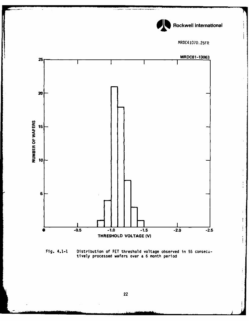
4.1 Reproducibility of FET Threshold Voltage
The control and reproducibility of the electrical characteristics ofthe FET channel implant are critical concerns for high yield fabrication ofIC's. The channel (n-) implant determines the threshold voltage for switching
of the logic gates, and this voltage must be tightly controlled particularly
for low voltage, low power IC's.
The technological development and investigation of the n- implantshas been an ongoing activity at Rockwell. Significant progress has been
achieved, and for a statistically significant period of time, reproducibilityhas been satisfactory for high yield fabrication of high speed low power SDFL
circuits. This result is evident in the data of Fig. 4.1-1, which show the
distributions of threshold voltage obtained on all the 1 inch wafers processed
throughout a period of over 6 months. The results were obtained by automated
probing of 1 pmn gate FETs distributed across the processed wafers. A histo-gram (Fig. 4.1-1) was made for the average threshold voltages obtained from
each wafer. The overall average threshold voltage was 1.12 V (as desired forlow-power, high speed depletion t4ESFET devices), while the standard deviation
Of VT in Fig. 4.1-1 was 110 mV, well within the range required for SDFL cir-cuits. The results include 55 consecutively processed wafers, corresponding
to 14 lots and 8 different GaAs substrate ingots. Most of the wafers corres-pond to Bridgman grown substrates (5 ingots), although the Rockwell grown LEC
substrate materials are also represeneted (3 ingots). Comparable control over
21C5639A/Jbsj
9 Rockwell International
MRDC41070.25FR
25 MRDC81-13063
20-
CLu 15 -U-
U-0U
.IGz 10 -
5-
0 -0.5 -1.0 -1.5 -2.0 -2.5THRESHOLD VOLTAGE (V)
Fig. 4.1-1 Distribution of FET threshold voltage observed in 55 consecu-tively processed wafers over a 6 month period
22

Rockwell International
MRDC41070.25FR
VT have been obtained for both types of substrates, provided ingot qualifica-
tion tests are used for material selection, and implant fluences for IC wafer
lots are chosen on the basis of test results with similar material. However,
on the basis of a fixed implant dose, unselected ingot process, the LEC
materials display significantly better reproducibility.
Data on uniformity of VT across the wafers have similary been good
over an extended time. For the same 6 month period, the median standard
deviation of VT across the 1 inch wafers has been only 64 mV. The uniformity
of the LEC grown substrates has been significantly better (median standard
deviation of VT of 55 mV) than that for Bridgman substrates (median standard
deviation of 84 mV). The superior unfiormity is expected on the basis of the
improved purity of the LEC material, as well as its growth size and geometry
which are better adapted to decrease the effects of impurity segregation
during crystal growth.
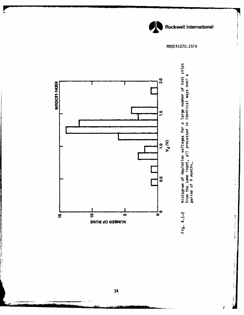
A long-standing problem with the investigation of factors which
influence the reproducibility of ion implanted layers has been the difficulty
of distinguishing implant variations that are due to process differences, from
implant variations due to differences between substrate material properties.
Therefore, data have been accumulated to separate the individual contributions
of these two effects.
In order to observe the magnitude of the process-related variations
alone, a test chip from a fixed control ingot was included in each of 47 dif-
ferent implant runs carried out over a period of 9 months. The test chips
were processed in a nominally identical way (with, for example, nominally
identical S13N4 encapsulant thickness and implant dose). Measurements of the
depletion voltage Vd (voltage necessary to deplete the carrier density to 1016
cm"3) yielded the results shown in Fig. 4.1-2. The standard deviation of Vd
over this distribution was found to be 153 mV (after excluding 12% of the runs
which yielded anomalously low activation, probably related to contamination
effects).
23C5639A/jbs
Rockwell International
MRDC41070. 25FR
.
E
0) a)> m
'41
L
C;V
q ~. 4JI- '
SNnu: :10 uIswINI'N.
24
" • .. ., i J *.. .. .V 0
I E0)
Rockwell International
MRDC41O70.25FR
In order to determine the variations in implant results that are re-
lated to substrate material alone, an experiment was conducted in which test
chips from a number of different ingots were processed simultaneously. Twelve
Bridgman ingots (obtained from Crystal Specialties and Mitsubishi-Monsanto)
were represented, as well as twelve LEC ingots (grown at Rockwell). The
ingots were preselected according to the standard qualification tests. The
distribution of depletion voltage Vd shown in Fig. 4.1-3 was obtained. For
the Bridgman materials the standard deviation of Vd was 304 mV (after exclud-
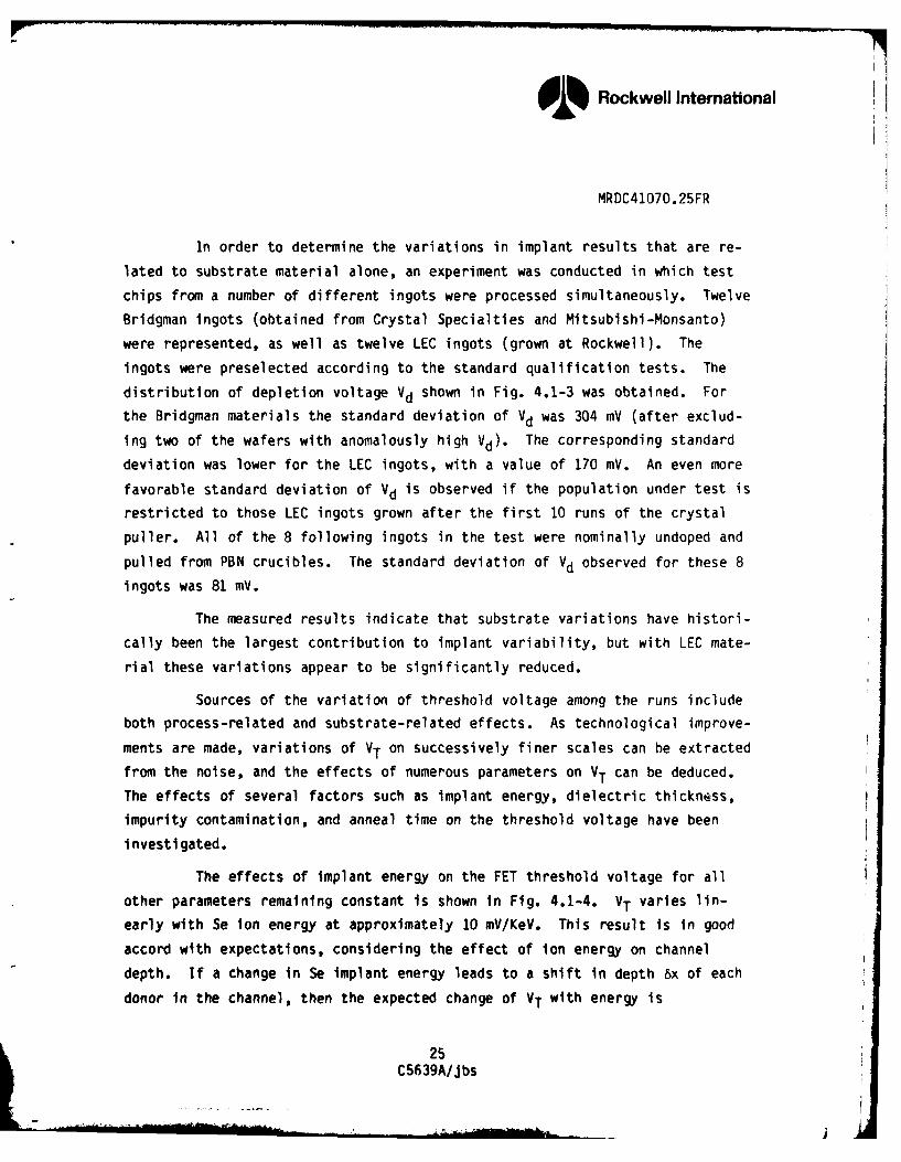
ing two of the wafers with anomalously high Vd). The corresponding standard
deviation was lower for the LEC ingots, with a value of 170 mV. An even more
favorable standard deviation Of Vd is observed if the population under test is
restricted to those LEC ingots grown after the first 10 runs of the crystal
puller. All of the 8 following ingots in the test were nominally undoped and
pulled from PBN crucibles. The standard deviation of Vd observed for these 8
ingots was 81 mV.
The measured results indicate that substrate variations have histori-
cally been the largest contribution to implant variability, but with LEC mate-
rial these variations appear to be significantly reduced.
Sources of the variation of threshold voltage among the runs includeboth process-related and substrate-related effects. As technological improve-
ments are made, variations Of VT on successively finer scales can be extracted
from the noise, and the effects of numerous parameters on VT can be deduced.
The effects of several factors such as implant energy, dielectric thickness,
impurity contamination, and anneal time on the threshold voltage have been
investigated.
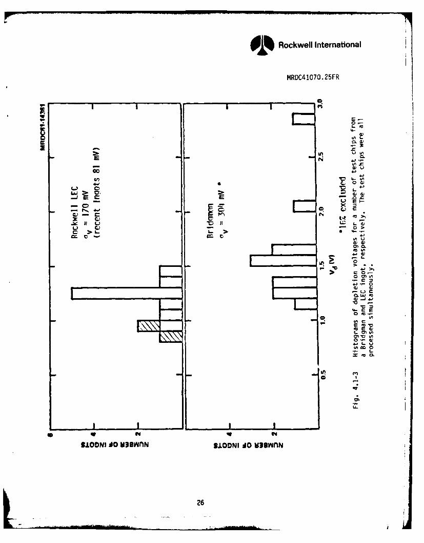
The effects of implant energy on the FET threshold voltage for all
other parameters remaining constant is shown in Fig. 4.1-4. VT varies lin-
early with Se ion energy at approximately 10 mV/KeV. This result is in good
accord with expectations, considering the effect of ion energy on channel
depth. If a change in Se implant energy leads to a shift in depth bx of each
donor in the channel, then the expected change of VT with energy is
25C5639A/Jbs
9Rockwell International
MROC4 1070. 25FR
4--1
W 4 J
a 4
4-
UU4- SC . 4)
2 4-
cc 0
LCL
C,-
4) 4)
SIODNI~ ~~~~ C.. C~wNSON 0M9n
26J E
Rockwell International
MRDC4 1070. 25FR
MRDC81-130646I
Se2.3 E 12er 2
Si3 N4 950A
2.0-
'U
0I--J
W 1.0-
'U
300 350 400IMPLANT ENERGY (KeV)
Fig. 4.1-4 Dependence of depletion voltage of Se channel implants on im-plant energy.
27
' Rockwell International
MRDC41070.25FR
SVT VT 8x _ 6x (1)
6E 6x 6E e implant 6E
Here €implant is the total implant dose and 6x/6E is the total stopping power
of GaAs for Se ions. Using 0implant = 2.3 x 1-12 cm- 2 and a stopping power of
3.45A/KeV as given by Gibbons et al, 11 the predicted change is 11.4 mV/KeV, in
good agreement with experiment. A similar effect is expected for variations
in Si3N4 cap thickness since in the Rockwell process the cap is deposited
prior to implantation. If the stopping power of Si3N4 and GaAs are con-
sidered to be equal, then the predicted change of VT with cap thickness is
3.3 mV/A. This result is again in good accord with experiment, (approximately
3 mV/A) as shown in Fig. 4.1-5.
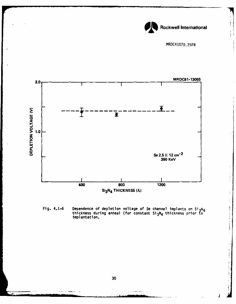
The stress produced by the Si3N4 cap has been a subject of concern
for some time. However, recent measurements indicate that changes in cap
stress do nto cause variations in VT. This result is inherent in the above
results where the cap thickness was varied prior to implantation, since the
stress imparted to the GaAs surface is directly proportional to cap thick-
ness. To examine this effect further, a series of samples were capped and
implanted, and then the cap was thinned substantially (after implantation).
As shown in Fig. 4.1-6, the measured VT for these samples was constant, even
though the cap-induced stress varied by up to a factor of 3.
To study the effects of Au, Cu, Ni, Ti contamination, evaporated
layers of these metals were deposited on the back sides of test wafers of
semi-insulating GaAs. The wafers had been previously encapsulated with sput-
tered Si3N4 , and implanted with Se (at a fluence of 2.5 x 1012 cm2 , typical of
FET channel layers). The wafers were subsequently annealed at 8500C for 30
min, as used in the IC process. Sealed quarz ampoules were utilized to avoid
furnace contamination. After stripping the dielectric encapsulant and car-
rying out C-V measurements, it was found that the Ni and Ti contaminated sam-
ples were comparable to concurrently processed uncontaminated control wafers
(having a threshold voltage of -2.0 1 0.1 V), while there was no discernable
implant activation in the Au or Cu contaminated samples. It was of interest
28
C5639A/j bs
Q % Rockwell International
MRDC41O7O. 25FR
MR DC81-13352
2.0
0
z0PJ 0
9L
1.0
Boo 900 1000 1100S13 N4 THICKNESS (A)
Fig. 4.1-5 Dependence of depletion voltage of Se channel implants on S13N4thickness prior to implantation.
29
Rockwell International
MRDC41070.25FR
2.0 MRDC81-13065
LU
> 10I-.J
• 1.0z0LUA.LU
Se 2.5 E 12 cm- 2
390 KeV
SI I400 800 1200
Si3 N4 THICKNESS (A)
Fig. 4.1-6 Dependence of depletion voltage of Se channel implants on Si Nthickness during anneal (for constant S13N4 thickness prior toimpl ant at i on.
30
Rockwell International
MRDC41070.25FR
to determine if the effects of Au and Cu could be eliminated by protecting the
back sides of the wafers with sputtered silicon nitride. Accordingly, samples
were processed with evaporated metal layers on the back of wafers encapsulated
both front and back. Again, no implant activation was obtained. Apparently
these metals can readily diffuse through the cap.
Investigation of silicon contamination of the cap-GaAs interface was
undertaken because of the concern that free Si-rich silicon nitride could po-
tentially be formed in the early phases of the cap sputter deposition under
some circumstances. To investigate its effects, a silicon layer of the order
of 15A thick was intentionally deposited on test GaAs wafers, and followed by
immediate deposition of the standard Si3N4 cap without exposing the wafers to
air. The silicon deposition was accomplished by sputtering, using a silicon
target and argon plasma; a nitrogen plasma was subsequently used to produce
the Si3N4. The contaminated wafers were implanted with Se, annealed and eval-
uated in the standard fashion. It was anticipated that an extra donor com-
ponent would appear due to silicon indiffusion. Unexpectedly, the profiles
showed that in addition to the normal Se donor concentration, there was an
acceptor-like doping component localized near the GaAs surface, as determined
from a reduction in the absolute value of the threshold voltage of about
0.7 V, and an increase in the zero-bias depletion depth of about 600A. The
nature of the acceptor is not known. It may result from an alteration of the
GaAs stoichiometry near the surface, if Ga or As preferentially interacts with
the silicon-rich interfacial layer.
Variations of depletion voltage with the anneal time were also in-
vestigated. Test chips of Cr doped or undoped semi-insulating GaAs were
capped, Se-implanted and then annealed for varying periods of time at 8500C.
C-V measurements were then done to determine carrier profiles and depletion
voltages, Vd. The carrier profiles for long anneal times showed increase
depth and lower peak carrier densities compared with the standard 30 minutes
as qualitatively expected for Se diffusion.
31C5639A/Jbs
V Rockwell International
MRDC41070.25FR
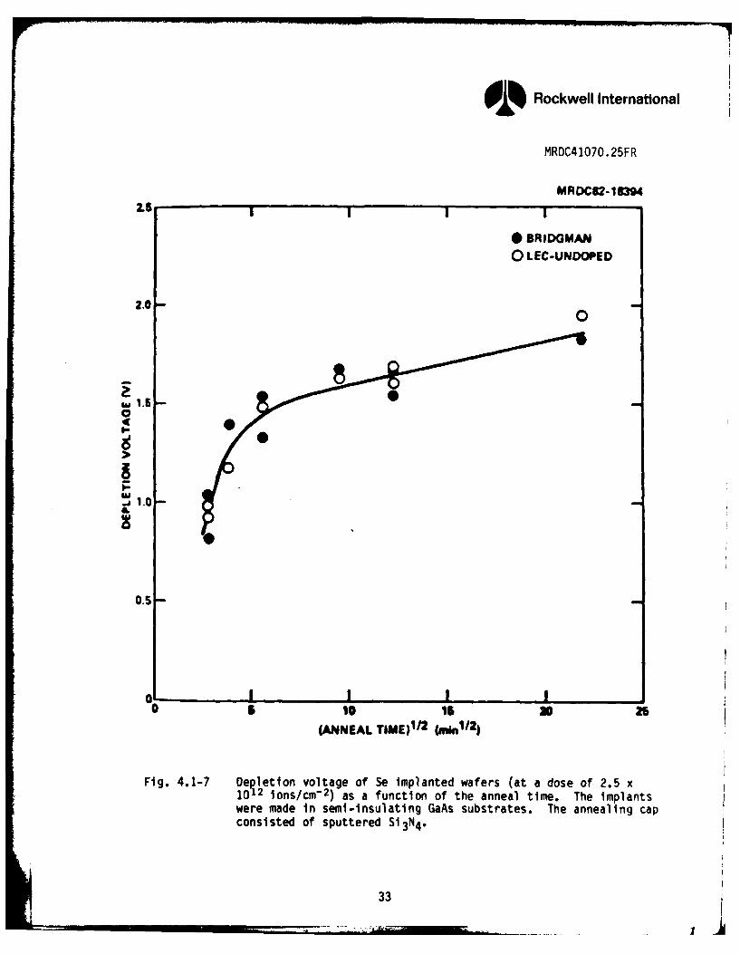
Significant activation was found for anneals as short as 8 minutes.
The variation of Vd with anneal time is shown in Fig. 4.1-7. It is apparent
that Vd is quite sensitive to the time in the range below 30 minutes, suggest-
ing that the current process represents a good compromise between limiting
diffusion and avoiding significant Vd variations. No significant difference
was found between the behavior of Cr doped and undoped LEC substrates, indi-
cating that the changes in Vd from Cr diffusion occur rapidly (in less than 5
minutes), and then saturate due to Cr depletion, so that further changes are
apparently related only to Se diffusion.
4.2 Evaluation of a 3-Implant Process
Two implantations are normally used in the Rockwell fabrication proc-
ess for digital IC's. One implant (called n-) is used to form the FET chan-
nels, and the other (called n+ ) to form the cathodes of the logic diodes. Both
implants are superimposed in ohmic contact regions to obtain low sheet resis-
tance in those areas. Since implantations are done prior to any other fabri-
cation step, there is no obstacle to using more than two implants. Experi-
ments were undertaken to determine whether an additional implant (called n++)
in the ohmic contact regions might lower the contact resistance.
In this experiment, silicon used for both the n+ (second) and n++
(third) implant in order to avoid mixing of implant species and recognizing
that silicon implants result in high electrical activations. 14 Processing
proceeded in a normal manner with the addition of the higher dose silicon
implant ranging from 3.8 x 1012 cm-2 to 1014 cm"2 . This implant was masked
using the ohmic contact mask, therefore allowing only the local regions under
the ohmic contacts to be heavier doped. One-inch square wafers were implanted
with various doses over 4 quadrants so that variations of contact resistance
could be compared with variations of sheet resistance on the same wafer.
The additional n++ implant processing was conducted without diffi-
culty. This indicates that implants through the cap (Si3N4) up to doses of
1014 cm"2 can be accomplished without any detrimental effects resulting from
32C5639A/Jbs
Rockwell International
MRDC4 1070. 25FR
MRDC82-ISM92.isI
* BRIDGMANo LEC-UNdDOPED
2.0-
,1.5
0.5
OL010 0 0
"NA I-)/ (ii2
i g.417 Dpeinvlaeo eipatdwfr a oeo .101 iosC-)a tuctoOfteana tm. Teipatweemd nsm-nuaigGa usrts h neln a
0.sse5o pterdS34
I I I33
Rockwell International
MRDC41070.25FR
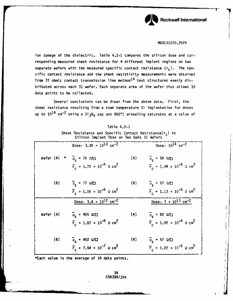
ion damage of the dielectric. Table 4.2-1 compares the silicon dose and cor-
responding measured sheet resistance for 4 different implant regions on two
separate wafers with the measured specific contact resistance (rc). The spe-
cific contact resistance and the sheet resistivity measurements were obtained
from 72 ohmic contact transmission line method 14 test structures evenly dis-
tributed across each IC wafer. Each separate area of the wafer thus allows 18
data points to be collected.
Several conclusions can be drawn from the above data. First, the
sheet resistance resulting from a room temperature Si implantation for doses
up to 1014 cm"2 using a Si3N4 cap and 8500C arnealing saturates at a value of
Table 4.2-1
Sheet Resistance and Specific Contact Resistance(rc) vsSilicon Implant Dose on Two GaAs IC Wafers
Dose: 3.38 x 1013 cm- 2 Dose: 1014 cm-2
Wafer (A) * p5 =76 9/0 (A) Ps 58 Q/01 6 c 2 0-6 m2
rc =1.72 x 1 cm2 rc : 1.94 x 10 Qcm
(B) Ps 77 Q/] (B) s =57 Q/010- 6 c 2 10c- 6 c 2
= 1.16 x 10 rc- = 1.13 x10 cm
Dose: 3.8 x 1012 cm-2 Dose: 7 x 101 3 cm- 2
Wafer (A) Ps = 455 Q/ (A) s= 62 Q/0
rc = 1.87 x 10- Q cm2 c =.2 x 10-6 cm2
(B) P = 452 1O (R) = 57 Q/O
rc =7.94 x 10 g cm c =1.22 x10- Qcm
*Each value is the average of 18 data points.
34C5639A/Jbs
• i
Rockwell International
MRDC41070.25FR
60 Q/o. It is estimated from earlier Si implantation profile studies that a
peak carrier concentration of _ 1018 cm"3 can be expected from this process.
It is well known from past work that Si implant activation levels go down with
increasing implant dose, and that continuing to increase the dose does not
necessarily result in higher levels of carrier concentrations with the present
cap and anneal conditions. Thus, it is not surprising that a dose of 7 x 10¹³
cm-2 resulted in a similar sheet resistance (- 60 9/0) as a 1014 cm-2 dose.
Even the 3.38 x 1013 cm-2 dose level yields a respectable 76 -77 9/0 sheet re-
sistance. In general, the lowest ps values observed using this process at
this laboratory has been - 40 P/o for higher doses and higher anneal tempera-
tures (9000 C). A dose of 3.8 x 1012 cm-2 (- 450 9/O) was included in these
experiments to simulate the normal implant dose conditions used in the current
process to compare with the higher doping levels under investigation. In all
of the implant regions the average value of rc was measured to be
_ I x 10-6 g * cm2. The specific contact resistance measurements on these
wafers clearly indicate that using a high quality ohmic contact process over a
sheet resistance range of 60-450 9/0 results, at least initially (as proc-
essed) in similar ohmic contact resistance.
The experiment on a third, n++, implant was completed by observing
the correlation between circuit switching speed and doping density under ohmic
contact regions. Nine-stage ring oscillators were fabricated on the wafer
that was partitioned in four quarters, with each quarter of the wafer receiv-
ing separate n+ + Si implantation doses. The data presented in Table 4.2-2
represent a summary of ring oscillator performance for these four different
areas. It can be seen that the frequency of operation increases when the
sheet resistance is decreased. A range of ps from 57 to 453 Q9/j results in
maximum oscillation frequencies of 360 MHz ( = 154 ps) and 255 MHz (=
218 ps), respectively. The overall ring oscillation speeds are very modest
due to the exceptionally low threshold voltage MESFETs used in this experi-
ment. However, propagation delays in the 150-200 ps region are quite good
considering the associated low power dissipation, providing speed-power prod-
ucts of 24-27 fJ. The scaling of propagation delay with n++ doping level will
35C5639A/jbs
Rockwell International
MRDC41070.25FR
more strongly dominate in a circuit employing low threshold MESFETs circuit
( O.6V) such as the one tested, as opposed to the more typical, - 1.0 V,
MESFETs thresholds used for SDFL. This is because reducing source resistance
is comparatively more important in MESFET devices with higher channel sheet
resistances.
Table 4.2-2
Ring Oscillator Performance vsSheet Resistance in the Ohmic Contact Region
Wafer Gate Parameters
Location ps(9/O) *f(MHz) r(ps) P(N) **Pt(fJ)
Q3 453 255 217.8 123 26.8
Q2 76 295 188.3 127.4 24
Q4 60 302 183.9 141.6 26
01 57 360 154.3 171.4 26.4
*Ring oscillators biased for maximum operating
frequency.**The very low speed power products are a result of having very low threshold
voltages (VT = 0.577 V) on the 10 pm wide MESFETs.
In conclusion, the addition of a third implant in the ohmic contact
regions of the devices showed only modest advantages. Although it was proved
that an additional implant step col,,d be easily incorporated in the fabrica-
tion process, the additon of any lithography step is bound to cause some loss
of yield. The benefits in terms of performance do not seem to justify adding
the third implant to the standard fabrication process.
4.3 Metallization Yield
Analysis of test results from the 8 x 8 bit parallel multiplier cir-
cuit (1008 gates)1 indicated that one of the main factors limiting the func-
tional yield of this circuit was the appearance of electrical shorts between
power supply lines. Out of a total of 960 multipliers tested, 599 (62%) were
36C5639A/jbs
91 Rockwell International
MRDC4107O.25FR
found to have shorted power supply lines. Assuming that this problem was not
associated with shorts in the active devices, or isolation failures, it must
be attributed either to failure of crossover of second over first level metal,
or to shorts between two adjacent power supply lines (SDFL power supply lines
are mainly designed as part of the second-level interconnects). The planar
crossover techniques used in this work have, inherently, very high yield.
Recent evaluation has verified this premise. A large number of crossover test
structures containing 9,000 crossovers per structure, evaluated on 6 randomly
chosen wafers yielded 86% (248/288) fully functional structures with a ± 8 V
test voltage applied between first and second level metal interconnects. This
is a good result considering that every structure on each wafer was measured,
and no effort was made to pre-screen wafers that were thought to have better
lithographic yield. Furthermore, at least one wafer exhibited 100% yield cor-
responding to 432,000 isolated crossover structures on that wafer.
Without any other indication to the contrary, it appeared that shortsbetween adjacent second-level metal power supply lines were responsible to a
large degree for the limited yield observed on the 8 x 8 multipliers. It
should be stressed that this is a first order lithography yield limitation,
which must be improved before additional device and circuit yield analysis canbe performed. Good yield on the second level interconnects is a necessary,
but not sufficient condition for successful operation of these LSI chips.
Since the overall test results of the 8 x 8 multipliers showed that
62% of the circuits suffered from shorts, a thorough visual inspection of
every 8 x 8 multiplier die was conducted on 5 wafers. The three major defects
observed were: nonuniformity of metal thickness (evaporation splattering);
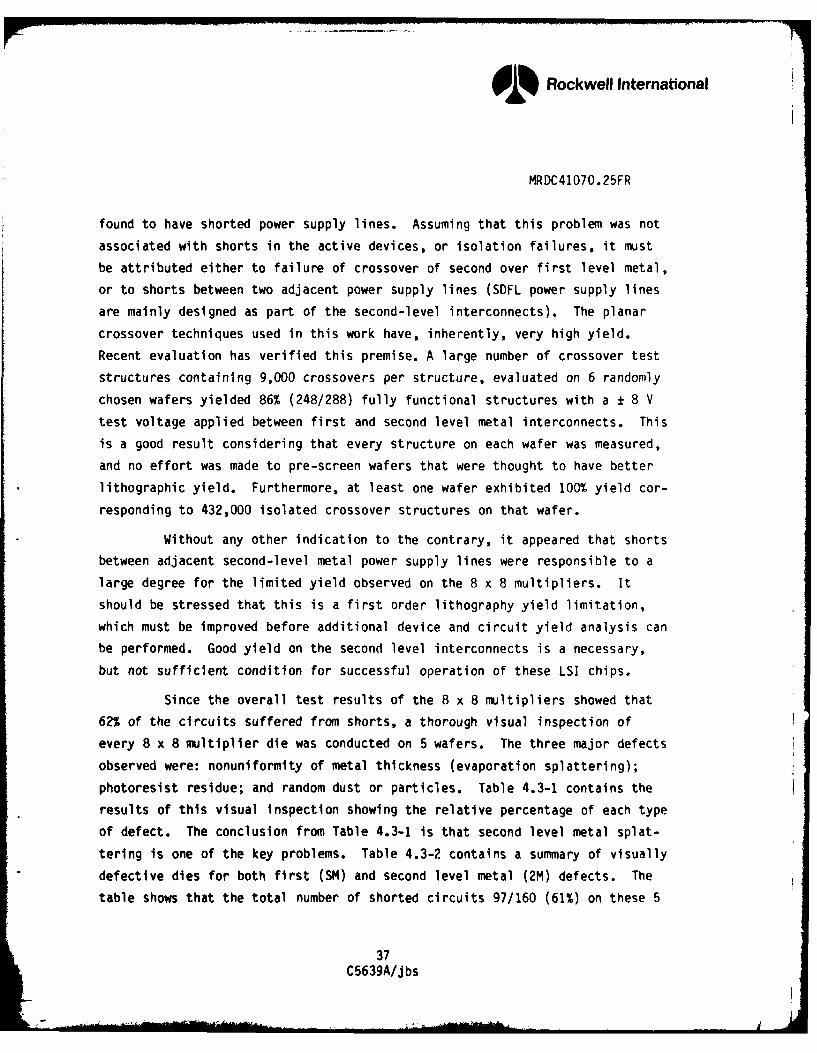
photoresist residue; and random dust or particles. Table 4.3-1 contains the
results of this visual inspection showing the relative percentage of each type
of defect. The conclusion from Table 4.3-1 is that second level metal splat-
tering is one of the key problems. Table 4.3-2 contains a summary of visually
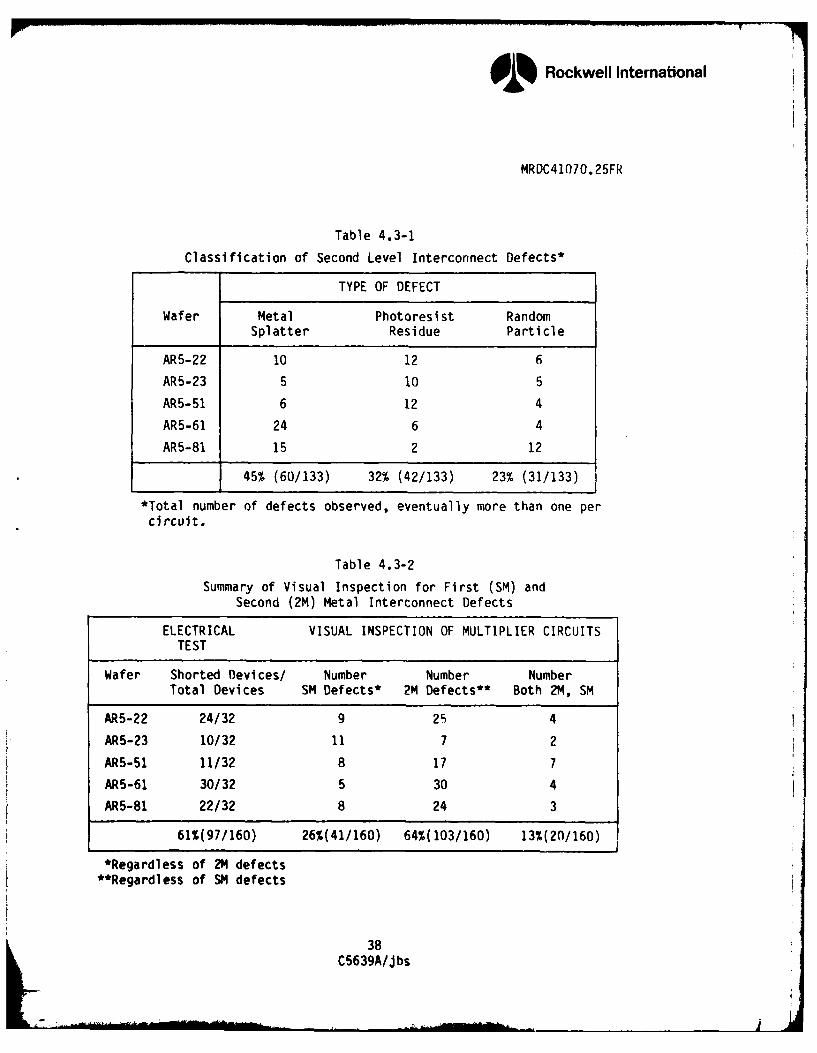
defective dies for both first (SM) and second level metal (2M) defects. The
table shows that the total number of shorted circuits 97/160 (61%) on these 5
37C5639A/j bs
Rockwell International
MRDC41O70.25FR
Table 4.3-1
Classification of Second Level Interconnect Defects*
TYPE OF DEFECT
Wafer Metal Photoresist RandomSplatter Residue Particle
AR5-22 10 12 6
AR5-23 5 10 5
AR5-51 6 12 4
AR5-61 24 6 4
AR5-81 15 2 12
45% (60/133) 32% (42/133) 23% (31/133)
*Total number of defects observed, eventually more than one per
circuit.
Table 4.3-2
Summary of Visual Inspection for First (SM) andSecond (2M) Metal Interconnect Defects
ELECTRICAL VISUAL INSPECTION OF MULTIPLIER CIRCUITSTEST
Wafer Shorted Devices/ Number Number NumberTotal Devices SM Defects* 2M Defects** Both 2M, SM
AR5-22 24/32 9 21 4
AR5-23 10/32 11 7 2
AR5-51 11/32 8 17 7
AR5-61 30/32 5 30 4
AR5-81 22/32 8 24 3
61%(97/160) 26%(41/160) 64%(103/160) 13%(20/160)
*Regardless of 2M defects
**Regardless of SM defects
38C5639A/J bs
Rockwell International
MRDC41070.25FR
wafers is representative and in good agreement with the 62% electrical fail-
ures observed for all of the processed 8 x 8 multiplier wafers. As indicated
in Table 4.3-2 the largest number of defects (64%) was found on the second
level metal, with only 26% of the die showing first level metal defects. A
small percentage of the dies, 13%, had simultaneous first and second level
metal defects. In summary, the data collected from wafers with 8 x 8 multi-
pliers date indicate that the first order defects on the 8 x 8 multiplier cir-
cuits are in the second level interconnects. Efforts to improve the second
level metalization and interconnect are discussed in the rest of this section.
Second Level Metallizations
The second level interconnects are defined by ion milling, where
energetic ions bombard the surface and sputter atoms from it. Over etching is
the method used to insure complete removal of the desired material. However,
overetching is not adequate for completely removing all the material from
areas where the metal thickness is much greater than the average (splatter-
ing), or from areas which have foreign materials such as photoresist residues
or dust particles. Incompletely etched metal can result in defective shorted
patterns, and it can lead to problems such as shorted power supply lines.
The second level metalization was deposited by e-beam evaporation.
An appealing alternative deposition technique, magnetron sputtering, was in-
vestigated. Magnetron sputtered films have excellent via step coverage and do
not exhibit any splattering. The magnetron sputtering system used for these
experiments was equipped with a planetary fixture allowing films to be deposi-
ted with 03% thickness uniformity. However, this system, with a small (- 4")
target and a large planetary, deposits films of rather high resistivity. Be-
cause of the mechanism of the planetary, the substrate is traveling in and out
of the deposition zone, allowing Ar atoms to be trapped in the successive
layers of deposited material, thereby increasing the resistivity of deposited
films. The bulk resistivity of Au films deposited by magnetron sputtering is
0.040 0-jom, which is 1,7 times higher than films deposited by e-beam evapora-
39C5639A/jbs
01)% Rockwell International
MRDC41O7O.25FR
tion (0.0235 Q-Wm). This disadvantage of the magnetron sputtered films was
later reduced with the installation of a system compatible with 3 inch
diameter wafers.
To evaluate the improvements of second level metal process, a yield
test mask set was fabricated. The mask had two sets of inter-digitated lines
which can be electrically tested for shorts between two adjacent lines. A
sketch of the test structures is shown in Fig. 4.3-1. The mask set has both
light field and dark field versions so that it be can be used both with ion
milling and lift-off techniques. A photomicrograph of part of the test struc-
ture is shown in Fig. 4.3-2. Pattern A has 3 pm lines with 2 pM spacing, and
pattern B has 8 lin lines with 2 pM spacing. The length of each parallel line
is 1200 pM. Both patterns A and B have separated test sets which can be inde-
pendently analyzed. The total length of adjacent lines in a set starts with
12,000 pM and increases by doubling up to 144,000 pM. There are two pairs of
pattern A and B in each chip of 2.7 x 2.7 nmn; 72 pairs in a 25 x 25 nun wafer.
A direct comparison using the test mask described above indicates
that the yield of long parallel lines resulting from E-beam evaporation is
much lower than the yield resulting from magnetron sputtering as shown in Fig.
4.3-3. As the figure indicates, the yield for magnetron sputtering is 3 to 4
times higher than the best yield obtained by E-beam evaporation. The lower
yield obtained by E-beam evaporation is attribued to the splattering occurring
during evaporation.
In order to minimize splatter from evaporation, the evaporator used
for this experiment was upgraded so that the E-beam could be swept over the Au
source. However, the yields resulting from wafers deposited by this system(shown by triangles on Fig. 4.3-3) were still lower than those from magnetron
sputtering (squares on Fig. 4.3-3) while being more reproducible. The data
base was expanded by evaluating wafers on which Au was deposited by two evap-
orators used for other GaAs programs. It was found that the wafers processedwith the standard [C evaporation equipment had better yields. The points in
the Fig. 4.3-3 represent averages over the following data base:
40C5639A/J bs
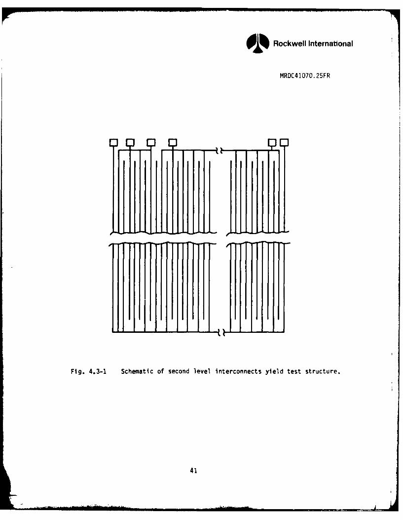
Rockwell International
MRDC4 1070. 25FR
Fig. 4.3-1 Schematic of second level interconnects yield test structure.
41
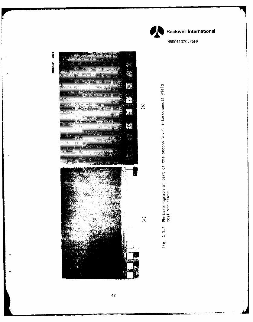
Rockwell International
MRDC4 1070. 25FR
-3
L
__4-_ 4-3
___._ 4-)
_ Ci
420
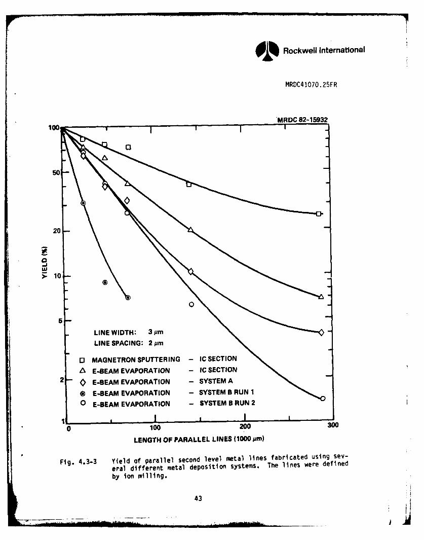
A) Rockwell International
MRDC41070.25FR
MRDC 82-15932
10--
00
so
10-
, 0 -
i 5-S LINE WIDTH: 3 m
LINE SPACING: 2 pm
o MAGNETRON SPUTTERING - IC SECTION
A E-BEAM EVAPORATION - IC SECTION
2 0 E-BEAM EVAPORATION - SYSTEM A
0 E-BEAM EVAPORATION - SYSTEM B RUN 1
o E-BEAM EVAPORATION - SYSTEM B RUN 2
0 100 200 300
LENGTH OF PARALLEL LINES (1000 Am)
Fig. 4.3-3 Yield of parallel second level metal lines fabricated using sev-
eral different metal deposition systems. The lines were defined
by ion milling.
43
Rockwell International
MRDC4107O.25FR
Magnetron Sputtering - IC Equipment 2 runs, 4 wafers/runE-Beam Evaporation - IC Equipment 2 runs, 4 wafers/runE-Beam Evaporation - System A 1 run, 4 wafers/runE-Beam Evaporation - System B, Run 1 1 run, 2 wafersE-Beam Evaporation - System B, Run 2 1 run, 2 wafers
In conclusion, magnetron sputtering resulted the best metal deposi-
tion technique for second level interconnects, and it was adopted as the
standard technique in our fabrication line. Although some improvements in
specific resistivity are desirable, the current resistivity values are quite
acceptable, and they are taken into account in the design.
Multi -Level Interconnects
As the complexity and size of the integrated circuits increase, the
number of multi-level interconnects and crossovers increases dramatically.
Therefore, the integrity and yield of crossover structures and multi-level
interconnects is an important factor for successful LSI/VLSI fabrication. The
yields of crossover structures were discussed earlier in this section. Here,
the results from the evaluation of the yield of long chains of interconnects,
are presented.
The interconnect test structure used in this study consists of achain of first to second level metal interconnects. A drawing of the cellused to build the long chain is shown in Fig. 4.3-4. Alternating short stripsof Schottky (first level) metal and second level metal are interconnectedthrough via holes. To save space on the wafers, the interconnect test struc-
ture was laid out as a long meander in the kerf lines. A portion of the
pattern is shown in Fig. 4.3-5. The total length of the pattern includes
14878 interconnects. Note, as a reference, that an 8 x 8 multiplier (1000
gates circuit) has -7000 interconnects. The interconnect pattern has taps at
intermediate points so that yield can be measured for several lengths of the
chain.
44C5639A/J bs
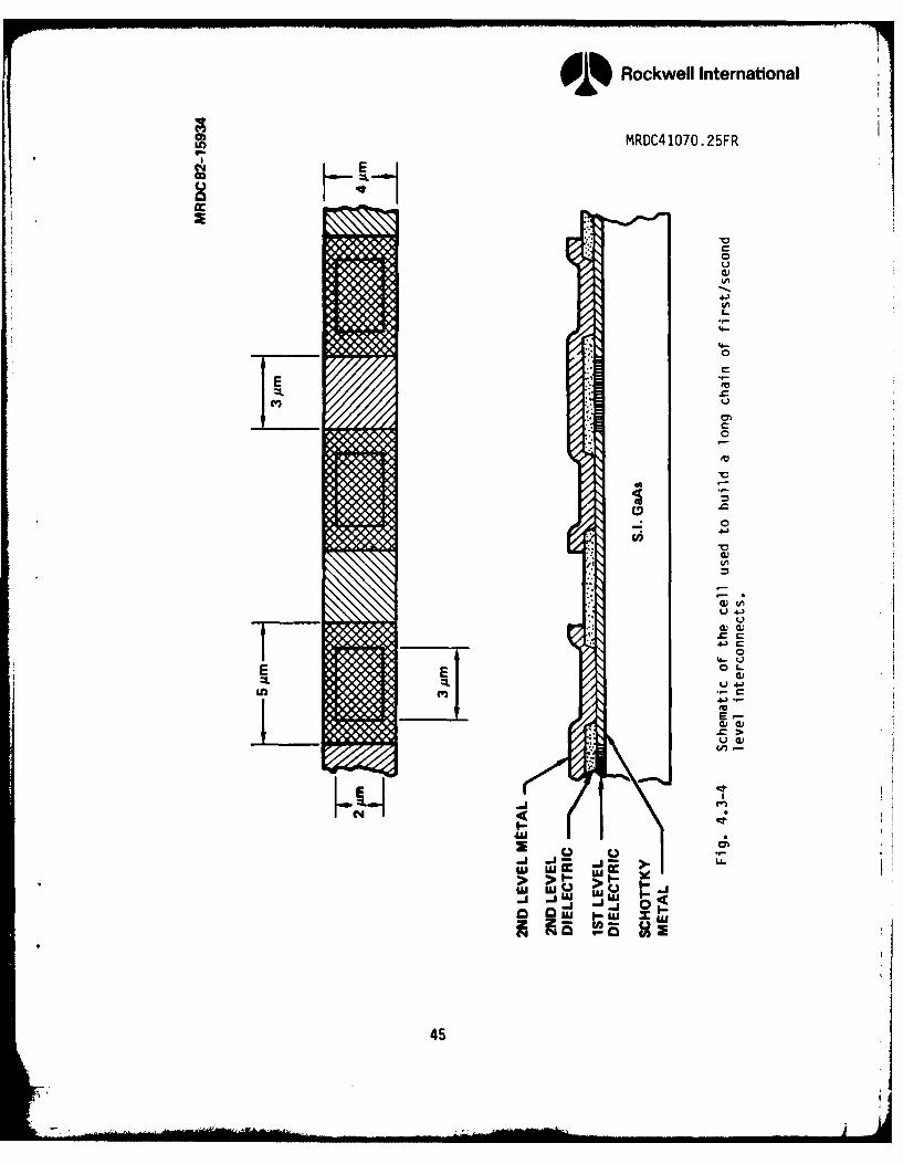
Rockwell International
*MRDC41070.25FR
aEUL
I-
C.V)
C C' 0U
E E
.t-
0
Lb m C
E
AUU
C0
3EU
- 0- o
U 4XW
45
--
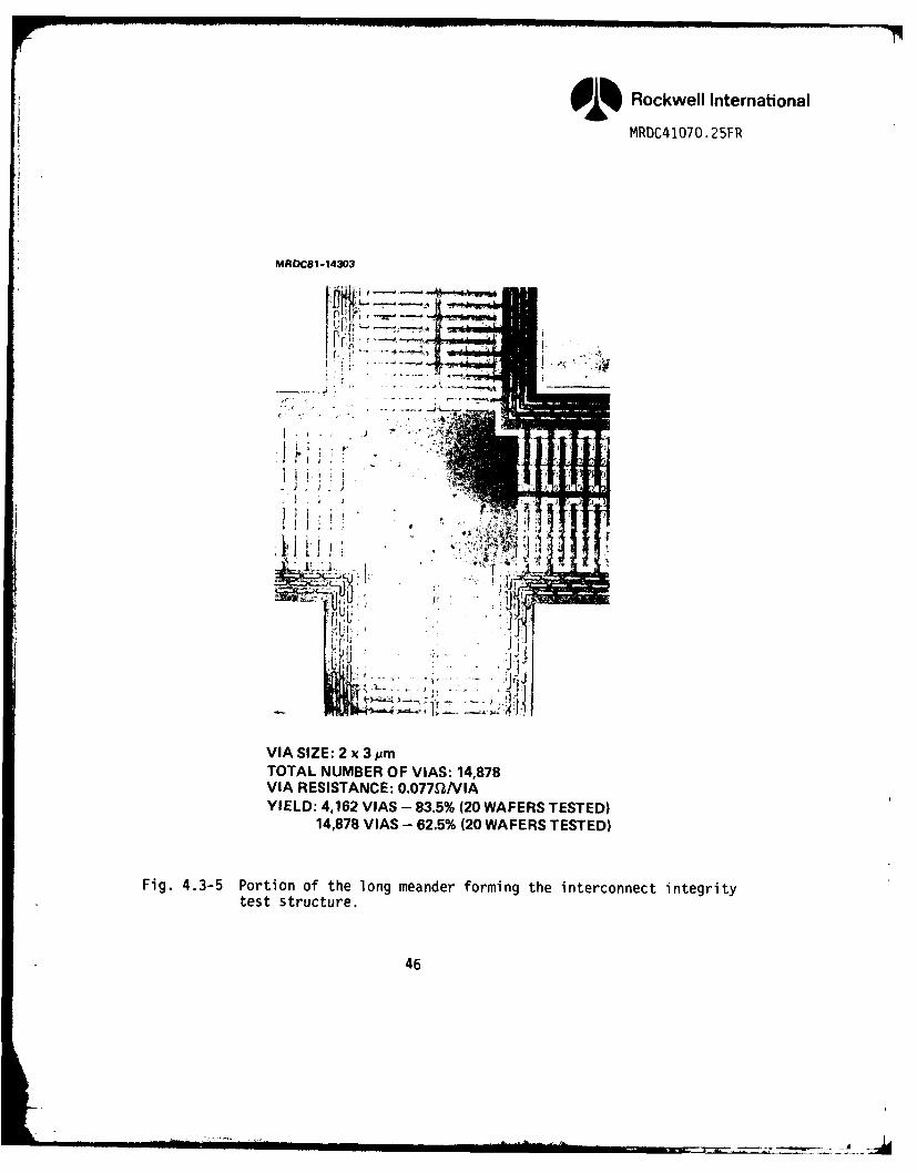
A~Rockwell International
MRDC41070-25FR
MRA3CSI-14303
; JI ak'
VIA SIZE: 2 x 3pmTOTAL NUMBER OF VIAS: 14,878VIA RESISTANCE: 0.07712NIAYIELD: 4,162 VIAS - 83.5% (20 WAFERS TESTED)
14,878 VIAS - 62.5% (20 WAFERS TESTED)
Fig. 4.3-5 Portion of the long meander forming the interconnect integritytest structure.
46
0 % Rockwell International
MRDC41O7O.25FR
The integrity of the interconnects was electrically tested by inject-
ing a current of 4 mA through the string. The test can only determine if a
string of interconnects is continuous (has current flow) or broken (has no
current flow). The test cannot indicate if any elements in the string are
shorted together unless a long chain of the string is shorted so that an
abnormally low resistance is observed.
The yields obtained are indicated in Fig. 4.3-6. They represent the
averages obtained from 20 wafers. The yield of 400 interconnects is 100%. Itdecreases slowly to -65% for the maximum number (14878) of interconnects.
The interpolated yield for 7000 interconnects, the number in the 8 x 8 SDFL
multiplier, is slightly over 80%. This is a satisfactory number today. How-
ever, further improvements will be needed for higher circuit complexity.
The average resistance of each via is 0.077 9, which is approximately
equal to the resistivity of a square of 3000A thick Au Schottky metal
(0.078 Q/01). This value is low enough because it means that the interconnectresistance is negligible with respect to the line resistance. From a process
standpoint, this low value indicates that the surface of the Schottky (first
level) metal inside the vias are clean after via window etching, and the
second level and first level metal make very good contact.
4.4 Fabrication of 1-inch Wafers
Seven lots (of 4 wafers each) were processed using mask set AR6 (see
Sec. 5 for a description of the circuits on this mask set). All the wafers
were characterized by our standard parametric test procedure based on the
automatic test of arrays of test structures placed on all wafers.
A sample of such parametric data is shown in Figs. 4.4-1 and 4.4-2.
The data in Fig. 4.4-1 represent a histogram of threshold voltages for the 48
test FETs (50 Mj channel width, 1 Mj gate length) distributed across the 1
inch square wafer. A wafer map is shown on the left. The average threshold
voltage, VP a -1.02 V is within the desired range of 0.9-1.3 V, and the wafer
standard deviation of 72 miV is quite typical (best values are -30 mV). A
47C5639A/J bs
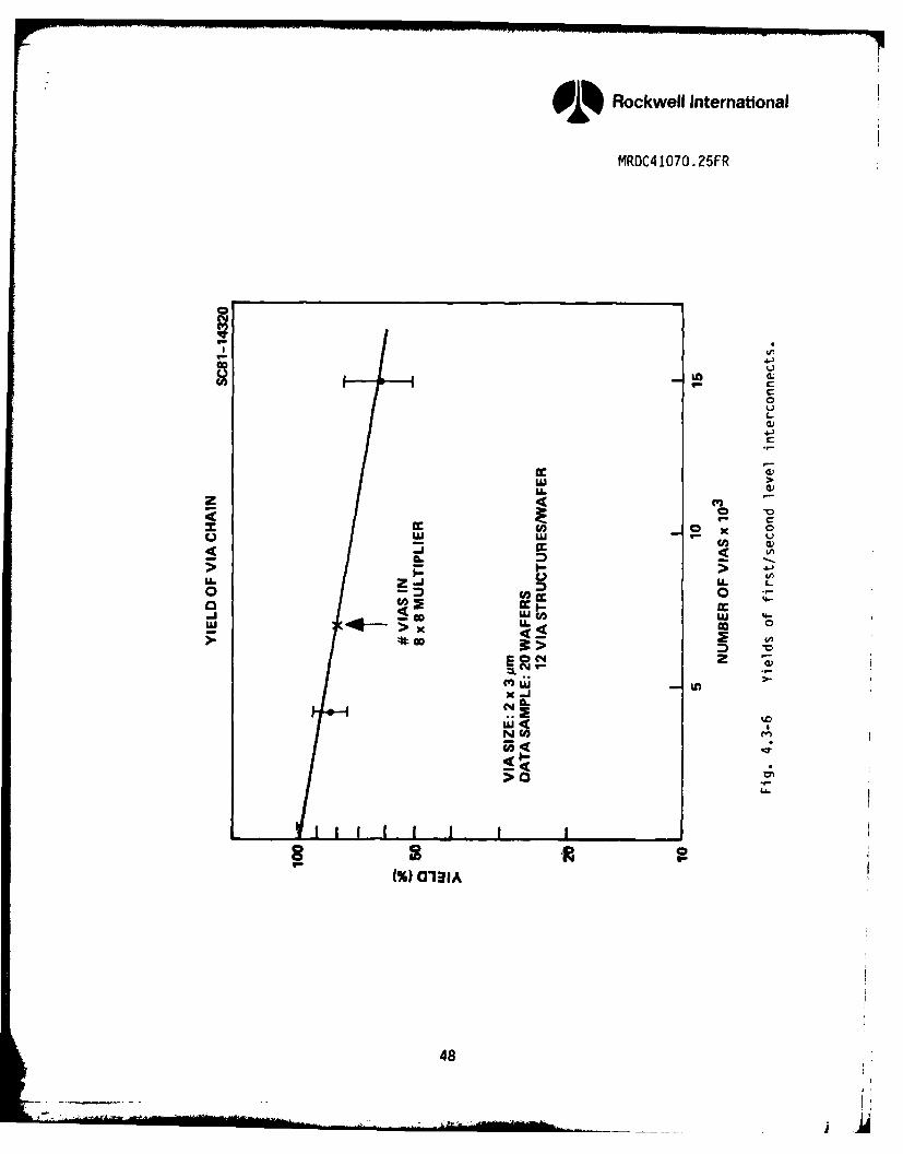
Rockwell International
I-I
MRDC4 I070.25FR
C
W W
0
..
M. Z.I - 4. 4.,
CAC
LU 0
'> >
0 - 0 0LU LU x
>U. >L
G>
x2 _CVL
LU(N '
M 0131A
48
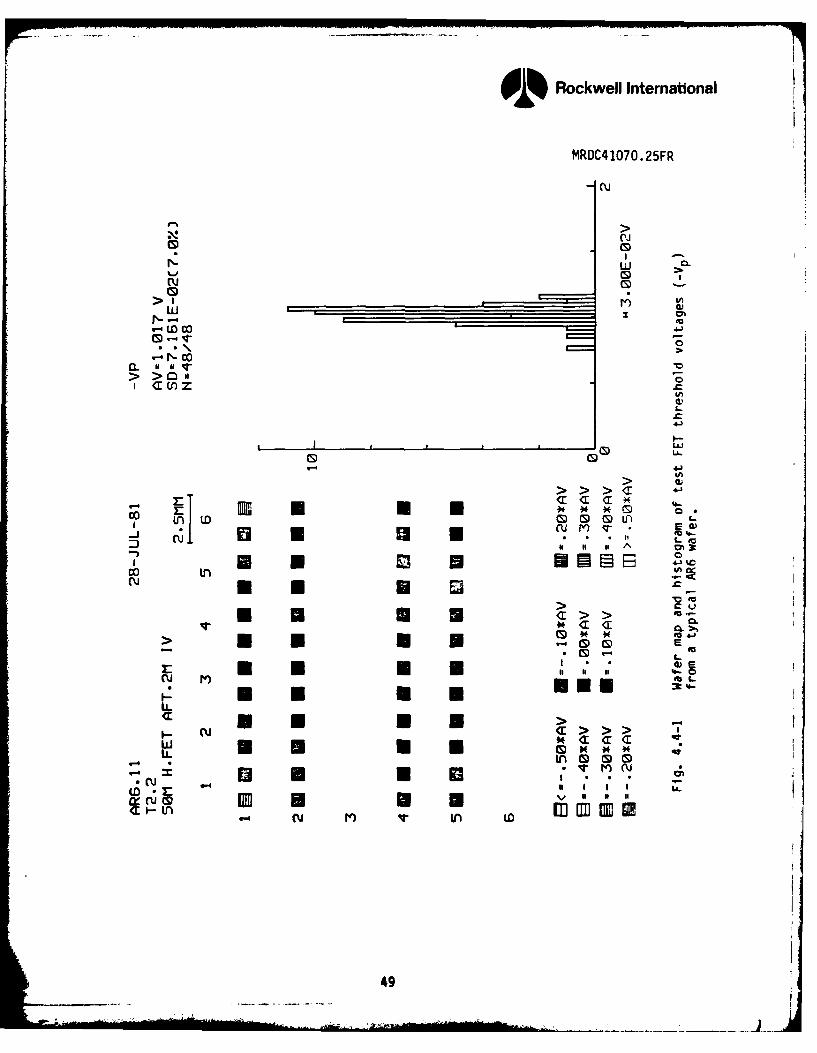
Rockwell International
MRDC41070.25FR
CJ
LIU
(U> IV
p- 00
a- vii~->->0O -
LJ
CS G U U
4-3
N Q** *
co n .S S S)U) EQ
CuC
>
'- * m 41
N >
49 q- VN
49
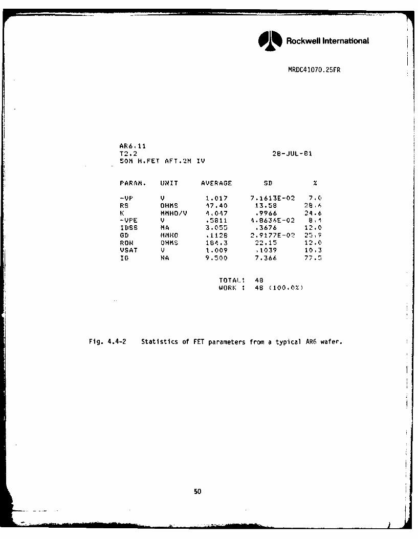
OD Rockwell International
MRDC41070.25FR
AR6, 11T2,2 28-JUL-8150M H,FET AFT.2M IV
PARAM, UNIT AVERAGE SDx
-VP V 1.017 7.1613E-02 7.0RS OHMS 17.40 13.58 2816K MMHO/V 4,047 .9966 24.6-VPE V .5811 4.8636E-02 BaIDSS MA 3.055 .3676 12.0G1 MMHO t1128 2.9177E-02 25,9RON OHMS 184,3 22.15 12.0VSAT V 1.009 ,t039 10,3IC NA 9.500 7.366 77.5
TOTAL1 48WORK : 48 (100.0%)
Fig. 4.4-2 Statistics of FET parameters from a typical AR6 wafer.
50
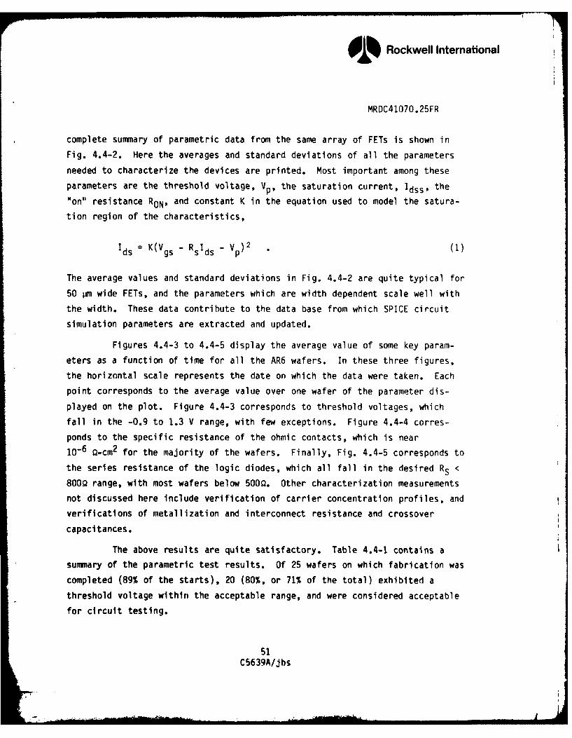
'~Rockwell International
MRDC41O7O.25FR
complete summnary of parametric data from the same array of FETs is shown in
Fig. 4.4-2. Here the averages and standard deviations of all the parameters
needed to characterize the devices are printed. Most important among these
parameters are the threshold voltage, VP, the saturation current, ldss, thelio" resi stance RON, and constant K in the equation used to model the satura-
tion region of the characteristics,
Ids K(VsRd -V )2 *(1)
The average values and standard deviations in Fig. 4.4-2 are quite typical for
50 Mi wide FETs, and the parameters which are width dependent scale well with
the width. These data contribute to the data base from which SPICE circuit
simulation parameters are extracted and updated.
Figures 4.4-3 to 4.4-5 display the average value of some key param-
eters as a function of time for all the AR6 wafers. In these three figures,
the horizontal scale represents the date on which the data were taken. Each
point corresponds to the average value over one wafer of the parameter dis-
played on the plot. Figure 4.4-3 corresponds to threshold voltages, which
fall in the -0.9 to 1.3 V range, with few exceptions. Figure 4.4-4 corres-
ponds to the specific resistance of the ohmic contacts, which is near10-6 g-cm2 for the majority of the wafers. Finally, Fig. 4.4-5 corresponds to
the series resistance of the logic diodes, which all fall in the desired RS <
800Q range, with most wafers below 5009. Other characterization measurements
not discussed here include verification of carrier concentration profiles, and
verifications of metallization and interconnect resistance and crossover
capacitances.
The above results are quite satisfactory. Table 4.4-1 contains a
summary of the parametric test results. Of 25 wafers on which fabrication was
completed (89% of the starts), 20 (80%, or 71% of the total) exhibited a
threshold voltage within the acceptable range, and were considered acceptable
for circuit testing.
51C5639A/Jbs
Rockwell International
MRDC41070.25FR
4.S I I i i I 5 1 1 1 I I I I I I I I I i I I I i r
C %CIw
'-A-w 5,2
o ~- LU)
CM
O ..-C
000
UO'L
30
060
m- o
0v
oO *00
OLLLL
C V-4 00.
52
L
I o . . . :. ,, ,. , ; i- ' W
. . . .. . . ... ,.. .. 0
U) InI
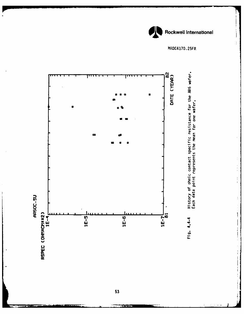
01%Rockwell International
MRDC4170.25FR
aa
* - CC
EOr,4.
W EU
C- C0. o
1A
4j~
0~ CL
u
CL4-)
L;C
0 0j
la g -l l
C~~ (mtP(W, 0 0, W
0 L.
OUW
4.)LJ C
u0
53,
IDI
LiL
z -€
0 IL0
'-I-
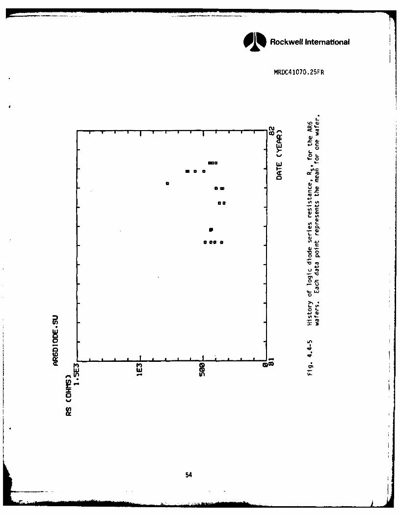
9 Rockwell International
MRDC41070.25FR
L:* I I * I I * I I *
rraOD
4-. 0w .0 .
a a o a:
SE U G)
C
4A
4j
d)0.
La:mam .,- 4)
C;
4
iU
CL
- IA U-I i
54
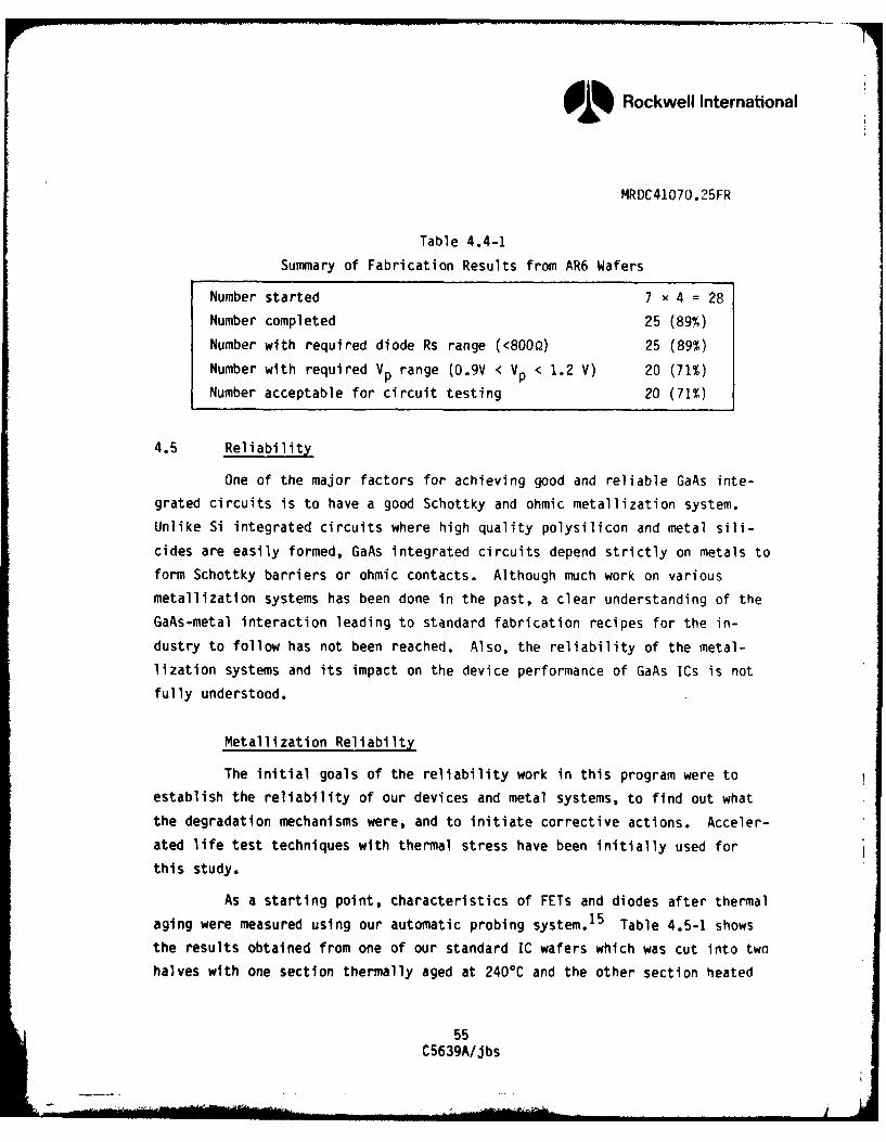
91) Rockwell International
MRDC41070.25FR
Table 4.4-1
Summary of Fabrication Results from AR6 Wafers
Number started 7 x 4 = 28
Number completed 25 (89%)
Number with required diode Rs range (<800Q) 25 (89%)
Number with required Vp range (O.9V < V p < 1.2 V) 20 (71%)
Number acceptable for circuit testing 20 (71%)
4.5 Reliability
One of the major factors for achieving good and reliable GaAs inte-
grated circuits is to have a good Schottky and ohmic metallization system.
Unlike Si integrated circuits where high quality polysilicon and metal sili-
cides are easily formed, GaAs integrated circuits depend strictly on metals to
form Schottky barriers or ohmic contacts. Although much work on various
metallization systems has been done in the past, a clear understanding of the
GaAs-metal interaction leading to standard fabrication recipes for the in-
dustry to follow has not been reached. Also, the reliability of the metal-
lization systems and its impact on the device performance of GaAs ICs is not
fully understood.
Metallization Reliabilty
The initial goals of the reliability work in this program were to
establish the reliability of our devices and metal systems, to find out what
the degradation mechanisms were, and to initiate corrective actions. Acceler-
ated life test techniques with thermal stress have been initially used for
this study.
As a starting point, characteristics of FETs and diodes after thermal
aging were measured using our automatic probing system. 15 Table 4.5-1 shows
the results obtained from one of our standard IC wafers which was cut into two
halves with one section thermally aged at 2400C and the other section heated
55C5639A/Jbs
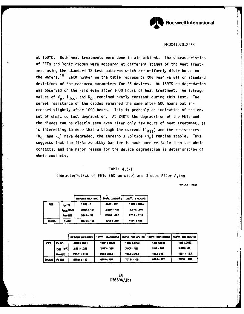
Rockwell International
MRDC41070.25FR
at 1500C. Both heat treatments were done in air ambient. The characteristics
of FETs and logic diodes were measured at different stages of the heat treat-
ment using the standard T2 test patterns which are uniformly distributed on
the wafers.1 5 Each number on the table represents the mean values or standard
deviations of the measured parameters for 36 devices. At 1500C no degradation
was observed on the FETs even after 1000 hours of heat treatment. The average
values of Vp, Idss , and Ron remained nearly constant during this test. The
series resistance of the diodes remained the same after 500 hours but in-
creased slightly after 1000 hours. This is probably an indication of the on-
set of ohmic contact degradation. At 2400C the degradation of the FETs and
the diodes can be clearly seen even after only few hours of heat treatment. It
is interesting to note that although the current (Idss) and the resistances
(Ron and Rs) have degraded, the threshold voltage (Vp) remains stable. This
suggests that the Ti/Au Schottky barrier is much more reliable than the ohmic
contacts, and the major reason for the device degradation is deterioration of
ohmic contacts.
Table 4.5-1
Characteristics of FETs (50 pm wide) and Diodes After Aging
MROC81-11564
BEFORE HEATING 240°C 2 HOURS 240C 4 HOURS
FIE VP IV) 1I 6.1 4027t.102 11.0104
(a) 204 t 36 2966. t46 276.7 t 61.0
S Rs () 7 2± 106 1243 ± 14 3 401
SEPOREHEATING 160C 124HOURS 160C 336HOURS 0C 62 IHOURS 15C 6MHOU
-FET VpVI Am A01 1llt7 1.607640 /INA 1.02 t614 1A06±"
IM Il 2 2 1233 233 t 2.1W61210 2.0±9 I2 I. -.3
Ron 27 t 321.9 =2Ait22 17.22 t620.2 1.1 * W1
om e mlta 6736±11 60.8±t106 701.6±106e e7ebt *7 ma!0±in
56C5639A/jbs
Q% Rockwell International
MRDC41070.25FR
Ohmic contact reliability studies were conducted on test structures
similar to the cross section of the metallization system for our standard FETs
shown in Fig. 4.5-1. The ohmic contacts in the source and drain area consist
of two layers of metals. The first layer is the alloyed ohmic metal, AuGe/Pt
at the time when those experiments were conducted; the second layer is Ti/Au,
which is the same metal used for the Schottky barrier gates.
In order to obtain direct measurement of the ohmic contact resistance
an improved TLM test structure 14 which utilizes several ohmic gaps with dif-
ferent gap lengths was included in the AR5 mask set (designed and fabricated
on a previous program). 1 This specific contact resistance structure was re-
peated so that a statistical sample size of 72 can be obtained from each
wafer. The contact resistance of several wafers was monitored at frequent
intervals during thermal aging tests, and these results were correlated with
the device and circuit performance data.
The conclusion reached was that AuGe/Pt by itself forms excellent
ohmic contact with GaAs, exhibited by low contact resistance and good morphol-
ogy. Table 4.5-2 shows the specific contact resistance of AuGe/Pt contacts at
different stages of aging at 2500C up to 300 hours. Little or no degradation
was observed.
Table 4.5-2
Specific Contact Resistance (Q-cm 2) of AuGe/Pt Ohmic Contacts
Without Schottky Overlay Heat Treated at 2500C
As Alloyed 2 Hours 10 Hours 50 Hours 150 Hours 300 Hours
4 x 10⁻⁶ 7.3 x 10⁻⁶ 7.7 x 10⁻⁶ 5.6 x 10- 6 4.6 x 10⁻⁶ 4.9 x 10"6
The effect of varying the doping concentration (over a limited range)
on the contact resistance was also studied. The dose of n+ sulfur implant was
varied over a range of sheet resistance from 250 9/0 up to 750 Q/0 . (Our
typical sheet resistance is - 500 0/0 ). Table 4.5-3 shows the specific con-
tact resistance and their reliability data corresponding to 4 different
57C5639A/jbs
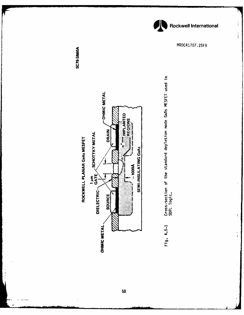
Rockwell International
MRDC4 1707. 25FR
.. ZCz
LU *J
LU >
o CC,
00
E E
3: LU C 0
LU 0
4' 0
58--
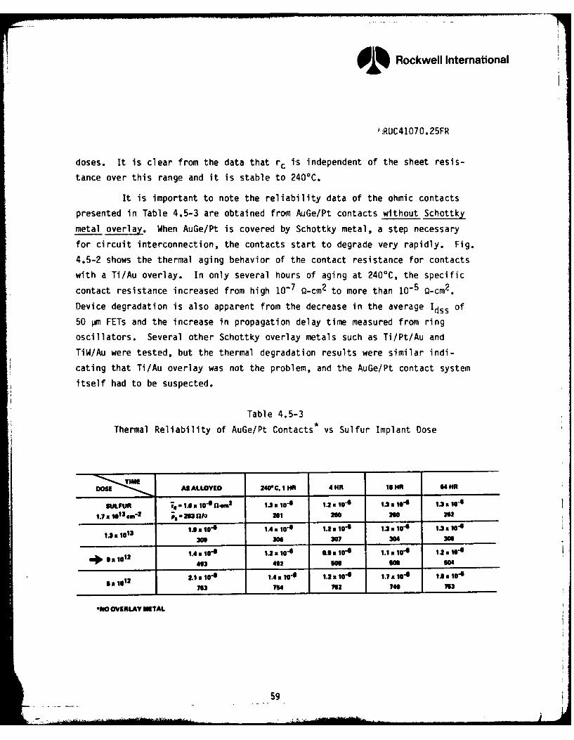
Rockwell InternationalI.
i;RDC41070.25FR
doses. It is clear from the data that rc is independent of the sheet resis-
tance over this range and it is stable to 2400C.
It is important to note the reliability data of the ohmic contacts
presented in Table 4.5-3 are obtained from AuGe/Pt contacts without Schottky
metal overlay. When AuGe/Pt is covered by Schottky metal, a step necessary
for circuit interconnection, the contacts start to degrade very rapidly. Fig.
4.5-2 shows the thermal aging behavior of the contact resistance for contacts
with a Ti/Au overlay. In only several hours of aging at 240 0C, the specific
contact resistance increased from high 10- 7 g-cm 2 to more than 10- 5 Q-cm 2.
Device degradation is also apparent from the decrease in the average Idss of
50 pm FETs and the increase in propagation delay time measured from ring
oscillators. Several other Schottky overlay metals such as Ti/Pt/Au and
TiW/Au were tested, but the thermal degradation results were similar indi-
cating that Ti/Au overlay was not the problem, and the AuGe/Pt contact system
itself had to be suspected.
Table 4.5-3
Thermal Reliability of AuGe/Pt Contacts* vs Sulfur Implant Dose
AS ALLOYED 2408C. 1 MR 4HR IsHR 64MHR
SULFUR * 1,. x 10-0 n.m 2 1.3 x 10 4 1.2 1I, 104 1.3. 10.16
1.7 10 13 m"2 " 263 n/a NI 200 260 262
In 3 is x 10- 0 1.4 n
10-4 1.2 x 10⁴ 1..104 1.3 a 10-
4
30 3 307 304 30
= 11 1.4 x 10⁴ 11 x 10-
4 0.0 • 10 4 1.1 104 1.28=10
.0
493 492 B0" 50 604
- .1 • 10 1.4 • 10.'4 1.2 a 10 .6 1.7 a 10. 4 1.1 a to-$
3 714 762 1 740 1 63
"NO OVERLAY ETAL
59
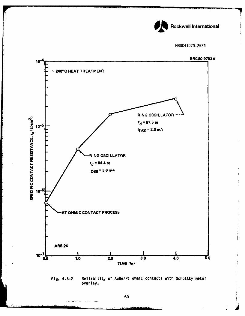
Rockwell International
MRDC41O7O. 25FR
10-4 ERCO-9703A
2400 C HEAT TREATMENT
RING OSCILLATOR-.\
10b-5 -7=975p- DS- . n
dJ02
RING OSCILLATOR
IDSS3.m
2U.
AT OHMIC CONTACT PROCESS
AR5-24
0.0 1.0 2.0 3.0 4.0 5.0TIME (hr)
Fig. 4.5-2 Reliability of AuGe/Pt ohmic contacts with Schottky metaloverlay.
60
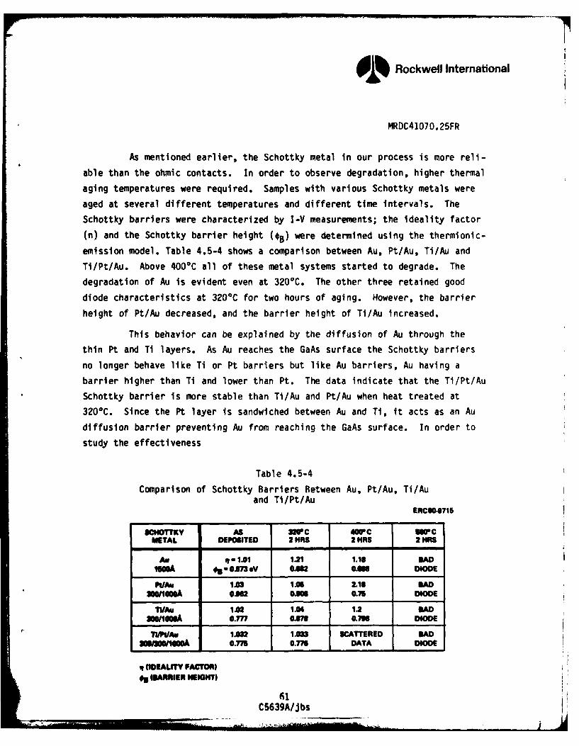
Rockwell International
MRDC41070.25FR
As mentioned earlier, the Schottky metal in our process is more reli-
able than the ohmic contacts. In order to observe degradation, higher thermal
aging temperatures were required. Samples with various Schottky metals were
aged at several different temperatures and different time intervals. The
Schottky barriers were characterized by I-V measurements; the ideality factor
(n) and the Schottky barrier height (OB) were determined using the thermionic-
emission model. Table 4.5-4 shows a comparison between Au, Pt/Au, Ti/Au and
TI/Pt/Au. Above 4000C all of these metal systems started to degrade. The
degradation of Au is evident even at 3200C. The other three retained good
diode characteristics at 3200C for two hours of aging. However, the barrier
height of Pt/Au decreased, and the barrier height of Ti/Au increased.
This behavior can be explained by the diffusion of Au through the
thin Pt and Ti layers. As Au reaches the GaAs surface the Schottky barriers
no longer behave like Ti or Pt barriers but like Au barriers, Au having a
barrier higher than Ti and lower than Pt. The data indicate that the Ti/Pt/Au
Schottky barrier is more stable than Ti/Au and Pt/Au when heat treated at
3200C. Since the Pt layer is sandwiched between Au and Ti, it acts as an Au
diffusion barrier preventing Au from reaching the GaAs surface. In order to
study the effectiveness
Table 4.5-4
Comparison of Schottky Barriers Between Au, Pt/Au, Ti/Auand TI/Pt/Au
ERC10-715
SCHOTTKY AS 3209C 4SC 0CMETAL DEPOSITED 2 MRS 2 HRS 2 HRS
AN q,1.01 1.21 1.13 mAD"00A 0.071V 0.42 0136 DIODE
It/Au 1.03 1. 2.10 BAD11olooA 02 0..96 UM7S DIODE
Ti/Au 1.02 104 1.2 BADolooM o.777 0.r76 9796 DIODE
WTA/PV 1.02 1.03 SCATTERED BAD8000MA 0.775 0.776 DATA DIODE
(IDEALITY FAcTOR)/WARRIER sW)
C5639A/J bs
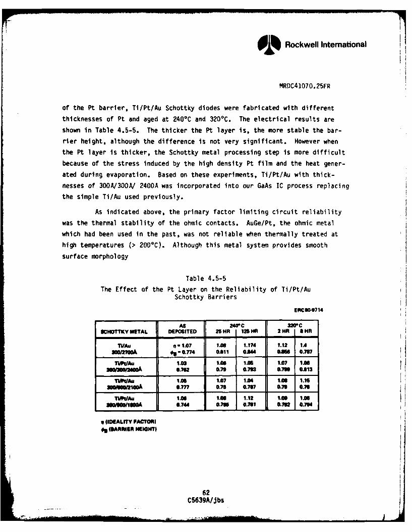
Rockwell International
NRDC41070.25FR
of the Pt barrier, TI/Pt/Au Schottky diodes were fabricated with different
thicknesses of Pt and aged at 2400C and 320°C. The electrical results are
shown in Table 4.5-5. The thicker the Pt layer is, the more stable the bar-
rier height, although the difference is not very significant. However when
the Pt layer is thicker, the Schottky metal processing step is more difficult
because of the stress induced by the high density Pt film and the heat gener-
ated during evaporation. Based on these experiments, Ti/Pt/Au with thick-
nesses of 300A/30OA/ 2400A was incorporated into our GaAs IC process replacing
the simple Ti/Au used previously.
As indicated above, the primary factor limiting circuit reliability
was the thermal stability of the ohmic contacts. AuGe/Pt, the ohmic metal
which had been used in the past, was not reliable when thermally treated at
high temperatures (> 2000C). Although this metal system provides smooth
surface morphology
Table 4.5-5
The Effect of the Pt Layer on the Reliability of Ti/Pt/Au
Schottky Barriers
ERC8O-9714
AS 240"C 32'CSCHOTTKY METAL DEPOSITED 25 HR 125 HR 2 HR 1 HR
TAu 1.07 I0 1.174 1.12 IA30/2"OmOA - 0.774 0.011 044 0356 0.737
TL/Au 1.03 10 1I05 1.07 1U030W30W2400A 0.2 0.79 0.73 0.7119 0.213
TijWAu 1.05 1.07 1.04 1.06 1.160baw0i02100A 0.m 0.78 0.737 0.73 0.78
Ti/ft/Av 1.06 1.06 1.12 1.03 1.0ISSoS~llOOA 0.744 0.705 0.781 0.732 0.794
it (IDEALITY FACTOR)0 (BARRIER HEIGHT)
62C5639A/J bs
Rockwell International
MRDC41070.25FR
and low contact resistance after alloying, it degrades rapidly when thermally
aged.
To improve the reliability of the ohmic contacts, another metal sys-
tem, AuGe/Ni, was studied, and its thermal reliability was evaluated. It was
found that this metal system was much more stable than AuGe/Pt. In order to
have a good comparison between these two systems, wafers were processed with
AuGe/Pt on one half and AuGe/Ni on the other half of the same wafer. All the
processing steps including the alloying cycle were the same for both metals.
The wafers were aged at 240 0C in air ambient for reliability testing. Speci-
fic contact resistance, device characteristics and circuit performance were
evaluated before and after aging.
In the following discussions the results from one of the wafers, AR5-
82 are used as an example. Half of the wafer has AuGe/Pt contacts. The spe-
cific contact resistance (rc) was determined by TLM (transmission line model)
method using the TI test pattern, which is uniformly distributed on the
wafer. 15 Table 4.5-6 shows the measured rc values at different stages of
processing and after thermal aging (at 2400 C). After the Schottky metalliza-
tion, the specific contact resistance of AuGe/Pt was already much higher than
that of AuGe/Ni. The AuGe/Ni contact continued to degrade with further proc-
essing and thermal aging. The degradation during the second level metal proc-
essing step is probably due to the heating cycle used during the deposition of
plasma silicon nitride. The rc for AuGe/Pt after Schottky metallization is
higher than the typical rc (in the 10-6 Q-cm 2 range) of AuGe/Pt immediately
after alloying. This indicates that the degradation had already occurred
during the Schottky metallization step. Degradation is probably due to the
thermal treatment involved in the processing and/or the influence of the
Schottky metal overlay. AuGe/Ni, on the other hand, had a very low initial rc
value (4 10-6 g-cm 2 ) and showed excellent thermal stability during process and
during thermal aging.
63
C5639A/jbs
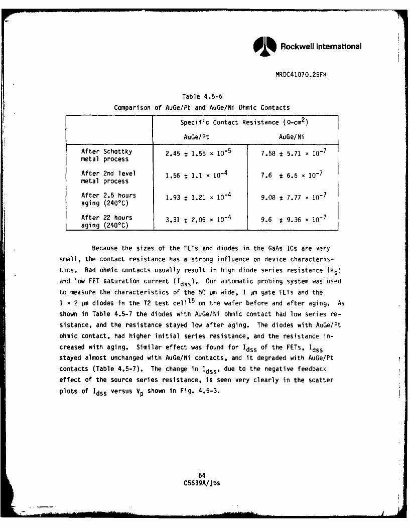
Rockwell International
MRDC41070.25FR
Table 4.5-6
Comparison of AuGe/Pt and AuGe/Ni Ohmic Contacts
Specific Contact Resistance (Q-cm 2 )
AuGe/Pt AuGe/Ni
After Schottky 2.45 ± 1.55 x 10⁻⁵ 7.58 ± 5.71 x 10⁻⁷
metal process
After 2nd level 1.56 ± 1.1 x 10⁻⁴ 7.6 t 6.6 x 10⁻⁷
metal process
After 2.5 hours 1.93 1 1.21 x 10⁻⁴ 9.08 t 7.77 x 10- 7
aging (240*C)
After 22 hours 3.31 ± 2.05 x 10- 4 9.6 ± 9.36 x 10⁻⁷
aging (2400C) I I
Because the sizes of the FETs and diodes in the GaAs ICs are very
small, the contact resistance has a strong influence on device characteris-
tics. Bad ohmic contacts usually result in high diode series resistance (Rs)
and low FET saturation current (Idss). Our automatic probing system was used
to measure the characteristics of the 50 pM wide, 1 pM gate FETs and the
1 x 2 pM diodes in the T2 test cell 15 on the wafer before and after aging. As
shown in Table 4.5-7 the diodes with AuGe/Ni ohmic contact had low series re-
sistance, and the resistance stayed low after aging. The diodes with AuGe/Pt
ohmic contact, had higher initial series resistance, and the resistance in-
creased with aging. Similar effect was found for Idss of the FETs, Idss
stayed almost unchanged with AuGe/Ni contacts, and it degraded with AuGe/Pt
contacts (Table 4.5-7). The change in Idss , due to the negative feedback
effect of the source series resistance, is seen very clearly in the scatter
plots of Idss versus Vp shown in Fig. 4.5-3.
64C5639A/J bs
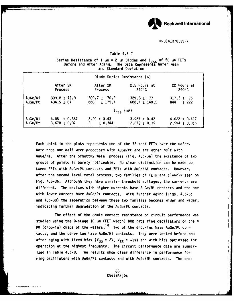
'iL Rockwell Intemational
MRDC41070.25FR
Table 4.5-7
Series Resistance of 1 pm x 2 pm Diodes and Idss of 50 uM FETsBefore and After Aging. The Data Represents Wafer Mean
and Standard Deviation
Diode Series Resistance (Q)
After SM After 2M 2.5 Hours at 22 Hours atProcess Process 2400C 2400C
AuGe/Ni 309.8 t 72.9 309.7 1 70.2 329.3 ± 77 317.3 ± 76AuGe/Pt 434.5 ± 87 668 ± 175.7 688.7 t 149.5 844 t 222
Idss (mA)
AuGe/Ni 4.05 ± 0.367 3.99 ± 0.43 3.967 1 0.42 4.022 t 0.417AuGe/Pt 3.678 t 0.37 3 t 0.344 2.872 ± 0.35 2.594 ± 0.316
Each point in the plots represents one of the 72 test FETs over the wafer.
Note that one half were processed with AuGe/Pt and the other half with
AuGe/Ni. After the Schottky metal process (Fig. 4.5-3a) the existence of two
groups of points is barely noticeable. No clear distinction can be made be-
tween FETs with AuGe/Pt contacts and FETs with AuGe/Ni contacts. However,
after the second level metal process, two families of FETs are clearly seen on
Fig. 4.5-3b. Although they have similar threshold voltages, the currents are
different. The devices with higher currents have AuGe/Ni contacts and the one
with lower current have AuGe/Pt contacts. With further aging (Figs. 4.5-3c
and 4.5-3d) the separation between these two families becomes wider and wider,
indicating further degradation of the AuGe/Pt contacts.
The effect of the ohmic contact resistance on circuit performance was
studied using the 9-stage 10 pin (FET width) NOR gate ring oscillators on the 4
PM (drop-in) chips of the wafers. 15 Two of the drop-ins have AuGe/Pt con-
tacts, and the other two have AuGe/Ni contacts. They were tested before and
after aging with fixed bias (VDD z 2V, VSS = -1V) and with bias optimized for
operation at the highest frequency. The circuit performance data are summar-
ized in Table 4.5-8. The results show clear difference in performance for
ring oscillators with AuGe/Pt contacts and with AuGe/Ni contacts. The ones
65C5639A/jbs
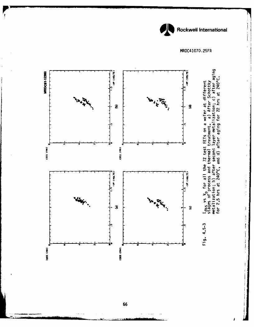
iqRockwell International
MRDC41O7O.25FR
T- C.U
L 4 4 J* 4- u~ M
%.- 0
a) 4-)to-to N
* UAO 4)
I'44 fa C ,
aiG= 4
66
01% Rockwell International
MRDC41070.25FR
with AuGe/Ni contacts oscillate faster and have lower speed-power product than
those with AuGe/Pt contacts. After aging for 22 hours at 240 0C, the ring
oscillators with AuGe/Pt contacts degraded; the propagation delay time in-
creased about 30 ps/gate. The ring oscillators with AuGe/Ni contacts main-
tained good speed after aging. No significant change in circuit performance
was observed. The best result obtained on this wafer showed a propagation
delay ID = 71 ps/gate and a speed-power product PdTD = 52 fJ. The circuit
performance data presented above agree with the specific contact resistance
data shown on Table 4.5-6 and the device data shown on Table 4.5-7.
Having recognized the difference in reliability between AuGe/Pt con-
tacts and AuGe/Ni contacts, the standard ohmic metallization system was
changed from AuGe/Pt to AuGe/Ni. This change resulted in significant improve-
ment in contact resistance. Figure 4.5-4 shows the history of the contact
resistance (Rc) and specific contact resistance (rc) over a relatively long
period of time. These data were obtained through the routine process evalua-
tion measurements taken with our automatic test facility. 15 Each point in the
graph represents the mean value of Rc or rc on a wafer. A transition at the
end of 1980 resulting in lower contact resistance as a consequence of replac-
ing AuGe/Pt by AuGe/Ni is clearly seen in the figure.
Circuit Reliability
The investigation of the reliability of GaAs integrated circuits is
more complex than that of discrete MESFETs. The complexity is due to the use
of more complex metallization systems, the need to maintain isolation between
devices, the large number of transistors and diodes on a chip, the complexity
of the dielectric systems, the length of interconnections, and the existence
of large numbers of crossovers. Preliminary work was done by high temperature
storage tests on 9-stage ring oscillators. The data showed an activation
energy of 1.41 eV for degradation, and a lifetime of more than 1013 hours at
room temperature was predicted. These figures are comparable to those that
have been reported for discrete GaAs MESFETs.
67C5639A/jbs
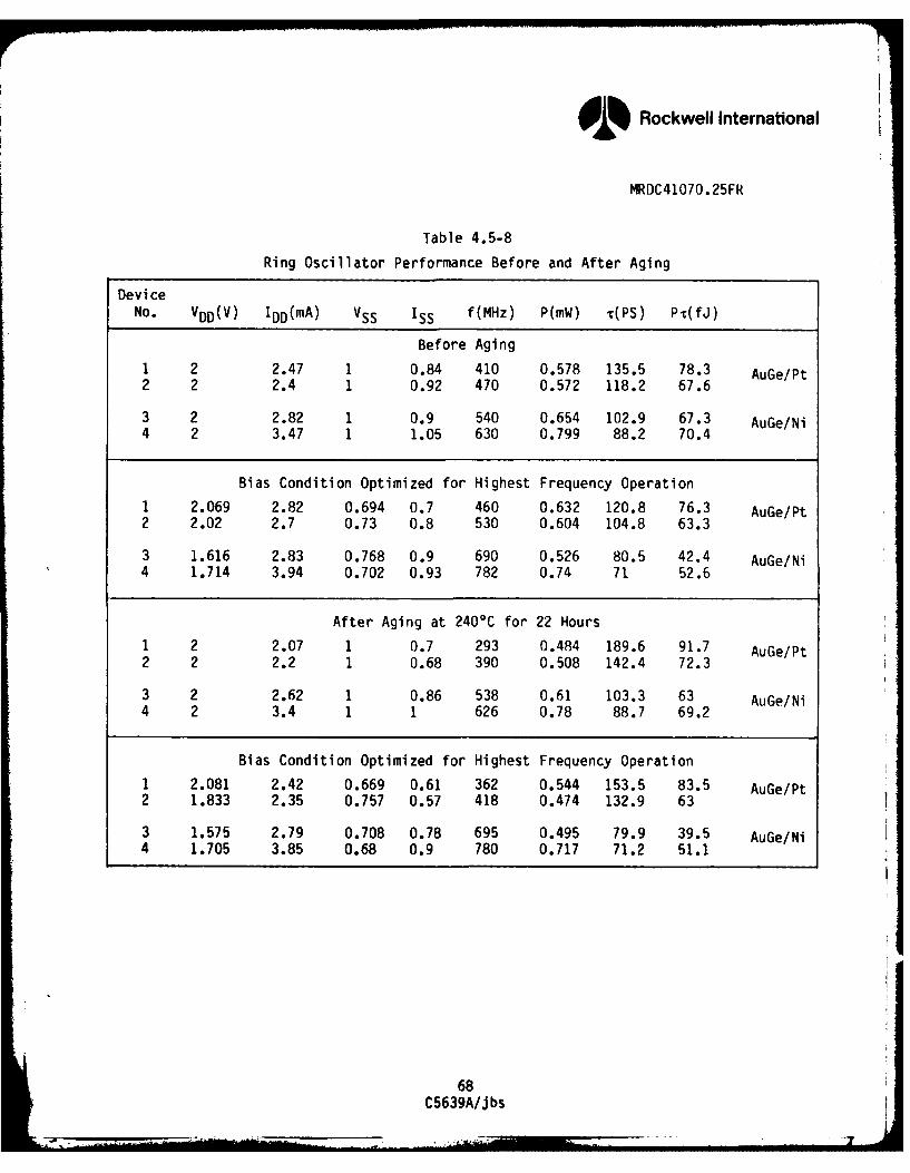
Rockwell International
MRDC41070.25FR
Table 4.5-8
Ring Oscillator Performance Before and After Aging
Device
No. VDD(V) IDD(mA) VSS ISS f(MHz) P(mW) r(PS) Pr(fJ)
Before Aging
1 2 2.47 1 0.84 410 0.578 135.5 78.3 AuGe/Pt2 2 2.4 1 0.92 470 0.572 118.2 67.6
3 2 2.82 1 0.9 540 0.654 102.9 67.3 AuGe/Ni4 2 3.47 1 1.05 630 0.799 88.2 70.4
Bias Condition Optimized for Highest Frequency Operation
1 2.069 2.82 0.694 0.7 460 0.632 120.8 76.3 AuGe/Pt2 2.02 2.7 0.73 0.8 530 0.604 104.8 63.3
3 1.616 2.83 0.768 0.9 690 0.526 80.5 42.4 AuGe/Ni4 1.714 3.94 0.702 0.93 782 0.74 71 52.6
After Aging at 240C for 22 Hours
1 2 2.07 1 0.7 293 0.484 189.6 91.7 AuGe/Pt2 2 2.2 1 0.68 390 0.508 142.4 72.3
3 2 2.62 1 0.86 538 0.61 103.3 63 AuGe/Ni4 2 3.4 1 1 626 0.78 88.7 69.2
Bias Condition Optimized for Highest Frequency Operation
1 2.081 2.42 0.669 0.61 362 0.544 153.5 83.5 AuGe/Pt2 1.833 2.35 0.757 0.57 418 0.474 132.9 63
3 1.575 2.79 0.708 0.78 695 0.495 79.9 39.5 AuGe/Ni4 1.705 3.85 0.68 0.9 780 0.717 71.2 51.1
68C5639A/jbs
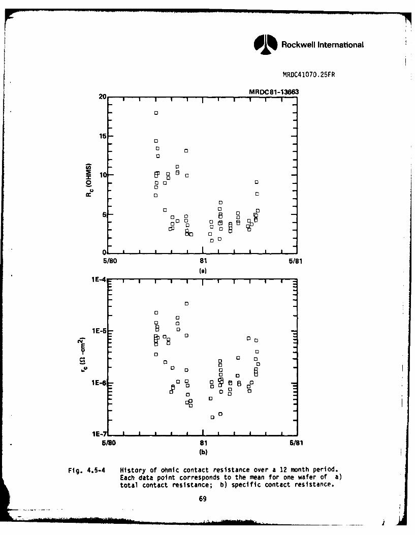
Rockwell International
MRDC41070.25FR
MRDC81-1366320 ,
15-0
0
0l- E O
S10- o0o
00 00
000 0
D 000 0
5-o0 B °o o_ oo o o B 0
0 ' II I I I i p i
5/80 81 5/81(a)
1E-4
0 00
0 0
1E-5 B o~08 0 00
N 00 o 00 0 0 0
0 0 00 0I1E-6- Po 0 0 @ () 8 o
o 0 -- 0 0
0 0
0 0
I E-7I a I5/80 81 5/81
(b)
Fig. 4.5-4 History of ohmic contact resistance over a 12 month period.Each data point corresponds to the mean for one wafer of a)total contact resistance; b) specific contact resistance.
69
___ l

Rockwell International
MRDC41070.25FR
Further reliability studies have been carried out on circuits under
bias. Ring oscillators with 9 inverter stages were chosen for this study.
Each stage in the circuits contained a 10pM wide switching FET, an 8Mi~ wide
pull-up active load, and a 2pM wide pull-down transistor, all with a gate
length of 1pm. The circuits were packaged into 24-pin flat-packs, which could
accommnodate six devices in each package, and were suitable for high-frequency
operation. The packages were mounted in a test fixture in which the flat-pack
leads were pressed using 0-ring material onto two ceramic substrates. The
substrates were separated by the width of the flat-pack. The substrates had agold line patterned designed to match the package leads, and such that the
lines had 50-ohm characteristic impedance. The substrates were placed in a
copper outer shell on which the SMA connectors and dc feedthroughs were
mounted to connect the metal lines on the substrates to the outside wiring.
The coaxial cables and the wires used were chosen to have Teflon coating so
that they could be used at high temperatures. A bench-top forced-air convec-
tion oven was used to provide the high temperature environment.
The power supply biases were applied to the circuits through a switch
box in which each line was connected in series with a low power fuse so that
the shorting of one device would not affect other devices. The readings of
the supply current values arnd the frequency of oscillation of each devicecould be selected by the switch box. The oscillation frequency was measured
with a spectrum analyzer.
Two temperatures, 200%C and 250*C, were selected for high temperature
testing; the tests were carried out in flowing N2 ambient. From room tempera-
ture to high temperatures, the current values, Idd and Isof the devices in-
creased, and the oscillation frequency decreased. The increase of the cur-
rents is explained by built-in potential changes at the Schottky gate and thechannel-substrate interface of the FETs, and the decrease of the frequency is
presumably due to the lower electron mobility at high temperatures. When the
devices reached the testing temperature, the operations of the devices stabi-
lized, and the degradation with time was very slow. At 2000C, five deviceswere tested for a period of more than 400 hours. The normalized values of theoscillation frequencies of the circuits as functions of aging time are shown
70C5639A/JbsJ
SRockwell International
MRDC41O70. 25FR
in Fig. 4.5-5. Four devices were started at 2500C, but one ceased operation
after 70 hours due to instrumentation problems, not device failure. The other
three were tested for about 400 hours. The oscillation frequencies are plot-
ted against aging time in Fig. 4.5-6. The devices degraded at a faster ratethan those aged at 200*C, but most of the degradation occurred during the
first 150 hours of operation. After that time the devices stabilized and
degraded at very slow rate.
For estimating the lifetime of the devices, the failure of a ring os-
cillator was arbitrarily defined as the point when the frequency of oscilla-
tion at the given temperature reaches a 20% degradation. At 2000C, a median
life of 3700 hours was estimated from Fig. 4.5-S. At 250'C, because of thenonlinear relation between the oscillation frequency and the aging time, a
worst case median life was estimated by using the data from the first 150
hours of operation. In this way a median life of 35 hours was obtained. By
plotting the median life against the inverse of temperature in a semi-log
form, and joining the two data points with a straight line, as shown in
Fig. 4.5-7, an activation energy of 0.98 eV was obtained. If the straight
line is extrapolated to room temperature an estimated lifetime of more than
109 hours is obtained.
It should be noted that the extrapolation technique used above isvalid only for gradual (or slow) degradation; catastrophic failures are not
included. No such failure was observed in 400 hours of aging at 2000C and
2500C for the small population tested. Although these results are very prom-
ising, a larger sample population needs to be tested, and more temperature
data points need to be obtained.
4.6 Setup of 3-inch Diameter GaAs Wafer Processing
It is indispensable for the attainment of GaAs LSI/VLSI capability to
fabricate integrated circuits on large diameter wafers. Based on this consid-
eration, a decision was made to make a transition from the present processing
I inch square GaAs wafer to the processing of 3 inch diameter circular wafers.
It would have been extremely impractical and probably impossible to make this
change with the limitations imposed by the Canon 4X projection aligner which
71
C5639A/jbs
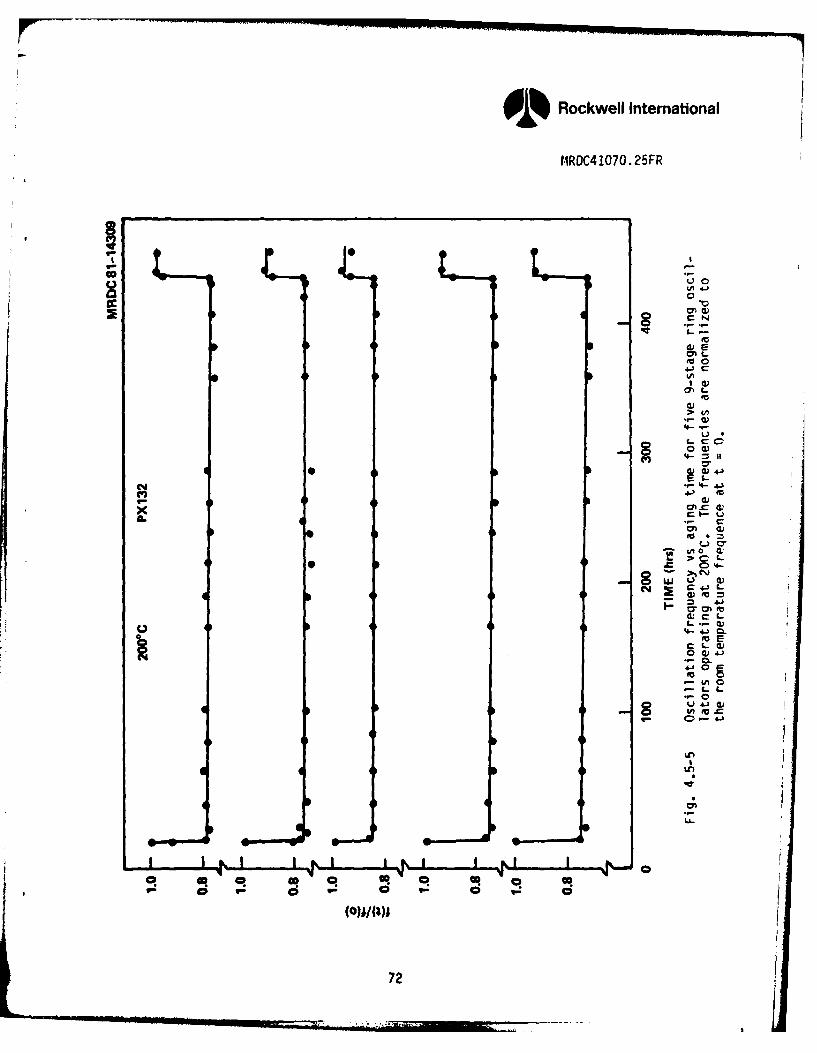
Rockwell International
MRDC4 1070. 25FR
d; ECm t
Lm 0)> C~
C
'.4 a4
~Ln
LA_
OR Ct OR
(OWaW
72U
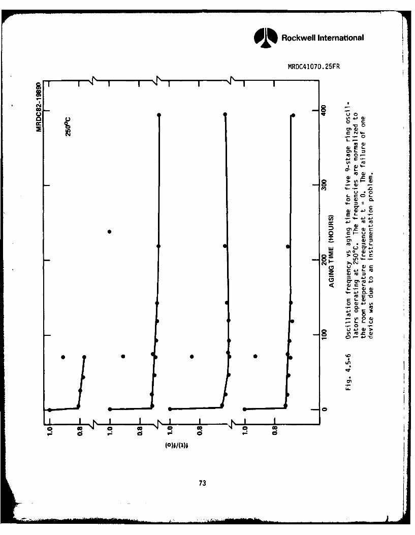
9Rockwell International
MRDC41O7O 25FR
v 0J) a,
LO
4) E
4- --
U CO
- 4JI
EL
a) 4-
m E "(- W
C)
dE dMUM0 4
.~~~i EU .C .0) ...
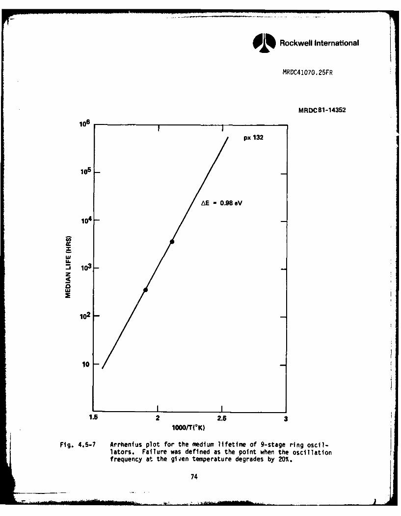
Oi% Rockwell International
MRDC4 1070. 25FR
MRDC 81-14352
106
px 132
AE =0.98 eV
z
102
10
1.5 2 2.5 3IO00O(K)
Fig. 4.5-7 Arrhenius plot for the medium lifetime of 9-stage ring oscil-lators. Failure was defined as the point when the oscillationfrequency at the given temperature degrades by 20%,
74
Rockwell International
MRDC41070.25FR
has been used in all the GaAs digital IC projects at our facility. Conse-
quently, a direct step on wafer (DSW) system was selected and acquired. A
Censor SRA-100 lOX projection aligner was chosen. Figure 4.6-1 shows a photo-
graph of the system. This system is equipped to handle both I inch square
wafers and 3 inch diameter circular wafers, thereby allowing an easy photo-
lithography processing transition to take place.
The Censor DSW was selected because it had the best specifications
and it contained certain features not available on any other equipment. The
specifications of this system are: better than 1 pm resolution; automatic X, Y
and 0 field by field alignment with ±0.1 lim (1a) overlay precision; automatic
focusing; and field by field automatic leveling. This last feature, field by
field leveling, was unique to this system and is particularly important since
the Censor high resolution Zeiss lens has a small depth of focus (I1.5 Pm) by
virtue of its high (0.35 na) numerical aperture. In practice, this local
field-by-field leveling feature eases the flatness specification of the GaAs
wafers, and allows the submicron resolution capability of the lens system to
be utilized effectively.
This Censor DSW equipment can provide repeatable and precisely con-
trolled photolighographic processing. For example, Fig. 4.6-2 shows the
histograms of alignment vernier readings (XTop, XBottom, Y) from 10 wafers
randomly selected for an alignment test. These statistical results confirm
that this equipment is capable of an overlay accuracy of mean +3a of
< 0.25 pm.
Besides the excellent overlay results, resolution patterns surveyed
during the same tests showed resolution consistently lower than or equal to
I pm. The majority (> 50%) of the patterns exhibited - 0.875 pm resolution on
all the wafers surveyed. Figure 4.6-3 illustrates the distribution of pat-
terns resolved as measured from 13 three-inch wafers (416 fields).
The preliminary lithography tests discussed above had been performed
using unprocessed (flat topology) wafers with optimal resist patterns for the
overlay tests. Thus, the first requirement for actual wafer lots was to
define and fabricate alignment marks. These marks must provide maximum edge
75
C5639A/jbs
..... ----
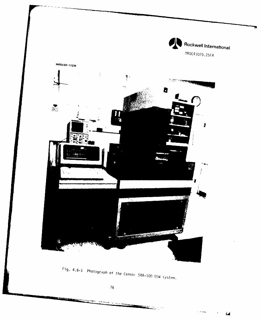
R~ockwell International
MRDC4 1070-25FR
&MRDC82 -17334
Fig. 4.6-1 Photograph of the Censor, SRA.-100 DSW ytr
76
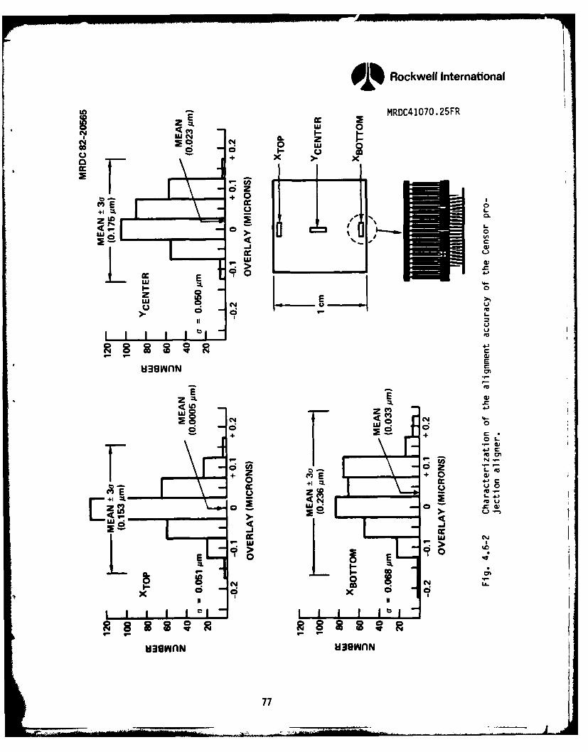
9Rockwell International
w 0 MRDC41O7O 25FR
2 0 L
C., -, + x00
Z LO
+IU CS.,C
9, 0 4
z EQ 6 C
G- IR~E
N < N 40j I d0
d +; C *+ + OL
+ z C4.)+
'44 N X u
ai i e;I
~39WfN ~3Vdfl
77c
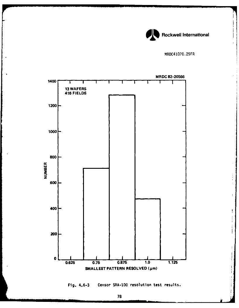
01% Rockwell International
MRDC41070.25FR
MRDC 82-205661400 I 1 1 1
13 WAFERS416 FIELDS
1200
1000
800
n-
z
600-
400-
200 ,
010.625 0.75 0.875 1.0 1.125
SMALLEST PATTERN RESOLVED (pm)
Fig. 4.6-3 Censor SRA-100 resolution test results.
78
Rockwell International
MRDC41070.25FR
acuity as well as maximum contrast in order to obtain the best possible over-
lay precision. After investigating several alignment schemes, titanium metal
embedded between the Si3N4 and SiO 2 layers was chosen as a high yield, high
contact technique. The titanium metal, while maintaining good reflectivity
throughout the process, was also able to withstand the 8500C port implant
anneal. All process steps up to and including the Schottky metal level use
the same alignment marks, and thus level-to-level registration should be
excellent.
As an additional test of resolution capability consistent with actual
wafer processing, a critical dimension experiment was carried out. By mea-
suring the resistance of long metal lines after etching and lift-off, and
plotting the results with respect to known mask dimensions, a measure of line-
width control under actual processing conditions could be obtained. Figure
4.6-4 shows a plot of the length/resistance ratio as a function of various
linewidths on the mask. By extrapolation to zero linelength, a measure of the
replicated error could be determined. Figure 4.6-5 shows the critical dimen-
sion control statistics for the nominal 1.0 pm measurement made on three
wafers. These results are very good, and demonstrate the current capabilities
of the DSW plasma etched lift-off process.
Dry etching techniques, such as the reactive ion etching of SiO 2
layers, are of primary importance. A key element in this process is to sig-
nificantly reduce the erosion of photoresist and Si3N4 while still maintaining
a reasonable SiO 2 etch rate. The use of CHF 3 plasmas was found to be benefi-
cial In this regard; however, the large hydrogen fraction tended to form a
polymer layer on the etched surfaces. The use of CF4 and H2 gas mixtures was
pursued and found to be a much more practical and controllable technique for
etching. As shown in Fig. 4.6-6, the continued addition of H2 tends to sup-
press photoresist erosion while maintaining a high SiO 2 etch rate. The point
of polymer formation was determined to 40% H2 fraction, and consequently, a
standard of 30% H2 was chosen for wafer fabrication in order to provide rea-
sonable process latitude.
A 79
C5639A/jbs
*i ..~ . ......... * . - a
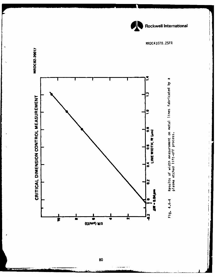
0% Rockwell International
MRDC4 1070. 25FR
3E
z
0.
C WV
zU
z.LUL
'U
LL.
soI
609U.L .j
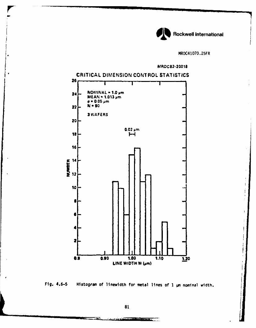
Rockwell International
MRDC41070.25FR
MRDC82-20018
* CRITICAL DIMENSION CONTROL STATISTICS26 1 ...
24 NOMINAL a 1.0 mnMEAN a 1.013 pm*" 0.05 jm
22 N - 90
3 VAFERS
20
0.02
16 -
ic14
12 ,-
10
4I II
0.6 0.90 1.00LINE WIDTH W (.'m)
Fig. 4.6-5 H4istogram of linewldth for metal lines of 1 osn nominal width.
81
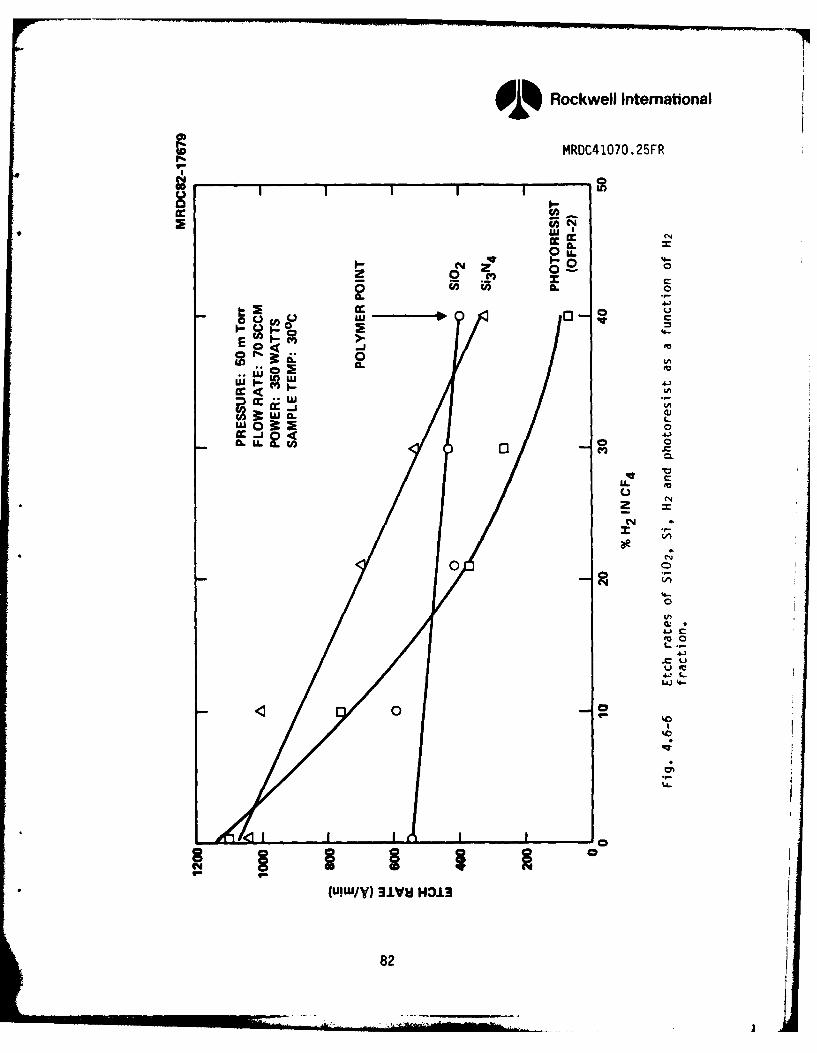
OD Rockwell International
MRDC41O7O .25FR
0 LL1--
z 0CLC
00
E 4-'
0
LO W
03 0
C.,
zN
0 0
N
IUILUY) 31u H=
820
Rockwell International
MRDC41070.25FR
In addition to the etch rate studies, etch uniformity was also inves-
tigated using both the standard LPCVD SiO 2 layer as well as a phosphorus doped
glass (PDG) layer. The results of the measurements are shown in Fig. 4.6-7.
The uniformity of the etch across a 3-in. wafer is very good with both mate-
rials. PSG offers the advantage that its higher etch rate will allow an even
greater selectivity with respect to photoresist loss. Therefore, PSG is a
possible candidate to substitute the LPCVD SiO 2. However, it has not been
incorporated into the mainline process.
In preparation for the launch of the 3 inch wafer process, the uni-
formity of SiO 2 depositions both by sputtering and by low-pressure CVD were
verified, and so was the uniformity of metal depositions both by magnetron
sputtering and e-beam evaporation. As shown by the data in Figs. 4.6-8 and
4.6-9, the uniformity obtained across the diameter of 3 inch wafers is good.
4.7 Fabrication of 3-inch GaAs Wafers
The implementation of the processing of 3 inch wafers was very suc-
cessful. The vehicle chosen was mask set RM3 containing 256 bit GaAs static
RAMs and designed under another DARPA sponsored program.16 The fabrication
process for 3 inch wafers is identical to the process used for 1 inch square
wafers. 1 Differences can be found only in the equipment used. The 3 inch
wafer process required a significant amount of equipment upgrading and re-
placement, the most important item being the photolithography equipment dis-
cussed in Section 4.6.
At the end of this program, 6 lots of 4 wafers each had been fabri-
cated. Breakage was at this stage a rather serious yield limiting factor
causing the loss of 31% of the wafers. However, breakage occurred only at a
few specific process steps, and it was quite clear that significant breakage
reduction was possible by simple Improvements in wafer holding fixtures within
some of the equipment. A reduction of breakage to a still high but acceptable
10% is forecasted. Other causes of catastrophic failures were traced to
dielectric adherence which caused a loss of 6% of the wafers. The yield of
good dies on the wafers was not 100% due to gross misalignment of some dies.
83C5639A/J bs
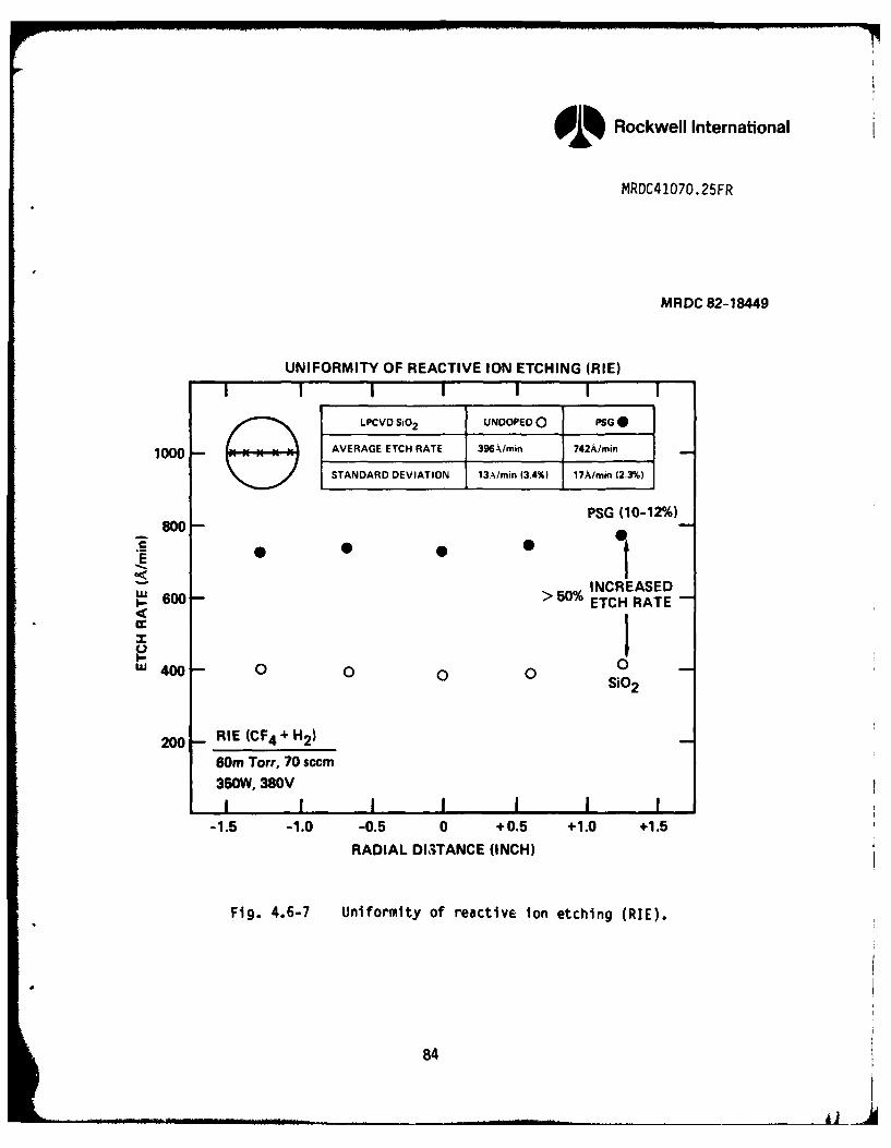
Q % Rockwell International
MRDC41070.25FR
MRDC 82-18449
UNIFORMITY OF REACTIVE ION ETCHING (RIE)
LPCVD Si0 2 UNDOPED 0 PSG 0
1000 AVERAGE ETCH RATE 396,/min 742A/min
STANDARD DEVIATION 13A/main (3.4%) 17A/rin (2.3%)
PSG (10-12%)800
a<INCREASED
600 > 50% ETCH RATE
uJ, 4 00 0 0 0 0 02
200 RIE(CF4 + H2 )60m Torr, 70 sccm350W, 380ViI I I I II ,,
-1.5 -1.0 -0.5 0 +0.5 +1.0 +1.5RADIAL DI3TANCE (INCH)
Fig. 4.6-7 Uniformity of reactive ion etching (RIE).
84
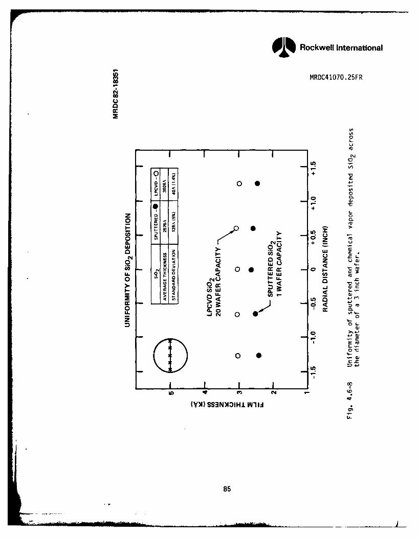
Q%) Rockwell International
MRDC41O7O 25FR
0
LqL
C
0 *-0
z 0)
0 m> LL
0 0
I-W I-- U
0 z, -
o. U' I.-0. N +) U.
o~U 4-) CM 0WW WC.) 4
U)Cu
LOL
00
Ln m NoWO 4-)0)11WI
85 -
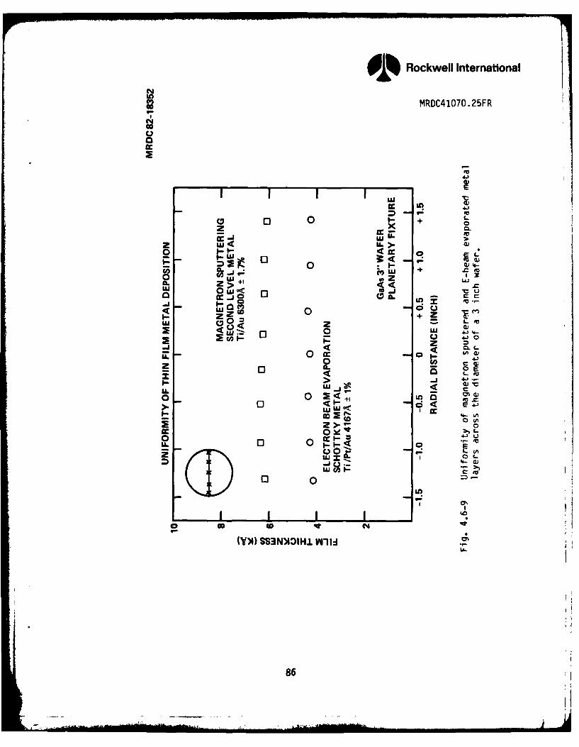
9Rockwell International
MRDC41O7O.25FR
C.,
L'U
0 0 I-+z x
0 W0
0.. 2>w+ +4Lua 0 J13
zj >20 ou12U g C~ C .)
00 z0 < z
C.
Ca z>-
LA. C CLA4
LU C,LL-
U-.
86>
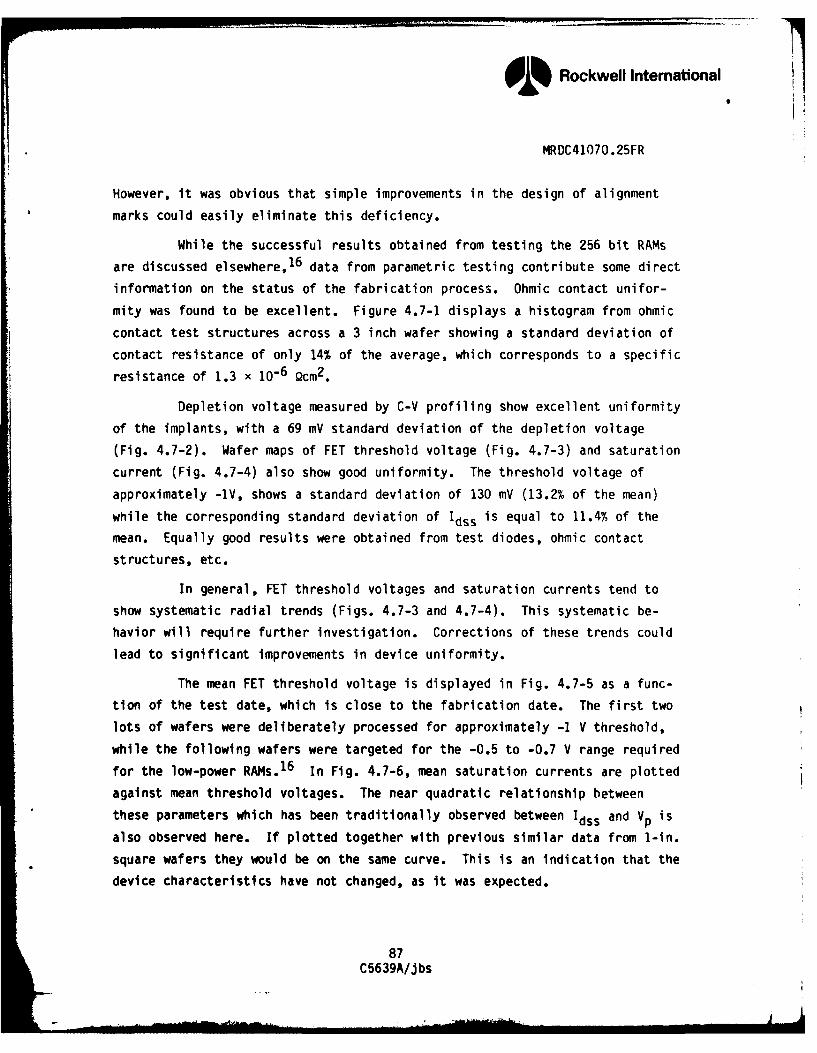
Rockwell International
MRDC41O70.25FR
However, it was obvious that simple improvements in the design of alignment
marks could easily eliminate this deficiency.
While the successful results obtained from testing the 256 bit RAt~s
are discussed elsewhere,16 data from parametric testing contribute some direct
information on the status of the fabrication process. Ohmic contact unifor-
mity was found to be excellent. Figure 4.7-1 displays a histogram from ohmic
contact test structures across a 3 inch wafer showing a standard deviation ofcontact resistance of only 14% of the average, which corresponds to a specific
resistance of 1.3 x 10⁻⁶ Qcm2.
Depletion voltage measured by C-V profiling show excellent uniformity
of the implants, with a 69 mV standard deviation of the depletion voltage
(Fig. 4.7-2). Wafer maps of FET threshold voltage (Fig. 4.7-3) and saturation
current (Fig. 4.7-4) also show good uniformity. The threshold voltage of
approximately -1V, shows a standard deviation of 130 mV (13.2% of the mean)
while the corresponding standard deviation of Idss is equal to 11.4% of the
mean. Equally good results were obtained from test diodes, ohmic contact
structures, etc.
In general, FET threshold voltages and saturation currents tend to
show systematic radial trends (Figs. 4.7-3 and 4.7-4). This systematic be-
havior will require further investigation. Corrections of these trends could
lead to significant improvements in device uniformity.
The mean FET threshold voltage is displayed in Fig. 4.7-5 as a func-
tion of the test date, which is close to the fabrication date. The first two
lots of wafers were deliberately processed for approximately -1 V threshold,
while the following wafers were targeted for the -0.5 to -0.7 V range required
for the low-power RAMs. 6 In Fig. 4.7-6, mean saturation currents are plotted
against mean threshold voltages. The near quadratic relationship between
these parameters which has been traditionally observed between Idss and V p is
also observed here. If plotted together with previous similar data from 1-in.
square wafers they would be on the same curve. This is an indication that the
device characteristics have not changed, as it was expected.
87C5639A/Jbs
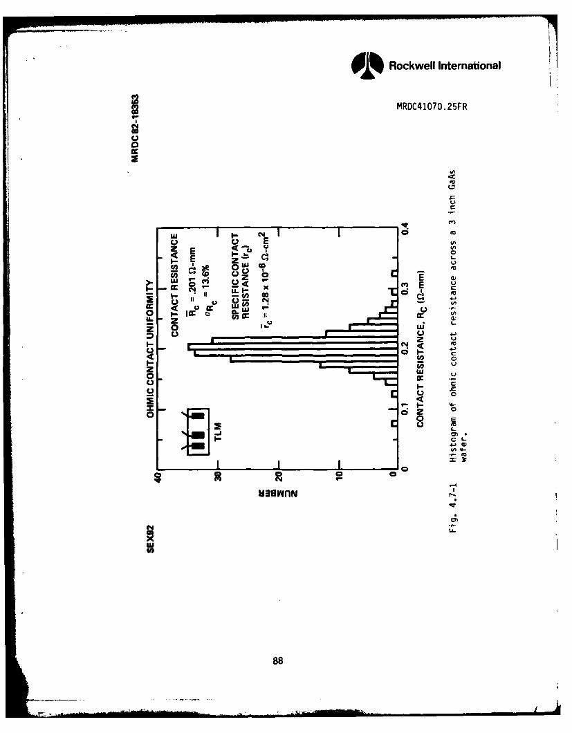
Rockwell International
MRDC41O7O. 25FR
UUI00
Z EU
C: UC
z E2 9 4% C14 x
Co4
U.U
I N4 < U
U0ICIO
z U00
ZN M0 E
CC
I-L
88Y~fl
Rockwell International
MRDC41070.25FR
(N
LU 4-
> 00t
> C-W 0. 4 --
4.. 4J0
C C
> >: >= C +
Ln~
COa CO
D E 4..-
• " mm:,,. GN8g
___ ___ ___ __ ___ ___ ___ __Cm MtL
NC 0
C 4J 4)
C>CCif~~ CC W
>>>>~ I
iuCu
89
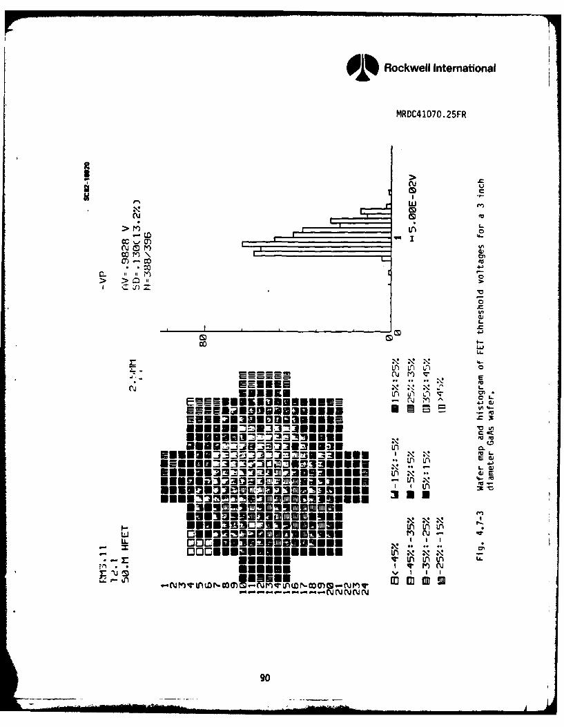
0 % Rockwell International
MRDC4 1070. 25FR
I>C'j
u 0 m
CLL
>rr) LA)orzj r -
U-))
U')~ \nUM N a
"II 0X1 .
900
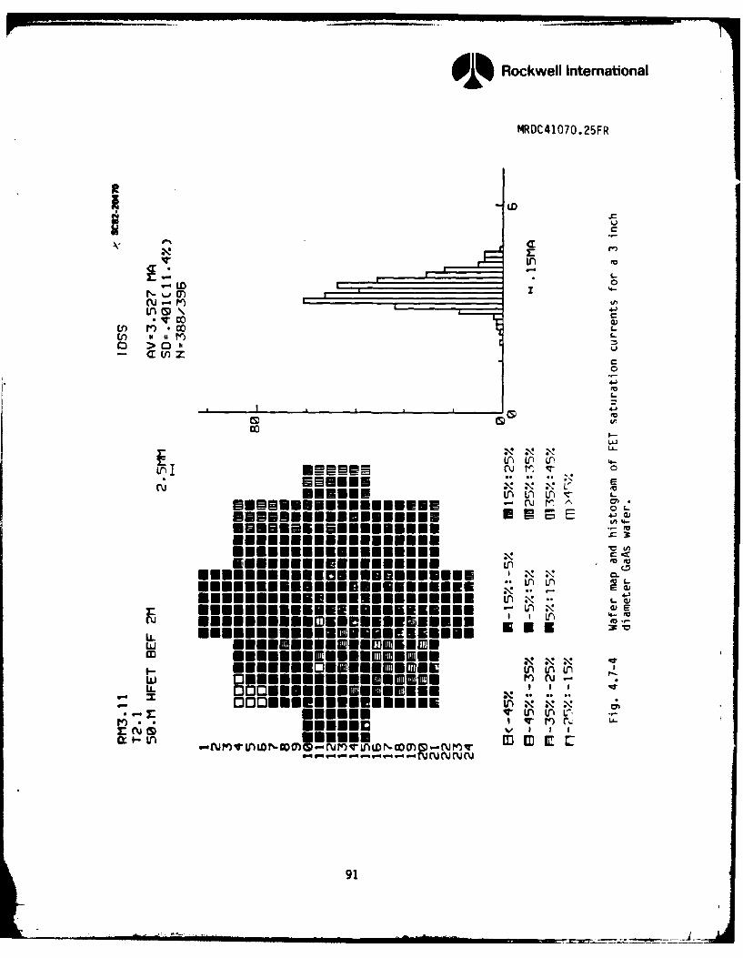
i Rockwell International
'4RDC41070.25FR
<r U)
LDL
COC
c0 > ofC V) z
G0
GoL
. rntrM
U 9 G E
C CrE**.m~mEU.toE.to
*EEUEEEUEUEE.U.UUZ Xn M
r *f********EEfl5*Efl* U') fuUUEEEEUUWUU0EEEEUEEE*EUUEUUUUUUEEEEEUE
*EUUUUEWUULWuuuoinuuuIUUEUEUUIDE
-~~~L InUUUEUIEUUnDOEUEEEUEEWU. xL
-- 91
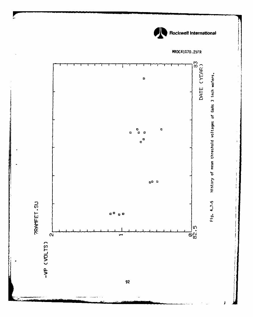
Rockwell International
MRDC41070-25FR
u-
u .
<1.
ri a 0
0
DO 0
0))
G)C..
C*
00
(LC
>)
920 0
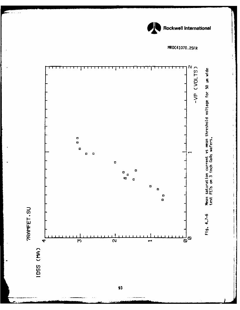
9D Rockwell International
MRDC4 1070. 25FR
111111~~~131 I1 I 1 1 1 1 1 II 1 l I I 1 1
(F339
C-t13i
C.13 r
0
CA
(n)
W.
<1aU I I L L -1 f i l 1 1 1 1 1 1 1 1 1 1 1 1 1 1 1 1 1 1 1 1 1 1
'IrV) ~ jM-4(S)(S
r" IUa a'-
WU
WE
930
9 Rockwell International
MRDC41070.25FR
In conclusion, the launch of the 3 inch wafer process was very suc-
cessful. A number of second order problems such as breakage, alignments, etc.
have been identified, and ideas on how to address them have been generated and
proposed for a new phase of this program.
94C5639A/Jbs

9L Rockwell International
MRDC41070.25FR
5.0 CIRCUIT DESIGN AND TEST
Although the main emphasis of this program was on process develop-
ment, design and testing of GaAs integrated circuits was also an important
task. All the work reported here was carried out using normally-on MESFET de-
vices using Schottky Diode FET Logic (SDFL) gates as circuit building blocks.
In the early part of the program, the evaluation of 8 x 8 bit parallel multi-
pliers (1000 gate circuits) developed and fabricated under a previous program
was completed. The circuit was found completely functional, and a best multi-
ply time of 5.2 ns was determined. Since these results were discussed in the
previous final report, 1 they are not repeated here. A new logic family called
Schottky Diode Diode FET Logic (SD2FL) which represents an expansion of SDFL
was developed and evaluated. This work, discussed in Section 5.1, indicated
that this new family can be very useful, but only for limited applications.
Sequential circuits of the programmable pattern generator type were designed
and tested (Section 5.2). Finally, the design of a family of mask program-
mable logic array meeting ERADCOM requirements was started. This activity,
discussed briefly in Section 5.3, and more extensively in Appendix A, is
expected to lead to the development of components for a frequncy synthesizer.
5.1 Schottky Diode-Diode FET Logic (SD2FL)
A logic gate circuit design must be capable of extension to two or
more levels of logic per gate delay in order to realize the highest speed, and
to minimize chip area and power dissipation for a given IC logic technology (a
logic level consists of one (N)AND or (N)OR operation of arbitrary width).
Multilevel gate implementations allow complex logic operations to be achieved
in slightly over one basic logic gate propagation delay (Td) rather than two
or three delays as would be the case for single level NOR or NAND implementa-
tions. They also dissipate less power and require less wafer area than single
level circuit implementations.
The use of combinations of series (NAND) or parallel (NOR) FET con-
figurations to achieve two-level logic functions is common. VanTuyl, et al. 17
demonstrated depletion-mode GaAs MESFET buffered-FET logic (BFL) NAND/NOR (or
95C 5639A/J bs
Rockwell International
MRDC41070.25FR
NAND/WIRED-AND) gates, with up to two NAND input terms (series or dual-gate
FETs) and up to two of these NAND functions "drain dotted" together, having
propagation delays as low as 'd = 110 ps. Multi-level logic gate configura-
tions may also be realized in SDFL with up to 3-level gates.18 In the pre-
viously-published SDFL work, 18 the FET logic function utilized was principally
the inverter, so that, with the diode-OR, a NOR gate function was realized
(Fig. 5.1-1a). On the other hand, by using such diode-OR clusters on each
gate of a dual gate FET (or series-FET connection), an OR/NAND 2-level gate is
achieved (Fig. 5.1-1b), This gate is the complement of the 2-level NAND/NOR
gate realized in BFL, except that the number of first level terms in the SDFL
version is no longer restricted to two. The resulting OR/NAND function
F = (A+B+C)(D+E+G) can be used to reduce considerably the propagation delay
per equivalent gate by performing a two-level operation in approximately one
NOR gate delay. Power dissipation is only slightly above that of a NOR delay
gate (one added pull-down) and the area is also only slightly greater.
A three-level (OR/NAND/WIRED-AND) gate can also be constructed by the
use of "drain-dotting" or sharing of a common pull-up by two OR/NAND gates.
An example of this gate is shown in Fig. 5.1-ic. Again, the number of OR inputs
is arbitrary. Here, the three-level logic function F = [(A+B+C) (D+E+G)] +
[(H+I+J) (K+L+M)] is performed by this gate in substantially the same propa-
gation delay time required by a single NOR gate. Proper dissipation is again
only slightly above that of a single level (NOR) gate, and the area would be
about twice that of a NOR gate.
The multi-level logic gate approach described above allows major
saving of chip area and power dissipation, and also increased circuit speed
(fewer gate delays). In general, however, the numbers of terms which can be
practically "NAND'ed" with series FETs without substantial performance degra-
dation Is limited to two due to parasitic gate capacitances and FET "ON"
resistances. Similar restrictions apply to the "drain dot" -wired AND of the
three level OR/NAND/WIRED-AND gate. To avoid this fanin restriction of multi-
level logic gates, the extra fast logic element available in the GaAs Schottky
diode can be utilized to perform two levels of logic operations rather than
just one level. Figure 5.1-2 illustrates the use of 2 levels of diode logic
96C5639A/jbs
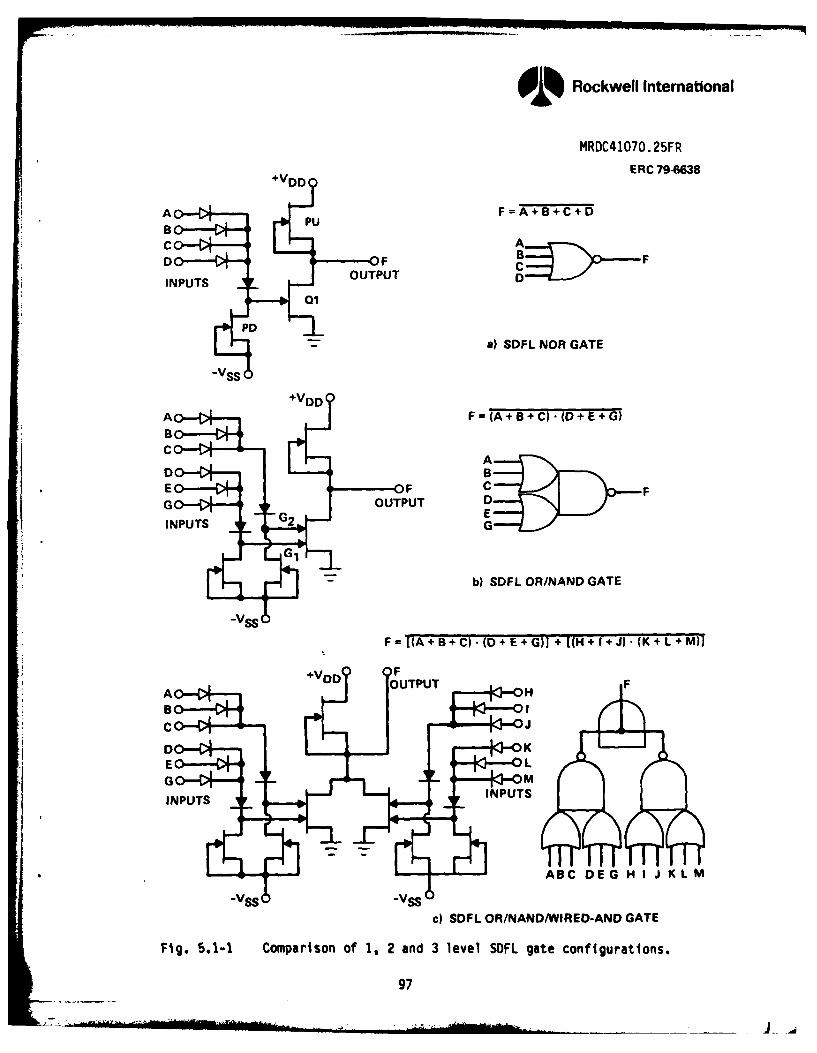
91 Rockwell International
MRDC4 1070. 25FR
ERC 79-663+VDD
A F=A+B+C+D8 Pu
cc
INPUTS OUTPUTD01
~PDa) SDFL NOR GATE
-VS5
A F=(A +B +C) -(D +E +G)BC
A
E F CFGOUTPUT D
G2 E
F = (A + B + C)- (D + E + G) I + I((H + I + J) (K +L4 M)]
A +VDD OUTPUT HF
C .
-ABC DEGNHI J K LM
c) SDFL OR/NAND/WIRED-AND GATE
Fig. 5.1-1 Comparison of 1, 2 and 3 level SDFL gate configurations.
97
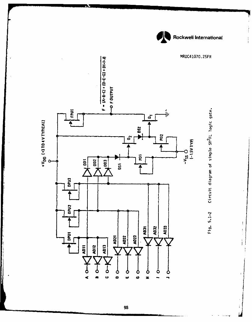
Rockwell International
MRDC41O7O .25FR
ILE-
CI-)
pp C
E
C44
98
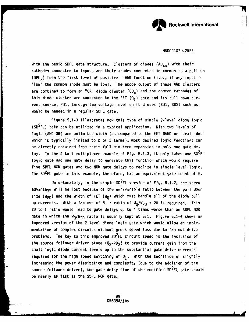
Rockwell International
MRDC41070.25FR
with the basic SDFL gate structure. Clusters of diodes (ADxx) with their
cathodes connected to inputs and their anodes connected in common to a pull up
(DPUx) form the first level of positive - AND function (i.e., if any input is
"low" the common anode must be low). The anode output of these AND clusters
are combined to form an "OR" diode cluster (ODx) and the common cathodes of
this diode cluster are connected to the FET (Q1 ) gate and its pull down cur-
rent source, PD1, through two voltage level shift diodes (SO1, SD2) such as
would be needed in a regular SDFL gate.
Figure 5.1-3 illustrates how this type of simple 2-level diode logic
(SD2 FL) gate can be utilized in a typical application. With two levels of
logic (AND-OR) and unlimited width (as compared to the FET NAND or "drain dot"
which is typically limited to 2 or 3 terms), most desired logic functions can
be directly obtained from their full min-term expansion in only one gate de-
lay. In the 4 to 1 multiplexer example of Fig. 5.1-3, it only takes one SD2FL
logic gate and one gate delay to generate this function which would require
five SDFL NOR gates and two NOR gate delays to realize in single level logic.
The SD2FL gate in this example, therefore, has an equivalent gate count of 5.
Unfortunately, in the simple SD2FL version of Fig. 5.1-2, the speed
advantage will be lost because of the unfavorable ratio between the pull down
size (WpD) and the width of FET (WQ) which must handle all of the diode pull
up currents. With a fan out of 6, a ratio of WQ/WpD = 20 is required. This
20 to 1 ratio would lead to gate delays up to 4 times worse than an SDFL NOR
gate in which the WQ/WpD ratio is usually kept at 5:1. Figure 5.1-4 shows an
improved version of the 2 level diode logic gate which would allow an imple-
mentation of complex circuits without gross speed loss due to fan out drive
problems. The key to this improved SD2FL circuit speed is the inclusion of
the source follower driver stage (Q2-PD2) to provide current gain from the
small logic diode current levels up to the substantial gate drive currents
required for the high speed switching of Q1. With the sacrifice of slightly
increasing the power dissipation and complexity (due to the addition of the
source follower driver), the gate delay time of the modified SD2FL gate should
be nearly as fast as the SDFL NOR gate.
99C5639A/J bs
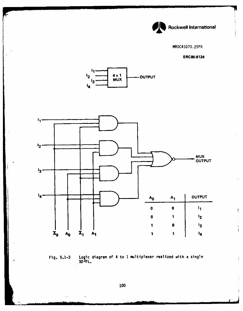
Rockwell International
MRDC41070.25FR
ERC80-8124
12 - 4x1 OUTPUT13O MUX
14
12
MUXOUTPUT
13----
14 A0 A1 OUTPUT
0 0
0 1 12
1 0 13
A0 A0 1 A1 1 1 14
Fig. 5.1-3 Logic diagram of 4 to 1 multiplexer realized with a singleSDFL.
• 100
Rockwell International
MRDC41O7O 25FR
ERC 80-8777
AA
B8
C F (OUTPUTD G ( IJ
DD
EE
0 -
H 0
(-1.5V TYP)
Fig. 5.1-4 Schematic of an improved version of the Schottky diode-diode FETlogic (SD2FL) gate.
101
94L Rockwell International
MRDC4107O.25FR
The extension of this SD2FL approach to an even higher level of logic
function can be easily achieved. Note that if Q is a dual gate FET and if
the input and same source follower structure is used for each gate, a 3 level
gate AND/OR/NAND gate will be obtained. Similarly, if another such 3 level
gate were connected with their outputs sharing a common pull up, a 4 level
AND/OR/NAND/ WIRED-AND would be obtained.
An 8 x 8 bit parallel multiplier was chosen as a vehicle to test
SD2FL. The architecture is the same simple ripple type previously used with
SDFL: so that conclusions could be drawn about the efficiency of the SD2FL
approach compared to the SDFL approach. The 8 x 8 multiplier was designed
using two-level, Schottky Diode-Diode FET Logic (S02FL) gates to implement the
adders in the multiplier array. The compelling feature of these gates is that
a full adder cell implemented with four of them provides both sum and carry
outputs with a propagation delay equal to only one gate delay (Td), rather
than the average 2.5 Td of a SDFL full adder. The circuit structure of the
SD2FL gate is slightly more complex than that of a SDFL gate, resulting in a
1d for a SD2 FL gate that is approximately 1.5 times that of a SDFL gate. This
is a result of the increased capacitance due to more diodes at the logic sum-
ming mode, and the delay of the additional source follower stage used to dis-
charge the gate of the switching FET. Therefore, the speed advantage of the
SD2FL adder, compared to an (average) SDFL adder, is on the order of 1.7
times.
Preliminary estimates were previously made of the packing density and
power dissipation of a SD2FL multiplier that would achieve this increase in
speed. These preliminary estimates indicated that along with the increase in
speed, there would result a decrease in layout area, as well as a decrease in
power dissipation. However, the detailed circuit design and layout performed
for the multiplier established that the reduction in area for the 1 -d adder
is not as much as estimated earlier, and that the power dissipation is sub-
stantially greater when appropriate transistor sizes are selected for the in-
creased speed (compared to the NOR gate SDFL implementation). With the design
102C5639A/jbs
Oil Rockwell International
MRDC41O7O .25FR
essentially complete, size and power estimates resulted as follows: 1) the
size of a SD2FL full adder is approximately 90% of that of a SDFL adder; 2)
its power dissipation, which, unlike that of the NOR adder, is constant,* will
exceed the average power of a NOR adder by 92% (or 1.92 times), and will ex-
ceed the maximum power of a NOR adder by 35%; 3) additionally, relat've to
size, the increased power dissipation necessitates an increase in power bus
line areas that nearly cancels the 10% area saying when equal current densi-
ties are maintained. These figures apply while realizing the estimated 70%
increase in speed. A one-line summary is that the SD2FL multiplier realizes a
1.7 times increase in speed, less than 10% saving in chip area, with nearly
twice the power dissipation of a NOR implementation.
At this point, it is worth considering the discrepancy between expec-
tation and realization of area and power. When the completed design is exam-
ined, it becomes clear that an array multiplier circuit benefits less than
almost any other logic circuit from a S02F implementation, compared to a
straight NOR (SDFL) one. The predominant reason is that both true and comple-
ment values of the sum and carry outputs of each adder must be both generated
and routed as interconnections in implementing full adders. Thus, the gate
count is increased, as well as the routing area. S2F gates are larger than
SDFL gates, in order to drive the greater capacitance of the greater number ofinput diodes; also, to assure switching under worst case conditions, it is
necessary to increase the sizes of the input diodes, further increasing input
capacitance and, hence, gate size.
Of the four gates that generate the sum and carry and their comple-ments, clearly two must always be "on." The power dissipation is not only
constant, but equal to that of the larger gates. The net result is the mini-mal benefit in area and penalty in power mentioned above.
*The power is constant because for each of the sum and carry outputs, both trueand complement are provided; thus one and only one gate of each pair isalways on.
103C5639A/J bs
Rockwell International
MRDC41O7O.25FR
The conclusion is that the AND-NOR combination is not very efficient
for arithmetic functions. The basis of arithmetic is the exclusive-OR func-
tion. Implementing an exclusive-OR with a minterm expansion in the S02FL gateinvolves the maximum number of combinations of true and complement variables;
e.g., for three variables, the sum output is
S = ABC + ABC + ABC + ABC (2)
None of the reductions ordinarily encountered in the case of more
general logic functions is possible. Thus, in terms of interconnections and
numbers of inputs, the adder array used in the multiplier is one of the most
complex circuits that could be selected for implementation with S02FL gates.By comparison, the SDFL NOR gate implementation is a fairly efficient one;
only two (true) outputs are generated, minimizing interconnect area and the
number of driver gates. The input fan-in is low, so that driver gates are
small. Thus, the area and power of the AR5 SDFL multiplier have been mini-mized for an implementation that is efficient in terms of those (area and
power) parameters. This efficient application of the NOR gates is being com-
pared to a much less efficient implementation with SD2FL gates. If a compari-
son were made with an SDFL version in which true and complement of sum and
carry outputs were generated and routed (so that the comparison would be for
functionally equivalent circuits), the area and power savings of Sfl2FL would
be obtained. The area and power savings should also apply when implementing
logic functions other than arithmetic.
As an example of a circuit that is efficiently realized with SO2FL
gates, consider the multiplexer circuit discussed earlier in this section and
shown on Fig. 5.1-3. It can be implemented with one SD2FL gate, or 5 SDFL NOR
gates. Area and power savings for this example are dramatic. The area of aSD2FL gate is approximately 4500 Wj2, or 46% of the 9600 Mn2 occupied by a 5
gate equivalent. The power dissipation of the one SO2FL gate in only 40% of
the power in a 5 gated equivalent, when equal loading is considered.
104C5639A/Jbs
9Rockwell International
MROC4107O *25FR
* The 8 x 8 multiplier was digitized with the same peripheral latchcircuits that were used on the previous SDFL multiplier. A photograph of the
chip is shown on Fig. 5.1-5.
The full 8 x 8 multiplier was a very complex and large chip, whichhas the following impact on testing. First, the bias sensitivities of the twotypes of gates (SD2FL and SDFL) were expected to be slightly different. Sec-
ondly, the yield on such large chips was anticipated to be low enough that aconsiderable number of chips would need to be tested to find fully functionalones. This testing would be made more difficult by the uncertainty of properbias voltage conditions.
To overcome these potential testing limitations, the multiplier wasdesigned with an alternate second metal mask that eliminated the latches, and
subdivided the array into four smaller arrays (two 4 x 4 and two 3 x 4
arrays). This alternate connection layer would be used on the first lots of
wafers to facilitate testing on the smaller S2F arrays, which should have
higher yield of working arrays, with outputs directly measurable so that biasvoltage effects could be observed. Later lots would be processed with the
fully connected mask layer.
Testing was started by checking a few circuits for functionality,using a ripple test, while adjusting voltages. From these, a number wereidentifiled that had no shorts, showed some degree of functionality, and ex-
hibited output waveforms with well defined voltage levels. These were then
tested in more detail, using the lower order bits in the upper right-hand
corner. In Fig. 5.1-6 a functional diagram of the upper right corner, and theelements involved are shown. Specifically, the gate that combines a0 and b0to form the LS8 of the product, P0 is a SDFL gate, so that SDFL performancecan be evaluated. The gates and adders that form P1 and P2 are completelyS02FL. The number of data paths is limited, so that correct operation can be
verified; there are 32 unique combinations for this adder circuit. Uinfor-
* tunately, under testing, it was found that lack of access to circuit nodesmake it difficult to identify specific faults. For example, P1 is the sum
105C5639A/J bs
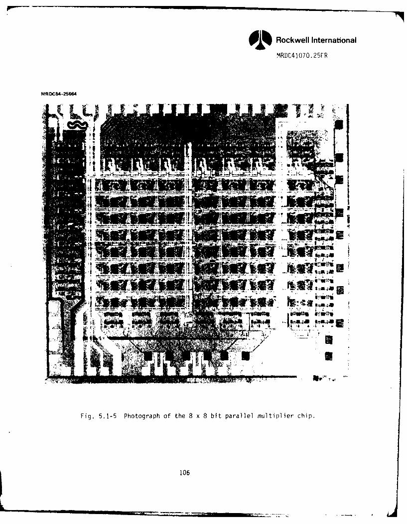
Rockwell International
MRDC41O70.25FR
MRDC84-25664
1061
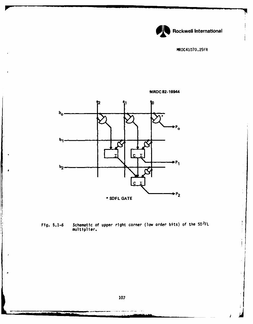
0L Rockwell International
MRDC41070.25FR
MRDC82-19944
12 a
p0
C
• c _
b22
* SDFL GATE
Fig. 5.1-6 Schematic of upper right corner (low order bits) of the SD2FLmultiplier.
107
01% Rockwell International
MRDC41070.25FR
output of a single field adder; its operation can be verified for the sum, but
not for the carry. Similarly, the other adders are not fully accessible.
The adder corner combination was tested on several chips, for all
input combinations, with varying bias conditions. The chips tested were
selected for well defined output levels. None of the chips'functioned com-
pletely. The failure were not consistent between input combinations; in some
cases, for example, several combinations would produce an erroneous output
only if a single gate had failed, but several other combinations would produce
outputs that required that same gate to function. The testing was carried out
to the point where it was suspected that voltage variations within the circuit
during operation were affecting operation of some gates.
Testing of SD2FL gates on previous mask sets has shown that the SD2FL
gate can operate as designed. The testing on AR6 has shown that an SD2FL
adder also operates. It is evident that cascading them results in interac-
tions that have not been considered in the design. It is suspected that de-
sign and layout changes made with the intention to improve performance may be
related to the failures.
Since the revised performance predictions discussed earlier did not
indicate sufficient advantages for the SD2FL design over a simple SDFL rilti-
plier, efforts to further investigate the cause of the failure were not
continued.
In conclusion, the SD2FL gate can be implemented (despite the lack of
success with the SD2FL multiplier). However, it is advantageous only in cer-
tain specific cases where its large ANDing capability can be exploited. This
is the case in the low-power GaAs static RAM, where SD2FL gates were success-
fully used in the address decoder circuits.19 However, a widespread use of
SD2FL circuits, as it was attempted on the 8 x 8 bit multiplier, is not
advisable.
108C5639A/jbs
Rockwell Intemational
MRDC41070.25FR
5.2 Sequential Circuits
A programmable linear feedback shift register (LFSR) was selected as
a demonstration circuit because of important potential system applications.
This circuit produces a binary sequence of length 2m-1 , where m is the number
of stages. There are 2m-1 possible initial loading conditions where each
loading results in a distinct output sequence. Binary linear feedback shift
registers can also be used to perform polynominal division, where all polynom-
inals have coefficients that are either one or zero. When a linear feedback
shift register (LFSR) is used for division, its feedback connection polynom-
inal is defined as the divisor polynominal. To perform division, the regis-
ters in the LFSR should be cleared to zero. Then the polynominal to be
divided is fed sequentially into the input of the LFSR with the most signifi-
cant coefficient first. The quotient polynominal appears at the output of the
LFSR as the input polynominal is being divided. After the input polynominal
has been entered into the LFSR, the remainder polynominal or residue is left
in the shift register stages.
A programmable shift register/pattern generator was designed on the
same mask set (AR6) used for the 8 x 8 bit SD2FL multiplier (Section 5.1).
The circuit generates an m-sequence (m = 7 or 8) P/N code or performs poly-
nomial division. When used as a binary m-sequence code generator, the m stage
shift register with feedback polynomial generates a distinct output sequence
for each of the 2m-1 possible initial conditions. The shift register is con-
figurable in order to generate two distinct m-sequences. For m = 7, the seven
stage shift register has a feedback polynomial of x7 = x3 + 1, and is capable
of generating a binary P/N code of length 27 - I = 127. For m = 8, the eight
stage shift register has a feedback polynomial of x8 = x4 + x3 + x2 + 1, and
is capable of generating a binary P/N code of length 28 - 1 = 255. By using
the two synchronized shift registers, whose lengths are relatively prime and
whose feedback polynomials are different, a gold-code sequence with a period
of (27 - 1)(28 - 1) can be generated with the addition of an exclusive-OR
output gate.
109C5639A/jbs
Rockwell International
14ROC41O7O.25FR
When used to perform polynomial division, the mn stage shift register
should be first cleared to zero. The polynomial to be divided is fed sequen-
tially into the shift register with the most significant coefficient first.
The quotient polynomial appears at the output of the shift register as the
input polynomial is being divided. After the input polynomial has been
entered into the shift register, the remainder polynomial is left in the shift
register stages. In the division mode, the shift register divides by 1 + x3 +
x7 for mn - 7 and by 1 + x2 + x3+ x4+ x8 for mn = 8.
There are three design options for the programmable shift register!
pattern generator including the direct form realization, and two forms of
transpose realization. The direct form realization was chosen due to the
minimum level of gate delays in the feedback connections. Figure 5.2-1 shows
the logic diagram of the direct form realization of the programmable shift
register/pattern generator. The seven and eight stage shift register/patterngenerator in the AR6 mask set are designed as two individual circuits, andeach contains two control lines to provide the four distinct modes of opera-
tion. The two pattern generators are configured in pairs on the same chip so
that they can feed through a single EOR gate correlation output circuit to
produce a gold-code of (27 _ 1)(28 - 1) bit long. They are also capable of
operating independently in different modes.
Figure 5.2-2 shows the logic diagrams of a double clocked OR/NAND
master slave flip-flop which is used to implement the register stages. It was
chosen over a D-f lip-f lop type due to the speed performance requirement for 1-
2 GHz clock frequency. The OR/NAND master slave flip flop has a maximum oper-
ating frequency of 1/2.3 To while the NOR implemented 0 flip flop requires 1/5
10. SDFL NOR gates are used to implement the EOR logic between shift register
stages. Figure 5.2-3 and Figure 5.2-4 show the equivalent logic diagrams of
* the seven and eight stage shift register/pattern generator, respectively.
Circuit simulations of the double clocked OR/NAND master slave flip* flop revealed that its speed performance was critically sensitive to the duty
cycle of the two clock inputs and the relative phase shift between CK
110C5639A/Jbs
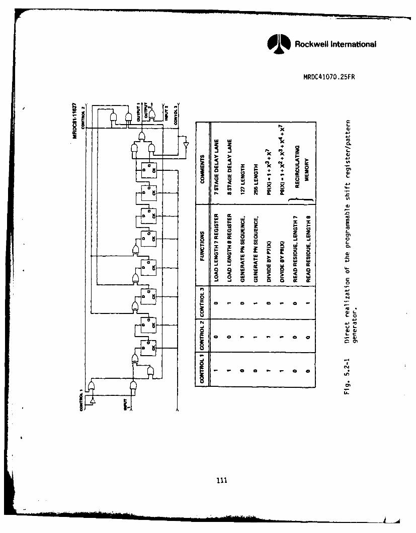
OD~ Rockwell International
MRDC4 1070. 25FR
X 4)+ +"
Mi W
U U Wi ' z z M4r ..j
m. i
Uz z
Z~ ~ ~ Z 2
OC 2 2 oMi W i M
Fi
0 0 a a4
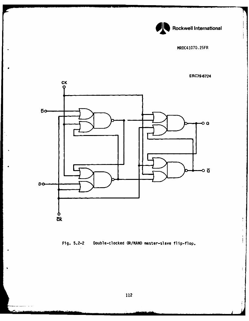
Rockwell International
MRDC4 1070. 25FR
ERC79-6724CK
Fig. 5.2-2 Double-clocked OR/NAND master-slave flip-flop.
112
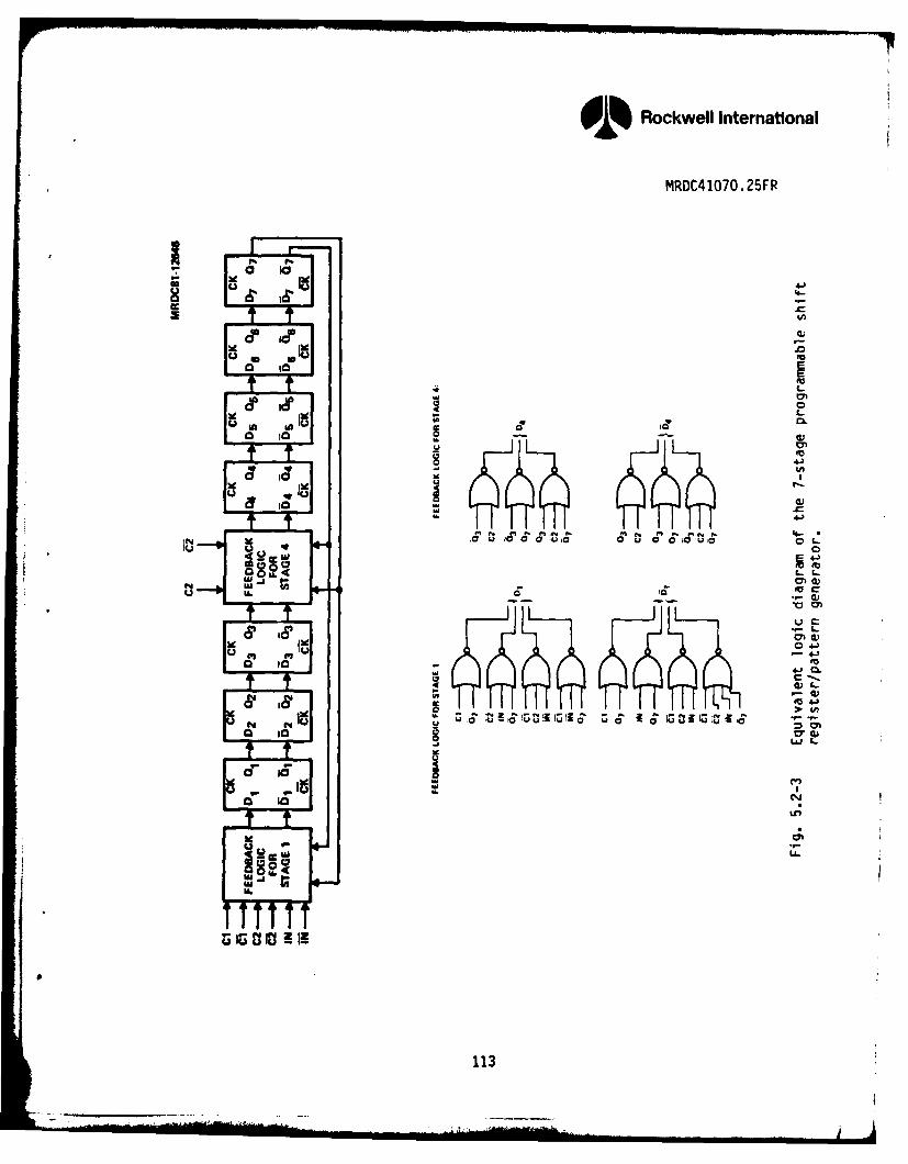
9D Rockwell International
MRDC41070.25FR
i I1L) , .-.
4-
UUQ
U
C* L.
CAC
4- ', , 0-
113
-o 1 1 M0 gUI, ... . . ' . .
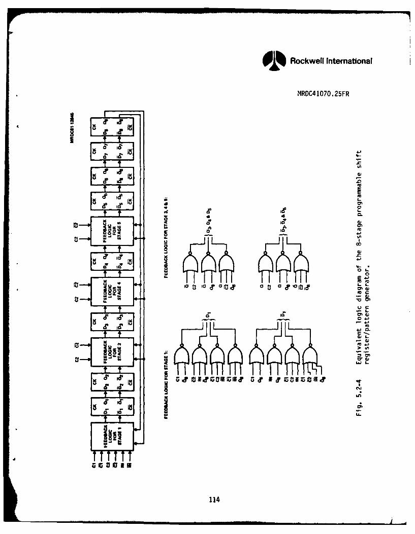
9 Rockwell International
MRDC41070.25FR
eif lie .
5 + '-'-"+ A
CIwm m
cc Im cu t--Juu 1)(0 a,-C
g ,a Ia ,,=
w -L
.,
u CC
16 01 0*I
114j
Cr~~~ 0) 4
111
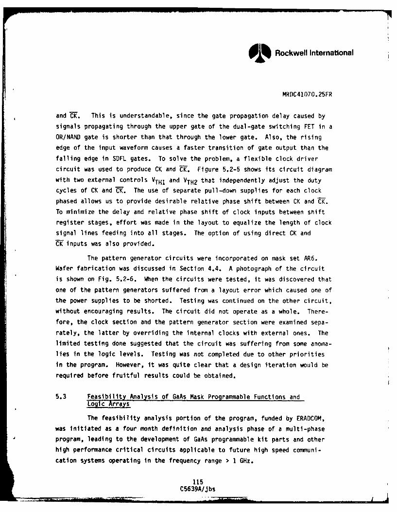
Rockwell International
MRDC41O7O. 25FR
and TK- This is understandable, since the gate propagation delay caused by
signals propagating through the upper gate of the dual-gate switching FET in a
OR/NAND gate is shorter than that through the lower gate. Also, the risingedge of the input waveform causes a faster transition of gate output than the
falling edge in SDFL gates. To solve the problem, a flexible clock drivercircuit was used to produce CK and C. Figure 5.2-5 shows its circuit diagram
with two external controls VTHI and VTH2 that independently adjust the dutycycles of CK and TK. The use of separate pull-down supplies for each clock
phased allows us to provide desirable relative phase shift between CK and ZK.
To minimize the delay and relative phase shift of clock inputs between Shift
register stages, effort was made in the layout to equalize the length of clock
signal lines feeding into all stages. The option of using direct CK andTK inputs was also provided.
The pattern generator circuits were incorporated on mask set AR6.Wafer fabrication was discussed in Section 4.4. A photograph of the circuit
is shown on Fig. 5.2-6. When the circuits were tested, it was discovered that
one of the pattern generators suffered from a layout error which caused one ofthe power supplies to be shorted. Testing was continued on the other circuit,
without encouraging results. The circuit did not operate as a whole. There-
fore, the clock section and the pattern generator section were examined sepa-rately, the latter by overriding the internal clocks with external ones. Thelimited testing done suggested that the circuit was suffering from some anoma-
lies in the logic levels. Testing was not completed due to other priorities
in the program. However, it was quite clear that a design iteration would be
required before fruitful results could be obtained.
5.3 Feasibility Analysis of GaAs Mask Programmable Functions and
Logic Arrays
The feasibility analysis portion of the program, funded by ERADCOM,
was initiated as a four month definition and analysis phase of a multi-phaseprogram, leading to the development of GaAs programmable kit parts and otherhigh performance critical circuits applicable to future high speed communi-
cation systems operating in the frequency range >1 GHz.
115C5639A/Jbs
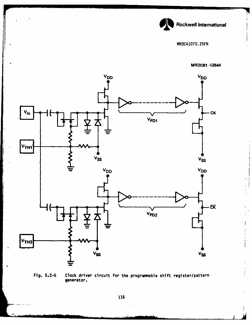
91 Rockwell International
t4RDC41O7O 25FR
MRDC81 -12644
VDD VDD
Vin CK
VPD1
V'SVSS
VDD VDD
Ll VPD2
Fig. 5.2-5 Clock driver circuit for the programmnable shift register/patterngenerator.
1 16
Rockwell International
MRDC4 1070. 25FR
MRDC84-25665
Fig. 5,2-6 Photograph of the 7-,stage and 8-stage pattern generator chips.
117
9 Rockwell Intemational
*m MRDC41070.25FR
A brief outline of the program and results follows. For complete
details of the study phase, refer to Appendix A which is included as part of
this final report.
During Phase I, a study of the various design approaches to GaAs was
performed to determine which would be best suited to the particular applica-
tion. For instance, Schottky diode-FET logic (SDFL), direct coupled logic
using enhancement-mode MESFETs, buffered FET logic (BFL), and other circuit
approaches were analyzed based on maximum speed, speed vs power and size vs
speed/power. The conclusion from this analysis was that BFL was the most
suitable candidate for implementing the various circuit functions.
A list of candidate circuits/functions which would be incorporated
within the cells was developed through a coordinated effort between MRDC
(Rockwell Microelectronics Research and Development Center (Anaheim, CA)) and
CTPD (Rockwell/Collins Telecommunications Products Division (Cedar Rapids,
IW)) personnel. Upon completion of the list, it was reviewed with ERADCOM to
select the initial elements for the test chip.
The chip proposed will consist of six to nine cells ranging from 1.25
to 2 mm in size. These cells were selected in concurrence with the ERADCOM
from the list below, as well as from new ideas which emerged during the study
phase. Candidates for the cells included:
1. MSI Gate Array - Low cost design approaches require gate arrays
in the range of 100 to 1000 gates, including 1/0 circuits.
2. Mask Programmable Prescalers - Required in high performance
frequency synthesizers with divider ratios of 10/11, 20/21,
40/41 and 80/81.
3. Mask Programmable PN Sequence Generator - High speed PN sequence
generators are used in systems where polynomial generation is
required for data randomization and cyclic redundancy checks
118C5639A/jbs

Rockwell International
MRDC41070.25FR
(error correction); the proposed generator will have a maximum
of (2n-1) bits when n = 20 flip-flop stages.
4. Linear Amplifiers and Voltage Comparators - High performance
amplifiers and voltage comparators are applicable to high speed
signal conditioners/buffers, AGC circuits, flash converters, D/A
converters and alternate A/D converter approaches.
5. Phase Discriminator - Building block required as part of a com-
plete phase loop (PLL) associated with frequency synthesizers.
6. Filters - Communication systems require filters for band limit-
ing, passing and shaping. The filter could be composed of lin-
ear amplifiers and external components, or it could be designed
using the switched capacitor approach.
7. Voltage Controlled Oscillator - VCOs comprise another building
block required to complete a PLL. As an active element within
the loop control voltage (DC), it is normally derived from the
filtered output of a phase discriminator.
8. Four Bit Look Ahead Adder and Subtractor - Adders and subtrac-
tors are primarily used in signal processing and control systems
requiring the four basic arithmetic functions of add, subtract,
multiply and divide.
9. Four Bit Accumulator - Building block associated with the design
of direct digital frequency synthesizers.
10. Shift Registers - Shift registers are applicable to signal proc-
essing, accumulators, correlation, multiplier/divider circuits
and control systems.
119C5639A/jbs
O Rockwell International
MRDC41070.25FR
From the suggested kit parts, as listed in the program outline, cer-
tain circuits were selected to be implemented in the first mask set to be pro-
duced during the following phase of the program. The circuits were
prioritized as follows:
1. Interconnect and device modeling structures.
2. Process monitors.
3. Mask programmable prescalers - divide by 6/7, 10/11, 20/21 and
40/41.
4. Phase detector.
5. Binary down converter with synchronous load and asynchronous
clear.
6. Pseudo random sequence generator - implemented in a storage/
logic array and custom layout if time permits.
A third element of the analysis addressed the design and layout
techniques required to achieve the high performance required of these critical
elements. The applicability to GaAs of SYMCAD, an advanced symbolic design
methodology developed for CMOS design, was evaluated. SYMCAD possesses
several concepts such as interactive composing of circuit topology and an
algorithmic mask generation which can be utilized, with proper symbol
definition, to optimize layout of GaAs ICs for maximum performance.
Specific features of SYMCAD which were attractive for this GaAs de-
sign task were evaluated. These include:
1. Interactive composing of circuit topology, including concurrent
design rull checking.
2. Algorithmic mask generation.
120C5639A/jbs
NO"I
Rockwell International
MRDC41070.25FR
3. Single node circuit analysis based on actual circuit layout,
including all parasitic elements and proximity effects.
The SYMCAD study indicated that the methodology used could be con-
verted from MOS/SOS to GaAs application with the introduction of new circuit
elements and devices. Also, algorithmic and software extensions are required
by GaAs technology because it uses more active elements and nonsymmetrical
circuitry. A two year program schedule which would cover the complete conver-
sion of SYMCAD from the CMOS/SOS to a GaAs environment is included in Appendix
A.
121C5639A/Jbs
9Rockwell International
MRDC41070.25FR
6.0 RADIATION HARDNESS OF GaAs DIGITAL INTEGRATED CIRCUITS
GaAs integrated circuits offer high radiation tolerance, which makes
them attractive for space applications. In this program two aspects of the
radiation tolerance of GaAs IC's were evaluated. One is total dose effects,
discussed in Section 6.1, and the other is transient ionizing radiation
effects, discussed in Section 6.2. In general, it was found that the GaAs
circuits are capable to receive total gamma doses on the order of 5 x 10⁷ rads
without experiencing any major change in their operating characteristics. The
threshold for transient radiation upset was as high as 1010 rad/s if the
circuit was properly biased. Transient radiation behavior was sensitive to
circuit design and operating conditions.
6.1 Total Dose of Gamma Radiation
GaAs Schottky diode FET logic integrated circuits were evaluated for
total dose sensitivity. Three stage ripple D flip-flop divider circuits (di-
vide by 8) were selected for radiation testing because they are of MSI com-
plexity (25 gates), they are easily evaluated, and most importantly, they
represent real sequential logic circuits with typical fanouts of 2 to 3 in
their D-FF latches. This latter condition is important to assure relevant test
results, because noise margins and therefore logic upset levels are sensitive
to fanout. Quite different results might be obtained on F.O. = 1 ring oscil-
lator Inverters, even on the same wafers.
The SOFL divide by 8 circuits were packaged in 16 pin flatpacks.
Correct operation was observed at clock frequencies up to 1.35 GHz on these
particular samples, at a total power dissipation of about 100 mW. An elec-
trically shielded test fixture in which the circuit under test was powered by
batteries to minimize possible pulse EMI problems was prepared. The divide-by
8 output was monitored remotely during the test. A 250 MHz signal was pro-
vided as a clock input.
122C5639A/jbs
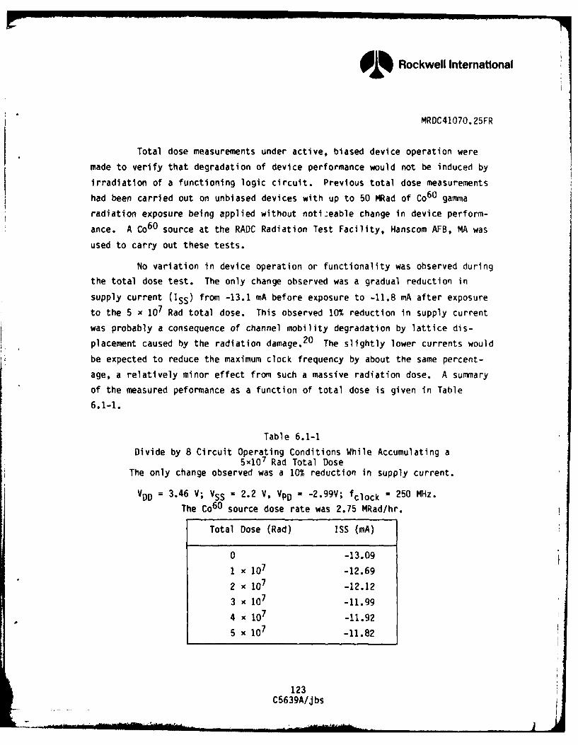
9 Rockwell International
MRDC41070.25FR
Total dose measurements under active, biased device operation were
made to verify that degradation of device performance would not be induced by
irradiation of a functioning logic circuit. Previous total dose measurements
had been carried out on unbiased devices with up to 50 MRad of Co60 gamma
radiation exposure being applied without noticeable change in device perform-
ance. A Co6 0 source at the RADC Radiation Test Facility, Hanscom AFB, MA was
used to carry out these tests.
No variation in device operation or functionality was observed during
the total dose test. The only change observed was a gradual reduction in
supply current (Iss) from -13.1 mA before exposure to -11.8 mA after exposure
to the 5 x 10⁷ Rad total dose. This observed 10% reduction in supply current
was probably a consequence of channel mobility degradation by lattice dis-
placement caused by the radiation damage. 20 The slightly lower currents would
be expected to reduce the maximum clock frequency by about the same percent-
age, a relatively minor effect from such a massive radiation dose. A summary
of the measured peformance as a function of total dose is given in Table6.1-1.
Table 6.1-1
Divide by 8 Circuit Operating Conditions While Accumulating a5x107 Rad Total Dose
The only change observed was a 10% reduction in supply current.
VDD = 3.46 V; VSS = 2.2 V, VpD = -2.99V; fclock = 250 MHz.
The Co6 0 source dose rate was 2.75 MRad/hr.
Total Dose (Rad) ISS (mA)
0 -13.09
1 x 10⁷ -12.69
2 x 10⁷ -12.12
3 x 10⁷ -11.99
4 x 10⁷ -11.92
5 x 10⁷ -11.82
123C5639A/J bs
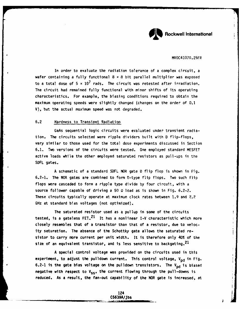
EjL Rockwell International
MRDC41070.25FR
In order to evaluate the radiation tolerance of a complex circuit, a
wafer containing a fully functional 8 x 8 bit parallel multiplier was exposed
to a total dose of 5 x 10⁷ rads. The circuit was retested after irradiation.
The circuit had remained fully functional with minor shifts of its operating
characteristics. For example, the biasing conditions required to obtain the
maximum operating speeds were slightly changed (changes on the order of 0.1
V), but the actual maximum speed was not degraded.
6.2 Hardness to Transient Radiation
GaAs sequential logic circuits were evaluated under transient radia-
tion. The circuits selected were ripple dividers built with D flip-flops,
very similar to those used for the total dose experiments discussed in Section
6.1. Two versions of the circuits were tested. One employed standard MESFET
active loads while the other employed saturated resistors as pull-ups in the
SDFL gates.
A schematic of a standard SDFL NOR gate D flip flop is shown in Fig.
6.2-1. The NOR gates are combined to form D-type flip flops. Two such flip
flops were cascaded to form a ripple type divide by four circuit, with a
source follower capable of driving a 50 Q load as is shown in Fig. 6.2-2.
These circuits typically operate at maximum clock rates between 1.9 and 2.2
GHz at standard bias voltages (not optimized).
The saturated resistor used as a pullup in some of the circuits
tested, is a gateless FET. 21 It has a nonlinear I-V characteristic which more
closely resembles that of a transistor than that of a resistor, due to veloc-
ity saturation. The absence of the Schottky gate allows the saturated re-
sistor to carry more current per unit width. It is therefore only 40% of the
size of an equivalent transistor, and is less sensitive to backgating.2 1
A special control voltage was provided on the circuits used in this
experiment, to adjust the pulldown current. This control voltage, Vpd in Fig.
6.2-1 is the gate bias voltage on the pulldown transistors. The Vpd is biased
negative with respect to Vss, the current flowing through the pull-downs is
reduced. As a result, the fan-out capability of the NOR gate is Increased, at
124C5639A/Jbs
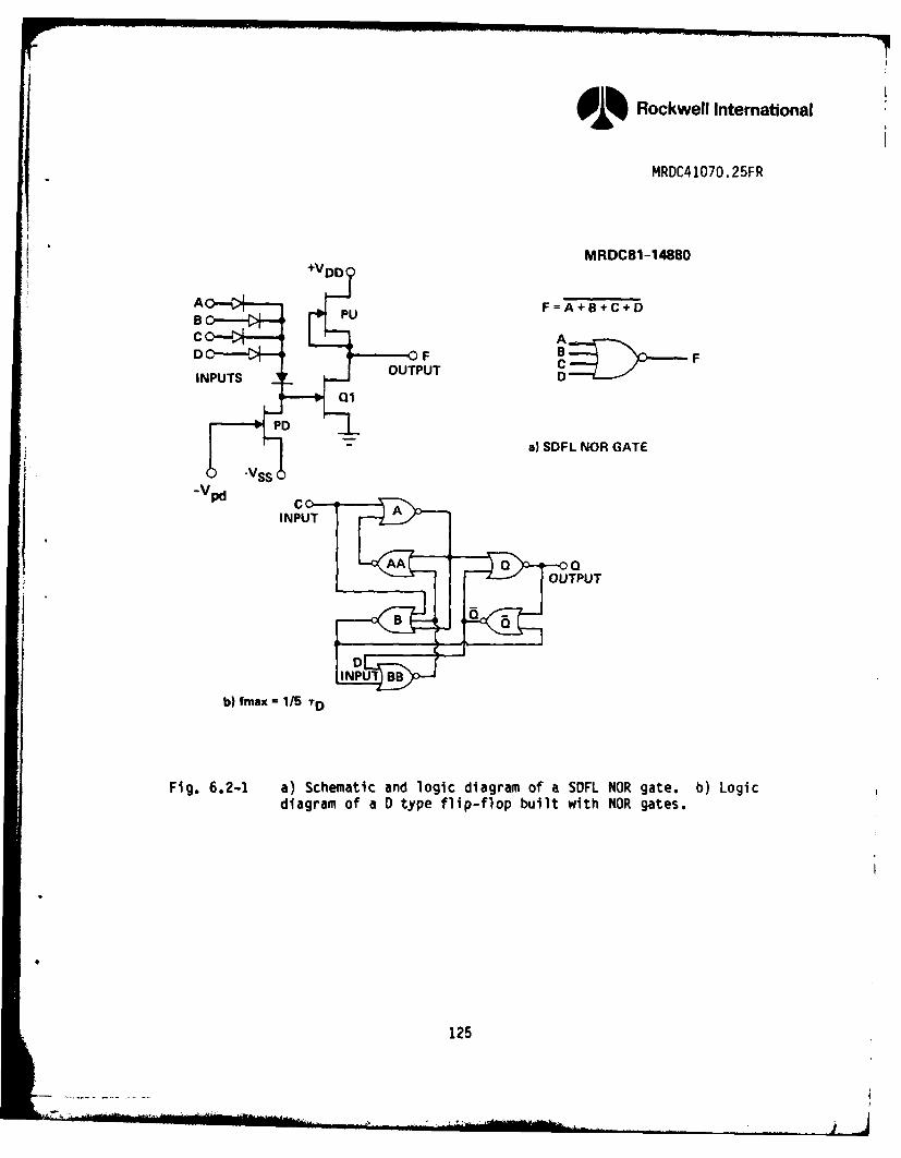
9Rockwell International
MRDC4 1070. 25FR
MRDC81-14880'+VDD
B PuC4 F=A+B+C+D
C AD F BFINPUTS OUPU
01
a) SDFL NOR GATE
V S-Vpd
INPUx 15 TD
F~~g.A 0.- a)Shmtcadlgcdarmo 0 DLNRgt.b oidiagam a tye flp-fop UTPwiTNRgts
125Q
A~Rockwell International
MRDC4 1070. 25FR
00
10. *4J
'-
LLL
'-L:
-j 4-
q r- 6)0
+ A.
1264
9 Rockwell International
MRDC41070.25FR
the expense of speed, because the lower pulldown current implies a slower dis-
charge of the switching FET's gate, when it goes from "on" to "off."
The experiments were performed at two locations; the Naval Research
Laboratory (NRL) in Washington, D.C., and the White Sands Missile Range in New
Mexico. A linear accelerator (LINAC), provided the electron beam used to ir-
radiate the circuits. The duration of the radiation pulses ranged between 20
ns and 60 ns. The dose rate was determined by the distance between the radia-
tion source and the device. Dose rates ranged between 1 x 10⁸ and
2 x 10¹⁰ rads/s. Measurement of the radiation dose of each pulse was made
using either a thermoluminescent device (TLD) or a silicon PIN diode.
The main effect that the radiation pulses had on the devices was to
increase the positive supply current, Idd, and to change the output level.
Both returned, following an exponential envelope, to the levels preceding the
pulse. The time required to return to within 10% of the initial value will
henceforth be referred to as the decay time. This is to be distinguished from
the recovery time, which is the time required for the circuit to resume proper
operation following an upset.
The long term transients were observed with a storage oscilloscope.
This allowed for the convenient evaluation of the decay times, which in some
instances were as long as 1 s. The output signal, in the immediate vicinity
of the radiation pulse, could not be clearly seen with this method. The short
term disturbances were observed using transient digitizers, where the output
signal could be clearly seen in the immediate vicinity of the radiation pulse,
but the sampling memory of the digitizers were insufficient for viewing longer
envelopes. Therefore, the data from the two experiments complemented each
other quite well. Samples of extended, and short time scale data are shown in
Figs. 6.2-3 and 6.2-4, respectively.
Figure 6.2-3 shows long term effects In a divide by four circuit, as
it is exposed to a pulse of 2 x 10¹⁰ rads/s. The upper oscillogram was taken
with the positive bias voltage Vdd a 2.5 V, and the lower oscillogram was
taken with Vdd = 3.0 V. There are two traces on each oscillogram. The upper
trace depicts the divide by four output, and the lower trace depicts the
127C5639A/Jbs
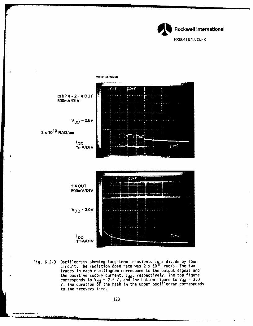
Q% Rockwell International
MRDC41070.25FR
MROC83-20750
CHIP4-.2+4OUT500mV/DIV
VDD = 2.5V
2 x10 1 0 RAD/sec
I lmA/DIV
500mV/D1V
VDD = 3 .OV
IDDlmA/DIV
Fig. 6.2-3 Oscillograms showing long-term transients i a divide by fourcircuit. The radiation dose rate was 2 x 10¹⁰ rad/s. The twotraces in each oscillogram correspond to the output signal andthe positive supply current, Idd, respectively. The top figurecorresponds to Vdd = 2.5 V, and the bottom figure to Vdd = 3.0V. The duration of the hash in the upper oscillogram correspondsto the recovery time.
128
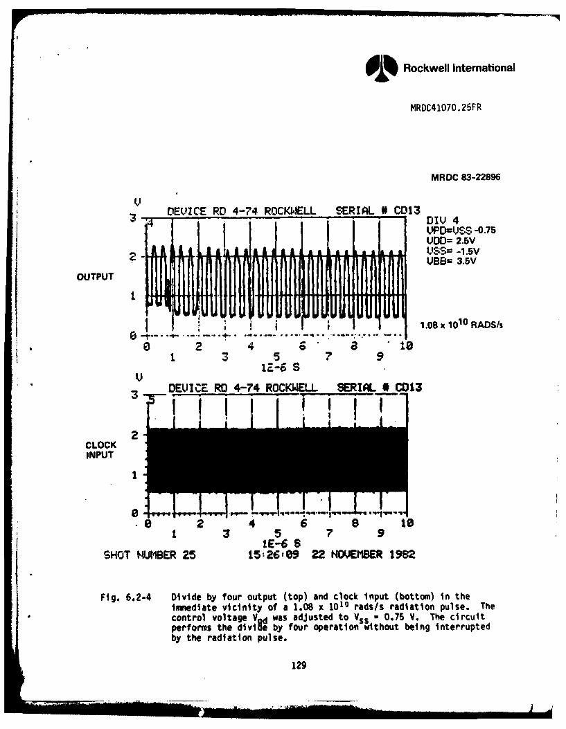
'Q Rockwell International
MRDC41070.25FR
MRDC 83-22896
VDEVICE RD 4-74 ROCK4ELL SERIAL # C013
- .DIV 4
VPD=USS -0.75UDD= 2.5V
2- U'S= -1.5VU86= 3,5V
OUTPUT
1.08 x 10¹⁰ RADS/s
0 2 4 a 185 7 9
1E-&S
VDEICE RD 4-74 ROCKWELL SERIAL M C013
2CLOCKINPUT
1
2 4 6 8l0 2 89g.i~.~'13 156 S 7 9
IE-6 SSHOT lU4BER 25 15:26,09 22 NOVEMBER 1982
Fig. 6.2-4 Divide by four output (top) and clock input (bottom) in theimmediate vicinity of a 1.08 x 10¹⁰ rads/s radiation pulse. Thecontrol voltage V d was adjusted to Vss " 0.75 V. The circuitperforms the diviSe by four operation without being interruptedby the radiation pulse.
129
94L Rockwell International
MRDC41070.25FR
positive supply current, Idd. Figure 6.2-4 shows a short term effect in
another divide by four circuit, as it was exposed to a pulse of 1 x 10¹⁰
rads/s. The upper waveform is the divide by four output, and the lower wave-
form is the clock input.
The observed devices showed various degrees of perturbations over the
range of dose rates evaluated. The consistent trends that were observed are
as follows: there is an expected increase in the amplitude of the positive
supply current, Idd, and the decay time increases as the dose rate increases.
Increasing the positive supply voltage, Vdd, decreases the decay time. This is
exemplified in Fig. 6.2-3. Although it is difficult to see exactly what is
happening to the output waveforms from the oscillograms, it can be easily in-
ferred that during the period where there is hash on the corresponding current
waveform, such as in the upper oscillogram of Fig. 6.2-3, and the circuit is
not dividing correctly. The hash represents changes in the supply current
corresponding to state changes of the counter. When the circuit divides cor-
rectly, this hash is not seen because the frequency of the current changes is
higher than the bandwidth of the amplifier used to monitor the current.
Therefore the hash indicates that the circuit is changing states less fre-
quently than that which is required for proper divide by four operation. The
duration of the hash then, is a reasonable representation of the recovery
time.
The 55 ms disturbance of the +4 output seen in the upper oscillogram
of Fig. 6.2-3 is reduced to a 1 ms period (barely detectable in the lower
oscillogram) when Vdd is increased. Other oscillograms taken under the same
experimental conditions, with shorter time sweeps, indicate that for most of
the 1 ms period, the output is dividing correctly, and the major disturbance
is a small shift in the output level that does not affect circuit functional-
ity. Another indication that the recovery time is extremely short in the
lower oscillogram is the fact that no hash Is detectable on the corresponding
current waveform. The time required for the circuit to resume the divide by
four operation is far shorter than the decay time.
130C5639A/Jbs
NONE&-
9 Rockwell International
MRDC41070.25FR
As Vpd is adjusted, and made increasingly more negative with respect
to Vss , the time for which the circuit is not dividing correctly is reduced to
the point where divide by four operation is not affected even at dose rates as
high as 1 x 10¹⁰ rads/s, as shown in Fig. 6.2-4. Here, Vpd was biased 0.75 V
below Vss. Under the same radiation conditions, with Vpd 0.3 V beneath Vssthe same device would sometimes miss a count, and not resume proper operation
until 3.5 ps after the radiation pulse. With Vpd 0.15 V beneath Vss, this
device did not divide properly for more than 10 us after the radiation pulse.
Thus we see that Vpd can be used to improve transient radiation hardness.
However, this is accomplished at the expense of maximum speed of operation.
This tradeoff was unnoticeable at the low frequencies (< 250 MHz) used for
these tests. Figure 6.2-5 shows data taken in a nonradiation environment,
showing how the maximum operating frequency of the devices decreases as Vpd is
biased negative with respect to Vss.
Circuits designed using saturated resistor pull-ups were observed to
be affected less than circuits with FET pullups. In several instances, cir-
cuits with FET loads would experience long term upsets, as shown in Fig. 6.2-
3, where the divide by four output would not be correct, and Idd would behave
erratically. A similar circuit with saturated resistor loads would experience
only a change in output level, and the Idd decay time would be shorter under
the same test conditions.
The results observed are consistent with those obtained in earlier
experiments.2 2 They indicate that pulsed ionizing radiation causes charge
trapping in the semi-insulating GaAs substrate.23 ,24 The higher the ionizing
radiation dose, the more charge trapping occurs. The result is an effect very
similar to that of backgating.23
The channels of the devices operating at the more positive potential
(the pullups) appear to be the most severely affected. Therefore, when Vdd is
increased, thereby increasing the current that the pullup devices can supply,
the circuits are less disturbed by transient radiation.
Since SOFL circuits have a wide voltage noise margin, the circuits
can still operate properly while the pull-up currents are altered. This
131C5639A/Jbs
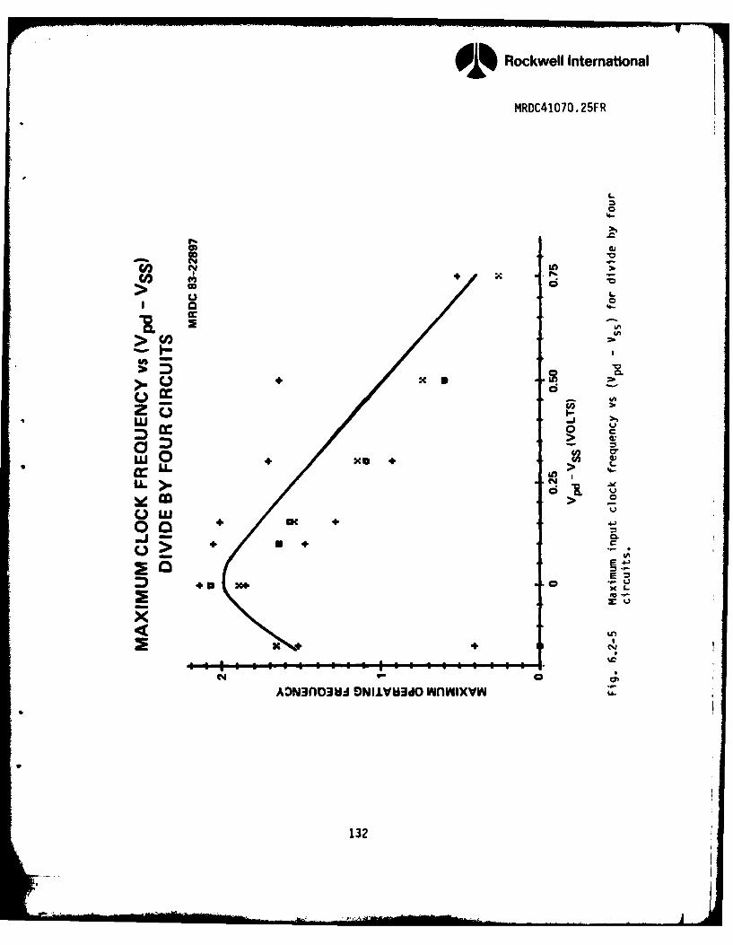
A)Rockwell International
MRDC41O7O 25FR
U))
d 4L
00
xu ia
LUO
000
L)
LUOnm DN1V'd wnU L
EL132
IMOWN-
Ei Rockwell International
MRDC41070.25FR
explains why the time required to resume proper logic operation (divide by
four) is observed to be much shorter than the decay time. On the other hand,
SDFL gates are sensitive to fanout because each gate is sinking current from
the previous stage. If the ratio between pull-up and pull-down currents is
reduced by radiation induced backgating, the circuit may fail to operate for
the time when the pullup can not provide enough current to the following
stages. Making Vpd more negative with respect to Vss raises the upset thres-
hold, and reduces the amount of pulldown current required (see Fig. 6.2-1).
This reduces the burden on the pullups, allowing them to supply sufficient
current to ensure proper logic levels. Note that the same effect obtained by
adjusting Vpd can be achieved by designing shorter width pulldown transistors.
Therefore, the additional control voltage, which is very convenient for exper-
imental purposes, does not need to be provided when a radiation hard circuit
is designed.
The saturated resistors were observed to be less affected by radia-
tion than were the equivalent FETs. This can be explained by the fact that
the saturated resistors channel is not initially depleted by the presence of a
Schottky gate. Therefore a smaller fraction of the channel depth is depleted
due to the charge trapped beneath the channel of the saturated resistor.
The experiments reported here confirm previous repors on the high
tolerance to transient radiation of GaAs integrated circuits. These, along
with high total dose hardness, are important assets for space applications of
this technology. From these experiments, a variety of bias voltage adjust-
ments, and design variations that can be used to control the divide by four
prescalers upset thresholds over dose rates ranging from 1 x 10⁸ to 2 x 10¹⁰
rads/s were determined. It was also shown how tradeoffs between speed and/or
power dissipation can be made to increase transient radiation hardness, over a
range of two orders of magnitude.
133C5639A/jbs
Rockwell International2
MRDC41O7O.25FR
7.0 MODELING OF MESFET DEVICES
The major thrust of this activity which was carried out at North
Carolina State University, was to develop accurate computer models for anal-
yzing the performance of short-channel GaAs MESFET devices as used in the
Rockwell VLSI circuits.
The modeling research was divided into three parts:
1. Two-dimensional finite difference simulation.
2. Two-dimensional Monte Carlo analysis.
3. Analytical modeling.
The intent was to use the two-dimensional analyses to give exact solutions to
the device operation and to serve as a guide for developing a simpler, and
less expensive, analytical model of sufficient accuracy to be valuable as a
design aid and to study effects of parameter changes.
In addition, work has been carried out in the characterization of
material and device properties using C-V and DLTS techniques.
In general, significant results have been obtained in all phases of
the program. The work on the two-dimensional model led to good predictions of
the major features of the ion implanted, 1 1iu gate MESFET. The Monte Carlo
analysis in general predicted currents almost three times higher than those
obtained from a conventional 20 device analysis program. This result suggest
that such conventional programs are inadequate for modelling of very small
devices due to their lack of consideration of velocity overshoot and other -
transient phenomena. An analytical model based on a two-piece approximation of
the velocity-field characteristics was proposed. This approximation is de-
fined from a theoretical velocity-field characteristic obtained by Monte Carlo
techniques. Finally, a measurement technique for determining free-carrier,
shallow-level donor, trap and mobility profiles of ion-implanted devices hasbeen successfully applied to a 1 wi gate length MESFET.
134C5639A/Jbs
Oil Rockwell International
MRDC41O7O. 25FR
A detailed description of the work here sunmarized can be found inAppendix B of this report.
I 35C5639A/Jbs
Oil% Rockwell International
* MRDC41O7 . 25FR
8.0 REFERENCES
1. R. Zucca et al., "Ion Implanted GaAs IC Process Technology," AnnualTechnical Report, Contract No. F49620-77-C-0087, July 1981.
2. J.L. Tandon, M-A. Nicolet and F.H. Eisen, Appi. Phys. Lett. Vol. 34,p. 2, 1979.
3. L.H. Skolnik, W.G. Spitzer, A. Kahan, F. Euler, and R.G. Hunsperger,J. Appi. Phys. Vol. 43, p. 2146, 1972.
4. H. Muller, F.H. Eisen, and J.W. Mayer, J. Electrochem. Soc. Vol. 122,p. 651, 1975.
5. M.G. Grimaldi, B.M. Paine, M-A. Nicolet, and D.K. Sadana, J. Appi.Phys., in press.
Sadana, Appl. Phys. Lett. Vol. 39, p. 70, 1981.
7. S.S. Kular, B.J. Sealy, K.G. Stephens, D. Sadana and G.R. Booker, Solid-State Electron. Vol. 23, p. 831, 1980.
8. J.S. Williams and M.W. Austin, Nucl. Instr. and Meth. Vol. 168, p. 307,1980.
9. J.S. Williams and M.W. Austin, Appl. Phys. Lett. Vol. 36, p. 994, 1980.
10. J.S. Williams, M.W. Austin and H.B. Harrison, in Thin Film Interfacesand Interactions, J.E.E. Baglin and J.M. Poate (e-d-s.,TheElectrochemicaT Society, Princeton, p. 187, 1980.
11. J.F. Gibbons, U.S. Johnson and S.W. Mylrole, Projected Range Statistics,Halstead, 1975.
12. Y. Kato, Y. Shiraki, T. Shimada, and K.F. Komatsurbara, J. Appl. Phys.Vol. 45, p. 1044 1974.
13. B.J. Sealy, J. Mat. Sdi. Vol. 10, p. 683, 1975.
14. N.H. Berger, "Contact Resistance and Contact Resistivity," J. Electro-chem. Soc. Vol. 119, No. 4, pp. 507-514, April 1972.
15. R. Zucca, B.M. Welch, R.C. Eden, and 5.1. Long, "GaAs Digital IC Tech-nology/Statistical Analysis of Device Performance," IEEE Trans. El.
* Dev., Vol. ED-27, No. 6, pp. 1109-1115, June 1980.
136C5639A/j bs
9D Rockwell International
MRDC41070.25FR
16. R. Vahrenkamp, R. Zucca and S.J. Lee, "Advanced On-Board Signal Proc-essor GaAs Memory," Final Technical Report, Contract No. MDA 903-81-C-0126, November 1983.
17. R.F. Van Tuyl, C.A. Leichti, R.E. Lee and E. Gowen, "GaAs MESFET Logicwith 4 GHz Clock Rate," IEEE J. Solid-State Circuits, SC-12, pp. 485-496, 1977.
18. R.C. Eden et al., "Multi-Level Logic Gate Implementation in GaAs ICsUsing Schottky Diode FET Logic," in 1980 ISSCC Tech. Digest, p. 122.
19. R. Zucca and R. Vahrenkamp, "Low-Power Radiation Hard RAM," Semi-AnnualTechnical Report No. 1, Contract No. MDA 903-3-C-0067, August 1983.
20. R. Zuleeg and K. Lehovec, "Radiation Effects in GaAs Junction FieldEffect Transistors," IEEE Trans. on Nucl. Sci., NS-27, No.5, pp. 1343-1354, Oct. 1980.
21. C.P. Lee, B.M. Welch, and R. Zucca, "Saturated Resistor Load for GaAsIntegrated Circuits," IEEE Transactions on Microwave Theory and Tech-niques, Vol. MTT-30 No. 7, pp. 1007-1013, July, 1982.
22. S. Long, F. Lee, and P. Pelligrini, "Pulsed Ionizing Radiation RecoveryCharacteristics of MSI GaAs Integrated Circuits," IEEE Electron DeviceLetters, Vol. EDL-2, pp. 173-176, July, 1981.
23. W.T. Anderson, M. Simmons, E.E. King, H.B. Dietrich and R.J. Lambert,"Long Term Transient Radiation Resistant GaAs FETs," IEEE ElectronDevice Letters, Vol. EDL-3, No. 9, pp. 248-250, September, 1982.
24. C.P., Lee and B.M. Welch, "GaAs MESFETs with Partial P-Type DrainRegions," IEEE Electron Device Letters, Vol. EDL-3, No. 7, pp. 200-202,July, 1982.
137C5639A/Jbs