Embed Size (px)
Citation preview

MicroBlaze Tutorial on EDK 10.1 using Spartan 3e
Ahmed Elhossini
January 24, 2010
1 Introduction
The Embedded Development Kit (EDK) from Xilinx allows the designer to build a complete processorsystem on Xilinx’s FPGAs. The systems that can be produced using EDK ranges from a simple singleprocessor architecture to a complex multi-processor system with multiple hardware accelerators. Thetool mainly supports two types of processors: i) MicroBlaze which is a reconfigurable soft-core processorand ii) Power-PC which is a hardcore processor implemented in some FPGAs from Xilinx. Dependingon the FPGA chip you are using, multiple Microblazes and Power-PCs can be integrated together in asingle design. EDK provides C/C++ compilers for both MicroBlaze and Power-PC along with severaltools for debugging/profiling of the applications running on each processor. Besides, using ISE, you canperform several types of simulations for the generated architectures which allows the estimation of boththe performance and power consumption of the architecture. This tutorial will demonstrate the processof creating and testing a MicroBlaze system design using the Embedded Development Kit (EDK) andSpartan 3e starter board from Xilinx.
1.1 Objectives
The tutorial contains these sections:
• System Requirements
• MicroBlaze System Description
• Tutorial Steps
The following steps are described in this tutorial:
• Starting XPS
• Using the Base System Builder Wizard
• Create or Import IP Peripheral
• Design Modification using Platform Studio
• Implementing the Design
• Defining the Software Design
• Downloading the Design
1

1.2 System Requirements
You must have the following software installed on your PC to complete this tutorial:
• Windows 2000 SP2/Windows XP
• EDK 10.1i.
• ISE 10.1i.
• Familiarity with Xilinx ISE 10.1 design flow.
• Spartan 3e starter kit and Xilinx USB download cable.
Note: It should be noted that other hardware could be used with this tutorial. However, thecompleted design has only been verified on the board specified above. The following designchanges are required if using a different platform:
• Update pin assignments in the system.ucf file
• Update board JTAG chain specified in the download.cmd
1.3 MicroBlaze System Description
In general, to design an embedded processor system, you need the following:
• Hardware components
• Memory map
• Software application
1.3.1 Tutorial Design Hardware
The MicroBlaze (MB) tutorial design includes the following hardware components:
• MicroBlaze
• Local Memory Bus (LMB) Bus
• LMB BRAM IF CNTLR
• BRAM BLOCK
• PLB Bus
• Multi-Port Memory Controller (MPMC)
• MDM
• XPS UARTLITE
• 2 - XPS GPIOs
1.3.2 Tutorial Design Memory Map
The following table shows the memory map for the tutorial design as created by Base System Builder.
2

AddressDevice Min Max Size Comment
LMB BRAM 0x0000 0000 0x0000 3FFF 16K bytes LMB MemoryMDM 0x8440 0000 0x8440 FFFF 64K bytes debug module
XPS UARTLITE 0x8400 0000 0x8400 FFFF 64K bytes RS232 DCEXPS GPIO 0x8140 0000 0x8140 FFFF 64K bytes LEDs 8BitXPS GPIO 0x8142 0000 0x8142 FFFF 64K bytes DIP Switches 4Bit
MPMC 0x8600 0000 0x87FF FFFF 32M bytes DDR SDRAM
Table 1: Table 1: Tutorial Design Memory Map
1.4 Tutorial Steps
1.4.1 Setup
Spartan 3e starter board with a RS-232 terminal connected to the serial port and configured for 57600baud, with 8 data bits, no parity and no handshakes.
1.4.2 Creating the Project File in XPS
The first step in this tutorial is using the Xilinx Platform Studio (XPS) to create a project file. XPSallows you to control the hardware and software development of the MicroBlaze system, and includes thefollowing:
• An editor and a project management interface for creating and editing source code
• Software tool flow configuration options
You can use XPS to create the following files:
(i) A Project Navigator project file that allows you to control the hardware implementation flow
(ii) A Microprocessor Hardware Specification (MHS) file
Note: For more information on the MHS file, refer to the “Microprocessor HardwareSpecification (MHS)” chapter in the Platform Specification Format Reference Manual.
(iii) Microprocessor Software Specification (MSS) file
Note: For more information on the MSS file, refer to the “Microprocessor SoftwareSpecification (MSS)” chapter in the Platform Specification Format Reference Manual.
XPS supports the software tool flow associated with these software specifications. Additionally, you canuse XPS to customize software libraries, drivers, and interrupt handlers, and to compile your programs.
2 Starting XPS
(i) To open XPS, select Start→ All Programs→ Development→ Xilinx ISE Design Suite 10.1→ EDK→ Xilinx Platform Studio
3

(ii) Select Base System Builder Wizard (BSB) to open the “Create New XPS Project Using BSBWizard” dialogue box shown in Figure 1.
(iii) Click Ok.
(iv) Use the Project File Browse button to browse to the folder you want as your project directory.
(v) Click Open to create the system.xmp file then Save.
(vi) Click Ok to start the BSB wizard. The wizard window will appear, which will be used to build thedesign as will be discussed in following sections.
Note: XPS does not support directory or project names which include spaces.
Figure 1: Create New XPS Project Using Base System Builder Wizard
3 Defining the System Hardware
3.1 MHS and MPD Files
The next step in the tutorial is defining the embedded system hardware with the Microprocessor HardwareSpecification (MHS) and Microprocessor Peripheral Description (MPD) files.
3.1.1 MHS File
The Microprocessor Hardware Specification (MHS) file describes the following:
• Embedded processor: either the soft core MicroBlaze processor or the hard core PowerPC (onlyavailable in Virtex-II Pro and Virtex-4 FX devices)
• Peripherals and associated address spaces
• Buses
• Overall connectivity of the system
The MHS file is a readable text file that is an input to the Platform Generator (the hardware systembuilding tool). Conceptually, the MHS file is a textual schematic of the embedded system. To instantiatea component in the MHS file, you must include information specific to the component.
4

3.1.2 MPD File
Each system peripheral has a corresponding MPD file. The MPD file is the symbol of the embedded sys-tem peripheral to the MHS schematic of the embedded system. The MPD file contains all of the availableports and hardware parameters for a peripheral. The tutorial MPD file is located in the following directory:
$XILINX EDK/hw/XilinxProcessorIPLib/pcores/ < peripheral name > /data
Note: For more information on the MPD and MHS files, refer to the “Microprocessor Pe-ripheral Description (MPD)” and “Microprocessor Hardware Specification (MHS)” chaptersin the Embedded System Tools Guide.
EDK provides two methods for creating the MHS file. Base System Builder Wizard and the Add/EditCores Dialog assist you in building the processor system, which is defined in the MHS file. This tutorialillustrates the Base System Builder.
4 Using the Base System Builder Wizard
Use the following steps to create the processor system:
• In the Base System Builder - Select “I would like to create a new design” then click Next.
• In the Base System Builder - Select Board Dialog select the following, as shown in Figure 2:
– Board Vendor: Xilinx
– Board Name: Spartan-3E Starter Board
– Board Revision: C
• Click Next. Select the MicroBlaze
• Click Next. You will now specify several processor options as shown in Figure 3:
The following is an explanation of the settings specified in Figure 3:
• System Wide Setting:
– Reference clock frequency: This is the on board frequency of the clock.
– Processor-Bus clock frequency: This is the frequency of the clock driving the processor system.
• Processor Configuration:
– Debug I/F:
∗ On-Chip H/W Debug module: When the H/W debug module is selected; a PLB MDMmodule is included in the hardware system. This introduces hardware intrusive debuggingwith no software stub required. This is the recommended way of debugging for MicroBlazesystem.∗ XMD with S/W Debug stub: Selecting this mode of debugging interface introduces a soft-
ware intrusive debugging. There is a 1200-byte stub that is located at 0x00000000. Thisstub communicates with the debugger on the host through the JTAG interface of the PLBMDM module.
5

Figure 2: BSB: Select a Board
6

Figure 3: Configure Processor
7

∗ No Debug: debugging is disabled.
Note: For more information about the Xilinx Microprocessor Debugger (XMD),refer to the Xilinx Microprocessor Debugger (XMD) chapter in the EmbeddedSystem Tools Reference Manual.
– Users can specify the size of the local instruction and data memory.
– Cache setup:
∗ No Cache: No caching will be used∗ Enable cache link: Caching will be used through the FSL bus
– You can also specify the use of the floating point unit (FPU).
– Click Next.
Select the peripheral subset (Configure IO Interfaces wizard) as shown in Figure 4, Figure 5 and Figure 6.It should be noted that the number of peripheral shown on each dialogue box is dynamic based upon yourcomputers resolution.
In the first page of the “Configure IO Interfaces wizard”, Figure 4:
• RS232 DTE → deselect
• RS232 DCE → select
• XPS UARTLITE baud-rate → 57600, data bits → 8 and Parity → NONE
• LEDs 8Bit → select
• Click Next
In the second page of the “Configure IO Interfaces wizard”, Figure 5:
• DIP Switch 4Bit → select
• Buttons 4Bit → deselect
• FLASH → deselect
• SPI FLASH → deselect
• Click Next
In the third page of the “Configure IO Interfaces wizard”, Figure 6:
• DDR SDRAM → select
• Ethernet Mac → deselect
• Click Next through the Add Internal Peripherals page as we will not add any in this tutorial.
• Click Next
This completes the hardware specification and we will now configure the software settings. Using theSoftware Setup dialogue box as shown in Figure 7, specify the following software settings:
8

Figure 4: Configure I/O Interfaces - 1
9

Figure 5: Configure I/O Interfaces - 2
10

Figure 6: Configure I/O Interfaces - 3
11

• Standard Input (STDIN) → RS232
• Standard Output (STDOUT) → RS232
• Boot Memory → ilmb cntlr
• Sample Application Selection → Memory Test
• Click Next.
Using the Configure Memory Test Application dialogue box as shown in Figure 8, specify the followingsoftware settings:
• Instructions → ilmb cntlr
• Data → dlmb cntlr
• Stack/Heap → dlmb cntlr
• Click Next.
The completed system including the memory map will be displayed as shown in Figure 9. Currently thememory map cannot be changed or updated in the BSB. If you want to change the memory map you cando this in XPS.
• Click Generate and then Finish, to complete the design.
• Select “Start Using Platform Studio” and click OK.
4.1 Review
The Base System Builder Wizard has created the hardware and software specification files that define theprocessor system. When we look at the project directory, shown in Figure 10, we see these as system.mhsand system.mss. There are also some directories created:
• data - contains the UCF (user constraints file) for the target board.
• etc - contains system settings for JTAG configuration on the board that is used when downloadingthe bit file and the default parameters that are passed to the ISE tools.
• pcores - is empty right now, but is utilized for custom peripherals.
• TestApp Memory - contains a user application in C code source, for testing the memory in the system.
4.2 Project Options
To see the project options that Base System Builder has configured select: Project→ Project Options. Asshown in Figure 11, the device information is specified.
Select: Hierarchy and Flow. This window is shown in Figure 12. This window provides the opportunityto export the processor system into an ISE project as either the top level system or a sub-module design.
12

Figure 7: Software Setup
13

Figure 8: Configure Memory Test Application
14

Figure 9: Completed Processor System
Figure 10: Project Directory
15

Figure 11: Project Options - Device and Repository
Figure 12: Project Options - Hierarchy and Flow
16

Figure 13: Create Peripheral - Name and Version
5 Create or Import IP Peripheral
One of the key advantages of building an embedded system in an FPGA is the ability to include customIP that interface to the processor. This section of the tutorial will walk through the steps necessary toinclude a custom IP core.
• In XPS, select Hardware→ Create or Import Peripheral . . . to open the Create and Import PeripheralWizard.
• Click Next. Select Create templates for a new peripheral.
By default the new peripheral will be stored in the project directory/pcores directory. This enables XPSto find the core for utilization during the embedded system development.
• Click Next. In the Create Peripheral - Name and Version dialogue, enter “custom ip” as the nameof the peripheral. This is shown in Figure 13.
• Click Next. In the Create Peripheral - Bus Interface dialogue. Select Processor Local Bus(PLBv4.6), as this is the bus to which the new peripheral will be connected.
• Click Next. The Create Peripheral - IPIF Services dialogue enables the selection of several services.For additional information regarding each of these services, select More Info. Select the User logicS/W register support option as shown in Figure 14.
• Click Next. In Slave interface, do not change anything
17

Figure 14: Create Peripheral - IPIF Services
• Click Next. In the Create Peripheral - User S/W Register dialogue, change the Number of softwareaccessible registers to 4 as shown in Figure 15.
• Click Next. In the Create Peripheral - IP Interconnect (IPIC).
• Click Next. In the Create Peripheral - (OPTIONAL) Peripheral Simulation Support dialogue, aBus Functional Model (BFM) simulation environment can be generated. This tutorial will not coverBFM simulation. Leave the option unchecked.
• Click Next. In the Create Peripheral - (OPTIONAL) Peripheral Implementation Support dialogue,uncheck the Generate ISE and XST project files to help you implement the peripheral using XSTflow.
• Click Next.
• Click Finish.
The Create or Import Peripheral Wizard creates a new directory called custom ip v1 00 a in the pcoresdirectory. This new directory contains hdl source directory, drivers directory and data directory as seenin Figure 16.In the hdl directory several source files cab be identified:
• mb tut 1\pcores\custom ip v1 00 a\hdl
– custom ip.vhdThis is the template file for your peripheral’s top design entity. It configures and instantiates
18

Figure 15: Create Peripheral - User S/W Register
Figure 16: Custom IP Directory Structure
19

the corresponding IPIF unit in the way you indicated in the wizard GUI and connect it to thestub user logic where the user logic should get implemented. You are not expected to modifythis template file except in certain marked places for adding user specific generics and ports.
– user logic.vhdThis is the template file for the stub user logic design entity, either in VHDL or Verilog, wherethe actual functionalities should get implemented. Some sample code may be provided fordemonstration purpose.
– XPS interface file(s)
In the data directory several source files cab be identified:
• mb tut 1\pcores\custom ip v1 00 a\data
– custom ip v2 1 0.mpd This Microprocessor Peripheral Description file contains interface in-formation of your peripheral so that other EDK tools can recognize the peripheral.
– custom ip v2 1 0.pao This Peripheral Analysis Order file defines the analysis order of all theHDL source files that are used to compile your peripheral.
In the Drivers directory several source files can be identified:
• mb tut 1\drivers\custom ip v1 00 a\src :
– custom ip.h This is the software driver header template file, which contains address offsets ofsoftware addressable registers in your peripheral, as well as some common masks, simple registeraccess macros and function declarations.
– custom ip.c This is the software driver source template file to define all applicable driverfunctions.
– custom ip selftest.c This is the software driver self test example file which contain self testexample code to test various hardware features of your peripheral.
– makefile This is the software driver makefile to compile drivers.
Now that the template has been created, the user logic.vhd file could be modified to incorporate thecustom IP functionality.
• Open user logic.vhd. Currently the code provides an example of reading and writing to four 32-bitregisters. For the purpose of this tutorial, this code will not be modified.
• Close user logic.vhd
In order for XPS to add the new custom IP core to the design, the pcores directory must be res-canned. This can be accomplished by selecting Project → Rescan User Repositories. XPS alsoautomatically rescans the pcores directory when the project is opened.
6 Design Modification using Platform Studio
Once a design has been created with the Base System Builder, it can be modified from within the SystemAssembly view.
Double clicking on any of the IP’s listed in the System Assembly View allows modification of that particularIP as shown in Figure 17. The System Assembly View has the following tabs:
20

Figure 17: System Assembly View
Bus Interfaces: With the Bus Interface activated, the patch panel to the left of the System AssemblyView gets activated. The bus connectivity of the core is shown when the hierarchy of the IP isexpanded.
Ports: With this filter on, the port connections appear when the hierarchy of the IP is expanded. Youneed to activate this filter to be able to add external ports.
Addresses: The IP’s addresses can be viewed when expanding the IP. This is where you can generateaddresses for the IP’s.
On the left hand side of XPS, the user can choose from three views, Project, Applications and IPCatalog. The IP Catalog tab shows all of the IP that is available to use in the EDK project. To add newIP:
• Bring the IP Catalog tab forward.
• Expand the Project Repository hierarchy.
• Select CUSTOME IP.
• Drag and drop the IP into the System Assembly View or double click on the IP.
• The new IP custome ip 0 should appear in the assembly view as shown in Figure 18.
With the Bus Interfaces tab brought forward (Figure 19):
• Press the Connection Filter button and select All
• Expand the custom ip 0 instance
21

Figure 18: Inserting IP
• High-light the slave PLB connection (SPLB)
• Select the No Connection pull down menu and change it to mb plb
Note: Right clicking on the Name column in the System Assembly View provides more fil-tering options.
Select the Addresses tab to define an address for the newly added custom ip peripheral. The address canbe assigned by entering the Base Address or the tool can assign an address. For the purpose of this tutorial,the tool will be used to assign an address.
• Change the size of the dlmb cntlr and ilmb cntlr to 16K.
• Click Generate Addresses.
A message in the console window will state that the address map has been generated successfully. Thedesign is now ready to be implemented.
7 Implementing the Design
Now that the hardware has been completely specified in the MHS file, you can run the Platform Generator.Platform Generator elaborates the MHS file into a hardware system consisting of NGC files that representthe processor system. Then the Xilinx ISE tools will be called to implement the design for the targetboard. To generate a netlist and create the bit file, follow these steps:
22

Figure 19: Modifying bus connections
Figure 20: Software Platform Settings Dialog
• Select Hardware→ Generate Netlist. This will elaborate the MHS file and generate a netlist for thecomplete system (this will take a while!).
• Select Hardware → Generate Bitstream. This will call ISE tools to implement the design andgenerate a bit file that could be downloaded into the FPGA.
At the end of this step the XPS output screen should look like Figure 20. The bit file that is generate iscalled system.bit which contains all the required information to configure the FPGA except the contentsof the block ram (application/data). The bit file will be updated with the application code after definingthe software design.
8 Defining the Software Design
Now that the hardware design is completed, the next step is defining the software design. There are twomajor parts to software design, configuring the Board Support Package (BSP) and writing the softwareapplications. The configuration of the BSP includes the selection of device drivers and libraries.
23

Figure 21: Software Platform Settings Dialog
8.1 Configuration of the BSP
Configuration of the BSP is done using the Software Platform Settings dialogue. Inside of ISE, doubleclick on the EDK project file to open up XPS. In XPS, select Software → Software Platform Settings . . .This will open the Software Platform Settings dialogue box as shown in Figure 21. The Software PlatformSettings dialogue box contains three views. Each view is used to control all aspects of the BSP creation.
• The Software Platform view allows the user to modify processor parameters, driver, operating systemand libraries. The following Operating Systems are supported:
– Standalone
– xilkernel
– uclinux
– nucleus
No changes are required in this view.
• Select the OS and Libraries view as shown in Figure 22. This view allows the user to configure OSand library parameters.
No changes are required.
24

Figure 22: OS and Libraries view
Figure 23: Drivers view
• Select the Drivers view. This view allows you to select the software versions for the peripherals inthe system as shown in Figure 23. Notice that the driver version is independent of the HW version.
The Interrupt Handlers view allows you to modify the parameters for the interrupts. This project doesnot have any interrupts.
• Click OK.
• In XPS, select Software → Generate Libraries and BSPs to run LibGen and create the BSP whichincludes device drivers, libraries, configures the STDIN/STDOUT, and Interrupt handlers associatedwith the design.
LibGen creates the following directories in the microblaze 0 directory, shown in Figure 24:
• code: contains the compiled and linked application code in an ELF file
• include: contains the header files for peripherals included in the design (such as xgpio.h and xuar-tlite.h)
• lib: contains the library files (such as libc.a and libxil.a)
• libsrc: contains the source files used to create libraries
Note: For more information on these files, refer to the Embedded System Tools Guide.
25

Figure 24: MicroBlaze Drivers Directories
8.2 Building the User Application
In EDK 10.1, XPS provides for the user with the ability to create multiple software projects. These projectscan include source files, header files, and linker scripts. Unique software projects allow the designer tospecify the following options for each software project:
• Specify compiler options
• Specify which projects to compile
• Specify which projects to download
• Build entire projects
Software application code development can be managed by selecting the Applications tab as shown inFigure 25. The Base System Builder (BSB) generates a sample application which tests a subset of theperipherals included in the design.
8.3 Compiling the Code
Using the GNU GCC Compiler, compile the application code as follows:
• Select Software → Build All User Applications to run mb-gcc. Mb-gcc compiles the source files asshown in Figure 26.
Note: The software flow is independent of hardware implementation. Every time a changeis made to the software part of the system, there will be no need to build the hardware. Justupdate the bitstream file with the new application.
9 Downloading the Design
Now that the hardware and software designs are completed, the device can be configured. Follow thesesteps to download and configure the FPGA:
• Connect the host computer to the target board, including connecting the Xilinx USB download cableand the serial cable.
• Start a hyperterminal session with the following settings:
– com1 . This is dependant on the com port your serial cable is connected to.
– Bits per second: 57600
26
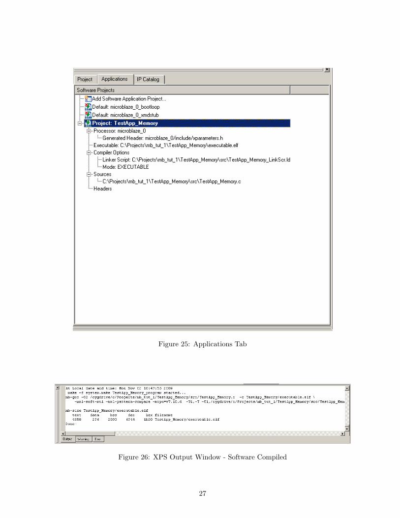
Figure 25: Applications Tab
Figure 26: XPS Output Window - Software Compiled
27

Figure 27: Hyperterminal Output
– Data bits: 8
– Parity: none
– Stop bits: 1
– Flow control: none
• Connect the board power
• In EDK, select Device Configuration → Update Bitstream. This will update the bit file with theapplication compiled code. Repeat this step each time the application changes.
• Select Device Configuration → Download Bitstream. This will start device configuration software(iMPACT) within EDK and executes the download command file etc/download.cmd.
• iMPACT will download the file download.bit on the FPGA.
Note: In some cases iMPACT fails to recognize the cable automatically. In this case etc/-download.cmd needs to be modified to manually select the cable. Modify the line setCable-p Auto to point to the correct cable; usb21 for exampleAfter the configuration is complete, you should see a display similar to that in shown in Figure 27:
28