Embed Size (px)
Citation preview

R
MicroBlazeProcessorReference GuideEmbedded Development KitEDK 6.3i
UG081 (v4.0) August 24, 2004

MicroBlaze Processor Reference Guide www.xilinx.com UG081 (v4.0) August 24, 20041-800-255-7778

UG081 (v4.0) August 24, 2004 www.xilinx.com MicroBlaze Processor Reference Guide1-800-255-7778
"Xilinx" and the Xilinx logo shown above are registered trademarks of Xilinx, Inc. Any rights not expressly granted herein are reserved.
CoolRunner, RocketChips, Rocket IP, Spartan, StateBENCH, StateCAD, Virtex, XACT, XC2064, XC3090, XC4005, and XC5210 areregistered trademarks of Xilinx, Inc.
The shadow X shown above is a trademark of Xilinx, Inc.
ACE Controller, ACE Flash, A.K.A. Speed, Alliance Series, AllianceCORE, Bencher, ChipScope, Configurable Logic Cell, CORE Generator,CoreLINX, Dual Block, EZTag, Fast CLK, Fast CONNECT, Fast FLASH, FastMap, Fast Zero Power, Foundation, Gigabit Speeds...andBeyond!, HardWire, HDL Bencher, IRL, J Drive, JBits, LCA, LogiBLOX, Logic Cell, LogiCORE, LogicProfessor, MicroBlaze, MicroVia,MultiLINX, NanoBlaze, PicoBlaze, PLUSASM, PowerGuide, PowerMaze, QPro, Real-PCI, RocketIO, SelectIO, SelectRAM, SelectRAM+,Silicon Xpresso, Smartguide, Smart-IP, SmartSearch, SMARTswitch, System ACE, Testbench In A Minute, TrueMap, UIM, VectorMaze,VersaBlock, VersaRing, Virtex-II Pro, Virtex-II EasyPath, Wave Table, WebFITTER, WebPACK, WebPOWERED, XABEL, XACT-Floorplanner, XACT-Performance, XACTstep Advanced, XACTstep Foundry, XAM, XAPP, X-BLOX +, XC designated products, XChecker,XDM, XEPLD, Xilinx Foundation Series, Xilinx XDTV, Xinfo, XSI, XtremeDSP and ZERO+ are trademarks of Xilinx, Inc.
The Programmable Logic Company is a service mark of Xilinx, Inc.
All other trademarks are the property of their respective owners.
Xilinx, Inc. does not assume any liability arising out of the application or use of any product described or shown herein; nor does it conveyany license under its patents, copyrights, or maskwork rights or any rights of others. Xilinx, Inc. reserves the right to make changes, at anytime, in order to improve reliability, function or design and to supply the best product possible. Xilinx, Inc. will not assume responsibility forthe use of any circuitry described herein other than circuitry entirely embodied in its products. Xilinx provides any design, code, orinformation shown or described herein "as is." By providing the design, code, or information as one possible implementation of a feature,application, or standard, Xilinx makes no representation that such implementation is free from any claims of infringement. You areresponsible for obtaining any rights you may require for your implementation. Xilinx expressly disclaims any warranty whatsoever withrespect to the adequacy of any such implementation, including but not limited to any warranties or representations that the implementationis free from claims of infringement, as well as any implied warranties of merchantability or fitness for a particular purpose. Xilinx, Inc. devicesand products are protected under U.S. Patents. Other U.S. and foreign patents pending. Xilinx, Inc. does not represent that devices shownor products described herein are free from patent infringement or from any other third party right. Xilinx, Inc. assumes no obligation tocorrect any errors contained herein or to advise any user of this text of any correction if such be made. Xilinx, Inc. will not assume anyliability for the accuracy or correctness of any engineering or software support or assistance provided to a user.
Xilinx products are not intended for use in life support appliances, devices, or systems. Use of a Xilinx product in such applications withoutthe written consent of the appropriate Xilinx officer is prohibited.
The contents of this manual are owned and copyrighted by Xilinx. Copyright 1994-2004 Xilinx, Inc. All Rights Reserved. Except as statedherein, none of the material may be copied, reproduced, distributed, republished, downloaded, displayed, posted, or transmitted in any formor by any means including, but not limited to, electronic, mechanical, photocopying, recording, or otherwise, without the prior written consentof Xilinx. Any unauthorized use of any material contained in this manual may violate copyright laws, trademark laws, the laws of privacy andpublicity, and communications regulations and statutes.
R

MicroBlaze Processor Reference Guide www.xilinx.com UG081 (v4.0) August 24, 20041-800-255-7778
MicroBlaze Processor Reference GuideUG081 (v4.0) August 24, 2004
The following table shows the revision history for this document.
Version Revision
10/01/02 1.0 Xilinx EDK 3.1 release
03/11/03 2.0 Xilinx EDK 3.2 release
09/24/03 3.0 Xilinx EDK 6.1 release
02/20/04 3.1 Xilinx EDK 6.2 release
08/24/04 4.0 Xilinx EDK 6.3 release

MicroBlaze Processor Reference Guide www.xilinx.com 5UG081 (v4.0) Augusti 24, 2004 1-800-255-7778
Preface: About This GuideManual Contents . . . . . . . . . . . . . . . . . . . . . . . . . . . . . . . . . . . . . . . . . . . . . . . . . . . . . . . . . . . . . 7Additional Resources . . . . . . . . . . . . . . . . . . . . . . . . . . . . . . . . . . . . . . . . . . . . . . . . . . . . . . . . 7Conventions . . . . . . . . . . . . . . . . . . . . . . . . . . . . . . . . . . . . . . . . . . . . . . . . . . . . . . . . . . . . . . . . . 8
Typographical . . . . . . . . . . . . . . . . . . . . . . . . . . . . . . . . . . . . . . . . . . . . . . . . . . . . . . . . . . . . . 8Online Document . . . . . . . . . . . . . . . . . . . . . . . . . . . . . . . . . . . . . . . . . . . . . . . . . . . . . . . . . . 9
Chapter 1: MicroBlaze ArchitectureOverview . . . . . . . . . . . . . . . . . . . . . . . . . . . . . . . . . . . . . . . . . . . . . . . . . . . . . . . . . . . . . . . . . . . 11
Features . . . . . . . . . . . . . . . . . . . . . . . . . . . . . . . . . . . . . . . . . . . . . . . . . . . . . . . . . . . . . . . . . 11Data Types and Endianness . . . . . . . . . . . . . . . . . . . . . . . . . . . . . . . . . . . . . . . . . . . . . . . . . 12Instructions . . . . . . . . . . . . . . . . . . . . . . . . . . . . . . . . . . . . . . . . . . . . . . . . . . . . . . . . . . . . . . . . . 13Registers . . . . . . . . . . . . . . . . . . . . . . . . . . . . . . . . . . . . . . . . . . . . . . . . . . . . . . . . . . . . . . . . . . . . 18
General Purpose Registers . . . . . . . . . . . . . . . . . . . . . . . . . . . . . . . . . . . . . . . . . . . . . . . . . 18Special Purpose Registers . . . . . . . . . . . . . . . . . . . . . . . . . . . . . . . . . . . . . . . . . . . . . . . . . . 19
Pipeline . . . . . . . . . . . . . . . . . . . . . . . . . . . . . . . . . . . . . . . . . . . . . . . . . . . . . . . . . . . . . . . . . . . . . 23Pipeline Architecture . . . . . . . . . . . . . . . . . . . . . . . . . . . . . . . . . . . . . . . . . . . . . . . . . . . . . . 23Branches. . . . . . . . . . . . . . . . . . . . . . . . . . . . . . . . . . . . . . . . . . . . . . . . . . . . . . . . . . . . . . . . . 24
Memory Architecture. . . . . . . . . . . . . . . . . . . . . . . . . . . . . . . . . . . . . . . . . . . . . . . . . . . . . . . . 24Reset, Interrupts, Exceptions and Break. . . . . . . . . . . . . . . . . . . . . . . . . . . . . . . . . . . . . . 25
Reset . . . . . . . . . . . . . . . . . . . . . . . . . . . . . . . . . . . . . . . . . . . . . . . . . . . . . . . . . . . . . . . . . . . . 25Interrupt . . . . . . . . . . . . . . . . . . . . . . . . . . . . . . . . . . . . . . . . . . . . . . . . . . . . . . . . . . . . . . . . 26User Vector (Exception) . . . . . . . . . . . . . . . . . . . . . . . . . . . . . . . . . . . . . . . . . . . . . . . . . . . 26Hardware Exceptions . . . . . . . . . . . . . . . . . . . . . . . . . . . . . . . . . . . . . . . . . . . . . . . . . . . . . 27Breaks . . . . . . . . . . . . . . . . . . . . . . . . . . . . . . . . . . . . . . . . . . . . . . . . . . . . . . . . . . . . . . . . . . . 27
Instruction Cache . . . . . . . . . . . . . . . . . . . . . . . . . . . . . . . . . . . . . . . . . . . . . . . . . . . . . . . . . . . 28Overview . . . . . . . . . . . . . . . . . . . . . . . . . . . . . . . . . . . . . . . . . . . . . . . . . . . . . . . . . . . . . . . . 28Instruction Cache Organization . . . . . . . . . . . . . . . . . . . . . . . . . . . . . . . . . . . . . . . . . . . . . 28General Instruction Cache Functionality . . . . . . . . . . . . . . . . . . . . . . . . . . . . . . . . . . . . . 28Instruction Cache Operation . . . . . . . . . . . . . . . . . . . . . . . . . . . . . . . . . . . . . . . . . . . . . . . 29Instruction Cache Software Support . . . . . . . . . . . . . . . . . . . . . . . . . . . . . . . . . . . . . . . . . 30
Data Cache . . . . . . . . . . . . . . . . . . . . . . . . . . . . . . . . . . . . . . . . . . . . . . . . . . . . . . . . . . . . . . . . . . 31Overview . . . . . . . . . . . . . . . . . . . . . . . . . . . . . . . . . . . . . . . . . . . . . . . . . . . . . . . . . . . . . . . . 31Data Cache Organization . . . . . . . . . . . . . . . . . . . . . . . . . . . . . . . . . . . . . . . . . . . . . . . . . . 31General Data Cache Functionality . . . . . . . . . . . . . . . . . . . . . . . . . . . . . . . . . . . . . . . . . . . 31Data Cache Operation . . . . . . . . . . . . . . . . . . . . . . . . . . . . . . . . . . . . . . . . . . . . . . . . . . . . . 32Data Cache Software Support . . . . . . . . . . . . . . . . . . . . . . . . . . . . . . . . . . . . . . . . . . . . . . 33
Fast Simplex Link (FSL) . . . . . . . . . . . . . . . . . . . . . . . . . . . . . . . . . . . . . . . . . . . . . . . . . . . . . 34Hardware Acceleration using FSL. . . . . . . . . . . . . . . . . . . . . . . . . . . . . . . . . . . . . . . . . . . 34
Debug and Trace . . . . . . . . . . . . . . . . . . . . . . . . . . . . . . . . . . . . . . . . . . . . . . . . . . . . . . . . . . . . 34Debug Overview . . . . . . . . . . . . . . . . . . . . . . . . . . . . . . . . . . . . . . . . . . . . . . . . . . . . . . . . . 34Trace Overview . . . . . . . . . . . . . . . . . . . . . . . . . . . . . . . . . . . . . . . . . . . . . . . . . . . . . . . . . . 35
Table of Contents

6 www.xilinx.com MicroBlaze Processor Reference Guide1-800-255-7778 UG081 (v4.0) Augusti 24, 2004
R
Chapter 2: MicroBlaze Signal Interface DescriptionOverview . . . . . . . . . . . . . . . . . . . . . . . . . . . . . . . . . . . . . . . . . . . . . . . . . . . . . . . . . . . . . . . . . . . 37
Features . . . . . . . . . . . . . . . . . . . . . . . . . . . . . . . . . . . . . . . . . . . . . . . . . . . . . . . . . . . . . . . . . 37MicroBlaze I/O Overview . . . . . . . . . . . . . . . . . . . . . . . . . . . . . . . . . . . . . . . . . . . . . . . . . . . 37On-Chip Peripheral Bus (OPB) Interface Description . . . . . . . . . . . . . . . . . . . . . . . . 40Local Memory Bus (LMB) Interface Description . . . . . . . . . . . . . . . . . . . . . . . . . . . . . 43
LMB Signal Interface . . . . . . . . . . . . . . . . . . . . . . . . . . . . . . . . . . . . . . . . . . . . . . . . . . . . . . 43LMB Transactions . . . . . . . . . . . . . . . . . . . . . . . . . . . . . . . . . . . . . . . . . . . . . . . . . . . . . . . . 45Read and Write Data Steering . . . . . . . . . . . . . . . . . . . . . . . . . . . . . . . . . . . . . . . . . . . . . . 47
Fast Simplex Link (FSL) Interface Description . . . . . . . . . . . . . . . . . . . . . . . . . . . . . . . 48Master FSL Signal Interface . . . . . . . . . . . . . . . . . . . . . . . . . . . . . . . . . . . . . . . . . . . . . . . . 48Slave FSL Signal Interface . . . . . . . . . . . . . . . . . . . . . . . . . . . . . . . . . . . . . . . . . . . . . . . . . . 49FSL Transactions . . . . . . . . . . . . . . . . . . . . . . . . . . . . . . . . . . . . . . . . . . . . . . . . . . . . . . . . . 49
Xilinx CacheLink (XCL) Interface Description . . . . . . . . . . . . . . . . . . . . . . . . . . . . . . . 49CacheLink Signal Interface . . . . . . . . . . . . . . . . . . . . . . . . . . . . . . . . . . . . . . . . . . . . . . . . . 50CacheLink Transactions . . . . . . . . . . . . . . . . . . . . . . . . . . . . . . . . . . . . . . . . . . . . . . . . . . . 51
Debug Interface Description . . . . . . . . . . . . . . . . . . . . . . . . . . . . . . . . . . . . . . . . . . . . . . . . 52Trace Interface Description . . . . . . . . . . . . . . . . . . . . . . . . . . . . . . . . . . . . . . . . . . . . . . . . . . 53MicroBlaze Core Configurability . . . . . . . . . . . . . . . . . . . . . . . . . . . . . . . . . . . . . . . . . . . . 54
Chapter 3: MicroBlaze Application Binary InterfaceScope . . . . . . . . . . . . . . . . . . . . . . . . . . . . . . . . . . . . . . . . . . . . . . . . . . . . . . . . . . . . . . . . . . . . . . . 59Data Types . . . . . . . . . . . . . . . . . . . . . . . . . . . . . . . . . . . . . . . . . . . . . . . . . . . . . . . . . . . . . . . . . . 59Register Usage Conventions . . . . . . . . . . . . . . . . . . . . . . . . . . . . . . . . . . . . . . . . . . . . . . . . . 59Stack Convention . . . . . . . . . . . . . . . . . . . . . . . . . . . . . . . . . . . . . . . . . . . . . . . . . . . . . . . . . . . 61
Calling Convention . . . . . . . . . . . . . . . . . . . . . . . . . . . . . . . . . . . . . . . . . . . . . . . . . . . . . . . 62Memory Model . . . . . . . . . . . . . . . . . . . . . . . . . . . . . . . . . . . . . . . . . . . . . . . . . . . . . . . . . . . . . 62
Small data area . . . . . . . . . . . . . . . . . . . . . . . . . . . . . . . . . . . . . . . . . . . . . . . . . . . . . . . . . . . 62Data area . . . . . . . . . . . . . . . . . . . . . . . . . . . . . . . . . . . . . . . . . . . . . . . . . . . . . . . . . . . . . . . . 63Common un-initialized area. . . . . . . . . . . . . . . . . . . . . . . . . . . . . . . . . . . . . . . . . . . . . . . . 63Literals or constants . . . . . . . . . . . . . . . . . . . . . . . . . . . . . . . . . . . . . . . . . . . . . . . . . . . . . . . 63
Interrupt and Exception Handling . . . . . . . . . . . . . . . . . . . . . . . . . . . . . . . . . . . . . . . . . . . 63
Chapter 4: MicroBlaze Instruction Set ArchitectureSummary . . . . . . . . . . . . . . . . . . . . . . . . . . . . . . . . . . . . . . . . . . . . . . . . . . . . . . . . . . . . . . . . . . . 65Notation . . . . . . . . . . . . . . . . . . . . . . . . . . . . . . . . . . . . . . . . . . . . . . . . . . . . . . . . . . . . . . . . . . . . 65Formats . . . . . . . . . . . . . . . . . . . . . . . . . . . . . . . . . . . . . . . . . . . . . . . . . . . . . . . . . . . . . . . . . . . . . 66Instructions . . . . . . . . . . . . . . . . . . . . . . . . . . . . . . . . . . . . . . . . . . . . . . . . . . . . . . . . . . . . . . . . . 66
MicroBlaze Processor Reference Guide www.xilinx.com 7UG081 (v4.0) August 24, 2004 1-800-255-7778
R
Preface
About This Guide
Welcome to the MicroBlaze Processor Reference Guide. This document providesinformation about the 32-bit soft processor, MicroBlaze, included in the EmbeddedProcessor Development Kit (EDK). The document is meant as a guide to the MicroBlazehardware and software architecture.
Manual ContentsThis manual discusses the following topics specific to MicroBlaze soft processor:
• Core Architecture
• Bus Interfaces and Endieness
• Application Binary Interface
• Instruction Set Architecture
Additional ResourcesFor additional information, go to http://support.xilinx.com. The following table listssome of the resources you can access from this website. You can also directly access theseresources using the provided URLs.
Resource Description/URL
Tutorials Tutorials covering Xilinx design flows, from design entry toverification and debugging
http://support.xilinx.com/support/techsup/tutorials/index.htm
Answer Browser Database of Xilinx solution records
http://support.xilinx.com/xlnx/xil_ans_browser.jsp
Application Notes Descriptions of device-specific design techniques and approaches
http://support.xilinx.com/xlnx/xweb/xil_publications_index.jsp?category=Application+Notes
Data Book Pages from The Programmable Logic Data Book, which containsdevice-specific information on Xilinx device characteristics,including readback, boundary scan, configuration, length count,and debugging
http://support.xilinx.com/xlnx/xweb/xil_publications_index.jsp

8 www.xilinx.com MicroBlaze Processor Reference Guide1-800-255-7778 UG081 (v4.0) August 24, 2004
Preface: About This GuideR
ConventionsThis document uses the following conventions. An example illustrates each convention.
TypographicalThe following typographical conventions are used in this document:
Problem Solvers Interactive tools that allow you to troubleshoot your design issues
http://support.xilinx.com/support/troubleshoot/psolvers.htm
Tech Tips Latest news, design tips, and patch information for the Xilinxdesign environment
http://www.support.xilinx.com/xlnx/xil_tt_home.jsp
GNU Manuals The entire set of GNU manuals
http://www.gnu.org/manual
Resource Description/URL
Convention Meaning or Use Example
Courier fontMessages, prompts, andprogram files that the systemdisplays
speed grade: - 100
Courier boldLiteral commands that youenter in a syntactical statement ngdbuild design_name
Helvetica bold
Commands that you selectfrom a menu File → Open
Keyboard shortcuts Ctrl+C
Italic font
Variables in a syntaxstatement for which you mustsupply values
ngdbuild design_name
References to other manualsSee the Development SystemReference Guide for moreinformation.
Emphasis in textIf a wire is drawn so that itoverlaps the pin of a symbol,the two nets are not connected.
Square brackets [ ]
An optional entry orparameter. However, in busspecifications, such asbus[7:0], they are required.
ngdbuild [option_name]design_name
Braces { } A list of items from which youmust choose one or more lowpwr ={on|off}
Vertical bar | Separates items in a list ofchoices lowpwr ={on|off}

MicroBlaze Processor Reference Guide www.xilinx.com 9UG081 (v4.0) August 24, 2004 1-800-255-7778
ConventionsR
Online DocumentThe following conventions are used in this document:
Vertical ellipsis...
Repetitive material that hasbeen omitted
IOB #1: Name = QOUT’IOB #2: Name = CLKIN’...
Horizontal ellipsis . . .Repetitive material that hasbeen omitted
allow block block_nameloc1 loc2 ... locn;
Convention Meaning or Use Example
Convention Meaning or Use Example
Blue text
Cross-reference link to alocation in the current file orin another file in the currentdocument
See the section “AdditionalResources” for details.
Refer to “Title Formats” inChapter 1 for details.
Red text Cross-reference link to alocation in another document
See Figure 2-5 in the Virtex-IIHandbook.
Blue, underlined text Hyperlink to a website (URL) Go to http://www.xilinx.comfor the latest speed files.

10 www.xilinx.com MicroBlaze Processor Reference Guide1-800-255-7778 UG081 (v4.0) August 24, 2004
Preface: About This GuideR

MicroBlaze Processor Reference Guide www.xilinx.com 11UG081 (v4.0) August 24, 2004 1-800-255-7778
R
Chapter 1
MicroBlaze Architecture
OverviewThe MicroBlaze embedded soft core is a reduced instruction set computer (RISC)optimized for implementation in Xilinx field programmable gate arrays (FPGAs). SeeFigure 1-1 for a block diagram depicting the MicroBlaze core.
FeaturesThe MicroBlaze embedded soft core is highly configurable, allowing users to select aspecific set of features required by their design. The processors feature set includes thefollowing:
• Thirty-two 32-bit general purpose registers
• 32-bit instruction word with three operands and two addressing modes
• Separate 32-bit instruction and data buses that conform to IBM’s OPB (On-chipPeripheral Bus) specification
• Separate 32-bit instruction and data buses with direct connection to on-chip blockRAM through a LMB (Local Memory Bus)
• 32-bit address bus
• Single issue pipeline
• Instruction cache
• Data cache
• Hardware debug logic
• Fast Simplex Link (FSL) support
• Hardware multiplier (in Virtex-II and subsequent devices)
• Hardware exception handling
• Dedicated Cache Link interface for enhanced cache performance

12 www.xilinx.com MicroBlaze Processor Reference Guide1-800-255-7778 UG081 (v4.0) August 24, 2004
Chapter 1: MicroBlaze ArchitectureR
Data Types and EndiannessMicroBlaze uses Big-Endian, bit-reversed format to represent data. The hardwaresupported data types for MicroBlaze are word, half word, and byte. The bit and byteorganization for each type is shown in the following tables.
Figure 1-1: MicroBlaze Core Block Diagram
Data-sideInstruction-side
DOPB
DLMB
IOPB
ILMB
bus interface bus interface
InstructionBuffer
ProgramCounter
Register File32 X 32b
Add/Sub
Shift/Logical
Multiply
InstructionDecode
BusIF
BusIF
MFSL 0..7
SFSL 0..7
DXCL_M
DXCL_S
IXCL_M
IXCL_S
I-Cache
D-C
ache
Table 1-1: Word Data Type
Byte address n n+1 n+2 n+3
Byte label 0 1 2 3
Bytesignificance
MSByte
LSByte
Bit label 0 31
Bit significance MSBit LSBit
Table 1-2: Half Word Data Type
Byte address n n+1
Byte label 0 1
Bytesignificance
MSByte
LSByte
Bit label 0 15
Bit significance MSBit LSBit

MicroBlaze Processor Reference Guide www.xilinx.com 13UG081 (v4.0) August 24, 2004 1-800-255-7778
InstructionsR
InstructionsAll MicroBlaze instructions are 32 bits and are defined as either Type A or Type B. Type Ainstructions have up to two source register operands and one destination register operand.Type B instructions have one source register and a 16-bit immediate operand (which can beextended to 32 bits by preceding the Type B instruction with an IMM instruction). Type Binstructions have a single destination register operand. Instructions are provided in thefollowing functional categories: arithmetic, logical, branch, load/store, and special.Table 1-5 lists the MicroBlaze instruction set. Refer to Chapter 4, “MicroBlaze InstructionSet Architecture”, for more information on these instructions. Table 1-4 describes theinstruction set nomenclature used in the semantics of each instruction.
Table 1-3: Byte Data Type
Byte address n
Byte label 0
Bytesignificance
MSByte
Bit label 0 7
Bit significance MSBit LSBit
Table 1-4: Instruction Set Nomenclature
Symbol Description
Ra R0 - R31, General Purpose Register, source operand a
Rb R0 - R31, General Purpose Register, source operand b
Rd R0 - R31, General Purpose Register, destination operand
Imm 16 bit immediate value
Immx x bit immediate value
FSLx 3 bit Fast Simplex Link (FSL) port designator where x is the port number
C Carry flag, MSR[29]
Sa Special Purpose Register, source operand
Sd Special Purpose Register, destination operand
s(x) Sign extend argument x to 32-bit value
*Addr Memory contents at location Addr (data-size aligned)
& Concatenate. E.g. “0000100 & Imm7” is the concatenation of the fixed field “0000100” anda 7 bit immediate value.

14 www.xilinx.com MicroBlaze Processor Reference Guide1-800-255-7778 UG081 (v4.0) August 24, 2004
Chapter 1: MicroBlaze ArchitectureR
Table 1-5: MicroBlaze Instruction Set Summary
Type A 0-5 6-10 11-15 16-20 21-31Semantics
Type B 0-5 6-10 11-15 16-31
ADD Rd,Ra,Rb 000000 Rd Ra Rb 00000000000 Rd := Rb + Ra
RSUB Rd,Ra,Rb 000001 Rd Ra Rb 00000000000 Rd := Rb + Ra + 1
ADDC Rd,Ra,Rb 000010 Rd Ra Rb 00000000000 Rd := Rb + Ra + C
RSUBC Rd,Ra,Rb 000011 Rd Ra Rb 00000000000 Rd := Rb + Ra + C
ADDK Rd,Ra,Rb 000100 Rd Ra Rb 00000000000 Rd := Rb + Ra
RSUBK Rd,Ra,Rb 000101 Rd Ra Rb 00000000000 Rd := Rb + Ra + 1
ADDKC Rd,Ra,Rb 000110 Rd Ra Rb 00000000000 Rd := Rb + Ra + C
RSUBKC Rd,Ra,Rb 000111 Rd Ra Rb 00000000000 Rd := Rb + Ra + C
CMP Rd,Ra,Rb 000101 Rd Ra Rb 00000000001 Rd := Rb + Ra + 1(signed)
CMPU Rd,Ra,Rb 000101 Rd Ra Rb 00000000011 Rd := Rb + Ra + 1(unsigned)
ADDI Rd,Ra,Imm 001000 Rd Ra Imm Rd := s(Imm) + Ra
RSUBI Rd,Ra,Imm 001001 Rd Ra Imm Rd := s(Imm) + Ra + 1
ADDIC Rd,Ra,Imm 001010 Rd Ra Imm Rd := s(Imm) + Ra + C
RSUBIC Rd,Ra,Imm 001011 Rd Ra Imm Rd := s(Imm) + Ra + C
ADDIK Rd,Ra,Imm 001100 Rd Ra Imm Rd := s(Imm) + Ra
RSUBIK Rd,Ra,Imm 001101 Rd Ra Imm Rd := s(Imm) + Ra + 1
ADDIKC Rd,Ra,Imm 001110 Rd Ra Imm Rd := s(Imm) + Ra + C
RSUBIKC Rd,Ra,Imm 001111 Rd Ra Imm Rd := s(Imm) + Ra + C
MUL Rd,Ra,Rb 010000 Rd Ra Rb 00000000000 Rd := Ra * Rb
BSRL Rd,Ra,Rb 010001 Rd Ra Rb 00000000000 Rd : = Ra >> Rb
BSRA Rd,Ra,Rb 010001 Rd Ra Rb 01000000000 Rd := Ra[0], (Ra >> Rb)
BSLL Rd,Ra,Rb 010001 Rd Ra Rb 10000000000 Rd := Ra << Rb
MULI Rd,Ra,Imm 011000 Rd Ra Imm Rd := Ra * s(Imm)
BSRLI Rd,Ra,Imm 011001 Rd Ra 00000000000 &Imm5
Rd : = Ra >> Imm5
BSRAI Rd,Ra,Imm 011001 Rd Ra 00000010000 &Imm5
Rd := Ra[0], (Ra >> Imm5)
BSLLI Rd,Ra,Imm 011001 Rd Ra 00000100000 &Imm5
Rd := Ra << Imm5
IDIV Rd,Ra,Rb 010010 Rd Ra Rb 00000000000 Rd := Rb/Ra, signed
IDIVU Rd,Ra,Rb 010010 Rd Ra Rb 00000000001 Rd := Rb/Ra, unsigned
GET Rd,FSLx 011011 Rd 00000 0000000000000 &FSLx
Rd := FSLx (blocking data read)MSR[FSL] := FSLx_S_Control

MicroBlaze Processor Reference Guide www.xilinx.com 15UG081 (v4.0) August 24, 2004 1-800-255-7778
InstructionsR
PUT Ra,FSLx 011011 00000 Ra 1000000000000 &FSLx
FSLx := Ra (blocking data write)
NGET Rd,FSLx 011011 Rd 00000 0100000000000 &FSLx
Rd := FSLx (non-blocking data read)MSR[FSL] := FSLx_S_ControlMSR[C] := not FSLx_S_Exists
NPUT Ra,FSLx 011011 00000 Ra 1100000000000 &FSLx
FSLx := Ra (non-blocking data write)MSR[C] := FSLx_M_Full
CGET Rd,FSLx 011011 Rd 00000 0010000000000 &FSLx
Rd := FSLx (blocking control read)MSR[FSL] := not FSLx_S_Control
CPUT Ra,FSLx 011011 00000 Ra 1010000000000 &FSLx
FSLx := Ra (blocking control write)
NCGET Rd,FSLx 011011 Rd 00000 0110000000000 &FSLx
Rd := FSLx (non-blocking control read)MSR[FSL] := not FSLx_S_ControlMSR[C] := not FSLx_S_Exists
NCPUT Ra,FSLx 011011 00000 Ra 1110000000000 &FSLx
FSLx := Ra (non-blocking control write)MSR[C] := FSLx_M_Full
OR Rd,Ra,Rb 100000 Rd Ra Rb 00000000000 Rd := Ra or Rb
AND Rd,Ra,Rb 100001 Rd Ra Rb 00000000000 Rd := Ra and Rb
XOR Rd,Ra,Rb 100010 Rd Ra Rb 00000000000 Rd := Ra xor Rb
ANDN Rd,Ra,Rb 100011 Rd Ra Rb 00000000000 Rd := Ra and Rb
SRA Rd,Ra 100100 Rd Ra 0000000000000001 Rd := Ra[0], (Ra >> 1); C := Ra[31]
SRC Rd,Ra 100100 Rd Ra 0000000000100001 Rd := C, (Ra >> 1); C := Ra[31]
SRL Rd,Ra 100100 Rd Ra 0000000001000001 Rd := 0, (Ra >> 1); C := Ra[31]
SEXT8 Rd,Ra 100100 Rd Ra 0000000001100000 Rd[0:23] := Ra[24];
Rd[24:31] := Ra[24:31]
SEXT16 Rd,Ra 100100 Rd Ra 0000000001100001 Rd[0:15] := Ra[16];
Rd[16:31] := Ra[16:31]
WIC Ra,Rb 100100 Ra Ra Rb 01101000 ICache_Tag := Ra, ICache_Data := Rb
WDC Ra,Rb 100100 Ra Ra Rb 01100100 DCache_Tag := Ra, DCache_Data := Rb
MTS Sd,Ra 100101 00000 Ra 1100000000000 &Sd
Sd := Ra , where Sd=001 is MSR
MFS Rd,Sa 100101 Rd 00000 1000000000000 & Sa Rd := Sa , where Sa=000 is PC, 001 isMSR, 011 is EAR, and 101 is ESR
MSRCLR Rd,Imm 100101 Rd 00001 00 & Imm14 Rd := MSR; MSR := MSR ^ Imm14
MSRSET Rd,Imm 100101 Rd 00000 00 & Imm14 Rd := MSR; MSR := MSR ^ Imm14
BR Rb 100110 00000 00000 Rb 00000000000 PC := PC + Rb
BRD Rb 100110 00000 10000 Rb 00000000000 PC := PC + Rb
Table 1-5: MicroBlaze Instruction Set Summary (Continued)
Type A 0-5 6-10 11-15 16-20 21-31Semantics
Type B 0-5 6-10 11-15 16-31

16 www.xilinx.com MicroBlaze Processor Reference Guide1-800-255-7778 UG081 (v4.0) August 24, 2004
Chapter 1: MicroBlaze ArchitectureR
BRLD Rd,Rb 100110 Rd 10100 Rb 00000000000 PC := PC + Rb; Rd := PC
BRA Rb 100110 00000 01000 Rb 00000000000 PC := Rb
BRAD Rb 100110 00000 11000 Rb 00000000000 PC := Rb
BRALD Rd,Rb 100110 Rd 11100 Rb 00000000000 PC := Rb; Rd := PC
BRK Rd,Rb 100110 Rd 01100 Rb 00000000000 PC := Rb; Rd := PC; MSR[BIP] := 1
BEQ Ra,Rb 100111 00000 Ra Rb 00000000000 if Ra = 0: PC := PC + Rb
BNE Ra,Rb 100111 00001 Ra Rb 00000000000 if Ra /= 0: PC := PC + Rb
BLT Ra,Rb 100111 00010 Ra Rb 00000000000 if Ra < 0: PC := PC + Rb
BLE Ra,Rb 100111 00011 Ra Rb 00000000000 if Ra <= 0: PC := PC + Rb
BGT Ra,Rb 100111 00100 Ra Rb 00000000000 if Ra > 0: PC := PC + Rb
BGE Ra,Rb 100111 00101 Ra Rb 00000000000 if Ra >= 0: PC := PC + Rb
BEQD Ra,Rb 100111 10000 Ra Rb 00000000000 if Ra = 0: PC := PC + Rb
BNED Ra,Rb 100111 10001 Ra Rb 00000000000 if Ra /= 0: PC := PC + Rb
BLTD Ra,Rb 100111 10010 Ra Rb 00000000000 if Ra < 0: PC := PC + Rb
BLED Ra,Rb 100111 10011 Ra Rb 00000000000 if Ra <= 0: PC := PC + Rb
BGTD Ra,Rb 100111 10100 Ra Rb 00000000000 if Ra > 0: PC := PC + Rb
BGED Ra,Rb 100111 10101 Ra Rb 00000000000 if Ra >= 0: PC := PC + Rb
ORI Rd,Ra,Imm 101000 Rd Ra Imm Rd := Ra or s(Imm)
ANDI Rd,Ra,Imm 101001 Rd Ra Imm Rd := Ra and s(Imm)
XORI Rd,Ra,Imm 101010 Rd Ra Imm Rd := Ra xor s(Imm)
ANDNI Rd,Ra,Imm 101011 Rd Ra Imm Rd := Ra and s(Imm)
IMM Imm 101100 00000 00000 Imm Imm[0:15] := Imm
RTSD Ra,Imm 101101 10000 Ra Imm PC := Ra + s(Imm)
RTID Ra,Imm 101101 10001 Ra Imm PC := Ra + s(Imm); MSR[IE] := 1
RTED Ra,Imm 101101 10010 Ra Imm PC := Ra + s(Imm); MSR[EE] := 1,MSR[EIP]:=0
RTBD Ra,Imm 101101 10010 Ra Imm PC := Ra + s(Imm); MSR[BIP] := 0
BRI Imm 101110 00000 00000 Imm PC := PC + s(Imm)
BRID Imm 101110 00000 10000 Imm PC := PC + s(Imm)
BRLID Rd,Imm 101110 Rd 10100 Imm PC := PC + s(Imm); Rd := PC
BRAI Imm 101110 00000 01000 Imm PC := s(Imm)
BRAID Imm 101110 00000 11000 Imm PC := s(Imm)
BRALID Rd,Imm 101110 Rd 11100 Imm PC := s(Imm); Rd := PC
Table 1-5: MicroBlaze Instruction Set Summary (Continued)
Type A 0-5 6-10 11-15 16-20 21-31Semantics
Type B 0-5 6-10 11-15 16-31

MicroBlaze Processor Reference Guide www.xilinx.com 17UG081 (v4.0) August 24, 2004 1-800-255-7778
InstructionsR
BRKI Rd,Imm 101110 Rd 01100 Imm PC := s(Imm); Rd := PC; MSR[BIP] := 1
BEQI Ra,Imm 101111 00000 Ra Imm if Ra = 0: PC := PC + s(Imm)
BNEI Ra,Imm 101111 00001 Ra Imm if Ra /= 0: PC := PC + s(Imm)
BLTI Ra,Imm 101111 00010 Ra Imm if Ra < 0: PC := PC + s(Imm)
BLEI Ra,Imm 101111 00011 Ra Imm if Ra <= 0: PC := PC + s(Imm)
BGTI Ra,Imm 101111 00100 Ra Imm if Ra > 0: PC := PC + s(Imm)
BGEI Ra,Imm 101111 00101 Ra Imm if Ra >= 0: PC := PC + s(Imm)
BEQID Ra,Imm 101111 10000 Ra Imm if Ra = 0: PC := PC + s(Imm)
BNEID Ra,Imm 101111 10001 Ra Imm if Ra /= 0: PC := PC + s(Imm)
BLTID Ra,Imm 101111 10010 Ra Imm if Ra < 0: PC := PC + s(Imm)
BLEID Ra,Imm 101111 10011 Ra Imm if Ra <= 0: PC := PC + s(Imm)
BGTID Ra,Imm 101111 10100 Ra Imm if Ra > 0: PC := PC + s(Imm)
BGEID Ra,Imm 101111 10101 Ra Imm if Ra >= 0: PC := PC + s(Imm)
LBU Rd,Ra,Rb 110000 Rd Ra Rb 00000000000 Addr := Ra + Rb;
Rd[0:23] := 0, Rd[24:31] := *Addr
LHU Rd,Ra,Rb 110001 Rd Ra Rb 00000000000 Addr := Ra + Rb;
Rd[0:15] := 0, Rd[16:31] := *Addr
LW Rd,Ra,Rb 110010 Rd Ra Rb 00000000000 Addr := Ra + Rb;
Rd := *Addr
SB Rd,Ra,Rb 110100 Rd Ra Rb 00000000000 Addr := Ra + Rb;
*Addr := Rd[24:31]
SH Rd,Ra,Rb 110101 Rd Ra Rb 00000000000 Addr := Ra + Rb;
*Addr := Rd[16:31]
SW Rd,Ra,Rb 110110 Rd Ra Rb 00000000000 Addr := Ra + Rb;
*Addr := Rd
LBUI Rd,Ra,Imm 111000 Rd Ra Imm Addr := Ra + s(Imm);
Rd[0:23] := 0, Rd[24:31] := *Addr
LHUI Rd,Ra,Imm 111001 Rd Ra Imm Addr := Ra + s(Imm);
Rd[0:15] := 0, Rd[16:31] := *Addr
LWI Rd,Ra,Imm 111010 Rd Ra Imm Addr := Ra + s(Imm);
Rd := *Addr
Table 1-5: MicroBlaze Instruction Set Summary (Continued)
Type A 0-5 6-10 11-15 16-20 21-31Semantics
Type B 0-5 6-10 11-15 16-31

18 www.xilinx.com MicroBlaze Processor Reference Guide1-800-255-7778 UG081 (v4.0) August 24, 2004
Chapter 1: MicroBlaze ArchitectureR
RegistersMicroBlaze is a fully orthogonal architecture. It has thirty-two 32-bit general purposeregisters and two 32-bit special purpose registers.
General Purpose RegistersThe thirty-two 32-bit General Purpose Registers are numbered R0 through R31. Theregister file is reset on bitstream download. It is not reset by the external reset inputs: resetand debug_rst.
SBI Rd,Ra,Imm 111100 Rd Ra Imm Addr := Ra + s(Imm);
*Addr := Rd[24:31]
SHI Rd,Ra,Imm 111101 Rd Ra Imm Addr := Ra + s(Imm);
*Addr := Rd[16:31]
SWI Rd,Ra,Imm 111110 Rd Ra Imm Addr := Ra + s(Imm);
*Addr := Rd
Table 1-5: MicroBlaze Instruction Set Summary (Continued)
Type A 0-5 6-10 11-15 16-20 21-31Semantics
Type B 0-5 6-10 11-15 16-31
0 31
↑R0-R31
Figure 1-2: R0-R31
Table 1-6: General Purpose Registers (R0-R31)
Bits Name Description Reset Value
0:31 R0 R0 is defined to always have the valueof zero. Anything written to R0 isdiscarded.
0x00000000
0:31 R1 throughR31
R1 through R31 are 32-bit generalpurpose registers
0x00000000
0:31 R14 32-bit used to store return addressesfor interrupts
0x00000000
0:31 R15 32-bit general purpose register 0x00000000

MicroBlaze Processor Reference Guide www.xilinx.com 19UG081 (v4.0) August 24, 2004 1-800-255-7778
RegistersR
Special Purpose Registers
Program Counter (PC)
The Program Counter is the 32-bit address of the execution instruction. It can be read withan MFS instruction. It cannot be written to using an MTS instruction. When used with theMFS instruction the PC register is specified by setting Sa = 00000, or Sa = rpc.
Machine Status Register (MSR)
The Machine Status Register contains control and status bits for the processor. It can beread with an MFS instruction. When reading the MSR, bit 29 is replicated in bit 0 as thecarry copy. MSR can be written to with an MTS instruction or with the dedicated MSRSETand MSRCLR instructions. Writes to MSR are delayed one clock cycle. When writing toMSR using MTS, the value written takes effect one clock cycle after executing the MTSinstruction. Any value written to bit 0 is discarded. When used with an MTS or MFSinstruction the MSR register is specified by setting Sx = 00001, or Sx = rmsr.
0:31 R16 32-bit used to store return addressesfor breaks
0x00000000
0:31 R17 If MicroBlaze is configured to supporthardware exceptions, this register isloaded with HW exception returnaddress; if not it is a general purposeregister
0x00000000
0:31 R18throughR31
R18 through R31 are 32-bit generalpurpose registers.
0x00000000
Table 1-6: General Purpose Registers (R0-R31) (Continued)
Bits Name Description Reset Value
0 31
↑PC
Figure 1-3: PC
Table 1-7: Program Counter (PC)
Bits Name Description Reset Value
0:31 PC Program Counter
Address of executing instruction,i.e. “mfs r2 rpc” will store theaddress of the mfs instruction itselfin R2
0x00000000

20 www.xilinx.com MicroBlaze Processor Reference Guide1-800-255-7778 UG081 (v4.0) August 24, 2004
Chapter 1: MicroBlaze ArchitectureR
0 22 23 24 25 26 27 28 29 30 31
↑ ↑ ↑ ↑ ↑ ↑ ↑ ↑ ↑ ↑ ↑ ↑CC RESERVED EIP EE DCE DZ ICE FSL BIP C IE BE
Figure 1-4: MSR
Table 1-8: Machine Status Register (MSR)
Bits Name Description Reset Value
0 CC Arithmetic Carry Copy
Copy of the Arithmetic Carry (bit 29).Read-only.
0
1:21 Reserved
22 EIP Exception In Progress
0 No hardware exception in progress
1 Hardware exception in progress
Read/Write
0
23 EE Exception Enable
0 Hardware exceptions disabled
1 Hardware exceptions enabled
Read/Write
0
24 DCE Data Cache Enable
0 Data Cache is Disabled
1 Data Cache is Enabled
Read/Write
0
25 DZ Division by Zero1
0 No division by zero has occurred
1 Division by zero has occurred
Read-only
0
26 ICE Instruction Cache Enable
0 Instruction Cache is Disabled
1 Instruction Cache is Enabled
Read/Write
0
27 FSL FSL Error
0 FSL get/put had no error
1 FSL get/put had mismatch ininstruction type and value type
Read-only
0

MicroBlaze Processor Reference Guide www.xilinx.com 21UG081 (v4.0) August 24, 2004 1-800-255-7778
RegistersR
Exception Address Register (EAR)
The Exception Address Register stores the full load/store address that caused theunaligned access exception. The contents of this register is undefined for all otherexceptions. The register can be read with an MFS instruction. When used with the MFSinstruction the EAR register is specified by setting Sa = 00011, or Sa = rear
28 BIP Break in Progress
0 No Break in Progress1 Break in Progress
Source of break can be software breakinstruction or hardware break fromExt_Brk or Ext_NM_Brk pin.
Read-only
0
29 C Arithmetic Carry
0 No Carry (Borrow)1 Carry (No Borrow)
Read-only
0
30 IE Interrupt Enable
0 Interrupts disabled1 Interrupts enabled
Read/Write
0
31 BE Buslock Enable2
0 Buslock disabled on data-side OPB1 Buslock enabled on data-side OPB
Buslock Enable does not affectoperation of IXCL, DXCL, ILMB,DLMB, or IOPB.
Read/Write
0
1. This bit is not connected to the optional divide by zero exception handling. It will flag divideby zero conditions regardless if the processor is configured with exception handling or not.
2. For a details on the OPB protocol, please refer to the IBM CoreConnect specification: 64-BitOn-Chip Peripheral Bus, Architectural Specifications, Version 2.0.
Table 1-8: Machine Status Register (MSR) (Continued)
Bits Name Description Reset Value
0 31
↑EAR
Figure 1-5: EAR

22 www.xilinx.com MicroBlaze Processor Reference Guide1-800-255-7778 UG081 (v4.0) August 24, 2004
Chapter 1: MicroBlaze ArchitectureR
Exception Status Register (ESR)
The Exception Status Register contains status bits for the processor. It can be read with anMFS instruction. When used with the MFS instruction the ESR register is specified bysetting Sa = 00101, or Sa = resr
Table 1-9: Machine Status Register (EAR)
Bits Name Description Reset Value
0:31 EAR Exception Address Register 0x00000000
20 26 27 31
↑ ↑ ↑RESERVED ESS EC
Figure 1-6: ESR
Table 1-10: Exception Status Register (ESR)
Bits Name Description Reset Value
0:19 Reserved
20:26 ESS Exception Specific Status
For details refer to Table 1-11.
Read-only
27:31 EC Exception Cause
00001 Unaligned data access exception
00010 Illegal op-code exception
00011 Instruction bus error exception
00100 Data bus error exception
00101 Divide by zero exception
Read-only
0
MicroBlaze Processor Reference Guide www.xilinx.com 23UG081 (v4.0) August 24, 2004 1-800-255-7778
PipelineR
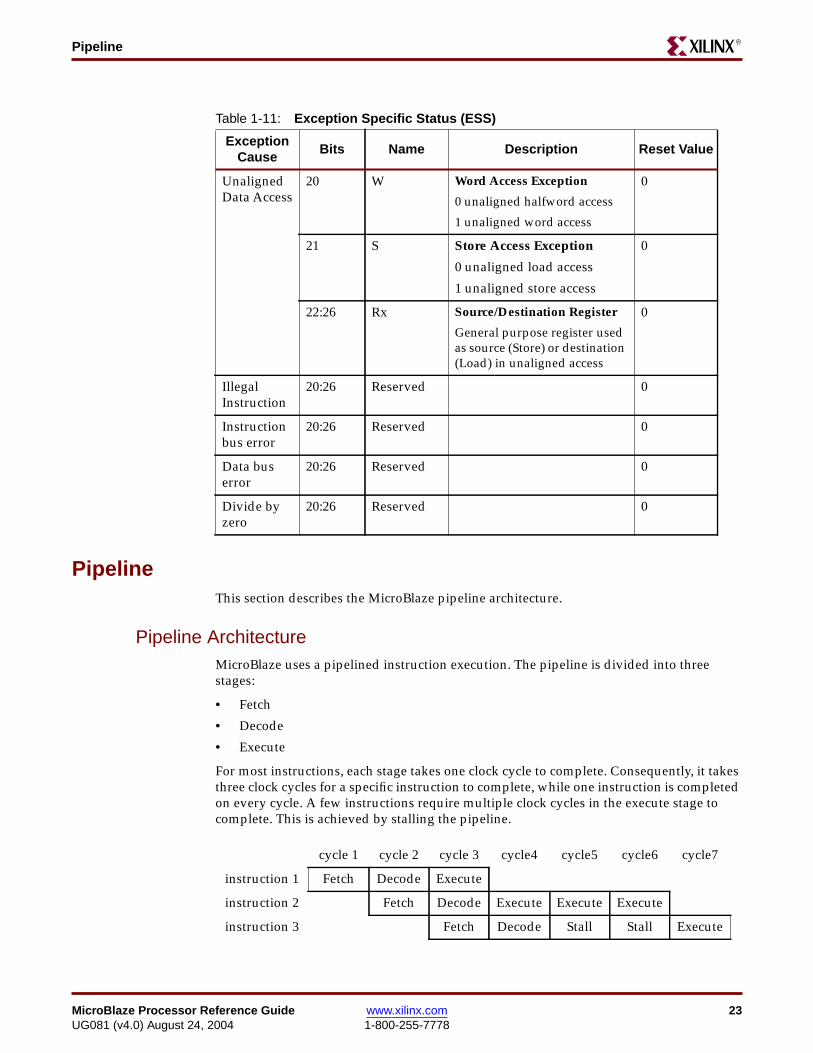
PipelineThis section describes the MicroBlaze pipeline architecture.
Pipeline ArchitectureMicroBlaze uses a pipelined instruction execution. The pipeline is divided into threestages:
• Fetch
• Decode
• Execute
For most instructions, each stage takes one clock cycle to complete. Consequently, it takesthree clock cycles for a specific instruction to complete, while one instruction is completedon every cycle. A few instructions require multiple clock cycles in the execute stage tocomplete. This is achieved by stalling the pipeline.
Table 1-11: Exception Specific Status (ESS)
ExceptionCause
Bits Name Description Reset Value
UnalignedData Access
20 W Word Access Exception
0 unaligned halfword access
1 unaligned word access
0
21 S Store Access Exception
0 unaligned load access
1 unaligned store access
0
22:26 Rx Source/Destination Register
General purpose register usedas source (Store) or destination(Load) in unaligned access
0
IllegalInstruction
20:26 Reserved 0
Instructionbus error
20:26 Reserved 0
Data buserror
20:26 Reserved 0
Divide byzero
20:26 Reserved 0
cycle 1 cycle 2 cycle 3 cycle4 cycle5 cycle6 cycle7
instruction 1 Fetch Decode Execute
instruction 2 Fetch Decode Execute Execute Execute
instruction 3 Fetch Decode Stall Stall Execute

24 www.xilinx.com MicroBlaze Processor Reference Guide1-800-255-7778 UG081 (v4.0) August 24, 2004
Chapter 1: MicroBlaze ArchitectureR
When executing from slower memory, instruction fetches may take multiple cycles. Thisadditional latency will directly affect the efficiency of the pipeline. MicroBlaze implementsan instruction prefetch buffer that reduces the impact of such multi-cycle instructionmemory latency. While the pipeline is stalled by a multi-cycle instruction in the executionstage the prefetch buffer continues to load sequential instructions. Once the pipelineresumes execution the fetch stage can load new instructions directly from the prefetchbuffer rather than having to wait for the instruction memory access to complete.
BranchesNormally the instructions in the fetch and decode stages (as well as prefetch buffer) areflushed when executing a taken branch. The fetch pipeline stage is then reloaded with anew instruction from the calculated branch address. A taken branch in MicroBlaze takesthree clock cycles to execute, two of which are required for refilling the pipeline. Tosomewhat mitigate this latency overhead, MicroBlaze supports branches with delay slots.
Delay Slots
When executing a taken branch with delay slot, only the fetch pipeline stage in MicroBlazeis flushed. The instruction in the decode stage (branch delay slot) is allowed to complete.This technique effectively reduces the branch penalty from two clock cycles to one. Branchinstructions with delay slots have a D appended to the instruction mnemonic. Forexample, the BNE instruction will not execute the subsequent instruction (does not have adelay slot), whereas BNED will execute the next instruction before control is transferred tothe branch location.
Memory ArchitectureMicroBlaze has a Harvard memory architecture, i.e. instruction and data accesses are donein separate address spaces. Each address space has a 32 bit range (i.e. handles up to 4GByte of instructions and data memory respectively). The instruction and data memoryranges can be made to overlap by mapping them both to the same physical memory. Thisis useful for e.g. software debugging.
Both instruction and data interfaces of MicroBlaze are 32 bit wide and use big endian(reverse bit order) format. MicroBlaze supports word, halfword and byte accesses to datamemory. Data accesses must be aligned (i.e. word accesses must be on word boundaries,halfword on halfword bounders), unless the processor is configured to support unalignedexceptions (available in MicroBlaze v3.00a and higher). All instruction accesses must beword aligned.
MicroBlaze does not separate between data accesses to I/O and memory (i.e. it usesmemory mapped I/O). The processor has up to three interfaces for memory accesses: LocalMemory Bus (LMB), On-Chip Peripheral Bus (OPB), and Xilinx CacheLink (XCL, onlyavailable in v3.00a or higher). The memory maps on these interfaces are mutuallyexclusive.
MicroBlaze uses speculative accesses to reduce latency over slower memory interfaces.This means that the processor will initiate each memory access on all available interfaces.When the correct interface has been resolved (i.e. matched against the interface addressmap) in the subsequent cycle, the other accesses are aborted.
For details on these different memory interfaces please refer to Chapter 2, “MicroBlazeSignal Interface Description”.

MicroBlaze Processor Reference Guide www.xilinx.com 25UG081 (v4.0) August 24, 2004 1-800-255-7778
Reset, Interrupts, Exceptions and BreakR
Reset, Interrupts, Exceptions and BreakAll versions of MicroBlaze supports reset, interrupt, user exception and break. Startingwith version 3.00a, MicroBlaze can also be configured to support hardware exceptions. Thefollowing section describes the execution flow associated with each of these events.
The relative priority starting with the highest is:
1. Reset
2. Hardware Exception
3. Non-maskable Break
4. Break
5. Interrupt
6. User Vector (Exception)
Table 1-12 defines the memory address locations of the associated vectors and thehardware enforced register file locations for return address. Each vector allocates twoaddresses to allow full address range branching (requires an IMM followed by a BRAIinstruction).
Reset
When a Reset or Debug_Rst(1) occurs, MicroBlaze will flush the pipeline and start fetching
instructions from the reset vector (address 0x0).
Equivalent Pseudocode
PC ← 0x00000000
Table 1-12: Vectors and Return Address Register File Location
Event Vector AddressRegister File
Return Address
Reset 0x00000000 -0x00000004 -
User Vector(Exception)
0x00000008 -0x0000000C -
Interrupt 0x00000010 -0x00000014 R14
Break: Non-maskable hardware
0x00000018 -0x0000001C R16Break: Hardware
Break
Break: Software
HardwareException
0x00000020 -0x00000024 R17
1. Reset input controlled by the XMD debugger via MDM

26 www.xilinx.com MicroBlaze Processor Reference Guide1-800-255-7778 UG081 (v4.0) August 24, 2004
Chapter 1: MicroBlaze ArchitectureR
MSR ← 0EAR ← 0ESR ← 0
InterruptMicroBlaze supports one external interrupt source (connecting to the Interrupt inputport). The processor will only react to interrupts if the interrupt enable (IE) bit in themachine status register (MSR) is set to 1. On an interrupt the instruction in the executionstage will complete, while the instruction in the decode stage is replaced by a branch to theinterrupt vector (address 0x10). The interrupt return address (the PC associated with theinstruction in the decode stage at the time of the interrupt) is automatically loaded intogeneral purpose register R14. In addition the processor also disables future interrupts byclearing the IE bit in the MSR.
Interrupts are ignored by the processor if the break in progress (BIP) bit in the MSR registeris set to 1.
Latency
The time it will take MicroBlaze to enter an Interrupt Service Routine (ISR) from the timean interrupt occurs, depends on the configuration of the processor. If MicroBlaze isconfigured to have a hardware divider, the largest latency will happen when an interruptoccurs during the execution of a division instruction.
Table 1-13 shows the different scenarios for interrupts. The cycle count includes the cyclesfor completing the current instruction, and branching to the service routine vector.
Equivalent Pseudocode
r14 ← PCPC ← 0x00000010MSR[IE] ← 0
User Vector (Exception)The user exception vector is located at address 0x8. A user exception is easiest caused byinserting a ‘BRAILD Rx,0x8’ instruction in the software flow. Although Rx could be anygeneral purpose register Xilinx recommends using R15 for storing the user exceptionreturn address, and to use the RTSD instruction to return from the user exception handler.
Pseudocode
rx ← PCPC ← 0x00000008
Table 1-13: Interrupt and Break latencies
ScenarioLMB Memory
VectorOPB Memory
Vector
Normally 4 cycles 6 cycles
Worst case without hardware divider 6 cycles 8 cycles
Worst case with hardware divider1
1. This does not take into account blocking FSL instructions which can stall indefinitly
37 cycles 39 cycles

MicroBlaze Processor Reference Guide www.xilinx.com 27UG081 (v4.0) August 24, 2004 1-800-255-7778
Reset, Interrupts, Exceptions and BreakR
Hardware ExceptionsMicroBlaze v3.00a and higher can be configured to detect different internal errorconditions: illegal instruction, instruction and data bus error, unaligned access and divideby zero. On a hardware exception MicroBlaze will flush the pipeline and branch to thehardware exception vector (address 0x20). The exception will also load the decode stageprogram counter value into the general purpose register R17. The execution stageinstruction in the exception cycle is not executed.
Equivalent Pseudocode
r17 ← PCPC ← 0x00000020MSR[EE] ← 0MSR[EIP] ← 1
BreaksThere are two kinds of breaks:
• Software (internal) breaks
• Hardware (external) breaks
Software Breaks
To perform a software break, use the brk and brki instructions. Refer to Chapter 4,“MicroBlaze Instruction Set Architecture” for detailed information on software breaks.
Hardware Breaks
Hardware breaks are performed by asserting the external break signal (i.e. the Ext_BRKand Ext_NM_BRK input ports). On a break the instruction in the execution stage willcomplete, while the instruction in the decode stage is replaced by a branch to the breakvector (address 0x18). The break return address (the PC associated with the instruction inthe decode stage at the time of the break) is automatically loaded into general purposeregister R16.MicroBlaze also sets the Break In Progress (BIP) flag in the Machine StatusRegister (MSR).
A normal hardware break (i.e the Ext_BRK input port) is only handled when there is nobreak in progress (i.e MSR[BIP] is set to 0). The Break In Progress flag also disablesinterrupts and exceptions. A non-maskable break (i.e the Ext_NM_BRK input port) willalways be handled immediately.
Latency
The time it will take MicroBlaze to enter a break service routine from the time the breakoccurs, depends on the instruction currently in the execution stage.
Table 1-13 shows the different scenarios for breaks. The cycle count includes the cycles forcompleting the current instruction, and branching to the service routine vector.
Equivalent Pseudocode
r16 ← PCPC ← 0x00000018MSR[BIP] ← 1

28 www.xilinx.com MicroBlaze Processor Reference Guide1-800-255-7778 UG081 (v4.0) August 24, 2004
Chapter 1: MicroBlaze ArchitectureR
Instruction Cache
OverviewMicroBlaze may be used with an optional instruction cache for improved performancewhen executing code that resides outside the LMB address range.
The instruction cache has the following features
• Direct mapped (1-way associative)
• User selectable cacheable memory area
• Configurable cache size
• Configurable caching over OPB or CacheLink
• 4 word cache-line (only with CacheLink)
• Individual cache line lock capability
• Cache on and off controlled using a new bit in the MSR register
• Instructions to write to the instruction cache
• Memory is organized into a cacheable and a non-cacheable segment
Instruction Cache OrganizationMicroBlaze can be configured to cache instructions over either the OPB interface, or thededicated Xilinx CacheLink interface (only available in MicroBlaze v3.00a and higher). Thechoice is determined by the setting of the two parameters: C_USE_ICACHE andC_ICACHE_USE_FSL (for details see: “MicroBlaze Core Configurability” in Chapter 2).The main differences between the two solutions are:
• Caching over CacheLink uses 4 word cache lines (critical word first). OPB caches usesingle word cache lines.
• The CacheLink interface requires a specialized memory controller interface. The OPBinterface uses standard OPB memory controllers.
For details on the CacheLink interface on MicroBlaze, please refer to “Xilinx CacheLink(XCL) Interface Description” in Chapter 2.
General Instruction Cache FunctionalityWhen the instruction cache is used, the memory address space in split into two segments -a cacheable segment and a non-cacheable segment. The cacheable segment is determinedby two parameters, C_ICACHE_BASEADDR and C_ICACHE_HIGHADDR. Alladdresses within this range correspond to the cacheable address space segment. All otheraddresses are non-cacheable.

MicroBlaze Processor Reference Guide www.xilinx.com 29UG081 (v4.0) August 24, 2004 1-800-255-7778
Instruction CacheR
Cacheable instruction addresses are further split into two segments - a cache word addresssegment and a tag address segment. The size of the two segments can be configured by theuser. The size of the cache word address can be between 7 to 14 bits. This results in cachesizes ranging from 512B to 64 kB(1). The tag address should be sized so that it matches thecomplete range of cacheable memory in the design. E.g. assuming a configuration ofC_ICACHE_BASEADDR= 0x00300000, C_ICACHE_HIGHADDR=0x0030ffff, andC_ICACHE_BYTE_SIZE=4096; the cacheable byte address range is 16 bits, and the cachebyte address range is 12 bits (i.e. a 10 bit cache word address), thus the required address tagis: 16-12=4 bits.
Instruction Cache OperationFor every instruction fetched, the instruction cache detects if the instruction addressbelongs to the cacheable segment. If the address is non-cacheable, the cache ignores theinstruction and allows the OPB to fulfill the request. If the address is cacheable, a lookup isperformed on the tag memory to check if the requested instruction is in the cache. Thelookup is successful when both the valid bit is set and the tag address is the same as the tagaddress segment of the instruction address.
Figure 1-7: OPB Instruction Cache Organization(CacheLink is similar but uses 4 word cache lines)
1. The size of the cache is FPGA architecture dependent. The MicroBlaze instruction cache can be configured touse between 1 and 32 RAMB primitives. The actual cache size therefore depends on the RAMB size in thetargeted architecture.
Instruction Address Bits0 30 31
Cache Word AddressTag Address --
Tag
Instruction BRAM
BRAMAddr
Addr
=Tag
ValidCache_Hit
Cache_instruction_data

30 www.xilinx.com MicroBlaze Processor Reference Guide1-800-255-7778 UG081 (v4.0) August 24, 2004
Chapter 1: MicroBlaze ArchitectureR
If the instruction is in the cache, the cache will drive the ready signal (Cache_Hit) forMicroBlaze and the instruction data for the address. If the instruction is not in the cache,the cache will not drive the ready signal but will wait until the OPB fulfills the request andupdates the cache with the new information.
Instruction Cache Software Support
MSR Bit
Bit 26 in the MSR indicates whether or not the cache is enabled. The MFS and MTSinstructions are used to read and write to the MSR respectively.
The contents of the cache are preserved by default when the cache is disabled. The usermay overwrite the contents of the cache using the WIC instruction or using the hardwaredebug logic of MicroBlaze.
WIC Instruction
The WIC instruction may be used to update the instruction cache from a softwareprogram. For a detailed description, please refer to Chapter 4, “MicroBlaze Instruction SetArchitecture”.
HW Debug Logic
The HW debug logic may be used to perform a similar operation as the WIC instruction.
Lock Bit
The lock bit can be used to permanently lock a code segment into the cache and thereforeguarantee the instruction execution time. Locking of the cacheline however may result in adecrease in the number of cache hits. This is because there could be addresses that were notcached as the cacheline is locked.
The use of instruction LMB in most cases would be a better choice for locking codesegments since the wait states for accessing the LMB is the same as for cache hits.
Figure 1-8: Cache Operation
IOPB_Address
IOPB_Data
Cache Line
Tag Address
0,1 (Locked,Valid)
Instruction BRAM
Tag BRAM
Data
Data
Address
Address
WE
WE
IOPB_XferAck
0 1
IOPB_Select

MicroBlaze Processor Reference Guide www.xilinx.com 31UG081 (v4.0) August 24, 2004 1-800-255-7778
Data CacheR
Data Cache
OverviewMicroBlaze may be used with an optional data cache for improved performance whenreading data that resides outside the LMB address range.
The data cache has the following features
• Direct mapped (1-way associative)
• Write-through
• User selectable cacheable memory area
• Configurable cache size and tag size
• Configurable caching over OPB or CacheLink
• 4 word cache-line (only with CacheLink)
• Individual cache line lock capability
• Cache on and off controlled using a new bit in the MSR register
• Instructions to write to the data cache
• Memory is organized into a cacheable and a non-cacheable segments
Data Cache OrganizationMicroBlaze can be configured to cache data over either the OPB interface, or the dedicatedXilinx CacheLink interface (only available in MicroBlaze v3.00a and higher). The choice isdetermined by the setting of the two parameters: C_USE_DCACHE andC_DCACHE_USE_FSL (for details see: “MicroBlaze Core Configurability” in Chapter 2).The main differences between the two solutions are:
• Caching over CacheLink uses 4 word cache lines (critical word first). OPB caches usesingle word cache lines.
• The CacheLink interface requires a specialized memory controller interface. The OPBinterface uses standard OPB memory controllers.
For details on the CacheLink interface on MicroBlaze, please refer to “Xilinx CacheLink(XCL) Interface Description” in Chapter 2.
General Data Cache FunctionalityWhen the data cache is used, the memory address space in split into two segments - acacheable segment and a non-cacheable segment. The cacheable area is determined by twoparameters, C_DCACHE_BASEADDR and C_DCACHE_HIGHADDR. All addresseswithin this range correspond to the cacheable address space. All other addresses are non-cacheable.

32 www.xilinx.com MicroBlaze Processor Reference Guide1-800-255-7778 UG081 (v4.0) August 24, 2004
Chapter 1: MicroBlaze ArchitectureR
All cacheable data addresses are further split into two segments - a cache word addresssegment and a tag address segment. The size of the two segments can be configured by theuser. The size of the cache word address can be between 9 to 14 bits. This results in a cachesizes ranging from 2 kB to 64 kB(1). The tag address should be sized so that it matches thecomplete range of cacheable memory in the design. E.g. assuming a configuration ofC_DCACHE_BASEADDR= 0x00400000, C_DCACHE_HIGHADDR=0x00403fff, andC_DCACHE_BYTE_SIZE=2048; the cacheable byte address range is 14 bits, and the cachebyte address range is 11 bits (i.e. a 9 bit cache word address), thus the required address tagis 14-11=3 bits.
Data Cache OperationWhen MicroBlaze executes a store instruction, the operation is performed as normal but ifthe address is within the cacheable address segment, the data cache is updated with thenew data, i.e. the cache is not loaded on a write miss.
When MicroBlaze executes a load instruction, the address is first checked to see if theaddress is within the cacheable area and secondly if the address is in the data cache. If thatcase, the data is fetch from the data cache.
Figure 1-9: OPB Data Cache Organization(CacheLink is similar but uses 4 word cache lines)
1. The size of the cache is FPGA architecture dependent. The MicroBlaze data cache can be configured to usebetween 4 and 32 RAMB primitives. The actual cache size therefore depends on the RAMB size in the targetedarchitecture.
Data Address Bits0 30 31
Cache Word AddressTag Address --
Tag
Data BRAM
BRAMAddr
Addr
=Tag
ValidCache_Hit
Cache data
Load_Instruction

MicroBlaze Processor Reference Guide www.xilinx.com 33UG081 (v4.0) August 24, 2004 1-800-255-7778
Data CacheR
If the read data is in the cache, the cache will drive the ready signal (Cache_Hit) forMicroBlaze and the data for the address. If the read data is not in the cache, the cache willnot drive the ready signal but will:
• for OPB caching; wait until the OPB fulfills the speculative read request
• for CacheLink caching; send a cache line request over the CacheLink interface.
Data Cache Software Support
MSR Bit
Bit 24 in the MSR indicates whether or not the cache is enabled. The MFS and MTSinstructions are used to read and write to the MSR respectively.
The contents of the cache are preserved by default when the cache is disabled. The cachecannot be turned on/off from an interrupt handler routine as the changes to the MSR is lostonce the interrupt is handled (the MSR state is restored after interrupt handling).
WDC Instruction
The WDC instruction may be used to update the data cache from a software program. Fora detailed description, please refer to Chapter 4, “MicroBlaze Instruction Set Architecture”.
HW Debug Logic
The HW debug logic may be used to perform a similar operation as the WDC instruction.
Lock Bit
The lock bit can be used to permanently lock a code segment into the cache and thereforeguarantee that this data is always in the cache. Locking of the cacheline however mayresult in a decrease in the number of cache hits. This is because there could be addressesthat were not cached as the cacheline is locked.
The use of data LMB in most cases would be a better choice for locking data since the waitstates for accessing the LMB is the same as for cache hits.
Figure 1-10: Data Cache Operation
DOPB_Address
DOPB_Data
Cache Line
Tag Address
0,1 (Locked,Valid)
Instruction BRAM
Tag BRAM
Data
Data
Address
Address
WE
WE
DOPB_XferAckDOPB_Select
DOPB_RNW
Cacheable_address

34 www.xilinx.com MicroBlaze Processor Reference Guide1-800-255-7778 UG081 (v4.0) August 24, 2004
Chapter 1: MicroBlaze ArchitectureR
Fast Simplex Link (FSL)MicroBlaze contains eight Fast Simplex Link (FSL) interfaces, each consisting of one inputand one output port. The FSL channels are dedicated uni-directional point-to-point datastreaming interfaces. For detailed information on the FSL interface, please refer to the FSLBus data sheet (DS449).
The FSL interfaces on MicroBlaze are 32 bits wide. A separate bit indicates whether thesent/received word is of control or data type. The get instruction in MicroBlaze ISA usedto transfer information from an FSL port to a general purpose register. The put instructionis used for transfer in the opposite direction. Both instructions come in 4 flavours: blockingdata, non-blocking data, blocking control, and non-blocking control. For a detaileddescription of the get and put instructions please refer to Chapter 4, “MicroBlazeInstruction Set Architecture”.
Hardware Acceleration using FSLEach FSL provides a low latency dedicated interface to the processor pipeline. Thus theyare ideal for extending the processors execution unit with custom hardware accelerators. Asimple example is illustrated in Figure 1-11.
Figure 1-11: FSL used with HW accelerated function fx
This method is similar to extending the ISA with custom instructions, but has the benefit ofnot making the overall speed of processor pipeline dependent on the custom function.Also, there are no additional requirements on the software tool chain associated with thistype of functional extension.
Debug and Trace
Debug OverviewMicroBlaze features a debug interface to support JTAG based software debugging tools(commonly known as BDM or Background Debug Mode debuggers) like the XilinxMicroprocessor Debug (XMD) tool. The debug interface is designed to be connected to theXilinx Microprocessor Debug Module (MDM) core, which interfaces with the JTAG port ofXilinx FPGAs. Multiple MicroBlaze instances can be interfaced with a single MDM toenable multiprocessor debugging. The debugging features include:
MicroBlaze
Custom HW AcceleratorFSLx// Configure fx
cput FSLx, Rc
// Store operands
put FSLx, Ra // op 1
put FSLx, Rb // op 2
// Load result
get FSLx, Rt
Example code:
RegisterFile
ConfigReg
Op1Reg Op2Reg
fxResultReg
FSLx

MicroBlaze Processor Reference Guide www.xilinx.com 35UG081 (v4.0) August 24, 2004 1-800-255-7778
Debug and TraceR
• Configurable number of hardware breakpoints and watchpoints and unlimitedsoftware breakpoints
• External processor control enables debug tools to stop, reset and single stepMicroBlaze
• Read and write memory and all registers including PC and MSR
• Support for multiple processors
• Write to Instruction and data cache
Trace OverviewThe MicroBlaze trace interface exports a number of internal state signals for performancemonitoring and analysis. Xilinx recommends that users only use the trace interfacethrough Xilinx developed analysis cores. This interface is not guaranteed to be backwardcompatible in future releases of MicroBlaze.

36 www.xilinx.com MicroBlaze Processor Reference Guide1-800-255-7778 UG081 (v4.0) August 24, 2004
Chapter 1: MicroBlaze ArchitectureR
MicroBlaze Processor Reference Guide www.xilinx.com 37UG081 (v4.0) August 24, 2004 1-800-255-7778
R
Chapter 2
MicroBlaze Signal Interface Description
OverviewThe MicroBlaze core is organized as a Harvard architecture with separate bus interfaceunits for data accesses and instruction accesses. The following tree memory interfaces aresupported: Local Memory Bus (LMB), IBM’s On-chip Peripheral Bus (OPB) and XilinxCacheLink (XCL, only in MicroBlaze v3.00a and higher). The LMB provides single-cycleaccess to on-chip dual-port block RAM. The OPB interface provides a connection to bothon-and off-chip peripherals and memory. The CacheLink interface is intended for use withspecialized external memory controllers. MicroBlaze also supports up to 8 Fast SimplexLink (FSL) ports, each with one master and one slave FSL interface.
FeaturesThe MicroBlaze bus interfaces include the following features:
• OPB V2.0 bus interface with byte-enable support (see IBM’s 64-Bit On-Chip PeripheralBus, Architectural Specifications, Version 2.0)
• LMB provides simple synchronous protocol for efficient block RAM transfers
• FSL provides a fast non-arbitrated streaming communication mechanism
• XCL provides a fast slave-side arbitrated streaming interface between caches andspecialized external memory controller
• Debug interface for use with the Microprocessor Debug Module (MDM) core
• Trace interface for performance analysis
MicroBlaze I/O OverviewThe core interfaces shown in Figure 2-1 and the following Table 2-1 are defined as follows:
DOPB: Data interface, On-chip Peripheral BusDLMB: Data interface, Local Memory Bus (BRAM only)IOPB: Instruction interface, On-chip Peripheral BusILMB: Instruction interface, Local Memory Bus (BRAM only)MFSL 0..7: FSL master interfaceSFSL 0..7: FSL slave interfaceIXCL: Instruction side Xilinx CacheLink interface (FSL master/slave pair)DXCL: Data side Xilinx CacheLink interface (FSL master/slave pair)Core: Miscellaneous signals for clock, reset, debug and trace

38 www.xilinx.com MicroBlaze Processor Reference Guide1-800-255-7778 UG081 (v4.0) August 24, 2004
Chapter 2: MicroBlaze Signal Interface DescriptionR
Figure 2-1: MicroBlaze Core Block Diagram
Data-sideInstruction-side
DOPB
DLMB
IOPB
ILMB
bus interface bus interface
InstructionBuffer
ProgramCounter
Register File32 X 32b
Add/Sub
Shift/Logical
Multiply
InstructionDecode
BusIF
BusIF
MFSL 0..7
SFSL 0..7
DXCL_M
DXCL_S
IXCL_M
IXCL_S
I-Cache
D-C
ache
Table 2-1: Summary of MicroBlaze Core I/O
Signal Interface I/O Description
DM_ABus[0:31] DOPB O Data interface OPB address bus
DM_BE[0:3] DOPB O Data interface OPB byte enables
DM_busLock DOPB O Data interface OPB buslock
DM_DBus[0:31] DOPB O Data interface OPB write data bus
DM_request DOPB O Data interface OPB bus request
DM_RNW DOPB O Data interface OPB read, not write
DM_select DOPB O Data interface OPB select
DM_seqAddr DOPB O Data interface OPB sequential address
DOPB_DBus[0:31] DOPB I Data interface OPB read data bus
DOPB_errAck DOPB I Data interface OPB error acknowledge
DOPB_MGrant DOPB I Data interface OPB bus grant
DOPB_retry DOPB I Data interface OPB bus cycle retry
DOPB_timeout DOPB I Data interface OPB timeout error
DOPB_xferAck DOPB I Data interface OPB transferacknowledge
IM_ABus[0:31] IOPB O Instruction interface OPB address bus
IM_BE[0:3] IOPB O Instruction interface OPB byte enables
IM_busLock IOPB O Instruction interface OPB buslock
IM_DBus[0:31] IOPB O Instruction interface OPB write data bus(always 0x00000000)
IM_request IOPB O Instruction interface OPB bus request

MicroBlaze Processor Reference Guide www.xilinx.com 39UG081 (v4.0) August 24, 2004 1-800-255-7778
MicroBlaze I/O OverviewR
IM_RNW IOPB O Instruction interface OPB read, not write(tied to ’0’)
IM_select IOPB O Instruction interface OPB select
IM_seqAddr IOPB O Instruction interface OPB sequentialaddress
IOPB_DBus[0:31] IOPB I Instruction interface OPB read data bus
IOPB_errAck IOPB I Instruction interface OPB erroracknowledge
IOPB_MGrant IOPB I Instruction interface OPB bus grant
IOPB_retry IOPB I Instruction interface OPB bus cycle retry
IOPB_timeout IOPB I Instruction interface OPB timeout error
IOPB_xferAck IOPB I Instruction interface OPB transferacknowledge
Data_Addr[0:31] DLMB O Data interface LB address bus
Byte_Enable[0:3] DLMB O Data interface LB byte enables
Data_Write[0:31] DLMB O Data interface LB write data bus
D_AS DLMB O Data interface LB address strobe
Read_Strobe DLMB O Data interface LB read strobe
Write_Strobe DLMB O Data interface LB write strobe
Data_Read[0:31] DLMB I Data interface LB read data bus
DReady DLMB I Data interface LB data ready
Instr_Addr[0:31] ILMB O Instruction interface LB address bus
I_AS ILMB O Instruction interface LB address strobe
IFetch ILMB O Instruction interface LB instruction fetch
Instr[0:31] ILMB I Instruction interface LB read data bus
IReady ILMB I Instruction interface LB data ready
FSL0_M .. FSL7_M MFSL O Master interface to Output FSL channels
FSL0_S .. FSL7_S SFSL I Slave interface to Input FSL channels
ICache_FSL_in... IXCL_S IO Instruction side CacheLink FSL slaveinterface
ICache_FSL_out... IXCL_M IO Instruction side CacheLink FSL masterinterface
DCache_FSL_in... DXCL_S IO Data side CacheLink FSL slave interface
DCache_FSL_out... DXCL_M IO Data side CacheLink FSL masterinterface
Interrupt Core I Interrupt
Table 2-1: Summary of MicroBlaze Core I/O (Continued)
Signal Interface I/O Description

40 www.xilinx.com MicroBlaze Processor Reference Guide1-800-255-7778 UG081 (v4.0) August 24, 2004
Chapter 2: MicroBlaze Signal Interface DescriptionR
On-Chip Peripheral Bus (OPB) Interface DescriptionThe MicroBlaze OPB interfaces are organized as byte-enable capable only masters. Thebyte-enable architecture is an optional subset of the OPB V2.0 specification and is ideal forlow-overhead FPGA implementations such as MicroBlaze.
The OPB data bus interconnects are illustrated in Figure 2-2. The write data bus (frommasters and bridges) is separated from the read data bus (from slaves and bridges) tobreak up the bus OR logic. In minimal cases this can completely eliminate the OR logic forthe read or write data buses. Optionally, you can "OR" together the read and write buses tocreate the correct functionality for the OPB bus monitor. Note that the instruction-side OPBcontains a write data bus (tied to 0x00000000) and a RNW signal (tied to logic 1) so that itsinterface remains consistent with the data-side OPB. These signals are constant andgenerally are minimized in implementation.
A multi-ported slave is used instead of a bridge in the example shown in Figure 2-3. Thiscould represent a memory controller with a connection to both the IOPB and the DOPB. Inthis case, the bus multiplexing and prioritization must be done in the slave. The advantageof this approach is that a separate I-to-D bridge and an OPB arbiter on the instruction sideare not required. The arbiter function must still exist in the slave device.
Reset Core I Core reset
Clk Core I Clock
Debug_Rst Core I Reset signal from OPB JTAG UART
Ext_BRK Core I Break signal from OPB JTAG UART
Ext_NM_BRK Core I Non-maskable break signal from OPBJTAG UART
Dbg_... Core IO Debug signals from OPB MDM
Valid_Instr Core O Trace signals for real time HW analysis
PC_Ex Core O Trace signals for real time HW analysis
Reg_Write Core O Trace signals for real time HW analysis
Reg_Addr Core O Trace signals for real time HW analysis
MSR_Reg Core O Trace signals for real time HW analysis
New_Reg_Value Core O Trace signals for real time HW analysis
Pipe_Running Core O Trace signals for real time HW analysis
Interrup_Taken Core O Trace signals for real time HW analysis
Jump_Taken Core O Trace signals for real time HW analysis
Prefetch_Addr Core O Trace signals for real time HW analysis
MB_Halted Core O Trace signals for real time HW analysis
Trace_... Core O Trace signals for real time HW analysis
Table 2-1: Summary of MicroBlaze Core I/O (Continued)
Signal Interface I/O Description

MicroBlaze Processor Reference Guide www.xilinx.com 41UG081 (v4.0) August 24, 2004 1-800-255-7778
On-Chip Peripheral Bus (OPB) Interface DescriptionR
Figure 2-2: OPB Interconnection (breaking up read and write buses)
DM_ABus[0:31]DM_BE[0:3]DM_busLockDM_wrDBus[0:31]DM_RNWDM_selectDM_seqAddr
DOPB_ABus[0:31]DOPB_BE[0:3]DOPB_busLockDOPB_wrDBus[0:31]
DOPB_RNWDOPB_selectDOPB_seqAddrDOPB_errAckDOPB_retryDOPB_timeoutDOPB_toutSupDOPB_xferAck
DOPB_ABus[0:31]DOPB_BE[0:3]DOPB_busLock
DOPB_rdDBus[0:31]
DOPB_RNWDOPB_selectDOPB_seqAddr
DOPB_errAckDOPB_retryDOPB_timeoutDOPB_xferAck
DOPB_wrDBus[0:31]
Sl1_rdDBus[0:31]Sl1_errAckSl1_retrySl1_timeoutSl1_toutSupSl1_xferAck
DOPB_ABus[0:31]DOPB_BE[0:3]DOPB_busLock
DOPB_RNWDOPB_selectDOPB_seqAddr
DOPB_wrDBus[0:31]
Br1I_rdDBus[0:31]Br1_errAckBr1_retryBr1_timeout
Br1_ABus[0:31]Br1_BE[0:3]Br1_busLockBr1D_wrDBus[0:31]Br1_RNWBr1_selectBr1_seqAddr
IOPB_rdDBus[0:31]IOPB_errAckIOPB_retryIOPB_timeoutIOPB_toutSup
IM_ABus[0:31]IM_BE[0:3]IM_busLock
IM_RNWIM_selectIM_seqAddr
IOPB_rdDBus[0:31]IOPB_errAckIOPB_retryIOPB_timeoutIOPB_xferAck
IOPB_ABus[0:31]IOPB_BE[0:3]IOPB_busLock
IOPB_RNWIOPB_selectIOPB_seqAddr
IOPB_wrDBus[0:31]
Sl2_rdDBus[0:31]Sl2_errAckSl2_retrySl2_timeoutSl2_toutSupSl2_xferAck
IOPB_ABus[0:31]IOPB_BE[0:3]IOPB_busLockIOPB_wrDBus[0:31]
IOPB_RNWIOPB_selectIOPB_seqAddrIOPB_errAckIOPB_retryIOPB_timeoutIOPB_toutSupIOPB_xferAck
Br1_toutSup
MicroBlazeData OPBInterface
OPBSlave1
MicroBlazeInstr OPBInterface
(IOPB)
OPBSlave2
DOPBto
IOPB
OR
like
suffixes
OR
like
suffixes
DOPB_rdDBus[0:31]
IOPB_rdDBus[0:31]
ORIOPB_wrDBus[0:31]IOPB_rdDBus[0:31]
IOPB_DBus[0:31]
ORDOPB_wrDBus[0:31]DOPB_rdDBus[0:31]
DOPB_DBus[0:31]
Present for Bus Monitor functions:
Present for Bus Monitor functions:
Data-side OPB
Instruction-side OPB
I-sideOPB
arbiter
D-sideOPB
arbiter
Required if more thanone master present
Required
Br1_xferAckIOPB_xferAck
IM_wrDBus[0:31]
DM_requestDOPB_MGrant
IM_requestIOPB_MGrant
Br1_requestBr1_MGrant

42 www.xilinx.com MicroBlaze Processor Reference Guide1-800-255-7778 UG081 (v4.0) August 24, 2004
Chapter 2: MicroBlaze Signal Interface DescriptionR
Figure 2-3: OPB Interconnection (with multi-ported slave and no bridge)
DM_ABus[0:31]DM_BE[0:3]DM_busLockDM_wrDBus[0:31]DM_RNWDM_selectDM_seqAddr
DOPB_ABus[0:31]DOPB_BE[0:3]DOPB_busLockDOPB_wrDBus[0:31]
DOPB_RNWDOPB_selectDOPB_seqAddrDOPB_errAckDOPB_retryDOPB_timeoutDOPB_toutSupDOPB_xferAck
DOPB_ABus[0:31]DOPB_BE[0:3]DOPB_busLock
DOPB_rdDBus[0:31]
DOPB_RNWDOPB_selectDOPB_seqAddr
DOPB_errAckDOPB_retryDOPB_timeoutDOPB_xferAck
DOPB_wrDBus[0:31]
Sl1_rdDBus[0:31]Sl1_errAckSl1_retrySl1_timeoutSl1_toutSupSl1_xferAck
DOPB_ABus[0:31]DOPB_BE[0:3]DOPB_busLock
DOPB_RNWDOPB_selectDOPB_seqAddr
DOPB_wrDBus[0:31]
IM_ABus[0:31]IM_BE[0:3]IM_busLock
IM_RNWIM_selectIM_seqAddr
IOPB_rdDBus[0:31]IOPB_errAckIOPB_retryIOPB_timeoutIOPB_xferAck
IOPB_ABus[0:31]IOPB_BE[0:3]IOPB_busLock
IOPB_RNWIOPB_selectIOPB_seqAddr
IOPB_wrDBus[0:31]
Sl2_rdDBus[0:31]Sl2_errAckSl2_retrySl2_timeoutSl2_toutSupSl2_xferAck
IOPB_ABus[0:31]IOPB_BE[0:3]IOPB_busLockIOPB_wrDBus[0:31]
IOPB_RNWIOPB_selectIOPB_seqAddrIOPB_errAckIOPB_retryIOPB_timeoutIOPB_toutSupIOPB_xferAck
MicroBlazeData OPBInterface
OPBSlave1
MicroBlazeInstr OPBInterface
OR
like
suffixes
OR
like
suffixes
DOPB_rdDBus[0:31]
IOPB_rdDBus[0:31]
ORIOPB_wrDBus[0:31]IOPB_rdDBus[0:31]
IOPB_DBus[0:31]
ORDOPB_wrDBus[0:31]DOPB_rdDBus[0:31]
DOPB_DBus[0:31]
Present for Bus Monitor functions:
Present for Bus Monitor functions:
Data-side OPB
Instruction-side OPB
Sl2_rdDBus[0:31]Sl2_errAckSl2_retrySl2_timeoutSl2_toutSupSl2_xferAck
OPBSlave2(multi-
D-sideOPB
arbiter
Required if more thanone master present
DM_requestDOPB_MGrant
IM_requestIOPB_MGrant

MicroBlaze Processor Reference Guide www.xilinx.com 43UG081 (v4.0) August 24, 2004 1-800-255-7778
Local Memory Bus (LMB) Interface DescriptionR
Local Memory Bus (LMB) Interface DescriptionThe LMB is a synchronous bus used primarily to access on-chip block RAM. It uses aminimum number of control signals and a simple protocol to ensure that local block RAMis accessed in a single clock cycle. LMB signals and definitions are shown in the followingtable. All LMB signals are active high.
LMB Signal Interface
Addr[0:31]
The address bus is an output from the core and indicates the memory address that is beingaccessed by the current transfer. It is valid only when AS is high. In multicycle accesses(accesses requiring more than one clock cycle to complete), Addr[0:31] is valid only in thefirst clock cycle of the transfer.
Byte_Enable[0:3]
The byte enable signals are outputs from the core and indicate which byte lanes of the databus contain valid data. Byte_Enable[0:3] is valid only when AS is high. In multicycleaccesses (accesses requiring more than one clock cycle to complete), Byte_Enable[0:3] isvalid only in the first clock cycle of the transfer. Valid values for Byte_Enable[0:3] areshown in the following table:
Table 2-2: LMB Bus Signals
Signal Data InterfaceInstructionInterface
Type Description
Addr[0:31] Data_Addr[0:31] Instr_Addr[0:31] O Address bus
Byte_Enable[0:3] Byte_Enable[0:3] not used O Byte enables
Data_Write[0:31] Data_Write[0:31] not used O Write data bus
AS D_AS I_AS O Address strobe
Read_Strobe Read_Strobe IFetch O Read in progress
Write_Strobe Write_Strobe not used O Write in progress
Data_Read[0:31] Data_Read[0:31] Instr[0:31] I Read data bus
Ready DReady IReady I Ready for next transfer
Clk Clk Clk I Bus clock
Table 2-3: Valid Values for Byte_Enable[0:3]
Byte Lanes Used
Byte_Enable[0:3] Data[0:7] Data[8:15] Data[16:23] Data[24:31]
0000
0001 x
0010 x
0100 x

44 www.xilinx.com MicroBlaze Processor Reference Guide1-800-255-7778 UG081 (v4.0) August 24, 2004
Chapter 2: MicroBlaze Signal Interface DescriptionR
Data_Write[0:31]
The write data bus is an output from the core and contains the data that is written tomemory. It becomes valid when AS is high and goes invalid in the clock cycle after Readyis sampled high. Only the byte lanes specified by Byte_Enable[0:3] contain valid data.
AS
The address strobe is an output from the core and indicates the start of a transfer andqualifies the address bus and the byte enables. It is high only in the first clock cycle of thetransfer, after which it goes low and remains low until the start of the next transfer.
Read_Strobe
The read strobe is an output from the core and indicates that a read transfer is in progress.This signal goes high in the first clock cycle of the transfer, and remains high until the clockcycle after Ready is sampled high. If a new read transfer is started in the clock cycle afterReady is high, then Read_Strobe remains high.
Write_Strobe
The write strobe is an output from the core and indicates that a write transfer is in progress.This signal goes high in the first clock cycle of the transfer, and remains high until the clockcycle after Ready is sampled high. If a new write transfer is started in the clock cycle afterReady is high, then Write_Strobe remains high.
Data_Read[0:31]
The read data bus is an input to the core and contains data read from memory.Data_Read[0:31] is valid on the rising edge of the clock when Ready is high.
Ready
The Ready signal is an input to the core and indicates completion of the current transferand that the next transfer can begin in the following clock cycle. It is sampled on the risingedge of the clock. For reads, this signal indicates the Data_Read[0:31] bus is valid, and forwrites it indicates that the Data_Write[0:31] bus has been written to local memory.
Clk
All operations on the LMB are synchronous to the MicroBlaze core clock.
1000 x
0011 x x
1100 x x
1111 x x x x
Table 2-3: Valid Values for Byte_Enable[0:3]
Byte Lanes Used
Byte_Enable[0:3] Data[0:7] Data[8:15] Data[16:23] Data[24:31]

MicroBlaze Processor Reference Guide www.xilinx.com 45UG081 (v4.0) August 24, 2004 1-800-255-7778
Local Memory Bus (LMB) Interface DescriptionR
LMB TransactionsThe following diagrams provide examples of LMB bus operations.
Generic Write Operation
Generic Read Operation
Figure 2-4: LMB Generic Write Operation
Clk
Addr
Byte_Enable
Data_Write
AS
Read_Strobe
Write_Strobe
Data_Read
Ready
A0
1111
D0
Figure 2-5: LMB Generic Read Operation
Clk
Addr
Byte_Enable
Data_Write
AS
Read_Strobe
Write_Strobe
Data_Read
Ready
A0
1111
D0

46 www.xilinx.com MicroBlaze Processor Reference Guide1-800-255-7778 UG081 (v4.0) August 24, 2004
Chapter 2: MicroBlaze Signal Interface DescriptionR
Back-to-Back Write Operation (Typical LMB access - 2 clocks per write)
Single Cycle Back-to-Back Read Operation (Typical I-side access - 1 clockper read)
Figure 2-6: LMB Back-to-Back Write Operation
Figure 2-7: LMB Single Cycle Back-to-Back Read Operation
Clk
Addr
Byte_Enable
Data_Write
AS
Read_Strobe
Write_Strobe
Data_Read
Ready
A0 A1
BE0 BE1
D0 D1
Clk
Addr
Byte_Enable
Data_Write
AS
Read_Strobe
Write_Strobe
Data_Read
Ready
A0 A1 A2
BE0 BE1 BE2
D0 D1 D2
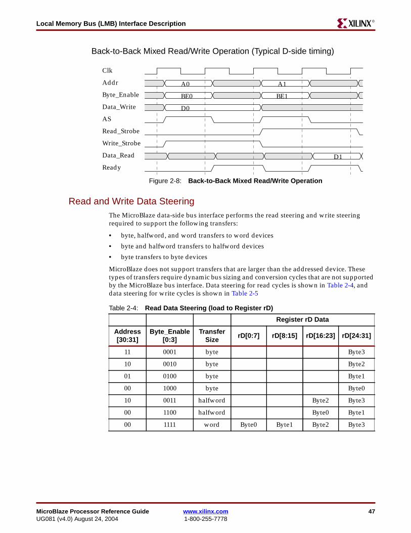
MicroBlaze Processor Reference Guide www.xilinx.com 47UG081 (v4.0) August 24, 2004 1-800-255-7778
Local Memory Bus (LMB) Interface DescriptionR
Back-to-Back Mixed Read/Write Operation (Typical D-side timing)
Read and Write Data SteeringThe MicroBlaze data-side bus interface performs the read steering and write steeringrequired to support the following transfers:
• byte, halfword, and word transfers to word devices
• byte and halfword transfers to halfword devices
• byte transfers to byte devices
MicroBlaze does not support transfers that are larger than the addressed device. Thesetypes of transfers require dynamic bus sizing and conversion cycles that are not supportedby the MicroBlaze bus interface. Data steering for read cycles is shown in Table 2-4, anddata steering for write cycles is shown in Table 2-5
Figure 2-8: Back-to-Back Mixed Read/Write Operation
Clk
Addr
Byte_Enable
Data_Write
AS
Read_Strobe
Write_Strobe
Data_Read
Ready
A0 A1
BE0 BE1
D1
D0
Table 2-4: Read Data Steering (load to Register rD)
Register rD Data
Address[30:31]
Byte_Enable[0:3]
TransferSize
rD[0:7] rD[8:15] rD[16:23] rD[24:31]
11 0001 byte Byte3
10 0010 byte Byte2
01 0100 byte Byte1
00 1000 byte Byte0
10 0011 halfword Byte2 Byte3
00 1100 halfword Byte0 Byte1
00 1111 word Byte0 Byte1 Byte2 Byte3

48 www.xilinx.com MicroBlaze Processor Reference Guide1-800-255-7778 UG081 (v4.0) August 24, 2004
Chapter 2: MicroBlaze Signal Interface DescriptionR
Note that other OPB masters may have more restrictive requirements for byte laneplacement than those allowed by MicroBlaze. OPB slave devices are typically attached“left-justified” with byte devices attached to the most-significant byte lane, and halfworddevices attached to the most significant halfword lane. The MicroBlaze steering logic fullysupports this attachment method.
Fast Simplex Link (FSL) Interface DescriptionThe Fast Simplex Link bus provides a point-to-point communication channel between anoutput FIFO and an input FIFO. For details on the generic FSL protocol please refer to the“Fast Simplex Link (FSL) bus” data sheet (DS449).
Master FSL Signal InterfaceMicroBlaze may contain up to 8 master FSL interfaces. The master signals are depicted inTable 2-6.
Table 2-5: Write Data Steering (store from Register rD)
Write Data Bus Bytes
Address[30:31]
Byte_Enable[0:3]
TransferSize Byte0 Byte1 Byte2 Byte3
11 0001 byte rD[24:31]
10 0010 byte rD[24:31]
01 0100 byte rD[24:31]
00 1000 byte rD[24:31]
10 0011 halfword rD[16:23] rD[24:31]
00 1100 halfword rD[16:23] rD[24:31]
00 1111 word rD[0:7] rD[8:15] rD[16:23] rD[24:31]
Table 2-6: Master FSL signals
Signal Name Description VHDL Type Direction
FSLn_M_Clk Clock std_logic input
FSLn_M_Write Write enable signal thatindicating data is ready to bewritten to the output FSLwhen set
std_logic output
FSLn_M_Data Data value written to theoutput FSL
std_logic_vector output
FSLn_M_Control Control bit value written tothe output FSL
std_logic output
FSLn_M_Full Full Bit indicating outputFSL FIFO is full when set
std_logic input

MicroBlaze Processor Reference Guide www.xilinx.com 49UG081 (v4.0) August 24, 2004 1-800-255-7778
Xilinx CacheLink (XCL) Interface DescriptionR
Slave FSL Signal InterfaceMicroBlaze may contain up to 8 slave FSL interfaces. The slave FSL interface signals aredepicted in Table 2-7.
FSL Transactions
FSL BUS Write Operation
A write to the FSL bus is performed by MicroBlaze using one of the flavors of the putinstruction. A write operations transfers the contents of the register file of MicroBlaze to anoutput FSL bus. The transfer is typically completed in 2 clock cycles for blocking modewrites to the FSL (put and cput instructions) as long as the FSL FIFO does not become full.If the FSL FIFO is full, the processor stalls at this instruction until the FSL full flag islowered. In the non-blocking mode (nput and ncput instructions), the transfer iscompleted in two clock cycles irrespective of whether or not the FSL was full. In the casethe FSL was full, the transfer of data does not take place and the carry bit is set in the MSR.
FSL BUS Read Operation
A read from the FSL bus is performed by MicroBlaze using one of the flavors of the getinstruction. A read operations transfers the contents of an input FSL into the register file ofMicroBlaze. The transfer is typically completed in 2 clock cycles for blocking mode readsfrom the FSL (get and cget instructions) as long as data exists in the FSL FIFO. If the FSLFIFO is empty, the processor stalls at this instruction until the FSL exists flag is set. In thenon-blocking mode (nget and ncget instructions), the transfer is completed in two clockcycles irrespective of whether or not the FSL was empty. In the case the FSL was empty, thetransfer of data does not take place and the carry bit is set in the MSR.
Xilinx CacheLink (XCL) Interface DescriptionXilinx CacheLink (XCL) is a high performance solution for external memory accesses. It isavailable on MicroBlaze version v3.00a or higher. The CacheLink signalling protocol isimplemented over a master/slave pair of fast simplex links (FSLs) for direct and streamedaccess to memory controllers supporting this new interface.
Table 2-7: Slave FSL signals
Signal Name Description VHDL Type Direction
FSLn_S_Clk Clock std_logic input
FSLn_S_Read Read acknowledge signalindicating that data has beenread from the input FSL
std_logic output
FSLn_S_Data Data value currentlyavailable at the top of theinput FSL
std_logic_vector input
FSLn_S_Control Control Bit value currentlyavailable at the top of theinput FSL
std_logic input
FSLn_S_Exists Flag indicating that dataexists in the input FSL
std_logic input

50 www.xilinx.com MicroBlaze Processor Reference Guide1-800-255-7778 UG081 (v4.0) August 24, 2004
Chapter 2: MicroBlaze Signal Interface DescriptionR
This interface is only available on MicroBlaze when caches are enabled, and supports thesame Harvard architecture as the regular OPB caches. The selection between OPB andCacheLink cache controllers is individually controlled for instruction and data side cachesusing two new parameters: C_ICACHE_USE_FSL and C_DCACHE_USE_FSL. It ispossible to combine an OPB cache on one side with a CacheLink on the other. It is alsoallowed to use a CacheLink cache on one side without caching on the other. Memorylocations outside the cacheable range are accessed through the OPB.
The CacheLink cache controllers handles 4-word cache lines (critical word first) whichincreases hit rate. At the same time the separation from the OPB bus reduces contention fornon-cached memory accesses. The CacheLink caches remain direct mapped, with singleword write-through, and no fetch on write miss (identical to the OPB caches).
CacheLink Signal InterfaceThe CacheLink signals on MicroBlaze are listed in Table 2-8
Table 2-8: MicroBlaze Cache Link signals
Signal Name Description VHDL Type Direction
ICACHE_FSL_IN_Clk Clock output to I-sidereturn read data FSL
std_logic output
ICACHE_FSL_IN_Read Read signal to I-sidereturn read data FSL.
std_logic output
ICACHE_FSL_IN_Data Read data from I-sidereturn read data FSL
std_logic_vector(0 to 31)
input
ICACHE_FSL_IN_Control FSL control-bit from I-side return read data FSL.Reserved for future use
std_logic input
ICACHE_FSL_IN_Exists More read data exists in I-side return FSL
std_logic input
ICACHE_FSL_OUT_Clk Clock output to I-sideread access FSL
std_logic output
ICACHE_FSL_OUT_Write Write new cache missaccess request to I-sideread access FSL
std_logic output
ICACHE_FSL_OUT_Data Cache miss access(=address) to I-side readaccess FSL
std_logic_vector(0 to 31)
output
ICACHE_FSL_OUT_Control FSL control-bit to I-sideread access FSL. Reservedfor future use
std_logic output
ICACHE_FSL_OUT_Full FSL access buffer for I-side read accesses is full
std_logic input
DCACHE_FSL_IN_Clk Clock output to D-sidereturn read data FSL
std_logic output

MicroBlaze Processor Reference Guide www.xilinx.com 51UG081 (v4.0) August 24, 2004 1-800-255-7778
Xilinx CacheLink (XCL) Interface DescriptionR
CacheLink TransactionsAll individual CacheLink accesses follow the FSL FIFO based transaction protocol:
• Access information is encoded over the FSL data and control signals (e.g.DCACHE_FSL_OUT_Data, DCACHE_FSL_OUT_Control, ICACHE_FSL_IN_Data,and ICACHE_FSL_IN_Control)
• Information is sent (stored) by raising the write enable signal (e.g.DCACHE_FSL_OUT_Write).
• The sender is only allowed to write if the full signal from the receiver is inactive (e.g.DCACHE_FSL_OUT_Full = 0).
• Information is received (loaded) by raising the read signal (e.g.ICACHE_FSL_IN_Read)
• The receiver is only allowed to read as long as the sender signals that new data exists(e.g. ICACHE_FSL_IN_Exists = 1).
For details on the generic FSL protocol please refer to the “Fast Simplex Link (FSL) bus”data sheet (DS449).
DCACHE_FSL_IN_Read Read signal to D-sidereturn read data FSL
std_logic output
DCACHE_FSL_IN_Data Read data from D-sidereturn read data FSL
std_logic_vector(0 to 31)
input
DCACHE_FSL_IN_Control FSL control bit from D-side return read data FSL
std_logic input
DCACHE_FSL_IN_Exists More read data exists inD-side return FSL
std_logic input
DCACHE_FSL_OUT_Clk Clock output to D-sideread access FSL
std_logic; output
DCACHE_FSL_OUT_Write Write new cache missaccess request to D-sideread access FSL
std_logic; output
DCACHE_FSL_OUT_Data Cache miss access (readaddress or write address+ write data + byte writeenable) to D-side readaccess FSL
std_logic_vector(0 to 31)
output
DCACHE_FSL_OUT_Control
FSL control-bit to D-sideread access FSL. Usedwith address bits [30 to31] for read/write andbyte enable encoding.
std_logic; output
DCACHE_FSL_OUT_Full FSL access buffer for D-side read accesses is full
std_logic; input
Table 2-8: MicroBlaze Cache Link signals
Signal Name Description VHDL Type Direction

52 www.xilinx.com MicroBlaze Processor Reference Guide1-800-255-7778 UG081 (v4.0) August 24, 2004
Chapter 2: MicroBlaze Signal Interface DescriptionR
The CacheLink solution uses one incoming (slave) and one outgoing (master) FSL percache controller. The outgoing FSL is used to send access requests, while the incoming FSLis used for receiving the requested cache lines. CacheLink also uses a specific encoding ofthe transaction information over the FSL data and control signals.
The cache lines used for reads in the CacheLink protocol are 4 words long. Each cache lineis expected to start with the critical word first. I.e. if an access to address 0x348 is a miss,then the returned cache line should have the following address sequence: 0x348, 0x34c,0x340, 0x344. The cache controller will forward the first word to the execution unit as wellas store it in the cache memory. This allows execution to resume as soon as the first word isback. The cache controller then follows through by filling up the cache line with theremaining 3 words as they are received.
All write operations to the data cache are single-word write-through.
Instruction and Data Cache Read Miss
On a read miss the cache controller will perform the following sequence:
1. If xCACHE_FSL_OUT_Full = 1 then stall until it goes low
2. Write the word aligned(1) missed address to xCACHE_FSL_OUT_Data, with thecontrol bit set low (xCACHE_FSL_OUT_Control = 0) to indicate a read access
3. Wait until xCACHE_FSL_IN_Exists goes high to indicate that data is available
4. Store the word from xCACHE_FSL_IN_Data to the cache
5. Forward the critical word to the execution unit in order to resume execution
6. Repeat 3 and 4 for the subsequent 3 words in the cache line
Data Cache Write
Note that writes to the data cache always are write-through, and thus there will be a writeover the CacheLink regardless of whether there was a hit or miss in the cache. On a writethe cache controller will perform the following sequence:
1. If DCACHE_FSL_OUT_Full = 1 then stall until it goes low
2. Write the missed address to DCACHE_FSL_OUT_Data, with the control bit set high(DCACHE_FSL_OUT_Control = 1) to indicate a write access
3. If DCACHE_FSL_OUT_Full = 1 then stall until it goes low
4. Write the data to be stored to DCACHE_FSL_OUT_Data. For byte and halfwordaccesses the data is mirrored accordingly onto byte-lanes. The control bit should below (DCACHE_FSL_OUT_Control = 0) for a word or halfword access, and high for abyte access.
Debug Interface DescriptionThe debug interface on MicroBlaze is designed to work with the Xilinx MicroprocessorDebug Module (MDM) IP core. The MDM is controlled by the Xilinx MicroprocessorDebugger (XMD) through the JTAG port of the FPGA. The MDM can control multiple
1. Byte and halfword read misses are naturally expected to return complete words, the cache controller thenprovides the execution unit with the correct bytes.
MicroBlaze Processor Reference Guide www.xilinx.com 53UG081 (v4.0) August 24, 2004 1-800-255-7778
Trace Interface DescriptionR
MicroBlaze processors at the same time. The debug signals on MicroBlaze are listed inTable 2-9.
Trace Interface DescriptionThe MicroBlaze core exports a number of internal signals for trace purposes. This signalinterface is not standardized and new revisions of the processor may not be backwardcompatible for signal selection or functionality. Users are recommended not to designcustom logic for these signals, but rather to use them via Xilinx provided analysis IP. Thecurrent set (v3.00a) of trace signals are listed in Table 2-10.
Table 2-9: MicroBlaze Debug signals
Signal Name Description VHDL Type Direction
Dbg_Clk JTAG Clock from MDM std_logic input
Dbg_TDI JTAG TDI from MDM std_logic input
Dbg_TDO JTAG TDO to MDM std_logic output
Dbg_Reg_En Debug Register Enable fromMDM
std_logic input
Dbg_Capture JTAG BSCAN Capture signalfrom MDM
std_logic input
Dbg_Update JTAG BSCAN Update signalfrom MDM
std_logic input
Table 2-10: MicroBlaze Trace signals
Signal Name Description VHDL Type Direction
Valid_Instr Valid instruction in processorexecute stage
std_logic output
PC_Ex Program counter forprocessor execute stageinstruction
std_logic_vector(0 to 31)
output
Reg_Write Execute-stage instructionwrites to the register file
std_logic output
Reg_Addr Destination register forinstruction in execute stage
std_logic_vector(0 to 4)
output
MSR_Reg MSR register contents beforeexecution of current executestage instruction
std_logic_vector(0 to 9)
output
New_Reg_Value Destination register writedata
std_logic_vector(0 to 31)
output
Pipe_Running Processor pipeline toadvance
std_logic output
Interrup_Taken Unmasked interrupt hasoccurred
std_logic output

54 www.xilinx.com MicroBlaze Processor Reference Guide1-800-255-7778 UG081 (v4.0) August 24, 2004
Chapter 2: MicroBlaze Signal Interface DescriptionR
MicroBlaze Core ConfigurabilityThe MicroBlaze core has been developed to support a high degree of user configurability.This allows tailoring of the processor to meet specific cost/performance requirements.
Configuration is done via parameters that typically enable, size or select certain processorfeatures. E.g. the instruction cache is enabled by setting the C_USE_ICACHE parameter.The size of the instruction cache, the cacheable memory range, and over which interface tocache, are all configurable using: C_CACHE_BYTE_SIZE, C_ICACHE_BASEADDR,C_ICACHE_HIGHADDR, and C_ICACHE_USE_FSL respectivly.
Jump_Taken Branch instruction evaluatedtrue
std_logic output
Prefetch_Addr Which position in theprefetch buffer should beused for the decode stage inthe next pipeline shift
std_logic_vector(0 to 3)
output
MB_Halted Processor pipeline executionis halted
std_logic output
Trace_Branch_Instr Instruction to be executed isa branch instruction
std_logic output
Trace_Delay_Slot Current cycle is a part ofmulti-cycle instructionexecution
std_logic output
Trace_Data_Address Address for D-side memoryaccess
std_logic_vector(0 to 31)
output
Trace_AS Trace_Data_Address is valid std_logic output
Trace_Data_Read D-side memory access is aread
std_logic output
Trace_Data_Write D-side memory access is awrite
std_logic output
Trace_DCache_Req Data memory address is inD-Cache range
std_logic output
Trace_DCache_Hit Data memory address ispresent in D-Cache
std_logic output
Trace_ICache_Req Instruction memory addressis in I-Cache range
std_logic output
Trace_ICache_Hit Instruction memory addressis present in I-Cache
std_logic output
Trace_Instr_EX Execute stage instructioncode
std_logic_vector(0 to 31)
output
Table 2-10: MicroBlaze Trace signals
Signal Name Description VHDL Type Direction

MicroBlaze Processor Reference Guide www.xilinx.com 55UG081 (v4.0) August 24, 2004 1-800-255-7778
MicroBlaze Core ConfigurabilityR
Parameters valid for MicroBlaze v3.00a are listed in Table 2-11. Note that not all of these arerecognized by older versions of MicroBlaze, however the configurability is fully backwardcompatibility.
Table 2-11: MPD Parameters
Parameter Name Feature/DescriptionAllowable
ValuesDefaultValue
EDK ToolAssigned
VHDLType
C_FAMILY Target Family qrvirtex2qvirtex2spartan2spartan2espartan3virtexvirtex2virtex2pvirtex4virtexe
virtex2 yes string
C_DATA_SIZE Data Size 32 32 NA integer
C_INSTANCE Instance Name Anyinstancename
microblaze
yes string
C_D_OPB Data side OPB interface 0, 1 1 yes integer
C_D_LMB Data side LMB interface 0, 1 1 yes integer
C_I_OPB Instruction side OPBinterface
0, 1 1 yes integer
C_I_LMB Instruction side LMBinterface
0, 1 1 yes integer
C_USE_BARREL Barrel Shifter 0, 1 0 integer
C_USE_DIV Divide Unit 0, 1 0 integer
C_USE_MSR_INSTR Enable use of instructions:MSRSET and MSRCLR
0, 1 0 integer
C_UNALIGNED_EXCEPTION Enable exception handlingfor unaligned dataaccesses
0, 1 0 integer
C_ILL_OPCODE_EXCEPTION Enable exception handlingfor illegal op-code
0, 1 0 integer
C_IOPB_BUS_EXCEPTION Enable exception handlingfor IOPB bus error
0, 1 0 integer
C_DOPB_BUS_EXCEPTION Enable exception handlingfor DOPB bus error
0, 1 0 integer
C_DIV_ZERO_EXCEPTION Enable exception handlingfor division by zero
0, 1 0 integer
C_DEBUG_ENABLED MDM Debug interface 0,1 0 integer

56 www.xilinx.com MicroBlaze Processor Reference Guide1-800-255-7778 UG081 (v4.0) August 24, 2004
Chapter 2: MicroBlaze Signal Interface DescriptionR
C_NUMBER_OF_PC_BRK Number of hardwarebreakpoints
0-8 1 integer
C_NUMBER_OF_RD_ADDR_BRK Number of read addresswatchpoints
0-4 0 integer
C_NUMBER_OF_WR_ADDR_BRK Number of write addresswatchpoints
0-4 0 integer
C_INTERRUPT_IS_EDGE Level/Edge Interrupt 0, 1 0 integer
C_EDGE_IS_POSITIVE Negative/Positive EdgeInterrupt
0, 1 1 integer
C_FSL_LINKS Number of FSL interfaces 0-8 0 yes integer
C_FSL_DATA_SIZE FSL data bus size 32 32 NA integer
C_ICACHE_BASEADDR Instruction cache baseaddress
0x00000000 -0xFFFFFFFF
0x00000000
std_logic_vector
C_ICACHE_HIGHADDR Instruction cache highaddress
0x00000000 -0xFFFFFFFF
0x3FFFFFFF
std_logic_vector
C_USE_ICACHE Instruction cache 0,1 0 integer
C_ALLOW_ICACHE_WR Instruction cache writeenable
0,1 1 integer
C_ADDR_TAG_BITS Instruction cache addresstags
0-24 7 yes integer
C_CACHE_BYTE_SIZE Instruction cache size 512, 1024,2048, 4096,8192, 16384,32768,655361
8192 integer
C_ICACHE_USE_FSL Cache over CacheLinkinstead of OPB forinstructions
0,1 0 integer
C_DCACHE_BASEADDR Data cache base address 0x00000000 -0xFFFFFFFF
0x00000000
std_logic_vector
C_DCACHE_HIGHADDR Data cache high address 0x00000000 -0xFFFFFFFF
0x3FFFFFFF
std_logic_vector
C_USE_DCACHE Data cache 0,1 0 integer
C_ALLOW_DCACHE_WR Data cache write enable 0,1 1 integer
C_DCACHE_ADDR_TAG Data cache address tags 0-24 7 yes integer
Table 2-11: MPD Parameters
Parameter Name Feature/DescriptionAllowable
ValuesDefaultValue
EDK ToolAssigned
VHDLType

MicroBlaze Processor Reference Guide www.xilinx.com 57UG081 (v4.0) August 24, 2004 1-800-255-7778
MicroBlaze Core ConfigurabilityR
C_DCACHE_BYTE_SIZE Data cache size 2048, 4096,8192, 16384,32768,655362
8192 integer
C_DCACHE_USE_FSL Cache over CacheLinkinstead of OPB for data
0,1 0 integer
1. Not all sizes are permitted in all architectures. The cache will use between 1 and 32 RAMB primitives. In older architectures (Virtex,VirtexE, Spartan2, Spartan2E) this limits the maximum size to 16384kB.
2. Not all sizes are permitted in all architectures. The cache will use between 4 and 32 RAMB primitives. In older architectures (Virtex,VirtexE, Spartan2, Spartan2E) this limits the maximum size to 16384kB.
Table 2-11: MPD Parameters
Parameter Name Feature/DescriptionAllowable
ValuesDefaultValue
EDK ToolAssigned
VHDLType

58 www.xilinx.com MicroBlaze Processor Reference Guide1-800-255-7778 UG081 (v4.0) August 24, 2004
Chapter 2: MicroBlaze Signal Interface DescriptionR

MicroBlaze Processor Reference Guide www.xilinx.com 59UG081 (v4.0) August 24, 2004 1-800-255-7778
R
Chapter 3
MicroBlaze Application BinaryInterface
ScopeThis document describes MicroBlaze Application Binary Interface (ABI), which isimportant for developing software in assembly language for the soft processor. TheMicroBlaze GNU compiler follows the conventions described in this document. Hence anycode written by assembly programmers should also follow the same conventions to becompatible with the compiler generated code. Interrupt and Exception handling is alsoexplained briefly in the document.
Data TypesThe data types used by MicroBlaze assembly programs are shown in Table 3-1. Data typessuch as data8, data16, and data32 are used in place of the usual byte, halfword, and word.
Register Usage ConventionsThe register usage convention for MicroBlaze is given in Table 3-2.
Table 3-1: Data types in MicroBlaze assembly programs
MicroBlaze data types(for assembly programs)
CorrespondingANSI C data types
Size (bytes)
data8 char 1
data16 short 2
data32 int 4
data32 long int 4
data32 enum 4
data16/data32 pointera
a.Pointers to small data areas, which can be accessed by global pointers aredata16.
2/4

60 www.xilinx.com MicroBlaze Processor Reference Guide1-800-255-7778 UG081 (v4.0) August 24, 2004
Chapter 3: MicroBlaze Application Binary InterfaceR
The architecture for MicroBlaze defines 32 general purpose registers (GPRs). Theseregisters are classified as volatile, non-volatile and dedicated.
• The volatile registers are used as temporaries and do not retain values across thefunction calls. Registers R3 through R12 are volatile, of which R3 and R4 are used forreturning values to the caller function, if any. Registers R5 through R10 are used forpassing parameters between sub-routines.
• Registers R19 through R31 retain their contents across function calls and are hencetermed as non-volatile registers. The callee function is expected to save those non-volatile registers, which are being used. These are typically saved to the stack duringthe prologue and then reloaded during the epilogue.
• Certain registers are used as dedicated registers and programmers are not expected touse them for any other purpose.
♦ Registers R14 through R17 are used for storing the return address from interrupts,sub-routines, traps and exceptions in that order. Sub-routines are called using thebranch and link instruction, which saves the current Program Counter (PC) ontoregister R15.
♦ Small data area pointers are used for accessing certain memory locations with 16bit immediate value. These areas are discussed in the memory model section ofthis document. The read only small data area (SDA) anchor R2 (Read-Only) is
Table 3-2: Register usage conventions
Register Type Enforcement Purpose
R0 Dedicated HW Value 0
R1 Dedicated SW Stack Pointer
R2 Dedicated SW Read-only small data area anchor
R3-R4 Volatile SW Return Values/Temporaries
R5-R10 Volatile SW Passing parameters/Temporaries
R11-R12 Volatile SW Temporaries
R13 Dedicated SW Read-write small data area anchor
R14 Dedicated HW Return address for Interrupt
R15 Dedicated SW Return address for Sub-routine
R16 Dedicated HW Return address for Trap (Debugger)
R17 Dedicated HW, if configuredto support HWexceptions, elseSW
Return Address for Exceptions
R18 Dedicated SW Reserved for Assembler
R19-R31 Non-volatile SW Must be saved across function calls.Callee-save
RPC Special HW Program counter
RMSR Special HW Machine Status Register

MicroBlaze Processor Reference Guide www.xilinx.com 61UG081 (v4.0) August 24, 2004 1-800-255-7778
Stack ConventionR
used to access the constants such as literals. The other SDA anchor R13 (Read-Write) is used for accessing the values in the small data read-write section.
♦ Register R1 stores the value of the stack pointer and is updated on entry and exitfrom functions.
♦ Register R18 is used as a temporary register for assembler operations.
• MicroBlaze has certain special registers such as a program counter (rpc) and machinestatus register (rmsr). These registers are not mapped directly to the register file andhence the usage of these registers is different from the general purpose registers. Thevalue from rmsr and rpc can be transferred to general purpose registers by using mtsand mfs instructions (For more details refer to the “MicroBlaze Application BinaryInterface” chapter).
Stack ConventionThe stack conventions used by MicroBlaze are detailed in Figure 3-1
The shaded area in Figure 3-1 denotes a part of the caller function’s stack frame, while theunshaded area indicates the callee function’s frame. The ABI conventions of the stackframe define the protocol for passing parameters, preserving non-volatile register valuesand allocating space for the local variables in a function. Functions which contain calls toother sub-routines are called as non-leaf functions, These non-leaf functions have to createa new stack frame area for its own use. When the program starts executing, the stackpointer will have the maximum value. As functions are called, the stack pointer isdecremented by the number of words required by every function for its stack frame. Thestack pointer of a caller function will always have a higher value as compared to the calleefunction.
Figure 3-1: Stack Convention
High Address
Function Parameters for called sub-routine
(Arg n ..Arg1)
(Optional: Maximum number of argumentsrequired for any called procedure from thecurrent procedure.)
Old Stack Pointer Link Register (R15)
Callee Saved Register (R31....R19)
(Optional: Only those registers which are usedby the current procedure are saved)
Local Variables for Current Procedure
(Optional: Present only if Locals defined in theprocedure)
Functional Parameters (Arg n .. Arg 1)
(Optional: Maximum number of argumentsrequired for any called procedure from thecurrent procedure)

62 www.xilinx.com MicroBlaze Processor Reference Guide1-800-255-7778 UG081 (v4.0) August 24, 2004
Chapter 3: MicroBlaze Application Binary InterfaceR
Consider an example where Func1 calls Func2, which in turn calls Func3. The stackrepresentation at different instances is depicted in Figure 3-2. After the call from Func 1 toFunc 2, the value of the stack pointer (SP) is decremented. This value of SP is againdecremented to accommodate the stack frame for Func3. On return from Func 3 the valueof the stack pointer is increased to its original value in the function, Func 2.
Details of how the stack is maintained are shown in Figure 3-2.
Figure 3-2: Stack Frame
Calling ConventionThe caller function passes parameters to the callee function using either the registers (R5through R10) or on its own stack frame. The callee uses the caller’s stack area to store theparameters passed to the callee.
Refer to Figure 3-2. The parameters for Func 2 are stored either in the registers R5 throughR10 or on the stack frame allocated for Func 1.
Memory ModelThe memory model for MicroBlaze classifies the data into four different parts:
Small data areaGlobal initialized variables which are small in size are stored in this area. Thethreshold for deciding the size of the variable to be stored in the small data area is setto 8 bytes in the MicroBlaze C compiler (mb-gcc), but this can be changed by giving acommand line option to the compiler. Details about this option are discussed in theGNU Compiler Tools chapter. 64K bytes of memory is allocated for the small data areas.The small data area is accessed using the read-write small data area anchor (R13) and
New StackPointer
Link Register
Low Address
Figure 3-1: Stack Convention
X9584
High Memory
Low Memory
SP
Func 1
SP
Func 1
Func 2
SP
Func 1
Func 2
Func 3SP
Func 1
Func 2

MicroBlaze Processor Reference Guide www.xilinx.com 63UG081 (v4.0) August 24, 2004 1-800-255-7778
Interrupt and Exception HandlingR
a 16-bit offset. Allocating small variables to this area reduces the requirement ofadding Imm instructions to the code for accessing global variables. Any variable in thesmall data area can also be accessed using an absolute address.
Data areaComparatively large initialized variables are allocated to the data area, which caneither be accessed using the read-write SDA anchor R13 or using the absolute address,depending on the command line option given to the compiler.
Common un-initialized areaUn-initialized global variables are allocated to the comm area and can be accessedeither using the absolute address or using the read-write small data area anchor R13.
Literals or constantsConstants are placed into the read-only small data area and are accessed using theread-only small data area anchor R2.
The compiler generates appropriate global pointers to act as base pointers. The actualvalues of the SDA anchors are decided by the linker, in the final linking stages. For moreinformation on the various sections of the memory please refer to the Address Managementchapter. The compiler generates appropriate sections, depending on the command lineoptions. Please refer to the GNU Compiler Tools chapter for more information about theseoptions.
Interrupt and Exception HandlingMicroBlaze assumes certain address locations for handling interrupts and exceptions asindicated in Table 3-3. At these locations, code is written to jump to the appropriatehandlers.
The code expected at these locations is as shown in Figure 3-3. In case of programscompiled without the -xl-mode-xmdstub compiler option, the crt0.o initialization file ispassed by the mb-gcc compiler to the mb-ld linker for linking. This file sets the appropriateaddresses of the exception handlers.
In case of programs compiled with the -xl-mode-xmdstub compiler option, the crt1.oinitialization file is linked to the output program. This program has to be run with thexmdstub already loaded in the memory at address location 0x0. Hence at run-time, theinitialization code in crt1.o writes the appropriate instructions to location 0x8 through 0x14depending on the address of the exception and interrupt handlers.
Table 3-3: Interrupt and Exception Handling
On Hardware jumps to Software Labels
Start / Reset 0x0 _start
User exception 0x8 _exception_handler
Interrupt 0x10 _interrupt_handler
Hardware exception 0x20 _hw_exception_handler

64 www.xilinx.com MicroBlaze Processor Reference Guide1-800-255-7778 UG081 (v4.0) August 24, 2004
Chapter 3: MicroBlaze Application Binary InterfaceR
Figure 3-3: Code for passing control to exception and interrupt handlers
MicroBlaze allows exception and interrupt handler routines to be located at any addresslocation addressable using 32 bits. The user exception handler code starts with the label_exception_handler, the hardware exception handler starts with _hw_exception_handler,while the interrupt handler code starts with the label _interrupt_handler.
In the current MicroBlaze system, there are dummy routines for interrupt and exceptionhandling, which you can change. In order to override these routines and link yourinterrupt and exception handlers, you must define the interrupt handler code with anattribute interrupt_handler. For more details about the use and syntax of the interrupthandler attribute, please refer to the GNU Compiler Tools chapter in the document: UG111Embedded System Tools Reference Manual.
0x00: bri _start10x04: nop0x08: imm high bits of address (user exception handler)0x0c: bri _exception_handler0x10: imm high bits of address (interrupt handler)0x14: bri _interrupt_handler0x20: imm high bits of address (HW exception handler)0x24: bri _hw_exception_handler

MicroBlaze Processor Reference Guide www.xilinx.com 65UG081 (v4.0) August 24, 2004 1-800-255-7778
R
Chapter 4
MicroBlaze Instruction Set Architecture
SummaryThis chapter provides a detailed guide to the Instruction Set Architecture of MicroBlaze™.
NotationThe symbols used throughout this document are defined in Table 1.
Table 1: Symbol notation
Symbol Meaning
+ Add
- Subtract
× Multiply
∧ Bitwise logical AND
∨ Bitwise logical OR
⊕ Bitwise logical XOR
x Bitwise logical complement of x
← Assignment
>> Right shift
<< Left shift
rx Register x
x[i] Bit i in register x
x[i:j] Bits i through j in register x
= Equal comparison
≠ Not equal comparison
> Greater than comparison
>= Greater than or equal comparison
< Less than comparison
<= Less than or equal comparison
sext(x) Sign-extend x

66 www.xilinx.com MicroBlaze Processor Reference Guide1-800-255-7778 UG081 (v4.0) August 24, 2004
Chapter 4: MicroBlaze Instruction Set ArchitectureR
FormatsMicroBlaze uses two instruction formats: Type A and Type B.
Type A
Type A is used for register-register instructions. It contains the opcode, one destination andtwo source registers.
Type B
Type B is used for register-immediate instructions. It contains the opcode, one destinationand one source registers, and a source 16-bit immediate value.
InstructionsMicroBlaze instructions are described next. Instructions are listed in alphabetical order. Foreach instruction Xilinx provides the mnemonic, encoding, a description of it, pseudocodeof its semantics, and a list of registers that it modifies.
Mem(x) Memory location at address x
FSLx FSL interface x
LSW(x) Least Significant Word of x
Table 1: Symbol notation
Symbol Meaning
Opcode Destination Reg Source Reg A Source Reg B 0 0 0 0 0 0 0 0 0 0 0
0 6 11 16 21 31
Opcode Destination Reg Source Reg A Immediate Value
0 6 11 16 31

MicroBlaze Processor Reference Guide www.xilinx.com 67UG081 (v4.0) August 24, 2004 1-800-255-7778
InstructionsR
add Arithmetic Add
Description
The sum of the contents of registers rA and rB, is placed into register rD.
Bit 3 of the instruction (labeled as K in the figure) is set to a one for the mnemonic addk. Bit4 of the instruction (labeled as C in the figure) is set to a one for the mnemonic addc. Bothbits are set to a one for the mnemonic addkc.
When an add instruction has bit 3 set (addk, addkc), the carry flag will Keep its previousvalue regardless of the outcome of the execution of the instruction. If bit 3 is cleared (add,addc), then the carry flag will be affected by the execution of the instruction.
When bit 4 of the instruction is set to a one (addc, addkc), the content of the carry flag(MSR[C]) affects the execution of the instruction. When bit 4 is cleared (add, addk), thecontent of the carry flag does not affect the execution of the instruction (providing a normaladdition).
Pseudocode
if C = 0 then(rD) ← (rA) + (rB)
else(rD) ← (rA) + (rB) + MSR[C]
if K = 0 thenMSR[C] ← CarryOut
Registers Altered
• rD
• MSR[C]
Latency
1 cycle
Note
The C bit in the instruction opcode is not the same as the carry bit in the MSR register.
add rD, rA, rB Add
addc rD, rA, rB Add with Carry
addk rD, rA, rB Add and Keep Carry
addkc rD, rA, rB Add with Carry and Keep Carry
0 0 0 K C 0 rD rA rB 0 0 0 0 0 0 0 0 0 0 0
0 6 11 16 21 31

68 www.xilinx.com MicroBlaze Processor Reference Guide1-800-255-7778 UG081 (v4.0) August 24, 2004
Chapter 4: MicroBlaze Instruction Set ArchitectureR
addi Arithmetic Add Immediate
Description
The sum of the contents of registers rA and the value in the IMM field, sign-extended to 32bits, is placed into register rD. Bit 3 of the instruction (labeled as K in the figure) is set to aone for the mnemonic addik. Bit 4 of the instruction (labeled as C in the figure) is set to aone for the mnemonic addic. Both bits are set to a one for the mnemonic addikc.
When an addi instruction has bit 3 set (addik, addikc), the carry flag will Keep its previousvalue regardless of the outcome of the execution of the instruction. If bit 3 is cleared (addi,addic), then the carry flag will be affected by the execution of the instruction.
When bit 4 of the instruction is set to a one (addic, addikc), the content of the carry flag(MSR[C]) affects the execution of the instruction. When bit 4 is cleared (addi, addik), thecontent of the carry flag does not affect the execution of the instruction (providing a normaladdition).
Pseudocode
if C = 0 then(rD) ← (rA) + sext(IMM)
else(rD) ← (rA) + sext(IMM) + MSR[C]
if K = 0 thenMSR[C] ← CarryOut
Registers Altered
• rD
• MSR[C]
Latency
1 cycle
Notes
The C bit in the instruction opcode is not the same as the carry bit in the MSR register.
By default, Type B Instructions will take the 16-bit IMM field value and sign extend it to 32bits to use as the immediate operand. This behavior can be overridden by preceding theType B instruction with an imm instruction. See the imm instruction for details on using32-bit immediate values.
addi rD, rA, IMM Add Immediate
addic rD, rA, IMM Add Immediate with Carry
addik rD, rA, IMM Add Immediate and Keep Carry
addikc rD, rA, IMM Add Immediate with Carry and Keep Carry
0 0 1 K C 0 rD rA IMM
0 6 11 16 31

MicroBlaze Processor Reference Guide www.xilinx.com 69UG081 (v4.0) August 24, 2004 1-800-255-7778
InstructionsR
and Logical AND
Description
The contents of register rA are ANDed with the contents of register rB; the result is placedinto register rD.
Pseudocode
(rD) ← (rA) ∧ (rB)
Registers Altered
• rD
Latency
1 cycle
and rD, rA, rB
1 0 0 0 0 1 rD rA rB 0 0 0 0 0 0 0 0 0 0 0
0 6 11 16 21 31

70 www.xilinx.com MicroBlaze Processor Reference Guide1-800-255-7778 UG081 (v4.0) August 24, 2004
Chapter 4: MicroBlaze Instruction Set ArchitectureR
andi Logial AND with Immediate
Description
The contents of register rA are ANDed with the value of the IMM field, sign-extended to 32bits; the result is placed into register rD.
Pseudocode
(rD) ← (rA) ∧ sext(IMM)
Registers Altered
• rD
Latency
1 cycle
Note
By default, Type B Instructions will take the 16-bit IMM field value and sign extend it to 32bits to use as the immediate operand. This behavior can be overridden by preceding theType B instruction with an IMM instruction. See the imm instruction for details on using32-bit immediate values.
andi rD, rA, IMM
1 0 1 0 0 1 rD rA IMM
0 6 11 16 31

MicroBlaze Processor Reference Guide www.xilinx.com 71UG081 (v4.0) August 24, 2004 1-800-255-7778
InstructionsR
andn Logical AND NOT
Description
The contents of register rA are ANDed with the logical complement of the contents ofregister rB; the result is placed into register rD.
Pseudocode
(rD) ← (rA) ∧ (rB)
Registers Altered
• rD
Latency
1 cycle
andn rD, rA, rB
1 0 0 0 1 1 rD rA rB 0 0 0 0 0 0 0 0 0 0 0
0 6 11 16 21 31

72 www.xilinx.com MicroBlaze Processor Reference Guide1-800-255-7778 UG081 (v4.0) August 24, 2004
Chapter 4: MicroBlaze Instruction Set ArchitectureR
andni Logical AND NOT with Immediate
Description
The IMM field is sign-extended to 32 bits. The contents of register rA are ANDed with thelogical complement of the extended IMM field; the result is placed into register rD.
Pseudocode
(rD) ← (rA) ∧ (sext(IMM))
Registers Altered
• rD
Latency
1 cycle
Note
By default, Type B Instructions will take the 16-bit IMM field value and sign extend it to 32bits to use as the immediate operand. This behavior can be overridden by preceding theType B instruction with an imm instruction. See the imm instruction for details on using32-bit immediate values.
andni rD, rA, IMM
1 0 1 0 1 1 rD rA IMM
0 6 11 16 31

MicroBlaze Processor Reference Guide www.xilinx.com 73UG081 (v4.0) August 24, 2004 1-800-255-7778
InstructionsR
beq Branch if Equal
Description
Branch if rA is equal to 0, to the instruction located in the offset value of rB. The target ofthe branch will be the instruction at address PC + rB.
The mnemonic beqd will set the D bit. The D bit determines whether there is a branchdelay slot or not. If the D bit is set, it means that there is a delay slot and the instructionfollowing the branch (i.e. in the branch delay slot) is allowed to complete execution beforeexecuting the target instruction. If the D bit is not set, it means that there is no delay slot, sothe instruction to be executed after the branch is the target instruction.
Pseudocode
If rA = 0 thenPC ← PC + rB
elsePC ← PC + 4
if D = 1 thenallow following instruction to complete execution
Registers Altered
• PC
Latency
1 cycle (if branch is not taken)
2 cycles (if branch is taken and the D bit is set)
3 cycles (if branch is taken and the D bit is not set)
beq rA, rB Branch if Equal
beqd rA, rB Branch if Equal with Delay
1 0 0 1 1 1 D 0 0 0 0 rA rB 0 0 0 0 0 0 0 0 0 0 0
0 6 11 16 21 31

74 www.xilinx.com MicroBlaze Processor Reference Guide1-800-255-7778 UG081 (v4.0) August 24, 2004
Chapter 4: MicroBlaze Instruction Set ArchitectureR
beqi Branch Immediate if Equal
Description
Branch if rA is equal to 0, to the instruction located in the offset value of IMM. The targetof the branch will be the instruction at address PC + IMM.
The mnemonic beqid will set the D bit. The D bit determines whether there is a branchdelay slot or not. If the D bit is set, it means that there is a delay slot and the instructionfollowing the branch (i.e. in the branch delay slot) is allowed to complete execution beforeexecuting the target instruction. If the D bit is not set, it means that there is no delay slot, sothe instruction to be executed after the branch is the target instruction.
Pseudocode
If rA = 0 thenPC ← PC + sext(IMM)
elsePC ← PC + 4
if D = 1 thenallow following instruction to complete execution
Registers Altered
• PC
Latency
1 cycle (if branch is not taken)
2 cycles (if branch is taken and the D bit is set)
3 cycles (if branch is taken and the D bit is not set)
Note
By default, Type B Instructions will take the 16-bit IMM field value and sign extend it to 32bits to use as the immediate operand. This behavior can be overridden by preceding theType B instruction with an imm instruction. See the imm instruction for details on using32-bit immediate values.
beqi rA, IMM Branch Immediate if Equal
beqid rA, IMM Branch Immediate if Equal with Delay
1 0 1 1 1 1 D 0 0 0 0 rA IMM
0 6 11 16 31

MicroBlaze Processor Reference Guide www.xilinx.com 75UG081 (v4.0) August 24, 2004 1-800-255-7778
InstructionsR
bge Branch if Greater or Equal
Description
Branch if rA is greater or equal to 0, to the instruction located in the offset value of rB. Thetarget of the branch will be the instruction at address PC + rB.
The mnemonic bged will set the D bit. The D bit determines whether there is a branchdelay slot or not. If the D bit is set, it means that there is a delay slot and the instructionfollowing the branch (i.e. in the branch delay slot) is allowed to complete execution beforeexecuting the target instruction. If the D bit is not set, it means that there is no delay slot, sothe instruction to be executed after the branch is the target instruction.
Pseudocode
If rA >= 0 thenPC ← PC + rB
elsePC ← PC + 4
if D = 1 thenallow following instruction to complete execution
Registers Altered
• PC
Latency
1 cycle (if branch is not taken)
2 cycles (if branch is taken and the D bit is set)
3 cycles (if branch is taken and the D bit is not set)
bge rA, rB Branch if Greater or Equal
bged rA, rB Branch if Greater or Equal with Delay
1 0 0 1 1 1 D 0 1 0 1 rA rB 0 0 0 0 0 0 0 0 0 0 0
0 6 11 16 21 31

76 www.xilinx.com MicroBlaze Processor Reference Guide1-800-255-7778 UG081 (v4.0) August 24, 2004
Chapter 4: MicroBlaze Instruction Set ArchitectureR
bgei Branch Immediate if Greater or Equal
Description
Branch if rA is greater or equal to 0, to the instruction located in the offset value of IMM.The target of the branch will be the instruction at address PC + IMM.
The mnemonic bgeid will set the D bit. The D bit determines whether there is a branchdelay slot or not. If the D bit is set, it means that there is a delay slot and the instructionfollowing the branch (i.e. in the branch delay slot) is allowed to complete execution beforeexecuting the target instruction. If the D bit is not set, it means that there is no delay slot, sothe instruction to be executed after the branch is the target instruction.
Pseudocode
If rA >= 0 thenPC ← PC + sext(IMM)
elsePC ← PC + 4
if D = 1 thenallow following instruction to complete execution
Registers Altered
• PC
Latency
1 cycle (if branch is not taken)
2 cycles (if branch is taken and the D bit is set)
3 cycles (if branch is taken and the D bit is not set)
Note
By default, Type B Instructions will take the 16-bit IMM field value and sign extend it to 32bits to use as the immediate operand. This behavior can be overridden by preceding theType B instruction with an imm instruction. See the imm instruction for details on using32-bit immediate values.
bgei rA, IMM Branch Immediate if Greater or Equal
bgeid rA, IMM Branch Immediate if Greater or Equal with Delay
1 0 1 1 1 1 D 0 1 0 1 rA IMM
0 6 11 16 31

MicroBlaze Processor Reference Guide www.xilinx.com 77UG081 (v4.0) August 24, 2004 1-800-255-7778
InstructionsR
bgt Branch if Greater Than
Description
Branch if rA is greater than 0, to the instruction located in the offset value of rB. The targetof the branch will be the instruction at address PC + rB.
The mnemonic bgtd will set the D bit. The D bit determines whether there is a branch delayslot or not. If the D bit is set, it means that there is a delay slot and the instruction followingthe branch (i.e. in the branch delay slot) is allowed to complete execution before executingthe target instruction. If the D bit is not set, it means that there is no delay slot, so theinstruction to be executed after the branch is the target instruction.
Pseudocode
If rA > 0 thenPC ← PC + rB
elsePC ← PC + 4
if D = 1 thenallow following instruction to complete execution
Registers Altered
• PC
Latency
1 cycle (if branch is not taken)
2 cycles (if branch is taken and the D bit is set)
3 cycles (if branch is taken and the D bit is not set)
bgt rA, rB Branch if Greater Than
bgtd rA, rB Branch if Greater Than with Delay
1 0 0 1 1 1 D 0 1 0 0 rA rB 0 0 0 0 0 0 0 0 0 0 0
0 6 11 16 21 31

78 www.xilinx.com MicroBlaze Processor Reference Guide1-800-255-7778 UG081 (v4.0) August 24, 2004
Chapter 4: MicroBlaze Instruction Set ArchitectureR
bgti Branch Immediate if Greater Than
Description
Branch if rA is greater than 0, to the instruction located in the offset value of IMM. Thetarget of the branch will be the instruction at address PC + IMM.
The mnemonic bgtid will set the D bit. The D bit determines whether there is a branchdelay slot or not. If the D bit is set, it means that there is a delay slot and the instructionfollowing the branch (i.e. in the branch delay slot) is allowed to complete execution beforeexecuting the target instruction. If the D bit is not set, it means that there is no delay slot, sothe instruction to be executed after the branch is the target instruction.
Pseudocode
If rA > 0 thenPC ← PC + sext(IMM)
elsePC ← PC + 4
if D = 1 thenallow following instruction to complete execution
Registers Altered
• PC
Latency
1 cycle (if branch is not taken)
2 cycles (if branch is taken and the D bit is set)
3 cycles (if branch is taken and the D bit is not set)
Note
By default, Type B Instructions will take the 16-bit IMM field value and sign extend it to 32bits to use as the immediate operand. This behavior can be overridden by preceding theType B instruction with an imm instruction. See the imm instruction for details on using32-bit immediate values.
bgti rA, IMM Branch Immediate if Greater Than
bgtid rA, IMM Branch Immediate if Greater Than with Delay
1 0 1 1 1 1 D 0 1 0 0 rA IMM
0 6 11 16 31

MicroBlaze Processor Reference Guide www.xilinx.com 79UG081 (v4.0) August 24, 2004 1-800-255-7778
InstructionsR
ble Branch if Less or Equal
Description
Branch if rA is less or equal to 0, to the instruction located in the offset value of rB. Thetarget of the branch will be the instruction at address PC + rB.
The mnemonic bled will set the D bit. The D bit determines whether there is a branch delayslot or not. If the D bit is set, it means that there is a delay slot and the instruction followingthe branch (i.e. in the branch delay slot) is allowed to complete execution before executingthe target instruction. If the D bit is not set, it means that there is no delay slot, so theinstruction to be executed after the branch is the target instruction.
Pseudocode
If rA <= 0 thenPC ← PC + rB
elsePC ← PC + 4
if D = 1 thenallow following instruction to complete execution
Registers Altered
• PC
Latency
1 cycle (if branch is not taken)
2 cycles (if branch is taken and the D bit is set)
3 cycles (if branch is taken and the D bit is not set)
ble rA, rB Branch if Less or Equal
bled rA, rB Branch if Less or Equal with Delay
1 0 0 1 1 1 D 0 0 1 1 rA rB 0 0 0 0 0 0 0 0 0 0 0
0 6 11 16 21 31

80 www.xilinx.com MicroBlaze Processor Reference Guide1-800-255-7778 UG081 (v4.0) August 24, 2004
Chapter 4: MicroBlaze Instruction Set ArchitectureR
blei Branch Immediate if Less or Equal
Description
Branch if rA is less or equal to 0, to the instruction located in the offset value of IMM. Thetarget of the branch will be the instruction at address PC + IMM.
The mnemonic bleid will set the D bit. The D bit determines whether there is a branchdelay slot or not. If the D bit is set, it means that there is a delay slot and the instructionfollowing the branch (i.e. in the branch delay slot) is allowed to complete execution beforeexecuting the target instruction. If the D bit is not set, it means that there is no delay slot, sothe instruction to be executed after the branch is the target instruction.
Pseudocode
If rA <= 0 thenPC ← PC + sext(IMM)
elsePC ← PC + 4
if D = 1 thenallow following instruction to complete execution
Registers Altered
• PC
Latency
1 cycle (if branch is not taken)
2 cycles (if branch is taken and the D bit is set)
3 cycles (if branch is taken and the D bit is not set)
Note
By default, Type B Instructions will take the 16-bit IMM field value and sign extend it to 32bits to use as the immediate operand. This behavior can be overridden by preceding theType B instruction with an imm instruction. See the imm instruction for details on using32-bit immediate values.
blei rA, IMM Branch Immediate if Less or Equal
bleid rA, IMM Branch Immediate if Less or Equal with Delay
1 0 1 1 1 1 D 0 0 1 1 rA IMM
0 6 11 16 31

MicroBlaze Processor Reference Guide www.xilinx.com 81UG081 (v4.0) August 24, 2004 1-800-255-7778
InstructionsR
blt Branch if Less Than
Description
Branch if rA is less than 0, to the instruction located in the offset value of rB. The target ofthe branch will be the instruction at address PC + rB.
The mnemonic bltd will set the D bit. The D bit determines whether there is a branch delayslot or not. If the D bit is set, it means that there is a delay slot and the instruction followingthe branch (i.e. in the branch delay slot) is allowed to complete execution before executingthe target instruction. If the D bit is not set, it means that there is no delay slot, so theinstruction to be executed after the branch is the target instruction.
Pseudocode
If rA < 0 thenPC ← PC + rB
elsePC ← PC + 4
if D = 1 thenallow following instruction to complete execution
Registers Altered
• PC
Latency
1 cycle (if branch is not taken)
2 cycles (if branch is taken and the D bit is set)
3 cycles (if branch is taken and the D bit is not set)
blt rA, rB Branch if Less Than
bltd rA, rB Branch if Less Than with Delay
1 0 0 1 1 1 D 0 0 1 0 rA rB 0 0 0 0 0 0 0 0 0 0 0
0 6 11 16 21 31

82 www.xilinx.com MicroBlaze Processor Reference Guide1-800-255-7778 UG081 (v4.0) August 24, 2004
Chapter 4: MicroBlaze Instruction Set ArchitectureR
blti Branch Immediate if Less Than
Description
Branch if rA is less than 0, to the instruction located in the offset value of IMM. The targetof the branch will be the instruction at address PC + IMM.
The mnemonic bltid will set the D bit. The D bit determines whether there is a branch delayslot or not. If the D bit is set, it means that there is a delay slot and the instruction followingthe branch (i.e. in the branch delay slot) is allowed to complete execution before executingthe target instruction. If the D bit is not set, it means that there is no delay slot, so theinstruction to be executed after the branch is the target instruction.
Pseudocode
If rA < 0 thenPC ← PC + sext(IMM)
elsePC ← PC + 4
if D = 1 thenallow following instruction to complete execution
Registers Altered
• PC
Latency
1 cycle (if branch is not taken)
2 cycles (if branch is taken and the D bit is set)
3 cycles (if branch is taken and the D bit is not set)
Note
By default, Type B Instructions will take the 16-bit IMM field value and sign extend it to 32bits to use as the immediate operand. This behavior can be overridden by preceding theType B instruction with an imm instruction. See the imm instruction for details on using32-bit immediate values.
blti rA, IMM Branch Immediate if Less Than
bltid rA, IMM Branch Immediate if Less Than with Delay
1 0 1 1 1 1 D 0 0 1 0 rA IMM
0 6 11 16 31

MicroBlaze Processor Reference Guide www.xilinx.com 83UG081 (v4.0) August 24, 2004 1-800-255-7778
InstructionsR
bne Branch if Not Equal
Description
Branch if rA not equal to 0, to the instruction located in the offset value of rB. The target ofthe branch will be the instruction at address PC + rB.
The mnemonic bned will set the D bit. The D bit determines whether there is a branchdelay slot or not. If the D bit is set, it means that there is a delay slot and the instructionfollowing the branch (i.e. in the branch delay slot) is allowed to complete execution beforeexecuting the target instruction. If the D bit is not set, it means that there is no delay slot, sothe instruction to be executed after the branch is the target instruction.
Pseudocode
If rA ≠ 0 thenPC ← PC + rB
elsePC ← PC + 4
if D = 1 thenallow following instruction to complete execution
Registers Altered
• PC
Latency
1 cycle (if branch is not taken)
2 cycles (if branch is taken and the D bit is set)
3 cycles (if branch is taken and the D bit is not set)
bne rA, rB Branch if Not Equal
bned rA, rB Branch if Not Equal with Delay
1 0 0 1 1 1 D 0 0 0 1 rA rB 0 0 0 0 0 0 0 0 0 0 0
0 6 11 16 21 31

84 www.xilinx.com MicroBlaze Processor Reference Guide1-800-255-7778 UG081 (v4.0) August 24, 2004
Chapter 4: MicroBlaze Instruction Set ArchitectureR
bnei Branch Immediate if Not Equal
Description
Branch if rA not equal to 0, to the instruction located in the offset value of IMM. The targetof the branch will be the instruction at address PC + IMM.
The mnemonic bneid will set the D bit. The D bit determines whether there is a branchdelay slot or not. If the D bit is set, it means that there is a delay slot and the instructionfollowing the branch (i.e. in the branch delay slot) is allowed to complete execution beforeexecuting the target instruction. If the D bit is not set, it means that there is no delay slot, sothe instruction to be executed after the branch is the target instruction.
Pseudocode
If rA ≠ 0 thenPC ← PC + sext(IMM)
elsePC ← PC + 4
if D = 1 thenallow following instruction to complete execution
Registers Altered
• PC
Latency
1 cycle (if branch is not taken)
2 cycles (if branch is taken and the D bit is set)
3 cycles (if branch is taken and the D bit is not set)
Note
By default, Type B Instructions will take the 16-bit IMM field value and sign extend it to 32bits to use as the immediate operand. This behavior can be overridden by preceding theType B instruction with an imm instruction. See the imm instruction for details on using32-bit immediate values.
bnei rA, IMM Branch Immediate if Not Equal
bneid rA, IMM Branch Immediate if Not Equal with Delay
1 0 1 1 1 1 D 0 0 0 1 rA IMM
0 6 11 16 31

MicroBlaze Processor Reference Guide www.xilinx.com 85UG081 (v4.0) August 24, 2004 1-800-255-7778
InstructionsR
br Unconditional Branch
Description
Branch to the instruction located at address determined by rB.
The mnemonics brld and brald will set the L bit. If the L bit is set, linking will beperformed. The current value of PC will be stored in rD.
The mnemonics bra, brad and brald will set the A bit. If the A bit is set, it means that thebranch is to an absolute value and the target is the value in rB, otherwise, it is a relativebranch and the target will be PC + rB.
The mnemonics brd, brad, brld and brald will set the D bit. The D bit determines whetherthere is a branch delay slot or not. If the D bit is set, it means that there is a delay slot andthe instruction following the branch (i.e. in the branch delay slot) is allowed to completeexecution before executing the target instruction. If the D bit is not set, it means that thereis no delay slot, so the instruction to be executed after the branch is the target instruction.
Pseudocode
if L = 1 then(rD) ← PC
if A = 1 thenPC ← (rB)
elsePC ← PC + (rB)
if D = 1 thenallow following instruction to complete execution
Registers Altered
• rD
• PC
Latency
2 cycles (if the D bit is set) or 3 cycles (if the D bit is not set)
Note
The instructions brl and bral are not available.
br rB Branch
bra rB Branch Absolute
brd rB Branch with Delay
brad rB Branch Absolute with Delay
brld rD, rB Branch and Link with Delay
brald rD, rB Branch Absolute and Link with Delay
1 0 0 1 1 0 rD D A L 0 0 rB 0 0 0 0 0 0 0 0 0 0 0
0 6 11 16 21 31

86 www.xilinx.com MicroBlaze Processor Reference Guide1-800-255-7778 UG081 (v4.0) August 24, 2004
Chapter 4: MicroBlaze Instruction Set ArchitectureR
bri Unconditional Branch Immediate
Description
Branch to the instruction located at address determined by IMM, sign-extended to 32 bits.
The mnemonics brlid and bralid will set the L bit. If the L bit is set, linking will beperformed. The current value of PC will be stored in rD.
The mnemonics brai, braid and bralid will set the A bit. If the A bit is set, it means that thebranch is to an absolute value and the target is the value in IMM, otherwise, it is a relativebranch and the target will be PC + IMM.
The mnemonics brid, braid, brlid and bralid will set the D bit. The D bit determineswhether there is a branch delay slot or not. If the D bit is set, it means that there is a delayslot and the instruction following the branch (i.e. in the branch delay slot) is allowed tocomplete execution before executing the target instruction. If the D bit is not set, it meansthat there is no delay slot, so the instruction to be executed after the branch is the targetinstruction.
Pseudocode
if L = 1 then(rD) ← PC
if A = 1 thenPC ← (IMM)
elsePC ← PC + (IMM)
if D = 1 thenallow following instruction to complete execution
Registers Altered
• rD
• PC
Latency
2 cycles (if the D bit is set) or 3 cycles (if the D bit is not set)
bri IMM Branch Immediate
brai IMM Branch Absolute Immediate
brid IMM Branch Immediate with Delay
braid IMM Branch Absolute Immediate with Delay
brlid rD, IMM Branch and Link Immediate with Delay
bralid rD, IMM Branch Absolute and Link Immediate with Delay
1 0 1 1 1 0 rD D A L 0 0 IMM
0 6 11 16 31

MicroBlaze Processor Reference Guide www.xilinx.com 87UG081 (v4.0) August 24, 2004 1-800-255-7778
InstructionsR
Notes
The instructions brli and brali are not available.
By default, Type B Instructions will take the 16-bit IMM field value and sign extend it to 32bits to use as the immediate operand. This behavior can be overridden by preceding theType B instruction with an imm instruction. See the imm instruction for details on using32-bit immediate values.
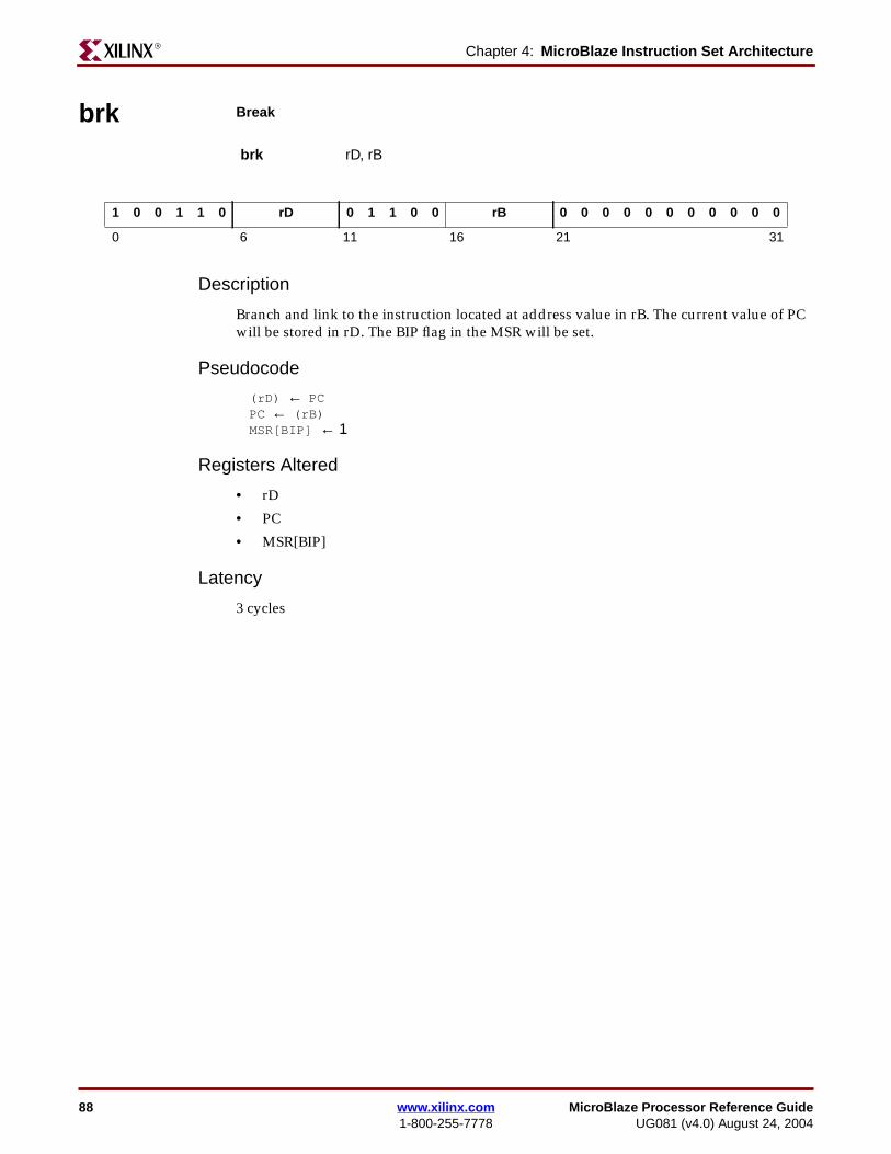
88 www.xilinx.com MicroBlaze Processor Reference Guide1-800-255-7778 UG081 (v4.0) August 24, 2004
Chapter 4: MicroBlaze Instruction Set ArchitectureR
brk Break
Description
Branch and link to the instruction located at address value in rB. The current value of PCwill be stored in rD. The BIP flag in the MSR will be set.
Pseudocode
(rD) ← PCPC ← (rB)MSR[BIP] ← 1
Registers Altered
• rD
• PC
• MSR[BIP]
Latency
3 cycles
brk rD, rB
1 0 0 1 1 0 rD 0 1 1 0 0 rB 0 0 0 0 0 0 0 0 0 0 0
0 6 11 16 21 31

MicroBlaze Processor Reference Guide www.xilinx.com 89UG081 (v4.0) August 24, 2004 1-800-255-7778
InstructionsR
brki Break Immediate
Description
Branch and link to the instruction located at address value in IMM, sign-extended to 32bits. The current value of PC will be stored in rD. The BIP flag in the MSR will be set.
Pseudocode
(rD) ← PCPC ← sext(IMM)MSR[BIP] ← 1
Registers Altered
• rD
• PC
• MSR[BIP]
Latency
3 cycles
Note
By default, Type B Instructions will take the 16-bit IMM field value and sign extend it to 32bits to use as the immediate operand. This behavior can be overridden by preceding theType B instruction with an imm instruction. See the imm instruction for details on using32-bit immediate values.
brki rD, IMM
1 0 1 1 1 0 rD 0 1 1 0 0 IMM
0 6 11 16 31

90 www.xilinx.com MicroBlaze Processor Reference Guide1-800-255-7778 UG081 (v4.0) August 24, 2004
Chapter 4: MicroBlaze Instruction Set ArchitectureR
bs Barrel Shift
Description
Shifts the contents of register rA by the amount specified in register rB and puts the resultin register rD.
The mnemonic bsll sets the S bit (Side bit). If the S bit is set, the barrel shift is done to theleft. The mnemonics bsrl and bsra clear the S bit and the shift is done to the right.
The mnemonic bsra will set the T bit (Type bit). If the T bit is set, the barrel shift performedis Arithmetical. The mnemonics bsrl and bsll clear the T bit and the shift performed isLogical.
Pseudocode
if S = 1 then(rD) ← (rA) << (rB)[27:31]
elseif T = 1 thenif ((rB)[27:31]) ≠ 0 then(rD)[0:(rB)[27:31]-1] ← (rA)[0](rD)[(rB)[27:31]:31] ← (rA) >> (rB)[27:31]
else(rD) ← (rA)
else(rD) ← (rA) >> (rB)[27:31]
Registers Altered
• rD
Latency
2 cycles
Note
These instructions are optional. To use them, MicroBlaze has to be configured to use barrelshift instructions.
bsrl rD, rA, rB Barrel Shift Right Logical
bsra rD, rA, rB Barrel Shift Right Arithmetical
bsll rD, rA, rB Barrel Shift Left Logical
0 1 0 0 0 1 rD rA rB S T 0 0 0 0 0 0 0 0 0
0 6 11 16 21 31

MicroBlaze Processor Reference Guide www.xilinx.com 91UG081 (v4.0) August 24, 2004 1-800-255-7778
InstructionsR
bsi Barrel Shift Immediate
Description
Shifts the contents of register rA by the amount specified by IMM and puts the result inregister rD.
The mnemonic bsll sets the S bit (Side bit). If the S bit is set, the barrel shift is done to theleft. The mnemonics bsrl and bsra clear the S bit and the shift is done to the right.
The mnemonic bsra will set the T bit (Type bit). If the T bit is set, the barrel shift performedis Arithmetical. The mnemonics bsrl and bsll clear the T bit and the shift performed isLogical.
Pseudocode
if S = 1 then(rD) ← (rA) << IMM
elseif T = 1 thenif IMM ≠ 0 then(rD)[0:IMM-1] ← (rA)[0](rD)[IMM:31] ← (rA) >> IMM
else(rD) ← (rA)
else(rD) ← (rA) >> IMM
Registers Altered
• rD
Latency
2 cycles
Notes
These are not Type B Instructions. There is no effect from a preceding imm instruction.
These instructions are optional. To use them, MicroBlaze has to be configured to use barrelshift instructions.
bsrli rD, rA, IMM Barrel Shift Right Logical Immediate
bsrai rD, rA, IMM Barrel Shift Right Arithmetical Immediate
bslli rD, rA, IMM Barrel Shift Left Logical Immediate
0 1 1 0 0 1 rD rA 0 0 0 0 0 S T 0 0 0 0 IMM
0 6 11 16 21 27 31

92 www.xilinx.com MicroBlaze Processor Reference Guide1-800-255-7778 UG081 (v4.0) August 24, 2004
Chapter 4: MicroBlaze Instruction Set ArchitectureR
cmp Integer Compare
Description
The contents of register rA is subtracted from the contents of register rB and the result isplaced into register rD.
The MSB bit of rD is adjusted to shown true relation between rA and rB. If the U bit is set,rA and rB is considered unsigned values. If the U bit is clear, rA and rB is consideredsigned values
.
Pseudocode
(rD) ← (rB) + (rA) + 1(rD)(MSB) ← (rA) > (rB)
Registers Altered
• rD
Latency
1 cycle
.
cmp rD, rA, rB compare rB with rA (signed)
cmpu rD, rA, rB compare rB with rA (unsigned)
0 0 0 1 0 1 rD rA rB 0 0 0 0 0 0 0 0 0 U 0
0 6 11 16 21 31

MicroBlaze Processor Reference Guide www.xilinx.com 93UG081 (v4.0) August 24, 2004 1-800-255-7778
InstructionsR
get get from fsl interface
Description
MicroBlaze will read from the FSLx interface and place the result in register rD.
The get instruction has four variants.
The blocking versions (when ‘n’ bit is ‘0’) will stall microblaze until the data from the FSLinterface is valid. The non-blocking versions will not stall microblaze and will set carry to‘0’ if the data was valid and to ‘1’ if the data was invalid.
The get and nget instructions expect the control bit from the FSL interface to be ‘0’. If thisis not the case, the instruction will set MSR[FSL_Error] to ‘1’. The cget and ncgetinstructions expect the control bit from the FSL interface to be ‘1’. If this is not the case, theinstruction will set MSR[FSL_Error] to ‘1’.
Pseudocode
(rD) ← FSLxif (n = 1) thenMSR[Carry] ← not (FSLx Exists bit)
if ((FSLx Control bit) == c) thenMSR[FSL_Error] ← 0
elseMSR[FSL_Error] ← 1
Registers Altered
• rD
• MSR[FSL_Error]
• MSR[Carry]
Latency
2 cycles if non-blocking or if data is valid at the FSL interface. For blocking instruction,MicroBlaze will stall until the data is valid
Note
For nget and ncget, a rsubc instruction can be used for counting down a index variable
get rD, FSLx get data from FSL x (blocking)
nget rD, FSLx get data from FSL x (non-blocking)
cget rD, FSLx get control from FSL x (blocking)
ncget rD, FSLx get control from FSL x (non-blocking)
0 1 1 0 1 1 rD 0 0 0 0 0 0 n c 0 0 0 0 0 0 0 0 0 0 FSLx
0 6 11 16 29 31

94 www.xilinx.com MicroBlaze Processor Reference Guide1-800-255-7778 UG081 (v4.0) August 24, 2004
Chapter 4: MicroBlaze Instruction Set ArchitectureR
idiv Integer Divide
Description
The contents of register rB is divided by the contents of register rA and the result is placedinto register rD.
If the U bit is set, rA and rB is considered unsigned values. If the U bit is clear, rA and rB isconsidered signed values
If the value of rA is 0, the divide_by_zero bit in MSR will be set and the value in rD will be0.
Pseudocode
if (rA) = 0then(rD) ← 0
else(rD) ← (rB) / (rA)
Registers Altered
• rD
• MSR[Divide_By_Zero]
Latency
2 cycles if (rA) = 0, otherwise 34 cycles
Note
This instruction is only valid if MicroBlaze is configured to use a hardware divider.
idiv rD, rA, rB divide rB by rA (signed)
idivu rD, rA, rB divide rB by rA (unsigned)
0 1 0 0 1 0 rD rA rB 0 0 0 0 0 0 0 0 0 U 0
0 6 11 16 21 31

MicroBlaze Processor Reference Guide www.xilinx.com 95UG081 (v4.0) August 24, 2004 1-800-255-7778
InstructionsR
.imm Immediate
Description
The instruction imm loads the IMM value into a temporary register. It also locks this valueso it can be used by the following instruction and form a 32-bit immediate value.
The instruction imm is used in conjunction with Type B instructions. Since Type Binstructions have only a 16-bit immediate value field, a 32-bit immediate value cannot beused directly. However, 32-bit immediate values can be used in MicroBlaze. By default,Type B Instructions will take the 16-bit IMM field value and sign extend it to 32 bits to useas the immediate operand. This behavior can be overridden by preceding the Type Binstruction with an imm instruction. The imm instruction locks the 16-bit IMM valuetemporarily for the next instruction. A Type B instruction that immediately follows theimm instruction will then form a 32-bit immediate value from the 16-bit IMM value of theimm instruction (upper 16 bits) and its own 16-bit immediate value field (lower 16 bits). Ifno Type B instruction follows the IMM instruction, the locked value gets unlocked andbecomes useless.
Latency
1 cycle
Notes
The imm instruction and the Type B instruction following it are atomic, hence no interruptsare allowed between them.
The assembler provided by Xilinx automatically detects the need for imm instructions.When a 32-bit IMM value is specified in a Type B instruction, the assembler converts theIMM value to a 16-bit one to assemble the instruction and inserts an imm instruction beforeit in the executable file.
imm IMM
1 0 1 1 0 0 0 0 0 0 0 0 0 0 0 0 IMM
0 6 11 16 31

96 www.xilinx.com MicroBlaze Processor Reference Guide1-800-255-7778 UG081 (v4.0) August 24, 2004
Chapter 4: MicroBlaze Instruction Set ArchitectureR
lbu Load Byte Unsigned
Description
Loads a byte (8 bits) from the memory location that results from adding the contents ofregisters rA and rB. The data is placed in the least significant byte of register rD and theother three bytes in rD are cleared.
Pseudocode
Addr ← (rA) + (rB)(rD)[24:31] ← Mem(Addr)(rD)[0:23] ← 0
Registers Altered
• rD
Latency
2 cycles
lbu rD, rA, rB
1 1 0 0 0 0 rD rA rB 0 0 0 0 0 0 0 0 0 0 0
0 6 11 16 21 31

MicroBlaze Processor Reference Guide www.xilinx.com 97UG081 (v4.0) August 24, 2004 1-800-255-7778
InstructionsR
lbui Load Byte Unsigned Immediate
Description
Loads a byte (8 bits) from the memory location that results from adding the contents ofregister rA with the value in IMM, sign-extended to 32 bits. The data is placed in the leastsignificant byte of register rD and the other three bytes in rD are cleared.
Pseudocode
Addr ← (rA) + sext(IMM)(rD)[24:31] ← Mem(Addr)(rD)[0:23] ← 0
Registers Altered
• rD
Latency
2 cycles
Note
By default, Type B Instructions will take the 16-bit IMM field value and sign extend it to 32bits to use as the immediate operand. This behavior can be overridden by preceding theType B instruction with an imm instruction. See the imm instruction for details on using32-bit immediate values.
lbui rD, rA, IMM
1 1 1 0 0 0 rD rA IMM
0 6 11 16 31

98 www.xilinx.com MicroBlaze Processor Reference Guide1-800-255-7778 UG081 (v4.0) August 24, 2004
Chapter 4: MicroBlaze Instruction Set ArchitectureR
lhu Load Halfword Unsigned
Description
Loads a halfword (16 bits) from the halfword aligned memory location that results fromadding the contents of registers rA and rB. The data is placed in the least significanthalfword of register rD and the most significant halfword in rD is cleared.
Pseudocode
Addr ← (rA) + (rB)Addr[31] ← 0(rD)[16:31] ← Mem(Addr)(rD)[0:15] ← 0
Registers Altered
• rD
Latency
2 cycles
lhu rD, rA, rB
1 1 0 0 0 1 rD rA rB 0 0 0 0 0 0 0 0 0 0 0
0 6 11 16 21 31

MicroBlaze Processor Reference Guide www.xilinx.com 99UG081 (v4.0) August 24, 2004 1-800-255-7778
InstructionsR
lhui Load Halfword Unsigned Immediate
Description
Loads a halfword (16 bits) from the halfword aligned memory location that results fromadding the contents of register rA and the value in IMM, sign-extended to 32 bits. The datais placed in the least significant halfword of register rD and the most significant halfwordin rD is cleared.
Pseudocode
Addr ← (rA) + sext(IMM)Addr[31] ← 0(rD)[16:31] ← Mem(Addr)(rD)[0:15] ← 0
Registers Altered
• rD
Latency
2 cycles
Note
By default, Type B Instructions will take the 16-bit IMM field value and sign extend it to 32bits to use as the immediate operand. This behavior can be overridden by preceding theType B instruction with an imm instruction. See the imm instruction for details on using32-bit immediate values.
lhui rD, rA, IMM
1 1 1 0 0 1 rD rA IMM
0 6 11 16 31

100 www.xilinx.com MicroBlaze Processor Reference Guide1-800-255-7778 UG081 (v4.0) August 24, 2004
Chapter 4: MicroBlaze Instruction Set ArchitectureR
lw Load Word
Description
Loads a word (32 bits) from the word aligned memory location that results from addingthe contents of registers rA and rB. The data is placed in register rD.
Pseudocode
Addr ← (rA) + (rB)Addr[30:31] ← 00(rD) ← Mem(Addr)
Registers Altered
• rD
Latency
2 cycles
lw rD, rA, rB
1 1 0 0 1 0 rD rA rB 0 0 0 0 0 0 0 0 0 0 0
0 6 11 16 21 31

MicroBlaze Processor Reference Guide www.xilinx.com 101UG081 (v4.0) August 24, 2004 1-800-255-7778
InstructionsR
lwi Load Word Immediate
Description
Loads a word (32 bits) from the word aligned memory location that results from addingthe contents of register rA and the value IMM, sign-extended to 32 bits. The data is placedin register rD.
Pseudocode
Addr ← (rA) + sext(IMM)Addr[30:31] ← 00(rD) ← Mem(Addr)
Registers Altered
• rD
Latency
2 cycles
Note
By default, Type B Instructions will take the 16-bit IMM field value and sign extend it to 32bits to use as the immediate operand. This behavior can be overridden by preceding theType B instruction with an imm instruction. See the imm instruction for details on using32-bit immediate values.
lwi rD, rA, IMM
1 1 1 0 1 0 rD rA IMM
0 6 11 16 31

102 www.xilinx.com MicroBlaze Processor Reference Guide1-800-255-7778 UG081 (v4.0) August 24, 2004
Chapter 4: MicroBlaze Instruction Set ArchitectureR
mfs Move From Special Purpose Register
Description
Copies the contents of the special purpose register rS into register rD.
Pseudocode
(rD) ← (rS)
Registers Altered
• rD
Latency
1 cycle
Note
To refer to special purpose registers in assembly language, use rpc for PC, rmsr for MSR,rear for EAR, and resr for ESR. Source registers EAR and ESR are only valid in MicroBlazev3.00a and higher.
mfs rD, rS
1 0 0 1 0 1 rD 0 0 0 0 0 1 0 0 0 0 0 0 0 0 0 0 0 0 0 0 rS
0 6 11 16 31

MicroBlaze Processor Reference Guide www.xilinx.com 103UG081 (v4.0) August 24, 2004 1-800-255-7778
InstructionsR
msrclr Read MSR and clear bits in MSR
Description
Copies the contents of the special purpose register MSR into register rD.Bit positions in the IMM value that are 1 are cleared in the MSR. Bit positions that are 0 inthe IMM value are left untouched.
Pseudocode
(rD) ← (MSR)(MSR) ← (MSR) ∧ ( IMM))
Registers Altered
• rD
• MSR
Latency
1 cycle
Note
This instruction is only valid if C_USE_MSR_INSTR is set for MicroBlaze.
The immediate values has to be less than 2^14. Only bits 18 to 31 of the MSR can be cleared.
This instruction only exists in version 2.10.a and above.
msrclr rD, Imm
1 0 0 1 0 1 rD 0 0 0 0 1 0 0 Imm14
0 6 11 16 17 18 31

104 www.xilinx.com MicroBlaze Processor Reference Guide1-800-255-7778 UG081 (v4.0) August 24, 2004
Chapter 4: MicroBlaze Instruction Set ArchitectureR
msrset Read MSR and set bits in MSR
Description
Copies the contents of the special purpose register MSR into register rD.Bit positions in the IMM value that are 1 are set in the MSR. Bit positions that are 0 in theIMM value are left untouched.
Pseudocode
(rD) ← (MSR)(MSR) ← (MSR) ∨ (IMM)
Registers Altered
• rD
• MSR
Latency
1 cycle
Note
This instruction is only valid if C_USE_MSR_INSTR is set for MicroBlaze.
The immediate values has to be less than 2^14. Only bits 18 to 31 of the MSR can be set.
This instruction only exists in version 2.10.a and above.
msrset rD, Imm
1 0 0 1 0 1 rD 0 0 0 0 0 0 0 Imm14
0 6 11 16 18 31

MicroBlaze Processor Reference Guide www.xilinx.com 105UG081 (v4.0) August 24, 2004 1-800-255-7778
InstructionsR
mts Move To Special Purpose Register
Description
Copies the contents of register rD into the MSR register.
Pseudocode
(rS) ← (rA)
Registers Altered
• rS
Latency
1 cycle
Notes
You cannot write to the PC using the MTS instruction.
When writing to MSR using MTS, the value written will take effect one clock cycle afterexecuting the MTS instruction.
To refer to special purpose registers in assembly language, use rmsr for MSR. PC, ESR andEAR can not be written by the MTS instruction.
mts rS, rA
1 0 0 1 0 1 0 0 0 0 0 rA 1 1 0 0 0 0 0 0 0 0 0 0 0 0 0 rS
0 6 11 16 31

106 www.xilinx.com MicroBlaze Processor Reference Guide1-800-255-7778 UG081 (v4.0) August 24, 2004
Chapter 4: MicroBlaze Instruction Set ArchitectureR
mul Multiply
Description
Multiplies the contents of registers rA and rB and puts the result in register rD. This is a 32-bit by 32-bit multiplication that will produce a 64-bit result. The least significant word ofthis value is placed in rD. The most significant word is discarded.
Pseudocode
(rD) ← LSW( (rA) × (rB) )
Registers Altered
• rD
Latency
3 cycles
Note
This instruction is only valid if the target architecture has an embedded multiplier.
mul rD, rA, rB
0 1 0 0 0 0 rD rA rB 0 0 0 0 0 0 0 0 0 0 0
0 6 11 16 21 31

MicroBlaze Processor Reference Guide www.xilinx.com 107UG081 (v4.0) August 24, 2004 1-800-255-7778
InstructionsR
muli Multiply Immediate
Description
Multiplies the contents of registers rA and the value IMM, sign-extended to 32 bits; andputs the result in register rD. This is a 32-bit by 32-bit multiplication that will produce a 64-bit result. The least significant word of this value is placed in rD. The most significant wordis discarded.
Pseudocode
(rD) ← LSW( (rA) × sext(IMM) )
Registers Altered
• rD
Latency
3 cycles
Notes
By default, Type B Instructions will take the 16-bit IMM field value and sign extend it to 32bits to use as the immediate operand. This behavior can be overridden by preceding theType B instruction with an imm instruction. See the imm instruction for details on using32-bit immediate values.
This instruction is only valid if the target architecture has an embedded multiplier.
muli rD, rA, IMM
0 1 1 0 0 0 rD rA IMM
0 6 11 16 31

108 www.xilinx.com MicroBlaze Processor Reference Guide1-800-255-7778 UG081 (v4.0) August 24, 2004
Chapter 4: MicroBlaze Instruction Set ArchitectureR
or Logical OR
Description
The contents of register rA are ORed with the contents of register rB; the result is placedinto register rD.
Pseudocode
(rD) ← (rA) ∨ (rB)
Registers Altered
• rD
Latency
1 cycle
or rD, rA, rB
1 0 0 0 0 0 rD rA rB 0 0 0 0 0 0 0 0 0 0 0
0 6 11 16 21 31

MicroBlaze Processor Reference Guide www.xilinx.com 109UG081 (v4.0) August 24, 2004 1-800-255-7778
InstructionsR
ori Logical OR with Immediate
Description
The contents of register rA are ORed with the extended IMM field, sign-extended to 32bits; the result is placed into register rD.
Pseudocode
(rD) ← (rA) ∨ (IMM)
Registers Altered
• rD
Latency
1 cycle
Note
By default, Type B Instructions will take the 16-bit IMM field value and sign extend it to 32bits to use as the immediate operand. This behavior can be overridden by preceding theType B instruction with an imm instruction. See the imm instruction for details on using32-bit immediate values.
ori rD, rA, IMM
1 0 1 0 0 0 rD rA IMM
0 6 11 16 31

110 www.xilinx.com MicroBlaze Processor Reference Guide1-800-255-7778 UG081 (v4.0) August 24, 2004
Chapter 4: MicroBlaze Instruction Set ArchitectureR
put put to fsl interface
Description
MicroBlaze will write the value from register rA to the FSLx interface.
The put instruction has four variants.
The blocking versions (when ‘n’ is ‘0’) will stall microblaze until there is space available inthe FSL interface. The non-blocking versions will not stall microblaze and will set carry to‘0’ if space was available and to ‘1’ if no space was available.
The put and nput instructions will set the control bit to the FSL interface to ‘0’ and the cputand ncput instruction will set the control bit to ‘1’.
Pseudocode
(FSLx) ← (rA)if (n = 1) thenMSR[Carry] ← (FSLx Full bit)
(FSLx Control bit) ← C
Registers Altered
• MSR[Carry]
Latency
2 cycles for non-blocking or if space is available on the FSL interface. For blocking,MicroBlaze stalls until space is available on the FSL interface.
put rA, FSLx put data to FSL x (blocking)
nput rA, FSLx put data to FSL x (non-blocking)
cput rA, FSLx put control to FSL x (blocking)
ncput rA, FSLx put control to FSL x (non-blocking)
0 1 1 0 1 1 0 0 0 0 0 rA 1 n c 0 0 0 0 0 0 0 0 0 0 FSLx
0 6 11 16 29 31

MicroBlaze Processor Reference Guide www.xilinx.com 111UG081 (v4.0) August 24, 2004 1-800-255-7778
InstructionsR
rsub Arithmetic Reverse Subtract
Description
The contents of register rA is subtracted from the contents of register rB and the result isplaced into register rD. Bit 3 of the instruction (labeled as K in the figure) is set to a one forthe mnemonic rsubk. Bit 4 of the instruction (labeled as C in the figure) is set to a one forthe mnemonic rsubc. Both bits are set to a one for the mnemonic rsubkc.
When an rsub instruction has bit 3 set (rsubk, rsubkc), the carry flag will Keep its previousvalue regardless of the outcome of the execution of the instruction. If bit 3 is cleared (rsub,rsubc), then the carry flag will be affected by the execution of the instruction.
When bit 4 of the instruction is set to a one (rsubc, rsubkc), the content of the carry flag(MSR[C]) affects the execution of the instruction. When bit 4 is cleared (rsub, rsubk), thecontent of the carry flag does not affect the execution of the instruction (providing a normalsubtraction).
Pseudocode
if C = 0 then(rD) ← (rB) + (rA) + 1
else(rD) ← (rB) + (rA) + MSR[C]
if K = 0 thenMSR[C] ← CarryOut
Registers Altered
• rD
• MSR[C]
Latency
1 cycle
Notes
In subtractions, Carry = (Borrow). When the Carry is set by a subtraction, it means thatthere is no Borrow, and when the Carry is cleared, it means that there is a Borrow.
rsub rD, rA, rB Subtract
rsubc rD, rA, rB Subtract with Carry
rsubk rD, rA, rB Subtract and Keep Carry
rsubkc rD, rA, rB Subtract with Carry and Keep Carry
0 0 0 K C 1 rD rA rB 0 0 0 0 0 0 0 0 0 0 0
0 6 11 16 21 31

112 www.xilinx.com MicroBlaze Processor Reference Guide1-800-255-7778 UG081 (v4.0) August 24, 2004
Chapter 4: MicroBlaze Instruction Set ArchitectureR
rsubi Arithmetic Reverse Subtract Immediate
Description
The contents of register rA is subtracted from the value of IMM, sign-extended to 32 bits,and the result is placed into register rD. Bit 3 of the instruction (labeled as K in the figure)is set to a one for the mnemonic rsubik. Bit 4 of the instruction (labeled as C in the figure)is set to a one for the mnemonic rsubic. Both bits are set to a one for the mnemonic rsubikc.
When an rsubi instruction has bit 3 set (rsubik, rsubikc), the carry flag will Keep itsprevious value regardless of the outcome of the execution of the instruction. If bit 3 iscleared (rsubi, rsubic), then the carry flag will be affected by the execution of theinstruction. When bit 4 of the instruction is set to a one (rsubic, rsubikc), the content of thecarry flag (MSR[C]) affects the execution of the instruction. When bit 4 is cleared (rsubi,rsubik), the content of the carry flag does not affect the execution of the instruction(providing a normal subtraction).
Pseudocode
if C = 0 then(rD) ← sext(IMM) + (rA) + 1
else(rD) ← sext(IMM) + (rA) + MSR[C]
if K = 0 thenMSR[C] ← CarryOut
Registers Altered
• rD
• MSR[C]
Latency
1 cycle
Notes
In subtractions, Carry = (Borrow). When the Carry is set by a subtraction, it means thatthere is no Borrow, and when the Carry is cleared, it means that there is a Borrow.
By default, Type B Instructions will take the 16-bit IMM field value and sign extend it to 32bits to use as the immediate operand. This behavior can be overridden by preceding theType B instruction with an imm instruction. See the imm instruction for details on using32-bit immediate values.
rsubi rD, rA, IMM Subtract Immediate
rsubic rD, rA, IMM Subtract Immediate with Carry
rsubik rD, rA, IMM Subtract Immediate and Keep Carry
rsubikc rD, rA, IMM Subtract Immediate with Carry and Keep Carry
0 0 1 K C 1 rD rA IMM
0 6 11 16 31

MicroBlaze Processor Reference Guide www.xilinx.com 113UG081 (v4.0) August 24, 2004 1-800-255-7778
InstructionsR
rtbd Return from Breakrn from Interrupt
Description
Return from break will branch to the location specified by the contents of rA plus the IMMfield, sign-extended to 32 bits. It will also enable breaks after execution by clearing the BIPflag in the MSR.
This instruction always has a delay slot. The instruction following the RTBD is alwaysexecuted before the branch target. That delay slot instruction has breaks disabled.
Pseudocode
PC ← (rA) + sext(IMM)allow following instruction to complete executionMSR[BIP] ← 0
Registers Altered
• PC
• MSR[BIP]
Latency
2 cycles
rtbd rA, IMM
1 0 1 1 0 1 1 0 0 1 0 rA IMM
0 6 11 16 31

114 www.xilinx.com MicroBlaze Processor Reference Guide1-800-255-7778 UG081 (v4.0) August 24, 2004
Chapter 4: MicroBlaze Instruction Set ArchitectureR
rtid Return from Interruptrn from Interrupt
Description
Return from interrupt will branch to the location specified by the contents of rA plus theIMM field, sign-extended to 32 bits. It will also enable interrupts after execution.
This instruction always has a delay slot. The instruction following the RTID is alwaysexecuted before the branch target. That delay slot instruction has interrupts disabled.
Pseudocode
PC ← (rA) + sext(IMM)allow following instruction to complete executionMSR[IE] ← 1
Registers Altered
• PC
• MSR[IE]
Latency
2 cycles
rtid rA, IMM
1 0 1 1 0 1 1 0 0 0 1 rA IMM
0 6 11 16 31

MicroBlaze Processor Reference Guide www.xilinx.com 115UG081 (v4.0) August 24, 2004 1-800-255-7778
InstructionsR
rted Return from Exception
Description
Return from exception will branch to the location specified by the contents of rA plus theIMM field, sign-extended to 32 bits. The instruction will also enable exceptions afterexecution.
This instruction always has a delay slot. The instruction following the RTED is alwaysexecuted before the branch target.
Pseudocode
PC ← (rA) + sext(IMM)allow following instruction to complete executionMSR[EE] ← 1MSR[EIP] ← 0ESR ← 0
Registers Altered
• PC
• MSR[EE]
• MSR[EIP]
• ESR
Latency
2 cycles
Notes
This instruction is only available in MicroBlaze v3.00a or higher.
rtsd rA, IMM
1 0 1 1 0 1 1 0 0 1 0 rA IMM
0 6 11 16 31

116 www.xilinx.com MicroBlaze Processor Reference Guide1-800-255-7778 UG081 (v4.0) August 24, 2004
Chapter 4: MicroBlaze Instruction Set ArchitectureR
rtsd Return from Subroutine
Description
Return from subroutine will branch to the location specified by the contents of rA plus theIMM field, sign-extended to 32 bits.
This instruction always has a delay slot. The instruction following the RTSD is alwaysexecuted before the branch target.
Pseudocode
PC ← (rA) + sext(IMM)allow following instruction to complete execution
Registers Altered
• PC
Latency
2 cycles
rtsd rA, IMM
1 0 1 1 0 1 1 0 0 0 0 rA IMM
0 6 11 16 31

MicroBlaze Processor Reference Guide www.xilinx.com 117UG081 (v4.0) August 24, 2004 1-800-255-7778
InstructionsR
sb Store Byte
Description
Stores the contents of the least significant byte of register rD, into the memory location thatresults from adding the contents of registers rA and rB.
Pseudocode
Addr ← (rA) + (rB)Mem(Addr) ← (rD)[24:31]
Registers Altered
• None
Latency
2 cycles
sb rD, rA, rB
1 1 0 1 0 0 rD rA rB 0 0 0 0 0 0 0 0 0 0 0
0 6 11 16 21 31

118 www.xilinx.com MicroBlaze Processor Reference Guide1-800-255-7778 UG081 (v4.0) August 24, 2004
Chapter 4: MicroBlaze Instruction Set ArchitectureR
sbi Store Byte Immediate
Description
Stores the contents of the least significant byte of register rD, into the memory location thatresults from adding the contents of register rA and the value IMM, sign-extended to 32bits.
Pseudocode
Addr ← (rA) + sext(IMM)Mem(Addr) ← (rD)[24:31]
Registers Altered
• None
Latency
2 cycles
Note
By default, Type B Instructions will take the 16-bit IMM field value and sign extend it to 32bits to use as the immediate operand. This behavior can be overridden by preceding theType B instruction with an imm instruction. See the imm instruction for details on using32-bit immediate values.
sbi rD, rA, IMM
1 1 1 1 0 0 rD rA IMM
0 6 11 16 31
MicroBlaze Processor Reference Guide www.xilinx.com 119UG081 (v4.0) August 24, 2004 1-800-255-7778
InstructionsR
sext16 Sign Extend Halfword
Description
This instruction sign-extends a halfword (16 bits) into a word (32 bits). Bit 16 in rA will becopied into bits 0-15 of rD. Bits 16-31 in rA will be copied into bits 16-31 of rD.
Pseudocode
(rD)[0:15] ← (rA)[16](rD)[16:31] ← (rA)[16:31]
Registers Altered
• rD
Latency
1 cycle
sext16 rD, rA
1 0 0 1 0 0 rD rA 0 0 0 0 0 0 0 0 0 1 1 0 0 0 0 1
0 6 11 16 31

120 www.xilinx.com MicroBlaze Processor Reference Guide1-800-255-7778 UG081 (v4.0) August 24, 2004
Chapter 4: MicroBlaze Instruction Set ArchitectureR
sext8 Sign Extend Byte
Description
This instruction sign-extends a byte (8 bits) into a word (32 bits). Bit 24 in rA will be copiedinto bits 0-23 of rD. Bits 24-31 in rA will be copied into bits 24-31 of rD.
Pseudocode
(rD)[0:23] ← (rA)[24](rD)[24:31] ← (rA)[24:31]
Registers Altered
• rD
Latency
1 cycle
sext8 rD, rA
1 0 0 1 0 0 rD rA 0 0 0 0 0 0 0 0 0 1 1 0 0 0 0 0
0 6 11 16 31

MicroBlaze Processor Reference Guide www.xilinx.com 121UG081 (v4.0) August 24, 2004 1-800-255-7778
InstructionsR
sh Store Halfword
Description
Stores the contents of the least significant halfword of register rD, into the halfwordaligned memory location that results from adding the contents of registers rA and rB.
Pseudocode
Addr ← (rA) + (rB)Addr[31] ← 0Mem(Addr) ← (rD)[16:31]
Registers Altered
• None
Latency
2 cycles
sh rD, rA, rB
1 1 0 1 0 1 rD rA rB 0 0 0 0 0 0 0 0 0 0 0
0 6 11 16 21 31

122 www.xilinx.com MicroBlaze Processor Reference Guide1-800-255-7778 UG081 (v4.0) August 24, 2004
Chapter 4: MicroBlaze Instruction Set ArchitectureR
shi Store Halfword Immediate
Description
Stores the contents of the least significant halfword of register rD, into the halfwordaligned memory location that results from adding the contents of register rA and the valueIMM, sign-extended to 32 bits.
Pseudocode
Addr ← (rA) + sext(IMM)Addr[31] ← 0Mem(Addr) ← (rD)[16:31]
Registers Altered
• None
Latency
2 cycles
Note
By default, Type B Instructions will take the 16-bit IMM field value and sign extend it to 32bits to use as the immediate operand. This behavior can be overridden by preceding theType B instruction with an imm instruction. See the imm instruction for details on using32-bit immediate values.
shi rD, rA, IMM
1 1 1 1 0 1 rD rA IMM
0 6 11 16 31

MicroBlaze Processor Reference Guide www.xilinx.com 123UG081 (v4.0) August 24, 2004 1-800-255-7778
InstructionsR
sra Shift Right Arithmetic
Description
Shifts arithmetically the contents of register rA, one bit to the right, and places the result inrD. The most significant bit of rA (i.e. the sign bit) placed in the most significant bit of rD.The least significant bit coming out of the shift chain is placed in the Carry flag.
Pseudocode
(rD)[0] ← (rA)[0](rD)[1:31] ← (rA)[0:30]MSR[C] ← (rA)[31]
Registers Altered
• rD
• MSR[C]
Latency
1 cycle
sra rD, rA
1 0 0 1 0 0 rD rA 0 0 0 0 0 0 0 0 0 0 0 0 0 0 0 1
0 6 11 16 31

124 www.xilinx.com MicroBlaze Processor Reference Guide1-800-255-7778 UG081 (v4.0) August 24, 2004
Chapter 4: MicroBlaze Instruction Set ArchitectureR
src Shift Right with Carry
Description
Shifts the contents of register rA, one bit to the right, and places the result in rD. The Carryflag is shifted in the shift chain and placed in the most significant bit of rD. The leastsignificant bit coming out of the shift chain is placed in the Carry flag.
Pseudocode
(rD)[0] ← MSR[C](rD)[1:31] ← (rA)[0:30]MSR[C] ← (rA)[31]
Registers Altered
• rD
• MSR[C]
Latency
1 cycle
src rD, rA
1 0 0 1 0 0 rD rA 0 0 0 0 0 0 0 0 0 0 1 0 0 0 0 1
0 6 11 16 31

MicroBlaze Processor Reference Guide www.xilinx.com 125UG081 (v4.0) August 24, 2004 1-800-255-7778
InstructionsR
srl Shift Right Logical
Description
Shifts logically the contents of register rA, one bit to the right, and places the result in rD.A zero is shifted in the shift chain and placed in the most significant bit of rD. The leastsignificant bit coming out of the shift chain is placed in the Carry flag.
Pseudocode
(rD)[0] ← 0(rD)[1:31] ← (rA)[0:30]MSR[C] ← (rA)[31]
Registers Altered
• rD
• MSR[C]
Latency
1 cycle
srl rD, rA
1 0 0 1 0 0 rD rA 0 0 0 0 0 0 0 0 0 1 0 0 0 0 0 1
0 6 11 16 31

126 www.xilinx.com MicroBlaze Processor Reference Guide1-800-255-7778 UG081 (v4.0) August 24, 2004
Chapter 4: MicroBlaze Instruction Set ArchitectureR
sw Store Word
Description
Stores the contents of register rD, into the word aligned memory location that results fromadding the contents of registers rA and rB.
Pseudocode
Addr ← (rA) + (rB)Addr[30:31] ← 00Mem(Addr) ← (rD)[0:31]
Registers Altered
• None
Latency
2 cycles
sw rD, rA, rB
1 1 0 1 1 0 rD rA rB 0 0 0 0 0 0 0 0 0 0 0
0 6 11 16 21 31

MicroBlaze Processor Reference Guide www.xilinx.com 127UG081 (v4.0) August 24, 2004 1-800-255-7778
InstructionsR
swi Store Word Immediate
Description
Stores the contents of register rD, into the word aligned memory location that results fromadding the contents of registers rA and the value IMM, sign-extended to 32 bits.
Pseudocode
Addr ← (rA) + sext(IMM)Addr[30:31] ← 00Mem(Addr) ← (rD)[0:31]
Register Altered
• None
Latency
2 cycles
Note
By default, Type B Instructions will take the 16-bit IMM field value and sign extend it to 32bits to use as the immediate operand. This behavior can be overridden by preceding theType B instruction with an imm instruction. See the imm instruction for details on using32-bit immediate values.
swi rD, rA, IMM
1 1 1 1 1 0 rD rA IMM
0 6 11 16 31

128 www.xilinx.com MicroBlaze Processor Reference Guide1-800-255-7778 UG081 (v4.0) August 24, 2004
Chapter 4: MicroBlaze Instruction Set ArchitectureR
wdc Write to Data Cache
Description
Write into the data cache tag and data memory. Register rB contains the new data. RegisterrA contains the data address. Bit 30 in rA is the new valid bit and bit 31 is the new lock bit.
The instruction only works when the data cache has been disabled by clearing the Datacache enable bit in the MSR register
Pseudocode
(DCache Tag) ← (rA)(DCache Data) ← (rB)
Registers Altered
• None
Latency
1 cycle
wdc rA,rB
1 0 0 1 0 0 rA rA rB 0 0 0 0 1 1 0 0 1 0 0
0 6 11 16 31

MicroBlaze Processor Reference Guide www.xilinx.com 129UG081 (v4.0) August 24, 2004 1-800-255-7778
InstructionsR
wic Write to Instruction Cache
Description
Write into the instruction cache tag and data memory. Register rB contains the newinstruction data. Register rA contains the instruction address. Bit 30 in rA is the new validbit and bit 31 is the new lock bit.
The instruction only works when the instruction cache has been disabled by clearing theInstruction cache enable bit in the MSR register
Pseudocode
(ICache Tag) ← (rA)(ICache Data) ← (rB)
Registers Altered
• None
Latency
1 cycle
wic rA,rB
1 0 0 1 0 0 rA rA rB 0 0 0 0 1 1 0 1 0 0 0
0 6 11 16 31

130 www.xilinx.com MicroBlaze Processor Reference Guide1-800-255-7778 UG081 (v4.0) August 24, 2004
Chapter 4: MicroBlaze Instruction Set ArchitectureR
xor Logical Exclusive OR
Description
The contents of register rA are XORed with the contents of register rB; the result is placedinto register rD.
Pseudocode
(rD) ← (rA) ⊕ (rB)
Registers Altered
• rD
Latency
1 cycle
xor rD, rA, rB
1 0 0 0 1 0 rD rA rB 0 0 0 0 0 0 0 0 0 0 0
0 6 11 16 21 31
MicroBlaze Processor Reference Guide www.xilinx.com 131UG081 (v4.0) August 24, 2004 1-800-255-7778
InstructionsR
xori Logical Exclusive OR with Immediate
Description
The IMM field is extended to 32 bits by concatenating 16 0-bits on the left. The contents ofregister rA are XORed with the extended IMM field; the result is placed into register rD.
Pseudocode
(rD) ← (rA) ⊕ sext(IMM)
Registers Altered
• rD
Latency
1 cycle
Note
By default, Type B Instructions will take the 16-bit IMM field value and sign extend it to 32bits to use as the immediate operand. This behavior can be overridden by preceding theType B instruction with an imm instruction. See the imm instruction for details on using32-bit immediate values.
xori rA, rD, IMM
1 0 1 0 1 0 rD rA IMM
0 6 11 16 31

132 www.xilinx.com MicroBlaze Processor Reference Guide1-800-255-7778 UG081 (v4.0) August 24, 2004
Chapter 4: MicroBlaze Instruction Set ArchitectureR