Embed Size (px)
Citation preview
Method to Evaluate Cable Discharge Event (CDE)Reliability of Integrated Circuits in CMOS Technology
Tai-Xiang Lai and Ming-Dou Ker Nanoelectronics and Gigascale Systems Laboratory
Institute of Electronics, National Chiao-Tung University, Hsinchu, Taiwan E-mail:[email protected]
Abstract
Cable Discharge Event (CDE) has been the main cause which damages the Ethernet interface in field applications. The transmission line pulsing (TLP) system has been the most popular method to observe electric characteristics of the device under human-body-model (HBM) electrostatic discharge (ESD) stress. In this work, the long-pulse transmission line pulsing (LP-TLP) system is proposed to simulate CDE reliability of the Ethernet integrated circuits, and the results are compared with the conventional 100-ns TLP system. The experimental results have shown that the CDE robustness of NMOS device in a 0.25- m CMOS technology is worse than its HBM ESD robustness.
1. Introduction
Cable Discharge Event (CDE) is a critical reliability issue that requires recognition at all levels in the networking industry. The characteristics of twisted-pair cable in different environments play an important role in CDE event. Frequently changing cable environments also increase the challenge of preventing CDE event. With more understanding on CDE characteristics and discharge waveforms, the designers can achieve the best protection against CDE event through a good chip layout skill and a careful selection of on-chip protection components.
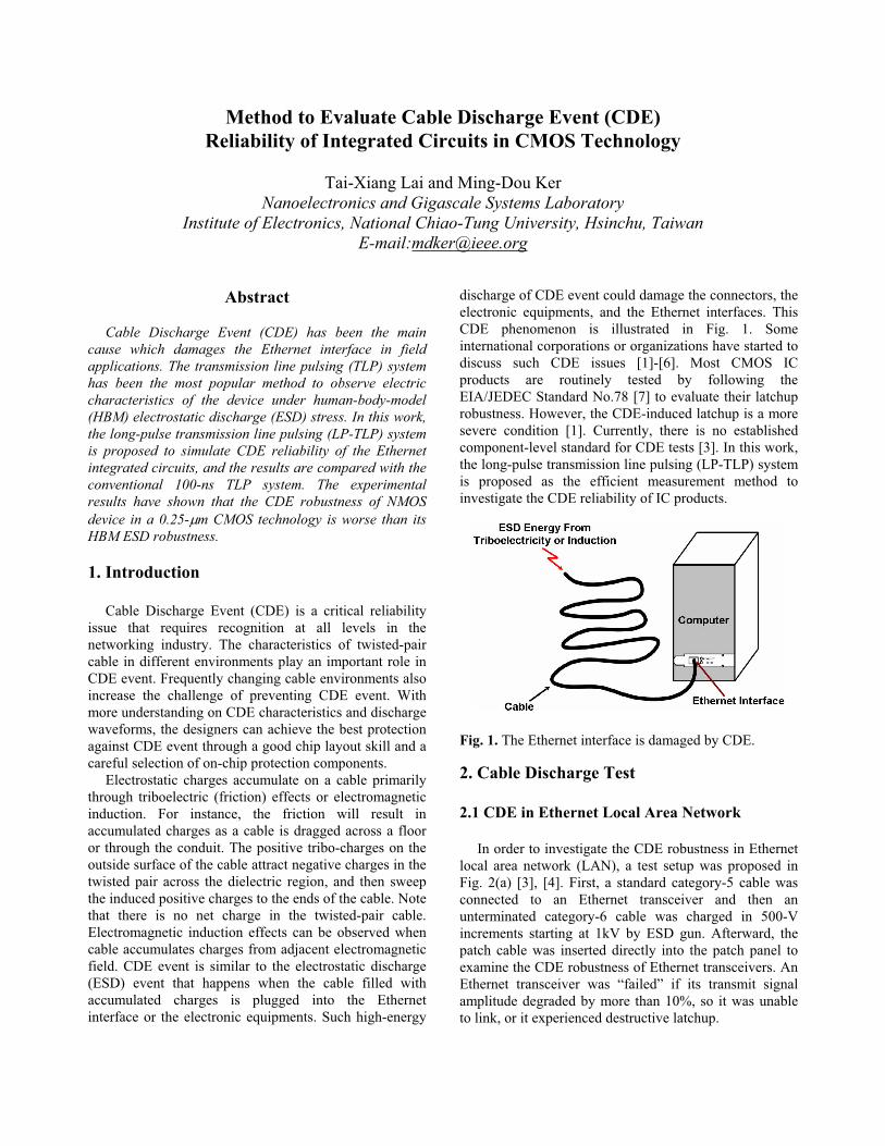
Electrostatic charges accumulate on a cable primarily through triboelectric (friction) effects or electromagnetic induction. For instance, the friction will result in accumulated charges as a cable is dragged across a floor or through the conduit. The positive tribo-charges on the outside surface of the cable attract negative charges in the twisted pair across the dielectric region, and then sweep the induced positive charges to the ends of the cable. Note that there is no net charge in the twisted-pair cable. Electromagnetic induction effects can be observed when cable accumulates charges from adjacent electromagnetic field. CDE event is similar to the electrostatic discharge (ESD) event that happens when the cable filled with accumulated charges is plugged into the Ethernet interface or the electronic equipments. Such high-energy
discharge of CDE event could damage the connectors, the electronic equipments, and the Ethernet interfaces. This CDE phenomenon is illustrated in Fig. 1. Some international corporations or organizations have started to discuss such CDE issues [1]-[6]. Most CMOS IC products are routinely tested by following the EIA/JEDEC Standard No.78 [7] to evaluate their latchup robustness. However, the CDE-induced latchup is a more severe condition [1]. Currently, there is no established component-level standard for CDE tests [3]. In this work, the long-pulse transmission line pulsing (LP-TLP) system is proposed as the efficient measurement method to investigate the CDE reliability of IC products.
Fig. 1. The Ethernet interface is damaged by CDE.
2. Cable Discharge Test
2.1 CDE in Ethernet Local Area Network
In order to investigate the CDE robustness in Ethernet local area network (LAN), a test setup was proposed in Fig. 2(a) [3], [4]. First, a standard category-5 cable was connected to an Ethernet transceiver and then an unterminated category-6 cable was charged in 500-V increments starting at 1kV by ESD gun. Afterward, the patch cable was inserted directly into the patch panel to examine the CDE robustness of Ethernet transceivers. An Ethernet transceiver was “failed” if its transmit signal amplitude degraded by more than 10%, so it was unable to link, or it experienced destructive latchup.
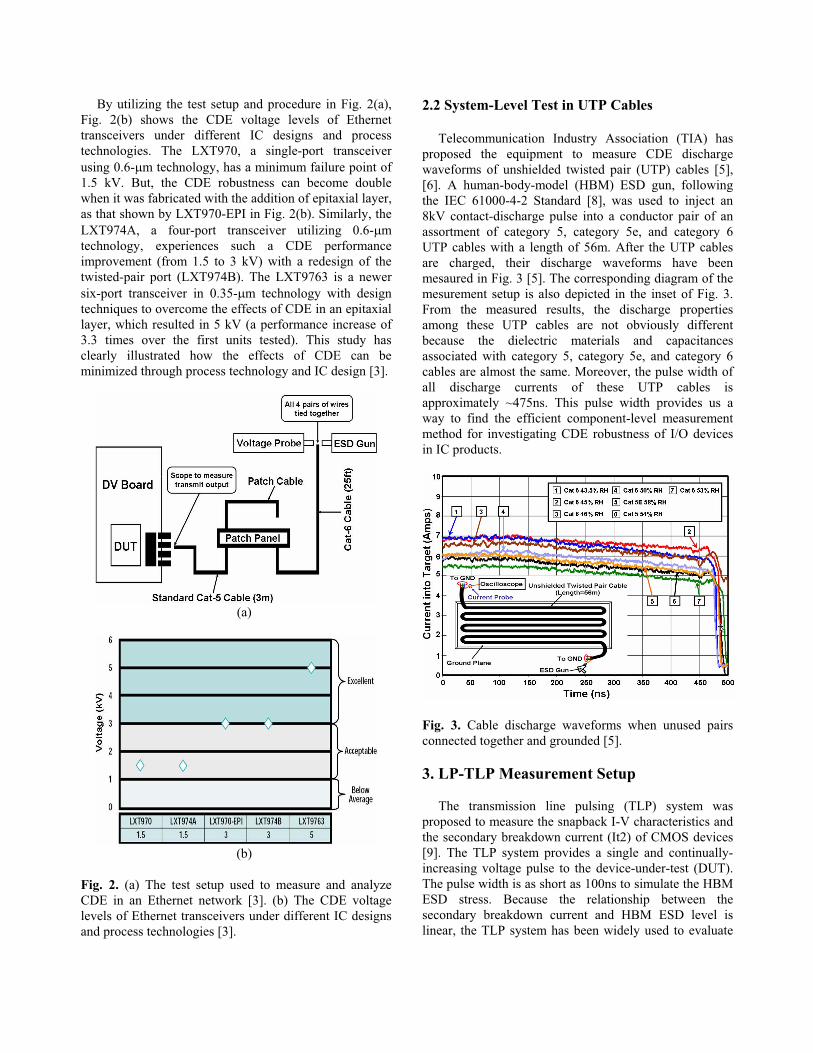
By utilizing the test setup and procedure in Fig. 2(a), Fig. 2(b) shows the CDE voltage levels of Ethernet transceivers under different IC designs and process technologies. The LXT970, a single-port transceiver using 0.6- m technology, has a minimum failure point of 1.5 kV. But, the CDE robustness can become double when it was fabricated with the addition of epitaxial layer, as that shown by LXT970-EPI in Fig. 2(b). Similarly, the LXT974A, a four-port transceiver utilizing 0.6- mtechnology, experiences such a CDE performance improvement (from 1.5 to 3 kV) with a redesign of the twisted-pair port (LXT974B). The LXT9763 is a newer six-port transceiver in 0.35- m technology with design techniques to overcome the effects of CDE in an epitaxial layer, which resulted in 5 kV (a performance increase of 3.3 times over the first units tested). This study has clearly illustrated how the effects of CDE can be minimized through process technology and IC design [3].
(a)
(b)
Fig. 2. (a) The test setup used to measure and analyze CDE in an Ethernet network [3]. (b) The CDE voltage levels of Ethernet transceivers under different IC designs and process technologies [3].
2.2 System-Level Test in UTP Cables
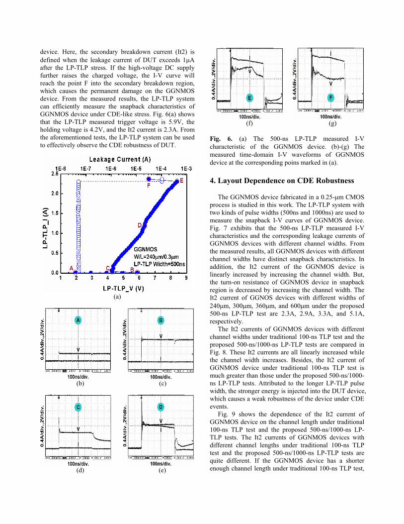
Telecommunication Industry Association (TIA) has proposed the equipment to measure CDE discharge waveforms of unshielded twisted pair (UTP) cables [5], [6]. A human-body-model (HBM) ESD gun, following the IEC 61000-4-2 Standard [8], was used to inject an 8kV contact-discharge pulse into a conductor pair of an assortment of category 5, category 5e, and category 6 UTP cables with a length of 56m. After the UTP cables are charged, their discharge waveforms have been mesaured in Fig. 3 [5]. The corresponding diagram of the mesurement setup is also depicted in the inset of Fig. 3. From the measured results, the discharge properties among these UTP cables are not obviously different because the dielectric materials and capacitances associated with category 5, category 5e, and category 6 cables are almost the same. Moreover, the pulse width of all discharge currents of these UTP cables is approximately ~475ns. This pulse width provides us a way to find the efficient component-level measurement method for investigating CDE robustness of I/O devices in IC products.
Fig. 3. Cable discharge waveforms when unused pairs connected together and grounded [5].
3. LP-TLP Measurement Setup
The transmission line pulsing (TLP) system was proposed to measure the snapback I-V characteristics and the secondary breakdown current (It2) of CMOS devices [9]. The TLP system provides a single and continually- increasing voltage pulse to the device-under-test (DUT). The pulse width is as short as 100ns to simulate the HBM ESD stress. Because the relationship between the secondary breakdown current and HBM ESD level is linear, the TLP system has been widely used to evaluate

the component-level HBM ESD robustness of CMOS devices [10], [11].
By using the characteristics of TLP system, long-pulse transmission line pulsing (LP-TLP) system is proposed in this work. The proposed LP-TLP system with two kinds of long pulse widths (500ns/1000ns) are evidently different from the traditional TLP system with a short pulse width of 100ns. The LP-TLP system with a pulse width of 500ns is consistent to the pulse width (~475ns) of CDE in Fig. 3. Therefore, the LP-TLP system can be utilized to examine the damage situation on the DUT under CDE stress. Fig. 4 sketches the measurement setup for the proposed LP-TLP test. The measurement setup includes a diode, a load resistance (RL), a 50-m transmission line (or a 100-m transmission line), two switches (SW1 and SW2), a high-voltage DC supply, a current probe, a voltage probe, and an oscilloscope.
The diode and the load resistance (RL) are defined as the polarization end to absorb the reflection wave. The principle of LP-TLP operation is described as follows. In the initial state, the switch SW1 is short-circuit and the switch SW2 is open-circuit. Through high-voltage resistance RH, the high-voltage DC supply provides the long-pulse transmission line with a fixed voltage. The switch SW1 is open-circuit and the switch SW2 is short-circuit in the next state. The stored energy on the long-pulse transmission line transfers to the DUT by the electromagnetic wave, and then the current and voltage pulses on the DUT are measured by the oscilloscope to obtain the first group data of the LP-TLP measured I-V curve. Afterward, the switch SW1 returns to short-circuit and the switch SW2 reverts to open-circuit. Through the high-voltage resistance RH, the high-voltage DC supply provides the long-pulse transmission line with a higher fixed voltage. The second group of current/voltage data is measured by repeating the aforementioned steps. The foregoing procedures are continuously duplicated until all I-V characteristics are measured. A permanent damage happens when the DUT is over-heated. With the aid of LP-TLP system, the secondary breakdown point of semiconductor devices under CDE stress can be measured.
Fig. 4. The measurement setup for the proposed LP-TLP test.
Fig. 5. The 500-ns LP-TLP current waveforms on a 50-resistor under different charged voltages.
A 50- resistor is used as the DUT to verify that the LP-TLP system can generate a long current pulse similar to cable discharge waveform. The LP-TLP measured current waveforms are shown in Fig. 5. When a 50-m long-pulse transmission line is charged to 450V, 640V, and 880V by the high-voltage DC supply, it will generates the corresponding LP-TLP currents of 6A, 9A, and 12A into the 50- resistor at DUT, respectively. So, the amplitude of current pulse is obviously increased while the charged voltage provided by the high-voltage DC supply is increased. Furthermore, the pulse width of these three current waveforms is 500ns when the length of long-pulse transmission line is 50m, so the proposed LP-TLP system with a long current pulse width has been proven. If the length of long-pulse transmission line in the LP-TLP setup is 100m, the generated current waveform has a pulse width of 1000ns.
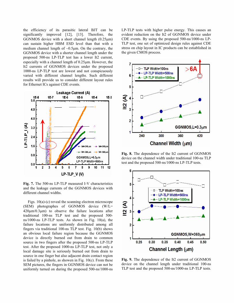
A gate-grounded NMOS (GGNMOS) device (which has been widely used as the on-chip ESD protection device in CMOS ICs) is regarded as the DUT to demonstrate that LP-TLP system can accurately measure its snapback characteristics and secondary breakdown current (It2). The LP-TLP measured I-V characteristics of GGNMOS with a device dimension of W/L= 240 m/0.3 m are shown in Fig. 6(a). In addition, Fig. 6(b)-(g) exhibit the time-domain I-V wafeforms of GGNMOS device at the corresponding points marked in Fig. 6(a). The I-V curves of GGNMOS device will shift from the initial point (A) to the trigger point (B) as the high-voltage DC supply continuously provides the higher energy. After passing through the trigger point (B), the I-V curve will enter the snapback region because the parasitic lateral BJT in the GGNMOS device is turned on. The point C and the point D are the initial point and the middle point in snapback region, respectively. Subsequently, the curve will reach the critical point (E) called the secondary breakdown point of GGNMOS
device. Here, the secondary breakdown current (It2) is defined when the leakage current of DUT exceeds 1 Aafter the LP-TLP stress. If the high-voltage DC supply further raises the charged voltage, the I-V curve will reach the point F into the secondary breakdown region, which causes the permanent damage on the GGNMOS device. From the measured results, the LP-TLP system can efficiently measure the snapback characteristics of GGNMOS device under CDE-like stress. Fig. 6(a) shows that the LP-TLP measured trigger voltage is 5.9V, the holding voltage is 4.2V, and the It2 current is 2.3A. From the aforementioned tests, the LP-TLP system can be used to effectively observe the CDE robustness of DUT.
(a)
(b) (c)
(d) (e)
(f) (g)
Fig. 6. (a) The 500-ns LP-TLP measured I-V characteristic of the GGNMOS device. (b)-(g) The measured time-domain I-V waveforms of GGNMOS device at the corresponding poins marked in (a).
4. Layout Dependence on CDE Robustness
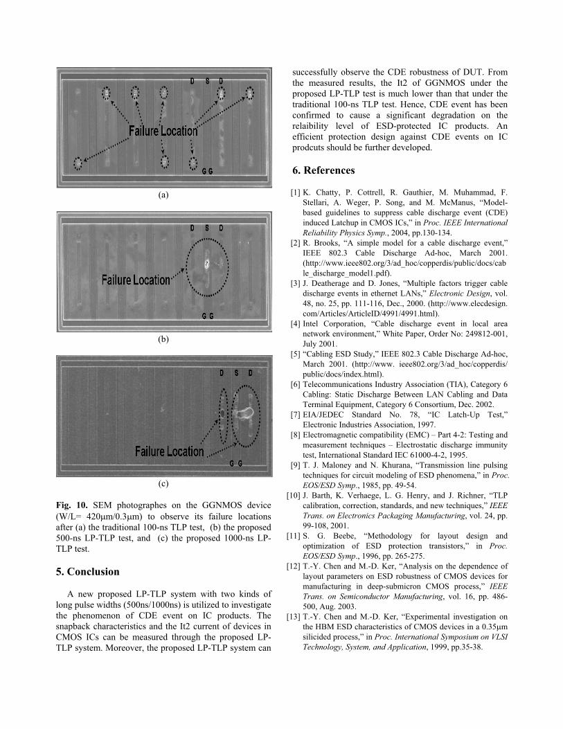
The GGNMOS device fabricated in a 0.25- m CMOS process is studied in this work. The LP-TLP system with two kinds of pulse widths (500ns and 1000ns) are used to measure the snapback I-V curves of GGNMOS device. Fig. 7 exhibits that the 500-ns LP-TLP measured I-V characteristics and the corresponding leakage currents of GGNMOS devices with different channel widths. From the measured results, all GGNMOS devices with different channel widths have distinct snapback characteristics. In addition, the It2 current of the GGNMOS device is linearly increased by increasing the channel width. But, the turn-on resistance of GGNMOS device in snapback region is decreased by increasing the channel width. The It2 current of GGNOS devices with different widths of 240 m, 300 m, 360 m, and 600 m under the proposed 500-ns LP-TLP test are 2.3A, 2.9A, 3.3A, and 5.1A, respectively.
The It2 currents of GGNMOS devices with different channel widths under traditional 100-ns TLP test and the proposed 500-ns/1000-ns LP-TLP tests are compared in Fig. 8. These It2 currents are all linearly increased while the channel width increases. Besides, the It2 current of GGNMOS device under traditional 100-ns TLP test is much greater than those under the proposed 500-ns/1000-ns LP-TLP tests. Attributed to the longer LP-TLP pulse width, the stronger energy is injected into the DUT device, which causes a weak robustness of the device under CDE events.
Fig. 9 shows the dependence of the It2 current of GGNMOS device on the channel length under traditional 100-ns TLP test and the proposed 500-ns/1000-ns LP-TLP tests. The It2 currents of GGNMOS devices with different channel lengths under traditional 100-ns TLP test and the proposed 500-ns/1000-ns LP-TLP tests are quite different. If the GGNMOS device has a shorter enough channel length under traditional 100-ns TLP test,
the efficiency of its parasitic lateral BJT can be significantly improved [12], [13]. Therefore, the GGNMOS device with a short channel length (0.25 m) can sustain higher HBM ESD level than that with a medium channel length of ~0.5 m. On the contrary, the GGNMOS device with a shorter channel length under the proposed 500-ns LP-TLP test has a lower It2 current, especially with a channel length of 0.25 m. However, the It2 currents of GGNMOS devices under the proposed 1000-ns LP-TLP test are lowest and not conspicuously varied with different channel lengths. Such different results will provide us to consider different layout rules for Ethernet ICs against CDE events.
Fig. 7. The 500-ns LP-TLP measured I-V characteristics and the leakage currents of the GGNMOS devices with different channel widths.
Figs. 10(a)-(c) reveal the scanning electron microscope (SEM) photographes of GGNMOS device (W/L= 420 m/0.3 m) to observe the failure locations after traditional 100-ns TLP test and the proposed 500-ns/1000-ns LP-TLP tests. As shown in Fig. 10(a), the failure locations are uniformly distributed among all fingers via traditional 100-ns TLP test. Fig. 10(b) shows an obvious local failure region because the GGNMOS device is directly burned out from drain to common source in two fingers after the proposed 500-ns LP-TLP test. After the proposed 1000-ns LP-TLP test, not only a local damage site is seriously burned out from drain to source in one finger but also adjacent drain contact region is failed by a pinhole, as showen in Fig. 10(c). From these SEM pictures, the fingers in GGNMOS device can not be uniformly turned on during the proposed 500-ns/1000-ns
LP-TLP tests with higher pulse energy. This causes an evident reduction on the It2 of GGNMOS device under CDE events. By using the proposed 500-ns/1000-ns LP-TLP test, one set of optimized design rules against CDE stress on chip layout in IC products can be estiablished in the given CMOS process.
Fig. 8. The dependence of the It2 current of GGNMOS device on the channel width under traditional 100-ns TLP test and the proposed 500-ns/1000-ns LP-TLP tests.
Fig. 9. The dependence of the It2 current of GGNMOS device on the channel length under traditional 100-ns TLP test and the proposed 500-ns/1000-ns LP-TLP tests.
(a)
(b)
(c)
Fig. 10. SEM photographes on the GGNMOS device (W/L= 420 m/0.3 m) to observe its failure locations after (a) the traditional 100-ns TLP test, (b) the proposed 500-ns LP-TLP test, and (c) the proposed 1000-ns LP-TLP test.
5. Conclusion
A new proposed LP-TLP system with two kinds of long pulse widths (500ns/1000ns) is utilized to investigate the phenomenon of CDE event on IC products. The snapback characteristics and the It2 current of devices in CMOS ICs can be measured through the proposed LP-TLP system. Moreover, the proposed LP-TLP system can
successfully observe the CDE robustness of DUT. From the measured results, the It2 of GGNMOS under the proposed LP-TLP test is much lower than that under the traditional 100-ns TLP test. Hence, CDE event has been confirmed to cause a significant degradation on the relaibility level of ESD-protected IC products. An efficient protection design against CDE events on IC prodcuts should be further developed.
6. References
[1] K. Chatty, P. Cottrell, R. Gauthier, M. Muhammad, F. Stellari, A. Weger, P. Song, and M. McManus, “Model-based guidelines to suppress cable discharge event (CDE) induced Latchup in CMOS ICs,” in Proc. IEEE International Reliability Physics Symp., 2004, pp.130-134.
[2] R. Brooks, “A simple model for a cable discharge event,” IEEE 802.3 Cable Discharge Ad-hoc, March 2001. (http://www.ieee802.org/3/ad_hoc/copperdis/public/docs/cable_discharge_model1.pdf).
[3] J. Deatherage and D. Jones, “Multiple factors trigger cable discharge events in ethernet LANs,” Electronic Design, vol. 48, no. 25, pp. 111-116, Dec., 2000. (http://www.elecdesign. com/Articles/ArticleID/4991/4991.html).
[4] Intel Corporation, “Cable discharge event in local area network environment,” White Paper, Order No: 249812-001, July 2001.
[5] “Cabling ESD Study,” IEEE 802.3 Cable Discharge Ad-hoc, March 2001. (http://www. ieee802.org/3/ad_hoc/copperdis/public/docs/index.html).
[6] Telecommunications Industry Association (TIA), Category 6 Cabling: Static Discharge Between LAN Cabling and Data Terminal Equipment, Category 6 Consortium, Dec. 2002.
[7] EIA/JEDEC Standard No. 78, “IC Latch-Up Test,” Electronic Industries Association, 1997.
[8] Electromagnetic compatibility (EMC) – Part 4-2: Testing and measurement techniques – Electrostatic discharge immunity test, International Standard IEC 61000-4-2, 1995.
[9] T. J. Maloney and N. Khurana, “Transmission line pulsing techniques for circuit modeling of ESD phenomena,” in Proc.EOS/ESD Symp., 1985, pp. 49-54.
[10] J. Barth, K. Verhaege, L. G. Henry, and J. Richner, “TLP calibration, correction, standards, and new techniques,” IEEETrans. on Electronics Packaging Manufacturing, vol. 24, pp. 99-108, 2001.
[11] S. G. Beebe, “Methodology for layout design and optimization of ESD protection transistors,” in Proc.EOS/ESD Symp., 1996, pp. 265-275.
[12] T.-Y. Chen and M.-D. Ker, “Analysis on the dependence of layout parameters on ESD robustness of CMOS devices for manufacturing in deep-submicron CMOS process,” IEEETrans. on Semiconductor Manufacturing, vol. 16, pp. 486-500, Aug. 2003.
[13] T.-Y. Chen and M.-D. Ker, “Experimental investigation on the HBM ESD characteristics of CMOS devices in a 0.35 msilicided process,” in Proc. International Symposium on VLSI Technology, System, and Application, 1999, pp.35-38.