Embed Size (px)
Citation preview

MCP6N11500 kHz, 800 µA Instrumentation Amplifier
Features• Rail-to-Rail Input and Output• Gain Set by 2 External Resistors• Minimum Gain (GMIN) Options:
1, 2, 5, 10 or 100 V/V• Common Mode Rejection Ratio (CMRR): 115 dB
(typical, GMIN = 100)• Power Supply Rejection Ratio (PSRR): 112 dB
(typical, GMIN = 100)• Bandwidth: 500 kHz (typical, Gain = GMIN)• Supply Current: 800 μA/channel (typical)• Single Channel• Enable/VOS Calibration pin: (EN/CAL)• Power Supply: 1.8V to 5.5V• Extended Temperature Range: -40°C to +125°C
Typical Applications• High Side Current Sensor• Wheatstone Bridge Sensors• Difference Amplifier with Level Shifting• Power Control Loops
Design Aids• Microchip Advanced Part Selector (MAPS)• Demonstration Board• Application Notes
Block Diagram
DescriptionMicrochip Technology Inc. offers the single MCP6N11instrumentation amplifier (INA) with Enable/VOS Cali-bration pin (EN/CAL) and several minimum gainoptions. It is optimized for single-supply operation withrail-to-rail input (no common mode crossover distor-tion) and output performance.
Two external resistors set the gain, minimizing gainerror and drift-over temperature. The reference voltage(VREF) shifts the output voltage (VOUT).
The supply voltage range (1.8V to 5.5V) is low enoughto support many portable applications. All devices arefully specified from -40°C to +125°C.
These parts have five minimum gain options (1, 2, 5, 10and 100 V/V). This allows the user to optimize the inputoffset voltage and input noise for different applications.
Typical Application Circuit
Package Types
RF VFG
VOUT
Low Power
VSSVDD
EN/CAL
VOUT
VOS Calibration
VREF
RM4
GM2 ΣI2VREF
I4
GM3
I3
VTR
RG
VIP
VIM
GM1
I1VIP
VIM
POR
10 ΩVDD
IDD
VBAT+1.8V
to+5.5V
VOUT
VREF
VFG
RF
RG
200 kΩ
10 kΩ
U1MCP6N11
MCP6N11SOIC
VIP
VIM
VSS
VDD
VOUT
1
234
8
765 VREF
EN/CALVFG
MCP6N112×3 TDFN *
VIP
VIM
VSS
VDD
VOUT
1
2
34
8
7
65 VREF
EN/CALVFG
* Includes Exposed Thermal Pad (EP); see Table 3-1.
EP9
© 2011 Microchip Technology Inc. DS25073A-page 1

MCP6N11
Minimum Gain OptionsTable 1 shows key specifications that differentiatebetween the different minimum gain (GMIN) options.See Section 1.0 “Electrical Characteristics”,Section 6.0 “Packaging Information” and ProductIdentification System for further information on GMIN.TABLE 1: KEY DIFFERENTIATING SPECIFICATIONS
Part No.GMIN(V/V)Nom.
VOS(±mV)Max.
∆VOS/∆TA(±µV/°C)
Typ.
CMRR (dB)Min.
VDD = 5.5V
PSRR(dB)Min.
VDMH(V)
Max.
GBWP(MHz)Nom.
Eni(µVP-P)Nom.
(f = 0.1 to 10 Hz)
eni(nV/√Hz)
Nom.(f = 10 kHz)
MCP6N11-001 1 3.0 90 70 62 2.70 0.50 570 950MCP6N11-002 2 2.0 45 78 68 1.35 1.0 285 475MCP6N11-005 5 0.85 18 80 75 0.54 2.5 114 190MCP6N11-010 10 0.50 9.0 81 81 0.27 5.0 57 95MCP6N11-100 100 0.35 2.7 88 86 0.027 35 18 35
DS25073A-page 2 © 2011 Microchip Technology Inc.

MCP6N11
1.0 ELECTRICAL CHARACTERISTICS
1.1 Absolute Maximum Ratings †VDD – VSS .......................................................................6.5VCurrent at Input Pins †† ...............................................±2 mAAnalog Inputs (VIP and VIM) †† ..... VSS – 1.0V to VDD + 1.0VAll Other Inputs and Outputs ......... VSS – 0.3V to VDD + 0.3VDifference Input Voltage....................................... |VDD – VSS|Output Short Circuit Current ................................ContinuousCurrent at Output and Supply Pins ............................±30 mAStorage Temperature ...................................-65°C to +150°CMax. Junction Temperature ........................................ +150°CESD protection on all pins (HBM, CDM, MM) .≥ 2 kV, 1.5 kV, 300V
† Notice: Stresses above those listed under “AbsoluteMaximum Ratings” may cause permanent damage tothe device. This is a stress rating only and functionaloperation of the device at those or any otherconditions above those indicated in the operationallistings of this specification is not implied. Exposure tomaximum rating conditions for extended periods mayaffect device reliability.†† See Section 4.2.1.2 “Input Voltage Limits” andSection 4.2.1.3 “Input Current Limits”.
1.2 Specifications
TABLE 1-1: DC ELECTRICAL SPECIFICATIONSElectrical Characteristics: Unless otherwise indicated, TA = +25°C, VDD = 1.8V to 5.5V, VSS = GND, EN/CAL = VDD, VCM = VDD/2, VDM = 0V, VREF = VDD/2, VL = VDD/2, RL = 10 kΩ to VL and GDM = GMIN; see Figure 1-6 and Figure 1-7.
Parameters Sym Min Typ Max Units GMIN Conditions
Input OffsetInput Offset Voltage, Calibrated
VOS -3.0 — +3.0 mV 1 (Note 2)-2.0 — +2.0 mV 2
-0.85 — +0.85 mV 5-0.50 — +0.50 mV 10-0.35 — +0.35 mV 100
Input Offset Voltage Trim Step
VOSTRM — 0.36 — mV 1— 0.21 — mV 2— 0.077 — mV 5— 0.045 — mV 10— 0.014 — mV 100
Input Offset Voltage Drift
ΔVOS/ΔTA — ±90/GMIN — µV/°C 1 to 10 TA= -40°C to +125°C (Note 3)— ±2.7 — µV/°C 100
Power Supply Rejection Ratio
PSRR 62 82 — dB 168 88 — dB 275 96 — dB 581 102 — dB 1086 112 — dB 100
Note 1: VCM = (VIP + VIM) / 2, VDM = (VIP – VIM) and GDM = 1 + RF/RG.2: The VOS spec limits include 1/f noise effects.3: This is the input offset drift without VOS re-calibration; toggle EN/CAL to minimize this effect.4: These specs apply to both the VIP, VIM input pair (use VCM) and to the VREF, VFG input pair (VREF takes VCM’s place).5: This spec applies to the VIP, VIM, VREF and VFG pins individually.6: Figure 2-11 and Figure 2-19 show the VIVR and VDMR variation over temperature.7: See Section 1.5 “Explanation of DC Error Specs”.
© 2011 Microchip Technology Inc. DS25073A-page 3

MCP6N11
Input Current and Impedance (Note 4)Input Bias Current IB — 10 — pA all
Across Temperature — 80 — pA TA= +85°CAcross Temperature 0 2 5 nA TA= +125°C
Input Offset Current IOS — ±1 — pAAcross Temperature — ±5 — pA TA= +85°CAcross Temperature -1 ±0.05 +1 nA TA= +125°C
Common Mode Input Impedance
ZCM — 1013||6 — Ω||pF
Differential Input Impedance
ZDIFF — 1013||3 — Ω||pF
Input Common Mode Voltage (VCM or VREF) (Note 4)Input Voltage Range VIVL — — VSS − 0.2 V all (Note 5, Note 6)
VIVH VDD + 0.15 — — VCommon Mode Rejection Ratio
CMRR 62 79 — dB 1 VCM = VIVL to VIVH, VDD = 1.8V69 87 — dB 2
75 101 — dB 579 107 — dB 1086 119 — dB 10070 94 — dB 1 VCM = VIVL to VIVH,
VDD = 5.5V78 100 — dB 280 108 — dB 581 114 — dB 1088 115 — dB 100
Common Mode Non-Linearity
INLCM -1000 ±115 +1000 ppm 1 VCM = VIVL to VIVH, VDM = 0V,VDD = 1.8V (Note 7)
-570 ±27 +570 ppm 2-230 ±11 +230 ppm 5-125 ±6 +125 ppm 10-50 ±2 +50 ppm 100
-400 ±42 +400 ppm 1 VCM = VIVL to VIVH, VDM = 0V,VDD = 5.5V (Note 7)
-220 ±10 +220 ppm 2-100 ±4 +100 ppm 5-50 ±2 +50 ppm 10-30 ±1 +30 ppm 100
TABLE 1-1: DC ELECTRICAL SPECIFICATIONS (CONTINUED)Electrical Characteristics: Unless otherwise indicated, TA = +25°C, VDD = 1.8V to 5.5V, VSS = GND, EN/CAL = VDD, VCM = VDD/2, VDM = 0V, VREF = VDD/2, VL = VDD/2, RL = 10 kΩ to VL and GDM = GMIN; see Figure 1-6 and Figure 1-7.
Parameters Sym Min Typ Max Units GMIN Conditions
Note 1: VCM = (VIP + VIM) / 2, VDM = (VIP – VIM) and GDM = 1 + RF/RG.2: The VOS spec limits include 1/f noise effects.3: This is the input offset drift without VOS re-calibration; toggle EN/CAL to minimize this effect.4: These specs apply to both the VIP, VIM input pair (use VCM) and to the VREF, VFG input pair (VREF takes VCM’s place).5: This spec applies to the VIP, VIM, VREF and VFG pins individually.6: Figure 2-11 and Figure 2-19 show the VIVR and VDMR variation over temperature.7: See Section 1.5 “Explanation of DC Error Specs”.
DS25073A-page 4 © 2011 Microchip Technology Inc.

MCP6N11
Input Differential Mode Voltage (VDM) (Note 4)Differential Input Voltage Range
VDML -2.7/GMIN — — V all VREF = (VDD – GDMVDM)/2(Note 6)VDMH — — +2.7/GMIN V
Differential Gain Error gE -1 ±0.13 +1 % VDM = VDML to VDMH,Differential Gain Drift ΔgE/ΔTA — ±0.0006 — %/°C VREF = (VDD – GDMVDM)/2Differential Non-Linearity
INLDM -500 ±30 +500 ppm 1 (Note 7)-800 ±40 +800 ppm 2, 5
-2000 ±100 +2000 ppm 10, 100DC Open-Loop Gain AOL 61 84 — dB 1 VDD = 1.8V,
68 90 — dB 2 VOUT = 0.2V to 1.6V76 98 — dB 578 104 — dB 1086 116 — dB 10070 94 — dB 1 VDD = 5.5V,77 100 — dB 2 VOUT = 0.2V to 5.3V84 108 — dB 590 114 — dB 1097 125 — dB 100
OutputMinimum Output Voltage Swing
VOL — — VSS + 15 mV all VDM = -VDD/(2GDM),VDD = 1.8V,VREF = VDD/2 – 1V
— — VSS + 25 mV VDM = -VDD/(2GDM),VDD = 5.5V,VREF = VDD/2 – 1V
Maximum Output Voltage Swing
VOH VDD − 15 — — mV VDM = VDD/(2GDM),VDD = 1.8V,VREF = VDD/2 + 1V
VDD − 25 — — mV VDM = VDD/(2GDM),VDD = 5.5V,VREF = VDD/2 + 1V
Output Short Circuit Current
ISC — ±8 — mA VDD = 1.8V— ±30 — mA VDD = 5.5V
Power SupplySupply Voltage VDD 1.8 — 5.5 V allQuiescent Current per Amplifier
IQ 0.5 0.8 1.1 mA IO = 0
POR Trip Voltage VPRL 1.1 1.4 — VVPRH — 1.4 1.7 V
TABLE 1-1: DC ELECTRICAL SPECIFICATIONS (CONTINUED)Electrical Characteristics: Unless otherwise indicated, TA = +25°C, VDD = 1.8V to 5.5V, VSS = GND, EN/CAL = VDD, VCM = VDD/2, VDM = 0V, VREF = VDD/2, VL = VDD/2, RL = 10 kΩ to VL and GDM = GMIN; see Figure 1-6 and Figure 1-7.
Parameters Sym Min Typ Max Units GMIN Conditions
Note 1: VCM = (VIP + VIM) / 2, VDM = (VIP – VIM) and GDM = 1 + RF/RG.2: The VOS spec limits include 1/f noise effects.3: This is the input offset drift without VOS re-calibration; toggle EN/CAL to minimize this effect.4: These specs apply to both the VIP, VIM input pair (use VCM) and to the VREF, VFG input pair (VREF takes VCM’s place).5: This spec applies to the VIP, VIM, VREF and VFG pins individually.6: Figure 2-11 and Figure 2-19 show the VIVR and VDMR variation over temperature.7: See Section 1.5 “Explanation of DC Error Specs”.
© 2011 Microchip Technology Inc. DS25073A-page 5

MCP6N11
TABLE 1-2: AC ELECTRICAL SPECIFICATIONSElectrical Characteristics: Unless otherwise indicated, TA = 25°C, VDD = 1.8V to 5.5V, VSS = GND, EN/CAL = VDD, VCM = VDD/2, VDM = 0V, VREF = VDD/2, VL = VDD/2, RL = 10 kΩ to VL, CL = 60 pF and GDM = GMIN; see Figure 1-6 and Figure 1-7.
Parameters Sym Min Typ Max Units GMIN Conditions
AC ResponseGain Bandwidth Product
GBWP — 0.50 GMIN — MHz 1 to 10— 35 — MHz 100
Phase Margin PM — 70 — ° allOpen-Loop Output Impedance
ROL — 0.9 — kΩ 1 to 10— 0.6 — kΩ 100
Power Supply Rejection Ratio
PSRR — 94 — dB all f < 10 kHz
Common Mode Rejection Ratio
CMRR — 104 — dB 1 to 10 f < 10 kHz— 94 — dB 100 f < 10 kHz
Step ResponseSlew Rate SR — 3 — V/µs 1 to 10 VDD = 1.8V
— 9 — V/µs VDD = 5.5V— 2 — V/µs 100 VDD = 1.8V— 6 — V/µs VDD = 5.5V
Overdrive Recovery,Input Common Mode
tIRC — 10 — µs all VCM = VSS – 1V (or VDD + 1V) to VDD/2,GDMVDM = ±0.1V, 90% of VOUT change
Overdrive Recovery,Input Differential Mode
tIRD — 5 — µs VDM = VDML – (0.5V)/GMIN(or VDMH + (0.5V)/GMIN) to 0V,
VREF = (VDD – GDMVDM)/2,90% of VOUT change
Overdrive Recovery, Output
tOR — 8 — µs GDM = 2GMIN, GDMVDM = 0.5VDD to 0V,VREF = 0.75VDD (or 0.25VDD),90% of VOUT change
NoiseInput Noise Voltage Eni — 570/GMIN — µVP-P 1 to 10 f = 0.1 Hz to 10 Hz
— 18 — µVP-P 100Input Noise Voltage Density
eni — 950/GMIN — nV/√Hz 1 to 10 f = 100 kHz— 35 — nV/√Hz 100
Input Current Noise Density
ini — 1 — fA/√Hz all f = 1 kHz
DS25073A-page 6 © 2011 Microchip Technology Inc.

MCP6N11
TABLE 1-3: DIGITAL ELECTRICAL SPECIFICATIONSElectrical Characteristics: Unless otherwise indicated, TA = 25°C, VDD = 1.8V to 5.5V, VSS = GND, EN/CAL = VDD, VCM = VDD/2, VDM = 0V, VREF = VDD/2, VL = VDD/2, RL = 10 kΩ to VL, CL = 60 pF and GDM = GMIN; see Figure 1-6 and Figure 1-7.
Parameters Sym Min Typ Max Units GMIN Conditions
EN/CAL Low SpecificationsEN/CAL Logic Threshold, Low
VIL VSS — 0.2 VDD V all
EN/CAL Input Current, Low
IENL — -0.1 — nA EN/CAL = 0V
GND Current ISS -7 -2.5 — µA EN/CAL = 0V, VDD = 5.5VAmplifier Output Leakage IO(LEAK) — 10 — nA EN/CAL = 0V
EN/CAL High SpecificationsEN/CAL Logic Threshold, High
VIH 0.8 VDD VDD V all
EN/CAL Input Current, High
IENH — -0.01 — nA EN/CAL = VDD
EN/CAL Dynamic SpecificationsEN/CAL Input Hysteresis VHYST — 0.2 — V all
EN/CAL Low to Amplifier Output High-Z Turn-off Time
tOFF — 3 10 µs EN/CAL = 0.2VDD to VOUT = 0.1(VDD/2), VDMGDM = 1 V, VL = 0V
EN/CAL High to Amplifier OutputOn Time
tON 12 20 28 ms EN/CAL = 0.8VDD to VOUT = 0.9(VDD/2), VDMGDM = 1 V, VL = 0V
EN/CAL Low to EN/CAL High low time
tENLH 100 — — µs Minimum time before externallyreleasing EN/CAL (Note 1)
Amplifier On to EN/CAL Low Setup Time
tENOL — 100 — µs
POR Dynamic SpecificationsVDD ↓ to Output Off tPHL — 10 — µs all VL = 0V, VDD = 1.8V to
VPRL – 0.1V step,90% of VOUT change
VDD ↑ to Output On tPLH 140 250 360 ms VL = 0V, VDD = 0V to VPRH + 0.1V step,90% of VOUT change
Note 1: For design guidance only; not tested.
TABLE 1-4: TEMPERATURE SPECIFICATIONSElectrical Characteristics: Unless otherwise indicated, all limits are specified for: VDD = 1.8V to 5.5V, VSS = GND.
Parameters Sym Min Typ Max Units ConditionsTemperature RangesSpecified Temperature Range TA -40 — +125 °C
Operating Temperature Range TA -40 — +125 °C (Note 1)Storage Temperature Range TA -65 — +150 °C
Thermal Package ResistancesThermal Resistance, 8L-SOIC θJA — 150 — °C/WThermal Resistance, 8L-TDFN (2×3) θJA — 53 — °C/WNote 1: Operation must not cause TJ to exceed the Absolute Maximum Junction Temperature specification (+150°C).
© 2011 Microchip Technology Inc. DS25073A-page 7

MCP6N11
1.3 Timing DiagramsFIGURE 1-1: Common Mode Input Overdrive Recovery Timing Diagram.
FIGURE 1-2: Differential Mode Input Overdrive Recovery Timing Diagram.
FIGURE 1-3: Output Overdrive Recovery Timing Diagram.
FIGURE 1-4: POR Timing Diagram.
FIGURE 1-5: EN/CAL Timing Diagram.
VOUT
tIRC
VDM
VCM
±(1V)/GDM
VOUT
tIRD
VCM
VDM
VDD/2
VOUT
tOR
VCM
VDM
VDD/2
1.8V
VPRL – 0.1V
High-ZVOUT
VDD
tPHLtPLH
VPRH + 0.1V
0V
High-ZVOUT
EN/CAL
tOFFtON
tENLH
tENOL
DS25073A-page 8 © 2011 Microchip Technology Inc.

MCP6N11
1.4 DC Test Circuits1.4.1 INPUT OFFSET TEST CIRCUITFigure 1-6 is used for testing the INA’s input offseterrors and input voltage range (VE, VIVL and VIVH; seeSection 1.5.1 “Input Offset Related Errors” andSection 1.5.2 “Input Offset Common Mode Non-linearity”). U2 is part of a control loop that forces VOUTto equal VCNT; U1 can be set to any bias point.
FIGURE 1-6: Test Circuit for Common Mode (Input Offset).When MCP6N11 is in its normal range of operation, theDC output voltages are (where VE is the sum of inputoffset errors and gE is the gain error):
EQUATION 1-1:
Table 1-5 gives the recommended RF and RG valuesfor different GMIN options.
1.4.2 DIFFERENTIAL GAIN TEST CIRCUITFigure 1-7 is used for testing the INA’s differential gainerror, non-linearity and input voltage range (gE, INLDM,VDML and VDMH; see Section 1.5.3 “Differential GainError and Non-linearity”). RF and RG are 0.01% foraccurate gain error measurements.
FIGURE 1-7: Test Circuit for Differential Mode.The output voltages are (where VE is the sum of inputoffset errors and gE is the gain error):
EQUATION 1-2:
To keep VREF, VFG and VOUT within their ranges, set:
EQUATION 1-3:
Table 1-6 shows the recommended RF and RG. Theyproduce a 10 kΩ load; VL can usually be left open.
TABLE 1-5: SELECTING RF AND RGGMIN(V/V)Nom.
RF(Ω)
Nom.
RG(Ω)
Nom.
GDM(V/V)Nom.
GDMVOS(±V)Max.
BW(kHz)Nom.
1 100k 499 201.4 0.60 2.52 0.40 5.05 100k 100 1001 0.85 2.5
10 0.50 5.0100 0.35 35
RL
VCM 100 nF
VDD
2.2 µF
VREF
VL
12.7 kΩVM
100 nF CCNT
U1
MCP6N11
U2
MCP6H01
VCNT
63.4 kΩ
RG
RF
RCNT63.4 kΩ
VOUT
10 nF
1 kΩ1 kΩ
GDM 1 RF RG⁄+=VOUT VCNT=
VM VREF GDM 1 gE+( )VE+=
TABLE 1-6: SELECTING RF AND RGGMIN(V/V)Nom.
RF(Ω)
Nom.
RG(Ω)
Nom.
GDM(V/V)Nom.
1 0 Open 1.0002 4.99k 4.99k 2.0005 8.06k 2.00k 5.030
10 9.09k 1.00k 10.09100 10.0k 100 101.0
RL
6.34 kΩ
1 kΩ
1 kΩ
VCM + VDM/2
+100 nF
VOUT
RF
RG
VM–
100 nF
VDD
2.2 µF
6.34 kΩ
VREF
VFG
VL
VCM – VDM/2
0.01%
0.01%
U1
MCP6N11
GDM 1 RF RG⁄+=
VM VOUT VREF–=VOUT VREF GDM 1 gE+( ) VDM VE+( )+=
GDM 1 gE+( ) VDM VE+( )=
VREF VDD GDMVDM–( ) 2⁄=
© 2011 Microchip Technology Inc. DS25073A-page 9

MCP6N11
1.5 Explanation of DC Error Specs1.5.1 INPUT OFFSET RELATED ERRORSThe input offset error (VE) is extracted from input offsetmeasurements (see Section 1.4.1 “Input Offset TestCircuit”), based on Equation 1-1:
EQUATION 1-4:
VE has several terms, which assume a linear responseto changes in VDD, VSS, VCM, VOUT and TA (all of whichare in their specified ranges):
EQUATION 1-5:
Equation 1-2 shows how VE affects VOUT.
1.5.2 INPUT OFFSET COMMON MODE NON-LINEARITY
The input offset error (VE) changes non-linearly withVCM. Figure 1-8 shows VE vs. VCM, as well as a linearfit line (VE_LIN) based on VOS and CMRR. The op ampis in standard conditions (ΔVOUT = 0, VDM = 0, etc.).VCM is swept from VIVL to VIVH. The test circuit is inSection 1.4.1 “Input Offset Test Circuit” and VE iscalculated using Equation 1-4.
FIGURE 1-8: Input Offset Error vs. Common Mode Input Voltage.
Based on the measured VE data, we obtain thefollowing linear fit:
EQUATION 1-6:
The remaining error (ΔVE) is described by the CommonMode Non-Linearity spec:
EQUATION 1-7:
The same common mode behavior applies to VE whenVREF is swept, instead of VCM, since both input stagesare designed the same:
EQUATION 1-8:
1.5.3 DIFFERENTIAL GAIN ERROR AND NON-LINEARITY
The differential errors are extracted from differentialgain measurements (see Section 1.4.2 “DifferentialGain Test Circuit”), based on Equation 1-2. Theseerrors are the differential gain error (gE) and the inputoffset error (VE, which changes non-linearly with VDM):
EQUATION 1-9:
These errors are adjusted for the expected output, thenreferred back to the input, giving the differential inputerror (VED) as a function of VDM:
EQUATION 1-10:
VEVM VREF–
GDM 1 gE+( )---------------------------------=
Where:
PSRR, CMRR and AOL are in units of V/V
ΔTA is in units of °C
VDM = 0
VE VOSΔVDD ΔVSS–
PSRR---------------------------------ΔVCMCMRR-----------------
ΔVREFCMRR-----------------+ + +=
ΔVOUT
AOL----------------- ΔTA
ΔVOSΔTA
-------------⋅+ +
V1
V3
VE, VE_LIN (V)
VCM (V)VIVL VIVHVDD/2
V2
VE_LIN
VE
ΔVE
Where:
VE_LIN VOSVCM VDD 2⁄–
CMRR-----------------------------------+=
VOS V2=
1CMRR-----------------
V3 V1–VIVH VIVL–------------------------------=
Where:
INLCMmax ΔVE
VIVH VIVL–------------------------------=
ΔVE VE VE_LIN–=
VE_LIN VOSVREF VDD 2⁄–
CMRR-------------------------------------+=
INLCMmax ΔVE
VIVH VIVL–------------------------------=
GDM 1 RF RG⁄+=VM GDM 1 gE+( ) VDM V+ E( )=
VEDVM
GDM------------ VDM–=
DS25073A-page 10 © 2011 Microchip Technology Inc.

MCP6N11
Figure 1-9 shows VED vs. VDM, as well as a linear fitline (VED_LIN) based on VE and gE. The op amp is instandard conditions (ΔVOUT = 0, etc.). VDM is sweptfrom VDML to VDMH.FIGURE 1-9: Differential Input Error vs. Differential Input Voltage.Based on the measured VED data, we obtain thefollowing linear fit:
EQUATION 1-11:
Note that the VE value measured here is not asaccurate as the one obtained in Section 1.5.1 “InputOffset Related Errors”.
The remaining error (ΔVED) is described by theDifferential Mode Non-Linearity spec:
EQUATION 1-12:
V1
V3
VED, VED_LIN (V)
VDM (V)VDML VDMH0
V2
VED_LIN
VED
ΔVED
Where:VED_LIN 1 gE+( )VE gEVDM+=
gEV3 V1–
VDMH VDML–----------------------------------- 1–=
VEV2
1 gE+----------------=
Where:
INLDMmax ΔVED
VDMH VDML–-----------------------------------=
ΔVED VED VED_LIN–=
© 2011 Microchip Technology Inc. DS25073A-page 11

MCP6N11
NOTES:DS25073A-page 12 © 2011 Microchip Technology Inc.

MCP6N11
2.0 TYPICAL PERFORMANCE CURVES
Note: Unless otherwise indicated, TA = +25°C, VDD = 1.8V to 5.5V, VSS = GND, EN/CAL = VDD, VCM = VDD/2, VDM = 0V, VREF = VDD/2, VL = VDD/2, RL = 10 kΩ to VL, CL = 60 pF and GDM = GMIN; see Figure 1-6 and Figure 1-7.
2.1 DC Voltages and Currents
FIGURE 2-1: Normalized Input Offset Voltage, with GMIN = 1 to 10.
FIGURE 2-2: Normalized Input Offset Voltage, with GMIN = 100.
FIGURE 2-3: Normalized Input Offset Voltage Drift, with GMIN = 1 to 10.
FIGURE 2-4: Normalized Input Offset Voltage Drift, with GMIN = 100.
Note: The graphs and tables provided following this note are a statistical summary based on a limited number ofsamples and are provided for informational purposes only. The performance characteristics listed hereinare not tested or guaranteed. In some graphs or tables, the data presented may be outside the specifiedoperating range (e.g., outside specified power supply range) and therefore outside the warranted range.
30%
35%
es
330 SamplesTA =
25%
30%
rren
ce
TA +25°CVDD = 1.8V and 5.5VRTO
20%
f Occ
u
GMIN = 1GMIN = 2 to 10
10%
15%
tage
of GMIN = 2 to 10
5%
10%
Perc
ent
0%
0 6 2 8 4 0 4 8 2 6 0
P
-2.0
-1.6
-1.2
-0.8
-0.4 0.0
0.4
0.8
1.2
1.6
2.0
Normalized Input Offset Voltage; GMINVOS (mV)
12%
14%
s
330 SamplesGMIN = 100
10%
12%
rren
ce
MINTA = +25°CVDD = 1.8V and 5.5VRTO
8%
f Occ
u
6%
tage
of
2%
4%
Perc
ent
0%
2%P
-18
-16
-14
-12
-10 -8 -6 -4 -2 0 2 4 6 8 10 12 14 16 18
Normalized Input Offset Voltage; GMINVOS (mV)
25%
ces No VOS Re-calibration
330 Samples20%
curr
enc p
GMIN = 1 to 10VDD = 5.5VRTO
15%
of O
cc
10%
enta
ge
5%
Perc
e
0%
600
500
400
300
200
100 0
100
200
300
400
500
600
- - -4 - -2 - 2 4
Normalized Input Offset Voltage Drift;GMIN(�VOS/�TA) (μV/°C)
16%18%
ces No VOS Re-calibration
330 Samples
12%14%
curr
enc p
GMIN = 100VDD = 5.5VRTO
8%10%
of O
cc
4%6%8%
enta
ge
0%2%4%
Perc
e
0%
1200
1000
-800
-600
-400
-200 0
200
400
600
800
1000
1200
-1 -1 1 1
Normalized Input Offset Voltage Drift;GMIN(�VOS/�TA) (μV/°C)
© 2011 Microchip Technology Inc. DS25073A-page 13

MCP6N11
Note: Unless otherwise indicated, TA = +25°C, VDD = 1.8V to 5.5V, VSS = GND, EN/CAL = VDD, VCM = VDD/2, VDM = 0V, VREF = VDD/2, VL = VDD/2, RL = 10 kΩ to VL, CL = 60 pF and GDM = GMIN; see Figure 1-6 and Figure 1-7.FIGURE 2-5: Normalized Input Offset Voltage vs. Power Supply Voltage, with VCM = 0V and GMIN = 1 to 10.
FIGURE 2-6: Normalized Input Offset Voltage vs. Power Supply Voltage, with VCM = 0V and GMIN = 100.
FIGURE 2-7: Normalized Input Offset Voltage vs. Power Supply Voltage, with VCM = VDD and GMIN = 1 to 10.
FIGURE 2-8: Normalized Input Offset Voltage vs. Power Supply Voltage, with VCM = VDD and GMIN = 100.
FIGURE 2-9: Normalized Input Offset Voltage vs. Output Voltage, with GMIN = 1 to 10.
FIGURE 2-10: Normalized Input Offset Voltage vs. Output Voltage, with GMIN = 100.
-0.50.00.51.01.52.02.5
d In
put O
ffset
Vol
tage
;G
MIN
V OS
(mV)
-40°C
-2.5-2.0-1.5-1.0
0.0
0.5
1.0
1.5
2.0
2.5
3.0
3.5
4.0
4.5
5.0
5.5
6.0
6.5
Nor
mal
ized G
Power Supply Voltage
Representative PartVCM = VSSGMIN = 1 to 10RTO
+25°C+85°C
+125°C
2025
age;
1015
et V
olta
05
10
t Offs
eS
(mV)
-50
d In
put
GM
INV O
-15-10
mal
ized G
Representative PartVCM = VSS
-40°C25°C85°C
-25-20
Nor
m CM SSGMIN = 100RTO
85°C125°C
0.0
0.5
1.0
1.5
2.0
2.5
3.0
3.5
4.0
4.5
5.0
5.5
6.0
6.5
Power Supply Voltage
-0 4-0.20.00.20.40.60.81.01.2
d In
put O
ffset
Vol
tage
;G
MIN
V OS
(mV)
Representative PartVCM = VDDGMIN = 1 to 10RTO
-40°C+25°C+85°C+125°C
-1.2-1.0-0.8-0.6-0.4
0.0
0.5
1.0
1.5
2.0
2.5
3.0
3.5
4.0
4.5
5.0
5.5
6.0
6.5
Nor
mal
ize d G
Power Supply Voltage
-202468
10
d In
put O
ffset
Vol
tage
;G
MIN
V OS
(mV)
Representative PartVCM = VDDGMIN = 100RTO
-10-8-6-4
0.0
0.5
1.0
1.5
2.0
2.5
3.0
3.5
4.0
4.5
5.0
5.5
6.0
6.5
Nor
mal
ized G
Power Supply Voltage
-40°C+25°C+85°C+125°C
-0.5
0.0
0.5
1.0
1.5
2.0
d In
put O
ffset
Vol
tage
;G
MIN
V OS
(mV)
Representative PartGMIN = 1 to 10RTO
VDD = 5.5V
VDD = 1.8V
-2.0
-1.5
-1.0
0.0 0.5 1.0 1.5 2.0 2.5 3.0 3.5 4.0 4.5 5.0 5.5
Nor
mal
ized G
Output Voltage (V)
2-10123456
d In
put O
ffset
Vol
tage
;G
MIN
V OS
(mV)
Representative PartGMIN = 100RTO
VDD = 5.5V
VDD = 1.8V
-6-5-4-3-2
0.0 0.5 1.0 1.5 2.0 2.5 3.0 3.5 4.0 4.5 5.0 5.5
Nor
mal
ized G
Output Voltage (V)
DS25073A-page 14 © 2011 Microchip Technology Inc.
MCP6N11
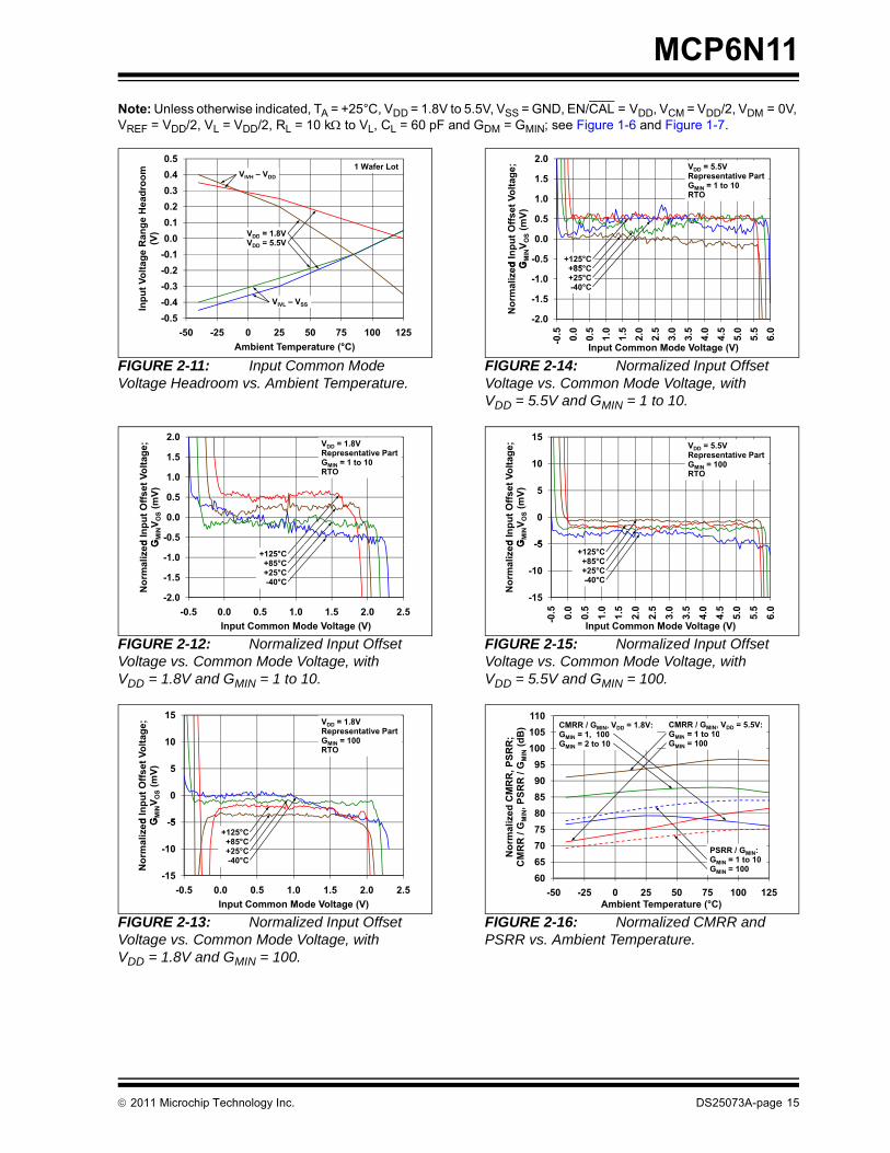
Note: Unless otherwise indicated, TA = +25°C, VDD = 1.8V to 5.5V, VSS = GND, EN/CAL = VDD, VCM = VDD/2, VDM = 0V, VREF = VDD/2, VL = VDD/2, RL = 10 kΩ to VL, CL = 60 pF and GDM = GMIN; see Figure 1-6 and Figure 1-7.FIGURE 2-11: Input Common Mode Voltage Headroom vs. Ambient Temperature.
FIGURE 2-12: Normalized Input Offset Voltage vs. Common Mode Voltage, with VDD = 1.8V and GMIN = 1 to 10.
FIGURE 2-13: Normalized Input Offset Voltage vs. Common Mode Voltage, with VDD = 1.8V and GMIN = 100.
FIGURE 2-14: Normalized Input Offset Voltage vs. Common Mode Voltage, with VDD = 5.5V and GMIN = 1 to 10.
FIGURE 2-15: Normalized Input Offset Voltage vs. Common Mode Voltage, with VDD = 5.5V and GMIN = 100.
FIGURE 2-16: Normalized CMRR and PSRR vs. Ambient Temperature.
0.40.5
om
1 Wafer LotVIVH – VDD
0.20.3
Hea
droo
0 00.10.2
ange
HV) VDD = 1.8V
0 2-0.10.0
tage
Ra (V
DDVDD = 5.5V
-0.3-0.2
ut V
olt
-0.5-0.4In
p VIVL – VSS
-50 -25 0 25 50 75 100 125Ambient Temperature (°C)
-0.5
0.0
0.5
1.0
1.5
2.0
d In
put O
ffset
Vol
tage
;G
MIN
V OS
(mV)
VDD = 1.8VRepresentative PartGMIN = 1 to 10RTO
-2.0
-1.5
-1.0
-0.5 0.0 0.5 1.0 1.5 2.0 2.5
Nor
mal
ized G
Input Common Mode Voltage (V)
+125°C+85°C+25°C-40°C
-5
0
5
10
15
d In
put O
ffset
Vol
tage
;G
MIN
V OS
(mV)
VDD = 1.8VRepresentative PartGMIN = 100RTO
-15
-10
-5
-0.5 0.0 0.5 1.0 1.5 2.0 2.5
Nor
mal
ized G
Input Common Mode Voltage (V)
+125°C+85°C+25°C-40°C
-0.5
0.0
0.5
1.0
1.5
2.0
d In
put O
ffset
Vol
tage
;G
MIN
V OS
(mV)
VDD = 5.5VRepresentative PartGMIN = 1 to 10RTO
+125°C+85
-2.0
-1.5
-1.0
-0.5 0.0
0.5
1.0
1.5
2.0
2.5
3.0
3.5
4.0
4.5
5.0
5.5
6.0
Nor
mal
ized G
Input Common Mode Voltage (V)
+85°C+25°C-40°C
-5
0
5
10
15
d In
put O
ffset
Vol
tage
;G
MIN
V OS
(mV)
VDD = 5.5VRepresentative PartGMIN = 100RTO
-15
-10
-5-0
.5 0.0
0.5
1.0
1.5
2.0
2.5
3.0
3.5
4.0
4.5
5.0
5.5
6.0
Nor
mal
ized G
Input Common Mode Voltage (V)
+125°C+85°C+25°C-40°C
105110
B) CMRR / GMIN, VDD = 1.8V:
GMIN = 1 100CMRR / GMIN, VDD = 5.5V:GMIN = 1 to 10
95100
PSR
R;
GM
IN(d
B GMIN 1, 100GMIN = 2 to 10
GMIN 1 to 10GMIN = 100
859095
MR
R,P
SRR
/ G
8085
ized
CM
GM
IN, P
S
7075
Nor
mal
RR
/ G
PSRR / GMIN:
6065
NC
M
PSRR / GMIN:GMIN = 1 to 10GMIN = 100
60-50 -25 0 25 50 75 100 125
Ambient Temperature (°C)
© 2011 Microchip Technology Inc. DS25073A-page 15

MCP6N11
Note: Unless otherwise indicated, TA = +25°C, VDD = 1.8V to 5.5V, VSS = GND, EN/CAL = VDD, VCM = VDD/2, VDM = 0V, VREF = VDD/2, VL = VDD/2, RL = 10 kΩ to VL, CL = 60 pF and GDM = GMIN; see Figure 1-6 and Figure 1-7.FIGURE 2-17: Normalized DC Open-Loop Gain vs. Ambient Temperature.
FIGURE 2-18: The MCP6N11 Shows No Phase Reversal vs. Common Mode Voltage.
FIGURE 2-19: Normalized Differential Mode Voltage Range vs. Ambient Temperature.
FIGURE 2-20: Normalized Differential Input Error vs. Differential Voltage, with GMIN = 1.
FIGURE 2-21: Normalized Differential Input Error vs. Differential Voltage, with GMIN = 2 to 100.
FIGURE 2-22: The MCP6N11 Shows No Phase Reversal vs. Differential Voltage, with VDD = 5.5V.
105110
ain;
95100
oop
Ga
)
VDD = 5.5VVDD = 1.8V
859095
Ope
n-Lo
MIN
(dB
)
8085
d D
C O
AO
L/ G
M
7075
mal
ized A
GMIN = 1 to 10G = 100
6065
Nor
m GMIN = 100
-50 -25 0 25 50 75 100 125Ambient Temperature (°C)
5.56.0
Representative PartVDD = 5.5V
4 04.55.0
(V)
DD
GDM = 100
3 03.54.0
olta
ge
GDM 100GDM = 1
2.02.53.0
tput
Vo
VIM = -0.20V
1.01.52.0
Out VIM = VDD + 0.15V
0.00.5
-1.0
-0.5 0.0
0.5
1.0
1.5
2.0
2.5
3.0
3.5
4.0
4.5
5.0
5.5
6.0
6.5
Non-inverting Input Voltage; VIP (V)
3.84.0
ut V)
1 Wafer LotGMINVDMH = -GMINVDML
3.43.6
ial I
npu
V DM
H(V RTO
3 03.23.4
ffere
nti
e; G
MIN
V
2.83.0
zed
Dif
Ran
ge
2.42.6
orm
aliz
olta
ge
2.02.2N
o Vo Note: For GMIN = 1,VDMH = minimum of plot value and VDD
-50 -25 0 25 50 75 100 125Axis Title
-2-1012345
ized
Diff
eren
tial I
nput
ror;
GM
INV E
D(m
V)
Representative PartVED = (VOUT – VREF)/GDM – VDMGMIN = 1RTO
VDD = 1.8V
VDD = 5.5V
-5-4-32
-5 -4 -3 -2 -1 0 1 2 3 4 5
Nor
mal Er
r
Normalized Differential Input Voltage;GMINVDM (V)
45
put Representative Part
VED = (VOUT – VREF)/GDM – VDM
23
tial I
npm
V)
VED (VOUT VREF)/GDM VDMGMIN = 2 to 100RTO
01
iffer
ent
MIN
V ED
(
-2-10
ized
Di
ror;
GM
-4-32
Nor
mal Er
r
-54
-5 -4 -3 -2 -1 0 1 2 3 4 5
N
-5 -4 -3 -2 -1 0 1 2 3 4 5Normalized Differential Input Voltage;
GMINVDM (V)
2.02.53.03.54.04.55.05.5
tput
Vol
tage
(V)
Representative PartVDD = 5.5VVREF = (VDD – GDMVDM)/2
0.00.51.01.5
-7 -6 -5 -4 -3 -2 -1 0 1 2 3 4 5 6 7
Out
Differential Input Voltage (V)
GMIN = 1GMIN = 2GMIN = 5GMIN = 10GMIN = 100
DS25073A-page 16 © 2011 Microchip Technology Inc.

MCP6N11
Note: Unless otherwise indicated, TA = +25°C, VDD = 1.8V to 5.5V, VSS = GND, EN/CAL = VDD, VCM = VDD/2, VDM = 0V, VREF = VDD/2, VL = VDD/2, RL = 10 kΩ to VL, CL = 60 pF and GDM = GMIN; see Figure 1-6 and Figure 1-7.FIGURE 2-23: Input Bias and Offset Currents vs. Ambient Temperature, with VDD = +5.5V.
FIGURE 2-24: Input Bias Current vs. Input Voltage (below VSS).
FIGURE 2-25: Input Bias and Offset Currents vs. Common Mode Input Voltage, with TA = +85°C.
FIGURE 2-26: Input Bias and Offset Currents vs. Common Mode Input Voltage, with TA = +125°C.
FIGURE 2-27: Output Voltage Headroom vs. Output Current.
FIGURE 2-28: Output Voltage Headroom vs. Ambient Temperature.
1.E-10
1.E-09
1.E-08
s, O
ffset
Cur
rent
s (A
) VDD = 5.5VVCM = VDD
IB100p
1n
10n
1.E-12
1.E-11
25 45 65 85 105 125
Inpu
t Bia
s
Ambient Temperature (°C)
| IOS |
1p
10p
1 E 09
1.E-08
1.E-07
1.E-06
1.E-05
1.E-04
1.E-03
urre
nt M
agni
tude
(A)
+125°C+85°C+25°C-40°
1m
100μ
10μ
1μ
100n
10n
1n
1.E-12
1.E-11
1.E-10
1.E-09
-1.0 -0.9 -0.8 -0.7 -0.6 -0.5 -0.4 -0.3 -0.2 -0.1 0.0
Inpu
t Cu
Input Voltage (V)
-40 C1n
100p
10p
1p
-200
20406080
100
s, O
ffset
Cur
rent
s (p
A) Representative Part
TA = +85°CVDD = 5.5V
IB
IOS
-100-80-60-40
0.0
0.5
1.0
1.5
2.0
2.5
3.0
3.5
4.0
4.5
5.0
5.5
6.0
Inpu
t Bia
s
Common Mode Input Voltage (V)
1 0-0.50.00.51.01.52.02.5
s, O
ffset
Cur
rent
s (n
A) Representative Part
TA = +125°CVDD = 5.5V
IB
IOS
-2.5-2.0-1.5-1.0
0.0
0.5
1.0
1.5
2.0
2.5
3.0
3.5
4.0
4.5
5.0
5.5
6.0
Inpu
t Bia
s
Common Mode Input Voltage (V)
1000
mV)
oom
(m
V = 1 8V
VDD = 5.5V
100Hea
dro VDD = 1.8V
100lta
geH
VDD – VOH
V V
put V
o VOL – VSS
10
Out
100.1 1 10
Output Current Magnitude (mA)
910
78
(mV) VDD – VOH
567
droo
m VDD = 5.5V
45
ut H
ead
23
Out
pu VDD = 1.8V
01
VOL – VSS0-50 -25 0 25 50 75 100 125
Ambient Temperature (°C)
© 2011 Microchip Technology Inc. DS25073A-page 17

MCP6N11
Note: Unless otherwise indicated, TA = +25°C, VDD = 1.8V to 5.5V, VSS = GND, EN/CAL = VDD, VCM = VDD/2, VDM = 0V, VREF = VDD/2, VL = VDD/2, RL = 10 kΩ to VL, CL = 60 pF and GDM = GMIN; see Figure 1-6 and Figure 1-7.FIGURE 2-29: Output Short Circuit Current vs. Power Supply Voltage.
FIGURE 2-30: Supply Current vs. Power Supply Voltage.
FIGURE 2-31: Supply Current vs. Common Mode Input Voltage.
-100
1020304050
ort C
ircui
t Cur
rent
(mA
)
+125°C+85°C+25°C-40°C
-50-40-30-20
0.0
0.5
1.0
1.5
2.0
2.5
3.0
3.5
4.0
4.5
5.0
5.5
6.0
6.5
Out
put S
ho
Power Supply Voltage (V)
400500600700800900
10001100
ply
Cur
rent
(μA
)
+125°C+85°C+25°C40
0100200300
0.0
0.5
1.0
1.5
2.0
2.5
3.0
3.5
4.0
4.5
5.0
5.5
6.0
6.5
Sup
Power Supply Voltage (V)
-40°C
10001100
800900
μA) VDD = 5.5V
600700
urre
nt (
VDD = 1.8V
400500
ply
Cu
200300Su
p
0100
-0.5 0.0
0.5
1.0
1.5
2.0
2.5
3.0
3.5
4.0
4.5
5.0
5.5
6.0
Common Mode Input Voltage (V)
DS25073A-page 18 © 2011 Microchip Technology Inc.

MCP6N11
Note: Unless otherwise indicated, TA = +25°C, VDD = 1.8V to 5.5V, VSS = GND, EN/CAL = VDD, VCM = VDD/2, VDM = 0V, VREF = VDD/2, VL = VDD/2, RL = 10 kΩ to VL, CL = 60 pF and GDM = GMIN; see Figure 1-6 and Figure 1-7.2.2 Frequency Response
FIGURE 2-32: CMRR vs. Frequency.
FIGURE 2-33: PSRR vs. Frequency.
FIGURE 2-34: Normalized Open-Loop Gain vs. Frequency.
FIGURE 2-35: Normalized Gain Bandwidth Product and Phase Margin vs. Ambient Temperature.
FIGURE 2-36: Closed-Loop Output Impedance vs. Frequency.
FIGURE 2-37: Gain Peaking vs. Normalized Capacitive Load.
405060708090
100
CM
RR
(dB
)
GMIN = 1
VDD = 5.5V
0102030
1.E+03 1.E+04 1.E+05 1.E+06Frequency (Hz)
GMIN 1GMIN = 2GMIN = 5
GMIN = 10GMIN = 100
1k 10k 100k 1M
110120
VDD = 5.5V
8090
100
607080
R (d
B)
405060
PSR
R
203040
GMIN = 1GMIN = 2GMIN = 5
01020 MIN
GMIN = 10GMIN = 100
1.E+03 1.E+04 1.E+05 1.E+06Frequency (Hz)
1k 10k 100k 1M
-90-60
100120
nn
-150-120
6080
op G
ai(°
)
op G
aiN
(dB
) �AOL/GMIN
210-180-150
204060
pen-
Loo
OL/G
MIN
pen-
Loo
AO
L/GM
IN
| AOL/GMIN |
-240-210
020
zed
Op
ase;
AO
zed
Op
tude
;A
-300-270
-40-20
orm
aliz
Pha
orm
aliz
Mag
nit
GMIN = 1GMIN = 2G = 5
-360-330
-80-60 N
o
No M GMIN = 5
GMIN = 10GMIN = 100
1.E+4 1.E+5 1.E+6 1.E+7Frequency (Hz)
10k 100k 1M 10M
140150
0.450.50
h )
120130
0 350.40
°)ndw
ithN
(MH
z)
100110120
0 250.300.35
argi
n (
ain
Ban
WP/
GM
IN
GMIN = 1GMIN = 2 GBWP
90100
0.200.25
hase
Ma
ized
Ga
t; G
BW MIN
GMIN = 5GMIN = 10
GMIN = 100
GBWP
PM
7080
0.100.15 Ph
Nor
mal
iro
duct
5060
0.000.05N P
-50 -25 0 25 50 75 100 125Ambient Temperature (°C)
1.E+04
nce
10k
mpe
dan
GDM/GMIN = 10 GMIN = 1 to 101.E+03
tput
Im)
1kGDM/GMIN 10 MIN
1 E+02op O
ut (�
100
GMIN = 100
1.E+02
sed-
Loo 100
1 E+01
Clo
s
GDM/GMIN = 1101.E+011.E+03 1.E+04 1.E+05 1.E+06 1.E+07
Frequency (Hz)
101k 10k 100k 1M 10M
6
7
GMIN = GDM = 1 GMIN = 10
5
6
B)
GMIN GDM 1= 2= 5
= 10
GDM = 20= 50
4
5
king
(d = 100
3
n Pe
ak GMIN = 100GDM = 200
= 500
2Gai
0
1
01.E+1 1.E+2 1.E+3
Normalized Capacitive Load; CL(GMIN/GDM) (F)10p 100p 1n
© 2011 Microchip Technology Inc. DS25073A-page 19

MCP6N11
Note: Unless otherwise indicated, TA = +25°C, VDD = 1.8V to 5.5V, VSS = GND, EN/CAL = VDD, VCM = VDD/2, VDM = 0V, VREF = VDD/2, VL = VDD/2, RL = 10 kΩ to VL, CL = 60 pF and GDM = GMIN; see Figure 1-6 and Figure 1-7.2.3 Noise
FIGURE 2-38: Normalized Input Noise Voltage Density vs. Frequency.
FIGURE 2-39: Normalized Input Noise Voltage Density vs. Input Common Mode Voltage, with f = 100 Hz.
FIGURE 2-40: Normalized Input Noise Voltage Density vs. Input Common Mode Voltage, with f = 10 kHz.
FIGURE 2-41: Normalized Input Noise Voltage vs. Time, with GMIN = 1 to 10.
FIGURE 2-42: Normalized Input Noise Voltage vs. Time, with GMIN = 100.
1000
age
1mRTO
100e Vo
lta/�
Hz)
100μ
10ut N
oise
Ne n
i(V/
10
GMIN = 100
10
ed In
puty
; GM
I 10μ
1
rmal
ize
Den
sit
1μ GMIN = 10GMIN = 5GMIN = 2
0.1
Nor
100n
GMIN 2GMIN = 1
1.E-1 1.E+0 1.E+1 1.E+2 1.E+3 1.E+4 1.E+5 1.E+6Frequency (Hz)
0.1 100 1k1 10 100k 1M10k
12
14
e
10
12
Volta
g�H
z)
G = 100
8
Noi
se
e ni(
μV/�
VDD = 1.8VVDD = 5.5V
GMIN = 100GMIN = 10GMIN = 5GMIN = 2
6
Inpu
t ; G
MIN
e GMIN = 2GMIN = 1
2
4
mal
ized
en
sity
;
0
2
Nor
m De
f = 100 HzRTO
-0.5 0.0
0.5
1.0
1.5
2.0
2.5
3.0
3.5
4.0
4.5
5.0
5.5
6.0
Common Mode Input Voltage (V)
3 5
4.0
e
3.0
3.5
Volta
g�H
z)
2 0
2.5
Noi
se
e ni(
μV/�
VDD = 1.8VVDD = 5.5V
GMIN = 100GMIN = 10GMIN = 5
1.5
2.0
Inpu
t ; G
MIN
e MINGMIN = 2GMIN = 1
0 5
1.0
mal
ized
en
sity
;
0.0
0.5
Nor
m De
f = 10 kHzRTO
-0.5 0.0
0.5
1.0
1.5
2.0
2.5
3.0
3.5
4.0
4.5
5.0
5.5
6.0
Common Mode Input Voltage (V)
0.40.5
Representative PartGMIN = 1 to 10
Analog NPBW = 0.1 HzSample Rate = 4 SPS
0 20.3
Noi
se;
)
MINRTO
p
0 00.10.2
nput
Nt)
(mV)
-0.10.0
aliz
ed I
GM
INe n
i(t
-0.3-0.2
Nor
ma G
-0.5-0.4
0 5 10 15 20 25 30 35Time (min)
1 5
2.0Representative PartGMIN = 100
Analog NPBW = 0.1 HzSample Rate = 4 SPS
1.0
1.5N
oise
;)
MINRTO
p
0 0
0.5
nput
Nt)
(mV)
-0.5
0.0
aliz
ed I
GM
INe n
i(t
-1.0
Nor
ma G
-2.0
-1.5
0 5 10 15 20 25 30 35Time (min)
DS25073A-page 20 © 2011 Microchip Technology Inc.

MCP6N11
Note: Unless otherwise indicated, TA = +25°C, VDD = 1.8V to 5.5V, VSS = GND, EN/CAL = VDD, VCM = VDD/2, VDM = 0V, VREF = VDD/2, VL = VDD/2, RL = 10 kΩ to VL, CL = 60 pF and GDM = GMIN; see Figure 1-6 and Figure 1-7.2.4 Time Response
FIGURE 2-43: Small Signal Step Response.
FIGURE 2-44: Large Signal Step Response.
FIGURE 2-45: Slew Rate vs. Ambient Temperature.
FIGURE 2-46: Maximum Output Voltage Swing vs. Frequency.
FIGURE 2-47: Common Mode Input Overdrive Recovery Time vs. Normalized Gain.
FIGURE 2-48: Differential Input Overdrive Recovery Time vs. Normalized Gain.
)
VDD = 5.5VGDM = GMIN
mV/
div) RF + RG = 10 k�
e (1
0 m
GMIN = 1 to 10
Volta
g GMIN = 1 to 10GMIN = 100
Out
put
O
0 2 4 6 8 10 12 14 16 18 20Time (μs)
5.05.5
)
VDD = 5.5VGDM = GMIN
4.04.5
mV/
div) DM MIN
RF + RG = 10 k�
3.03.5
e (1
0 m
2.02.5
Volta
ge GMIN = 1 to 10GMIN = 100
1.01.5
Out
put V
0.00.5
O
0.00.0 0.5 1.0 1.5 2.0 2.5 3.0 3.5 4.0 4.5 5.0
Time (μs)
910
78
s)
567
te (V
/μs
G 1 t 10 V = 5 5V
45
ew R
at GMIN = 1 to 10GMIN = 100
VDD = 5.5VVDD = 1.8V
23Sl
e
01
-50 -25 0 25 50 75 100 125Ambient Temperature (°C)
10
ing
ge S
w VDD = 5.5V
1t Vol
ta-P
) VDD = 1.8V1
Out
pu (VP
GMIN = 1 to 10GMIN = 100
xim
um
0
Max
01.E+4 1.E+5 1.E+6
Frequency (Hz)10k 100k 1M
1000
ge s)
GDMVDM = ±1V
100Vo
ltag
t IRC
(μs
VDD = 5.5V100
n M
ode
over
y;VDD = 1.8V
DD
10omm
onve
Rec
o
10
put C
ove
rdriv
GMIN = 100
1
Inp
Ov
GMIN = 1GMIN = 10
1 10 100Normalized Gain; GDM/GMIN
1000
age
s)
100e Vo
ltat IR
D(μ
s
VDD = 5.5V100
al M
ode
over
y;
VDD = 1.8V
VDD 5.5V
10eren
tiave
Rec
o
10
put D
iffe
verd
riv
GMIN = 100
1
Inp Ov
GMIN = 1GMIN = 10
1 10 100Normalized Gain; GDM/GMIN
© 2011 Microchip Technology Inc. DS25073A-page 21

MCP6N11
Note: Unless otherwise indicated, TA = +25°C, VDD = 1.8V to 5.5V, VSS = GND, EN/CAL = VDD, VCM = VDD/2, VDM = 0V, VREF = VDD/2, VL = VDD/2, RL = 10 kΩ to VL, CL = 60 pF and GDM = GMIN; see Figure 1-6 and Figure 1-7.FIGURE 2-49: Output Overdrive Recovery Time vs. Normalized Gain.
FIGURE 2-50: The MCP6N11 Shows No Phase Reversal vs. Common Mode Input Overdrive, with VDD = 5.5V.
FIGURE 2-51: The MCP6N11 Shows No Phase Reversal vs. Differential Input Overdrive, with VDD = 5.5V.
10
100
1000
t Ove
rdriv
e R
ecov
ery;
t OR
(μs)
GMIN = 10
GDM = 2GMINVREF = 0.75VDD
GMIN = 1VDD = 1.8V
VDD = 5.5V
1
10
1 10 100
Out
pu
Normalized Gain; GDM/GMIN
GMIN = 100
5
6
ut
VDD = 5.5VGDMVDM = +0.1VVCM
4
5
, Out
pu
GDMVDM 0.1Vf = 10 kHz
3 Mod
e,es
(V)
2
mm
onVo
ltage
V G 1
0
1
put C
o V VOUT, GMIN = 1VOUT, GMIN = 100
-1
0
Inp
0 10 20 30 40 50 60 70 80 90 100Time (μs)
3
4VDD = 5.5V VIP
2
3
ges
(V)
0
1
Volta
g
VOUT, GMIN = 1VOUT, GMIN = 100
-1
0
Out
put
-2
nput
,O
-4
-3In
VIM
0 10 20 30 40 50 60 70 80 90 100Time (μs)
DS25073A-page 22 © 2011 Microchip Technology Inc.

MCP6N11
Note: Unless otherwise indicated, TA = +25°C, VDD = 1.8V to 5.5V, VSS = GND, EN/CAL = VDD, VCM = VDD/2, VDM = 0V, VREF = VDD/2, VL = VDD/2, RL = 10 kΩ to VL, CL = 60 pF and GDM = GMIN; see Figure 1-6 and Figure 1-7.2.5 Enable/Calibration and POR Responses
FIGURE 2-52: EN/CAL and Output Voltage vs. Time, with VDD = 1.8V.
FIGURE 2-53: EN/CAL and Output Voltage vs. Time, with VDD = 5.5V
FIGURE 2-54: EN/CAL Hysteresis vs. Ambient Temperature.
FIGURE 2-55: EN/CAL Turn On Time vs. Ambient Temperature.
FIGURE 2-56: Power Supply On and Off and Output Voltage vs. Time.
FIGURE 2-57: POR Trip Voltages and Hysteresis vs. Temperature.
0.60.81.01.21.41.61.82.0
, Out
put V
olta
ge (V
)
VDD = 1.8VVL = 0V
INAturns off
CalibrationStarts
INAturns on
-0.20.00.20.4
0 10 20 30 40 50 60 70 80 90 100
EN/C
AL
Time (ms)
EN/CAL VOUT
2.02.53.03.54.04.55.05.56.0
, Out
put V
olta
ge (V
)
VDD = 5.5VVL = 0V
INAturns off
CalibrationStarts
INAturns on
-0.50.00.51.01.5
0 10 20 30 40 50 60 70 80 90 100
EN/C
AL
Time (ms)
EN/CAL VOUT
0.550.60
0.450.50
s (V
)
VDD = 5.5V
0 300.350.40
ster
esi
0 200.250.30
AL
Hys
0.100.150.20
EN/C
A
VDD = 1.8V
0.000.050.10
-50 -25 0 25 50 75 100 125Ambient Temperature (°C)
30
ms)
25
; tO
N(m
VDD = 5.5V
15
20
n Ti
me;
VDD = 1.8V
10
15
urn
On
5
10
/CA
L T
0
5
EN/
-50 -25 0 25 50 75 100 125Ambient Temperature (°C)
1.61.8
e (V
) VL = 0V
1 21.4
Volta
ge
0 81.01.2
utpu
tV
On
0.60.8
ply,
Ou
VDD VOUT
On
0.20.4
er S
up
OffOff
-0.20.0
Pow
e
Calibrating OffOff
0.0 0.1 0.2 0.3 0.4 0.5 0.6 0.7 0.8 0.9 1.0Time (s)
0 06
0.08
0.10
0.12
0.14
0.16
0.18
1 1
1.2
1.3
1.4
1.5
1.6
1.7
R H
yste
resi
s (V
)
Trip
Vol
tage
s (V
)
VPRH – VPRL
VPRH
0.00
0.02
0.04
0.06
0.8
0.9
1.0
1.1
-50 -25 0 25 50 75 100 125
POR
POR
Ambient Temperature (°C)
VPRL
© 2011 Microchip Technology Inc. DS25073A-page 23

MCP6N11
Note: Unless otherwise indicated, TA = +25°C, VDD = 1.8V to 5.5V, VSS = GND, EN/CAL = VDD, VCM = VDD/2, VDM = 0V, VREF = VDD/2, VL = VDD/2, RL = 10 kΩ to VL, CL = 60 pF and GDM = GMIN; see Figure 1-6 and Figure 1-7.FIGURE 2-58: Quiescent Current in Shutdown vs. Power Supply Voltage.
FIGURE 2-59: Output Leakage Current vs. Output Voltage.
0.0
ent; EN/CAL = 0V
-0.5
y C
urre
-1.0
Supp
lyμA
)
-1.5
Pow
erS
I SS
(μ
-2.0ativ
eP
+125°C+85°C
-2.5
Neg
+85 C+25°C-40°C
0.0 0.5 1.0 1.5 2.0 2.5 3.0 3.5 4.0 4.5 5.0 5.5 6.0 6.5Power Supply Voltage (V)
1.E-07
A)
EN/CAL = 0VVDD = 5.5V
100n
1.E-08
rent
(A
+125°C
DD
10n
1.E-09
ge C
urr
+85°C1n
1.E-10
Leak
ag
100p
1.E-11utpu
tL
25°C10p
1.E-12
Ou +25°C
1p0.0 0.5 1.0 1.5 2.0 2.5 3.0 3.5 4.0 4.5 5.0 5.5 6.0
Output Voltage (V)
1p
DS25073A-page 24 © 2011 Microchip Technology Inc.

MCP6N11
3.0 PIN DESCRIPTIONSDescriptions of the pins are listed in Table 3-1.
3.1 Analog Signal InputsThe non-inverting and inverting inputs (VIP, and VIM)are high-impedance CMOS inputs with low biascurrents.
3.2 Analog Feedback InputThe analog feedback input (VFG) is the inverting inputof the second input stage. The external feedbackcomponents (RF and RG) are connected to this pin. It isa high-impedance CMOS input with low bias current.
3.3 Analog Reference InputThe analog reference input (VREF) is the non-invertinginput of the second input stage; it shifts VOUT to itsdesired range. The external gain resistor (RG) isconnected to this pin. It is a high-impedance CMOSinput with low bias current.
3.4 Analog OutputThe analog output (VOUT) is a low-impedance voltageoutput. It represents the differential input voltage(VDM = VIP – VIM), with gain GDM and is shifted byVREF. The external feedback resistor (RF) is connectedto this pin.
3.5 Power Supply PinsThe positive power supply (VDD) is 1.8V to 5.5V higherthan the negative power supply (VSS). For normaloperation, the other pins are between VSS and VDD.
Typically, these parts are used in a single (positive)supply configuration. In this case, VSS is connected toground and VDD is connected to the supply; VDD willneed bypass capacitors.
3.6 Digital Enable and VOS Calibration Input
This input (EN/CAL) is a CMOS, Schmitt-triggeredinput that controls the active, low power and VOScalibration modes of operation. When this pin goes low,the part is placed into a low power mode and the outputis high-Z. When this pin goes high, the amplifier’s inputoffset voltage is corrected by the calibration circuitry,then the output is re-connected to the VOUT pin, whichbecomes low impedance, and the part resumes normaloperation.
3.7 Exposed Thermal Pad (EP)There is an internal connection between the ExposedThermal Pad (EP) and the VSS pin; they must beconnected to the same potential on the Printed CircuitBoard (PCB).
This pad can be connected to a PCB ground plane toprovide a larger heat sink. This improves the packagethermal resistance (θJA).
TABLE 3-1: PIN FUNCTION TABLEMCP6N11
Symbol DescriptionSOIC TDFN
1 1 VFG Feedback Input2 2 VIM Inverting Input3 3 VIP Non-inverting Input4 4 VSS Negative Power Supply5 5 VREF Reference Input6 6 VOUT Output7 7 VDD Positive Power Supply8 8 EN/CAL Enable/VOS Calibrate Digital Input— 9 EP Exposed Thermal Pad (EP); must be connected to VSS
© 2011 Microchip Technology Inc. DS25073A-page 25

MCP6N11
NOTES:DS25073A-page 26 © 2011 Microchip Technology Inc.

MCP6N11
4.0 APPLICATIONSThe MCP6N11 instrumentation amplifier (INA) ismanufactured using Microchip’s state of the art CMOSprocess. It is low cost, low power and high speed,making it ideal for battery-powered applications.
4.1 Basic Performance
4.1.1 STANDARD CIRCUITFigure 4-1 shows the standard circuit configuration forthese INAs. When the inputs and output are in theirspecified ranges, the output voltage is approximately:
EQUATION 4-1:
FIGURE 4-1: Standard Circuit.For normal operation, keep:
• VIP, VIM, VREF and VFG between VIVL and VIVH• VIP – VIM (i.e., VDM) between VDML and VDMH• VOUT between VOL and VOH
4.1.2 ARCHITECTUREFigure 4-2 shows the block diagram for these INAs.
FIGURE 4-2: MCP6N11 Block Diagram.
The input offset voltage (VOS) is corrected by thevoltage VTR. Each time a VOS Calibration event occurs,VTR is updated to the best value (at that moment).These events are triggered by either powering up(monitored by the POR) or by toggling the EN/CAL pinhigh. The current out of GM3 (I3) is constant and verysmall (assumed to be zero in the following discussion).
The input signal is applied to GM1. Equation 4-2 showsthe relationships between the input voltages (VIP andVIM) and the common mode and differential voltages(VCM and VDM).
EQUATION 4-2:
The negative feedback loop includes GM2, RM4, RF andRG. These blocks set the DC open-loop gain (AOL) andthe nominal differential gain (GDM):
EQUATION 4-3:
AOL is very high, so I4 is very small and I1 + I2 ≈ 0. Thismakes the differential inputs to GM1 and GM2 equal inmagnitude and opposite in polarity. Ideally, this gives:
EQUATION 4-4:
For an ideal part, changing VCM, VSS or VDD producesno change in VOUT. VREF shifts VOUT as needed.
The different GMIN options change GM1, GM2 and theinternal compensation capacitor. This results in theperformance trade-offs shown in Table 1.
VOUT ≈ VREF + GDMVDM
Where:
GDM = 1 + RF / RG
VOUT
VIP
VDD
VIM
VREF
VFGRF
RG
U1
MCP6N11
RF VFG
VOUT
Low Power
VSSVDD
EN/CAL
VOUT
VOS Calibration
VREF
RM4
GM2 ΣI2VREF
I4
GM3
I3
VTR
RG
VIP
VIM
GM1
I1VIP
VIM
POR
VIP VCM VDM 2⁄+=VIM VCM VDM 2⁄–=
VCM VIP VIM+( ) 2⁄=VDM VIP VIM–=
AOL GM2RM4=GDM 1 RF RG⁄+=
VFG VREF–( ) VDM=VOUT VDMGDM VREF+=
© 2011 Microchip Technology Inc. DS25073A-page 27

MCP6N11
4.1.3 DC ERRORSSection 1.5 “Explanation of DC Error Specs”defines some of the DC error specifications. Theseerrors are internal to the INA, and can be summarizedas follows:EQUATION 4-5:
The non-linearity specs (INLCM and INLDM) describeerrors that are non-linear functions of VCM and VDM,respectively. They give the maximum excursion fromlinear response over the entire common mode anddifferential ranges.
The input bias current and offset current specs (IB andIOS), together with a circuit’s external input resistances,give an additional DC error. Figure 4-3 shows theresistors that set the DC bias point.
FIGURE 4-3: DC Bias Resistors.The resistors at the main input (RIP and RIM) and itsinput bias currents (IBP and IBM) give the followingchanges in the INA’s bias voltages:
EQUATION 4-6:
The best design results when RIP and RIM are equaland small:
EQUATION 4-7:
The resistors at the feedback input (RR, RF and RG)and its input bias currents (IBR and IBF) give thefollowing changes in the INA’s bias voltages:
EQUATION 4-8:
The best design results when GDMRR and RF are equaland small:
EQUATION 4-9:
Where:
VOUT VREF GDM 1 gE+( ) VDM ΔVED+( )+= GDM 1 gE+( ) VE ΔVE+( )+
Where:
PSRR, CMRR and AOL are in units of V/V
ΔTA is in units of °C
VE VOSΔVDD ΔVSS–
PSRR---------------------------------ΔVCMCMRR-----------------
ΔVREFCMRR-----------------+ + +=
ΔVOUT
AOL----------------- ΔTA
ΔVOSΔTA
-------------⋅+ +
ΔVED INLDM VDMH VDML–( )≤ΔVE INLCM VIVH VIVL–( )≤
VOUT
VIP
VDD
VIM
VREF
RF
RG
RIP
RIM
RR
IBP
IBM VFG
IBF
IBR
U1MCP6N11
Where:
CMRR is in units of V/V
ΔVIP IBPRIP– IB–IOS2--------–⎝ ⎠
⎛ ⎞RIP= =
ΔVIM IBMRIM– IB–IOS2--------+⎝ ⎠
⎛ ⎞RIM= =
ΔVCMΔVIP ΔVIM+
2---------------------------------=
I– BRIP RIM+
2-------------------------⎝ ⎠⎛ ⎞ I– OS
2-----------R– IP RIM+
2----------------------------⎝ ⎠⎛ ⎞+=
ΔVDM ΔVIP ΔVIM–=
IB R– IP RIM+( )IOS2-------- RIP RIM+( )–=
ΔVOUT GDM ΔVDMΔVCMCMRR-----------------+⎝ ⎠
⎛ ⎞=
Where:
RIP = RIM
εRTOL = tolerance of RIP and RIM
ΔVOUT GDMΔVDM≈ GDM 2IBεRTOL IOS–±( )RIP≈
Where:
IB2 meets the IB spec, but is not equal to IBIOS2 meets the IOS spec, but is not equal to IOS
ΔVREF IBRRR– IB2–IOS2
2----------–⎝ ⎠
⎛ ⎞RR= =
ΔVFG ΔVREF ,≈
ΔVOUT IB2 RF GDMRR–( )IOS2
2---------- RF GDMRR+( )+≈
due to high AOL
Where:
GDMRR = RF
εRTOL = tolerance of RR, RF and RG
ΔVOUT 2IB2εRTOL IOS2+( )±( )RF≈
DS25073A-page 28 © 2011 Microchip Technology Inc.

MCP6N11
4.1.4 AC PERFORMANCEThe bandwidth of these amplifiers depends on GDMand GMIN:EQUATION 4-10:
The bandwidth at the maximum output swing is calledthe Full Power Bandwidth (fFPBW). It is limited by theSlew Rate (SR) for many amplifiers, but is close to fBWfor these parts:
EQUATION 4-11:
CMRR is constant from DC to about 1 kHz.
4.1.5 NOISE PERFORMANCEAs shown in Figures 2-41 and 2-42, the 1/f noisecauses an apparent wander in the DC output voltage.Changing the measurement time or bandwidth has littleeffect on this noise.
We recommend re-calibrating VOS periodically, toreduce 1/f noise wander. For example, VOS could bere-calibrated at least once every 15 minutes; moreoften when temperature or VDD change significantly.
4.2 Functional Blocks
4.2.1 RAIL-TO-RAIL INPUTSEach input stage uses one PMOS differential pair at theinput. The output of each differential pair is processedusing current mode circuitry. The inputs show nocrossover distortion vs. common mode voltage.
With this topology, the inputs (VIP and VIM) operatenormally down to VSS – 0.2V and up to VDD + 0.15V atroom temperature (see Figure 2-11). The input offsetvoltage (VOS) is measured at VCM = VSS – 0.2V andVDD + 0.15V (at +25°C), to ensure proper operation.
4.2.1.1 Phase ReversalThe input devices are designed to not exhibit phaseinversion when the input pins exceed the supplyvoltages. Figures 2-18 and 2-50 show an input voltageexceeding both supplies with no phase inversion.
The input devices also do not exhibit phase inversionwhen the differential input voltage exceeds its limits;see Figures 2-22 and 2-51.
4.2.1.2 Input Voltage LimitsIn order to prevent damage and/or improper operationof these amplifiers, the circuit must limit the voltages atthe input pins (see Section 1.1 “Absolute MaximumRatings †”). This requirement is independent of thecurrent limits discussed later on.
The ESD protection on the inputs can be depicted asshown in Figure 4-4. This structure was chosen toprotect the input transistors against many (but not all)overvoltage conditions, and to minimize input biascurrent (IB).
FIGURE 4-4: Simplified Analog Input ESD Structures.
Where:
fBW = -3 dB bandwidth
fGBWP = Gain bandwidth product
fBWfGBWPGDM
---------------≈
0.50 MHz( ) GMIN GDM⁄( ),≈ 0.35 MHz( ) GMIN GDM⁄( ),≈
GMIN = 1, …, 10
GMIN = 100
Where:
VO = Maximum output voltage swing
≈ VOH – VOL
fFPBWSRπVO----------≈
fBW≈ , for these parts
BondPad
BondPad
BondPad
VDD
VIP
VSS
InputStage
BondPad
VIM
ofINA Input
© 2011 Microchip Technology Inc. DS25073A-page 29

MCP6N11
The input ESD diodes clamp the inputs when they tryto go more than one diode drop below VSS. They alsoclamp any voltages that go too far above VDD; theirbreakdown voltage is high enough to allow normaloperation, but not low enough to protect against slowovervoltage (beyond VDD) events. Very fast ESDevents (that meet the spec) are limited so that damagedoes not occur.In some applications, it may be necessary to preventexcessive voltages from reaching the op amp inputs.Figure 4-5 shows one approach to protecting theseinputs. D1 and D2 may be small signal silicon diodes,Schottky diodes for lower clamping voltages or diode-connected FETs for low leakage.
FIGURE 4-5: Protecting the Analog Inputs Against High Voltages.
4.2.1.3 Input Current LimitsIn order to prevent damage and/or improper operationof these amplifiers, the circuit must limit the currentsinto the input pins (see Section 1.1 “Absolute Maxi-mum Ratings †”). This requirement is independent ofthe voltage limits previously discussed.
Figure 4-6 shows one approach to protecting theseinputs. The resistors R1 and R2 limit the possiblecurrent in or out of the input pins (and into D1 and D2).The diode currents will dump onto VDD.
FIGURE 4-6: Protecting the Analog Inputs Against High Currents.
It is also possible to connect the diodes to the left of theresistor R1 and R2. In this case, the currents throughthe diodes D1 and D2 need to be limited by some othermechanism. The resistors then serve as in-rush currentlimiters; the DC current into the input pins (VIP and VIM)should be very small.
A significant amount of current can flow out of theinputs (through the ESD diodes) when the commonmode voltage (VCM) is below ground (VSS); seeFigure 2-25.
4.2.1.4 Input Voltage RangesFigure 4-7 shows possible input voltage values(VSS = 0V). Lines with a slope of +1 have constant VDM(e.g., the VDM = 0 line). Lines with a slope of -1 haveconstant VCM (e.g., the VCM = VDD/2 line).
For normal operation, VIP and VIM must be kept withinthe region surrounded by the thick blue lines. Thehorizontal and vertical blue lines show the limits on theindividual inputs. The blue lines with a slope of +1 showthe limits on VDM; the larger GMIN is, the closer they areto the VDM = 0 line.
The input voltage range specs (VIVL and VIVH) changewith the supply voltages (VSS and VDD, respectively).The differential input range specs (VDML and VDMH)change with minimum gain (GMIN). Temperature alsoaffects these specs.
To take full advantage of VDML and VDMH, set VREF(see Figure 1-6 and Figure 1-7) so that the output(VOUT) is centered between the supplies (VSS andVDD).
FIGURE 4-7: Input Voltage Ranges.
VDD
V1
D1
V2
D2
U1MCP6N11
min(R1, R2) >VSS – min(V1, V2)
2 mA
VDD
V1R1
D1
V2R2
D2
U1MCP6N11
min(R1, R2) >max(V1, V2) – VDD
2 mA
VIP
VIM
V DM= 0
VIVH
VIVL0
VIV
H
VIV
L
0
V DM= V DMH
VCM = V
DD /2
V DM= V DMH
VDD
VD
D
DS25073A-page 30 © 2011 Microchip Technology Inc.

MCP6N11
4.2.2 ENABLE/VOS CALIBRATION(EN/CAL)These parts have a Normal mode, a Low Power modeand a VOS Calibration mode.
When the EN/CAL pin is high and the internal POR(with delay) indicates that power is good, the partoperates in its Normal mode.
When the EN/CAL pin is low, the part operates in itsLow Power mode. The quiescent current (at VSS) dropsto -2.5 µA (typical), the amplifier output is put into ahigh-impedance state. Signals at the input pins canfeed through to the output pin.
When the EN/CAL pin goes high and the internal POR(with delay) indicates that power is good, the amplifierinternally corrects its input offset voltage (VOS) with theinternal common mode voltage at mid-supply (VDD/2)and the output tri-stated (after tOFF). Once VOS Calibra-tion is completed, the amplifier is enabled and normaloperation resumes.
The EN/CAL pin does not operate normally when leftfloating. Either drive it with a logic output, or tie it highso that the part is always on.
4.2.3 POR WITH DELAYThe internal POR makes sure that the input offsetvoltage (VOS) is calibrated whenever the supplyvoltage goes from low voltage (< VPRL) to high voltage(> VPRH). This prevents corruption of the VOS trim reg-isters after a low-power event.
After the POR goes high, the internal circuitry adds afixed delay (tPLH), before telling the VOS Calibrationcircuitry (see Figure 4-2) to start. If the EN/CAL pin istoggled during this time, the fixed delay is restarted(takes an additional time tPLH).
4.2.4 PARITY DETECTORA parity error detector monitors the memory contentsfor any corruption. In the rare event that a parity error isdetected (e.g., corruption from an alpha particle), aPOR event is automatically triggered. This will causethe input offset voltage to be re-corrected, and the opamp will not return to normal operation for a period oftime (the POR turn on time, tPLH).
4.2.5 RAIL-TO-RAIL OUTPUTThe Minimum Output Voltage (VOL) and MaximumOutput Voltage (VOH) specs describe the widest outputswing that can be achieved under the specified loadconditions.
The output can also be limited when VIP or VIM exceedsVIVL or VIVH, or when VDM exceeds VDML or VDMH.
4.3 Applications Tips
4.3.1 MINIMUM STABLE GAINThere are different options for different Minimum StableGains (1, 2, 5, 10 and 100 V/V; see Table 1-1). Thedifferential gain (GDM) needs to be greater than orequal to GMIN in order to maintain stability.
Picking a part with higher GMIN has the advantages oflower Input Noise Voltage Density (eni), lower InputOffset Voltage (VOS) and increased Gain BandwidthProduct (GBWP); see Table 1. The Differential InputVoltage Range (VDMR) is lower for higher GMIN, but theoutput voltage range would limit VDMR anyway, whenGDM ≥ 2.
4.3.2 CAPACITIVE LOADSDriving large capacitive loads can cause stabilityproblems for amplifiers. As the load capacitanceincreases, the feedback loop’s phase margindecreases, and the closed-loop bandwidth is reduced.This produces gain peaking in the frequency response,with overshoot and ringing in the step response. Lowergains (GDM) exhibit greater sensitivity to capacitiveloads.
When driving large capacitive loads with theseinstrumentation amps (e.g., > 100 pF), a small seriesresistor at the output (RISO in Figure 4-8) improves thefeedback loop’s phase margin (stability) by making theoutput load resistive at higher frequencies. Thebandwidth will be generally lower than the bandwidthwith no capacitive load.
FIGURE 4-8: Output Resistor, RISO stabilizes large capacitive loads.Figure 4-9 gives recommended RISO values fordifferent capacitive loads and gains. The x-axis is thenormalized load capacitance (CL GMIN/GDM), whereGDM is the circuit’s differential gain (1 + RF / RG) andGMIN is the minimum stable gain.
RISOVOUT
CL
V1
VDD
V2
VREF
VFGRF
RG
U1MCP6N11
© 2011 Microchip Technology Inc. DS25073A-page 31

MCP6N11
FIGURE 4-9: Recommended RISO Values for Capacitive Loads.After selecting RISO for your circuit, double check theresulting frequency response peaking and stepresponse overshoot on the bench. Modify RISO’s valueuntil the response is reasonable.
4.3.3 GAIN RESISTORSFigure 4-10 shows a simple gain circuit with the INA’sinput capacitances at the feedback inputs (VREF andVFG). These capacitances interact with RG and RF tomodify the gain at high frequencies. The equivalentcapacitance acting in parallel to RG is CG = CDM + CCMplus any board capacitance in parallel to RG. CG willcause an increase in GDM at high frequencies, whichreduces the phase margin of the feedback loop (i.e.,reduce the feedback loop's stability).
FIGURE 4-10: Simple Gain Circuit with Parasitic Capacitances.
In this data sheet, RF + RG = 10 kΩ for most gains (0Ωfor GDM = 1); see Table 1-6. This choice gives goodPhase Margin. In general, RF (Figure 4-10) needs tomeet the following limits to maintain stability:
EQUATION 4-12:
4.3.4 SUPPLY BYPASSWith these INAs, the power supply pin (VDD for singlesupply) should have a local bypass capacitor (i.e.,0.01 µF to 0.1 µF) within 2 mm for good high frequencyperformance. Surface mount, multilayer ceramiccapacitors, or their equivalent, should be used.
These INAs require a bulk capacitor (i.e., 1.0 µF orlarger) within 100 mm, to provide large, slow currents.This bulk capacitor can be shared with other nearbyanalog parts as long as crosstalk through the suppliesdoes not prove to be a problem.
1.E+03
1.E+04om
men
ded
RIS
O(�
)10k
1k
1.E+021.E-10 1.E-09 1.E-08 1.E-07 1.E-06
Rec
o
Normalized Load Capacitance;CL GMIN/GDM (F)
100100p 1n 10n 100n 1μ
GMIN = 1 to 10GMIN = 100
VOUT
V1
VDD
V2
VREF
VFGRF
RGCDMCCMCCM
U1MCP6N11
Where:
α ≤ 0.25
GDM ≥ GMIN
fGBWP = Gain Bandwidth Product
CG = CDM + CCM + (PCB stray capacitance)
RF 0=
For GDM = 1:
RFαGDM
2
2πfGBWPCG------------------------------<
For GDM > 1:
DS25073A-page 32 © 2011 Microchip Technology Inc.

MCP6N11
4.4 Typical Applications4.4.1 HIGH INPUT IMPEDANCE DIFFERENCE AMPLIFIER
Figure 4-11 shows the MCP6N11 used as a differenceamplifier. The inputs are high impedance and give goodCMRR performance.
FIGURE 4-11: Difference Amplifier.
4.4.2 DIFFERENCE AMPLIFIER FOR VERY LARGE COMMON MODE SIGNALS
Figure 4-12 shows the MCP6N11 INA used as adifference amplifier for signals with a very largecommon mode component. The input resistor dividers(R1 and R2) ensure that the voltages at the INA’s inputsare within their range of normal operation. Thecapacitors C1, with the parasitic capacitances C2 (theresistors’ parasitic capacitance plus the INA’s inputcommon mode capacitance, CCM), set the samedivision ratio, so that high-frequency signals (e.g., astep in voltage) have the same gain. Select the INAgain to compensate for R1 and R2’s attenuation. SelectR1 and R2’s tolerances for good CMRR.
FIGURE 4-12: Difference Amplifier with Very Large Common Mode Component.
4.4.3 HIGH SIDE CURRENT DETECTORFigure 4-13 shows the MCP6N11 INA used as to detectand amplify the high side current in a battery powereddesign. The INA gain is set at 21 V/V, so VOUT changes210 mV for every 1 mA of IDD current. The best GMINoption to pick would be a gain of 10 (MCP6N11-010).
FIGURE 4-13: High Side Current Detector.
4.4.4 WHEATSTONE BRIDGEFigure 4-14 shows the MCP6N11 singleinstrumentation amp used to condition the signal froma Wheatstone bridge (e.g., strain gage). The overallINA gain is set at 201 V/V. The best GMIN option to pick,for this gain, is 100 V/V (MCP6N11-100).
FIGURE 4-14: Wheatstone Bridge Amplifier.
VOUT
VIP
VDD
VIM
VREF
VFGRF
RG
U1
MCP6N11
VOUT
VDD
VREF
VFGRF
RG
R2R1
V2
C1 C2
R2R1V1
C1 C2
U1MCP6N11
IDD =(VBAT – VDD)
(10 Ω)
=(VOUT – VREF)
(10 Ω) (21.0 V/V)
10 ΩVDD
IDD
VBAT+1.8V
to+5.5V
VOUT
VREF
VFG
RF
RG
200 kΩ
10 kΩ
U1MCP6N11
VOUT
VREF
VFG
RF
RG
200 kΩ
1 kΩ
VDD
RW1RW2
RW2RW1U1MCP6N11
© 2011 Microchip Technology Inc. DS25073A-page 33

MCP6N11
NOTES:DS25073A-page 34 © 2011 Microchip Technology Inc.

MCP6N11
5.0 DESIGN AIDSMicrochip provides the basic design aids needed forthe MCP6N11 instrumentation amplifiers.
5.1 Microchip Advanced Part Selector (MAPS)
MAPS is a software tool that helps efficiently identifyMicrochip devices that fit a particular designrequirement. Available at no cost from the Microchipwebsite at www.microchip.com/maps, the MAPS is anoverall selection tool for Microchip’s product portfoliothat includes Analog, Memory, MCUs and DSCs. Usingthis tool, a customer can define a filter to sort featuresfor a parametric search of devices and exportside-by-side technical comparison reports. Helpful linksare also provided for Data sheets, Purchase andSampling of Microchip parts.
5.2 Analog Demonstration BoardMicrochip offers a broad spectrum of AnalogDemonstration and Evaluation Boards that aredesigned to help customers achieve faster timeto market. For a complete listing of these boardsand their corresponding user’s guides and technicalinformation, visit the Microchip web site atwww.microchip.com/analog tools.
5.3 Application NotesThe following Microchip Application Notes areavailable on the Microchip web site at www.microchip.com/appnotes and are recommended as supplementalreference resources.
• AN884: “Driving Capacitive Loads With Op Amps”, DS00884
• AN990: “Analog Sensor Conditioning Circuits – An Overview”, DS00990
• AN1228: “Op Amp Precision Design: Random Noise”, DS01228
Some of these application notes, and others, are listedin the design guide:
• “Signal Chain Design Guide”, DS21825
© 2011 Microchip Technology Inc. DS25073A-page 35

MCP6N11
NOTES:DS25073A-page 36 © 2011 Microchip Technology Inc.
MCP6N11
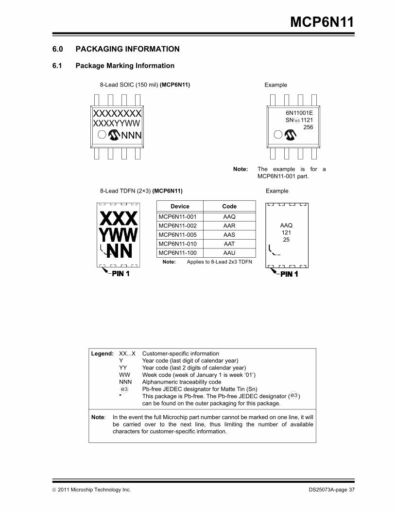
6.0 PACKAGING INFORMATION
6.1 Package Marking Information
Legend: XX...X Customer-specific informationY Year code (last digit of calendar year)YY Year code (last 2 digits of calendar year)WW Week code (week of January 1 is week ‘01’)NNN Alphanumeric traceability code Pb-free JEDEC designator for Matte Tin (Sn)* This package is Pb-free. The Pb-free JEDEC designator ( )
can be found on the outer packaging for this package.
Note: In the event the full Microchip part number cannot be marked on one line, it willbe carried over to the next line, thus limiting the number of availablecharacters for customer-specific information.
3e
3e
8-Lead SOIC (150 mil) (MCP6N11)
8-Lead TDFN (2×3) (MCP6N11) Example
Device Code
MCP6N11-001 AAQMCP6N11-002 AARMCP6N11-005 AASMCP6N11-010 AATMCP6N11-100 AAU
Note: Applies to 8-Lead 2x3 TDFN
Note: The example is for aMCP6N11-001 part.
NNN
6N11001ESN^^ 1121
2563e
AAQ12125
Example
© 2011 Microchip Technology Inc. DS25073A-page 37

MCP6N11
Note: For the most current package drawings, please see the Microchip Packaging Specification located at http://www.microchip.com/packaging
DS25073A-page 38 © 2011 Microchip Technology Inc.

MCP6N11
Note: For the most current package drawings, please see the Microchip Packaging Specification located at http://www.microchip.com/packaging
© 2011 Microchip Technology Inc. DS25073A-page 39

MCP6N11
���������� ��������� �������������������������� ��!�"��#$%
����& ������!"���#�������$����%�&���"'�����"��"���������������(��$�����������)������������%��������*++&&&�!��������!+���$�����
DS25073A-page 40 © 2011 Microchip Technology Inc.

MCP6N11
Note: For the most current package drawings, please see the Microchip Packaging Specification located at http://www.microchip.com/packaging
© 2011 Microchip Technology Inc. DS25073A-page 41

MCP6N11
Note: For the most current package drawings, please see the Microchip Packaging Specification located at http://www.microchip.com/packaging
DS25073A-page 42 © 2011 Microchip Technology Inc.

MCP6N11
���������� ��'���(��������������)�*���+�����,-�-��./���� ��!�"0'(�%
����& ������!"���#�������$����%�&���"'�����"��"���������������(��$�����������)������������%��������*++&&&�!��������!+���$�����
© 2011 Microchip Technology Inc. DS25073A-page 43

MCP6N11
NOTES:DS25073A-page 44 © 2011 Microchip Technology Inc.

MCP6N11
APPENDIX A: REVISION HISTORY
Revision A (October 2011)• Original Release of this Document.
© 2011 Microchip Technology Inc. DS25073A-page 45

MCP6N11
NOTES:DS25073A-page 46 © 2011 Microchip Technology Inc.

MCP6N11
PRODUCT IDENTIFICATION SYSTEMTo order or obtain information, e.g., on pricing or delivery, refer to the factory or the listed sales office.
Device: MCP6N11 Single Instrumentation Amplifier
MCP6N11T Single Instrumentation Amplifier(Tape and Reel)
Gain Option: 001 = Minimum gain of 1 V/V002 = Minimum gain of 2 V/V005 = Minimum gain of 5 V/V010 = Minimum gain of 10 V/V100 = Minimum gain of 100 V/V
Temperature Range: E = -40°C to +125°C
Package: MNY = 2×3 TDFN, 8-lead *SN = Plastic SOIC (150mil Body), 8-lead
* Y = nickel palladium gold manufacturing designator. Onlyavailable on the TDFN package.
Examples:a) MCP6N11T-001E/MNY: Tape and Reel,
Minimum gain = 1,Extended temperature, 8LD 2×3 TDFN.
b) MCP6N11-002E/SN: Minimum gain = 2, Extended temperature,8LD SOIC.
PART NO. –X /XX
PackageGainOption
Device
X
TemperatureRange
© 2011 Microchip Technology Inc. DS25073A-page 47

MCP6N11
NOTES:DS25073A-page 48 © 2011 Microchip Technology Inc.

Note the following details of the code protection feature on Microchip devices:• Microchip products meet the specification contained in their particular Microchip Data Sheet.
• Microchip believes that its family of products is one of the most secure families of its kind on the market today, when used in the intended manner and under normal conditions.
• There are dishonest and possibly illegal methods used to breach the code protection feature. All of these methods, to our knowledge, require using the Microchip products in a manner outside the operating specifications contained in Microchip’s Data Sheets. Most likely, the person doing so is engaged in theft of intellectual property.
• Microchip is willing to work with the customer who is concerned about the integrity of their code.
• Neither Microchip nor any other semiconductor manufacturer can guarantee the security of their code. Code protection does not mean that we are guaranteeing the product as “unbreakable.”
Code protection is constantly evolving. We at Microchip are committed to continuously improving the code protection features of ourproducts. Attempts to break Microchip’s code protection feature may be a violation of the Digital Millennium Copyright Act. If such actsallow unauthorized access to your software or other copyrighted work, you may have a right to sue for relief under that Act.
Information contained in this publication regarding deviceapplications and the like is provided only for your convenienceand may be superseded by updates. It is your responsibility toensure that your application meets with your specifications.MICROCHIP MAKES NO REPRESENTATIONS ORWARRANTIES OF ANY KIND WHETHER EXPRESS ORIMPLIED, WRITTEN OR ORAL, STATUTORY OROTHERWISE, RELATED TO THE INFORMATION,INCLUDING BUT NOT LIMITED TO ITS CONDITION,QUALITY, PERFORMANCE, MERCHANTABILITY ORFITNESS FOR PURPOSE. Microchip disclaims all liabilityarising from this information and its use. Use of Microchipdevices in life support and/or safety applications is entirely atthe buyer’s risk, and the buyer agrees to defend, indemnify andhold harmless Microchip from any and all damages, claims,suits, or expenses resulting from such use. No licenses areconveyed, implicitly or otherwise, under any Microchipintellectual property rights.
© 2011 Microchip Technology Inc.
Trademarks
The Microchip name and logo, the Microchip logo, dsPIC, KEELOQ, KEELOQ logo, MPLAB, PIC, PICmicro, PICSTART, PIC32 logo, rfPIC and UNI/O are registered trademarks of Microchip Technology Incorporated in the U.S.A. and other countries.
FilterLab, Hampshire, HI-TECH C, Linear Active Thermistor, MXDEV, MXLAB, SEEVAL and The Embedded Control Solutions Company are registered trademarks of Microchip Technology Incorporated in the U.S.A.
Analog-for-the-Digital Age, Application Maestro, chipKIT, chipKIT logo, CodeGuard, dsPICDEM, dsPICDEM.net, dsPICworks, dsSPEAK, ECAN, ECONOMONITOR, FanSense, HI-TIDE, In-Circuit Serial Programming, ICSP, Mindi, MiWi, MPASM, MPLAB Certified logo, MPLIB, MPLINK, mTouch, Omniscient Code Generation, PICC, PICC-18, PICDEM, PICDEM.net, PICkit, PICtail, REAL ICE, rfLAB, Select Mode, Total Endurance, TSHARC, UniWinDriver, WiperLock and ZENA are trademarks of Microchip Technology Incorporated in the U.S.A. and other countries.
SQTP is a service mark of Microchip Technology Incorporated in the U.S.A.
All other trademarks mentioned herein are property of their respective companies.
© 2011, Microchip Technology Incorporated, Printed in the U.S.A., All Rights Reserved.
Printed on recycled paper.
ISBN: 978-1-61341-685-3
DS25073A-page 49
Microchip received ISO/TS-16949:2009 certification for its worldwide headquarters, design and wafer fabrication facilities in Chandler and Tempe, Arizona; Gresham, Oregon and design centers in California and India. The Company’s quality system processes and procedures are for its PIC® MCUs and dsPIC® DSCs, KEELOQ® code hopping devices, Serial EEPROMs, microperipherals, nonvolatile memory and analog products. In addition, Microchip’s quality system for the design and manufacture of development systems is ISO 9001:2000 certified.

DS25073A-page 50 © 2011 Microchip Technology Inc.
AMERICASCorporate Office2355 West Chandler Blvd.Chandler, AZ 85224-6199Tel: 480-792-7200 Fax: 480-792-7277Technical Support: http://www.microchip.com/supportWeb Address: www.microchip.comAtlantaDuluth, GA Tel: 678-957-9614 Fax: 678-957-1455BostonWestborough, MA Tel: 774-760-0087 Fax: 774-760-0088ChicagoItasca, IL Tel: 630-285-0071 Fax: 630-285-0075ClevelandIndependence, OH Tel: 216-447-0464 Fax: 216-447-0643DallasAddison, TX Tel: 972-818-7423 Fax: 972-818-2924DetroitFarmington Hills, MI Tel: 248-538-2250Fax: 248-538-2260IndianapolisNoblesville, IN Tel: 317-773-8323Fax: 317-773-5453Los AngelesMission Viejo, CA Tel: 949-462-9523 Fax: 949-462-9608Santa ClaraSanta Clara, CA Tel: 408-961-6444Fax: 408-961-6445TorontoMississauga, Ontario, CanadaTel: 905-673-0699 Fax: 905-673-6509
ASIA/PACIFICAsia Pacific OfficeSuites 3707-14, 37th FloorTower 6, The GatewayHarbour City, KowloonHong KongTel: 852-2401-1200Fax: 852-2401-3431Australia - SydneyTel: 61-2-9868-6733Fax: 61-2-9868-6755China - BeijingTel: 86-10-8569-7000 Fax: 86-10-8528-2104China - ChengduTel: 86-28-8665-5511Fax: 86-28-8665-7889China - ChongqingTel: 86-23-8980-9588Fax: 86-23-8980-9500China - HangzhouTel: 86-571-2819-3187 Fax: 86-571-2819-3189China - Hong Kong SARTel: 852-2401-1200 Fax: 852-2401-3431China - NanjingTel: 86-25-8473-2460Fax: 86-25-8473-2470China - QingdaoTel: 86-532-8502-7355Fax: 86-532-8502-7205China - ShanghaiTel: 86-21-5407-5533 Fax: 86-21-5407-5066China - ShenyangTel: 86-24-2334-2829Fax: 86-24-2334-2393China - ShenzhenTel: 86-755-8203-2660 Fax: 86-755-8203-1760China - WuhanTel: 86-27-5980-5300Fax: 86-27-5980-5118China - XianTel: 86-29-8833-7252Fax: 86-29-8833-7256China - XiamenTel: 86-592-2388138 Fax: 86-592-2388130China - ZhuhaiTel: 86-756-3210040 Fax: 86-756-3210049
ASIA/PACIFICIndia - BangaloreTel: 91-80-3090-4444 Fax: 91-80-3090-4123India - New DelhiTel: 91-11-4160-8631Fax: 91-11-4160-8632India - PuneTel: 91-20-2566-1512Fax: 91-20-2566-1513Japan - YokohamaTel: 81-45-471- 6166 Fax: 81-45-471-6122Korea - DaeguTel: 82-53-744-4301Fax: 82-53-744-4302Korea - SeoulTel: 82-2-554-7200Fax: 82-2-558-5932 or 82-2-558-5934Malaysia - Kuala LumpurTel: 60-3-6201-9857Fax: 60-3-6201-9859Malaysia - PenangTel: 60-4-227-8870Fax: 60-4-227-4068Philippines - ManilaTel: 63-2-634-9065Fax: 63-2-634-9069SingaporeTel: 65-6334-8870Fax: 65-6334-8850Taiwan - Hsin ChuTel: 886-3-5778-366Fax: 886-3-5770-955Taiwan - KaohsiungTel: 886-7-536-4818Fax: 886-7-330-9305Taiwan - TaipeiTel: 886-2-2500-6610 Fax: 886-2-2508-0102Thailand - BangkokTel: 66-2-694-1351Fax: 66-2-694-1350
EUROPEAustria - WelsTel: 43-7242-2244-39Fax: 43-7242-2244-393Denmark - CopenhagenTel: 45-4450-2828 Fax: 45-4485-2829France - ParisTel: 33-1-69-53-63-20 Fax: 33-1-69-30-90-79Germany - MunichTel: 49-89-627-144-0 Fax: 49-89-627-144-44Italy - Milan Tel: 39-0331-742611 Fax: 39-0331-466781Netherlands - DrunenTel: 31-416-690399 Fax: 31-416-690340Spain - MadridTel: 34-91-708-08-90Fax: 34-91-708-08-91UK - WokinghamTel: 44-118-921-5869Fax: 44-118-921-5820
Worldwide Sales and Service
08/02/11