Embed Size (px)
Citation preview
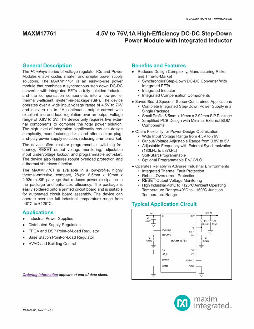
General DescriptionThe Himalaya series of voltage regulator ICs and Power Modules enable cooler, smaller, and simpler power supply solutions. The MAXM17761 is an easy-to-use power module that combines a synchronous step down DC-DC converter with integrated FETs ,a fully shielded inductor, and the compensation components into a low-profile, thermally-efficient, system-in-package (SiP). The device operates over a wide input voltage range of 4.5V to 76V and delivers up to 1A continuous output current with excellent line and load regulation over an output voltage range of 0.8V to 5V. The device only requires five exter-nal components to complete the total power solution. The high level of integration significantly reduces design complexity, manufacturing risks, and offers a true plug-and-play power supply solution, reducing time-to-market.The device offers resistor programmable switching fre-quency, RESET output voltage monitoring, adjustable input undervoltage lockout and programmable soft-start. The device also features robust overload protection and a thermal shutdown function.The MAXM17761 is available in a low-profile, highly thermal-emissive, compact, 28-pin 6.5mm x 10mm x 2.92mm SiP package that reduces power dissipation in the package and enhances efficiency. The package is easily soldered onto a printed circuit board and is suitable for automated circuit board assembly. The device can operate over the full industrial temperature range from -40°C to +125°C.
Applications Industrial Power Supplies Distributed Supply Regulation FPGA and DSP Point-of-Load Regulator Base Station Point-of-Load Regulator HVAC and Building Control
Ordering Information appears at end of data sheet.
19-100085; Rev 1; 9/17
Benefits and Features Reduces Design Complexity, Manufacturing Risks,
and Time-to-Market• Synchronous Step-Down DC-DC Converter With
Integrated FETs• Integrated Inductor• Integrated Compensation Components
Saves Board Space in Space-Constrained Applications• Complete Integrated Step-Down Power Supply in a
Single Package• Small Profile 6.5mm x 10mm x 2.92mm SiP Package• Simplified PCB Design with Minimal External BOM
Components Offers Flexibility for Power-Design Optimization
• Wide Input Voltage Range from 4.5V to 76V• Output-Voltage Adjustable Range from 0.8V to 5V• Adjustable Frequency with External Synchronization
(180kHz to 537kHz)• Soft-Start Programmable• Optional Programmable EN/UVLO
Operates Reliably in Adverse Industrial Environments• Integrated Thermal Fault Protection• Robust Overcurrent Protection• RESET Output Voltage Monitoring• High Industrial -40°C to +125°C Ambient Operating
Temperature Range/-40°C to +150°C Junction Temperature Range
Typical Application Circuit
EN/UVLO
EXTVCC
RT/SYNC
FB
VCC
IN
PGND
OUT3.3V,1A
MAXM17761
C12.2µF R1
69.8kΩ
SGND
C2100µF
VIN
SS
RESET
LX
R2105kΩ
SS_C
FB_RILIM
R3243kΩ
MAXM17761 4.5V to 76V,1A High-Efficiency DC-DC Step-Down Power Module with Integrated Inductor
EVALUATION KIT AVAILABLE
IN to SGND ...........................................................-0.3V to +80VLX to PGND.................................................. -0.3V to VIN + 0.3VOUT to PGND (VIN < 6.3V) .......................... -0.3V to VIN + 0.3VOUT to PGND (VIN > 6.3V) ..................................-0.3V to +6.3VEN/UVLO, EXTVCC to SGND ..............................-0.3V to +26VFB, FB_R, RESET, SS, SS_C, VCC,
RT, ILIM to SGND ................................................-0.3V to +6V
PGND to SGND ....................................................-0.3V to +0.3VOperating Temperature Range ......................... -40°C to +125°CJunction Temperature ......................................................+150°CStorage Temperature Range ............................ -55°C to +125°CLead Temperature (soldering, 10s) .................................+250°CSoldering Temperature (reflow) .......................................+250°C
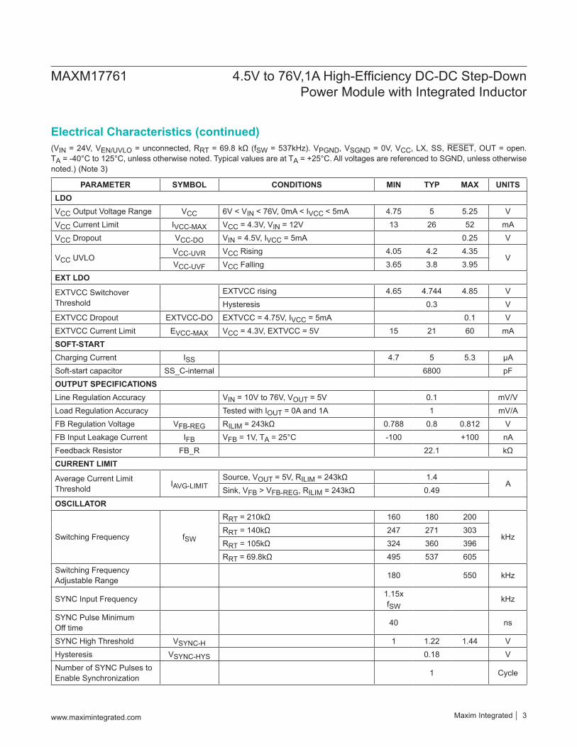
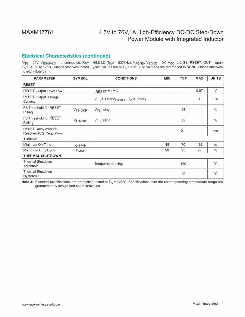
(VIN = 24V, VEN/UVLO = unconnected, RRT = 69.8 kΩ (fSW = 537kHz). VPGND, VSGND = 0V, VCC, LX, SS, RESET, OUT = open. TA = -40°C to 125°C, unless otherwise noted. Typical values are at TA = +25°C. All voltages are referenced to SGND, unless otherwise noted.) (Note 3)
PARAMETER SYMBOL CONDITIONS MIN TYP MAX UNITSINPUT SUPPLYInput Voltage Range VIN 4.5 76 VInput Shut-down Current IIN-SH VEN/UVLO = 0V (shutdown mode) 2.5 5 10 μAInput Quiescent Current IQ-PWM RILIM = 243kΩ 3 4 5 mAEN/UVLO
EN/UVLO ThresholdVENR VEN/UVLO rising 1.19 1.215 1.24
VVENF VEN/UVLO falling 1.09 1.115 1.14VEN-TRUESD VEN/UVLO falling, true shutdown 0.7
Enable Pullup Current IEN VEN/UVLO = 1.215V 2.2 2.5 2.8 μA
Absolute Maximum Ratings (Note 1)
Stresses beyond those listed under “Absolute Maximum Ratings” may cause permanent damage to the device. These are stress ratings only, and functional operation of the device at these or any other conditions beyond those indicated in the operational sections of the specifications is not implied. Exposure to absolute maximum rating conditions for extended periods may affect device reliability.
Note 1: Junction temperature greater than +125°C degrades operating lifetimes.Note 2: Package thermal resistance is measured on evaluation board with natural convection.
PACKAGE TYPE: 28PIN-SiPPackage Code L286510#8Outline Number 21-100181Land Pattern Number 90-100059THERMAL RESISTANCE, FOUR-LAYER BOARD (Note 2)Junction-to-Ambient Thermal Resistance (θJA) 22.5°C/W
For the latest package outline information and land patterns (footprints), go to www.maximintegrated.com/packages. Note that a “+”, “#”, or “-” in the package code indicates RoHS status only. Package drawings may show a different suffix character, but the drawing pertains to the package regardless of RoHS status.
Package Information
Electrical Characteristics
www.maximintegrated.com Maxim Integrated 2
MAXM17761 4.5V to 76V,1A High-Efficiency DC-DC Step-Down Power Module with Integrated Inductor
(VIN = 24V, VEN/UVLO = unconnected, RRT = 69.8 kΩ (fSW = 537kHz). VPGND, VSGND = 0V, VCC, LX, SS, RESET, OUT = open. TA = -40°C to 125°C, unless otherwise noted. Typical values are at TA = +25°C. All voltages are referenced to SGND, unless otherwise noted.) (Note 3)
PARAMETER SYMBOL CONDITIONS MIN TYP MAX UNITSLDOVCC Output Voltage Range VCC 6V < VIN < 76V, 0mA < IVCC < 5mA 4.75 5 5.25 VVCC Current Limit IVCC-MAX VCC = 4.3V, VIN = 12V 13 26 52 mAVCC Dropout VCC-DO VIN = 4.5V, IVCC = 5mA 0.25 V
VCC UVLOVCC-UVR VCC Rising 4.05 4.2 4.35
VVCC-UVF VCC Falling 3.65 3.8 3.95
EXT LDO
EXTVCC Switchover Threshold
EXTVCC rising 4.65 4.744 4.85 VHysteresis 0.3 V
EXTVCC Dropout EXTVCC-DO EXTVCC = 4.75V, IVCC = 5mA 0.1 VEXTVCC Current Limit EVCC-MAX VCC = 4.3V, EXTVCC = 5V 15 21 60 mASOFT-STARTCharging Current ISS 4.7 5 5.3 μASoft-start capacitor SS_C-internal 6800 pFOUTPUT SPECIFICATIONSLine Regulation Accuracy VIN = 10V to 76V, VOUT = 5V 0.1 mV/VLoad Regulation Accuracy Tested with IOUT = 0A and 1A 1 mV/AFB Regulation Voltage VFB-REG RILIM = 243kΩ 0.788 0.8 0.812 VFB Input Leakage Current IFB VFB = 1V, TA = 25°C -100 +100 nAFeedback Resistor FB_R 22.1 kΩCURRENT LIMIT
Average Current Limit Threshold IAVG-LIMIT
Source, VOUT = 5V, RILIM = 243kΩ 1.4A
Sink, VFB > VFB-REG, RILIM = 243kΩ 0.49OSCILLATOR
Switching Frequency fSW
RRT = 210kΩ 160 180 200
kHzRRT = 140kΩ 247 271 303RRT = 105kΩ 324 360 396RRT = 69.8kΩ 495 537 605
Switching Frequency Adjustable Range 180 550 kHz
SYNC Input Frequency 1.15x fSW
kHz
SYNC Pulse Minimum Off time 40 ns
SYNC High Threshold VSYNC-H 1 1.22 1.44 VHysteresis VSYNC-HYS 0.18 VNumber of SYNC Pulses to Enable Synchronization 1 Cycle
Electrical Characteristics (continued)
www.maximintegrated.com Maxim Integrated 3
MAXM17761 4.5V to 76V,1A High-Efficiency DC-DC Step-Down Power Module with Integrated Inductor
Note 3: Electrical specifications are production tested at TA = +25°C. Specifications over the entire operating temperature range are guaranteed by design and characterization.
(VIN = 24V, VEN/UVLO = unconnected, RRT = 69.8 kΩ (fSW = 537kHz). VPGND, VSGND = 0V, VCC, LX, SS, RESET, OUT = open. TA = -40°C to 125°C, unless otherwise noted. Typical values are at TA = +25°C. All voltages are referenced to SGND, unless otherwise noted.) (Note 3)
PARAMETER SYMBOL CONDITIONS MIN TYP MAX UNITS
RESET
RESET Output Level Low IRESET = 1mA 0.07 V
RESET Output leakage Current
VFB = 1.01xVFB-REG, TA = +25°C 1 μA
FB Threshold for RESET Rising
VFB-OKR VFB rising 95 %
FB Threshold for RESET Falling
VFB-OKF VFB falling 92 %
RESET Delay After FB Reaches 95% Regulation
2.1 ms
TIMINGSMinimum On-Time tON-MIN 45 70 115 nsMaximum Duty Cycle DMAX 90 93 97 %THERMAL SHUTDOWNThermal Shutdown Threshold Temperature rising 160 °C
Thermal Shutdown Hysteresis 20 °C
Electrical Characteristics (continued)
www.maximintegrated.com Maxim Integrated 4
MAXM17761 4.5V to 76V,1A High-Efficiency DC-DC Step-Down Power Module with Integrated Inductor
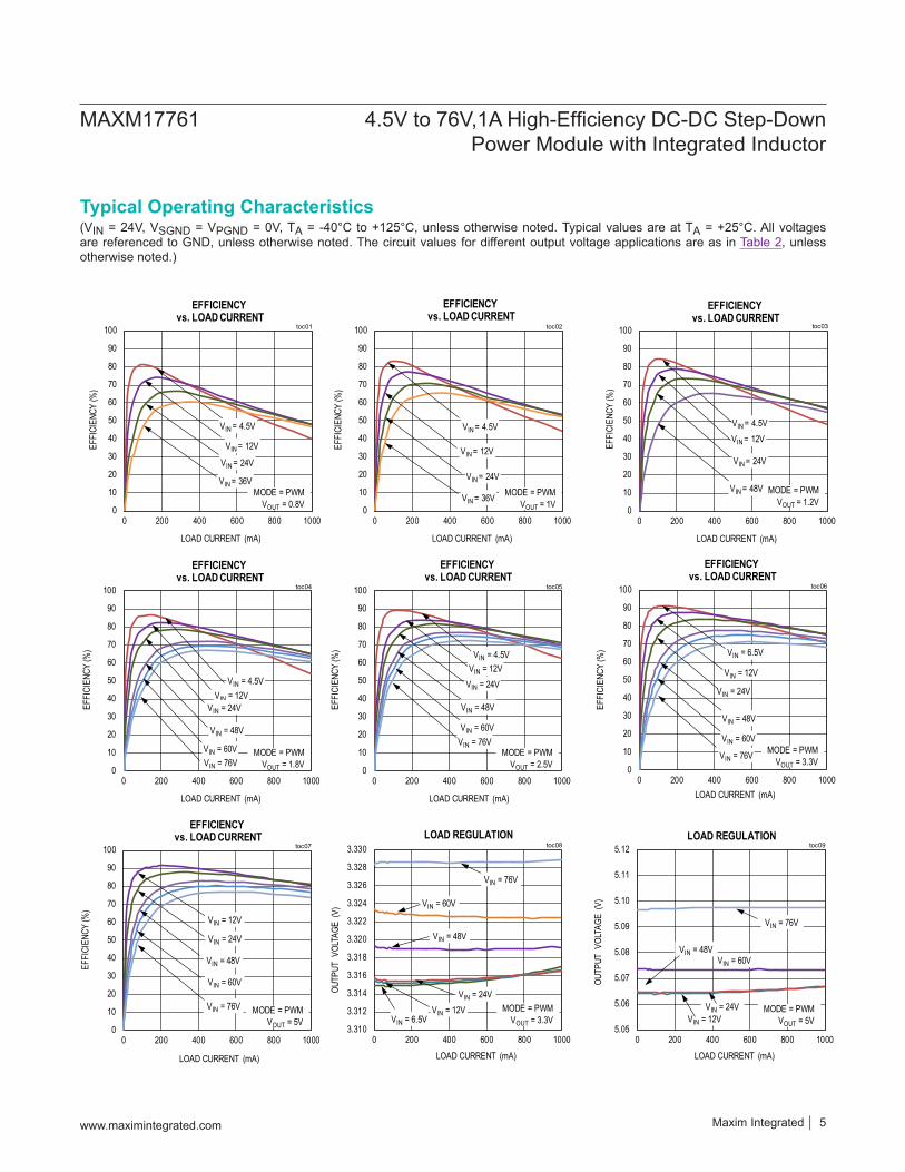
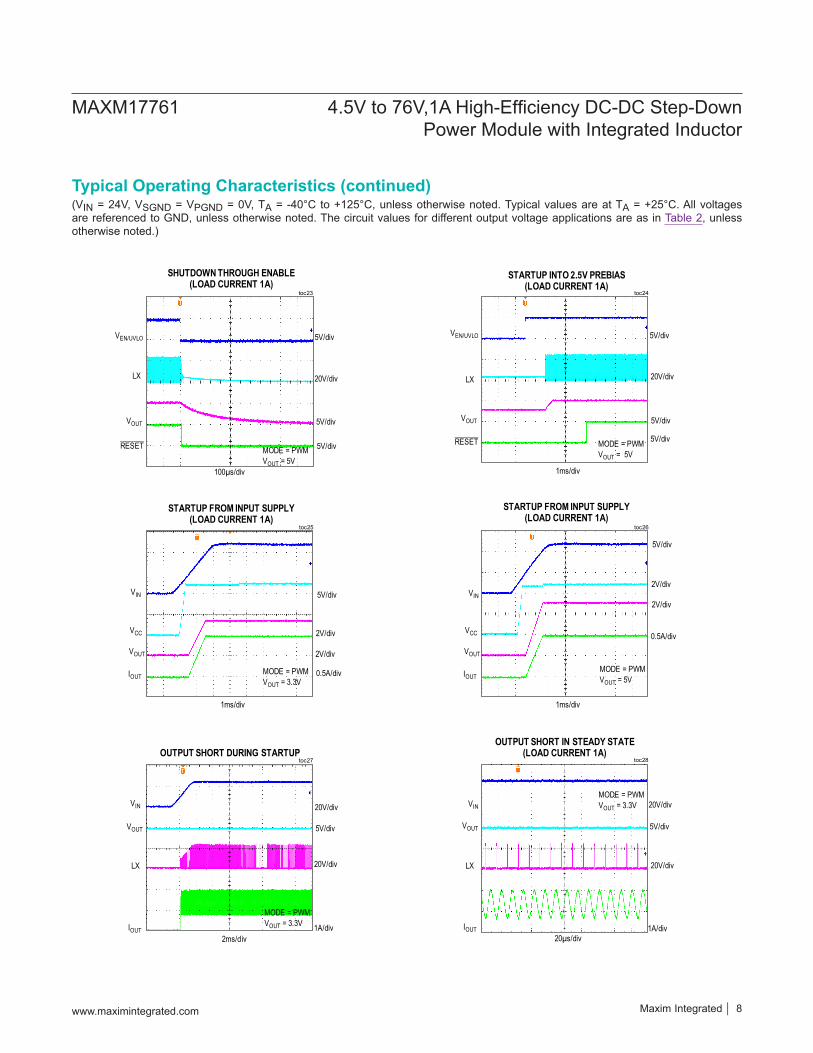
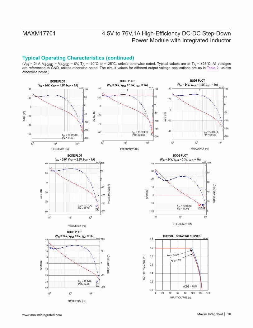
(VIN = 24V, VSGND = VPGND = 0V, TA = -40°C to +125°C, unless otherwise noted. Typical values are at TA = +25°C. All voltages are referenced to GND, unless otherwise noted. The circuit values for different output voltage applications are as in Table 2, unless otherwise noted.)
Typical Operating Characteristics
0
10
20
30
40
50
60
70
80
90
100
0 200 400 600 800 1000
EFFI
CIEN
CY(%
)
LOAD CURRENT (mA)
EFFICIENCY vs. LOAD CURRENT
toc01
VIN = 36V
VIN = 24V
MODE = PWMVOUT = 0.8V
VIN = 12V
VIN = 4.5V
0
10
20
30
40
50
60
70
80
90
100
0 200 400 600 800 1000
EFFI
CIEN
CY(%
)
LOAD CURRENT (mA)
EFFICIENCY vs. LOAD CURRENT
toc04
VIN = 4.5V
MODE = PWMVOUT = 1.8V
VIN = 12VVIN = 24V
VIN = 48V
VIN = 60V
VIN = 76V
0
10
20
30
40
50
60
70
80
90
100
0 200 400 600 800 1000
EFFI
CIEN
CY(%
)
LOAD CURRENT (mA)
EFFICIENCY vs. LOAD CURRENT
toc07
VIN = 24V
VIN = 12V
VIN = 48V
VIN = 60V
MODE = PWMVOUT = 5V
VIN = 76V
0
10
20
30
40
50
60
70
80
90
100
0 200 400 600 800 1000
EFFI
CIEN
CY(%
)
LOAD CURRENT (mA)
EFFICIENCY vs. LOAD CURRENT
toc02
VIN = 36V
VIN = 12V
VIN = 24V
MODE = PWMVOUT = 1V
VIN = 4.5V
0
10
20
30
40
50
60
70
80
90
100
0 200 400 600 800 1000
EFFI
CIEN
CY(%
)
LOAD CURRENT (mA)
EFFICIENCY vs. LOAD CURRENT
toc05
VIN = 24V
VIN = 12V
VIN = 48V
VIN = 60V
MODE = PWMVOUT = 2.5V
VIN = 76V
VIN = 4.5V
3.310
3.312
3.314
3.316
3.318
3.320
3.322
3.324
3.326
3.328
3.330
0 200 400 600 800 1000
OUT
PUT
VO
LTAG
E (V
)
LOAD CURRENT (mA)
LOAD REGULATIONtoc08
VIN = 6.5V
VIN = 60V
VIN = 48V
VIN = 24V
VIN = 12V
VIN = 76V
MODE = PWMVOUT = 3.3V
0
10
20
30
40
50
60
70
80
90
100
0 200 400 600 800 1000
EFFI
CIEN
CY(%
)
LOAD CURRENT (mA)
EFFICIENCY vs. LOAD CURRENT
toc03
VIN = 4.5V
VIN = 12V
MODE = PWMVOUT = 1.2V
VIN = 48V
VIN = 24V
0
10
20
30
40
50
60
70
80
90
100
0 200 400 600 800 1000
EFFI
CIEN
CY(%
)
LOAD CURRENT (mA)
EFFICIENCY vs. LOAD CURRENT
toc06
VIN = 24V
VIN = 6.5V
VIN = 12V
VIN = 48V
VIN = 60VMODE = PWM
VOUT = 3.3VVIN = 76V
5.05
5.06
5.07
5.08
5.09
5.10
5.11
5.12
0 200 400 600 800 1000
OUT
PUT
VO
LTAG
E (V
)
LOAD CURRENT (mA)
LOAD REGULATIONtoc09
VIN = 48V
VIN = 12V
VIN = 76V
MODE = PWMVOUT = 5V
VIN = 60V
VIN = 24V
Maxim Integrated 5www.maximintegrated.com
MAXM17761 4.5V to 76V,1A High-Efficiency DC-DC Step-Down Power Module with Integrated Inductor
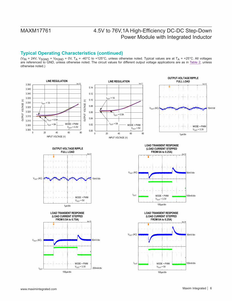
(VIN = 24V, VSGND = VPGND = 0V, TA = -40°C to +125°C, unless otherwise noted. Typical values are at TA = +25°C. All voltages are referenced to GND, unless otherwise noted. The circuit values for different output voltage applications are as in Table 2, unless otherwise noted.)
Typical Operating Characteristics (continued)
3.300
3.305
3.310
3.315
3.320
3.325
3.330
3.335
3.340
3.345
3.350
0 20 40 60 80
OUT
PUT
VO
LTAG
E (V
)
INPUT VOLTAGE (V)
LINE REGULATIONtoc10
IOUT = 0.5A
IOUT = 0A
IOUT = 1A
MODE = PWMVOUT = 3.3V
5.00
5.02
5.04
5.06
5.08
5.10
5.12
5.14
0 20 40 60 80
OUT
PUT
VO
LTAG
E (V
)
INPUT VOLTAGE (V)
LINE REGULATIONtoc11
IOUT = 0.5A
IOUT = 0A
IOUT = 1A
MODE = PWMVOUT = 5V
toc12
1µs/div
VOUT (AC) 10mV/div
OUTPUT-VOLTAGE RIPPLEFULL LOAD
MODE = PWMVOUT = 3.3V
toc13
1µs/div
VOUT (AC) 10mV/div
OUTPUT-VOLTAGE RIPPLEFULL LOAD
MODE = PWMVOUT = 5V
toc14
100µs/div
VOUT (AC) 50mV/div
LOAD TRANSIENT RESPONSE(LOAD CURRENT STEPPED
FROM 0A to 0.25A)
IOUT 100mA/divMODE = PWMVOUT = 3.3V
toc15
100µs/div
VOUT (AC) 50mV/div
LOAD TRANSIENT RESPONSE(LOAD CURRENT STEPPED
FROM 0.5A to 0.75A)
IOUT 200mA/div
MODE = PWMVOUT = 3.3V
toc16
100µs/div
VOUT (AC) 50mV/div
LOAD TRANSIENT RESPONSE(LOAD CURRENT STEPPED
FROM 0A to 0.25A)
IOUT 100mA/divMODE = PWMVOUT = 5V
Maxim Integrated 6www.maximintegrated.com
MAXM17761 4.5V to 76V,1A High-Efficiency DC-DC Step-Down Power Module with Integrated Inductor
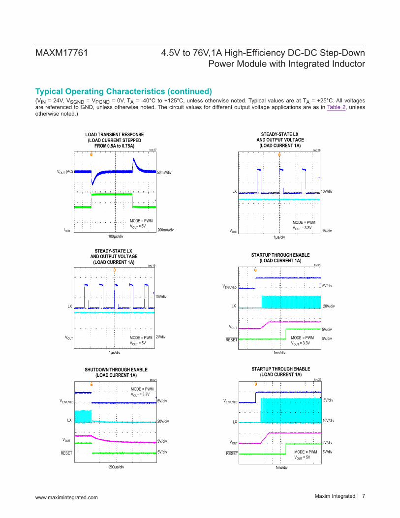
(VIN = 24V, VSGND = VPGND = 0V, TA = -40°C to +125°C, unless otherwise noted. Typical values are at TA = +25°C. All voltages are referenced to GND, unless otherwise noted. The circuit values for different output voltage applications are as in Table 2, unless otherwise noted.)
Typical Operating Characteristics (continued)
toc17
100µs/div
VOUT (AC) 50mV/div
LOAD TRANSIENT RESPONSE(LOAD CURRENT STEPPED
FROM 0.5A to 0.75A)
IOUT 200mA/div
MODE = PWMVOUT = 5V
toc18
1µs/div
VOUT
10V/div
STEADY-STATE LX AND OUTPUT VOLTAGE
(LOAD CURRENT 1A)
LX
1V/div
MODE = PWMVOUT = 3.3V
toc19
1µs/div
VOUT
10V/div
STEADY-STATE LX AND OUTPUT VOLTAGE
(LOAD CURRENT 1A)
LX
2V/divMODE = PWMVOUT = 5V
5V/div
toc20
1ms/div
VEN/UVLO
VOUT
20V/div
5V/div
STARTUP THROUGH ENABLE(LOAD CURRENT 1A)
LX
5V/div
MODE = PWMVOUT = 3.3V
RESET
5V/div
toc21
200µs/div
VEN/UVLO
VOUT
20V/div
5V/div
SHUTDOWN THROUGH ENABLE(LOAD CURRENT 1A)
LX
5V/div
MODE = PWMVOUT = 3.3V
RESET 5V/div
toc22
1ms/div
VEN/UVLO
VOUT
10V/div
5V/div
STARTUP THROUGH ENABLE(LOAD CURRENT 1A)
LX
5V/div
RESET MODE = PWMVOUT = 5V
Maxim Integrated 7www.maximintegrated.com
MAXM17761 4.5V to 76V,1A High-Efficiency DC-DC Step-Down Power Module with Integrated Inductor
(VIN = 24V, VSGND = VPGND = 0V, TA = -40°C to +125°C, unless otherwise noted. Typical values are at TA = +25°C. All voltages are referenced to GND, unless otherwise noted. The circuit values for different output voltage applications are as in Table 2, unless otherwise noted.)
Typical Operating Characteristics (continued)
5V/div
toc23
100µs/div
VEN/UVLO
VOUT
20V/div
5V/div
SHUTDOWN THROUGH ENABLE(LOAD CURRENT 1A)
LX
5V/div
RESET MODE : PWMVOUT=5V
MODE:PWMVOUT = 3.3V
MODE:PWMVOUT = 3.3VMODE = PWM
VOUT = 5V
5V/div
toc24
1ms/div
VEN/UVLO
VOUT
5V/div
20V/div
STARTUP INTO 2.5V PREBIAS(LOAD CURRENT 1A)
LX
5V/div
RESET MODE : PWMVOUT=5V
MODE:PWMVOUT = 5VMODE = PWM
VOUT = 5V
0.5A/div
toc25
1ms/div
VIN
VOUT
5V/div
2V/div
STARTUP FROM INPUT SUPPLY(LOAD CURRENT 1A)
VCC
2V/div
IOUT MODE : PWMVOUT=5V
MODE:PWMVOUT = 5V
MODE = PWMVOUT = 3.3V
0.5A/div
toc26
1ms/div
VIN
VOUT
5V/div
2V/div
STARTUP FROM INPUT SUPPLY(LOAD CURRENT 1A)
VCC
2V/div
IOUT MODE : PWMVOUT=5V
MODE:PWMVOUT = 5VMODE = PWMVOUT = 5V
20V/div
toc27
2ms/div
VIN
VOUT 5V/div
OUTPUT SHORT DURING STARTUP
20V/div
LX
IOUT 1A/div
MODE : PWMVOUT=5V
MODE:PWMVOUT = 3.3V
MODE = PWMVOUT = 3.3V
20V/div
toc28
20µs/div
VOUT 5V/div
OUTPUT SHORT IN STEADY STATE(LOAD CURRENT 1A)
20V/div
LX
VIN
IOUT 1A/div
MODE : PWMVOUT=5V
MODE:PWMVOUT = 3.3V
MODE = PWMVOUT = 3.3V
Maxim Integrated 8www.maximintegrated.com
MAXM17761 4.5V to 76V,1A High-Efficiency DC-DC Step-Down Power Module with Integrated Inductor

(VIN = 24V, VSGND = VPGND = 0V, TA = -40°C to +125°C, unless otherwise noted. Typical values are at TA = +25°C. All voltages are referenced to GND, unless otherwise noted. The circuit values for different output voltage applications are as in Table 2, unless otherwise noted.)
Typical Operating Characteristics (continued)
20V/div
toc29
2ms/div
VIN
VOUT 5V/div
OUTPUT SHORT DURING STARTUP
20V/div
LX
IOUT 1A/div
MODE : PWMVOUT=5V
MODE = PWMVOUT = 5V
20V/div
toc30
20µs/div
VOUT 5V/div
OUTPUT SHORT IN STEADY STATE(LOAD CURRENT 1A)
20V/div
LX
VIN
IOUT 1A/div
2V/div
toc31
20V/div
EXTERNAL SYNCHRONIZATION(LOAD CURRENT 1A)
5V/divSYNC
4µs/div
LX
VOUT MODE : PWMVOUT=5V
MODE = PWMVOUT = 3.3V
2V/div
toc32
20V/div
EXTERNAL SYNCHRONIZATION(LOAD CURRENT = 1A)
5V/div
LX
SYNC
4µs/div
VOUT MODE = PWMVOUT = 5V
1V/div
1V/div
toc33
200µs/div
VOUT
VCC
VCC CHANGEOVER(OUTPUT VOLTAGE = 5V,
LOAD CURRENT = 1A)toc34
FREQUENCY (Hz)
BODE PLOT (VIN = 24V, VOUT = 0.8V, IOUT = 1A
GAI
N (d
B)
PHAS
E M
ARG
IN (°
)
fCR = 14.588kHzPM = 55.313°
40
20
0
-20
-40
-60
-80
200
150
100
50
0
-50
-100
-150
-200
103 104 105
Maxim Integrated 9www.maximintegrated.com
MAXM17761 4.5V to 76V,1A High-Efficiency DC-DC Step-Down Power Module with Integrated Inductor
(VIN = 24V, VSGND = VPGND = 0V, TA = -40°C to +125°C, unless otherwise noted. Typical values are at TA = +25°C. All voltages are referenced to GND, unless otherwise noted. The circuit values for different output voltage applications are as in Table 2, unless otherwise noted.)
Typical Operating Characteristics (continued)
toc37
FREQUENCY (Hz)
GAI
N (d
B)
PHAS
E M
ARG
IN ( °
)
BODE PLOT (VIN = 24V, VOUT = 1.8V, IOUT = 1A)
fCR = 14.59kHzPM = 61.642°
40
20
0
-20
-40
100
50
0
-50
-100
-150
-200
103 104 105
toc38
FREQUENCY (Hz)
GAI
N (d
B)
PHAS
E M
ARG
IN (°
)
BODE PLOT (VIN = 24V, VOUT = 2.5V, IOUT = 1A)
fCR = 14.37kHzPM = 67.72°
40
20
0
-20
-40
-60
100
50
0
-50
-100
-150
-200
103 104 105
toc39
FREQUENCY (Hz)
GAI
N (d
B)
PHAS
E M
ARG
IN (°
)
BODE PLOT (VIN = 24V, VOUT = 3.3V, IOUT = 1A)
fCR = 16.06kHzPM = 71.748°
40
30
20
10
0
-10
-20
100
80
60
40
20
0
103 104 105
toc40
FREQUENCY (Hz)
GAI
N (d
B)
PHAS
E M
ARG
IN (°
)
BODE PLOT (VIN = 24V, VOUT = 5V, IOUT = 1A)
fCR = 22.3kHzPM = 74.28°
40
30
20
10
0
-10
-20
-30
-40
100
50
0
-50
-100
103 104 1050.0
0.2
0.4
0.6
0.8
1.0
1.2
0 20 40 60 80 100 120 140
OUT
PUT
VO
LTAG
E (V
)
INPUT VOLTAGE (V)
THERMAL DERATING CURVEStoc41
VOUT = 3.3V
VOUT = 5V
MODE = PWM
toc35
FREQUENCY (Hz)
BODE PLOT (VIN = 24V, VOUT = 1.2V, IOUT = 1A)
GAI
N (d
B)
PHAS
E M
ARG
IN (°
)40
20
0
-20
-40
-60
100
50
0
-50
-100
-150
-200
103 104 105
fCR = 12.976kHzPM = 61.73°
toc36
BODE PLOT (VIN = 24V, VOUT = 1.5V, IOUT = 1A)
fCR = 13.563kHzPM = 62.058°
FREQUENCY (Hz)
GAI
N (d
B)
PHAS
E M
ARG
IN (°
)
40
20
0
-20
-40
-60
100
50
0
-50
-100
-150
-200
103 104 105
Maxim Integrated 10www.maximintegrated.com
MAXM17761 4.5V to 76V,1A High-Efficiency DC-DC Step-Down Power Module with Integrated Inductor
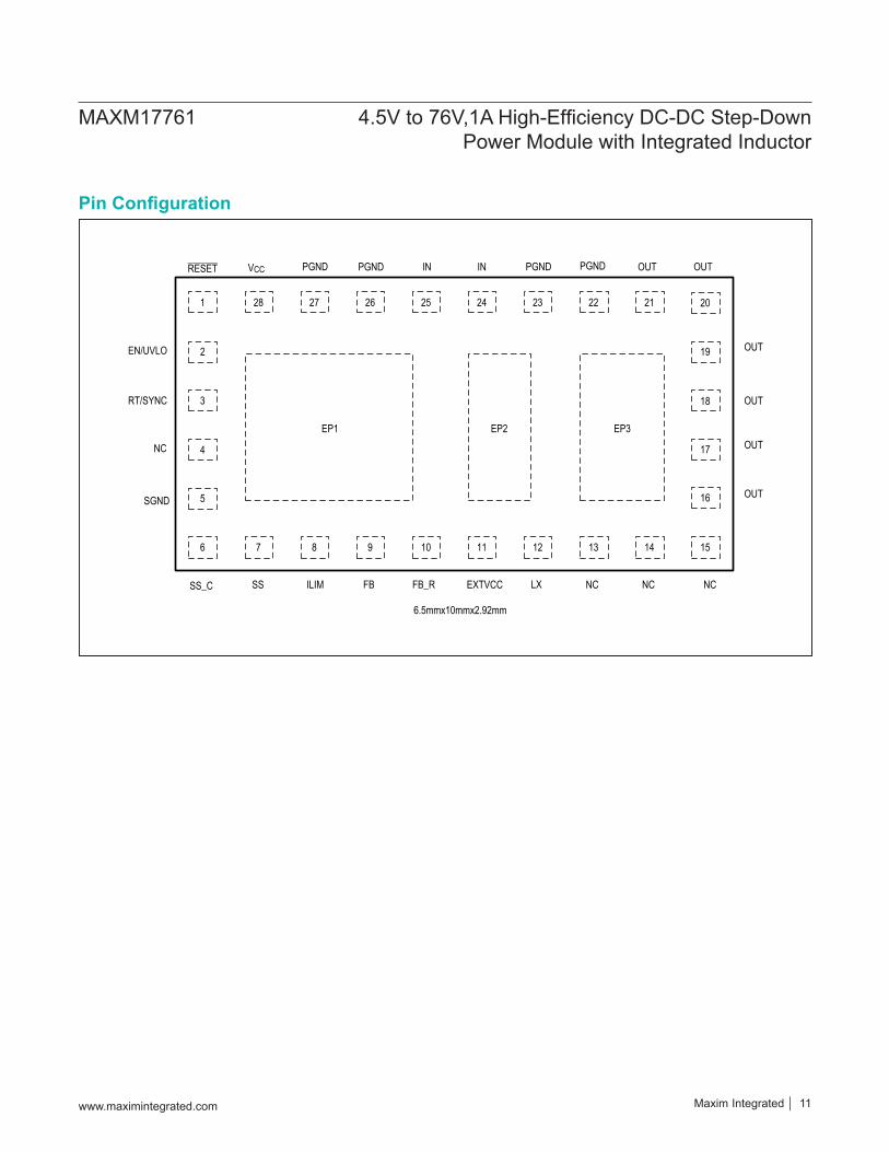
Pin Configuration
1 28 27 25 2426 23 22 21
2
3
4
5
6 7 8 9 11 1210 13 14 15
20
19
18
17
16
EP1 EP2 EP3
6.5mmx10mmx2.92mm
ININPGND OUT OUT
OUT
OUT
OUT
OUT
EN/UVLO
RESET
NC
VCC
SS_C SS ILIM FB FB_R EXTVCC LX NC NC NC
PGND PGND PGND
SGND
RT/SYNC
www.maximintegrated.com Maxim Integrated 11
MAXM17761 4.5V to 76V,1A High-Efficiency DC-DC Step-Down Power Module with Integrated Inductor
PIN NAME FUNCTION
1 RESET Open-Drain RESET Output. The RESET output is driven low if FB drops below 92% of its set value. RESET goes high 2.1ms after FB rises above 95% of its set value.
2 EN/UVLOEnable/Undervoltage Lockout Pin. Drive EN/UVLO high to enable the output. Connect to the center of the resistor-divider between VIN and SGND to set the input voltage at which the part turns on. Leave the pin floating for always on operation.
3 RT/SYNCConnect a resistor from RT to SGND to set the switching frequency of the part between 180kHz and 537kHz. An external pulse can be applied to RT/SYNC through a coupling capacitor to synchronize the internal clock to the external pulse frequency. See the External Synchronization section for details.
4,13-15, EP2 NC No Connection5 SGND Analog Ground Pin
6 SS_C Soft-Start Capacitor. Internally, a 6800pF is connected from SS_C to SGND. Connect this pin to SS to use the internal cap for the soft-start function.
7 SSSoft-Start Input. This module has one internal 6800pF capacitor from the SS_C pin to SGND, which programs a default soft-start time of 1ms when the SS pin is connected to SS_C. If soft-start time needs to be increased, connect an external capacitor from the SS pin to SGND.
8 ILIM Connect a 243kΩ resistor from ILIM to SGND.
9 FBFeedback Input. Internally, a 22.1k is connected between FB_R and SGND. Connect FB pin to FB_R to use the default internal component as a bottom resistor of the feedback resistive divider network. To set the programmable output, connect a resistor from OUT pin to FB.
10 FB_R Feedback Resistive Node. Internally, a 22.1k is connected between FB_R and SGND. Connect this pin to FB to use the resistor as a default bottom resistor in the feeback resistive network.
11 EXTVCC External Input for Powering Control Circuitry From the Output Side. Applying a voltage between 4.84V and 24V at the EXTVCC pin will bypass the internal LDO and improve efficiency.
12 LX Switching Node.Do not connect external components to LX pin.
16-21 OUT Regulator Output. Connect a capacitor from OUT to PGND. See PCB Layout Guidelines for more connection details.
22,23,26,27 PGND Power Ground. Connect the PGND pins externally to the power ground plane
24,25 IN Power-Supply Input. Connect the VIN pins together. Decouple to PGND with a capacitor, place the capacitor close to the VIN and PGND pins.
28 VCC5V LDO Output. The VCC is bypassed to PGND internally through a 2.2µF capacitor. Do not con-nect external components to VCC pin
EP1 SGND Exposed Pad. Connect to the SGND of the Module. Connect a large copper plane below the module to improve the heat dissipation capability.
EP3 OUT Exposed Pad. Connect to the OUT pins of the Module. Connect a large copper plane below the module to improve the heat dissipation capability.
Pin Description
www.maximintegrated.com Maxim Integrated 12
MAXM17761 4.5V to 76V,1A High-Efficiency DC-DC Step-Down Power Module with Integrated Inductor
PEAK CURRENT-MODE
CONTROLLER
VCC
SGND
EN/UVLO
RT/SYNC
SS
OUT
PGND
RESETFB
RESETLogic
LDO
OSCILLATOR
1µF
0.1µF
2.2uF
1.215V
MAXM17761
22µH
SS_C
6800pF
FB
EXTVCC
VCC_INT
IN
LX
4.7Ω
0.1µF
ILIM
FB_R22.1kΩ
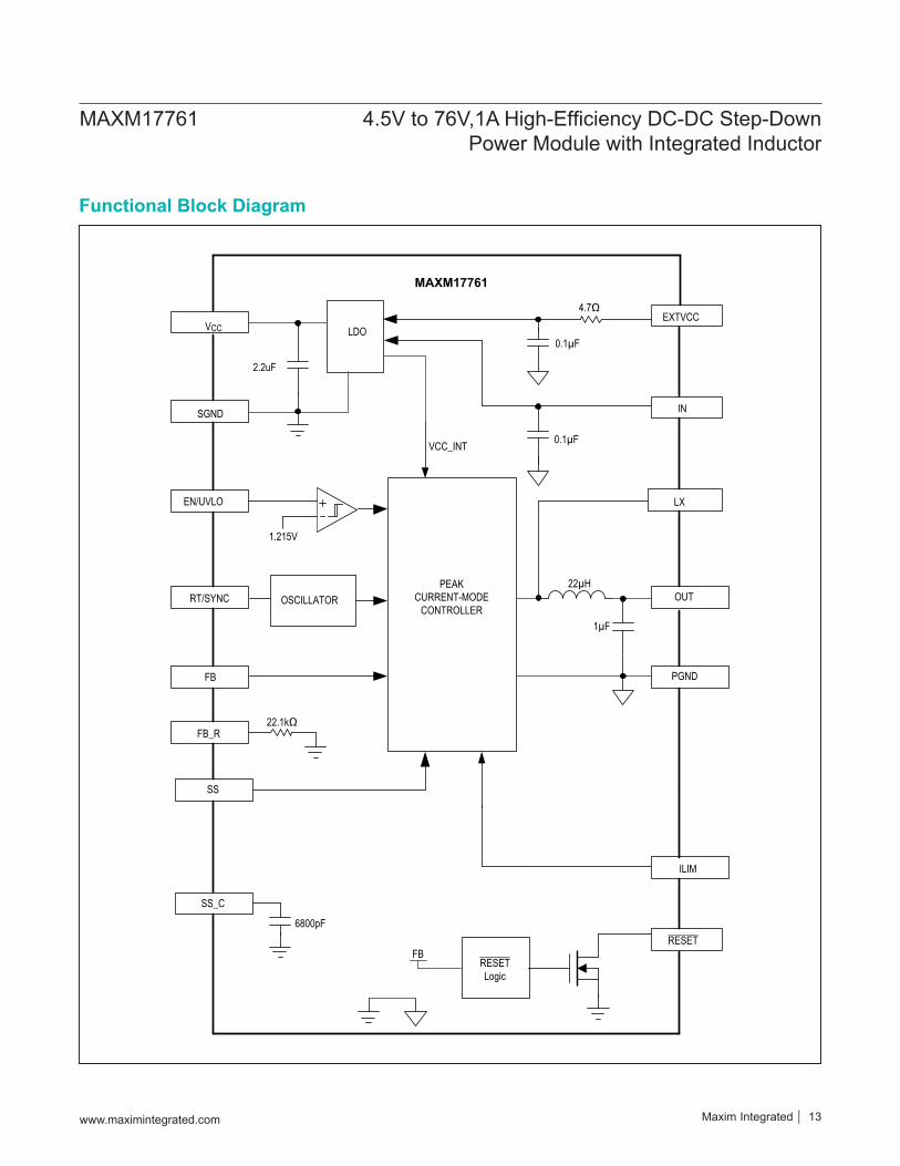
Functional Block Diagram
www.maximintegrated.com Maxim Integrated 13
MAXM17761 4.5V to 76V,1A High-Efficiency DC-DC Step-Down Power Module with Integrated Inductor
Detailed DescriptionThe MAXM17761 is a high-efficiency, high voltage step-down power module with dual integrated MOSFETs that operate over a 4.5V to 76V input supports a programmable output voltage from 0.8V to 5V, delivering up to 1A current. The module integrates all the necessary components required for switching converter. The feedback voltage regulation accuracy meets ±1.5% over load, line, and temperature. The device uses a peak-current-mode control scheme. An internal transconductance error amplifier generates an error voltage. The error voltage sets the duty cycle using a PWM comparator, a high-side current-sense amplifier, and a slope- compensation generator.At each rising-edge of the clock, the high-side pMOSFET turns on, and remains on, until either the appropriate or maximum duty cycle is reached, or the peak current limit is detected. During the high-side MOSFET’s on-time, the inductor current ramps up. During the second-half of the switching cycle, the high-side MOSFET turns off and the low-side nMOSFET turns on and remains on until either the next rising edge of the clock arrives or sink current limit is detected. The inductor releases the stored energy as its current ramps down, and provides current to the RDS(ON) pMOS/nMOS switches ensure high efficiency at full load. This device also integrates a switching frequency selector pin, current limit pin, enable/undervoltage lockout (EN/UVLO) pin, programmable soft-start pin, and open-drain RESET signal.
Mode of OperationThe MAXM17761 operates in PWM Mode. In PWM mode, the inductor current is allowed to go negative. PWM operation provides constant frequency operation at all loads, and is useful in applications sensitive to variable switching frequency.
Switching Frequency Selection and External Frequency SynchronizationThe RT/SYNC pin programs the switching frequency of the converter. Connect a resistor from RT/SYNC to SGND to set the switching frequency of the part at any one of four discrete frequencies—180kHz, 271kHZ, 360kHz, and 537kHz. Table 1 provides resistor values.The device can be synchronized by an external clock signal on the RT/SYNC pin. The external clock should
be coupled to the RT/SYNC pin through a 47pF capacitor, as shown in Figure 1. The external synchronization clock frequency must be between 1.15 x fSW and 1.4 x fSW, where fSW is the frequency programmed by the RT resis-tor. When an external clock is applied to the RT/SYNC pin, the internal oscillator frequency changes to external clock frequency from original frequency base on RT set-tings. The minimum external clock pulse-width low should be greater than 40ns. See the Oscillator section of the Electrical Characteristics table for details. Connect the SYNC pin to SGND if it is not used.
Linear RegulatorThe MAXM17761 has two internal LDO (Low Dropout) regulators which powers VCC. One LDO is powered from VIN (INLDO) and the other LDO is powered from EXTVCC (EXTVCC LDO). During power-up, when Enable pin voltage is above the true shutdown voltage , then the VCC is powered from INLDO. When VCC voltage is above the VCC UVLO threshold and the EXTVCC voltage is greater than 4.74V(typ), then the VCC is powered from EXTVCC LDO. Only one of the two LDOs is in operation at a time, depending on the voltage levels present at EXTVCC. Powering VCC from EXTVCC increases efficiency at higher input voltages. EXTVCC voltage should not exceed 26V.
Table 1. Setting the Switching FrequencySWITCHING FREQUENCY
(KHZ) RT/SYNC RESISTOR (KΩ)
180 210271 140360 105537 69.8
Figure 1. External Frequency Synchronization
MAXM17761
RT/SYNC
SGND
RRT
47pF
CLOCKSOURCE
www.maximintegrated.com Maxim Integrated 14
MAXM17761 4.5V to 76V,1A High-Efficiency DC-DC Step-Down Power Module with Integrated Inductor
Note: The X5R capacitors are selected as output capacitors in this table for different applications. In applications where the X7R capacitor is needed, follow the procedure given in the Output Capacitor Selection section to select the suitable capacitor.
Operating Input Voltage RangeThe maximum input voltage is determined by the mini-mum controllable on-time, while the minimum input volt-age is determined by the maximum duty cycle and the circuit-voltage drops. The minimum and maximum operat-ing input voltages for a given output voltage should satisfy the following conditions:
( ) ( )OUT OUT(MAX)IN(MIN) OUT(MAX)
MAX
V I 0.913V I 1.25
D
+ ×≥ + ×
SWIN(MIN) OUT
OUTIN(MAX)
SW(MAX) ON(MIN)
fFor Duty Cycle, D 0.3 : V 4.25 V46.5
VVf t
> ≥ × −
≤×
where: VOUT = Steady-state output voltage IOUT(MAX) = Maximum load currentDMAX = Maximum allowable duty ratio fSW(MAX) = Maximum switching frequencytON(MIN) = Worst-case minimum switch on-time (115ns)Table 2 provides operating input-voltage ranges and the optimum switching frequency for different selected output voltages.
RESET OutputThe device includes a RESET pin to monitor the output voltage. The open-drain RESET output requires an external pullup resistor. RESET goes high (high impedance) 2.1ms after the output voltage increases above 95% of the nominal voltage. RESET goes low when the output voltage drops to below 92% of the nominal voltage. RESET also goes low during thermal shutdown.
Overcurrent ProtectionThe device is provided with a robust overcurrent protection scheme that protects the device under overload and output short-circuit conditions. When the overcurrent occurs, the module enters into hysteretic mode and limits the average output current delivered. Also, the module limits the average sink current by turning off the low-side switch in the event of negative over current.
Thermal Shutdown ProtectionThermal shutdown protection limits total power dissipation in the device. When the junction temperature of the device exceeds +160°C, an on-chip thermal sensor shuts down the device, allowing the device to cool. The thermal sensor turns the device on again after the junction temperature cools by 20°C. Soft-start resets during thermal shutdown. Carefully evaluate the total power dissipation to avoid unwanted triggering of the thermal shutdown protection in normal operation.
Table 2. Selection Of Component ValuesVINMIN (V) VINMAX (V) VOUT (V) CIN (µF) COUT (µF) (Note 2) RU (KΩ) fSW (KHZ) RT (KΩ)
4.5 36 0.8 4x2.2 100V 1206 3x100 6.3V 1210 0 180 210
4.5 40 1 4x2.2 100V 1206 2x100 6.3V 1210 +1x47 6.3V 1210 5.62 180 210
4.5 60 1.2 4x2.2 100V 1206 2x100 6.3V 1210 +1x22 6.3V 1210 11 180 210
4.5 60 1.5 3x2.2 100V 1206 2x100 6.3V 1210 19.6 180 210
4.5 76 1.8 3x2.2 100V 1206 1x100 6.3V 1210 +1x47 6.3V 1210 28 180 210
5 76 2.5 2x2.2 100V 1206 1x100 6.3V 1210 +1x22 6.3V 1210 47 271 140
6.5 76 3.3 1x2.2 100V 1206 1x100 6.3V 1210 69.8 360 10510 76 5 1x2.2 100V 1206 1x47 10V 1210 118 537 69.8
www.maximintegrated.com Maxim Integrated 15
MAXM17761 4.5V to 76V,1A High-Efficiency DC-DC Step-Down Power Module with Integrated Inductor
Applications InformationInput Capacitor SelectionThe input filter capacitor reduces peak currents drawn from the power source and reduces noise and voltage ripple on the input caused by the circuit’s switching. The input capacitor RMS current requirement (IRMS) for a single output is defined by the following equation:
IRMS = IOUT(MAX) ×√(VOUT × (VIN − VOUT))
VINwhere, IOUT(MAX) is the maximum load current. IRMS has a maximum value when the input voltage equals twice the output voltage (VIN = 2 x VOUT), so IRMS(MAX) = IOUT(MAX)/2.Choose an input capacitor that exhibits less than +10°C temperature rise at the RMS input current for optimal long term reliability. Use low-ESR ceramic capacitors with high ripple-current capability at the input. X7R capacitors are recommended in industrial applications for their temperature stability. Calculate the input capacitance using the following equation:
CIN =IOUT(MAX) × D × (1 − D)
η × fSW × ΔVIN
where D = VOUT/VIN is the duty ratio of the controller, fSW is the switching frequency, ΔVIN is the allowable input voltage ripple, and η is the efficiency. In applications where the source is located distant from the device input, an electrolytic capacitor should be added in parallel to the ceramic capacitor to provide necessary damping for potential oscillations caused by the inductance of the longer input power path and input ceramic capacitor.
Output Capacitor SelectionCeramic output capacitors are preferred due to their stabil-ity over temperature in industrial applications. In Table 2, the output capacitor is sized to support a step load of 25%
of the maximum output current in the application, such that the output-voltage deviation is contained to 3% of the output voltage. The minimum value of output capacitance required can be calculated using the following equations:
OUT SWOUT
200C F; if f 180kHzV
= µ =
OUT SWOUT
and150C F; if f is other than 180kHz
V= µ
Derating of ceramic capacitors with DC voltage must be considered while selecting the output capacitor. Derating curves are available from all major ceramic capacitor vendors.
Soft-Start Capacitor SelectionThe device implements an adjustable soft-start operation to reduce inrush current during startup.Internally, a 6800pF is connected from SS_C to SGND. Connect this pin to SS to use the internal capacitor for the soft-start programming. An additional (CSS) connected from the SS pin to SGND can be used to program the different soft-start time. The selected output capacitance (CSEL) and the output voltage (VOUT) determine the minimum value of CSS, as shown by the following equation.
CSS ≥ 30 × 10−6 × CSEL × VOUT
The soft-start time (tSS) is related to the capacitor connected at SS (CSS) by the following equation.
tSS =CSS
6.25 × 10⁻⁶
For example, to program a 2ms soft-start time, a 12nF capacitor should be connected from the SS pin to SGND.
www.maximintegrated.com Maxim Integrated 16
MAXM17761 4.5V to 76V,1A High-Efficiency DC-DC Step-Down Power Module with Integrated Inductor
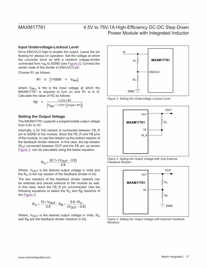
Input Undervoltage-Lockout LevelDrive EN/UVLO high to enable the output. Leave the pin floating for always on operation. Set the voltage at which the converter turns on with a resistive voltage-divider connected from VIN to SGND (see Figure 2). Connect the center node of the divider to EN/UVLO pin.Choose R1 as follows:
R1 ≤ (110000 × VINU)where VINU is the is the input voltage at which the MAXM17761 is required to turn on and R1 is in Ω. Calculate the value of R2 as follows:
R2 = 1.215 × R1
(VINU − 1.215 + (2.5μA × R1))
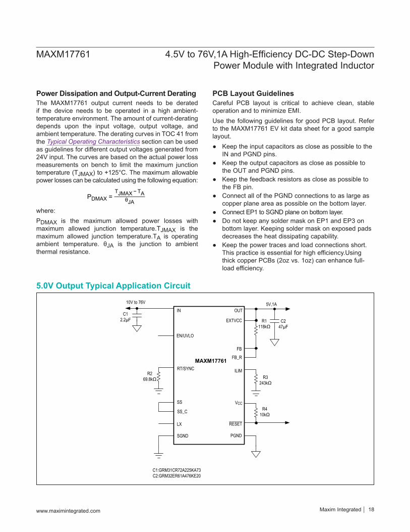
Setting the Output VoltageThe MAXM17761 supports a programmable output voltage from 0.8V to 5V. Internally, a 22.1kΩ resistor is connected between FB_R pin to SGND of the module. Short the FB_R and FB pins of the module, to use this resistor as the bottom resistor of the feedback divider network. In this case, the top resistor (RU) connected between OUT and the FB pin, as shown Figure 3, can be calculated using the below equation,
OUTU
22.1 (V 0.8)R0.8
× −=
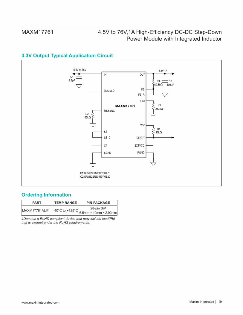
Where, VOUT is the desired output voltage in Volts and the RU is the top resistor of the feedback divider in kΩ.The two resistors of the feedback divider network can be selected and placed external to the module as well. In this case, leave the FB_R pin unconnected. Use the following equations to select the RU and RB resistors of the Figure 4.
OUT UU B
OUT
15 V 0.8 RR ; R0.8 (V 0.8)× ×
= =−
Where, VOUT is the desired output voltage in Volts, RU and RB are the feedback divider resistors in kΩ.
Figure 2. Setting the Undervoltage Lockout Level
Figure 3. Setting the Output Voltage with One External Feedback Resistor
Figure 4. Setting the Output Voltage with External Feedback Resistors
MAXM17761
EN/UVLO
IN
SGND
R1
R2
FB
VOUTOUT
FB_R
RUMAXM17761
RU
RB
MAXM17761
FB
VOUT
SGND
OUT
www.maximintegrated.com Maxim Integrated 17
MAXM17761 4.5V to 76V,1A High-Efficiency DC-DC Step-Down Power Module with Integrated Inductor
Power Dissipation and Output-Current DeratingThe MAXM17761 output current needs to be derated if the device needs to be operated in a high ambient-temperature environment. The amount of current-derating depends upon the input voltage, output voltage, and ambient temperature. The derating curves in TOC 41 from the Typical Operating Characteristics section can be used as guidelines for different output voltages generated from 24V input. The curves are based on the actual power loss measurements on bench to limit the maximum junction temperature (TJMAX) to +125°C. The maximum allowable power losses can be calculated using the following equation:
PDMAX =TJMAX− TA
θJAwhere:PDMAX is the maximum allowed power losses with maximum allowed junction temperature.TJMAX is the maximum allowed junction temperature.TA is operating ambient temperature. θJA is the junction to ambient thermal resistance.
PCB Layout GuidelinesCareful PCB layout is critical to achieve clean, stable operation and to minimize EMI. Use the following guidelines for good PCB layout. Refer to the MAXM17761 EV kit data sheet for a good sample layout.
Keep the input capacitors as close as possible to the IN and PGND pins.
Keep the output capacitors as close as possible to the OUT and PGND pins.
Keep the feedback resistors as close as possible to the FB pin.
Connect all of the PGND connections to as large as copper plane area as possible on the bottom layer.
Connect EP1 to SGND plane on bottom layer. Do not keep any solder mask on EP1 and EP3 on
bottom layer. Keeping solder mask on exposed pads decreases the heat dissipating capability.
Keep the power traces and load connections short. This practice is essential for high efficiency.Using thick copper PCBs (2oz vs. 1oz) can enhance full-load efficiency.
EXTVCC
RT/SYNC
FB
VCC
IN
PGND
OUT5V,1A
MAXM17761
C12.2µF R1
118kΩ
SGND
C247µF
10V to 76V
SS
RESETLX
R269.8kΩ
SS_C
FB_R
ILIMR3
243kΩ
R410kΩ
C1:GRM31CR72A225KA73C2:GRM32ER61A476KE20
EN/UVLO
5.0V Output Typical Application Circuit
www.maximintegrated.com Maxim Integrated 18
MAXM17761 4.5V to 76V,1A High-Efficiency DC-DC Step-Down Power Module with Integrated Inductor
PART TEMP RANGE PIN-PACKAGE
MAXM17761ALI# -40°C to +125°C 28-pin SiP6.5mm × 10mm × 2.92mm
#Denotes a RoHS-compliant device that may include lead(Pb) that is exempt under the RoHS requirements.
EN/UVLO
EXTVCC
RT/SYNC
FB
VCC
IN
PGND
OUT3.3V,1A
MAXM17761
C12.2µF R1
69.8kΩ
SGND
C2100µF
6.5V to 76V
SS
RESET
LX
R2105kΩ
SS_C
FB_R
ILIMR3
243kΩ
R410kΩ
C1:GRM31CR72A225KA73C2:GRM32ER60J107ME20
3.3V Output Typical Application Circuit
Ordering Information
www.maximintegrated.com Maxim Integrated 19
MAXM17761 4.5V to 76V,1A High-Efficiency DC-DC Step-Down Power Module with Integrated Inductor
REVISIONNUMBER
REVISIONDATE DESCRIPTION PAGES
CHANGED0 6/17 Initial release —
1 9/17
Updated Package Information table, Typical Operating Characteristics global characteristics, and TOC 08-11 and TOC 24. Merged and updated Switching Frequency Selection and External Frequency Synchronization sections, and added captions to Figures 1, 3 and 4, and updated the caption for Figure 2. Updated the Power Dissipation and Output-Current Derating TOC reference to TOC 41, and updated the part number in the Ordering Information table. Replaced the Output Capacitor Selection and Operating Input-Voltage Range sections.
2, 5–10, 14–19
Revision History
Maxim Integrated cannot assume responsibility for use of any circuitry other than circuitry entirely embodied in a Maxim Integrated product. No circuit patent licenses are implied. Maxim Integrated reserves the right to change the circuitry and specifications without notice at any time. The parametric values (min and max limits) shown in the Electrical Characteristics table are guaranteed. Other parametric values quoted in this data sheet are provided for guidance.
Maxim Integrated and the Maxim Integrated logo are trademarks of Maxim Integrated Products, Inc. © 2017 Maxim Integrated Products, Inc. 20
MAXM17761 4.5V to 76V,1A High-Efficiency DC-DC Step-Down Power Module with Integrated Inductor
For pricing, delivery, and ordering information, please contact Maxim Direct at 1-888-629-4642, or visit Maxim Integrated’s website at www.maximintegrated.com.


![· -Manual Tuning -Direct keypad Entry ... TECSUN kHz SYNC USB — PAGE ± FM SW DETECTOR ... PL-660. pow FM] AM] SW VOLUM flashin](https://img.dokumen.tips/doc/110x75/5beae02909d3f2ff498c2863/-manual-tuning-direct-keypad-entry-tecsun-khz-sync-usb-page-fm-sw.jpg)