Embed Size (px)
Citation preview
Lecture 17: Adders
CMOS VLSI DesignCMOS VLSI Design 4th Ed.17: Adders 2
Outline Single-bit Addition Carry-Ripple Adder Carry-Skip Adder Carry-Lookahead Adder Carry-Select Adder Carry-Increment Adder Tree Adder
CMOS VLSI DesignCMOS VLSI Design 4th Ed.17: Adders 3
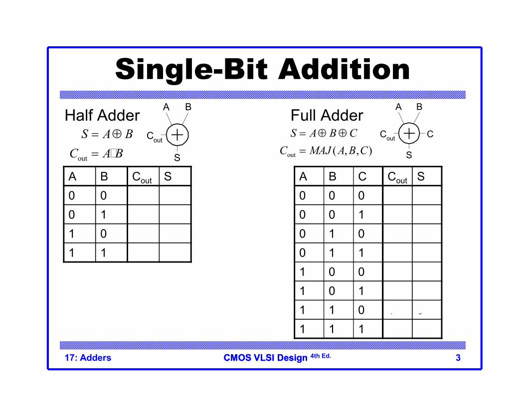
Single-Bit AdditionHalf Adder Full Adder
A B Cout S0 0 0 00 1 0 11 0 0 11 1 1 0
A B C Cout S0 0 0 0 00 0 1 0 10 1 0 0 10 1 1 1 01 0 0 0 11 0 1 1 01 1 0 1 01 1 1 1 1
A B
S
Cout
A B
C
S
Cout
out
S A BC A B
� out ( , , )
S A B CC MAJ A B C

CMOS VLSI DesignCMOS VLSI Design 4th Ed.17: Adders 4
PGK For a full adder, define what happens to carries
(in terms of A and B)– Generate: Cout = 1 independent of C
• G = A • B– Propagate: Cout = C
• P = A B– Kill: Cout = 0 independent of C
• K = ~A • ~B
CMOS VLSI DesignCMOS VLSI Design 4th Ed.17: Adders 5
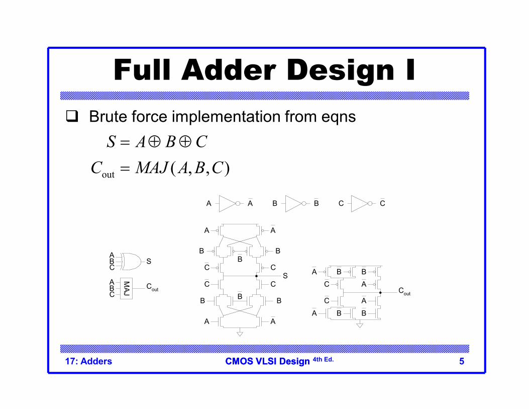
Full Adder Design I Brute force implementation from eqns
out ( , , )S A B C
C MAJ A B C
ABC
S
Cout
MAJ
ABC
A
B BB
A
CS
C
CC
B BB
A A
A B
C
B
A
CBA A B C
Cout
C
A
A
BB

CMOS VLSI DesignCMOS VLSI Design 4th Ed.17: Adders 6
Full Adder Design II Factor S in terms of Cout
S = ABC + (A + B + C)(~Cout) Critical path is usually C to Cout in ripple adder
SS
Cout
A
BC
Cout
MINORITY

CMOS VLSI DesignCMOS VLSI Design 4th Ed.17: Adders 7
Layout Clever layout circumvents usual line of diffusion
– Use wide transistors on critical path– Eliminate output inverters
CMOS VLSI DesignCMOS VLSI Design 4th Ed.17: Adders 8
Full Adder Design III Complementary Pass Transistor Logic (CPL)
– Slightly faster, but more area
A
C
S
S
B
B
C
C
C
B
B Cout
Cout
C
C
C
C
B
B
B
B
B
B
B
B
A
A
A
CMOS VLSI DesignCMOS VLSI Design 4th Ed.17: Adders 9
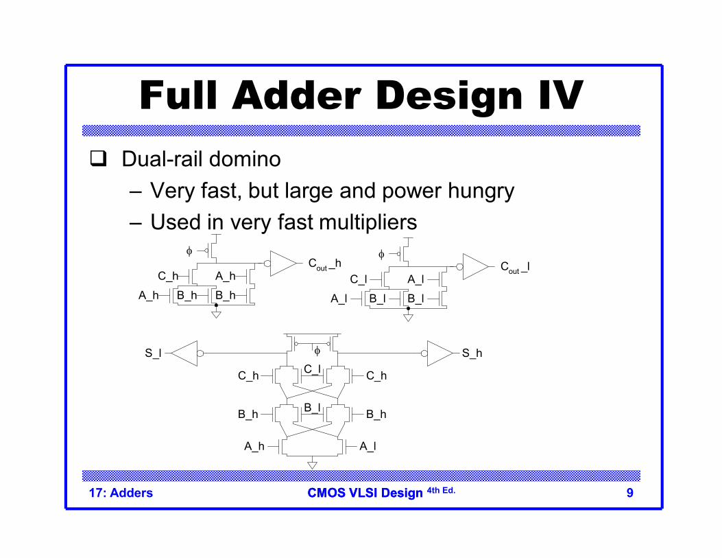
Full Adder Design IV Dual-rail domino
– Very fast, but large and power hungry– Used in very fast multipliers
Cout _h
A_h B_h
C_h
B_h
A_h
Cout _l
A_l B_l
C_l
B_l
A_l
S_hS_l
A_h
B_h B_hB_l
A_l
C_lC_h C_h

CMOS VLSI DesignCMOS VLSI Design 4th Ed.17: Adders 10
Carry Propagate Adders N-bit adder called CPA
– Each sum bit depends on all previous carries– How do we compute all these carries quickly?
+
BN...1AN...1
SN...1
CinCout 11111 1111 +0000 0000
A4...1
carries
B4...1
S4...1
CinCout
00000 1111 +0000 1111
CinCout

CMOS VLSI DesignCMOS VLSI Design 4th Ed.17: Adders 11
Carry-Ripple Adder Simplest design: cascade full adders
– Critical path goes from Cin to Cout
– Design full adder to have fast carry delay
CinCout
B1A1B2A2B3A3B4A4
S1S2S3S4
C1C2C3
CMOS VLSI DesignCMOS VLSI Design 4th Ed.
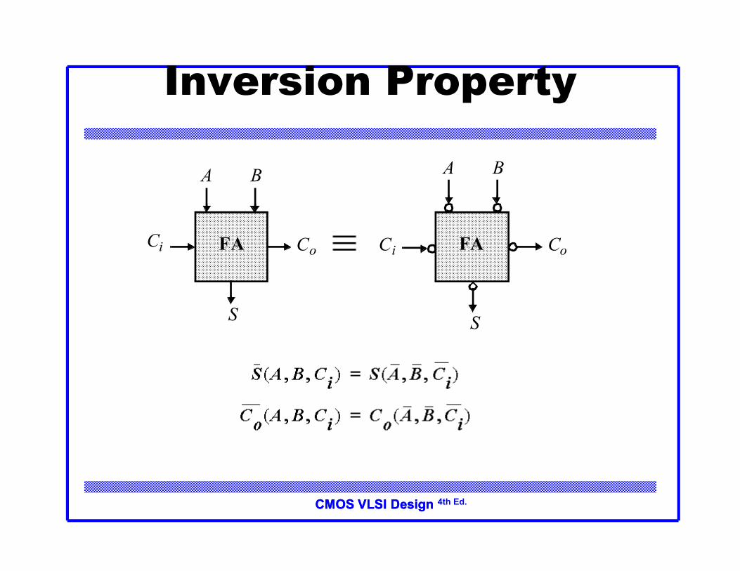
Inversion Property
A B
S
CoCi FA
A B
S
CoCi FA

CMOS VLSI DesignCMOS VLSI Design 4th Ed.
Minimize Critical Path by Reducing Inverting Stages
A0 B0
S0
Co,0Ci,0
A1 B1
S1
Co,1
A2 B2
S2
Co,2 Co,3FA’ FA’ FA’ FA’
A3 B3
S3
Odd CellEven Cell
Exploit Inversion Property
Note: need 2 different types of cells

CMOS VLSI DesignCMOS VLSI Design 4th Ed.17: Adders 14
Inversions Critical path passes through majority gate
– Built from minority + inverter– Eliminate inverter and use inverting full adder
Cout Cin
B1A1B2A2B3A3B4A4
S1S2S3S4
C1C2C3

CMOS VLSI DesignCMOS VLSI Design 4th Ed.17: Adders 15
Carry-Select Adder Trick for critical paths dependent on late input X
– Precompute two possible outputs for X = 0, 1– Select proper output when X arrives
Carry-select adder precomputes n-bit sums– For both possible carries into n-bit group
Cin+
A4:1 B4:1
S4:1
C4
+
+
01
A8:5 B8:5
S8:5
C8
+
+
01
A12:9 B12:9
S12:9
C12
+
+
01
A16:13 B16:13
S16:13
Cout
0
1
0
1
0
1

CMOS VLSI DesignCMOS VLSI Design 4th Ed.
Carry Select Adder
CMOS VLSI DesignCMOS VLSI Design 4th Ed.
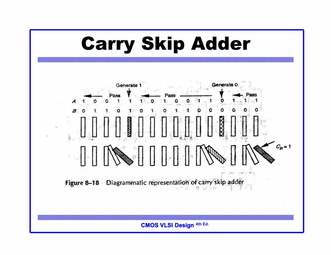
Carry Skip Adder
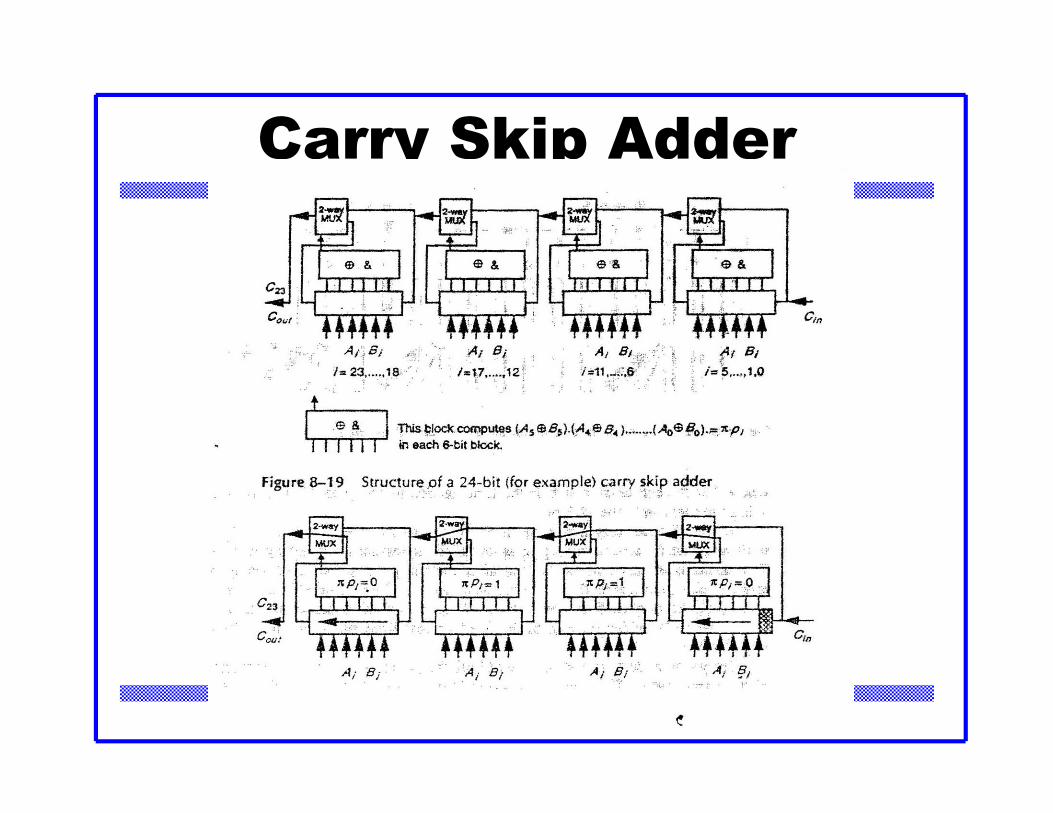
CMOS VLSI DesignCMOS VLSI Design 4th Ed.
Carry Skip Adder

CMOS VLSI DesignCMOS VLSI Design 4th Ed.
Carry Look Ahead Adder

CMOS VLSI DesignCMOS VLSI Design 4th Ed.
Carry Look Ahead Adder
in
in
CBABABABABACBABACCBABAC
))(()()()(
0011001111011111
00000

CMOS VLSI DesignCMOS VLSI Design 4th Ed.
Carry Look Ahead Adder

CMOS VLSI DesignCMOS VLSI Design 4th Ed.17: Adders 22
Carry-Lookahead Adder Carry-lookahead adder computes Gi:0 for many bits
in parallel. Uses higher-valency cells with more than two inputs.
Cin+
S4:1
G4:1P4:1
A4:1 B4:1
+
S8:5
G8:5P8:5
A8:5 B8:5
+
S12:9
G12:9P12:9
A12:9 B12:9
+
S16:13
G16:13P16:13
A16:13 B16:13
C4C8C12Cout

CMOS VLSI DesignCMOS VLSI Design 4th Ed.17: Adders 23
Tree Adder If lookahead is good, lookahead across lookahead!
– Recursive lookahead gives O(log N) delay Many variations on tree adders
CMOS VLSI DesignCMOS VLSI Design 4th Ed.17: Adders 24
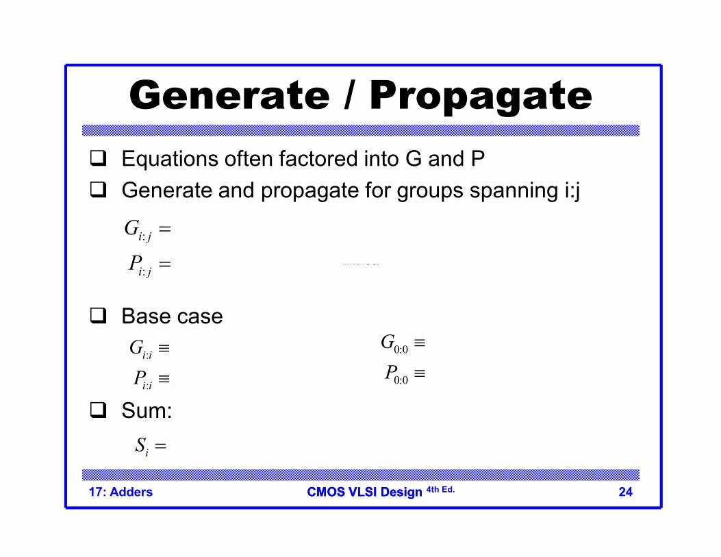
Generate / Propagate Equations often factored into G and P Generate and propagate for groups spanning i:j
Base case
Sum:
: : : 1:
: : 1:
i j i k i k k j
i j i k k j
G G P GP P P
�
�
:
:
i i i i i
i i i i i
G G A BP P A B
�
0:00:00inGCP0:00:00inGCP
0:0 0
0:0 0 0inG G C
P P
1:0i i iS P G
CMOS VLSI DesignCMOS VLSI Design 4th Ed.17: Adders 25
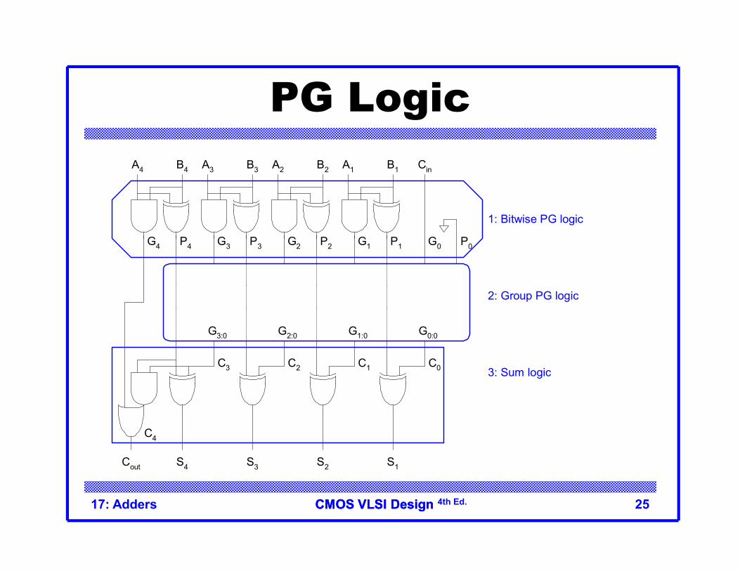
PG Logic
S1
B1A1
P1G1
G0:0
S2
B2
P2G2
G1:0
A2
S3
B3A3
P3G3
G2:0
S4
B4
P4G4
G3:0
A4 Cin
G0 P0
1: Bitwise PG logic
2: Group PG logic
3: Sum logicC0C1C2C3
Cout
C4

CMOS VLSI DesignCMOS VLSI Design 4th Ed.17: Adders 26
PG Carry-Ripple Addition:0 1:0 i i i iG G P G �
S1
B1A1
P1G1
G0:0
S2
B2
P2G2
G1:0
A2
S3
B3A3
P3G3
G2:0
S4
B4
P4G4
G3:0
A4 Cin
G0 P0
C0C1C2C3
Cout
C4 4-bit carry-ripple adder using PG logic

CMOS VLSI DesignCMOS VLSI Design 4th Ed.17: Adders 27
Carry-Ripple PG DiagramD
elay
0123456789101112131415
15:0 14:0 13:0 12:0 11:0 10:0 9:0 8:0 7:0 6:0 5:0 4:0 3:0 2:0 1:0 0:0
Bit Position
ripple xor( 1)pg AOt t N t t

CMOS VLSI DesignCMOS VLSI Design 4th Ed.17: Adders 28
PG Diagram Notation
i:j
i:j
i:k k-1:j
i:j
i:k k-1:j
i:j
Gi:k
Pk-1:j
Gk-1:j
Gi:j
Pi:j
Pi:k
Gi:k
Gk-1:j
Gi:j Gi:j
Pi:j
Gi:j
Pi:j
Pi:k
Black cell Gray cell Buffer

CMOS VLSI DesignCMOS VLSI Design 4th Ed.17: Adders 29
CLA PG Diagram
012345678910111213141516
15:0 14:0 13:0 12:0 11:0 10:0 9:0 8:0 7:0 6:0 5:0 4:0 3:0 2:0 1:0 0:016:0

CMOS VLSI DesignCMOS VLSI Design 4th Ed.17: Adders 30
Higher-Valency Cells
i:j
i:k k-1:l l-1:m m-1:j
Gi:k
Gk-1:l
Gl-1:m
Gm-1:j
Gi:j
Pi:j
Pi:k
Pk-1:l
Pl-1:m
Pm-1:j
CMOS VLSI DesignCMOS VLSI Design 4th Ed.
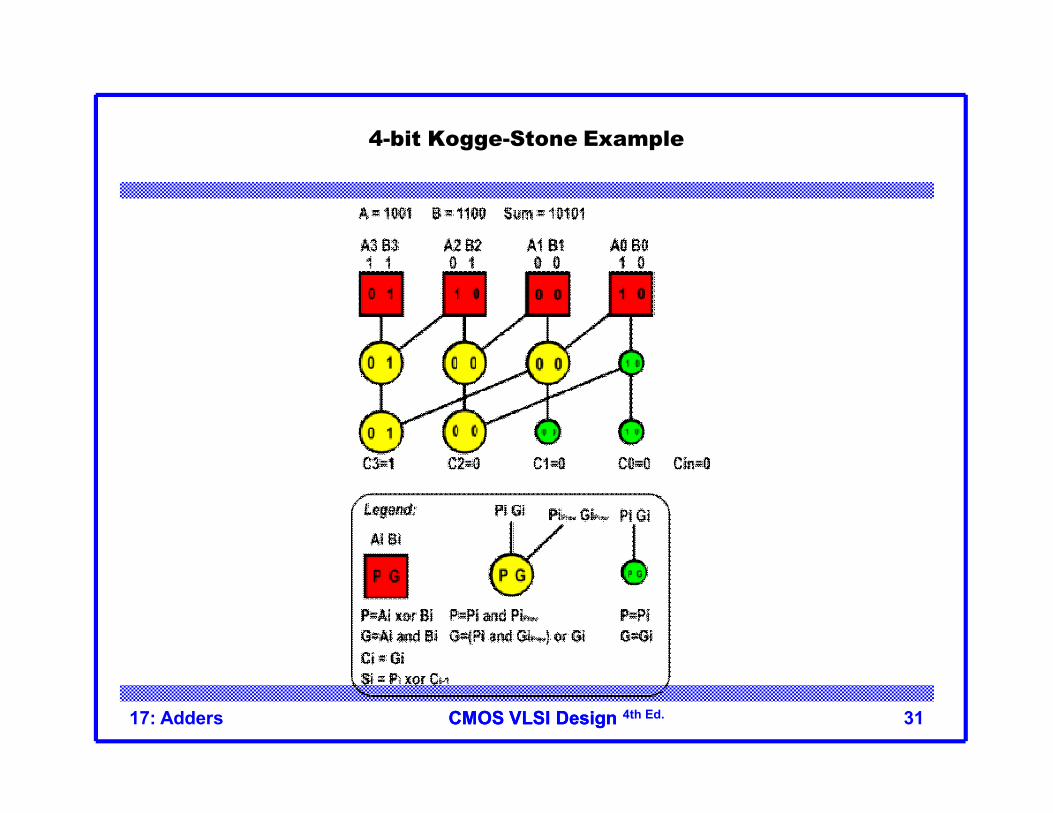
4-bit Kogge-Stone Example
17: Adders 31
CMOS VLSI DesignCMOS VLSI Design 4th Ed.17: Adders 32
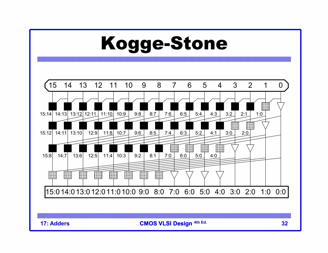
Kogge-Stone
1:02:13:24:35:46:57:68:79:810:911:1012:1113:1214:1315:14
3:04:15:26:37:48:59:610:711:812:913:1014:1115:12
4:05:06:07:08:19:210:311:412:513:614:715:8
2:0
0123456789101112131415
15:014:013:012:011:010:0 9:0 8:0 7:0 6:0 5:0 4:0 3:0 2:0 1:0 0:0

CMOS VLSI DesignCMOS VLSI Design 4th Ed.17: Adders 33
Tree Adder Taxonomy Ideal N-bit tree adder would have
– L = log N logic levels– Fanout never exceeding 2– No more than one wiring track between levels
Describe adder with 3-D taxonomy (l, f, t)– Logic levels: L + l– Fanout: 2f + 1– Wiring tracks: 2t
Known tree adders sit on plane defined byl + f + t = L-1
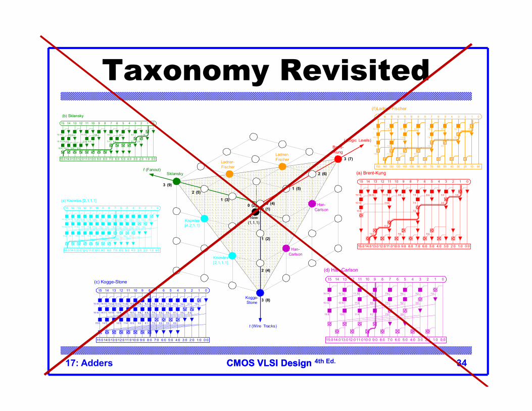
CMOS VLSI DesignCMOS VLSI Design 4th Ed.17: Adders 34
Taxonomy Revisited
f (Fanout)
t (Wire Tracks)
l (Logic Levels)
0 (2)1 (3)
2 (5)
3 (9)
0 (4)
1 (5)
2 (6)
3 (8)
2 (4)
1 (2)
0 (1)
3 (7)
Kogge-Stone
Sklansky
Brent-Kung
Han-Carlson
Knowles[2,1,1,1]
Knowles[4,2,1,1]
Ladner-Fischer
Han-Carlson
Ladner-Fischer
New(1,1,1)
(c) Kogge-Stone
1:02:13:24:35:46:57:68:79:810:911:1012:1113:1214:1315:14
3:04:15:26:37:48:59:610:711:812:913:1014:1115:12
4:05:06:07:08:19:210:311:412:513:614:715:8
2:0
0123456789101112131415
15:0 14:0 13:0 12:0 11:010:0 9:0 8:0 7:0 6:0 5:0 4:0 3:0 2:0 1:0 0:0
(e) Knowles [2,1,1,1]
1:02:13:24:35:46:57:68:79:810:911:1012:1113:1214:1315:14
3:04:15:26:37:48:59:610:711:812:913:1014:1115:12
4:05:06:07:08:19:210:311:412:513:614:715:8
2:0
0123456789101112131415
15:014:013:0 12:011:0 10:0 9:0 8:0 7:0 6:0 5:0 4:0 3:0 2:0 1:0 0:0
(b) Sklansky
1:0
2:03:0
3:25:47:69:811:1013:1215:14
6:47:410:811:814:1215:12
12:813:814:815:8
0123456789101112131415
15:0 14:013:0 12:011:010:0 9:0 8:0 7:0 6:0 5:0 4:0 3:0 2:0 1:0 0:0
1:03:25:47:69:811:1013:12
3:07:411:815:12
5:07:013:815:8
15:14
15:8 13:0 11:0 9:0
0123456789101112131415
15:0 14:0 13:0 12:0 11:0 10:0 9:0 8:0 7:0 6:0 5:0 4:0 3:0 2:0 1:0 0:0
(f) Ladner-Fischer
(a) Brent-Kung
1:03:25:47:69:811:1013:1215:14
3:07:411:815:12
7:015:8
11:0
5:09:013:0
0123456789101112131415
15:014:013:0 12:011:010:0 9:0 8:0 7:0 6:0 5:0 4:0 3:0 2:0 1:0 0:0
1:03:25:47:69:811:1013:1215:14
3:05:27:49:611:813:1015:12
5:07:09:211:413:615:8
0123456789101112131415
15:014:013:0 12:0 11:010:0 9:0 8:0 7:0 6:0 5:0 4:0 3:0 2:0 1:0 0:0
(d) Han-Carlson
CMOS VLSI DesignCMOS VLSI Design 4th Ed.17: Adders 35
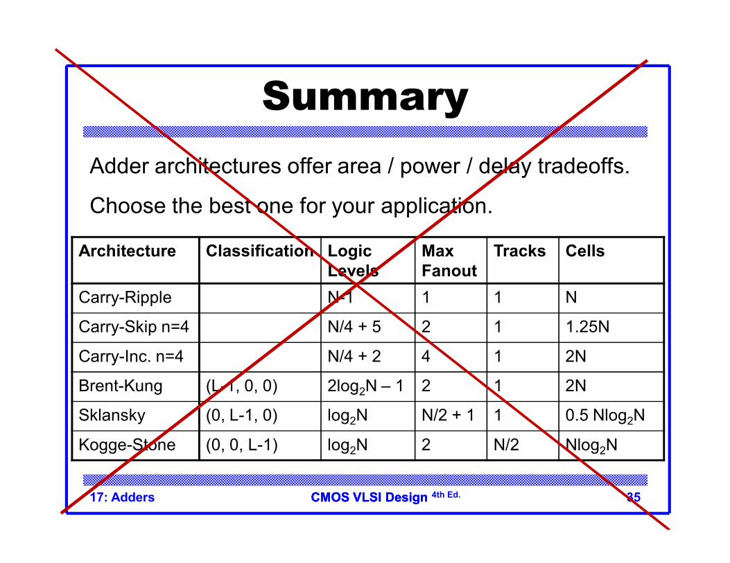
Summary
Architecture Classification Logic Levels
Max Fanout
Tracks Cells
Carry-Ripple N-1 1 1 N
Carry-Skip n=4 N/4 + 5 2 1 1.25N
Carry-Inc. n=4 N/4 + 2 4 1 2N
Brent-Kung (L-1, 0, 0) 2log2N – 1 2 1 2N
Sklansky (0, L-1, 0) log2N N/2 + 1 1 0.5 Nlog2N
Kogge-Stone (0, 0, L-1) log2N 2 N/2 Nlog2N
Adder architectures offer area / power / delay tradeoffs.
Choose the best one for your application.

CMOS VLSI DesignCMOS VLSI Design 4th Ed.18: Datapath Functional Units 36
Multiplication Example:
M x N-bit multiplication– Produce N M-bit partial products– Sum these to produce M+N-bit product
1100 : 1210 0101 : 510 1100 0000 1100 000000111100 : 6010
multipliermultiplicand
partialproducts
product

CMOS VLSI DesignCMOS VLSI Design 4th Ed.18: Datapath Functional Units 37
General Form Multiplicand: Y = (yM-1, yM-2, …, y1, y0) Multiplier: X = (xN-1, xN-2, …, x1, x0)
Product:1 1 1 1
0 0 0 02 2 2
M N N Mj i i j
j i i jj i i j
P y x x y
x0y5 x0y4 x0y3 x0y2 x0y1 x0y0
y5 y4 y3 y2 y1 y0
x5 x4 x3 x2 x1 x0
x1y5 x1y4 x1y3 x1y2 x1y1 x1y0
x2y5 x2y4 x2y3 x2y2 x2y1 x2y0
x3y5 x3y4 x3y3 x3y2 x3y1 x3y0
x4y5 x4y4 x4y3 x4y2 x4y1 x4y0
x5y5 x5y4 x5y3 x5y2 x5y1 x5y0
p0p1p2p3p4p5p6p7p8p9p10p11
multipliermultiplicand
partialproducts
product

CMOS VLSI DesignCMOS VLSI Design 4th Ed.
The Binary Multiplication
1 0 1 1
1 0 1 0 1 0
0 0 0 0 0 0
1 0 1 0 1 0
1 0 1 0 1 0
1 0 1 0 1 0
1 1 1 0 0 1 1 1 0
+
Partial Products
AND operation
CMOS VLSI DesignCMOS VLSI Design 4th Ed.18: Datapath Functional Units 39
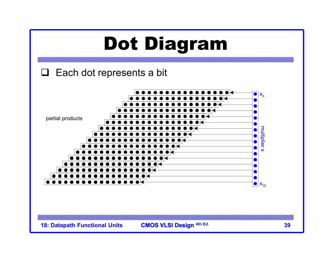
Dot Diagram Each dot represents a bit
partial products
multiplier x
x0
x15

CMOS VLSI DesignCMOS VLSI Design 4th Ed.18: Datapath Functional Units 40
Array Multipliery0y1y2y3
x0
x1
x2
x3
p0p1p2p3p4p5p6p7
B
ASin Cin
SoutCout
BA
CinCout
Sout
Sin
=
CSAArray
CPA
critical path BA
Sout
Cout CinCout
Sout
=Cin
BA
CMOS VLSI DesignCMOS VLSI Design 4th Ed.
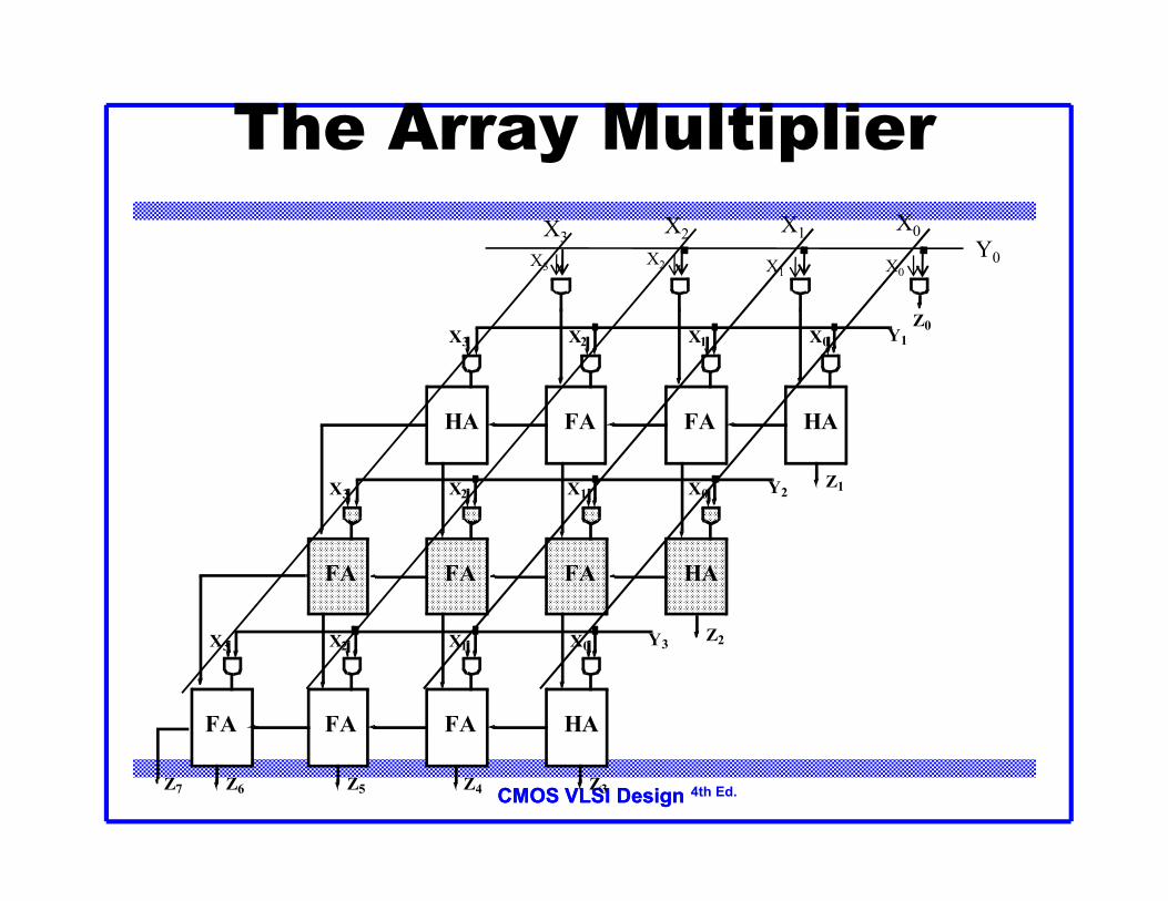
The Array Multiplier
HA FA FA HA
FA FA FA HA
FA FA FA HA
X0X1X2X3 Y1
X0X1X2X3 Y2
X0X1X2X3 Y3
Z1
Z2
Z3Z4Z5Z6
Z0
Z7
X0X1X2X3
Y0
X0X1X2X3

CMOS VLSI DesignCMOS VLSI Design 4th Ed.
The MxN Array Multiplier— Critical Path
HA FA FA HA
HAFAFAFA
FAFA FA HA
Critical Path 1
Critical Path 2
Critical Path 1 & 2

CMOS VLSI DesignCMOS VLSI Design 4th Ed.18: Datapath Functional Units 43
Rectangular Array Squash array to fit rectangular floorplan
y0y1y2y3
x0
x1
x2
x3
p0
p1
p2
p3
p4p5p6p7

CMOS VLSI DesignCMOS VLSI Design 4th Ed.
Carry-Save Multiplier
HA HA HA HA
FAFAFAHA
FAHA FA FA
FAHA FA HA
Vector Merging Adder
CMOS VLSI DesignCMOS VLSI Design 4th Ed.
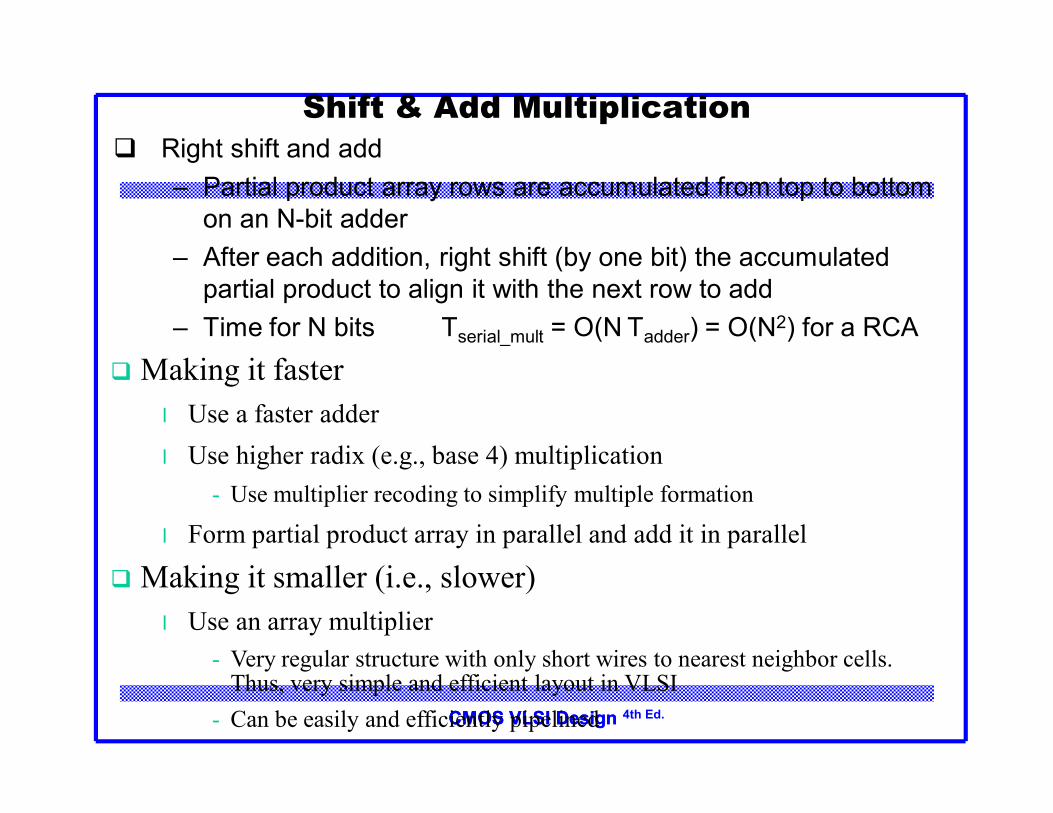
Shift & Add Multiplication Right shift and add
– Partial product array rows are accumulated from top to bottom on an N-bit adder
– After each addition, right shift (by one bit) the accumulated partial product to align it with the next row to add
– Time for N bits Tserial_mult = O(N Tadder) = O(N2) for a RCA Making it faster
l Use a faster adderl Use higher radix (e.g., base 4) multiplication
- Use multiplier recoding to simplify multiple formation
l Form partial product array in parallel and add it in parallel
Making it smaller (i.e., slower)l Use an array multiplier
- Very regular structure with only short wires to nearest neighbor cells. Thus, very simple and efficient layout in VLSI
- Can be easily and efficiently pipelined

CMOS VLSI DesignCMOS VLSI Design 4th Ed.
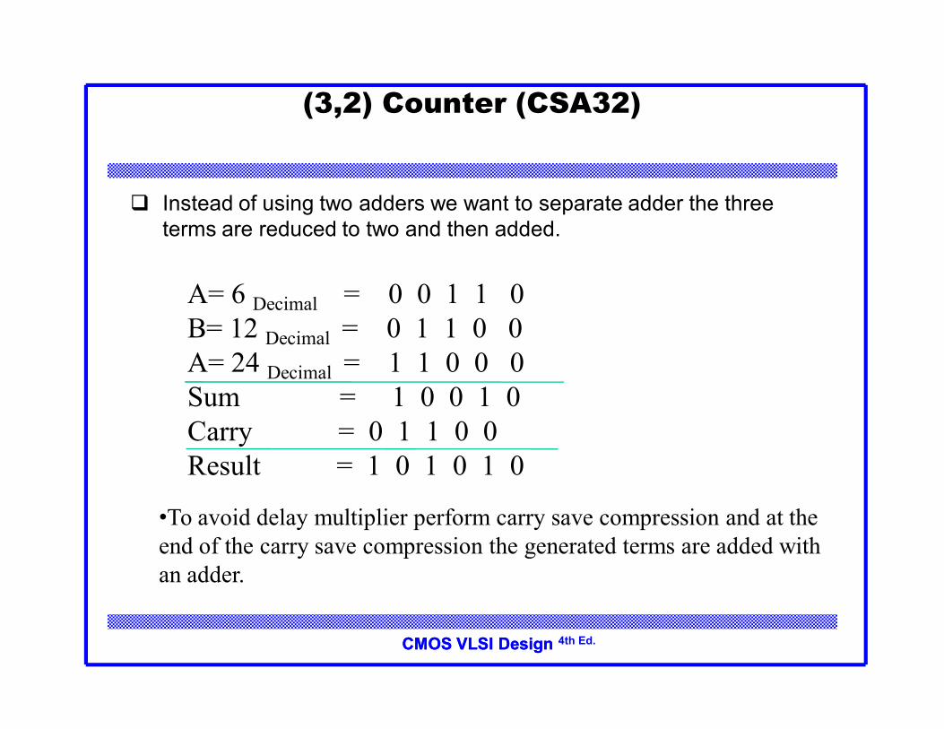
(3,2) Counter (CSA32)
A CSA is effectively a “1”s counter that adds the number of 1’S on the A,B, and C inputs and encode them on the sum and carry output.
A B C Carry Sum No of 1’s
0 0 0 0 0 00 0 1 0 1 10 1 0 0 1 10 1 1 1 0 21 0 0 0 1 11 0 1 1 0 21 1 0 1 0 21 1 1 1 1 3
CMOS VLSI DesignCMOS VLSI Design 4th Ed.
(3,2) Counter (CSA32)
Instead of using two adders we want to separate adder the three terms are reduced to two and then added.
A= 6 Decimal = 0 0 1 1 0B= 12 Decimal = 0 1 1 0 0A= 24 Decimal = 1 1 0 0 0Sum = 1 0 0 1 0Carry = 0 1 1 0 0Result = 1 0 1 0 1 0
•To avoid delay multiplier perform carry save compression and at the end of the carry save compression the generated terms are added with an adder.
CMOS VLSI DesignCMOS VLSI Design 4th Ed.
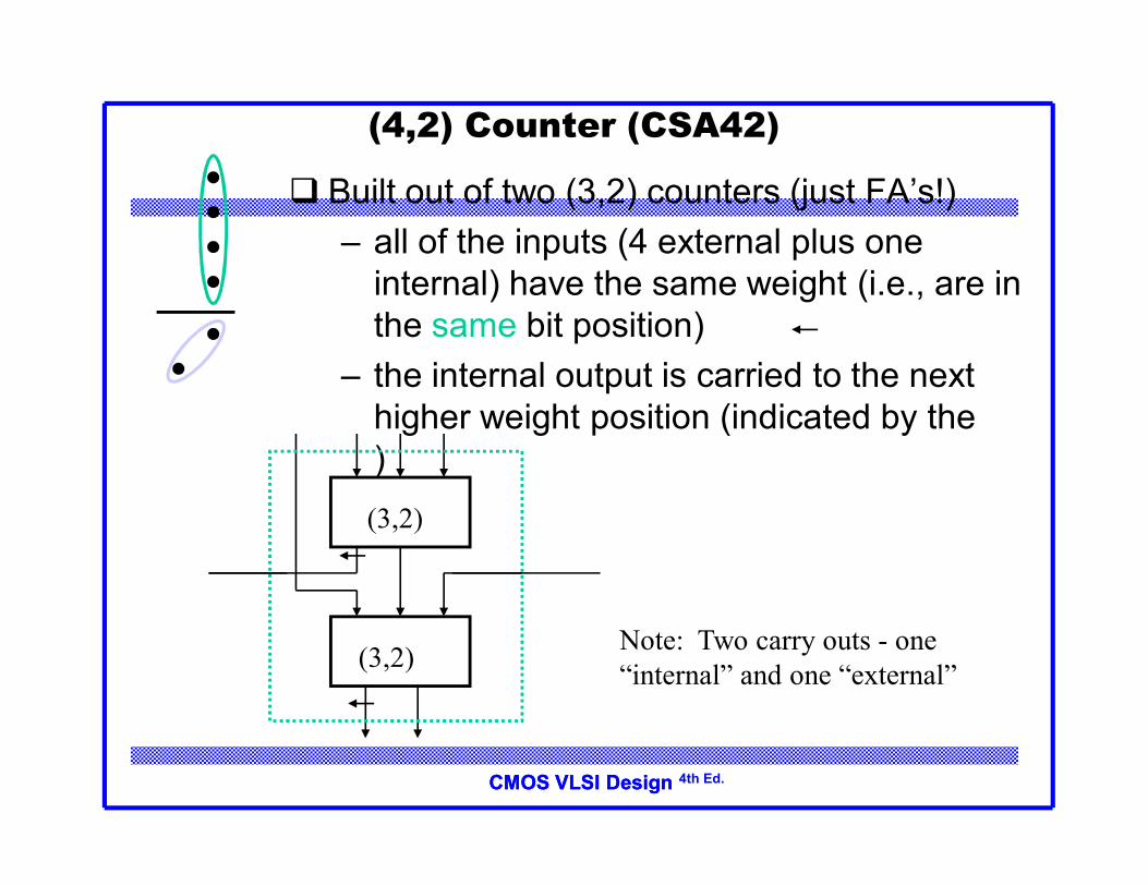
(4,2) Counter (CSA42)
Built out of two (3,2) counters (just FA’s!)– all of the inputs (4 external plus one
internal) have the same weight (i.e., are in the same bit position)
– the internal output is carried to the next higher weight position (indicated by the )(3,2)
(3,2) Note: Two carry outs - one “internal” and one “external”
CMOS VLSI DesignCMOS VLSI Design 4th Ed.
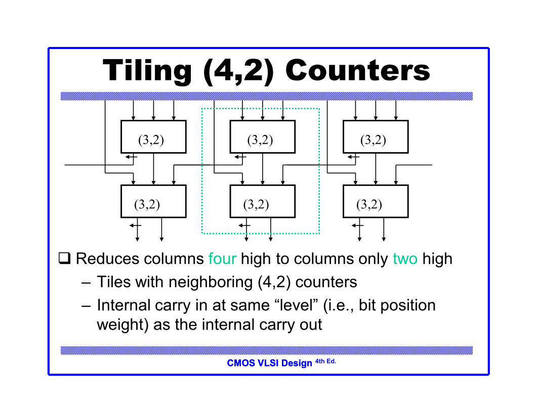
Tiling (4,2) Counters
Reduces columns four high to columns only two high– Tiles with neighboring (4,2) counters– Internal carry in at same “level” (i.e., bit position
weight) as the internal carry out
(3,2)
(3,2)
(3,2)
(3,2)
(3,2)
(3,2)

CMOS VLSI DesignCMOS VLSI Design 4th Ed.
Tiling (4,2) Counters
Reduces columns four high to columns only two high– Tiles with neighboring (4,2) counters– Internal carry in at same “level” (i.e., bit position
weight) as the internal carry out
(3,2)
(3,2)
(3,2)
(3,2)
(3,2)
(3,2)

CMOS VLSI DesignCMOS VLSI Design 4th Ed.
4x4 Partial Product Array Reduction
multiplicandmultiplier
partialproductarray
reduced pp array (to CPA)
double precision product
Fast 4x4 multiplication using (4,2) counters

CMOS VLSI DesignCMOS VLSI Design 4th Ed.
4x4 Partial Product Array Reduction
multiplicandmultiplier
partialproductarray
reduced pp array (to CPA)
double precision product
Fast 4x4 multiplication using (4,2) counters

CMOS VLSI DesignCMOS VLSI Design 4th Ed.
8x8 Partial Product Array Reduction‘icand‘ier
partialproductarray
How many (4,2) counters minimum are needed to reduce it to 2 rows?

CMOS VLSI DesignCMOS VLSI Design 4th Ed.
8x8 Partial Product Array Reduction‘icand‘ier
partialproductarray
reduced partial product array
How many (4,2) countersminimum are needed to reduce it to 2 rows?
Answer: 24

CMOS VLSI DesignCMOS VLSI Design 4th Ed.
Alternate 8x8 Partial Product Array Reduction‘icand‘ier
partialproductarray
reduced partial product array
More (4,2) counters, so what is the advantage?

CMOS VLSI DesignCMOS VLSI Design 4th Ed.
Wallace Tree Multiplication
18: Datapath Functional Units 56

CMOS VLSI DesignCMOS VLSI Design 4th Ed.
Wallace Tree Multiplication
17: Adders 57

CMOS VLSI DesignCMOS VLSI Design 4th Ed.18: Datapath Functional Units 58
Fewer Partial Products Array multiplier requires N partial products If we looked at groups of r bits, we could form N/r
partial products.– Faster and smaller?– Called radix-2r encoding
Ex: r = 2: look at pairs of bits– Form partial products of 0, Y, 2Y, 3Y– First three are easy, but 3Y requires adder

CMOS VLSI DesignCMOS VLSI Design 4th Ed.18: Datapath Functional Units 59
Booth Encoding Instead of 3Y, try –Y, then increment next partial
product to add 4Y Similarly, for 2Y, try –2Y + 4Y in next partial product

CMOS VLSI DesignCMOS VLSI Design 4th Ed.18: Datapath Functional Units 60
Booth Hardware Booth encoder generates control lines for each PP
– Booth selectors choose PP bits


![Chapter 11 · 2. COMPARISON OF VLSI ADDERS The most common approach in comparing VLSI adders was to use of a single delay point [1,2]. An example of such comparison (based only on](https://img.dokumen.tips/doc/110x75/5f44fd1856be9f2faa76e1d7/chapter-11-2-comparison-of-vlsi-adders-the-most-common-approach-in-comparing-vlsi.jpg)