Embed Size (px)
Citation preview

High-Speed VLSI Arithmetic Units: Adders and Multipliers
by
Prof. Vojin G. Oklobdzija
Fall 1999

Oklobdzija: HIGH-SPEED VLSI ARITHMETIC UNITS: ADDERS AND MULTIPLIERS
5:12 PM September 13, 19992
Introduction
Digital computer arithmetic is an aspect of logic design with the objective of developingappropriate algorithms in order to achieve an efficient utilization of the available hardware [1-4].Given that the hardware can only perform a relatively simple and primitive set of Booleanoperations, arithmetic operations are based on a hierarchy of operations that are built upon thesimple ones. Since ultimately, speed, power and chip area are the most often used measures ofthe efficiency of an algorithm, there is a strong link between the algorithms and technology usedfor its implementation.
High-speed Addition: Algorithms and VLSI Implementation:
First we will examine a realization of a one-bit adder which represents a basic building block forall the more elaborate addition schemes.
Full Adder:Operation of a Full Adder is defined by the Boolean equations for the sum and carry signals:
iiiiiiiiiiiiiiii cbacbacbacbacbas ⊕⊕=+++=
iiiiiiiiiiiii cbacbacbacbac +++=+1
Where: ai, bi, and ci are the inputs to the i-th full adder stage, and si and ci+1 are the sum andcarry outputs from the i-th stage, respectively.From the above equation we realize that the realization of the Sum function requires two XORlogic gates.The Carry function is further rewritten defining the Carry-Propagate pi and Carry-Generate gi
terms:
iii bap ⊕= , iii bag •=At a given stage i, a carry is generated if gi is true (i.e., both ai and bi are ONEs), and if pi is true,a stage propagates an input carry to its output (i.e., either ai or bi is a ONE). The logicalimplementation of the full adder is shown in Fig. 1.a.
Fig. 1.a.b. Full-Adder implementation (a) regular (b) using multiplexer in the critical path
cout cin
si
ai bi
0
1s
biai
cout
si
cin
(a.) (b.)

Oklobdzija: HIGH-SPEED VLSI ARITHMETIC UNITS: ADDERS AND MULTIPLIERS
5:12 PM September 13, 19993
For this implementation, the delay from either a or bi to si is two XOR delays and the delay fromci to ci+1 is 2 gate delays. Some technologies, such as CMOS, implement the functions moreefficiently by using pass-transistor circuits. For example, the critical path of the carry-in to carry-out uses a fast pass-transistor multiplexer [8] in an alternative implementation of the Full Addershown in Fig.1.b.
The ability of pass-transistor logic to provide an efficient multiplexer implementation has beenexploited in CPL and DPL logic families [10,11]. Even an XOR gate is more efficientlyimplemented using multiplexer topology. A Full-Adder cell which is entirely multiplexer basedas published by Hitachi [11] is shown in Fig.2. Such a Full-Adder realization contains only twotransistors in the Input-to-Sum path and only one transistor in the Cin-to-Cout path (not countingthe buffer). The short critical path is a factor that contributes to a remarkable speed of thisimplementation.
Fig.2. Pass-Transistor realization of a Full-Adder in DPL [11]
A
A
B
B
C C
VCCS
S
XOR/XNOR MULTIPLEXER BUFFER
C C
MULTIPLEXER
VCCC
O
CO
BUFFER
VCC
VCC
OR/NOR
AND/NAND
A
A
B
B
A
A
B
B

Oklobdzija: HIGH-SPEED VLSI ARITHMETIC UNITS: ADDERS AND MULTIPLIERS
5:12 PM September 13, 19994
Ripple Carry Adder:A ripple carry adder for N-bit numbers is implemented by concatenating N full adders as shownon Figure 3. At the i-th bit position, the i-th bits of operands A and B and a carry signal from thepreceding adder stage are used to generate the i-th bit of the sum, si, and a carry, ci+1, to the nextadder stage. This is called a Ripple Carry Adder (RCA), since the carry signal “ripple” from theleast significant bit position to the most significant [3-4]. If the ripple carry adder isimplemented by concatenating N full adders, the delay of such an adder is 2N gate delays fromCin-to-Cout.
The path from the input to the output signal that is likely to take the longest time is designated asa "critical path". In the case of a RCA, this is the path from the least significant input a0 or b0 tothe last sum bit sn. Assuming a multiplexer based XOR gate implementation, this critical pathwill consist of N+1 pass transistor delays. However, such a long chain of transistors willsignificantly degrade the signal, thus some amplification points are necessary. In practice, we canuse a multiplexer cell to build this critical path using standard cell library as shown in Fig.3 [8].
Fig. 3. Carry-Chain of an RCA implemented using multiplexer from the standard cell library [8]
Carry Skip Adder:Since the Cin-to-Cout represents the longest path in the ripple-carry-adder an obvious attempt is toaccelerate carry propagation through the adder. This is accomplished by using Carry-Propagatepi signals within a group of bits. If all the pi signals within the group are pi = 1, the conditionexist for the carry to bypass the entire group:
kiiii ppppP +++ ••••= ......21
The Carry Skip Adder (CSKA) divides the words to be added into groups of equal size of k-bits.The basic structure of an N-bit Carry Skip Adder is shown on Fig. 4. Within the group, carrypropagates in a ripple-carry fashion. In addition, an AND gate is used to form the group
ai+1 bi+1 ai biai+2 bi+2
cout
ci+1 ci
sisi+1si+2
cin

Oklobdzija: HIGH-SPEED VLSI ARITHMETIC UNITS: ADDERS AND MULTIPLIERS
5:12 PM September 13, 19995
propagate signal P. If P = 1 the condition exists for carry to bypass (skip) over the group asshown in Fig.4.
Fig.4. Basic Structure of a CSA: N-bits, k-bits/group, r=N/k groups
The maximal delay of a Carry Skip Adder is encountered when carry signal is generated in theleast-significant bit position, rippling through k-1 bit positions, skipping over N/k-2 groups in themiddle, rippling to the k-1 bits of most significant group and being assimilated in the Nth bitposition to produce the sum SN:
SKIPrcarcaSKIPrcaCSA
Nkk
Nk ∆−+∆−=∆−+∆−+∆−=∆ )2
2()1(2)1()2
2()1(
Thus, CSKA is faster than RCA at the expense of a few relatively simple modifications. Thedelay is still linearly dependent on the size of the adder N, however this linear dependence isreduced by a factor of 1/k [3].
Fig.5. Carry-chain of a 32-bit Variable Block Adder
Gr G r-1
...
SN-k-1SN-1
aN-1 bN-1 b N-k-1aN-k-1
S(r-1)k-1 S (r-2)k
G1Go
...
Sk
S2k-1
a 2k-1b 2k-1 bk
ak
Sk-1
S0
...
...a (r-1)k b(r-1)k a (r-1)k b (r-1)k
...a k-1 b k-1 a0 b0
...
Cin
... ... ... ... ... ... ... ...
Pr-1 Pr-2 P1 P0
Cout + + + +
AND
OROROR OR
ANDANDAND
critical path, delay ∆=2(k-1)+(N/2-2)
G0
... ...
a0 b
0
...
...
ai
bi
aN-1
bN-1
Sj
Pm-2
CinCout
Cou
t
G2Gm-2Gm-1Gm
G0G1G2Gm-2Gm-1Gm
SN-1 SiS0
P2P0Pm-1Pm
.....
G1
P1
Cin
.....
aj b
j
Carry signal path
skiping
rippling

Oklobdzija: HIGH-SPEED VLSI ARITHMETIC UNITS: ADDERS AND MULTIPLIERS
5:12 PM September 13, 19996
Variable Block Adder:The idea behind Variable Block Adder (VBA) is to minimize the longest critical path in the carrychain of a CSKA, while allowing the groups to take different sizes [2,7]. Such an optimization ingeneral does not result in an enhanced complexity as compared to the CSKA. A carry-chain of a32-bit VBA is shown in Fig.5.The first and last blocks are smaller, and the intermediate blocks are larger. That compensates forthe critical paths originating from the ends by shortening the length of the path used for the carrysignal to ripple in the end groups, allowing carry to skip over larger groups in the middle.There are two important consequences of this optimization:
(a.) First, the total delay is reduced as compared to CSKA(b.) Second, the delay dependency is not a linear function of the adder size N as in CSKA.
This dependency follows a square root function of N instead.
For an optimized VBA, it is possible to obtain a close form solution expressing this delay
dependency which is given as: 321 cNccVBA ++=∆ where: c1, c2, c3 are constants.
It is also possible to extend this approach to multiple levels of carry skip as done in [7]. Adetermination of the optimal sizes of the blocks on the first and higher levels of skip blocks is alinear programming problem which does not yield a close form solution. Such types of problemsare solved with the use of dynamic programming techniques. The speed of such a multiple-levelVBA adder surpasses single-level VBA and that of fixed group Carry-Lookahead Adder (CLA).[15]. There are two reasons why this is possible:
(1.) First, the speed of the logic gates used for CMOS implementation depends on the outputload: fan-out, as well as the number of inputs: fan-in. CLA implementation is characterizedwith a large fan-in which limits the available size of the groups. On the other hand VBAimplementation is simple. Thus, it seems that CLA has passed the point of diminishingreturns as far as an efficient implementation is concerned. This example also points to theimportance of modeling and incorporating appropriate technology parameters into thealgorithm. Most of the computer arithmetic algorithms developed in the past use a simpleconstant gate delay model.
(2.) Second, a fixed-group CLA is not the best way to build an adder. It is a sub-optimal structurewhich after being optimized for speed, consists of groups that are different in size yielding alargely irregular structure [15].
There are other advantages of VBA adder that are direct result of its simplicity and efficientoptimization of the critical path. Those advantages are exhibited in the lower area and powerconsumption while retaining its speed. Thus, VBA has the lowest energy-delay product ascompared to the other adders in its class. [9].Carry Lookahead Adder: A significant speed improvement in the implementation of a parallel adder was introduced by aCarry-Lookahead-Adder (CLA) developed by Weinberger and Smith in 1958 [13]. The CLAadder is theoretically one of the fastest schemes used for the addition of two numbers, since thedelay to add two numbers depends on the logarithm of the size of the operands: Nlog≈∆

Oklobdzija: HIGH-SPEED VLSI ARITHMETIC UNITS: ADDERS AND MULTIPLIERS
5:12 PM September 13, 19997
The Carry Loookahead Adder uses modified full adders (modified in the sense that a carryoutput is not formed) for each bit position and Lookahead modules which are used to generatecarry signals independently for a group of k-bits. In most common case k=4. In addition to carrysignal for the group, Lookahead modules produce group carry generate (G) and group carrypropagate (P) outputs that indicate that a carry is generated within the group, or that an incomingcarry would propagate across the group.Extending the carry equation to a second stage in a Ripple-Carry-Adder we obtain:
1111
111
1112
)(
cppgpg
cpgpg
cpgc
iiiii
iiii
iiii
+++
++
++++
++=
++=
+=
This carry equation results from evaluating the carry equation for the i+1-st stage andsubstituting ci+1. Carry ci+2 exits from stage i+1 if:
(a.) a carry is generated in the stage i+1 or
(b.) a carry is generated in stage i and propagates across stage i+1 or
(c.) a carry enters stage i and propagates across both stages i and i+1, etc.
Extending the carry equation to a third stage yields:
ii1i2ii1i2i1i2i2i
ii1i1i1i2i2i
2i2i2i3i
cppp gpp gp g
)cpp gp (gp g
cp g c
+++++++
+++++
++++
+++=
+++=
+=
i
Although it would be possible to continue this process indefinitely, each additional stageincreases the size (i.e., the number of inputs) of the logic gates. Four inputs (as required toimplement ci+3 equation ) is frequently the maximum number of inputs per gate for currenttechnologies. To continue the process, Carry-Lookahead utilizes group generate and grouppropagate signals over four bit groups (stages i to i+3), Gi and Pi, respectively:
i1i2i3i1i2i3i2i3i3i gppp gpp gp g +++++++++ +++=iG
and:
i1i2i3ii pppp P +++=
The carry equation can be expressed in terms of the four bit group generate and propagatesignals:

Oklobdzija: HIGH-SPEED VLSI ARITHMETIC UNITS: ADDERS AND MULTIPLIERS
5:12 PM September 13, 19998
iii cPG +=+1ic
Thus, the carry out from a 4-bit wide group ci+4 can be computed in four gate delays: one gatedelay to compute pi and gi for i = i through i+3, a second gate delay to evaluate Pi, the secondand the third to evaluate Gi, and the third and fourth to calculate carry signals ci+1, ci+2 , ci+3 andci+4. Actually, if not limited by fan-in constraints, ci+4 could be calculated concurrently with Gi
and will be available after three gate delays.In general, an k bit lookahead group requires 0.5(3k+k2) logic gates, where k is the size of thegroup. In a recursive fashion, we can create a "group of groups" or a "super-group". The inputsto the "super-group" are G and P signals from the previous level. The "super-group" produces P*
and G* signals indicating that the carry signal will be propagated across all of the groups withinthe "super-group" domain, or that the carry will be generated in one of the groups encompassedby the "super-group". Similarly to the group, a "super-group" produces a carry signal out of the"super-group" as well as an input carry signal for each of the groups in the level above:
iiiiiiiiiij GPPPGPPGPG 123123233*G +++++++++ +++=
iiiij PPPPP 123*
+++=
ijjj cPG +=c
A construction of a 32-bit Carry Lookahead Adder is illustrated in Fig. 6.
Fig. 6. 32-bit Carry Lookahead Adder
Cin
Cout Cin
C4C8C12
Cout
C20C24C28
Cin
C16
aibi
individual addersgenerating: g i, p i,
and sum S i
Carry-lookahead blocks of4-bits generating:
Gi, P i, and C in for theadders
Carry-lookahead super- blocks of4-bits blocks generating:
G* i, P* i, and C in for the 4-bitblocks
Group producing finalcarry Cout and C 16
Critical path delay = 1∆ (for gi,pi)+2x2 ∆ (for G,P)+3x2 ∆ (for Cin)+1XOR- ∆ (for Sum) = appx. 12 ∆ of delay

Oklobdzija: HIGH-SPEED VLSI ARITHMETIC UNITS: ADDERS AND MULTIPLIERS
5:12 PM September 13, 19999
As opposed to RCA or CSA the critical path in the CLA travels in vertical direction rather than ahorizontal one as shown in Fig.6. Therefore the delay of CLA is not directly proportional to thesize of the adder N, but to the number of levels used. Given that the groups and super-groups inthe CLA resemble a tree structure the delay of a CLA is thus proportional to the log function ofthe size N.CLA delay is evaluated by recognizing that an adder with a single level of carry lookahead (fourbit words) contains three gate delays in the carry path. Each additional level of lookaheadincreases the maximum word size by a factor of k and adds two additional gate delays.Generally the number of lookahead levels for an N-bit adder is logk N where k+1 is themaximum number of inputs per gate. Since an k-bit group carry-lookahead adder introducesthree gate delays per CLA level, and there are two additional gate delays: one for gi and pi, andother for the final sum si, CLA delay ∆ is:
NNCLA log41)1log =+−2( + 1 = ∆
This log dependency makes CLA one of the theoretically fastest structures for addition [2-4].However, it can be argued that the speed efficiency of the CLA has passed the point ofdiminishing returns given the fan-in and fan-out dependencies of the logic gates and inadequacyof the delay model based on counting number of gates in the critical path. In reality, CLA isindeed achieving lesser speed than expected, especially when compared to some techniques thatconsume less hardware for the implementation as shown in [7,8].One of the simple schemes for addition that was very popular at the time when transition intoMOS technology was made, is Manchester Carry Chain (MCC) [6,38]. MCC is an alternativeswitch based technique implemented using pass-transistor logic. The speed realized using MCCis impressive which is due to its simplicity and the properties of the pass-transistor logic. MCCdoes not require a large area for its implementation, consuming substantially less power ascompared to CLA or other more elaborate schemes. A realization of the MCC is shown in Fig. 7.Due to the RC delay properties of the MCC the signal needs to be regenerated by insertinginverters at appropriately chosen locations in the carry chain.
Fig. 7. Manchester Carry-Chain realization of the carry path.
Vdd
Carry out Carry in
Propagatedevice
Predischarge& kill device
Generatedevice
++++++++
VddVddVddVddVddVddVdd

Oklobdzija: HIGH-SPEED VLSI ARITHMETIC UNITS: ADDERS AND MULTIPLIERS
5:12 PM September 13, 199910
In the same way a CLA can be built using MCC for the implementation of the lookahead group.Further, pass-transistor MCC structure can be incorporated in the logic group of the circuittechnology used for CLA realization. One such an example is shown in Fig. 8.a. representing afour bit group of an 64-bit CLA built using CMOS Domino logic [14]. Each CLA group isimplemented as a separate CMOS Domino function. This adder built by Motorola using 1.0uCMOS technology achieved a remarkable speed of 4.5nS at VDD=5V and 25oC. The critical pathof this design is shown in Fig. 8.b. Using selection technique and careful analysis of the criticalpath the same adder was extended to 96-bits at the same speed of 4.5nS.As with RCA, the carry lookahead adder complexity grows linearly with the word size (for k = 4,this occurs at a 40% faster rate than the RCA).
Fig. 8.a. CMOS Domino realization of a 64-bit CLA
P3:0
P2:0
P1:0
C3
C2
C1
C0
G0P0
G1P1
G2P2
G3P3
G3:0
G2:0
G1:0

Oklobdzija: HIGH-SPEED VLSI ARITHMETIC UNITS: ADDERS AND MULTIPLIERS
5:12 PM September 13, 199911
Fig. 8.b. Critical path in Motorola's 64-bit CLA [14]
Recurrence Solver Based Adders:The class of adders known as based on solving recurrence equations was first introduced byBiolgory and Gajski and Brent and Kung [17],[18] based on the previous work by Koggie andStone [16].
Fig. 9. Recurrence Solver adder topology
Critical path: A, B - G0 - G3:0 - G15:0 - G47:0 - C48 - C60 - C63 - S63
G4
P7
G0
P0
G1
P1
G2
P2
G3
P3
...
CARRYBLOCK
G8
P11
... G12
P15
... G16
P31
... G32
P47
... G48
P51
G60
P60
G61
P61
G62
P62
G63
P63
... G52
P55
... G56
P59
...
PG BLOCK
PG BLOCK
PG BLOCK
PG BLOCK
P,G
0
P,G
1:0
P,G
2:0
G3:0
P3:0
G7:4
P7:4
G11:8
P11:8
G15:12
P15:12
G3:0
P3:0
G7:0
P7:0
G11:0
P11:0
G15:0
P15:0
G15:0
P15:0
G31:16
P31:16
G31:0
P31:0
G47:32
P47:32
G47:0
P47:0
G51:48
P51:48
G55:52
P55:52
G59:56
P59:56
C64
G51:48
P51:48
G55:48
P55:48
G59:48
P59:48
P,G
60
P,G
61:60
P,G
62:60
G63:60
P63:60
G63:48
P63:48
G63:0
P63:0
C0
C4
C8
C12
C16
C32
C48
C16
C32
C48
C52
C56
C60
C63
PG BLOCK
C62
C61
C16 C13C14C15 C7 C1C2C3C8 C4C5C6C12 C9C10C11
(g1 , p
1 )
(g3 , p
3 )
(g4 , p
4 )
(g2 , p
2 )
(g5 , p
5 )
(g7 , p
7 )
(g8 , p
8 )
(g6 , p
6 )
(g9 , p
9 )
(g11 , p
11 )
(g12 , p
12 )
(g10 , p
10 )
(g13 , p
13 )
(g15 , p
15 )
(g16 , p
16 )
(g14 , p
14 )
generationof carry
generationof gi, pi

Oklobdzija: HIGH-SPEED VLSI ARITHMETIC UNITS: ADDERS AND MULTIPLIERS
5:12 PM September 13, 199912
They realized that if Cin=0 can be assumed, the carry-lookahead equations can be written in asimple form of a recurrence:
)','(),(),( pppggpgpg +=•where an operator • termed "black" operator was introduced. By application of this recurrenceequation various topologies of an adder can be obtained with several desirable properties:
a. a good layoutb. the fan-out can be controlled and limited to no more than 2c. trade-offs between fan-in, fan-out and hierarchical layout topologies can be achieved.
The above reasons were the cause for a relative popularity of the "recurrence-solver" schemes.In essence, "recurrence solver" based adders are nothing else but a variation of many possibledifferent CLA topologies [2]. An example of a "recurrence solver" adder is shown in Fig. 9.
Ling Adder:Ling adder is a scheme developed at IBM to take advantage of the ability of the ECL technologyto perform wired-OR operation with a minimal additional delay [19]. Ling redefined theequations for Sum and Carry by encoding pairs of digit positions: (ai,bi, ai-1, b i-1). To understandthe advantage of Ling Adder, we will consider the generation of C3 carry-out bit usingconventional CLA and using modified Ling equations. Without the wired-OR function, C3 canbe implemented in three gate delays. The expansion of those equation will yield 15 terms and amaximum fan-in of 5. Ling equations on the other hand will perform the same evaluation (ofLing's modified carry H3) using 8 terms with the maximal fan-in of 4. Thus, in a particular IBM'sECL technology (for which this adder was developed) with the limitation of fan-in of 4 for thewired-OR term, Ling's adder yields substantial advantage.
Fig. 10. a. Organization of a 64-bit Ling adder realized in CMOS technology [20]
Ling adder can realize a sum delay in:
12
log +
=∆
Nr
The Ling adder was also found to be adequate for realizations using CMOS technology. Theadvantage of high-gain and fan-in capabilities of dynamic CMOS combined with the dual railDCVS logic were used in Hewlett-Packard's sub-nanosecond adder which was design in 0.5u
4 bitgenerate
andpropagate
1 gate
16 bit carrypropagate
1 large gate
long carrygeneration1 large gate
short carry ripple4 very fast gates
carry select& sum
generate1 gate
SUMOperands
H4/I4
carryselect
carryinput

Oklobdzija: HIGH-SPEED VLSI ARITHMETIC UNITS: ADDERS AND MULTIPLIERS
5:12 PM September 13, 199913
CMOS technology [20]. The organization of this adder is shown in Fig.10.a. while the circuitsused for generation of H4 and I4 terms are shown in Fig.10.b.
Fig. 10. b. Circuit used for generation of H4 and I4 terms [20]
Conditional-Sum Addition:The theoretically fastest scheme for addition of two numbers is "Conditional-Sum Addition"(CNSA) proposed by Sklansky in 1960 [3,5,21]. The essence of the CNSA scheme is in therealization that we can add two numbers without waiting for the carry signal to be available.Simply, the numbers are added in two instances: one assuming Cin = 0 and the other assumingCin = 1. The conditionally produced results: Sum0, Sum1 and Carry0, Carry1 are selected by amultiplexer using an incoming carry signal Cin as a multiplexer control. Similarly to the CLA theinput bits are divided into groups which are in case of CSNA added "conditionally".It is apparent that while building CSNA the hardware complexity starts to grow rapidly startingfrom the Least Significant Bit (LSB) position. Therefore, in practice, the full-blownimplementation of the CNSA is not found.However, the idea of adding the Most Significant (MS) portion of the operands conditionally andselecting the results once the carry-in signal is computed in the Least Significant (LS) portion, isattractive. Such a scheme (which is a subset of CNSA) is known as "Carry-Select Adder"(CSLA) [22].
Carry Select Adder:The Carry Select Adder (CSLA) divides the words to be added into blocks and forms two sumsfor each block in parallel (one with a carry in of ZERO and the other with a carry in of ONE)
BH1 AH3
BH0 AH2
BH1
BH0
I4AH1
AH0
AH2
BH2
AH1
BH1 BH0
AH0
AH1 BH1
AH2 BH2
C3
AH3
BH3
H3

Oklobdzija: HIGH-SPEED VLSI ARITHMETIC UNITS: ADDERS AND MULTIPLIERS
5:12 PM September 13, 199914
[2,3,5,22]. As shown in an example of a 16 bit carry select adder in Fig. 11, the carry-out fromthe previous LS 4-bit block controls a multiplexer that selects the appropriate sum from the MSportion. The carry out is computed using the equation for the carry out of the group, since thegroup propagate signal Pi is the carry out of an adder with a carry input of ONE and the groupgenerate Gi signal is the carry out of an adder with a carry input of ZERO. This speeds-up thecomputation of the carry signal necessary for selection in the next block. The upper 8-bits arecomputed conditionally using two CSLAs similar to the one used in the LS 8-bit portion. Thedelay of this adder is determined by the speed of the LS k-bit block (4-bit RCA in the example,Fig. 11) and delay of multiplexers in the MS path. Generally this delay is:
adderbitkkMUX N −−+=∆ δδ log
DEC "Alpha" 21064 Adder:The 64-bit adder used in the first 200MHz Digital's WD21064 RISC microprocessor employed acombination of techniques in order to reach 5nS cycle required from the 0.75u CMOStechnology of implementation [23]. There were four different techniques used on the variouslevels of this 64-bit adder:
a. On the 8-bit level Manchester Carry Chain technique was used. MCC seems to be the mosteffective for the short adders, especially when the word length is below 16-bits. The carrychain was further optimized by tapering down each chain stage in order to reduce the loadcaused by the remainder of the chain. The chain was pre-discharged at the beginning of theoperation and three signals were used: Propagate P, Generate G and Carry-Kill (assimilate)K. The local carry signals were amplified using ratioed inveters. There were two MCCemployed: one that assumes Cin = 0 and other that assumes Cin = 1.
b. Carry-Lookahead Addition (CLA) was used on the least significant 32-bits of the adder. TheCLA section was implemented as a distributed differential circuit producing the carry signalthat controls the most-significant 32-bit portion of the adder.

Fig. 12. Block diagram of DEC "Alpha" 64-bit adder [23]
Latch
Switch
Latch
Switch
Latch
Switch
Latch
Switch
Latch
Switch
Latch
Switch
Latch
Switch
Latch
DualSwitch
DualSwitch
DualSwitch
DualSwitch
DualSwitch
DualSwitch
DualSwitch
DualSwitch
DualSwitch
Latch & XOR Latch & XOR Latch & XOR Latch & XOR
Latch & XOR Latch & XORLatch & XORLatch & XOR
PGK CellPGK Cell PGK Cell PGK Cell PGK CellPGK Cell PGK Cell PGK Cell
LookAhead
CarryChain
CarryChain
CarryChain
CarryChain
CarryChain
CarryChain
CarryChain
CarryChain
MUX
10
10
10
10
10
10
10
Cin
Input OperandsByte 7
Input OperandsByte 6
Input OperandsByte 5
Input OperandsByte 4
Input OperandsByte 3
Input OperandsByte 2
Input OperandsByte 1
Input OperandsByte 0
Result Result Result Result Result Result Result Result

Oklobdzija: HIGH-SPEED VLSI ARITHMETIC UNITS: ADDERS AND MULTIPLIERS
5:12 PM September 13, 199916
c. Conditional Sum Addition (CNSA) was used for the most-significant 32-bits of the adder.There were six 8-bit select switches used to implement conditional summation on the 8-bitlevel.
d. Finally, Carry Select (CSLA) method was used in order to produce the most-significant 32-bits of the 64-bit word. The selection of the final result was done using nMOS byte carry-select switches.
The block diagram of DEC "Alpha's" adder is shown in Fig. 12 [23].
Multiplication
Algorithm:In microprocessors multiplication operation is performed in a variety of forms in hardware andsoftware depending on the cost and transistor budget allocated for this particular operation. In thebeginning stages of computer development any complex operation was usually programmed insoftware or coded in the micro-code of the machine. Some limited hardware assistance wasprovided. Today it is more likely to find full hardware implementation of the multiplication inorder to satisfy growing demand for speed and due to the decreasing cost of hardware [2-5]. Forsimplicity, we will describe a basic multiplication algorithm which operates on positive n-bitlong integers X and Y resulting in the product P which is 2n bit long:
in
i
iin
i
i ryXryXXYP ∑∑−
=
−
=×=×==
1
0
1
0This expression indicates that the multiplication process is performed by summing n terms of apartial product Pi. This product indicates that the i-th term Pi is obtained by simple arithmeticleft shift of X for the i positions and multiplication by the single digit yi. For the binary radix(r=2), yi is 0 or 1 and multiplication by the digit yi is very simple to perform. The addition of nterms can be performed at once, by passing the partial products through a network of adders orsequentially, by adding partial products using an adder n times. The algorithm to perform themultiplication of X and Y can be described as [5]:
0 p)(0 =
)(11
jnjj Xyrp
rp +=+ for j=0,........n-1
It can be easily proved that this recurrence results in p(n)=XY.
High-Performance MultipliersThe speed of multiply operation is of great importance in digital signal processing as well as inthe general purpose processors today, especially since the media processing took off. In the pastmultiplication was generally implemented via a sequence of addition, subtraction, and shiftoperations.Parallel Multipliers:An alternative approach to sequential multiplication involves the combinational generation of allbit products and their summation with an array of full adders. This approach uses an n by n array

Oklobdzija: HIGH-SPEED VLSI ARITHMETIC UNITS: ADDERS AND MULTIPLIERS
5:12 PM September 13, 199917
of AND gates to form the bit products, an array of n x n adders (and half adders) to sum the n2bit products in a carry-save fashion. Finally a 2n Carry-Propagate Adder (CPA) is used in thefinal step to finish the summation and produce the result [2-5].
Wallace/Dadda Multiplier:In his historic paper C. S. Wallace introduced a way of summing the partial product bits inparallel using a tree of Carry Save Adders which became generally known as the “WallaceTree” [2,25]. This method was further refined by Dadda [26].With Wallace method, a three step process is used to multiply two numbers:
(1) the bit products are formed(2) the bit product matrix is “reduced” to a two row matrix by using a carry-save adders
(known as Wallace Tree)(3) the remaining two rows are summed using a fast carry-propagate adder to produce the
product.Although this may seem to be a complex process, it yields multipliers with delay proportional tothe logarithm of the operand size n.
Fig. 13. 8 by 8 Dadda multiplier example [26]
A suggestion for improved efficiency of addition of the partial was published by Dadda [26]. Inhis historic 1965 paper, Dadda introduces a notion of a counter structure which will take anumber of bits p in the same bit position (of the same "weight") and output a number q whichrepresent the count of ones at the input. Dadda has introduced a number of ways to compress thepartial product bits using such a counter, which later became known as "Dadda's counter".This process is shown for an 8 by 8 Dadda multiplier in Fig. 13 [2]. An input 8 by 8 matrix ofdots (each dot represents a bit product) is shown as Matrix 0. Columns having more than sixdots (or that will grow to more than six dots due to carries) are reduced by the use of half adders
Step 0
Step 1
Step 2
Step 3
Step 4

Oklobdzija: HIGH-SPEED VLSI ARITHMETIC UNITS: ADDERS AND MULTIPLIERS
5:12 PM September 13, 199918
(each half adder takes in two dots and outputs one in the same column and one in the next moresignificant column) and full adders (each full adder takes in three dots and outputs one in thesame column and one in the next more significant column) so that no column in Matrix 1 willhave more than six dots. Half adders are shown by a “crossed” line in the succeeding matrix andfull adders are shown by a line in the succeeding matrix. In each case the right most dot of thepair that are connected by a line is in the column from which the inputs were taken for the adder.In the succeeding steps reduction to Matrix 2 with no more than four dots per column, Matrix 3with no more than three dots per column, and finally Matrix 4 with no more than two dots percolumn is performed. The height of the matrices is determined by working back from the final(two row) matrix and limiting the height of each matrix to the largest integer that is no more than1.5 times the height of its successor. Each matrix is produced from its predecessor in one adderdelay. Since the number of matrices is logarithmically related to the number of bits in the wordsto be multiplied, the delay of the matrix reduction process is proportional to log(n). Since theadder that reduces the final two row matrix can be implemented as a carry lookahead adder(which also has logarithmic delay), the total delay for this multiplier is proportional to thelogarithm of the word size [2,4].An extensive study of the use of “Dadda’s counters” was undertaken by Stenzel and Kubitz in1977. In their paper [27] they have also demonstrated a parallel multiplier built using ROM toimplement [5,5,4] counters used for partial product summation.The quest for making the parallel multiplier even faster continued for almost 30 years. However,the pursuit for inventing a fastest "counter" did not result in a structure yielding faster partialproduct summation than the one which uses Full-Adder (FA) cell, or "3:2 counter". Therefore"Wallace Tree" was widely used in the implementation of the parallel multipliers.
4:2 Compressor:In 1981 Weinberger disclosed a structure which he called "4-2 carry-save module" [28]. Thisstructure contained a combination of FA cells in an intricate interconnection structure which wasyielding a faster partial product compression than the use of 3:2 counters.The structure actually compresses five partial product bits into three, however it is connected insuch a way that four of the inputs are coming from the same bit position of the weight j whileone bit is fed from the neighboring position j-1 (known as carry-in). The output of such a 4:2module consists of one bit in the position j and two bits in the position j+1.
Fig. 14. 4:2 Compressor arrangement [28]
4-2
I4 I1I2I3
C0 Ci
C S

Oklobdzija: HIGH-SPEED VLSI ARITHMETIC UNITS: ADDERS AND MULTIPLIERS
5:12 PM September 13, 199919
This structure does not represent a counter (though it became erroneously known as "4:2counter") but a "compressor" that would compress four partial product bits into two (while usingone bit laterally connected between adjacent 4:2 compressors). The structure of 4:2 compressoris shown in Fig. 14. The efficiency of such a structure is higher (it reduces the number of partialproduct bits by one half at each stage). The speed of such a 4:2 compressor has been determinedby the speed of 3 XOR gates in series, in the redesigned version of 4:2 compressor [36], makingsuch a scheme more efficient that the one using 3:2 counters in a regular "Wallace Tree". Theother equally important feature of the use of 4:2 compressor is that the interconnections between4:2 cells follow more regular pattern than in case of the "Wallace Tree".
TDM:The further work in improving the speed of a multiplier by optimizing Partial Product ReductionTree (PPRT) was extended by Oklobdzija, Villeger and Liu [30]. Their approach was to optimizethe entire PPRT in one pass, thus the name Three Dimensional optimizaiton Method (TDM). Theimportant aspect of this method is in sorting of fast inputs and fast outputs. It was realized thatthe most important step is to properly interconnect the elements used in the PPRT. Thus,appropriate counters (3:2 adders in a particular case) were characterized in a way whichidentifies delay of each input to each output. Interconnecting of the PPRT was done in a way inwhich signals with large delays are connected to "fast inputs" and signals with small delay to"slow inputs" in a way that minimizes the critical paths in the PPRT.
Fig. 15. An example of TDM method producing a balanced 4:2 compressor [30]
An example of this method is illustrated in Fig. 15. producing a 3 XOR gate delay 4:2compressor, without resorting to a redesign as done in [36]. It was further proven that TDMindeed produces an optimal PPRT and that further optimization is not possible [37, 30]. Anexample of TDM generation of PPRT is shown in Fig. 16.
Sum
Carry
A
BCin
Sum
Carry
A
BCin
I1
I2I3I4
Cout
Cin 3 XORdelays

Oklobdzija: HIGH-SPEED VLSI ARITHMETIC UNITS: ADDERS AND MULTIPLIERS
5:12 PM September 13, 199920
Fig. 16. Generation of the Partial Product Reduction Tree in TDM multiplier [30]
Booth Recoding Algorithm:One of the best known variations of the multiplication algorithm is “Booth Recoding Algorithm”described by Booth in 1951[31]. This algorithm allows for the reduction of the number of partialproducts, thus speeding up the multiplication process. Generally speaking, Booth algorithm is acase of using the redundant number system with the radix r higher than r=2 [1]. Earlier two’scomplement multipliers required data dependent correction cycles if either operand is negative.Both algorithm can be used for both sign-magnitude numbers as well as 2's complement numberswith no need for a correction term or a correction step.A modification of the Booth algorithm was proposed by Mac Sorley in which a triplet of bits isscanned instead of two bits [32]. This technique has the advantage of reducing the number ofpartial products by roughly one half.This method is actually an application of a sign-digit representation in radix 4 [1]. The Booth-MacSorley Algorithm, usually called the Modified Booth Algorithm or simply the BoothAlgorithm, can be generalized to any radix. However, a 3-bit recoding (case of radix 8) wouldrequire the following set of digits to be multiplied by the multiplicand : 0, ±1, ±2, ±3, ±4. Thedifficulty lies in the fact that ±3Y is computed by summing (or subtracting) Y to ±2Y, whichmeans that a carry propagation occurs. The delay caused by the carry propagation renders thisscheme to be slower than a conventional one. Consequently, only the 2 bit (radix 4) Boothrecoding is used.Booth recoding necessitates the internal use of 2's complement representation in order toefficiently perform subtraction of the partial products as well as additions. However, floatingpoint standard specifies sign magnitude representation which is also followed by most of thenon-standard floating point numbers in use today. The Booth algorithm [31] is widely used fortwo’s complement multiplication, since it is easy to implement.Booth recoding is performed within two steps: encoding and selection. The purpose of theencoding is to scan the triplet of bits of the multiplier and define the operation to be performedon the multiplicand, as shown in Table 1.
E x am p le o f a1 2 X 1 2 M u ltip lic ati o n
1 0 1 1 0 1 0 1 0 1 0 01 0 1 1 0 1 0 1 0 1 0 0
0 0 0 0 0 0 0 0 0 0 0 01 0 1 1 0 1 0 1 0 1 0 0
1 0 1 1 0 1 0 1 0 1 0 00 0 0 0 0 0 0 0 0 0 0 0
0 0 0 0 0 0 0 0 0 0 0 00 0 0 0 0 0 0 0 0 0 0 0
1 0 1 1 0 1 0 1 0 1 0 01 0 1 1 0 1 0 1 0 1 0 0
0 0 0 0 0 0 0 0 0 0 0 01 0 1 1 0 1 0 1 0 1 0 0
V e rtica l C o m pre ss or S lice - V C S
(P ar tia l P rod uc t fo r X * Y = B 54 * B 1B )
FA FA
FA
FA
0 0 1 1 0 1 0
FA
Tim e
Fin a l A d d er

Oklobdzija: HIGH-SPEED VLSI ARITHMETIC UNITS: ADDERS AND MULTIPLIERS
5:12 PM September 13, 199921
Table 1: Booth Recodingxi+2xi+1xi Add to partial
product000 +0Y001 +1Y010 +1Y011 +2Y100 -2Y101 -1Y110 -1Y111 -0Y
The advantage of Booth recoding is that it generates roughly one half of the partial products ascompared to the multiplier implementation, which does not use Booth recoding. However, thebenefit achieved comes at the expense of increased hardware complexity. Indeed, thisimplementation requires hardware for the encoding and for the selection of the partial products(0, ±Y, ±2Y).
Hitachi's DPL Multiplier:
Hitachi's DPL multiplier was the first one to achieve under 5nS speed for a double-precisionfloating-point mantissa imposed by the increasing demands on the operating frequency ofmodern micro-processors [12,33]. This multiplier is of a regular structure including: (a.) A BoothRecoder, (b.) A Partial Product Reduction Tree (Wallace Tree) and (c.) A final Carry PropagateAdder (CPA) as shown in Fig. 17.
Fig. 17. Organization of Hitachi's DPL multiplier [33]
4-2 4-2
4-2
4-2 4-2
4-2
4-2 4-2
4-2
4-2
4-2
4-2
4-2
54 bit 54 bit
Booth's Encoder
108-b CLA Adder
108 bit
Walace's tree
Conditional Carry Selection (CCS)
Oklobdzija: HIGH-SPEED VLSI ARITHMETIC UNITS: ADDERS AND MULTIPLIERS
5:12 PM September 13, 199922
Fig. 18.a. b. (a.) Hitachi's 4:2 compressor structure (b.) DPL multiplexer circuit [12]
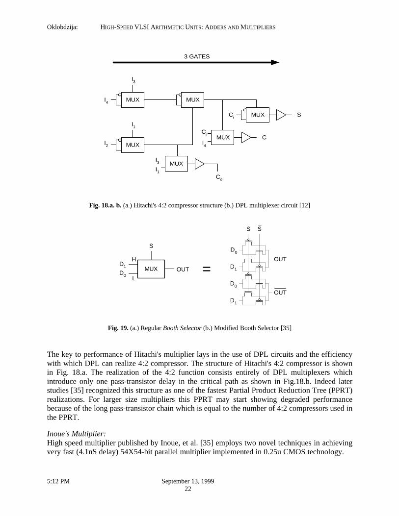
Fig. 19. (a.) Regular Booth Selector (b.) Modified Booth Selector [35] The key to performance of Hitachi's multiplier lays in the use of DPL circuits and the efficiencywith which DPL can realize 4:2 compressor. The structure of Hitachi's 4:2 compressor is shownin Fig. 18.a. The realization of the 4:2 function consists entirely of DPL multiplexers whichintroduce only one pass-transistor delay in the critical path as shown in Fig.18.b. Indeed laterstudies [35] recognized this structure as one of the fastest Partial Product Reduction Tree (PPRT)realizations. For larger size multipliers this PPRT may start showing degraded performancebecause of the long pass-transistor chain which is equal to the number of 4:2 compressors used inthe PPRT. Inoue's Multiplier:High speed multiplier published by Inoue, et al. [35] employs two novel techniques in achievingvery fast (4.1nS delay) 54X54-bit parallel multiplier implemented in 0.25u CMOS technology.
MUX
MUX
MUX
MUX
I4
I3
I1
I2
MUX
MUX
I1
I3
I4
Ci
Ci
Co
C
S
3 GATES
L
H
MUX
D0
D1
D0
D1
S S
OUT
OUT
OUT
S
D1
D0

Oklobdzija: HIGH-SPEED VLSI ARITHMETIC UNITS: ADDERS AND MULTIPLIERS
5:12 PM September 13, 199923
The first novelty introduced is in a new design of the Booth Encoder and Booth selector forgeneration of partial products. The encoding used in Inoue's multiplier is shown in Table 2.
Table 2: Truth Table for Second-Order Modified Booth Encoding [35]
There are two bits used for generation of sign of the partial product: Mj (for negative) and PLj(for positive). Though, this may seem to be redundant at the first sight, it allows for a simplerimplementation of the Booth Encoder which does not require an XOR gate in the critical path.The equations for Booth Selector using regular and modified Booth Encoding are listed:
jjijiji MXaXaP ⊕⋅+⋅= − )2( 1, 2)-n 4,-n0,2,4,...,j 1-n,0,1,2,....(i ==
.....regular Booth Encoder(a.)
jjijijjijiji XMaPLaXMaPLaP ⋅⋅⋅+⋅+⋅+⋅= −− 2)()( 11, 2)-n 4,-n0,2,4,...,j 1-n,0,1,2,....(i ==
....... Modified Booth Encoder(b.)
A modified equations (b.) obtained from the Table 2. yield simpler Booth Selectorimplementation than the regular case. Modified Booth Selector is shown in Fig. 19. (b.) versusregular Booth Selector shown in Fig. 19. (a.).
0 0 0
0 0 1
0 1 0
0 1 1
1 0 0
1 0 1
1 1 0
1 1 1
0 0 0
1 0 0
1 0 0
0 1 0
0 1 1
1 0 1
1 0 1
0 0 1
0
1
1
1
0
0
0
0
0
0
0
0
0
+A
+A
+2A
-A
-A
0
Xj
Inputs Usual Sign select
Func. 2Xj Mj Xj 2Xj MjPLjbj+1 bj bj-1
-2A
0
1
1
0
0
1
1
0
1
0
0
1
0
0
1
1
1
1
1
0
Xj - partial product , PLj - positive partial product, Mj - negative partial product
B - Multiplier (encoded), A - Multiplicand,
P = AxB

Oklobdzija: HIGH-SPEED VLSI ARITHMETIC UNITS: ADDERS AND MULTIPLIERS
5:12 PM September 13, 199924
Fig. 19. (a.) Regular Booth Selector (b.) Modified Booth Selector [35]
The modified Booth Selector requires 10 transistors per bit as compared to the regular BoothSelector which requires 18 transistors per bit for its implementation. The modification shown inTable 2. yields 44% reduction in the transistor count for the Booth Selector of the 54X54-bitmultiplier. Given that the total number of transistor used for Booth Encoder in a 54X54-bitmultiplier is only 1.2% of the total, modification of the Booth Encoder resulting from the Table2. does not result in significant transistor savings. However, the use of the new Booth Encoderresulted in a slight improvement in speed.
The second novelty in Inoue's multiplier is the pass-transistor implementation of the 4:2compressor, which is shown in Fig. 20.
Inoue realized that there are 26 possible implementations of the 4:2 compressor. Out of the totalnumber of 26 they have chosen the one that yields the minimal transistor count yet maintainingthe speed within the 5% of the fastest possible realization. This resulted in 24% savings intransistor count in the partial product reduction tree as compared to the earlier designs [34]. Thetransistor savings more than offset the 5% speed degradation by yielding more area and powerefficient design. It could be argued that the area improvement resulted in a better speed in thefinal implementation, which the simulation tools were not able to show.
Mj
aiXjai-12Xj
Pi,j
ConventionalBooth selector
Sign select SE
L
SE
L
SE
L
SE
L
ai ai ai-1ai-1
Pi,j Pi-1,j
XjXj
Xj
PLj
Mj
ei,j
ei-2,j
new 2-bit combinedBooth selector
10 Tr./bit
18 Tr./bit
- 8 Tr./bit
(a.)
(b.)

Oklobdzija: HIGH-SPEED VLSI ARITHMETIC UNITS: ADDERS AND MULTIPLIERS
5:12 PM September 13, 199925
Fig. 20. Pass-Transistor Implementation of the 4:2 Compressor [35]
XORCin
C
S
Co
X1X2
X3
X4
X1X2
X3X4
Co
C
S
Cin
60 Tr.
48 Tr.
0.49ns
0.45ns(-8.9%)
Delay @2.5V
4:2 CompressorCircuitry (625 cells)
Conventional
This work

Oklobdzija: HIGH-SPEED VLSI ARITHMETIC UNITS: ADDERS AND MULTIPLIERS
5:12 PM September 13, 199926
Conclusion
In the past, a thorough examination of the algorithms with the respect to particular technologyhas only been partially done. The merit of the new technology is to be evaluated by its ability toefficiently implement the computational algorithms. In the other words, the technology isdeveloped with the aim to efficiently serve the computation. The reverse path; evaluating themerit of the algorithms should also be taken. Therefore, it is important to develop computationalstructures that fit well into the execution model of the processor and are optimized for the currenttechnology. In such a case, optimization of the algorithms is performed globally across thecritical path of its implementation.Ability to integrate 100 millions of transistors onto the silicon has changed our focus and theway we think. Measuring the quality of the algorithm by the minimum number of devices usedhas simply vanished from the picture. However, new concerns such as power, have entered it.

Oklobdzija: HIGH-SPEED VLSI ARITHMETIC UNITS: ADDERS AND MULTIPLIERS
5:12 PM September 13, 199927
References
[1] A. Avizienis, “Digital Computer Arithmetic: A Unified Algorithmic Specification”,Symposium on Computers and Automata, Polytechnic Institute of Brooklyn, April 13-15,1971.
[2] Earl E. Swartzlander, “Computer Arithmetic” Vol. 1 & 2, IEEE Computer Society Press,1990.
[3] K. Hwang, "Computer Arithmetic : Principles, Architecture and Design", John Wiley andSons, 1979.
[4] S.Waser, M.Flynn, “Introduction to Arithmetic for Digital Systems Designers”, Holt,Rinehart and Winston 1982.
[5] M. Ercegovac, “Digital Systems and Hardware/Firmware Algorithms”, Chapter 12:Arithmetic Algorithms and Processors, John Wiley & Sons, 1985.
[6] T. Kilburn, D.B.G. Edwards and D. Aspinall, Parallel Addition in Digital Computers: A NewFast "Carry" Circuit, Proc. IEE, Vol.106, Pt.B. p.464, September 1959.
[7] V.G. Oklobdzija, E.R. Barnes, “Some Optimal Schemes for ALU Implementation in VLSITechnology”, Proceedings of 7th Symposium on Computer Arithmetic, June 4-6, 1985,University of Illinois, Urbana, Illinois.
[8] V. G. Oklobdzija, “Simple And Efficient CMOS Circuit For Fast VLSI Adder Realization,”Proceedings of the International Symposium on Circuits and Systems, pp. 1-4, 1988.
[9] C. Nagendra, et al, “A Comparison of the Power-Delay Characteristics of CMOS Adders”,Proceedings of the International Workshop on Low-Power Design, 1994.
[10] Yano, K, et al, "A 3.8 ns CMOS 16x16-b Multiplier Using Complementary Pass-TransistorLogic," IEEE Journal of Solid-State Circuits, vol. 25, pp. 388-395, April 1990.
[11] M. Suzuki et al, "A 1.5nS 32b CMOS ALU in Double Pass-Transistor Logic", Digest ofTechnical Papers, 1993 IEEE Solid-State Circuits Conference, San Francisco, February 24-26, 1993.
[12] N. Ohkubo, et al, “A 4.4-ns CMOS 54x54-b Multiplier Using Pass-transistor Multiplexer”,Proceedings of the Custom Integrated Circuits Conference, San Diego, California, May 1-4,1994.
[13] Weinberger, J.L. Smith, “A Logic for High-Speed Addition”, National Bureau of Standards,Circulation 591, p. 3-12, 1958.
[14] Naini, D. Bearden, W. Anderson, “A 4.5nS 96-b CMOS Adder Design”, IEEE 1992 CustomIntegrated Circuits Conference, 1992.
[15] B.D. Lee, V.G. Oklobdzija, “Improved CLA Scheme with Optimized Delay”, Journal ofVLSI Signal Processing, Vol. 3, p. 265-274, 1991.
[16] Kogge, P.M., Stone, H.S., “A Parallel Algorithms for the Efficient Solution of a GeneralClass of Recurrence Equations”, IEEE Transactions on Computers, Vol. C-22, No 8, Aug.1973. p. 786-93.
[17] A. Bilgory and D.D. Gajski, Automatic Generation of Cells for Recurence Structures, Proc.of 18th Design Automation Conference, Nashville, Tennessee, 1981.
[18] Brent, R.P.; Kung, H.T. A regular layout for parallel adders. IEEE Transactions onComputers, vol.C-31, (no.3), March 1982. p.260-4.

Oklobdzija: HIGH-SPEED VLSI ARITHMETIC UNITS: ADDERS AND MULTIPLIERS
5:12 PM September 13, 199928
[19] H. Ling, “High Speed Binary Adder”, IBM Journal of Research and Development, Vol. 25,No 3, May 1981. p. 156.
[20] Naffziger, S., “A Sub-Nanosecond 0.5 um 64 b Adder Design”, 1996 IEEE InternationalSolid-State Circuits Conference, Digest of Technical Papers, San Francisco, February 8-10,1996. p. 362-3.
[21] Sklanski, “Conditional-Sum Addition Logic”, IRE Transaction on Electronic Computers,EC-9, pp. 226-231, 1960.
[22] O. J. Bedrij, "Carry-Select Adder", IRE Transaction on Electronic Computers, June 1962.[23] D. Dobberpuhl et al, “A 200MHz 64-b Dual-Issue CMOS Microprocessor”, IEEE Journal
of Solid-State Circuits, Vol 27, No 11. November 1992.[24] S. D. Pezaris "A 40 ns 17-bit array multiplier", IEEE Trans. on Computers., Vol. C-20, pp.
442-447, Apr. 1971.[25] C.S. Wallace, “A Suggestion for a Fast Multiplier”, IEE Transactions on Electronic
Computers, EC-13, p.14-17, 1964.[26] L. Dadda, “Some Schemes for Parallel Multipliers”, Alta Frequenza, Vol.34, p.349-356,
March 1965.[27] W. J. Stenzel, "A Compact High Speed Parallel Multiplication Scheme", IEEE Transaction
on Computers, Vol. C-26, pp. 948-957, February 1977.[28] A. Weinberger, “4:2 Carry-Save Adder Module”, IBM Technical Disclosure
Bulletin.,Vol.23, January 1981.[29] J. Fadavi-Ardekani, "M x N Booth Encoded Multiplier Generator Using optimized Wallace
Trees" IEEE trans. on VLSI Systems, Vol. 1 ,No.2, June 1993.[30] V.G. Oklobdzija, D. Villeger, S. S. Liu, “A Method for Speed Optimized Partial Product
Reduction and Generation of Fast Parallel Multipliers Using and Alghoritmic Approach”,IEEE Transaction on Computers, Vol. 45, No 3, March 1996.
[31] A. D. Booth, "A Signed Binary Multiplication Technique", Qarterly J. Mechan. Appl.Math., Vol. IV, 1951.
[32] O. L. Mac Sorley, "High Speed Arithmetic in Binary Computers", Proceedings of IRE,Vol.49, No. 1, January, 1961.
[33] Ohkubo, N., Suzuki, M., Shinbo, T., Yamanaka, T., Shimizu, A.; Sasaki, K., Nakagome, Y.,“A 4.4 ns CMOS 54*54-b Multiplier using Pass-Transistor Multiplexer”, IEEE Journal ofSolid-State Circuits, Vol. 30, No 3, March 1995. p. 251-7.
[34] G. Goto, et al., “A 4.1nS Compact 54X54-b Multiplier Utilizing Sign-Select BoothEncoders”, IEEE Journal of Solid-State Circuits, Vol. 32, No 11, November 1997. p. 1676-82.
[35] A. Inoue, R. Ohe, S. Kashiwakura, S. Mitari, T. Tsuru, T. Izawa, G. Goto, "A 4.1nSCompact 54X54b Multiplier Utilizing Sign Select Booth Encoders", 1997 IEEE InternationalSolid State Circuits Conference, Digest of Papers, San Francisco, 1997. p.416.
[36] M. Nagamatsu et al, "A 15nS 32X32-bit CMOS Multiplier with an Improved ParallelStructure", Digest of Technical papers, IEEE Custom Integrated Circuits Conference 1989.
[37] P. Stelling, C. Martel, V. G. Oklobdzija, R. Ravi, “Optimal Circuits for ParallelMultipliers,” IEEE Transaction on Computers, Vol. 47, No.3, pp. 273-285, March, 1998.
[38] C. Mead, L. Conway, "Introduction to VLSI systems", Addison-Wesley, 1980.


![Chapter 11 · 2. COMPARISON OF VLSI ADDERS The most common approach in comparing VLSI adders was to use of a single delay point [1,2]. An example of such comparison (based only on](https://img.dokumen.tips/doc/110x75/5f44fd1856be9f2faa76e1d7/chapter-11-2-comparison-of-vlsi-adders-the-most-common-approach-in-comparing-vlsi.jpg)