Embed Size (px)
Citation preview
University of Massachusetts Dartmouth
Department of Electrical and Computer Engineering
Design and Fabrication of a Microfluidic Flow Rate and Temperature Sensor
A Thesis in
Electrical Engineering
by
Justin P. McKennon
Submitted in Partial Fulfillment of the
Requirements for the Degree of
Master of Science
January 2014

I grant the University of Massachusetts Dartmouth the non-exclusive right to use the work for the purpose of making single copies of the work available to the public on a not-for-profit basis if the University’s circulating copy is lost or destroyed.
____________________________________
Justin P. McKennon
Date _______________________________

We approve the thesis of Justin P. McKennon
Date of Signature
________________________________________ __________________
David Rancour Associate Professor of Electrical and Computer Engineering Thesis Advisor ________________________________________ __________________ Jonathan Rothstein Associate Professor of Mechanical and Industrial Engineering University of Massachusetts Amherst Thesis Committee ________________________________________ __________________ Gaurav Khanna Associate Professor of Physics Thesis Committee ________________________________________ __________________ Dayalan Kasilingam Professor and Chairperson Department of Electrical and Computer Engineering Thesis Committee ________________________________________ __________________ Karen Payton Graduate Program Director Department of Electrical and Computer Engineering ________________________________________ __________________ Robert Peck Dean, College of Engineering ________________________________________ __________________ Tesfay Meressi Associate Provost for Graduate Studies and Research Development

iii
Abstract
Design and Fabrication of a Microfluidic Flow Rate and Temperature Sensor
by Justin P. McKennon
The field of microfluidics has been an emerging area of popular research in the fields of
science and engineering since it first emerged in the early 1980s. Residing at the
intersection of engineering, chemistry, physics, and biology, microfluidics problems have
posed some of the greatest challenges of science in recent times. Due to the extreme
difficulty in manipulating, measuring, and controlling the fluid volumes and velocities
associated with microfluidics applications, many significant scientific advances have
been held out of reach. Of the all the bottlenecks associated with microfluidics, the
accurate measurement and characterization of fluids in these systems has proven to be
one of the most challenging. Sensors in this category are constrained to geometrically
minute spaces, typically on the sub-millimeter scale, making conventional measurement
techniques obsolete for many applications.
Despite the difficulties associated with developing microfluidic devices, progress
continues to be made in many important areas. One of these areas deals with the
development of lab-on-a-chip devices. These devices integrate one or several laboratory
functions onto a single chip and deal with the handling and manipulation of extremely
small volumes of fluids. One essential function of these types of devices is the ability to
measure the flow rate and temperature of the fluid in the device. This thesis discusses the
methods and techniques associated with exploiting the unique electrical and thermal
properties of Barium Strontium Titanate (BaSrTiO3) in order to develop a simultaneous
flow rate and temperature sensor for use in microfluidic applications.
Through the use of the COMSOL Multiphysics modeling suite, several sensor models are
simulated. Results obtained from these simulations are very promising and allow for both
temperature and flow to be accurately reconciled from sensor readouts. Using these
simulated results as a basis for design, actual sensors are fabricated. The real data
obtained from the fabricated sensors agrees very well with the simulated data.
Differences between the simulated and actual data occur due to the presence of
background noise in the actual data. The analytical methods used to obtain flow rate and
temperature values from the sensor readouts are discussed in this thesis, as well as the
techniques used to etch and cut the desired designs on the physical sensors.

iv
Acknowledgements
I would like to thank all my peers and professors that have helped me reach this point in
my academic career.
Many thanks go to my advisor, Dr. David Rancour. His patience, technical expertise, and
guidance have proven invaluable in every facet of my research, and without him none of
this would have been possible.
I would also like to thank my committee member Dr. Jonathan Rothstein, for his
collaboration throughout this project and for serving on my committee.
Additionally, I would like to thank Dr. Gaurav Khanna and Dr. Dayalan Kasilingam for
their roles and effort in helping me throughout the research process, as well as for serving
on my committee. I would also like to extend thanks to the University of Massachusetts
Dartmouth Advanced Technology Manufacturing Center for generously allowing me the
use of their facilities throughout my research.
Last but not least, I would like to thank my mom, my fiancée Jill, and my big brother Ed.
Their personal guidance and support has long been what has propelled me to further my
education, and for this I am forever grateful.

v
Table of Contents
List of Figures vi
Chapter One - Introduction 2
Chapter Two - Sensor A1 3
2.1 Theory of Operation 4
2.2 A1 Sensor Characterization 5
2.3 Governing Physics 8
2.4 A1 Simulation 10
2.5 A1 Design Enhancement 13
2.6 Enhanced A1 Design Analysis 19
Chapter Three - Sensor Fabrication 24
3.1 Patterning 24
3.2 Etching 28
3.3 Channel Cutting 32
Chapter Four - Real A1 Data 38
4.1 Data Analysis 38
Chapter Five - Conclusion 44
References 45

vi
List of Figures
Figure 2.1 Resistance versus Temperature for BaSrTiO3 4
Figure 2.2 Proposed TWIA sensor architecture A1 5
Figure 2.3 Proposed A1 sensor architecture 6
Figure 2.4 Actual A1 Fabricated Architecture 7
Figure 2.5 COMSOL generated mesh for A1 model 10
Figure 2.6 A1 Inlet and outlet pad regression surfaces 11
Figure 2.7 Inlet and outlet pad contours 12
Figure 2.8 Sensor A1 flow-temperature readout plot, for high-flow region only 13
Figure 2.9 A1 electric potential 14
Figure 2.10 A1 electric potential, bottom surface 15
Figure 2.11 A1 Current density during operation 16
Figure 2.12 Enhanced A1 sensor design with back contact removed 17
Figure 2.13 Electric potential with back contact removed 18
Figure 2.14 Horizontal slice of current density 19
Figure 2.15 Inlet and Outlet pad regression surfaces for the enhanced A1 design 20
Figure 2.16 Inlet and outlet contours for the enhanced A1 design 21
Figure 2.17 Regression surface queries for enhanced A1 design 22
Figure 2.18 Regression surface queries at low flow 23
Figure 3.1 Actual size of an un-etched BaSrTiO3 tablet 25
Figure 3.2 Laser-cut PCB stencil mask 26
Figure 3.3 A1 patterning style 1 27
Figure 3.4 Crystalline form of Ferric Nitrate 28
Figure 3.5 Ideal etching solution 29
Figure 3.6 Conductive silver epoxy 31
Figure 3.7 Wired sensor 32
Figure 3.8 IX-300 laser 33
Figure 3.9 Metallic staging 34
Figure 3.10 Inspection camera 35
Figure 3.11 Process camera 36
Figure 3.12 Scanning electron microscope image of channel after 3 runs of the cutting
macro 37
Figure 4.1 Contour plot for 1-30µL/min flow rates 39
Figure 4.2 Interpolation surface queries for 1-30 µL/min flow rates 41
Figure 4.3 Contour plot for low flow region 412
Figure 4.4 Surface queries for the low flow region 423

2
Chapter One - Introduction
The field of microfluidics has continued to be one of the fastest expanding areas of
research in science and technology in recent years. In 2010, the microfluidics industry
was estimated to be worth $3.2 billion. By 2015, the microfluidics industry is projected to
constitute a $12 billion market [1]. As both government agencies and private
organizations continue to heavily invest in microfluidics research and development, this
number will only continue to increase. However, despite these investments in research,
there are still many questions that are without answers.
At such geometrically small sizes, the modeling and development of sensors and devices
has proven to be an enormous challenge. At these scales, the sheer complexity of the
governing mathematics and physics is a tremendous bottleneck in research. In addition to
the theoretical hurdles, the physical manipulation and characterization of fluids and
particles at this scale rests on the edge of the current capabilities of science. However, in
spite of these difficulties, many significant advancements have been made throughout the
field.
One of the most active areas of research in microfluidics deals with the development and
implementation of lab on a chip technology. Long considered the holy grail of
microfluidics, lab on a chip technologies require the integration of various key
technologies onto a single chip. By combining these sensors into a single cohesive
system, the cost and time associated with performing these functions can be drastically
reduced. The medical field stands as a shining example of an area of science that lab on a
chip technology will benefit. By implementing a successful lab on a chip system, many
essential medical functions can be performed simultaneously. This will not only reduce
the costs related with performing these functions, but it will also considerably decrease
the time required to obtain results.
In nearly all permutations of lab on a chip devices, an essential functionality of the
system is to be able to easily and accurately measure the flow rate and temperature of the
fluid in question. Many research groups have developed ways to achieve this. Cole and
Kenis [2] have developed a sensor capable of measuring flow velocities as low as 111 x
10-3 cm/s. Mizuno et al have developed sensors capable of measuring velocities as low as
125 x 10-3 cm/s [3]. Chiang et al have created sensors capable of measuring flow rates as
low as 0.37 x 10⁻³ cm/s [4]. Fang and Tan have implemented a sensor capable of
resolving flow rates as low as 8.4 x 10⁻³ cm/s [5]. TWIA has developed a macroscopic
sensor capable of measuring flow velocities as low as 68.4 x 10⁻³ cm/s [6]. Although
these flow velocities are extremely low, many applications require additional flow
sensitivity. TWIA's current macroscopic sensor is the only sensor that allows for the
3
measurement of flow and temperature at the same time. All of the reported groups
achieved low flow velocities with microscopic devices, while TWIA accomplished this
with a macroscopic sensor. By miniaturizing their macroscopic sensor, the flow
sensitivity of TWIA’s sensor will increase, all while maintaining the ability to measure
temperature simultaneously. This research will focus on the design, simulation, and
development of improved microscopic sensor designs derived from TWIA's initial
sensor.
While simulated data can provide considerable developmental insight, relying solely on
this information can cause misleading conclusions to be drawn. Ultimately, simulated
data is limited by the accuracy and performance of the software used to generate the data.
The COMSOL Multiphysics suite is widely regarded as one of the most accurate and
powerful software tools used in computer aided design and simulation exercises. Through
the use of this software package and associated toolboxes, an accurate representation of
the sensor functionality can be obtained. The mathematics used in these simulations
represents the best method by which science is able to explain the phenomena that occur
during the actual operation of the sensor. However, even when generated through tools
such as COMSOL, synthetic data still doesn't provide a perfect representation of real
world sensor functionality. These software simulations provide a template for what the
expected performance of a sensor will be, but real-world experiments in the presence of
noise and environmental factors will ultimately allow for a proper conclusion as to the
performance of a given sensor. This research will develop an analytical method for
numerically determining the accuracy in terms of flow rate and temperature sensing for a
sensor.
Using simulation data as a baseline for a sensor performance does have its advantages.
Fabricating and testing real sensors is both costly and time consuming, thus, software
provides a validation test to determine whether a sensor should or should not be built.
Coupling the simulation process with the fabrication process has proven to be an
extremely effective method from both a cost and time standpoint. Through various
iterations of this process, an improved sensor can be developed. This research focuses on
TWIA's current A1 sensor and developing a new architecture that addresses the issues
associated with its design. The following chapter focuses on A1’s theory of design and
the development of a model to be used in simulation. Chapter three describes a new
sensor architecture and analyzes its performance. Chapter four explains the fabrication
process associated with producing an actual sensor to be used in experiments, and chapter
five presents and analyzes the experimental data from this design. As a final point, a
conclusion on the overall sensor performance is given, along with some discussion of
future work.

4
Chapter Two – Sensor A1
2.1 Theory of Operation
TWIA's current sensor operates as an extremely sensitive hot-wire anemometer. Their
sensor exploits the very strong positive temperature coefficient of resistance of Barium
Strontium Titanate (BaSrTiO3). Figure 2.1 illustrates that near its curie temperature,
BaSrTiO3 demonstrates an increasing resistance versus temperature characteristic.
Figure 2.1 Resistance versus Temperature for BaSrTiO3
As a voltage is applied to the sensor, an electric field is created. This field accelerates the
electrons as they travel through the ceramic. The electrons lose small amounts of their
kinetic energy as they collide with the atomic ions of the BaSrTiO3. The transfer of this
kinetic energy through vibrations in the lattice creates heat. This heat not only causes the
temperature of the sensor to increase, but also the electrical resistance. In steady state and
under a constant voltage bias, the sensor stabilizes at a point where
� = � ∗ �(�)
in which V represents sensor voltage, I is sensor current, and R is sensor resistance as a
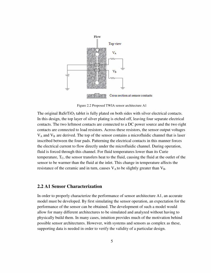
function of temperature. In figure 2.2, the A1 sensor architecture is shown [5].
5
Figure 2.2 Proposed TWIA sensor architecture A1
The original BaSrTiO3 tablet is fully plated on both sides with silver electrical contacts.
In this design, the top layer of silver plating is etched off, leaving four separate electrical
contacts. The two leftmost contacts are connected to a DC power source and the two right
contacts are connected to load resistors. Across these resistors, the sensor output voltages
VA and VB are derived. The top of the sensor contains a microfluidic channel that is laser
inscribed between the four pads. Patterning the electrical contacts in this manner forces
the electrical current to flow directly under the microfluidic channel. During operation,
fluid is forced through this channel. For fluid temperatures lower than its Curie
temperature, TC, the sensor transfers heat to the fluid, causing the fluid at the outlet of the
sensor to be warmer than the fluid at the inlet. This change in temperature affects the
resistance of the ceramic and in turn, causes VA to be slightly greater than VB.
2.2 A1 Sensor Characterization
In order to properly characterize the performance of sensor architecture A1, an accurate
model must be developed. By first simulating the sensor operation, an expectation for the
performance of the sensor can be obtained. The development of such a model would
allow for many different architectures to be simulated and analyzed without having to
physically build them. In many cases, intuition provides much of the motivation behind
possible sensor architectures. However, with systems and sensors as complex as these,
supporting data is needed in order to verify the validity of a particular design.
6
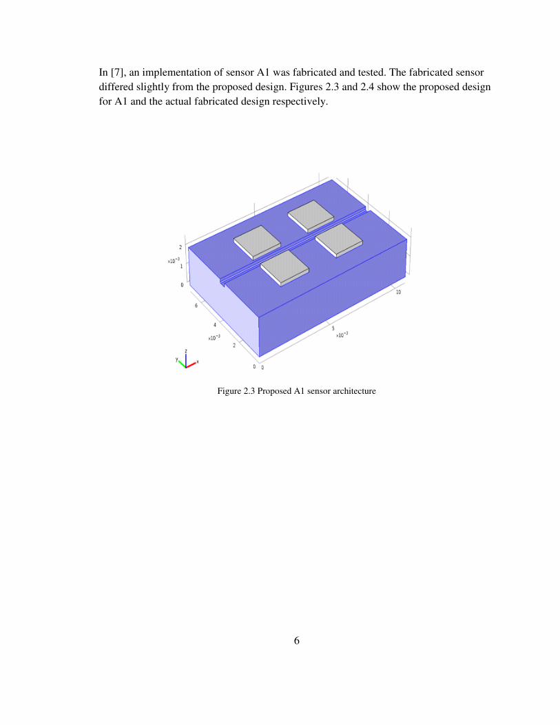
In [7], an implementation of sensor A1 was fabricated and tested. The fabricated sensor
differed slightly from the proposed design. Figures 2.3 and 2.4 show the proposed design
for A1 and the actual fabricated design respectively.
Figure 2.3 Proposed A1 sensor architecture

7
Figure 2.4 Actual A1 Fabricated Architecture
Unlike the original design, both the top and bottom surfaces of the tablet are metal plated.
The actual fabricated sensor metallization is only about 28 µm thick, whereas in our
COMSOL simulation model we used a 200 µm metallization thickness. Also, the
simulated sensors had microfluidic channels running the entire length of the tablet, but
the fabricated sensors’ channels spanned about 77% of the tablet’s length. These changes
were used to keep the finite element problem more manageable for COMSOL, but do not
affect the qualitative results of the simulations.
The overall dimensions of the A1 sensor changed from the proposed model to the
fabricated sensor. The physical size and shape of the dimensions is determined by GE,
the supplier of the BaSrTiO3 tablets. In the fabricated design, the overall dimensions of
the sensor are 11.05mm×7.4mm×2mm. The channel is 0.64mm wide by 0.2mm deep.
8
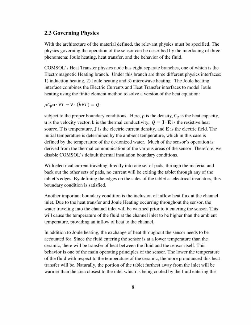
2.3 Governing Physics
With the architecture of the material defined, the relevant physics must be specified. The
physics governing the operation of the sensor can be described by the interfacing of three
phenomena: Joule heating, heat transfer, and the behavior of the fluid.
COMSOL’s Heat Transfer physics node has eight separate branches, one of which is the
Electromagnetic Heating branch. Under this branch are three different physics interfaces:
1) induction heating, 2) Joule heating and 3) microwave heating. The Joule heating
interface combines the Electric Currents and Heat Transfer interfaces to model Joule
heating using the finite element method to solve a version of the heat equation:
�u ∙ ∇� − ∇ ∙ (�∇�) = �,
subject to the proper boundary conditions. Here, ρ is the density, Cp is the heat capacity,
u is the velocity vector, k is the thermal conductivity, � = J ∙ E is the resistive heat
source, T is temperature, J is the electric current density, and E is the electric field. The
initial temperature is determined by the ambient temperature, which in this case is
defined by the temperature of the de-ionized water. Much of the sensor’s operation is
derived from the thermal communication of the various areas of the sensor. Therefore, we
disable COMSOL’s default thermal insulation boundary conditions.
With electrical current traveling directly into one set of pads, through the material and
back out the other sets of pads, no current will be exiting the tablet through any of the
tablet’s edges. By defining the edges on the sides of the tablet as electrical insulators, this
boundary condition is satisfied.
Another important boundary condition is the inclusion of inflow heat flux at the channel
inlet. Due to the heat transfer and Joule Heating occurring throughout the sensor, the
water traveling into the channel inlet will be warmed prior to it entering the sensor. This
will cause the temperature of the fluid at the channel inlet to be higher than the ambient
temperature, providing an inflow of heat to the channel.
In addition to Joule heating, the exchange of heat throughout the sensor needs to be
accounted for. Since the fluid entering the sensor is at a lower temperature than the
ceramic, there will be transfer of heat between the fluid and the sensor itself. This
behavior is one of the main operating principles of the sensor. The lower the temperature
of the fluid with respect to the temperature of the ceramic, the more pronounced this heat
transfer will be. Naturally, the portion of the tablet furthest away from the inlet will be
warmer than the area closest to the inlet which is being cooled by the fluid entering the

9
channel. This will cause a temperature gradient across the sensor, thus affecting the
resistance accordingly.
The behavior of the fluid traveling through the channel also has plays a role in the
performance of the sensor. The Reynolds number characterizes the line that separates
laminar and turbulent flows. [7] claims that the critical Reynolds number corresponding
to the onset of turbulent flow is Re ≈ 2300, whereas TWIA’s microfluidic flow sensors
have Re values < 1 thus laminar flow can be assumed. In addition, due to the extremely
low volume of fluid traveling through the channel, the inertial component of the Navier-
Stokes equations can be ignored, allowing for the fluid to be accurately modeled as a
creeping flow. At the boundaries of the microfluidic channel, a no-slip condition is
applied. This condition implies that at the interface of the fluid and the sides of the
channel itself, the tangential component of the fluid velocity must be continuous. At such
low volumes of fluid, the density of the fluid itself can be viewed as constant and thus,
the flow itself is characterized as isochoric or incompressible.
Since COMSOL’s simulation results are obtained through the use of a finite element
method, a mesh needs to be developed for the model. COMSOL allows the user to be
able to define their own mesh and associated parameters, or implement a physics defined
mesh. In A1, the majority of the physical phenomena are occurring in the areas closest to
the channel. Therefore, considerably more computation effort is required to evolve the
behavior of the sensor in those areas, justifying the use of employing a physics defined
mesh. In figure 2.5, the mesh used for sensor A1 is shown. Note how around the channel
the mesh becomes considerably denser.

10
Figure 2.5 COMSOL generated mesh for A1 model
2.4 A1 Simulation
With an appropriately defined sensor model, simulations were conducted. A 50V bias
was applied to the sensor during this run. Additionally, in order to fully characterize the
operation of the sensor, both the flow rate and temperature of the fluid need to be varied
during the simulation.
In this case, the fluid’s flow rate was swept from 1-500 µL/min. The simulation consisted
of these flow sweeps at 0C, 5C, 10C, 15C, and 20C respectively. In doing so, the
performance of the sensor can be analyzed over its entire operating range. For each flow
rate and temperature value, the output current at each set of pads was measured. This
allows for the inlet pad current and outlet pad current to be determined as a function of
flow and temperature.
In flow temperature space, each inlet pad and outlet pad current is unique and can be
associated with a specific flow-rate and temperature. When the inlet and outlet pad
currents are plotted over the entire range of flow-rates and temperatures used in the
simulation, these data points can be fit to a regression surface. The crossings of the
contours of these surfaces in flow temperature space correspond to what the sensor would
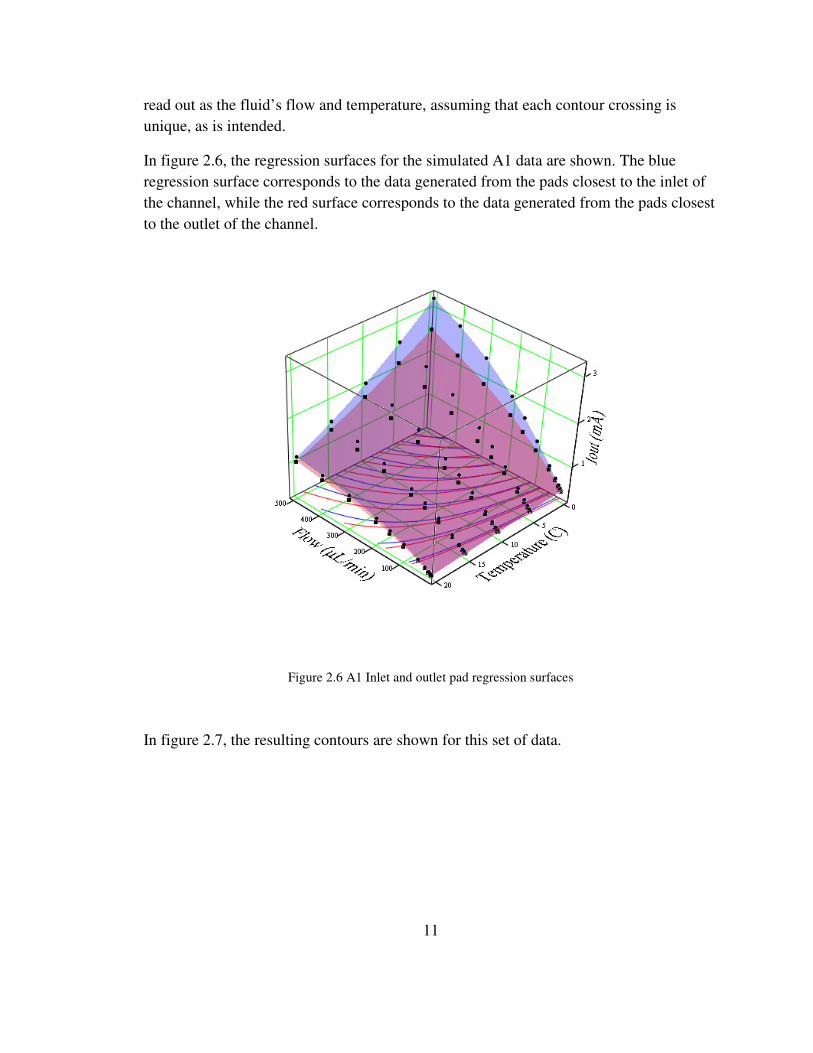
11
read out as the fluid’s flow and temperature, assuming that each contour crossing is
unique, as is intended.
In figure 2.6, the regression surfaces for the simulated A1 data are shown. The blue
regression surface corresponds to the data generated from the pads closest to the inlet of
the channel, while the red surface corresponds to the data generated from the pads closest
to the outlet of the channel.
Figure 2.6 A1 Inlet and outlet pad regression surfaces
In figure 2.7, the resulting contours are shown for this set of data.
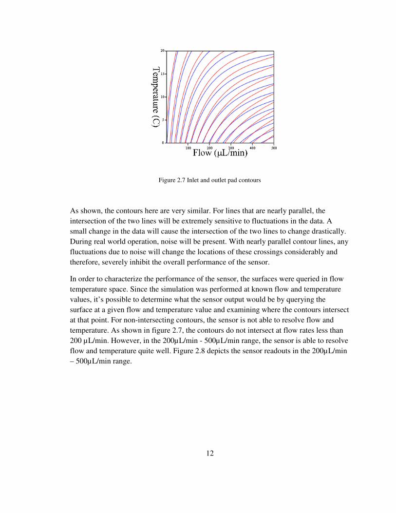
12
Figure 2.7 Inlet and outlet pad contours
As shown, the contours here are very similar. For lines that are nearly parallel, the
intersection of the two lines will be extremely sensitive to fluctuations in the data. A
small change in the data will cause the intersection of the two lines to change drastically.
During real world operation, noise will be present. With nearly parallel contour lines, any
fluctuations due to noise will change the locations of these crossings considerably and
therefore, severely inhibit the overall performance of the sensor.
In order to characterize the performance of the sensor, the surfaces were queried in flow
temperature space. Since the simulation was performed at known flow and temperature
values, it’s possible to determine what the sensor output would be by querying the
surface at a given flow and temperature value and examining where the contours intersect
at that point. For non-intersecting contours, the sensor is not able to resolve flow and
temperature. As shown in figure 2.7, the contours do not intersect at flow rates less than
200 µL/min. However, in the 200µL/min - 500µL/min range, the sensor is able to resolve
flow and temperature quite well. Figure 2.8 depicts the sensor readouts in the 200µL/min
– 500µL/min range.

13
Figure 2.8 Sensor A1 flow-temperature readout plot, for high-flow region only
In this flow region, A1 had an RMS flow error of 1.4% and an RMS temperature error of
1.7%. While the sensor performs extremely well over this operating range, the desired
operating range is considerably lower. The degradation in performance at lower flow
rates is due to the similarity in shape between the inlet and outlet contours. At lower
flows, the cooling effect of the water on the tablet is diminished. This causes the inlet and
outlet of the tablet to behave very similarly, and thus cause their contours to be close to
identical in shape.
2.5 A1 Design Enhancement
As previously mentioned, the operating principle behind sensor A1 was to have the
electric current flow directly under the microfluidic channel. With the current traveling
directly under the channel, maximum flow sensitivity can be obtained. In flowing directly
under the channel, direct heat transfer between the sensor and the fluid will occur.

14
After the initial simulations of A1 were conducted, an interesting observation was made.
As shown in figure 2.4, A1 has metal surfaces on both the top and bottom of the tablet.
Examining the electric potential of the tablet from the initial A1 simulation produced
figure 2.9.
Figure 2.9 A1 electric potential
As shown, the bottom metallic surface is held at one half of the applied voltage during
operation. Rotating the above image to focus on the bottom contact creates figure 2.10.

15
Figure 2.10 A1 electric potential, bottom surface
It turns out that the metal on the bottom of the tablet acts as an equipotential surface
during operation. This skews the operation of the sensor and causes the majority of the
electric current to travel along this surface as it moves through the tablet, far away from
the microfluidic channel. Figure 2.11 depicts this phenomenon.

16
Figure 2.11 A1 Current density during operation
With the back contact acting as an equipotential surface, the sensor is not operating as it
was intended to. In order to eliminate this behavior the back metal contact was removed,
producing figure 2.12, the enhanced design of A1, shown with the PDMS cap attached.

17
Figure 2.12 Enhanced A1 sensor design with back contact removed
With the back contact removed from the substrate, the equipotential surface no longer
exists. After re-simulating the architecture and examining the electric potential across the
tablet, it can be verified that the equipotential surface no longer is present during
operation, as shown in figure 2.13.

18
Figure 2.13 Electric potential with back contact removed
Furthermore, without the presence of an equipotential surface, the current can now travel
directly under the channel as desired. Figure 2.14 illustrates a horizontal slice of the
current density with proportional arrows indicating flow of current.

19
Figure 2.14 Horizontal slice of current density
2.6 Enhanced A1 Design Analysis
Although the removal of the back contact has forced the sensor to behave as intended, it
is not readily obvious that the ability of the sensor to resolve both flow and temperature
will improve.
Using fourth order polynomial regression, the inlet and outlet pad currents were fit to
regression surfaces and mapped into flow-temperature space, producing figure 2.15.

20
Figure 2.15 Inlet and Outlet pad regression surfaces for the enhanced A1 design
As shown, the surfaces still show a high degree of similarity in terms of their shape. The
contours are less similar than they were prior to the removal of the back contact, which is
a welcome sign. Due to scaling, the contours here appear to be non-intersecting.
However, as shown in figure 2.16, this is not the case.

21
Figure 2.16 Inlet and outlet contours for the enhanced A1 design
Figure 2.16 verifies that the contours are indeed intersecting to a much higher degree than
they were prior to the removal of the back contact. Querying the regression surfaces
produces figure 2.17.

22
Figure 2.17 Regression surface queries for enhanced A1 design
The removal of the back contact has removed the non-intersecting contour behavior from
the sensor. Prior to this, the sensor was only able to work for larger flow rates (>200
µL/min). With the desired operating region being at very low flow rates, Figure 2.18
paints a very promising picture.

23
Figure 2.18 Regression surface queries at low flow
Over the entire flow region of 1-100 µL/min, the sensor performs remarkably well. The
RMS flow error is 1.923% and the RMS temperature error is .769%. These values prove
that with this design, the sensor is able to simultaneously resolve both flow and
temperature, and produce values that are more than 98% accurate. With such a high
degree of accuracy, there is considerable motivation to fabricate and test the sensor in a
real world environment.
24
Chapter Three – Sensor Fabrication
3.1 Patterning
Off the shelf, the original BaSrTiO3 tablets come fully plated on both sides with silver.
Much of the operating characteristics of the sensor are determined by the size, location,
and patterning of the electrical contacts. Thus, to physically fabricate the A1 architecture
onto the tablet, the silver plating needs to be removed from some areas of the ceramic and
kept in other areas. While there are numerous methods for performing such a task, the
easiest and most appropriate method for removing the silver from the tablet can be done
through a process called etching.
Typically, etching can be separated into two main types; wet and dry etching. Wet
etching is the process by which the metal on a given material is dissolved or removed
chemically. Dry etching is performed when material is sputtered or dissolved using
reactive ions or a vapor phase etchant. Due to the availability of materials and costs
associated with each process, wet etching was used to remove the metal from the tablet.
During wet etching, the material is completely submerged in the etchant. Since there is a
need for the silver to remain in some areas, a suitable etch resist needs to be applied to
the areas where silver is to remain. In order to prevent the solution from dissolving the
silver over the desired pad areas, the resist needs to bond appropriately to the silver and
act as an intermediary between the etchant and the silver itself. Finding a suitable
substance to do this can be a challenging task. However, in the case of silver, indelible
ink performs extremely well as a resist.
Indelible ink is generally comprised of a resin, a colorant, a pyrrolidone, a carrier solvent
and a glyceride [8]. The combination of these substances allows for the ink to remain
largely waterproof, although the ink itself is not truly permanent. On hard non-porous
surfaces, the ink does not actually stain the surface as desired. Instead, the ink forms a
surface layer that is resistant to removal, but not immune to it. Ink of this type can be
removed by submerging the ink covered area into an agitated acetone bath. This makes
indelible ink ideal for this application.
While indelible ink works as a resist to the ferric nitrate and water etch solution, seeping
around the edges of the silver and marker boundary still occurs. As a result, truly straight
edges are difficult to create. Additionally, due to the physical size between the tip of the
marker and the size of the tablet, patterning becomes a considerable challenge. Figure 3.1
shows an actual un-etched BaSrTiO3 tablet in comparison to a penny.

25
Figure 3.1 Actual size of an un-etched BaSrTiO3 tablet
For the case of the BaSrTiO3 tablet, an etching mask was created to alleviate many of the
maneuverability issues associated with drawing the desired pattern on the substrate itself.
The mask itself was made from a laser cut PCB stencil. The stencil itself was cut to have
a variety of pad sizes available to maximize its versatility as shown in figure 3.2.

26
Figure 3.2 Laser-cut PCB stencil mask
Using an ultra fine tipped sharpie, the areas where silver is to remain were colored in.
Two versions of the sensor were patterned. The first pattern is shown in figure 3.3.

27
Figure 3.3 A1 patterning style 1
This pattern differs slightly from the simulated design but is qualitatively identical. The
four pads were patterned to be slightly smaller to allow for more non-plated area to
surround the eventual microfluidic channel. The PDMS is easier to apply with a larger
work area around the channel and ultimately, this allows for a better seal over the
channel.
The second patterned sample was an identical match to the simulated architecture. The
pads are slightly larger and the etched area surrounding the eventual microfluidic channel
is slightly smaller. The sensor itself was originally cut and etched to be an A1 sample
with the back contact still attached and here, the back contact was simply removed.
Additionally, prior to applying the marker to pattern the substrates, each substrate was
submerged in an agitated acetone bath. This was done to remove any oils and residue
from the silver plating. If this step is skipped, the ink itself would bond to the oils and
impurities resulting in the ink forming a surface layer on the oils themselves as opposed
to the tablets. Then, when the tablet is submerged in the etching solution, the ink will not

28
have properly bonded to the tablets and the etching solution will dissolve the silver
around the edge of the desired area, if not the entire area.
3.2 Etching
One of the most commonly used etching mixtures for the removal of silver is Ferric
Nitrate. Ferric Nitrate is a strong oxidant and irritant but is not able to dissolve indelible
ink, making it ideal for this application. In solid form, shown in figure 3.4, Ferric Nitrate
is a violet crystal and is readily soluble in many liquids.
Figure 3.4 Crystalline form of Ferric Nitrate
Ferric nitrate is typically classified as a slow-etching material. This means that the
chemical reaction that occurs when in the presences of a reactive material is non-
aggressive making it safe for standard lab use.
Due to the physical size of the tablets, the amount of actual etching solution needed is
minimal. For best results, the tablet need only be completely submerged, although if
multiple tablets are to be etched in a single solution, more liquid is required. This is due
to the fact that as the silver is dissolved in the etching solution, it becomes polluted with
silver particulate. This reduces the potency and reactivity of the solution and causes the

29
etching process to slow. In a properly saturated solution, the silver particulates are
essentially diffused throughout the etchant making it possible to etch many tablets with
one batch of the solution.
The typical ratio of Ferric Nitrate to water used is 10-15g of Ferric Nitrate for every
50mL of water. The amount of Ferric Nitrate differs depending on the consistency of the
water it is being mixed with. Depending on the source of the water, it may contain
various minerals that will slightly inhibit the saturation of the overall solution, causing
more Ferric Nitrate to be needed to have a sufficiently strong etching solution.
In general, the proper amount of Ferric Nitrate can be determined by the color of the
etching solution itself. As previously mentioned, in solid form, Ferric Nitrate appears as a
violet crystal. When added to water, the Ferric Nitrate reacts with the water and turns a
yellowy orange color. As more Ferric Nitrate is added, the etching solution darkens. The
ideal etching solution will be very dark orange, as shown in figure 3.5.
Figure 3.5 Ideal etching solution
Also shown in figure 3.5 is the plastic tubing coming from the agitator. When preparing
to etch, it is essential to ensure that the Ferric Nitrate is uniformly distributed throughout

30
the etching solution. Doing so ensures that the etching will occur evenly regardless of
where in the solution the tablet resides. In this case, an Aquatic Gardens 800 single-outlet
aquarium pump was used to agitate the solution. This pump provided sufficient
circulation without causing the solution to bubble over or spill out of the container.
Once the etching solution has been agitated for a few minutes, the cleaned and patterned
tablet can be submerged in the solution. Using a set of locking plastic vice-pliers, the
tablet can be suspended in the solution, allowing for the simultaneous etching of both
sides of the tablet. With an appropriately saturated solution, the etching process takes
roughly 25 minutes to complete. After removing the tablet from the etching solution it
will appear as if the silver is still on the tablet. However, the etching process dissolves the
bond between the ceramic and the silver plating in the non marked areas and easily wipes
off with a towel. Once the silver residue has been wiped away, the tablet needs to be
submerged in a cleansing, cold water bath to stop the etching process. From here, the
tablet can then be dipped into an agitated acetone bath for several minutes to remove the
patterning ink.
While the indelible ink is sufficiently resistant to the etching solution, it does wear off
over time. As previously mentioned, the ink does not actually stain the silver itself. It
forms a surface layer on the silver and is thus susceptible to coming off. With the Ferric
Nitrate particles in the etching solution being agitated, the solution itself acts as a dull
friction brush on the surface of the tablet. After about 10 minutes in the solution the
patterned area may appear faded or lighter. When this happens, the tablet needs to be
cleaned in the cold water ice bath, dried, and re-patterned to ensure that the silver plating
in the desired locations is not removed. The re-patterning does not require placing the
tablet in the acetone bath, merely re-applying the ink to the desired areas.
After successfully removing the tablets from the etching solution and halting the etching
process, wires need to be bonded to each of the pads. Again, prior to attaching anything
to the tablet, each etched tablet needs to be submerged in an agitated acetone bath. This
ensures that any remaining ink is removed from the tablets along with any oils and
residue. With the tablets free of any contaminants, each pad then needs to be scuffed with
a steel wool sponge. This makes the surface of the pads rougher and will prevent the
wires from sliding along the surface while bonded.
During previous rounds of testing, the wires were soldered to each of the pads. However,
soldering requires extremely high temperatures that often damage the ceramic. These
temperatures weaken the tablets and can cause them to crack or shatter entirely. To
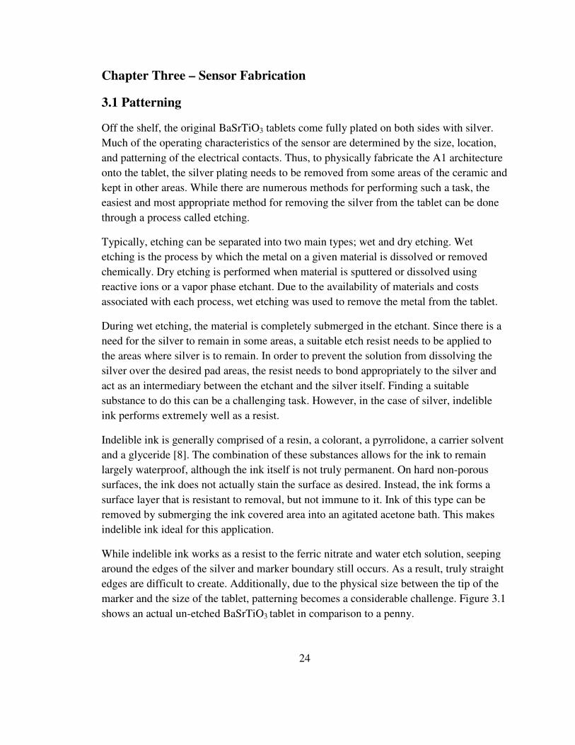
alleviate this issue, the wires were attached with a conductive silver epoxy, as shown in
figure 3.6.
31
Figure 3.6 Conductive silver epoxy
The high silver content of the epoxy allows for low resistance, durable, and electrically
conductive bonds to be formed without the potential for damaging the tablet due to the
heat shock commonly caused by soldering. The epoxy has a typical pot time on the order
of 10-15 minutes and a cure time of 20 minutes once it has set. An image of one of the
sensors wired up with the epoxy is shown in figure 3.7. Flexible, thin-gauge wire was
used here. Heavier gauge wire, when bent, creates an enormous amount of torque on the
epoxy and was liable to strip the silver plating right off of the tablet itself. The thin gauge
allowed for the wiring to be manipulated for packaging, transport, and operation without
fear of breaking the electrical connection and damaging the tablet.
32
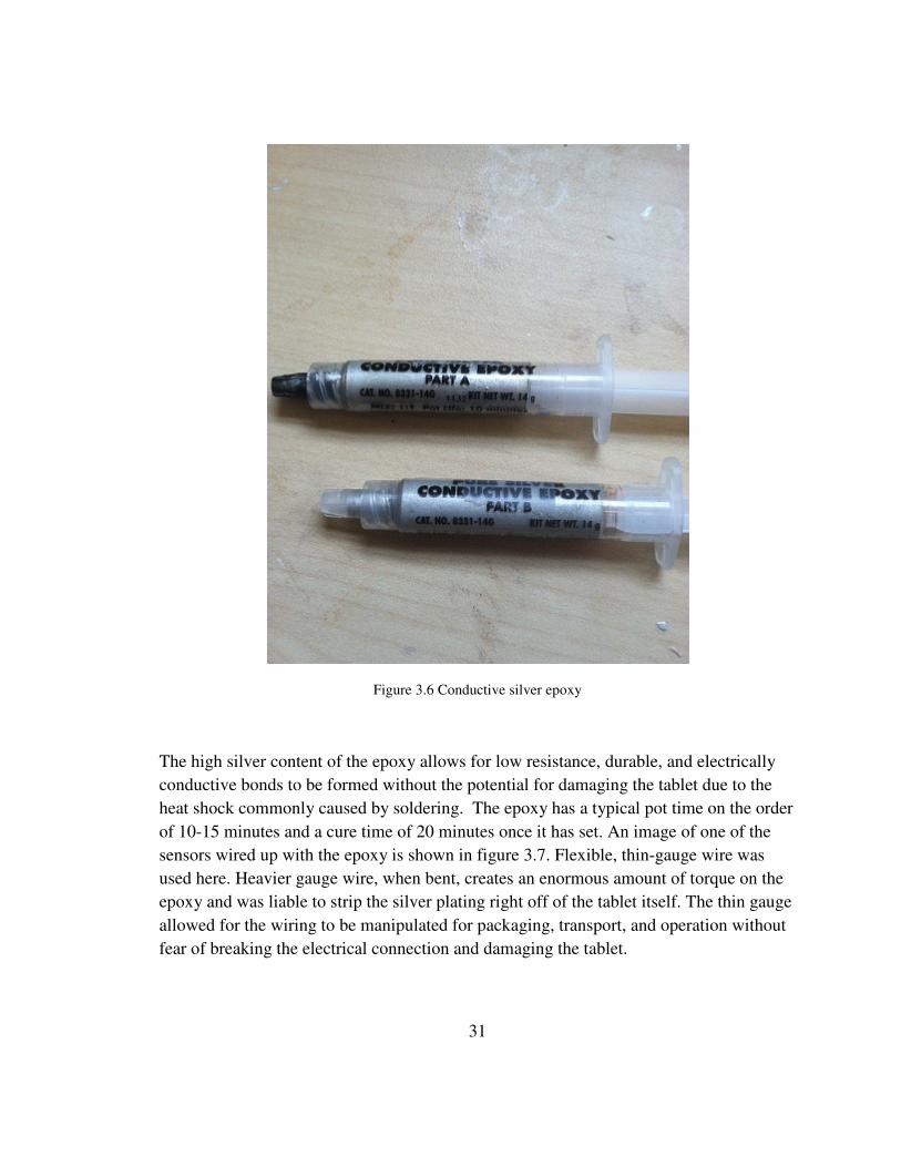
Figure 3.7 Wired sensor
As shown, the epoxy covers a good portion of the surface area of the pads. In order to
obtain a good seal with the PDMS cover, adequate room on both sides of the pads is
required as well as a flat surface for the PDMS to adhere to. This prevents the PDMS
from getting into the channel and isolates the channel from contaminants. In addition, the
seal is a vital part of the performance of the sensor as it allows for the fluid itself to be
forced through the channel appropriately.
3.3 Channel Cutting
Before the tablet can be sealed with the PDMS, the channel itself needs to be cut. For
larger sensors, mechanically cutting the channel into the tablet would be appropriate.
However on the millimeter scale, this becomes very impractical. Thus, to appropriately
carve a channel into the tablet, it must be micromachined with a laser.
In 2005, the University of Massachusetts-Dartmouth Advanced Technology
Manufacturing Center acquired an IX-300 ultraviolet laser micromachining system from
JP Sercel and Associates Inc. The IX-300 was specifically designed to allow for the
creation of micron-scale features with tolerances of less than a micron, making it ideal for

33
the fabrication of microfluidic channels. The IX-300, partially shown in figure 3.8, has a
steep learning curve with respect to operation, but is easily accessible and was used in the
fabrication process.
Figure 3.8 IX-300 laser
The IX-300 is an excimer laser. Lasers of this type produce light through a chemical
reaction involving an excited dimer. Excited dimers are dimeric or heterodimeric
molecules formed from two atoms, one of which is in an excited electron state [9].
Excimer lasers have long been in use for a variety of medical applications, the most
famous of which is LASIK eye surgery. The lifetime of an excited dimer is very short,
forcing the laser to operate through pulses.
Before operating the laser, the gases used to form the actual laser need to be filled. Stale
gases in the laser cause the energy of the laser to deteriorate, minimizing the
effectiveness of the laser and drastically increasing the time it takes to cut the channel.
The minimum required energy to cut the channel is 60mJ. The upper limit for the desired
operating power is 75mJ, as any further added energy is liable to burn the tablet.
With fresh gas inside the laser, the part to be cut needs to be appropriately staged. During
operation, there are many moving parts within the laser. The channel needs to be
precisely inscribed on the tablet, making it desirable to securely fasten the tablet to
prevent any undesired movement. The metallic staging platform is shown in figure 3.9.
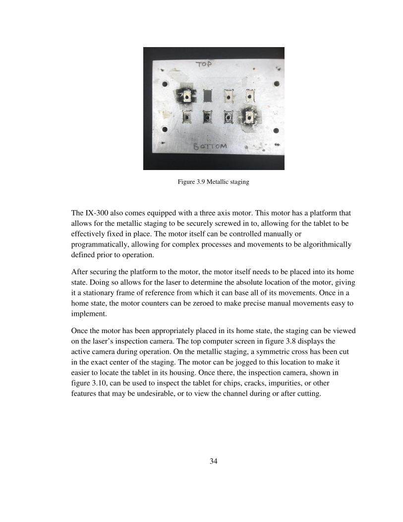
34
Figure 3.9 Metallic staging
The IX-300 also comes equipped with a three axis motor. This motor has a platform that
allows for the metallic staging to be securely screwed in to, allowing for the tablet to be
effectively fixed in place. The motor itself can be controlled manually or
programmatically, allowing for complex processes and movements to be algorithmically
defined prior to operation.
After securing the platform to the motor, the motor itself needs to be placed into its home
state. Doing so allows for the laser to determine the absolute location of the motor, giving
it a stationary frame of reference from which it can base all of its movements. Once in a
home state, the motor counters can be zeroed to make precise manual movements easy to
implement.
Once the motor has been appropriately placed in its home state, the staging can be viewed
on the laser’s inspection camera. The top computer screen in figure 3.8 displays the
active camera during operation. On the metallic staging, a symmetric cross has been cut
in the exact center of the staging. The motor can be jogged to this location to make it
easier to locate the tablet in its housing. Once there, the inspection camera, shown in
figure 3.10, can be used to inspect the tablet for chips, cracks, impurities, or other
features that may be undesirable, or to view the channel during or after cutting.
35
Figure 3.10 Inspection camera
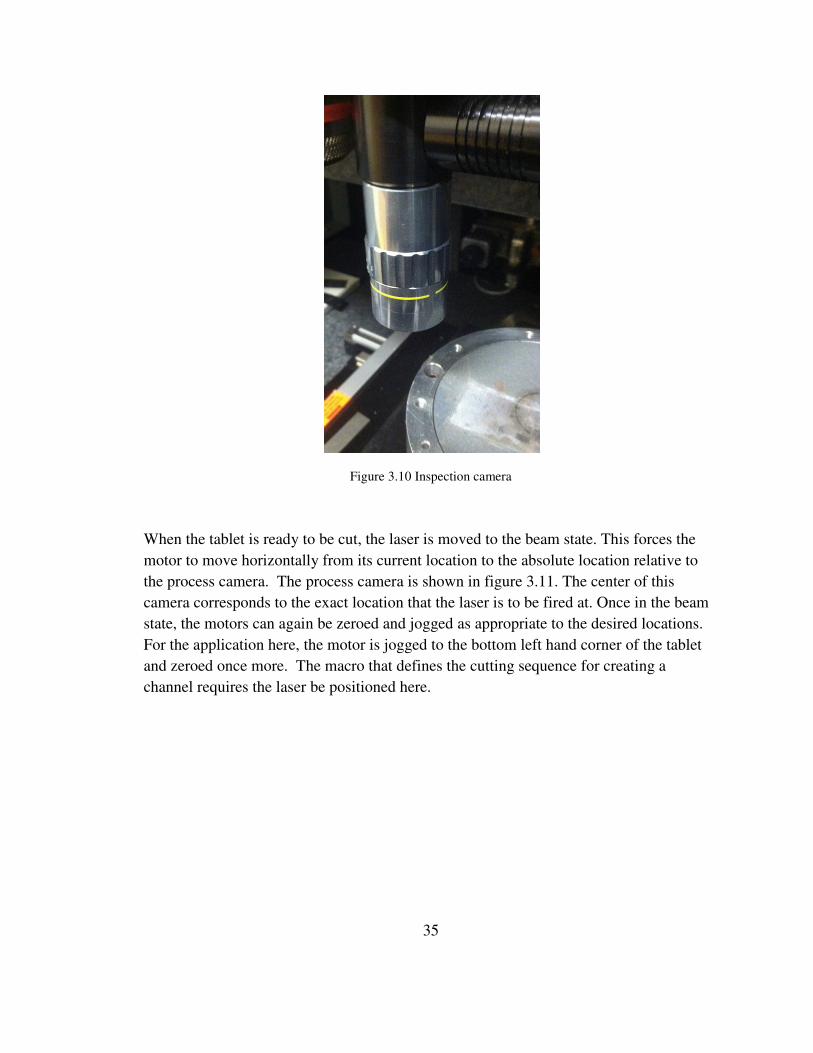
When the tablet is ready to be cut, the laser is moved to the beam state. This forces the
motor to move horizontally from its current location to the absolute location relative to
the process camera. The process camera is shown in figure 3.11. The center of this
camera corresponds to the exact location that the laser is to be fired at. Once in the beam
state, the motors can again be zeroed and jogged as appropriate to the desired locations.
For the application here, the motor is jogged to the bottom left hand corner of the tablet
and zeroed once more. The macro that defines the cutting sequence for creating a
channel requires the laser be positioned here.

36
Figure 3.11 Process camera
The physical shape of the beam emitted from the laser during operation can be controlled
by varying the size and shape of the mask. For this application, a square mask was used.
This mask produces square pulses that are 600 microns wide. The actual depth of the cut
produced by each pulse of the laser varies greatly from operation to operation. The
energy of the beam and the composition of the tablet play a large role in this factor. Thus,
the channel itself is cut in several steps. The cutting macro moves the motor into the
appropriate position and fires the laser. The motor is stepped by exactly the length of the
square imprint created by the laser. This is continued until the desired channel length has
been reached. At this point, the laser begins stepping backwards in a similar fashion to
the starting point. The macro repeats this process many times. In order to achieve the
desired channel depth of 200 µM, the macro needs to be re-run many times. After a few
iterations of the macro, it is wise to measure the depth of the channel with the inspection
camera. After roughly three iterations of the macro, the channel should be close to 10µM
deep and resemble figure 3.11, although much wider. Note that figure 3.11 was produced
with a different mask on the laser to create a thinner beam pattern, but the laser intensity
was identical to that used to cut the channel with the larger mask. This caused the width
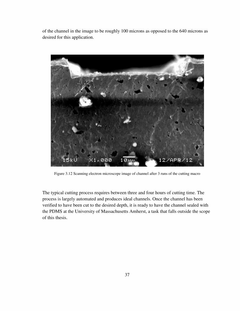
37
of the channel in the image to be roughly 100 microns as opposed to the 640 microns as
desired for this application.
Figure 3.12 Scanning electron microscope image of channel after 3 runs of the cutting macro
The typical cutting process requires between three and four hours of cutting time. The
process is largely automated and produces ideal channels. Once the channel has been
verified to have been cut to the desired depth, it is ready to have the channel sealed with
the PDMS at the University of Massachusetts Amherst, a task that falls outside the scope
of this thesis.

38
Chapter Four – Real A1 Data
4.1 Data Analysis
With the sensor etched, cut, and sealed, experimental data was taken. Data points were
obtained at five separate temperatures, 4.2°C, 5.6°C, 8.5°C, 11.5°C, and 14.4°C, and six
separate flow rates, 1 µL/min, 5µL/min, 10 µL/min, 20 µL/min, 40 µL/min, and 80
µL/min. At each temperature and flow rate, the sensor was allowed to reach steady state
prior to any flow being applied. With the sensor at steady state, flow was applied to the
channel for five minutes before taking each data point to ensure that the sensor was in
steady state.
With data points at only six separate flow rates, it is difficult to accurately characterize
the performance of the real A1 sensor. To alleviate this issue, 2 dimensional interpolation
was performed on the sparse data to obtain a more dense set of values for analysis. Using
MATLABs interpolation routines, data points were obtained at 2 µL/min, 3 µL/min, 4
µL/min, 6 µL/min, 7 µL/min, 8 µL/min, 9 µL/min, 15 µL/min, 30 µL/min, 50 µL/min, 60
µL/min, and 70 µL/min. This increases the number of flow rates for analysis from six to
eighteen in total.
As with any experiment, the sensor measurements are subject to a variety of sources of
noise. While every attempt was made to accurately replicate the A1 design, imperfections
in the BaSrTiO3 compared to the simulated model are present as well, due in part to the
physical make up of the tablet, as well as the imperfections in the channel dimensions
from the laser, and pad sizing from the etching.
The intersection points of the inlet and outlet contours were unable to be obtained for
flow rates greater than 30 µL/min. At these flow rates, the contours intersected multiple
times, making for wildly inaccurate queries of the contour surfaces. This is due in part to
the sensor response itself, and also by the ability of the 3-D interpolation routines to
accurately model the surfaces. When the contours do not intersect, or intersect multiple
times for a given flow and temperature, the interpolation surfaces either cannot be
queried, or produce wildly inaccurate results.
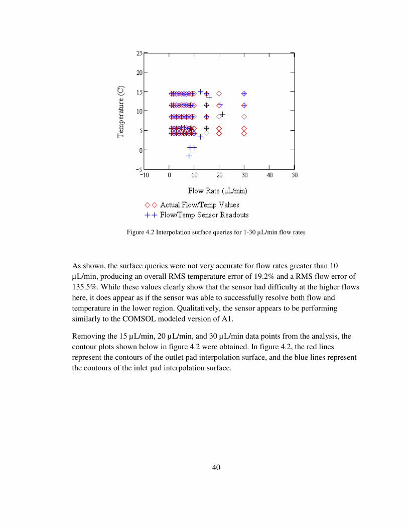
Flow rates 30 µL/min and less allowed for contours to be generated and queried. Shown
below, figure 4.1 displays the contour plots for the flow rates between 1-30 µL/min.

39
Figure 4.1 Contour plot for 1-30µL/min flow rates
As shown, the contours here intersect nicely at each flow-temperature point. While it is
readily evident that both the inlet and outlet pads are responding to changes in flow, the
inlet pads certainly appear to be much more sensitive.
Querying the generated interpolation surfaces produces figure 4.2, shown below.
40
Figure 4.2 Interpolation surface queries for 1-30 µL/min flow rates
As shown, the surface queries were not very accurate for flow rates greater than 10
µL/min, producing an overall RMS temperature error of 19.2% and a RMS flow error of
135.5%. While these values clearly show that the sensor had difficulty at the higher flows
here, it does appear as if the sensor was able to successfully resolve both flow and
temperature in the lower region. Qualitatively, the sensor appears to be performing
similarly to the COMSOL modeled version of A1.
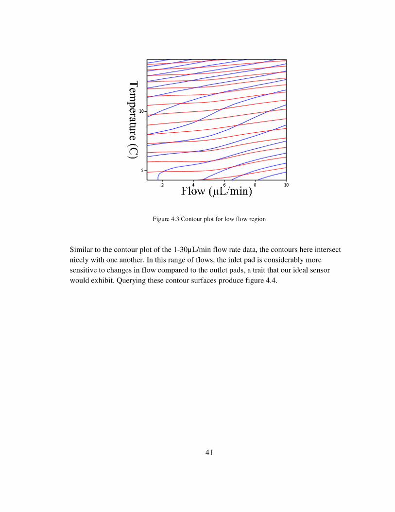
Removing the 15 µL/min, 20 µL/min, and 30 µL/min data points from the analysis, the
contour plots shown below in figure 4.2 were obtained. In figure 4.2, the red lines
represent the contours of the outlet pad interpolation surface, and the blue lines represent
the contours of the inlet pad interpolation surface.
41
Figure 4.3 Contour plot for low flow region
Similar to the contour plot of the 1-30µL/min flow rate data, the contours here intersect
nicely with one another. In this range of flows, the inlet pad is considerably more
sensitive to changes in flow compared to the outlet pads, a trait that our ideal sensor
would exhibit. Querying these contour surfaces produce figure 4.4.
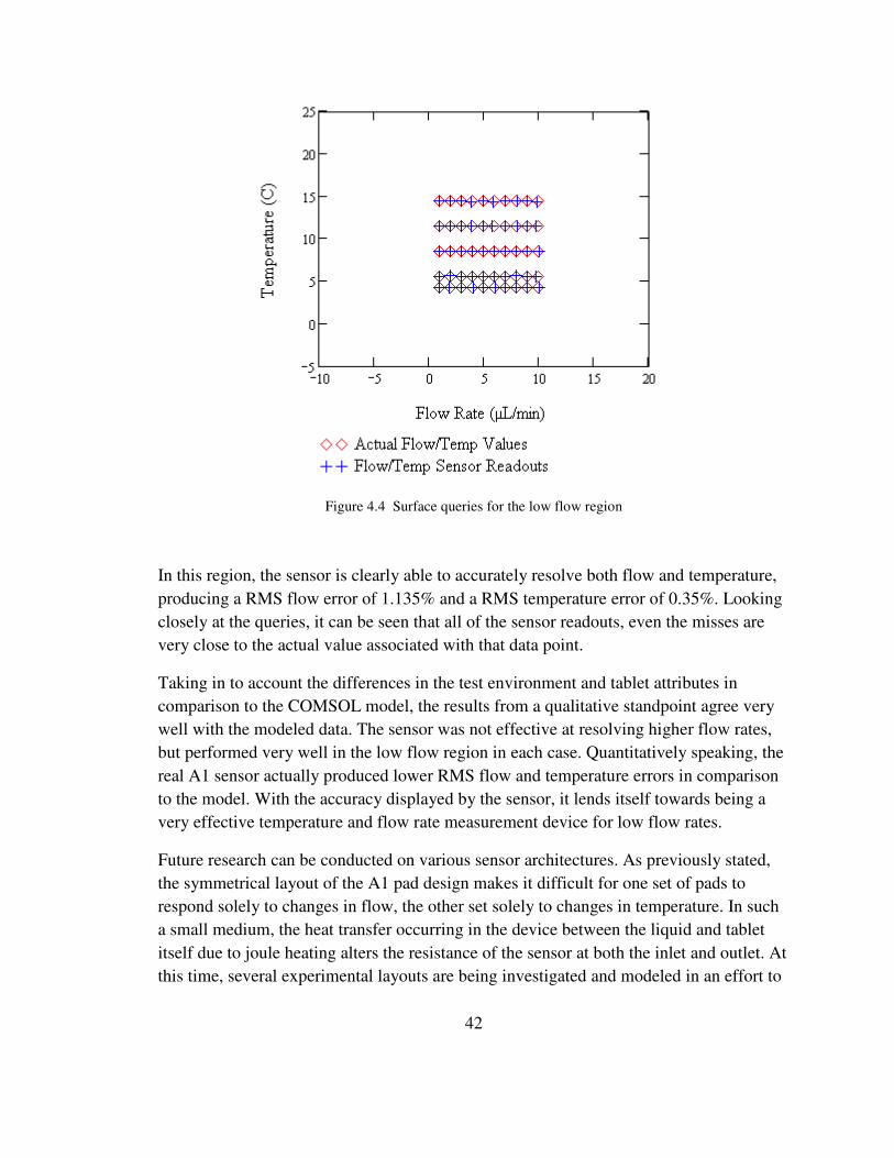
42
Figure 4.4 Surface queries for the low flow region
In this region, the sensor is clearly able to accurately resolve both flow and temperature,
producing a RMS flow error of 1.135% and a RMS temperature error of 0.35%. Looking
closely at the queries, it can be seen that all of the sensor readouts, even the misses are
very close to the actual value associated with that data point.
Taking in to account the differences in the test environment and tablet attributes in
comparison to the COMSOL model, the results from a qualitative standpoint agree very
well with the modeled data. The sensor was not effective at resolving higher flow rates,
but performed very well in the low flow region in each case. Quantitatively speaking, the
real A1 sensor actually produced lower RMS flow and temperature errors in comparison
to the model. With the accuracy displayed by the sensor, it lends itself towards being a
very effective temperature and flow rate measurement device for low flow rates.
Future research can be conducted on various sensor architectures. As previously stated,
the symmetrical layout of the A1 pad design makes it difficult for one set of pads to
respond solely to changes in flow, the other set solely to changes in temperature. In such
a small medium, the heat transfer occurring in the device between the liquid and tablet
itself due to joule heating alters the resistance of the sensor at both the inlet and outlet. At
this time, several experimental layouts are being investigated and modeled in an effort to

43
determine the ideal sensor pad geometry. Additionally, making use of BaSrTiO3 in thin-
film applications may prove to yield a more robust sensor.

44
Chapter Five - Conclusion
Research in the field of microfluidics has been rapidly increasing over the past decade.
With the goal of many of these research endeavors being associated with the
development of lab on a chip technology, the need to accurately characterize and resolve
both flow and temperature is present in many of these such projects.
TWIA has developed a macroscopic sensor capable of resolving both flow rate and
temperature using tablets of BaSrTiO3. By removing portions of the silver plating on the
surface of the tablet and applying a bias across the remaining silver on the sensor, current
can be forced through the sensor. Varying the patterns of the silver plating on the sensor
alters the behavior of the current flowing through the tablet, and thus, the response of the
sensor to changes in flow and temperature.
In this work, the A1 sensor architecture was simulated in COMSOL and a real A1 sensor
was fabricated. The results of this work were very promising, as the real A1 sensor
performed very well in terms of resolving flow rates and temperatures of the water. The
sensor proved to be very accurate in this application, and the results agreed well with the
simulated data.
Unfortunately, the response of the sensor does not merit production as a real world
sensor. While the contours cross very nicely, the ripples in the contour surfaces indicate
that the sensor readouts are not monotonically increasing. The CSI algorithm used to
generate the surfaces forces splines to pass through all of the data points, causing
undulations in the surfaces. As with any experiment, all of the measurements were
subject to various sources of noise, and limited by the accuracy of the measurement
devices.
Despite being unsuitable for real world applications, the performance of the sensor was
very promising. By varying the architecture of the sensor, and making improvements to
the measurement techniques a sensor suitable for real world applications can be
developed.

45
References
1. “Global biosensors market” . PRWeb.com. Retrieved 11 February 2012. Available:
<http://www.prweb.com/releases/biosensors/medical_biosensors/prweb8067456.htm>.
2. “Multiplexed electrical sensor arrays in microfluidic networks”. Scs.Illinois.edu.
Retrieved 20 March 2012. Available:
<http://www.scs.illinois.edu/kenis/Files/57_SnA_Multiplexed_Sensors_2008.pdf>
3. Mizuno, Y., Liger, M., Tai, Y-C., “Nanofluidic flowmeter using carbon sensing
element”, IEEE MEMS (2004) pp. 322-325.
4. Wang, Y. H., Lee, C. Y., Chiang, C. M., “A MEMS-based air flow sensor with a free-
standing micro-cantilever structure”, Sensors 7 (2007) pp. 2389-2401.
5. Fang T., Tan X. “A novel diaphragm micropump actuated by conjugated polymer
petals: Fabrication, modeling, and experimental results”, Sens. Actuators
A. (2010);158:121–131.
6. Rancour, D.“High throughput point-of-care / in-vitro diagnostics platform”, NIST
Proposal (2009).
7. Rancour, D. “TWIA Sensor A1”, COMSOL Simulations (2012).
8. “Ink composition resistant to solvent evaporation”, PatentStorm.us, Retrieved 12
February 2012. Available:
<http://www.patentstorm.us/patents/7084191/description.html>.
9. Schuocker, D. “Handbook of the Eurolaser Academy”, Springer, ISBN 0-412-81910-
4 (1998).