Embed Size (px)
Citation preview

1
Introduction to Combinational Circuit Design
EXP:1 Design of Logic gates
1.1 Introduction
The purpose of this experiment is to simulate the behavior of several of the basic logic gates
and you will connect several logic gates together to create simple digital model.
1.2 Software tools Requirement
Equipments:
Computer with Modelsim Software
Specifications:
HP Computer P4 Processor – 2.8 GHz, 2GB RAM, 160 GB Hard Disk
Softwares: Modelsim - 5.7c, Xilinx - 6.1i.
1.3 Logic Gates and their Properties
Gate Description Truth Table Logic Symbol Pin Diagram
OR
The output is
active high if any one of
the input is in active high
state, Mathematically,
Q = A+B
O
utput Q
0
1
1
1
AND
The output is
active high only if both
the inputs are in active
high state,
Mathematically,
Q = A.B
O
utput Q
0
0
0
1
2
NOT
In this gate the
output is opposite to the
input state,
Mathematically,
Q = A
O
utput Q
1
0
NOR
The output is
active high only if both
the inputs are in active
low state,
Mathematically,
Q = A+B
O
utput Q
1
0
0
0
NAND
The output is
active high only if any
one of the input is in
active low state,
Mathematically,
Q = A.B
O
utput Q
1
1
1
0
EXOR
The output is
active high only if any
one of the input is in
active high state,
Mathematically,
Q = A B
O
utput Q
0
1
1
0
7486
1.4 Pre lab Questions
What is truth table?
Which gates are called universal gates?
Define HDL?
What is the difference b/w HDL and software language?

3
Define Entity and architecture?
Define identifiers.
A basic 2-input logic circuit has a HIGH on one input and a LOW on the other input, and the
output is HIGH. What type of logic circuit is it?
A logic circuit requires HIGH on all its inputs to make the output HIGH. What type of logic
circuit is it?
Develop the truth table for a 3-input AND gate and also determine the total number of
possible combinations for a 4-input AND gate.
VERILOG Program for Basic Logic Gates
a) AND Gate
Gate Level Model
moduleandgate(x,y,z);
inputx,y;
output z;
and g1(z,x,y);
endmodule
Dataflow Model
moduleanddata(x,y,z);
inputx,y;
output z;
assign z=(x&y);
endmodule
b) OR Gate
Gate Level Model
moduleorgate(x,y,z);
inputx,y;
output z;
or g1(z,x,y);
endmodule
Dataflow Model
moduleordata(x,y,z);
inputx,y;
output z;
assign z=(x^y);
endmodule
C) NOT gate

4
Gate Level Model
modulenotgate(x,y);
input x;
output y;
not g1(y,x);
endmodule
Dataflow Model
modulenotdata(x,y);
input x;
output y;
assign y=~(x);
endmodule
D) NAND gate
Gate Level Model
modulenandgate(x,y,z);
inputx,y;
output z;
nand g1(z,x,y);
endmodule
Dataflow Model
modulenanddata(x,y,z);
inputx,y;
output z;
assign z=~(x&y);
endmodule
E) NOR gate
Gate Level Model
modulenorgate(x,y,z);
inputx,y;
output z;
nor g1(z,x,y);
endmodule
Dataflow Model
modulenordata(x,y,z);
inputx,y;
output z;
assign z=~(x^y);

5
endmodule
F) XOR gate
Gate Level Model
modulexorgate(x,y,z);
inputx,y;
output z;
xor g1(z,x,y);
endmodule
Dataflow Model
modulexordata(x,y,z);
inputx,y;
output z;
assign z=((x&(~y))^((~x)&y));
endmodule
G) XNOR gate
Gate Level Model
modulexnorgate(x,y,z);
inputx,y;
output z;
xor g1(z,x,y);
endmodule
Dataflow Model
modulexnordata(x,y,z);
inputx,y;
output z;
assign z=~((x&(~y))^((~x)&y));
endmodule
1.5 Post lab Questions
What is meant by ports?
Write the different types of port modes.

6
What are different types of architecture modeling?
What are different types of operators?
What is difference b/w <= and := operators?
What is meant by simulation?
How to give the inputs in modelsim software.
1.6 Lab Report
Each individual will be required to submit a lab report. Use the format specified in the "Lab
Report Requirements” document available on the class web page. Be sure to include the
following items in your lab report:
Lab cover sheet with staff verification sign.
Answer the pre-lab questions
Complete VERILOG code design for all logic gates and output signal waveforms
Answer the post-lab questions
1.7 Grading
Pre-lab Work 20 points
Lab Performance 30 points
Post-lab Work 20 points
Lab report 30 points
For the lab performance - at a minimum, demonstrate the operation of all the logic gates to
your staff in-charge
The lab report will be graded as follows (for the 30 points):
VERILOG code for each logic gates 15 points
Output signal waveform for all logic gates and its truth table 15 points

7
EXP:2 Design of Binary Adders
2.1 Introduction
The purpose of this experiment is to introduce the design of simple combinational circuits, in
this case half adders, half subtractors, full adders and full subtractors.
Software tools Requirement
Equipments:
Computer with Modelsim Software
Specifications:
HP Computer P4 Processor – 2.8 GHz, 2GB RAM, 160 GB Hard Disk
Softwares: Modelsim - 5.7c, Xilinx - 6.1i.
Logic Diagram
Figure 2.1 Half adder
Figure 2.2 Full adder

8
Figure 2.3 Half subtracter
Figure 2.4 Full subtracter
Pre lab Questions
What is meant by combinational circuits?
Write the sum and carry expression for half and full adder.
Write the difference and borrow expression for half and full subtractor.
Define component and component instantiation.
What is signal? How it is declared?
What are the different logic state systems in std_logic?
VERILOG Program
Half-adder(Dataflow model)
modulehalfadder(sum,carry,a,b);
outputsum,carry;
inputa,b;
assign sum = a ^ b;
assign carry=a&b;
endmodule
Half-adder(Structural model)
modulehalfadder(sum,carry,a,b);
outputsum,carry;
inputa,b;

9
xor(sum,a,b);
and(carry,a,b);
endmodule
Full-adder(Dataflow model)
modulefulladder(sum,carry,a,b,c);
outputsum,carry;
inputa,b,c;
assign sum = a ^ b^c;
assign carry=(a&b) | (b&c) | (c&a);
endmodule
Full-adder(Structural model)
modulefulladder(sum,carry,a,b,c);
outputsum,carry;
inputa,b,c;
wire m1,m2,m3;
xor(sum,a,b,c);
and(m1,a,b);
and(m2,b,c);
and(m3,c,a);
or(m1,m2,m3);
endmodule
Half-subtractor(Dataflow model)
modulehalfsubt(diff,borrow,a,b);
outputdiff,borrow;
inputa,b;
assign diff = a ^ b;
assign borrow=(~a&b);
endmodule
Half-subtractor(Structural model)
modulehalfsubt(diff,borrow,a,b);
outputdiff,borrow;
inputa,b;
xor(diff,a,b);
and( borrow,~a,b);
endmodule
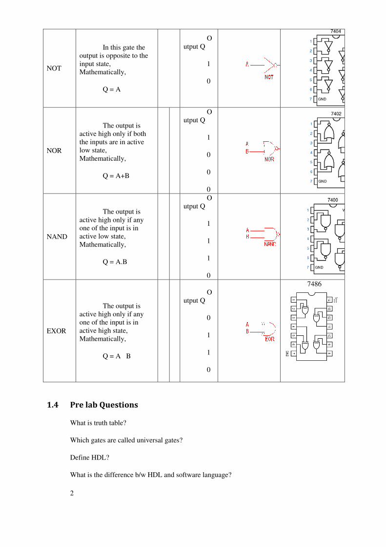
Full-Subtractor (Dataflow model)
modulefullsubt(diff,borrow,a,b,c);
outputdiff,borrow;
inputa,b,c;
assign diff = a ^ b^c;
assign borrow=(~a&b) | (b&c) |
(c&~a);
endmodule
10
Full-Subtractor (Structural model)
modulefullsubt(diff,borrow,a,b,c);
outputdiff,borrow;
inputa,b,c;
wire a0,q,r,s,t;
not(a0,a);
xor(diff,a^b^c);
and(q,a0,b);
and(r,a0,c);
and(s,b,c);
or(t,q,r);
or(borrow,t,s);
endmodule
2.6 Post lab Questions
What are the signal assignment statements?
What are the concurrent statements?
Write short notes on following.
Process statement
Block statement
Write about sequential statements.
What is the difference b/w high impedance state of the signal(Z) and unknown state of the
signal(X).
Lab Report
Each individual will be required to submit a lab report. Use the format specified in the "Lab
Report Requirements” document available on the class web page. Be sure to include the
following items in your lab report:
Lab cover sheet with staff verification sign.
Answer the pre-lab questions
Complete VERILOG code design for all logic gates and output signal waveforms
Answer the post-lab questions

11
Grading
Pre-lab Work 20 points
Lab Performance 30 points
Post-lab Work 20 points
Lab report 30 points
For the lab performance - at a minimum, demonstrate the operation of all the logic gates to
your staff in-charge
The lab report will be graded as follows (for the 30 points):
VERILOG code for each experiments 15 points
Output signal waveform for all experiments and its truth table 15 points

12
Lab 3: Design of Multiplexers and Demultiplexers
3.1 Introduction
The purpose of this experiment is to write and simulate a VERILOG program for
Multiplexers and Demultiplexers.
Software tools Requirement
Equipments:
Computer with Modelsim Software
Specifications:
HP Computer P4 Processor – 2.8 GHz, 2GB RAM, 160 GB Hard Disk
Softwares: Modelsim - 5.7c, Xilinx - 6.1i.
Block Diagram
Figure 3.2 Function Table
Figure 3.1 4:1 Multiplexer Block diagram
Figure 3.3 1:4 Demux Symbol Figure 3.4 Function Table

13
3.4 Logic Diagram
Figure 3.5 4:1 Multiplexer
Figure 3.6 1:4 Demultiplexer Logic

14
Pre lab Questions
Define mux and demux.
Write their applications.
What is the relationship b/w input lines and select lines.
Design 4:1 mux and 1:4 demux.
write brief notes on case statement.
Write the difference b/w if and while statement
3.5 VERILOG Program
Multiplexer:
GATE LEVEL DESCRIPTION OF 2 TO 1 MUX
module multiplexgate2(a,b,s0,y);
input a,b,s0;
output y;
wire net1,net2,net3;
not g1(net1,s0);
and g2(net2,a,s0);
and g3(net3,a,net1);
or g4(y,net3,net2);
endmodule
DATAFLOW DESCRIPTION OF 4 TO 1 MUX
module multiplexer(a,b,c,d,s0,s1,y);
input a,b,c,d,s0,s1;
output y;

15
assign y=((a&(~(s0))&(~(s1)))||(b&(~(s0))&((s1)))||(c&((s0))&(~(s1)))||(d&((s0))&(s1)));
endmodule
DATAFLOW DESCRIPTION OF 8 TO 1 MUX
module mux8to1(y,i,s);
output y;
input [7:0] i;
input [2:0] s;
wire se1;
assign se1=(s[2]*4)|(s[1]*2)|(s[0]);
assign y=i[se1];
endmodule
Demultiplexer
DATAFLOW DESCRIPTION OF 1 TO 4 DEMUX
module demux(in,sel,out)
input in;
input [1:0]sel;
output [3:0]out;
assign out=in<<sel;
endmodule
BEHAVIORAL DESCRIPTION OF 1 TO 8 DEMUX
module demux_1to8(i, sel, y);
input i;
input [2:0] sel;

16
output reg [7:0] y;
always@(i,sel)
begin
y=8'd0;
case(sel)
3'd0:y[0]=i;
3'd1:y[1]=i;
3'd2:y[2]=i;
3'd3:y[3]=i;
3'd4:y[4]=i;
3'd5:y[5]=i;
3'd6:y[6]=i;
default:y[7]=i;
endcase
end
endmodule
3.6 Post Lab questions
Implement the function f(A,B,C)=Σm(0,1,3,5,7) by using Mux.
Write the VERILOG code for the above design
Write the VERILOG code for full subtractor using Demux.
Lab Report
Each individual will be required to submit a lab report. Use the format specified in the "Lab
Report Requirements" document available on the class web page. Be sure to include the
following items in your lab report:
Lab cover sheet with staff verification sign.

17
Answer the pre-lab questions
Complete VERILOG code design for all logic gates and output signal waveforms
Answer the post-lab questions
Grading
Pre-lab Work 20 points
Lab Performance 30 points
Post-lab Work 20 points
Lab report 30 points
For the lab performance - at a minimum, demonstrate the operation of all the logic gates to
your staff in-charge
The lab report will be graded as follows (for the 30 points):
VERILOG code for each experiments 15 points
Output signal waveform for all experiments and its truth table 15 points

18
Lab 4: Design of Encoders and Decoders
Introduction
The purpose of this experiment is to introduce you to the basics of Encoders and Decoders. In
this lab, you have to implement Priority Encoder and the Boolean function using Decoders.
Software tools Requirement
Equipments:
Computer with Modelsim Software
Specifications:
HP Computer P4 Processor – 2.8 GHz, 2GB RAM, 160 GB Hard Disk
Softwares: Modelsim - 5.7c, Xilinx - 6.1i.
Block Diagram
Figure 4.1 4-to-2 bit Encoder
Figure 4.2 2-to-4 Binary Decoders
4.4. Logic Diagram
Figure 4.3 4x2 Decoder

19
Figure 4.4 4x2 Decoder
4.5 Pre lab Questions
What is difference b/w encoder and data selector.
What is the difference b/w decoder and data distributor.
Give the applications of encoder and decoder.
Write short notes on “ with – select” statement.
What are the different logic state systems in std_ulogic?
4.6 VERILOG Program
BEHAVIORAL DESCRIPTION OF 8 TO 3 ENCODER
module encoder83 (din,a,b,c);
input [0:7]din;
outputa,b,c;
rega,b,c;
always@(din)

20
case(din)
8'b10000000:begin a=1'b0;b=1'b0,c=1'b0;end
8'b01000000:begin a=1'b0;b=1'b0;c=1'b1;end
8'b00100000:begin a=1'b0;b=1'b1;c=1'b0;end
8'b00010000:begin a=1'b0;b=1'b1;c=1'b1;end
8'b10001000:begin a=1'b1;b=1'b0,c=1'b0;end
8'b10000100:begin a=1'b1;b=1'b0,c=1'b1;end
8'b10000010:begin a=1'b1;b=1'b1,c=1'b0;end
8'b10000001:begin a=1'b1;b=1'b1,c=1'b1;end
endcase
endmodule
BEHAVIORAL DESCRIPTION OF 8 TO 3 ENCODER
module decoder38beh(a, b, c, y);
inputa,b,c;
output [0:7] y;
reg [0:7]y;
always@(a,b,c)
case({a,b,c})
3'b000:begin y=8'b10000000; end
3'b001:begin y=8'b01000000; end
3'b010:begin y=8'b00100000; end
3'b011:begin y=8'b00010000; end
3'b100:begin y=8'b00001000; end
3'b101:begin y=8'b00000100; end
3'b110:begin y=8'b00000010; end

21
3'b111:begin y=8'b00000001; end
endcase
endmodule
4.7 Post Lab questions
1. Implement full adder by using suitable decoder.
2. Write the VERILOG code for the above design
3. Write the VERILOG code for 3 bit Gray to binary code converter.
4. Write short notes on “test bench” with examples.
Lab Report
Each individual will be required to submit a lab report. Use the format specified in the "Lab
Report Requirements"document available on the class web page. Be sure to include the
following items in your lab report:
Lab cover sheet with staff verification sign.
Answer the pre-lab questions
Complete VERILOG code design for all logic gates and output signal waveforms
Answer the post-lab questions
Grading
Pre-lab Work 20 points
Lab Performance 30 points
Post-lab Work 20 points
Lab report 30 points
For the lab performance - at a minimum, demonstrate the operation of all the logic gates to
your staff in-charge

22
The lab report will be graded as follows (for the 30 points):
VERILOG code for each experiments 15 points
Output signal waveform for all experiments and its truth table 15 points
Introduction to Sequential Design
Lab 5: Flip Flops
5.1 Introduction
The purpose of this experiment is to introduce you to the basics of flip-flops. In this lab, you
will test the behavior of several flip-flops and you will connect several logic gates together to create
simple sequential circuits.
Software tools Requirement
Equipments:
Computer with Modelsim Software
Specifications:
HP Computer P4 Processor – 2.8 GHz, 2GB RAM, 160 GB Hard Disk
Softwares: Modelsim - 5.7c, Xilinx - 6.1i.
5.3 Flip-Flops block diagram and their properties
Flip-flops are synchronous bitable devices. The term synchronous means the output changes
state only when the clock input is triggered. That is, changes in the output occur in synchronization
with the clock. A flip-flop circuit has two outputs, one for the normal value and one for the
complement value of the stored bit. Since memory elements in sequential circuits are usually flip-
flops, it is worth summarizing the behavior of various flip-flop types before proceeding further. All
flip-flops can be divided into four basic types: SR, JK, D and T. They differ in the number of inputs
and in the response invoked by different value of input signals. The four types of flip-flops are
defined in the Table 5.1. Each of these flip-flops can be uniquely described by its graphical symbol,

23
its characteristic table, its characteristic equation or excitation table. All flip-flops have output signals
Q and Q'.
lip-
Flop
Name
Flip-
Flop Symbol
Characteristic
Table
Characteristic
Equation
Excitation
Table
R
Q
(next)
Q
0
1
?
Q(next) = S +
R’Q
SR = 0
(next)
K
Q
(next)
Q
0
1
Q
’
Q(next) = JQ’
+ K’Q
(next)
DQ
(next)
0 0
1 1
Q(next) = D
(next)
TQ
(next)
0 Q
1Q
’
Q(next) =
TQ’ + T’Q
(next)
Table 5.1 Flip-flops and their properties
5.4 Logic Diagram

24
Figure 5.1 D- Flip Flop
Figure 5.2 JK Flip Flop
Figure 5.3 T Flip Flop
5. 4 Pre-lab Questions
Describe the main difference between a gated S-R latch and an edge-triggered S-R flip-flop.
How does a JK flip-flop differ from an SR flip-flop in its basic operation?
Describe the basic difference between pulse-triggered and edge-triggered flip-flops.
What is use of characteristic and excitation table?
What are synchronous and asynchronous circuits?
How many flip flops due you require storing the data 1101?
What is propagation delays set up time and hold time?
How to generate clock signal in VERILOG?
What are the different wait statements?

25
5.5 VERILOG Program
S-R Flipflops
module srlatch1 (s, r, q, q_n);
input s, r;
output q, q_n;
assignq_n = ~(s | q);
assign q = ~(r | q_n);
endmodule
module srlatch2 (s, r, q);
input s, r;
output q;
reg q;
always @(s or r)
if (s & r) q = 0;
else if (~s & r) q = 0;
else if (s & ~r) q = 1;
endmodule
T Flip Flop
moduletff_async_reset (data , clk ,reset,q);
input data, clk, reset ;
output q;
reg q;
always @ ( posedgeclk or negedge reset)
if (~reset) begin
q = 1'b0;
end else if (data) begin
q =!q;
end
endmodule

26
D Flip Flop
D flipflop(Asynchronous)
moduledff_async_reset( data , clk , reset , q );
input data, clk, reset ;
output q;
reg q;
always @ ( posedgeclk or negedge reset)
if (~reset) begin
q <= 1'b0;
end
else begin
q <= data;
end
endmodule
D flipflop(Synchronous)
moduledff_async_reset( data , clk , reset , q );
input data, clk, reset ;
output q;
reg q;
always @ ( posedgeclk)
if (~reset) begin

27
q <= 1'b0;
end
else begin
q <= data;
end
endmodule
JK Flip Flop
modulejkflip (j,k,q,qn);
inputj,k,q;
outputqn;
wire w1,w2;
assign w1=~q;
assign w2=~k;
assignqn=(j & w1 | w2 & q);
endmodule
5.6 Post lab
Discuss the application of flip-flops in data storage.
Draw the logic diagram of Master Slave JK flip-flop.
A flip-flop is presently in the RESET state and must go to the SET state on the next clock
pulse. What must J and K be?
28
What do you know about clk and clk event in VERILOG?
Convert the following.
a. JK to T f/f
b. SR to D
Write the VERILOG code for question no 5.
Lab Report
Each individual will be required to submit a lab report. Use the format specified in the "Lab
Report Requirements" document available on the class web page. Be sure to include the
following items in your lab report:
Lab cover sheet with staff verification for circuit diagram
Answer the pre-lab questions
Complete paper design for all three designs including K-maps and minimized equations and
the truth table for each of the output signals.
Answer the post-lab questions
Grading
Pre-lab Work 20 points
Lab Performance 30 points
Post-lab Work 20 points
Lab report 30 points
For the lab performance - at a minimum, demonstrate the operation of all the circuits to your
staff in-charge
The lab report will be graded as follows (for the 30 points):

29
VERILOG code for each experiments 15 points
Output signal waveform for all experiments and its truth table 15 points

30
Lab 6: Counters
6.1 Introduction
The purpose of this experiment is to introduce the design of Synchronous Counters. The
student should also be able to design n-bit up/down Counter.
Software tools Requirement
Equipments:
Computer with Modelsim Software
Specifications:
HP Computer P4 Processor – 2.8 GHz, 2GB RAM, 160 GB Hard Disk
Softwares: Modelsim - 5.7c, Xilinx - 6.1i.
Logic Diagram
Figure 6.1 Updown Counter
6.4 PreLab questions
How does synchronous counter differ from asynchronous counter?
How many flip-flops do you require to design Mod-6 counter.

31
What are the different types of counters?
What are the different types of shift registers?
How many f/fs are needed for n-bit counter?
What is meant by universal shift register?
6.4 VERILOG Program
Up Down Counter
moduleupdown(out,clk,reset,updown);
output [3:0]out;
inputclk,reset,updown;
reg [3:0]out;
always @(posedgeclk)
if(reset) begin
out<= 4'b0;
end else if(updown) begin
out<=out+1;
end else begin
out<=out-1;
end
endmodule
6.5 PostLab questions
1. Write the use of enable and reset signal.

32
2. What is the function of generic statement?
3. Design mod-6 counter using d flf and write the VERILOG code.
Lab Report
Each individual will be required to submit a lab report. Use the format specified in the Lab
Report Requirements document available on the class web page. Be sure to include the
following items in your lab report:
Lab cover sheet with staff verification for circuit diagram
Answer the pre-lab questions
Complete paper design for all three designs including K-maps and minimized equations and
the truth table for each of the output signals.
Answer the post-lab questions
Grading
Pre-lab Work 20 points
Lab Performance 30 points
Post-lab Work 20 points
Lab report 30 points
For the lab performance - at a minimum, demonstrate the operation of all the circuits to your
staff in-charge
The lab report will be graded as follows (for the 30 points):
VERILOG code for each experiments 15 points
Output signal waveform for all experiments and its truth table 15 points

33
Lab 7: Implementation Arithmetic Operations using 8051
Introduction
The purpose of this experiment is to implement Arithmetic Operations in 8051. The student
should also be able to implement Logical Operations in 8051.
Software tools Requirement
Equipments:
Computer with Keil µversion II Software
Specifications:
HP Computer P4 Processor – 2.8 GHz, 2GB RAM, 160 GB Hard Disk
Softwares: Keil µversion II
7.3 Pin Discription of 8051

34
7.4 Pre lab questions
Write an 8051 C program to toggle bits of P1 continuously forever with some delay.
What is the use of Watchdog timer?
What is sbit, sbyte?
What is DPTR?
What is Power ON Reset?
7.5 Embedded C Program
#include<reg51.h>
void main()
{
int a,b,c;
while(1)
{
a=P0;
b=P1;c=P2;
switch(c)
{
case 0X00:
P3=a+b;
break;
case 0x01:
P3=a-b;

35
break;
case 0x02:
3=a*b;
break;
case 0x03:
P3=a*a;
break;
}
}
}
7.6 Postlab:
1. Design a Calculator using 8051.
2. Write the Embedded C Program for the above.
3. Write the Embedded C Program for Bit Operations.
Lab Report
Each individual will be required to submit a lab report. Use the format specified in the "Lab
Report Requirements" document available on the class web page. Be sure to include the
following items in your lab report:
Lab cover sheet with staff verification for circuit diagram
Answer the pre-lab questions
Complete paper design for all three designs including K-maps and minimized equations and
the truth table for each of the output signals.

36
Answer the post-lab questions
Grading
Pre-lab Work 20 points
Lab Performance 30 points
Post-lab Work 20 points
Lab report 30 points
For the lab performance - at a minimum, demonstrate the operation of all the circuits to your
staff in-charge
The lab report will be graded as follows (for the 30 points):
Embedded C code for each experiments 15 points
Output signal for all experiments and its model calculation 15 points

37
Lab 8: Toggle a Port bit Operations in 8051
Introduction
The purpose of this experiment is to Toggle a Port bit in 8051. The student should also be
able to control Port Pin in 8051.
Software tools Requirement
Equipments:
Computer with Keil µversion II Software
Specifications:
HP Computer P4 Processor – 2.8 GHz, 2GB RAM, 160 GB Hard Disk
Softwares: Keil µversion II
8.3 Pre lab questions
Write an 8051 C program to toggle bits of P1 continuously forever with some delay.
What is the use of Watchdog timer?
What is sbit, sbyte?
What is DPTR?
What is Power ON Reset?
8.4 Embedded C Program
#include<reg51.h>
sbitmybit=P1^0;
void main()
{

38
while(1)
{
unsigned int z;
mybit=0;
for(z=0;z<=5000;z++);
mybit=1;
for(z=0;z<=5000;z++);
}
}
8.5 Postlab:
1. A door sensor is connected to the P1.1 pin, and a buzzer is connected
to P1.7. Write an 8051 C program to monitor the door sensor, and
when it opens, sound the buzzer. You can sound the buzzer by
sending a square wave of a few hundred Hz.
2. Write an 8051 C program to get the status of bit P1.0, save it, and
send it to P2.7 continuously.
Lab Report
Each individual will be required to submit a lab report. Use the format specified in the "Lab
Report Requirements" document available on the class web page. Be sure to include the
following items in your lab report:
Lab cover sheet with staff verification for circuit diagram

39
Answer the pre-lab questions
Complete paper design for all three designs including K-maps and minimized equations and
the truth table for each of the output signals.
Answer the post-lab questions
Grading
Pre-lab Work 20 points
Lab Performance 30 points
Post-lab Work 20 points
Lab report 30 points
For the lab performance - at a minimum, demonstrate the operation of all the circuits to your
staff in-charge
The lab report will be graded as follows (for the 30 points):
Embedded C code for each experiments 15 points
Output signal for all experiments and its model calculation 15 points

40
Lab 9: Interrupt programming in 8051
Introduction
The purpose of this experiment is to introduce Interrupts in 8051. The student should also be
able to write ISR for various Interrupts in 8051.
Software tools Requirement
Equipments:
Computer with Keil µversion II Software
Specifications:
HP Computer P4 Processor – 2.8 GHz, 2GB RAM, 160 GB Hard Disk
Softwares: Keil µversion II
8.3 Pre lab questions
Write an 8051 C program to gets a single bit of data from P1.7 and sends it to P1.0.
What is ISR?
Name the two ways to access Interrupts?
What is ?
What is Power ON Reset?
8.4 Embedded C Program
#include<reg51.h>
sbitmybit=P1^0;
void main()
{

41
while(1)
{
unsigned int z;
mybit=0;
for(z=0;z<=5000;z++);
mybit=1;
for(z=0;z<=5000;z++);
}
}
8.5 Postlab:
1. A door sensor is connected to the P1.1 pin, and a buzzer is connected
to P1.7. Write an 8051 C program to monitor the door sensor, and
when it opens, sound the buzzer. You can sound the buzzer by
sending a square wave of a few hundred Hz.
2. Write an 8051 C program to get the status of bit P1.0, save it, and
send it to P2.7 continuously.
Lab Report
Each individual will be required to submit a lab report. Use the format specified in the "Lab
Report Requirements" document available on the class web page. Be sure to include the
following items in your lab report:
Lab cover sheet with staff verification for circuit diagram

42
Answer the pre-lab questions
Complete paper design for all three designs including K-maps and minimized equations and
the truth table for each of the output signals.
Answer the post-lab questions
Grading
Pre-lab Work 20 points
Lab Performance 30 points
Post-lab Work 20 points
Lab report 30 points
For the lab performance - at a minimum, demonstrate the operation of all the circuits to your
staff in-charge
The lab report will be graded as follows (for the 30 points):
Embedded C code for each experiments 15 points
Output signal for all experiments and its model calculation 15 points