Embed Size (px)
Citation preview

Copyright © 2004 by Miguel A. Marin Revised 2005-02-03 1
CIRCUIT IMPLEMENTATION STRATEGIESLOGIC ARRAYS
PROGRAMMING LOGIC DEVICESPROGRAMMABLE LOGIC ARRAY (PLA)PROGRAMMABLE ARRAY LOGIC (PAL)COMMERCIAL PROGRAMMABLE LOGIC DEVICES (CPLD’s)FIELD-PROGRAMMABLE GATE ARRAYS
IMPLEMENTATION EXAMPLESCOMBINATIONAL CIRCUIT DESIGN USING PLA’S AND PAL’SCOMBINATIONAL CIRCUIT DESIGN USING MSI BUILDING BLOCKSDESIGN EXAMPLE USING SEVERAL IMPLEMENTATION STRATEGIES

Copyright © 2004 by Miguel A. Marin Revised 2005-02-03 2
PROGRAMMING LOGIC DEVICESPROGRAMMABLE LOGIC ARRAY (PLA)
CONTAINS AN AND-ARRAY AND AN OR-ARRAYAND-ARRAY IS USED TO IMPLEMENT BOOLEAN TERMSOR-ARRAY IS USED TO PRODUCE THE DESIRED BOOLEAN FUNCTION BY OR’ING THE TERMS GENERATED BY THE AND-ARRAYALL TERMS PRODUCED BY THE AND-ARRAY ARE ACCESSIBLE TO ALL OR-OUTPUT GATES OF THE OR-ARRAY, MEANING THAT TERMS CAN BE SHARED AMONG OUTPUT FUNCTIONS.COMMERCIAL PLA’S USE TWO NOR PLAINS TO IMPLEMENT THE AND- AND OR-ARRAYS

Copyright © 2004 by Miguel A. Marin Revised 2005-02-03 3
PROGRAMMING LOGIC DEVICESPROGRAMMABLE LOGIC ARRAY (PLA)
PLA’S ARE PROGRAMMED BY ‘BURNING’ UNWANTED CONNECTIONSEXAMPLES FROM BROWN’S TEXTBOOK PAGES 96 AND 97:

Copyright © 2004 by Miguel A. Marin Revised 2005-02-03 4
PROGRAMMING LOGIC DEVICES
PROGRAMMABLE ARRAY LOGIC (PAL)CONTAINS AN AND-ARRAY AND AN OR-ARRAY
AND-ARRAY IS USED TO IMPLEMENT BOOLEAN TERMSOR-ARRAY IS USED TO PRODUCE THE DESIRED BOOLEAN FUNCTION BY OR’ING THE TERMS GENERATED BY THE AND-ARRAYA FIXED NUMBER OF TERMS PRODUCED BY THE AND-ARRAY ARE ACCESSIBLE TO EACH ONE OF THE OR-OUTPUT GATESOF THE OR-ARRAY, MEANING THAT TERMS CANNOT BE SHARED AMONG OUTPUT FUNCTIONS.COMMERCIAL PAL’S USE TWO NOR PLAINS TO IMPLEMENT THE AND- AND OR-ARRAYS

Copyright © 2004 by Miguel A. Marin Revised 2005-02-03 5
PROGRAMMING LOGIC DEVICES
PROGRAMMABLE ARRAY LOGIC (PAL)PAL’S ARE PROGRAMMED BY ‘BURNING’ UNWANTED CONNECTIONSEXAMPLE FROM BROWN’S TEXTBOOK PAGE 98:

Copyright © 2004 by Miguel A. Marin Revised 2005-02-03 6
PROGRAMMING LOGIC DEVICES
SIMPLE COMMERCIAL PROGRAMMABLE LOGIC DEVICES (CPLD’s)THEY ARE GENERALLY PAL DEVICES WHERE ADDITIONAL FEATURES HAVE BEEN ADDED, SUCH AS:
BIDIRECTIONAL OUTPUTS BY USING A TRI-STATE GATE AT THE OUTPUT OF EACH OR-GATE.FEEDBACK LINESA STORAGE DEVICE (D-FLIPFLOP) AT EACH OUTPUT, TO STORE OR NOT, THE CORRESPONDING OUTPUT FUNCTION OR ITS COMPLEMENT.THESE ADDITIONAL FEATURES ARE SHOWN ON THE NEXT SLIDE

Copyright © 2004 by Miguel A. Marin Revised 2005-02-03 7
PROGRAMMING LOGIC DEVICES
SIMPLE COMMERCIAL PROGRAMMABLE LOGIC DEVICES (CPLD’s)EXAMPLE: Extra circuitry added to OR-gate outputs of a PAL example (From Brown’s Textbook page 99)

Copyright © 2004 by Miguel A. Marin Revised 2005-02-03 8
PROGRAMMING LOGIC DEVICES
COMPLEX COMMERCIAL PROGRAMMABLE LOGIC DEVICES (CPLD’s)EXAMPLE: (Page 102 of Brown’s Textbook)
Copyright © 2004 by Miguel A. Marin Revised 2005-02-03 9
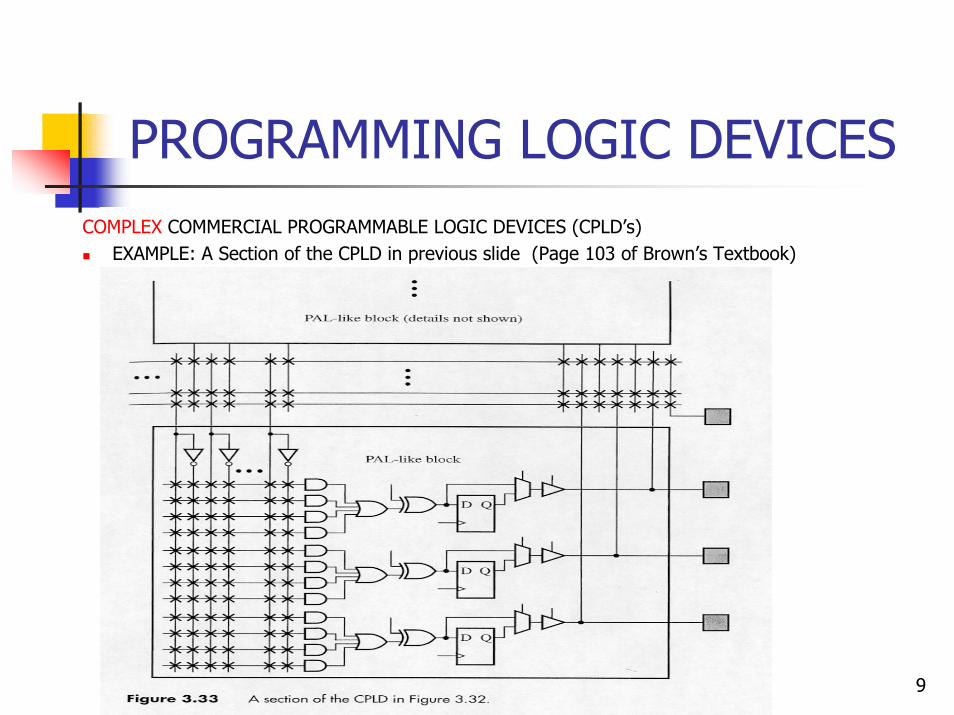
PROGRAMMING LOGIC DEVICESCOMPLEX COMMERCIAL PROGRAMMABLE LOGIC DEVICES (CPLD’s)
EXAMPLE: A Section of the CPLD in previous slide (Page 103 of Brown’s Textbook)

Copyright © 2004 by Miguel A. Marin Revised 2005-02-03 10
PROGRAMMING LOGIC DEVICES
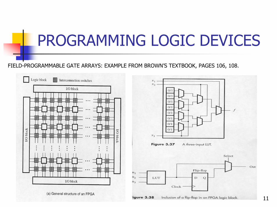
FIELD-PROGRAMMABLE GATE ARRAYS (FPGA’S)FPGA’S USE LUT’S INSTEAD OF THE AND-OR ARRAYS OF PLA’S AND PAL’S.THE LUT’S ARE CONNECTED (PROGRAMMED) THROUGH INTERCONNECTION SWITCHES.THEY HAVE EXTRA CIRCUITRY,SUCH AS STORAGE CELLS AND MUX’s, AS IN PAL’S.STORAGE CELLS ARE VOLATILE. AT POWER-ON, A PROM LOADS AUTOMATICLY THE CELLS CONTENTS.THE PROM IS HOUSED ON THE SAME CIRCUIT BOARD.
Copyright © 2004 by Miguel A. Marin Revised 2005-02-03 11
PROGRAMMING LOGIC DEVICESFIELD-PROGRAMMABLE GATE ARRAYS: EXAMPLE FROM BROWN’S TEXTBOOK, PAGES 106, 108.

12
IMPLEMENTATION EXAMPLESFPG’S: EXAMPLE CONTINUES FROM BROWN’S TEXTBOOK, PAGES 109.
NOTE: BLUE CONNECTIONS IN TEXTBOOK ARE SHOWN HERE WITH A CIRCLE
Copyright © 2004 by Miguel A. Marin Revised 2005-02-03 13
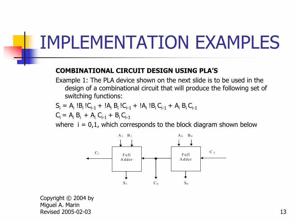
IMPLEMENTATION EXAMPLESCOMBINATIONAL CIRCUIT DESIGN USING PLA’S Example 1: The PLA device shown on the next slide is to be used in the
design of a combinational circuit that will produce the following set of switching functions:
Si = Ai !Bi !Ci-1 + !Ai Bi !Ci-1 + !Ai !Bi Ci-1 + Ai Bi Ci-1
Ci = Ai Bi + Ai Ci-1 + Bi Ci-1
where i = 0,1, which corresponds to the block diagram shown below
F u ll
A d d er
F u ll
A d d er
S 1 C 0 S 0
C -1
A 1 B 1 A 0 B 0
C 1

14
IMPLEMENTATION EXAMPLESCOMBINATIONAL CIRCUIT DESIGN USING PLA’SExample 1 (Continues): Commercial PLA device to be used in this design example

Copyright © 2004 by Miguel A. Marin Revised 2005-02-03 15
IMPLEMENTATION EXAMPLESCOMBINATIONAL CIRCUIT DESIGN USING PLA’S Example 1 (continues):
a) Give the algebraic expression of the 4 functions in such a way that they can be produced by the given PLA device.b) On the drawing of the PLA device, indicate the correct connections to produce the given 4 functions.
_________________________________________________Solution: a) The equations areS0 = A0 !B0 !C-1 + !A0 B0 !C-1 + !A0 !B0 C-1 + A0 B0 C-1
C0 = A0 B0 + A0 C-1 + B0 C-1
S1 = A1 !B1 !C0 + !A1 B1 !C0 + !A1 !B1 C0 + A1 B1 C0
C1 = A1 B1 + A1 C0 + B1 C0

Copyright © 2004 by Miguel A. Marin Revised 2005-02-03 16
IMPLEMENTATION EXAMPLESCOMBINATIONAL CIRCUIT DESIGN USING PLA’S Example 1 (continues): b) Note that the adder requires 5 inputs and that there are
only 4 dedicated input pins in the given PLA device. Bidirectional pin 5 is used as another input by conveniently programming its tri-state gate. The carry term C0 is used to compute S1 and C1 through the feedback line from pin 6, thus allowing C0 to be combined with A1 and B1 as required by the equations shown in part a).
The final circuit is shown on the next slide.

17
IMPLEMENTATION EXAMPLESCOMBINATIONAL CIRCUIT DESIGN USING PLA’S
Example (continues): Final PLA circuit

Copyright © 2004 by Miguel A. Marin Revised 2005-02-03 18
IMPLEMENTATION EXAMPLESCOMBINATIONAL CIRCUIT DESIGN USING PAL’SExample 2: On the given PAL device drawing, shown on the next
slide, indicate the correct connections that will produce the following set of equations:
F1 = !E F !D + !E F C + BF2 = !D + C + !E F BF3 = !E F B A !D

Copyright © 2004 by Miguel A. Marin Revised 2005-02-03 19
IMPLEMENTATION EXAMPLESCOMBINATIONAL CIRCUIT DESIGN USING PAL’SExample 2 (Continues) : Drawing of the PAL to be used in this example

Copyright © 2004 by Miguel A. Marin Revised 2005-02-03 20
IMPLEMENTATION EXAMPLESCOMBINATIONAL CIRCUIT DESIGN USING PAL’SExample 2 (Continues):SOLUTION:
F1 = !E F !D + !E F C + B = (!E F) (!D + C) + BF2 = !D + C + !E F B = (!D + C) + (!E F) BF3 = !E F B A !D = (!E F) B A !D
By factoring, the feedback functions (!E F) and (!D + C) were found,making the implementation feasible.
The complete circuit is shown on the next slide

Copyright © 2004 by Miguel A. Marin Revised 2005-02-03 21
IMPLEMENTATION EXAMPLESCOMBINATIONAL CIRCUIT DESIGN USING PAL’SExample 2 (Continues): Complete circuit

Copyright © 2004 by Miguel A. Marin Revised 2005-02-03 22
IMPLEMENTATION EXAMPLESCOMBINATIONAL CIRCUIT DESIGN USING MSI BUILDING BLOCKS
A block diagram is produced using the available MSI BUILDING BLOCKS and showing the behavior of the circuit to be designed.Example: Design a ONE-DIGIT Binary-Coded-Decimal (BCD)-Adder using 4-bit binary adders.
Solution: There are two cases to consider:Case I : Let the result be Z = X + Y , where X and Y are the two decimal digits to be added. If Z ≤ 9, then the binary sum S = Z and the binary carry-out = 0. If Z > 9, then Z = S + 6 and decimal carry-out = 1.Case II : When X + Y > 15 (Example: 9 + 8 =17), then the binary sum S must be corrected by adding 6 to S to produce Z = S + 6; the binary carry-out = 1 and the decimal carry-out =1.
THE BLOCK DIAGRAM IS SHOWN ON NEXT SLIDE

Copyright © 2004 by Miguel A. Marin Revised 2005-02-03 23
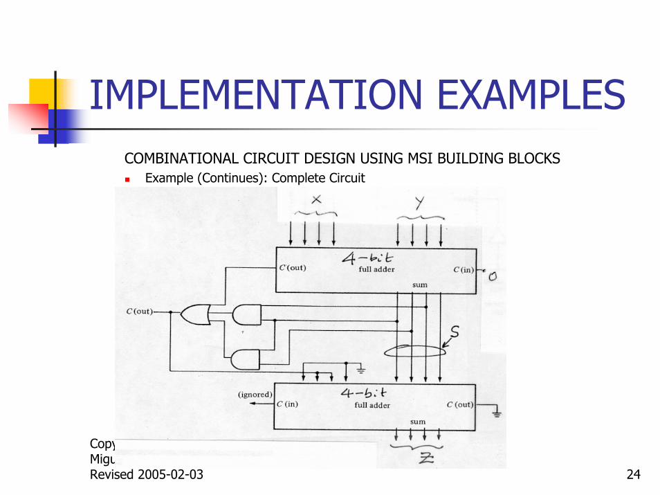
IMPLEMENTATION EXAMPLESCOMBINATIONAL CIRCUIT DESIGN USING MSI BUILDING BLOCKS
Example (Continues): Block diagram of the ONE-DIGIT BCD-adder
decimal carry-out
(ignore)
Copyright © 2004 by Miguel A. Marin Revised 2005-02-03 24
IMPLEMENTATION EXAMPLESCOMBINATIONAL CIRCUIT DESIGN USING MSI BUILDING BLOCKS
Example (Continues): Complete Circuit

Copyright © 2004 by Miguel A. Marin Revised 2005-02-03 25
IMPLEMENTATION EXAMPLESDESIGN EXAMPLE USING SEVERAL IMPLEMENTATION STRATEGIES
Design a 2-bit Binary-Coded-Base-3 Multiplier using five different implementation strategies:
Classic, two-level gate designMUX-based designROM-based designPLA-based designPAL-based design
Show on a table the gate count and packages count for each strategy.

Copyright © 2004 by Miguel A. Marin Revised 2005-02-03 26
IMPLEMENTATION EXAMPLES
1102002
0201001
0000000210
ab
C ={c3, c2, c1, c0}
Design a 2-bit Binary-Coded-Base-3 Multiplier using five different implementation strategies:
Classic, two-level gate design.Solution: The input variables are: a = {a1, a0}, b = {b1, b0}The output variables are: c = {c3, c2, c1, c0}, such that c = a x b , where x representsarithmetic multiplication.The base-3 digits, “0”, “1” and “2”arecoded 00, 01, 10 respectively. The multiplication table is

Copyright © 2004 by Miguel A. Marin Revised 2005-02-03 27
IMPLEMENTATION EXAMPLESDesign a 2-bit Binary-Coded-Base-3 Multiplier
Classic, two-level gate design continues.The K-maps of the output variables are
C3 = 0 C2 = a1b1 C1 = a1b0 + a0b1 C0 = a1b1 + a0b0
a1a0
b1 b0 00 01 11 10 0 0 0 0 * 0 0 1 0 0 * 0 1 1 * * * * 1 0 0 0 * 0
a1a0 b1 b0 00 01 11 10 0 0 0 0 * 0 0 1 0 0 * 0 1 1 * * * * 1 0 0 0 * 1
a1a0 b1 b0 00 01 11 10 0 0 0 0 * 0 0 1 0 0 * 1 1 1 * * * * 1 0 0 1 * 0
a1a0 b1 b0 00 01 11 10 0 0 0 0 * 0 0 1 0 1 * 0 1 1 * * * * 1 0 0 0 * 1

Copyright © 2004 by Miguel A. Marin Revised 2005-02-03 28
IMPLEMENTATION EXAMPLESDesign a 2-bit Binary-Coded-Base-3 Multiplier
Classic, two-level gate design continues. NAND-NAND circuit.
Copyright © 2004 by Miguel A. Marin Revised 2005-02-03 29
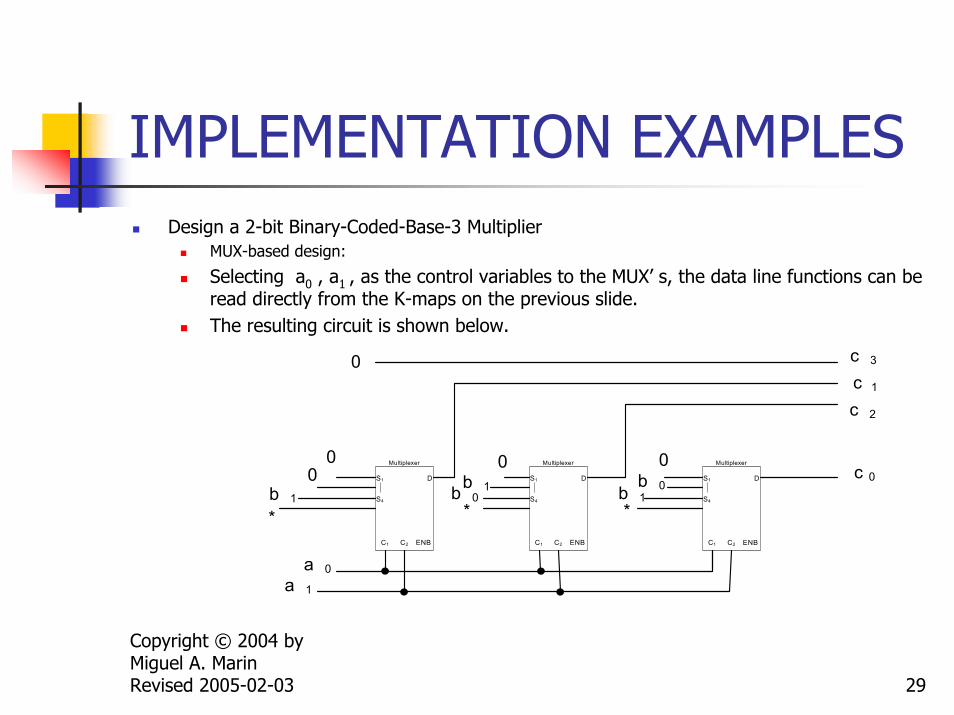
IMPLEMENTATION EXAMPLESDesign a 2-bit Binary-Coded-Base-3 Multiplier
MUX-based design:
Selecting a0 , a1 , as the control variables to the MUX’ s, the data line functions can be read directly from the K-maps on the previous slide.The resulting circuit is shown below.
S1
S4
D
C2C1 ENB
Multiplexer
S1
S4
D
C2C1 ENB
Multiplexer
S1
S4
D
C2C1 ENB
Multiplexer00
b 1*
0b 1b 0*
b 1b 0
*
a 0a 1
0 c 3
c 1c 2
c 00

Copyright © 2004 by Miguel A. Marin Revised 2005-02-03 30
IMPLEMENTATION EXAMPLESDesign a 2-bit Binary-Coded-Base-3 Multiplier
ROM-based designThe address of the ROM represents the valuation of the input variables and the contents, at that address, corresponds to the value of the output variables for that valuation of the input variables.An address/contents table is produced and the ROM is programmed accordingly.
B A S E - 3 D I G I T S
A D D R E S S
C O N T E N T S
b a b 1 b 0 a 1 a 0 c 3 c 2 c 1 c 0 0 0 0 0 0 0 0 0 0 0 0 1 0 0 0 1 0 0 0 0 0 2 0 0 1 0 0 0 0 0 0 * 0 0 1 1 * * * * 1 0 0 1 0 0 0 0 0 0 1 1 0 1 0 1 0 0 0 1 1 2 0 1 1 0 0 0 1 0 1 * 0 1 1 1 * * * * 2 0 1 0 0 0 0 0 0 0 2 1 1 0 0 1 0 0 1 0 2 2 1 0 1 0 0 1 0 1 2 * 1 0 1 1 * * * * * 0 1 1 0 0 0 0 0 0 * 1 1 1 0 1 * * * * * 2 1 1 1 0 * * * * * * 1 1 1 1 * * * *

Copyright © 2004 by Miguel A. Marin Revised 2005-02-03 31
IMPLEMENTATION EXAMPLESDesign a 2-bit Binary-Coded-Base-3 Multiplier
ROM-based design: Final circuit
16 words 3-bits per
word ROM
DATA REGISTER
c3 c2 c1 c0
AD
DR
ESS
DEC
OD
ER a0
a1
b0
b1

Copyright © 2004 by Miguel A. Marin Revised 2005-02-03 32
IMPLEMENTATION EXAMPLESDesign a 2-bit Binary-Coded-Base-3 Multiplier
PLA-based design: Note that the term a1 b1 can be shared among output functions c0 and c2 .
b 1 b 0 a 1 a 0
c 3 c 2 c 1 c 0
0

Copyright © 2004 by Miguel A. Marin Revised 2005-02-03 33
IMPLEMENTATION EXAMPLESDesign a 2-bit Binary-Coded-Base-3 Multiplier
PAL-based design: Note that NO SHARING of terms is allowed in PAL-based design and, therefore, term a1 b1 must be implemented twice b 1 b 0 a 1 a 0
c 3 c 2 c 1 c 0
0

Copyright © 2004 by Miguel A. Marin Revised 2005-02-03 34
IMPLEMENTATION EXAMPLESDesign a 2-bit Binary-Coded-Base-3 MultiplierIMPLEMENTATION STATEGIES COMPARISON:
In order to compare the different strategies used in this design we choose the following metrics:
1) The number of gate-equivalences and 2) The number of packages.
We assume that the 7400 Series is used for the classic, two-level NAND-NAND design. For example: the 7400 IC package, called QUAD, contains 4 2-input NAND gates).The number of gates used in a 4 x 1 MUX is equal to 7 (cf. Brown’s Textbook, 2nd Ed. Page 317). One package houses 2 MUX’s.Finally we assume that in the ROM-based design, the decoder requires 19 gates, 16 for each minterm and 3 gates for the output level.The following table shows the results.

Copyright © 2004 by Miguel A. Marin Revised 2005-02-03 35
IMPLEMENTATION EXAMPLESDesign a 2-bit Binary-Coded-Base-3 Multiplier
IMPLEMENTATION STATEGIES COMPARISON RESULTS
The design using the least number of packages and the least number of gates is the PLA-based design.
81PAL
71PLA
191ROM
212MUX
72Gate
Total number of gate equivalences
Number of Packages
Design Approach