Embed Size (px)
Citation preview

Department of Electrical and Computer Engineering ECSE-330B Electronic Circuits I
MOSFETs 1
Biasing in MOSFET Amplifiers
• Biasing: Creating the circuit to establish the desired DC voltages and currents for the operation of the amplifier
• Four common ways:1. Biasing by fixing VGS
2. Biasing by fixing VG and connecting a resistance in the Source
3. Biasing using a Drain-to-Gate Feedback Resistor4. Biasing Using a Constant-Current Source
Department of Electrical and Computer Engineering ECSE-330B Electronic Circuits I
MOSFETs 2
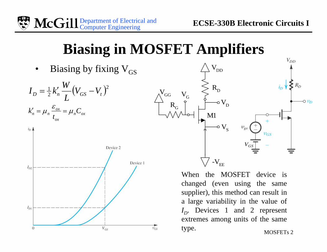
Biasing in MOSFET Amplifiers• Biasing by fixing VGS
When the MOSFET device is changed (even using the same supplier), this method can result in a large variability in the value of ID. Devices 1 and 2 represent extremes among units of the same type.
( )221
tGSnD VVL
WkI −′=
oxnox
oxnn C
tk μεμ ==′
VDD
-VEE
VGG
RG
RD
RS
M1
VGVD
VS

Department of Electrical and Computer Engineering ECSE-330B Electronic Circuits I
MOSFETs 3
Biasing in MOSFET Amplifiers• Biasing by fixing VG and connecting a resistance in the Source
Degeneration Resistance

Department of Electrical and Computer Engineering ECSE-330B Electronic Circuits I
MOSFETs 4
Biasing in MOSFET Amplifiers• Biasing using a Drain-to-Gate Feedback Resistor
Large Resistor

Department of Electrical and Computer Engineering ECSE-330B Electronic Circuits I
MOSFETs 5
Biasing in MOSFET Amplifiers• Biasing Using a Constant-Current Source
Figure 4.33 (a) Biasing the MOSFET using a constant-current source I. (b) Implementation of the constant-current source Iusing a current mirror.
Current Mirror
Used in Integrated Circuits

Department of Electrical and Computer Engineering ECSE-330B Electronic Circuits I
MOSFETs 6
Current Mirror DC Analysis• The width and length (the W/L aspect
ratio) and the parameters of the two transistors can be different
• We can choose W/L freely• In this circuit, consider W/L of both
MOSFETs are the same and transistors are identical. The Gate-Source voltages are also the same, then
( )21
121
tGSnREF VVLWkI −′=
( )21
121
tGSn VVLWkI −′=
REF
REF
IIWL
LW
II
=
=⋅= 11
1
1
1
W1
L1
VGS VGS
+
--
+
W1
L1
I
Department of Electrical and Computer Engineering ECSE-330B Electronic Circuits I
MOSFETs 7
Current Mirror DC Analysis
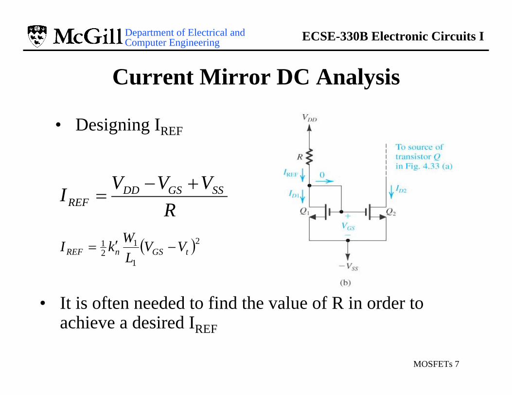
• Designing IREF
RVVVI SSGSDD
REF+−
=
( )21
121
tGSnREF VVLWkI −′=
• It is often needed to find the value of R in order to achieve a desired IREF

Department of Electrical and Computer Engineering ECSE-330B Electronic Circuits I
MOSFETs 8
Biasing of MOSFET Amplifier
• 1- Intro to MOS Field Effect Transistor (MOSFET)• 2- NMOS FET• 3- PMOS FET• 4- DC Analysis of MOSFET Circuits• 5- MOSFET Amplifier• 6- MOSFET Small Signal Model• 7- MOSFET Integrated Circuits• 8- CSA, CGA, CDA• 9- CMOS Inverter & MOS Digital Logic

Department of Electrical and Computer Engineering ECSE-330B Electronic Circuits I
MOSFETs 9
MOSFET Design Space• Modern integrated circuits use MOSFETs
extensively– Very high densities of transistors – up to 109
transistors/cm2 in some ULSI memory arrays.– Off-chip discrete resistors and capacitors are NOT
commonly used– On-chip resistors and capacitors generally small– Multistage amplifiers are usually DC-coupled
• Transistors used wherever possible to implement current sources, resistors, capacitors,

Department of Electrical and Computer Engineering ECSE-330B Electronic Circuits I
MOSFETs 10
Using MOSFETs to implement R’s and C’s
• Resistors:Active Loads (large R’s)Diode-connected loads (small R’s)MOSFET Triode-Region (moderate R’s)
• CapacitorsMost obvious is the gate-body capacitorCan be used to have variable-capacitors as well
• Current Mirrors
Department of Electrical and Computer Engineering ECSE-330B Electronic Circuits I
MOSFETs 11
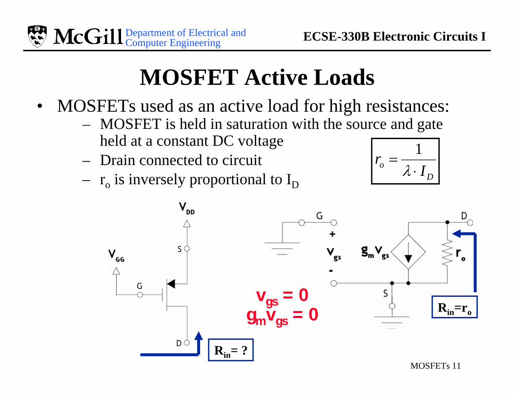
MOSFET Active Loads• MOSFETs used as an active load for high resistances:
– MOSFET is held in saturation with the source and gate held at a constant DC voltage
– Drain connected to circuit
vgs = 0gmvgs = 0
Do I
r⋅
=λ
1
– ro is inversely proportional to ID
Rin= ?
Rin=ro

Department of Electrical and Computer Engineering ECSE-330B Electronic Circuits I
MOSFETs 12
Diode-Connected MOSFETs• A Diode connected MOSFET can be used to achieve
small resistances:– The Drain is directly connected to Gate, and therefore it
can only be operated in saturation (or cutoff)
Source Absorption Theorem
Department of Electrical and Computer Engineering ECSE-330B Electronic Circuits I
MOSFETs 13
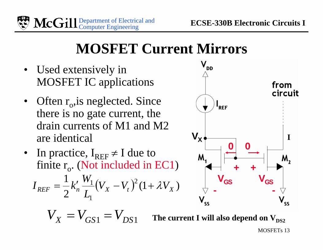
MOSFET Current Mirrors• Used extensively in
MOSFET IC applications
• Often ro,is neglected. Since there is no gate current, the drain currents of M1 and M2 are identical
• In practice, IREF ≠ I due to finite ro. (Not included in EC1)
VGS VGS
+
--
+
0 0
( ) )1(21 2
1
1XtXnREF VVV
LWkI λ+−′=
11 DSGSX VVV ==
VX
The current I will also depend on VDS2
I

Department of Electrical and Computer Engineering ECSE-330B Electronic Circuits I
MOSFETs 14
Current Mirror DC Analysis• The width and length (the W/L
aspect ratio) of MOSFETs can be designed almost freely
• Since the W/L of M1 and M2need not be the same, the size ratios can affect current ratios
( )21
121
tGSnREF VVLWkI −′=
( )22
221
tGSn VVLWkI −′=
1
1
2
2
WL
LW
II
REF⋅=
W1
L1
W2
L2
VGS VGS
+
--
+
I
Department of Electrical and Computer Engineering ECSE-330B Electronic Circuits I
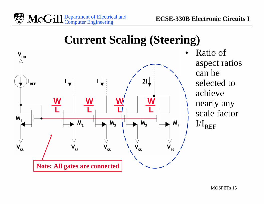
MOSFETs 15
Current Scaling (Steering)• Ratio of
aspect ratios can be selected to achieve nearly any scale factor I/IREF
WL
WL
WL
WL
Note: All gates are connected
Department of Electrical and Computer Engineering ECSE-330B Electronic Circuits I
MOSFETs 16
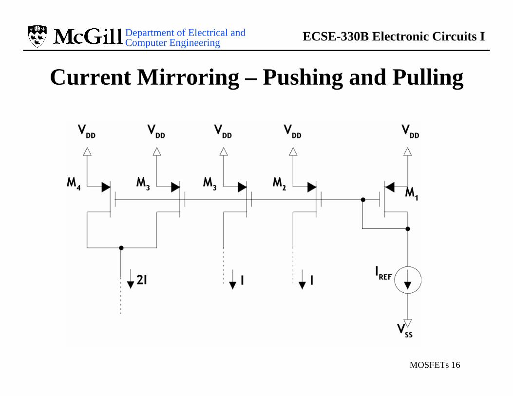
Current Mirroring – Pushing and Pulling
Department of Electrical and Computer Engineering ECSE-330B Electronic Circuits I
MOSFETs 17
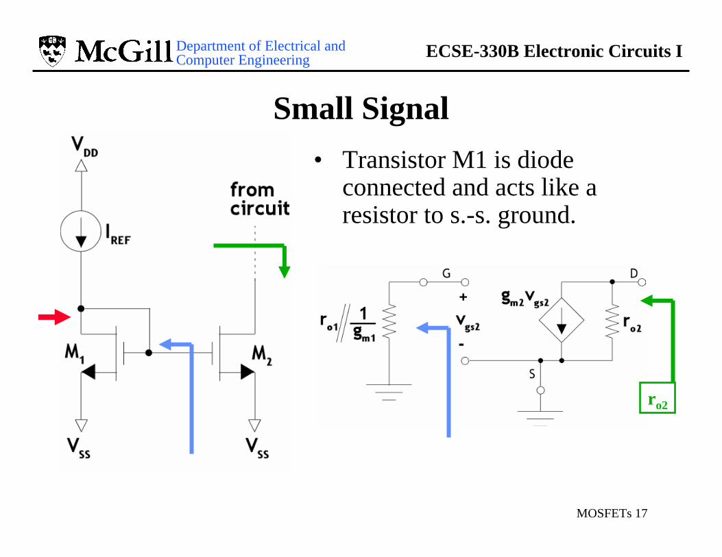
Small Signal• Transistor M1 is diode
connected and acts like a resistor to s.-s. ground.
ro2
Department of Electrical and Computer Engineering ECSE-330B Electronic Circuits I
MOSFETs 18
Outline of Chapter 5
• 1- Intro to MOS Field Effect Transistor (MOSFET)• 2- NMOS FET• 3- PMOS FET• 4- DC Analysis of MOSFET Circuits• 5- MOSFET Amplifier• 6- MOSFET Small Signal Model• 7- MOSFET Integrated Circuits• 8- CSA, CGA, CDA• 9- CMOS Inverter & MOS Digital Logic

Department of Electrical and Computer Engineering ECSE-330B Electronic Circuits I
MOSFETs 19
DC and AC - Body-Effect / CLM
Three types of analysis:Neglect AC Body-Effect & AC CLM
/ Neglect AC CLMUse AC Body-Effect
Use AC Body-Effect / Use CLM
Three types of analysis:Neglect DC Body-Effect & DC CLM
/ Neglect DC CLMUse DC Body-Effect
Use DC Body-Effect / Use DC CLM
DC Analysis
AC Analysis(small-signal)
Use whatever DC values for V and I in the small-signal
analysis

Department of Electrical and Computer Engineering ECSE-330B Electronic Circuits I
MOSFETs 20
Common Source Amplifier (CSA)• Current source I implemented
with current mirror.• Current mirror provides
active load at drain• Source terminal grounded –
no DC or AC Body effect

Department of Electrical and Computer Engineering ECSE-330B Electronic Circuits I
MOSFETs 21
CSA with Current Mirror
CSA
ro2

Department of Electrical and Computer Engineering ECSE-330B Electronic Circuits I
MOSFETs 22
CSA Small Signal Analysis• From MOSFET
Current-Mirror: only ro2 appears in analysis
igs vv =1
( ) 1211 gsoomout vrrgv −=
( )211 oomi
outV rrg
vvA −==
Department of Electrical and Computer Engineering ECSE-330B Electronic Circuits I
MOSFETs 23
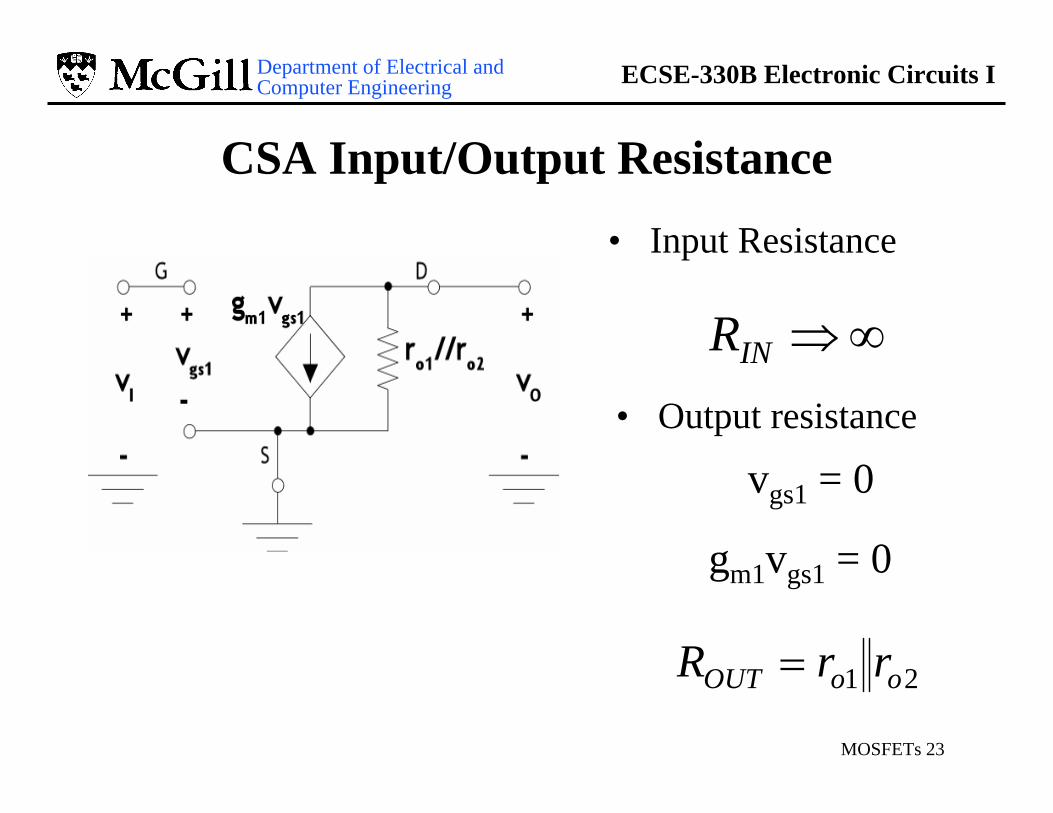
CSA Input/Output Resistance
• Input Resistance
• Output resistance
21 ooOUT rrR =
vgs1 = 0
gm1vgs1 = 0
∞⇒INR

Department of Electrical and Computer Engineering ECSE-330B Electronic Circuits I
MOSFETs 24
CSA Calculations• In practice, difficult to keep all
transistors operating in saturation VOUT is hard to control, and
sensitive to: W/L, VG, and CLM
Ω=−==
==
=′
=′
==
== −
kRVVVV
LW
LWk
kVVV
V
REF
SSDD
VA
n
VA
p
tt
12,5
40,50
125
501
01.0
1
1
2
2
21
121
μ
μ
λλ
VV
V
o
VA
m
OUT
G
Akr
mgVV
mAIVV
10052.38192.5855.3
596.2567.2
1
−=Ω=
==
==Hand: SPICE:
VV
V
OUT
G
AVV
mAIVV
4.102895.2
57.258.2
−==
==

Department of Electrical and Computer Engineering ECSE-330B Electronic Circuits I
MOSFETs 25
Common Gate Amplifier (CGA)• A pMOS current mirror is used
as IREF including the output resistance.
• Since source terminal not at signal ground, the body effect is present.
• The gate terminal held at a DC voltage. (AC Ground)
Typically used as second stage of a multi-stage amplifier circuit
Department of Electrical and Computer Engineering ECSE-330B Electronic Circuits I
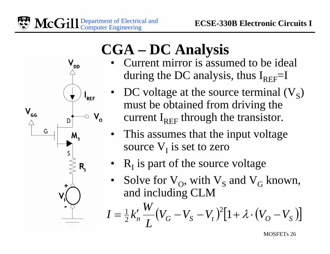
MOSFETs 26
CGA – DC Analysis• Current mirror is assumed to be ideal
during the DC analysis, thus IREF=I• DC voltage at the source terminal (VS)
must be obtained from driving the current IREF through the transistor.
• This assumes that the input voltage source VI is set to zero
• RI is part of the source voltage• Solve for VO, with VS and VG known,
and including CLM
( ) ( )[ ]SOtSGn VVVVVL
WkI −⋅+−−′= λ1221
Department of Electrical and Computer Engineering ECSE-330B Electronic Circuits I
MOSFETs 27
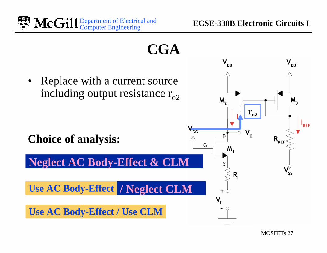
CGA
• Replace with a current source including output resistance ro2
Choice of analysis:
Neglect AC Body-Effect & CLM
/ Neglect CLMUse AC Body-Effect
Use AC Body-Effect / Use CLM
ro2

Department of Electrical and Computer Engineering ECSE-330B Electronic Circuits I
MOSFETs 28
CGA – No Body Effect or CLM
2ogsmo rvgv ⋅−=
I
Im
mgs v
Rg
gv+
−=
1
11
1
Im
o
I
oV
Rg
rvvA
+== 1
2
i=0
Non Inverting

Department of Electrical and Computer Engineering ECSE-330B Electronic Circuits I
MOSFETs 29
CGA – RIN & ROUT, No Body Effect or CLM
1
1
mIN g
R =
RIN
ROUT
2oOUT rR =
vI = 0
Department of Electrical and Computer Engineering ECSE-330B Electronic Circuits I
MOSFETs 30
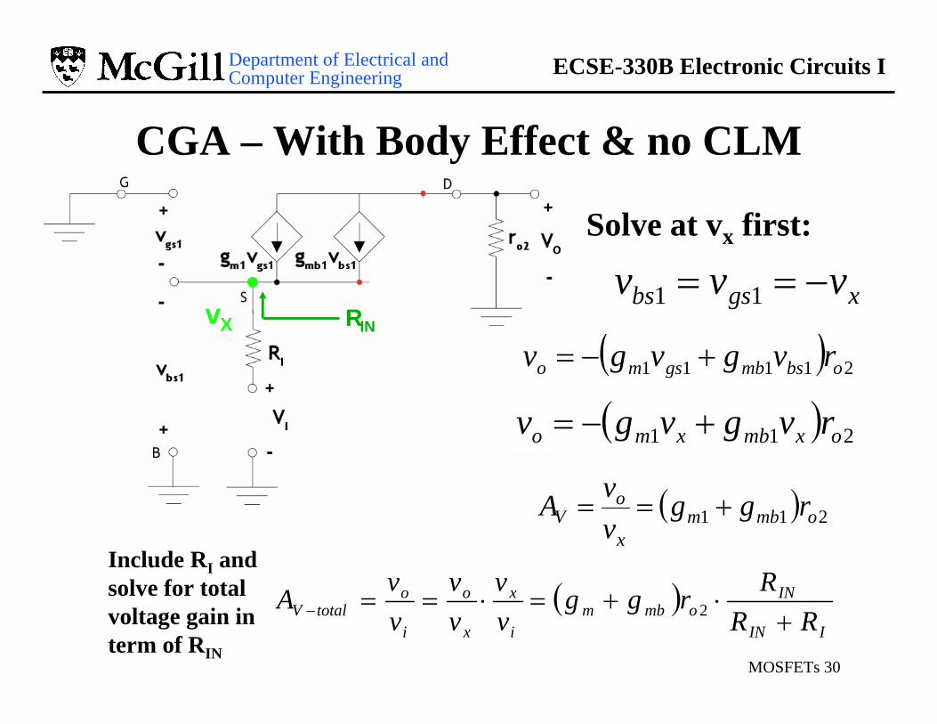
CGA – With Body Effect & no CLM
( ) 211 oxmbxmo rvgvgv +−=
( ) 211 ombmx
oV rgg
vvA +==
xgsbs vvv −== 11
( ) 21111 obsmbgsmo rvgvgv +−=
( )IIN
INombm
i
x
x
o
i
ototalV RR
Rrggvv
vv
vvA
+⋅+=⋅==− 2
Include RI and solve for total voltage gain in term of RIN
RIN
Solve at vx first:
vX

Department of Electrical and Computer Engineering ECSE-330B Electronic Circuits I
MOSFETs 31
CGA – RIN With Body Effect & no CLM
xmbmx vggi )( 11 +=
xgsbs vvv −== 11
11
1
mbmIN gg
R+
=
RINiIN
vX
Neglect InputVoltage Source
xmbmin vggi )( 11 +=
iX

Department of Electrical and Computer Engineering ECSE-330B Electronic Circuits I
MOSFETs 32
CGA - With Body Effect & CLM
Neglect InputVoltage Source
gsx vv −=
2oxo riv ⋅=
( )1
11o
oxxmbmx r
vvvggi −++=
vXiX
iX
( ) ⎟⎟⎠
⎞⎜⎜⎝
⎛++⋅== 11
121
1mbm
ooo
x
oV gg
rrr
vvA

Department of Electrical and Computer Engineering ECSE-330B Electronic Circuits I
MOSFETs 33
CGA – RIN With Body Effect & CLM
Neglect Input Voltage Source
2oxo riv ⋅=
( )1
11o
oxxmbmx r
vvvggi −++=
111
1
2
1
1
mbmo
o
o
x
xIN
ggr
rr
ivR
++
+==
RIN
iX
vX