Embed Size (px)
Citation preview
Department of Electrical and Computer Engineering ECSE-330B Electronic Circuits I
BJTs 1
Chapter 5Bipolar Junction Transistors (BJTs)
Sedra/Smith, Sections 5.1-5.9
Department of Electrical and Computer Engineering ECSE-330B Electronic Circuits I
BJTs 2
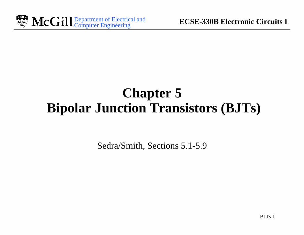
Outline of Chapter 5• 1- Introduction to The Bipolar Junction Transistor• 2- Active Mode Operation of BJT• 3- DC Analysis of Active Mode BJT Circuits• 4- BJT as an Amplifier• 5- BJT Small Signal Models• 6- CEA, CEA with RE, CBA, & CCA • 7- Integrated Circuit Amplifiers
Department of Electrical and Computer Engineering ECSE-330B Electronic Circuits I
BJTs 3
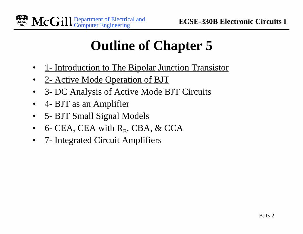
Transistors
• A three terminal device is required to implement current switches and amplifiers.– need voltage control terminal– used to control current flow through
other two terminals
• All four ideal amplifier configurations (section 1) employ dependent sources.
• A small Control “voltage” can allow a large change in “current”.
Department of Electrical and Computer Engineering ECSE-330B Electronic Circuits I
BJTs 4
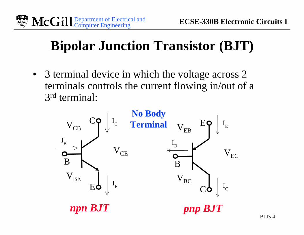
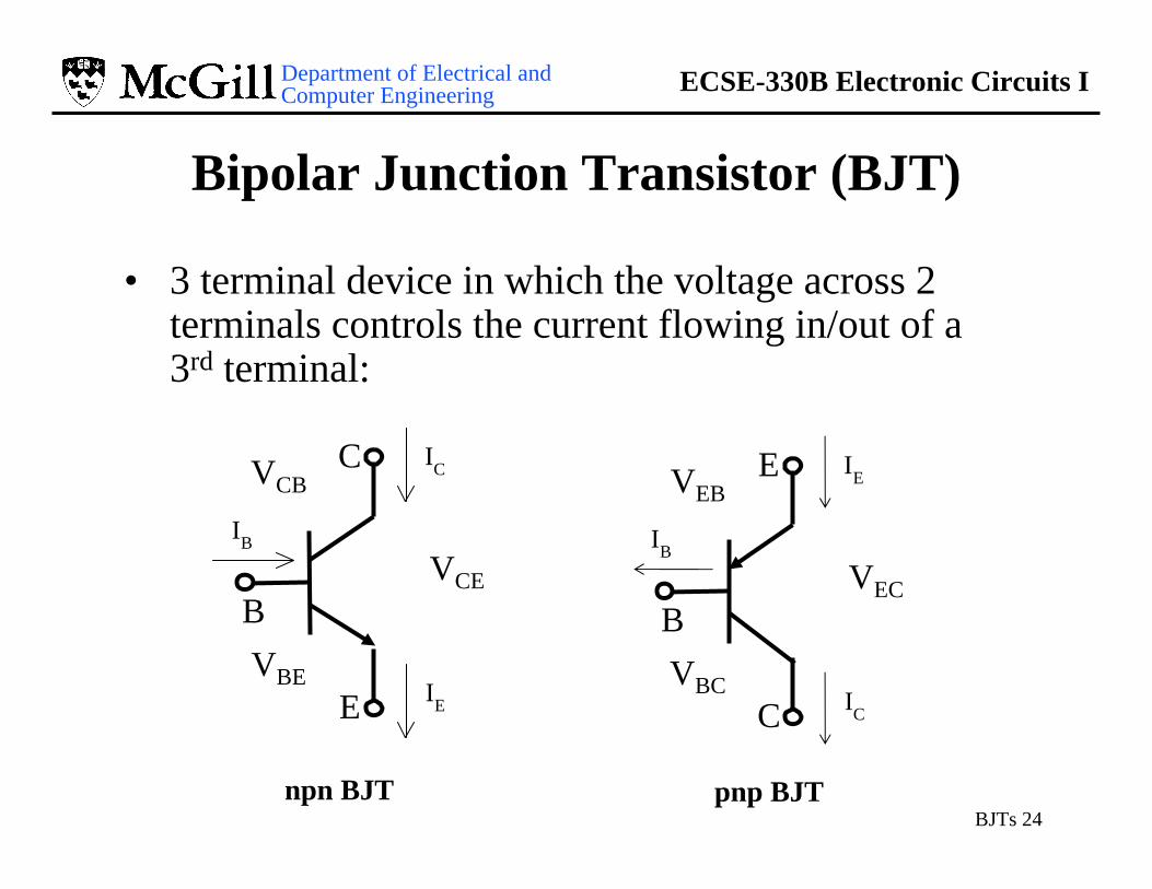
• 3 terminal device in which the voltage across 2 terminals controls the current flowing in/out of a 3rd terminal:
Bipolar Junction Transistor (BJT)
ICC
IB
B
IEEVBE
VCB
VCE
npn BJT
IEE
IB
B
ICCVBC
VEB
VEC
pnp BJT
No Body Terminal
Department of Electrical and Computer Engineering ECSE-330B Electronic Circuits I
BJTs 5
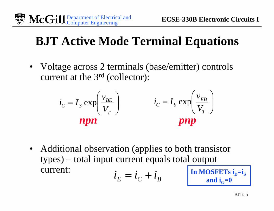
BJT Active Mode Terminal Equations
• Voltage across 2 terminals (base/emitter) controls current at the 3rd (collector):
npn pnp
• Additional observation (applies to both transistor types) – total input current equals total output current:
⎟⎟⎠
⎞⎜⎜⎝
⎛=
T
BESC V
vIi exp ⎟⎟⎠
⎞⎜⎜⎝
⎛=
T
EBSC V
vIi exp
BCE iii += In MOSFETs iD=iSand iG=0
Department of Electrical and Computer Engineering ECSE-330B Electronic Circuits I
BJTs 6
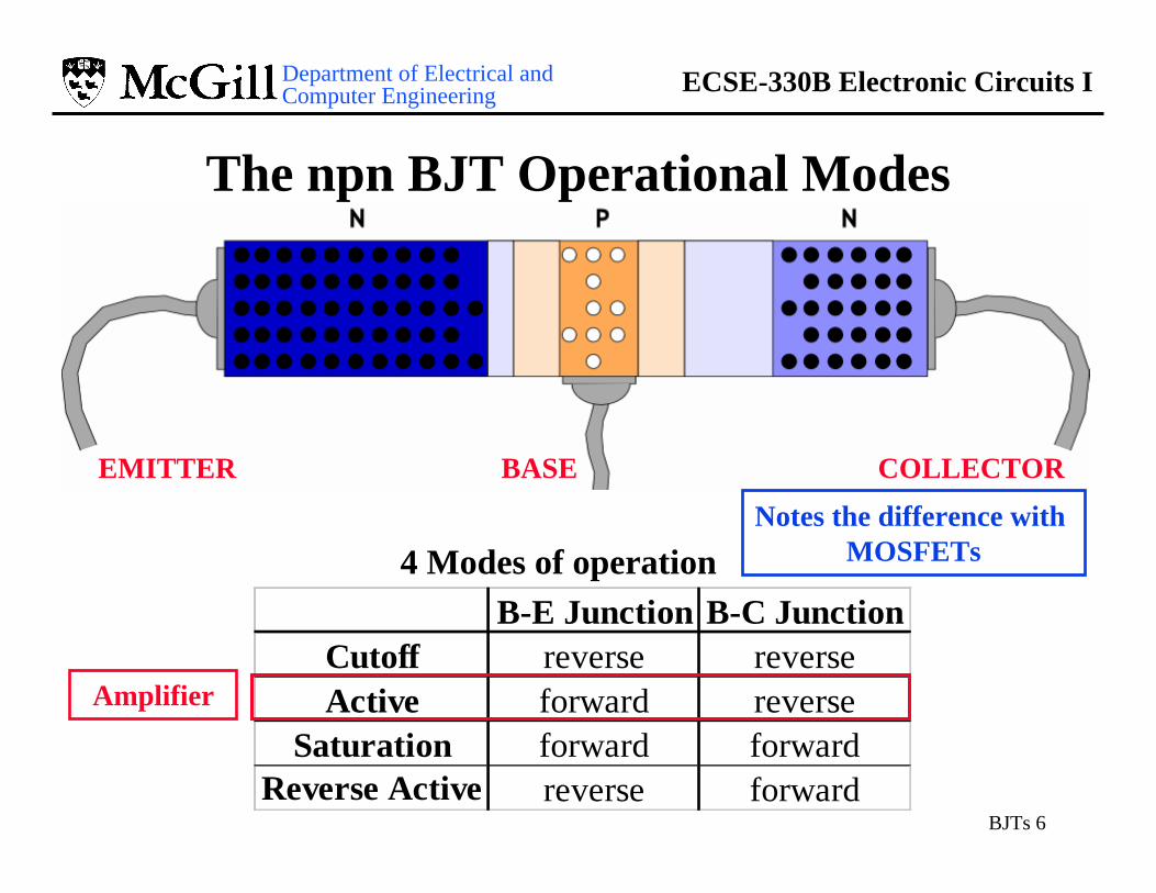
The npn BJT Operational Modes
B-E Junction B-C JunctionCutoff reverse reverseActive forward reverse
Saturation forward forwardReverse Active reverse forward
4 Modes of operation
EMITTER BASE COLLECTOR
Notes the difference with MOSFETs
Amplifier
Department of Electrical and Computer Engineering ECSE-330B Electronic Circuits I
BJTs 7
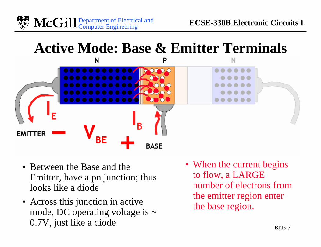
Active Mode: Base & Emitter Terminals
• Between the Base and the Emitter, have a pn junction; thus looks like a diode
• Across this junction in active mode, DC operating voltage is ~ 0.7V, just like a diode
• When the current begins to flow, a LARGE number of electrons from the emitter region enter the base region.
Department of Electrical and Computer Engineering ECSE-330B Electronic Circuits I
BJTs 8
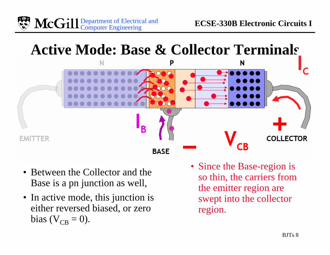
Active Mode: Base & Collector Terminals
• Between the Collector and the Base is a pn junction as well,
• In active mode, this junction is either reversed biased, or zero bias (VCB = 0).
• Since the Base-region is so thin, the carriers from the emitter region are swept into the collector region.
Department of Electrical and Computer Engineering ECSE-330B Electronic Circuits I
BJTs 9
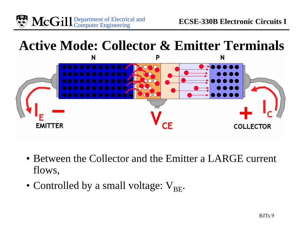
Active Mode: Collector & Emitter Terminals
• Between the Collector and the Emitter a LARGE current flows,
• Controlled by a small voltage: VBE.
Department of Electrical and Computer Engineering ECSE-330B Electronic Circuits I
BJTs 10
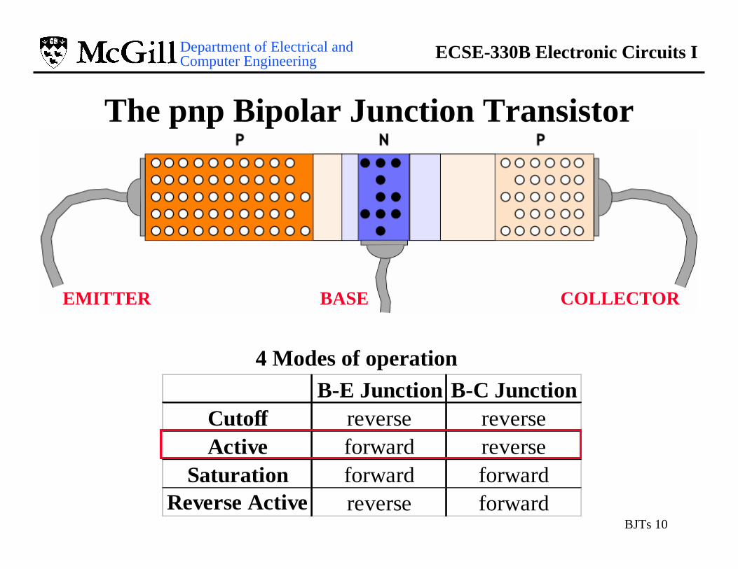
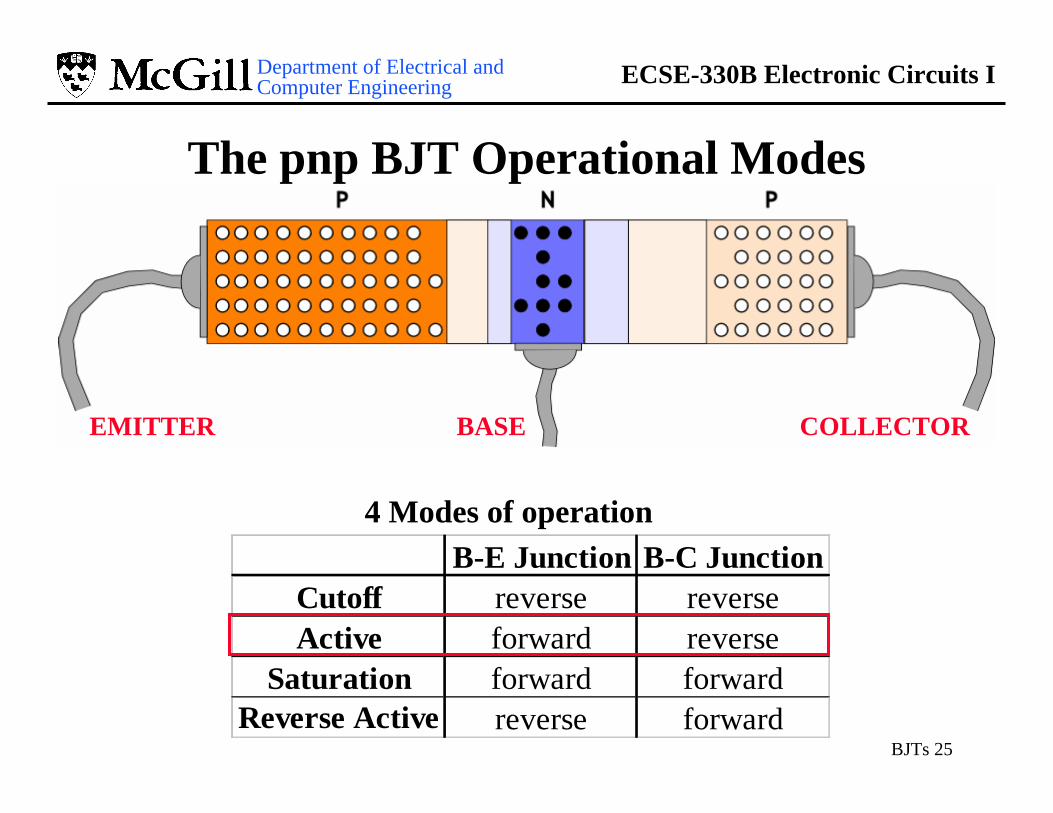
The pnp Bipolar Junction Transistor
EMITTER BASE COLLECTOR
B-E Junction B-C JunctionCutoff reverse reverseActive forward reverse
Saturation forward forwardReverse Active reverse forward
4 Modes of operation
Department of Electrical and Computer Engineering ECSE-330B Electronic Circuits I
BJTs 11
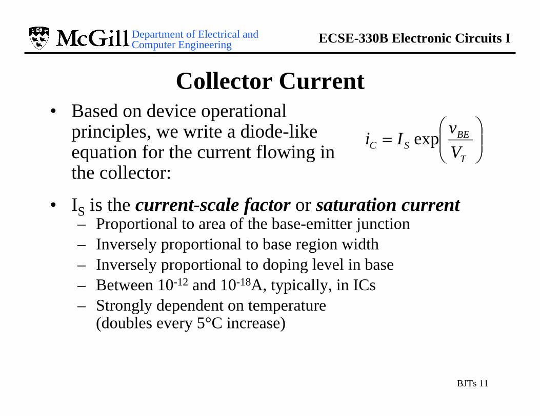
Collector Current• Based on device operational
principles, we write a diode-like equation for the current flowing in the collector:
⎟⎟⎠
⎞⎜⎜⎝
⎛=
T
BESC V
vIi exp
• IS is the current-scale factor or saturation current– Proportional to area of the base-emitter junction– Inversely proportional to base region width– Inversely proportional to doping level in base– Between 10-12 and 10-18A, typically, in ICs– Strongly dependent on temperature
(doubles every 5°C increase)
Department of Electrical and Computer Engineering ECSE-330B Electronic Circuits I
BJTs 12
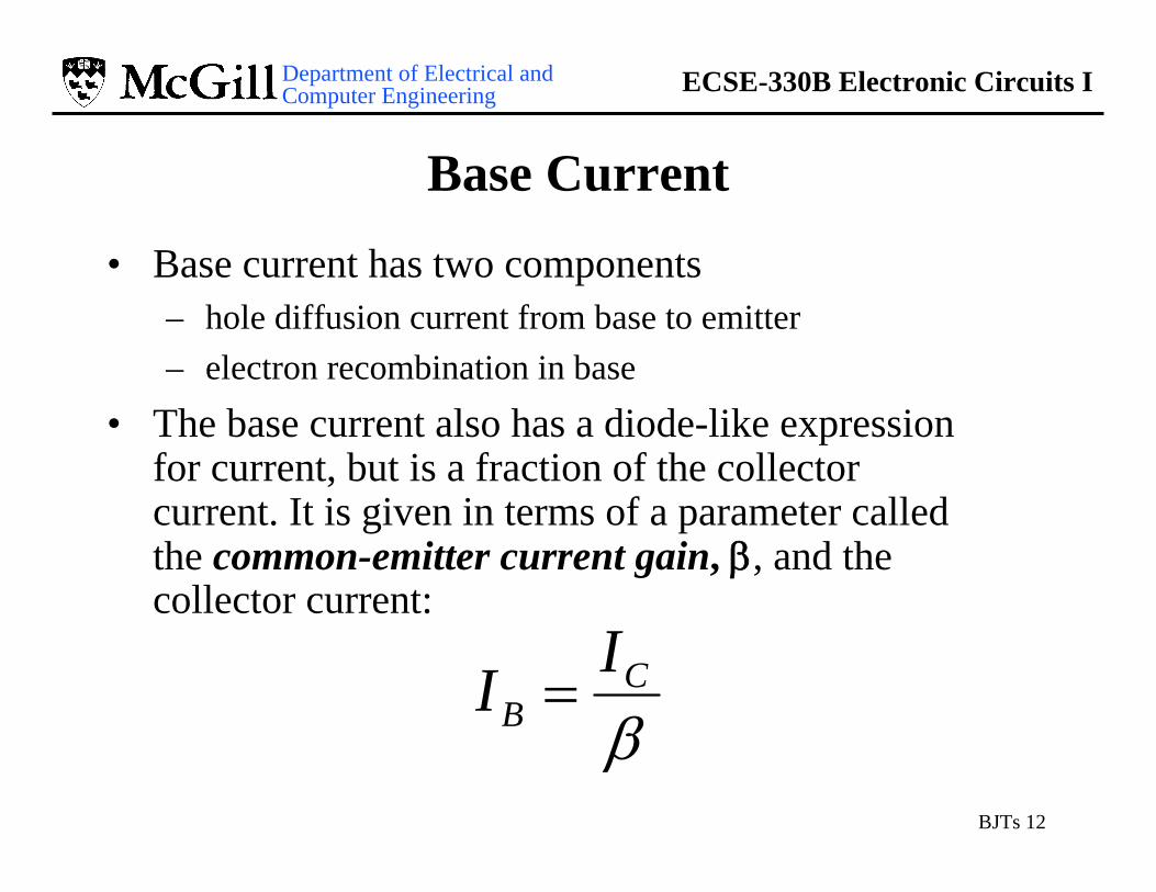
Base Current
• Base current has two components– hole diffusion current from base to emitter– electron recombination in base
• The base current also has a diode-like expression for current, but is a fraction of the collector current. It is given in terms of a parameter called the common-emitter current gain, β, and the collector current:
βC
BII =
Department of Electrical and Computer Engineering ECSE-330B Electronic Circuits I
BJTs 13
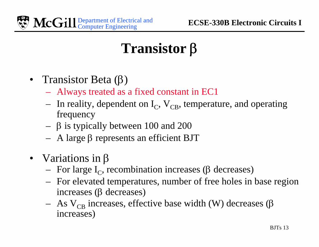
Transistor β
• Transistor Beta (β)– Always treated as a fixed constant in EC1– In reality, dependent on IC, VCB, temperature, and operating
frequency
– For large IC, recombination increases (β decreases)
– β is typically between 100 and 200– A large β represents an efficient BJT
• Variations in β
– For elevated temperatures, number of free holes in base region increases (β decreases)
– As VCB increases, effective base width (W) decreases (βincreases)
Department of Electrical and Computer Engineering ECSE-330B Electronic Circuits I
BJTs 14
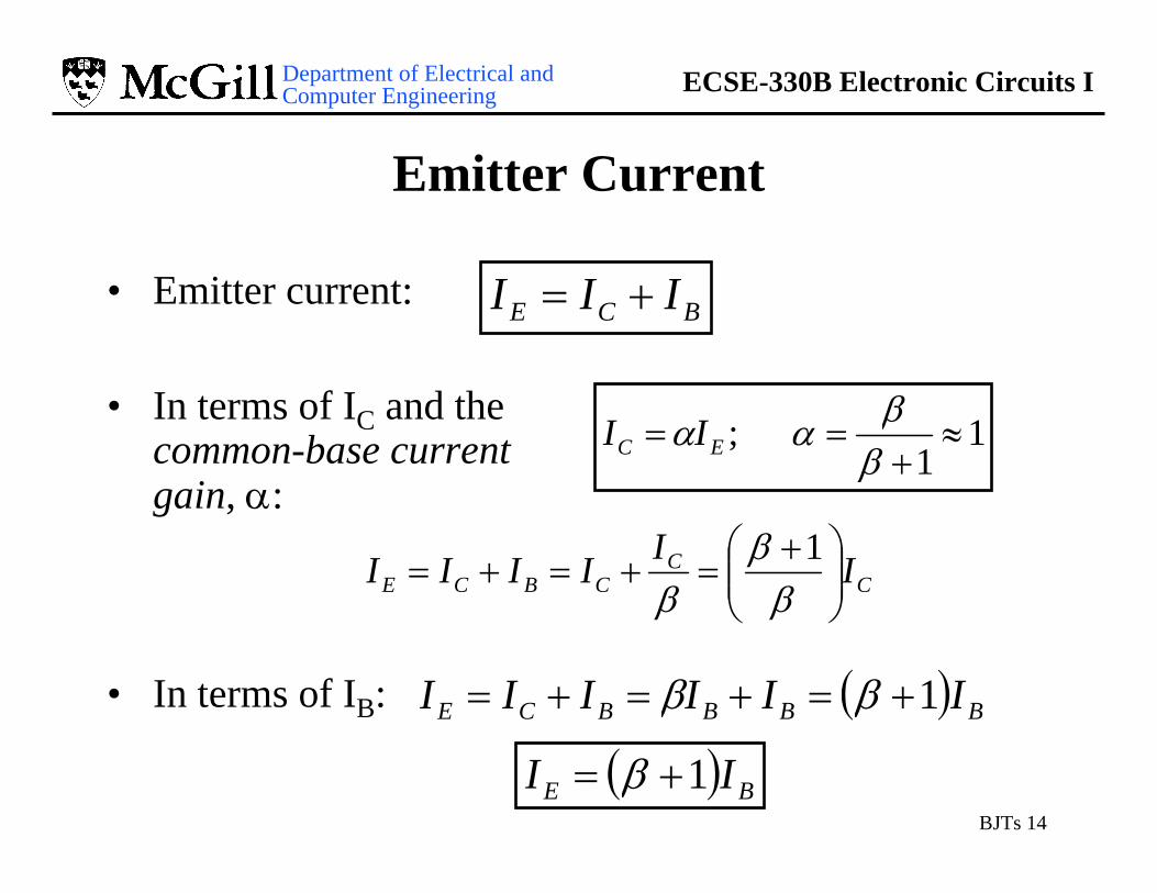
Emitter Current
• Emitter current: BCE III +=
• In terms of IC and the common-base current gain, α:
CC
CBCE IIIIII ⎟⎟⎠
⎞⎜⎜⎝
⎛ +=+=+=
ββ
β1
11
; ≈+
==ββαα EC II
• In terms of IB: ( ) BBBBCE IIIIII 1+=+=+= ββ
( ) BE II 1+= β
Department of Electrical and Computer Engineering ECSE-330B Electronic Circuits I
BJTs 15
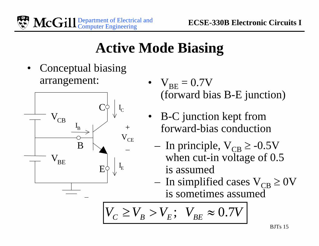
Active Mode Biasing• Conceptual biasing
arrangement: • VBE = 0.7V (forward bias B-E junction)
• B-C junction kept from forward-bias conduction
VVVVV BEEBC 7.0 ; ≈>≥
– In principle, VCB ≥ -0.5V when cut-in voltage of 0.5 is assumed
– In simplified cases VCB ≥ 0V is sometimes assumed
ICC
IB
B
IEE
VCB
VBE
+VCE
_
Department of Electrical and Computer Engineering ECSE-330B Electronic Circuits I
BJTs 16
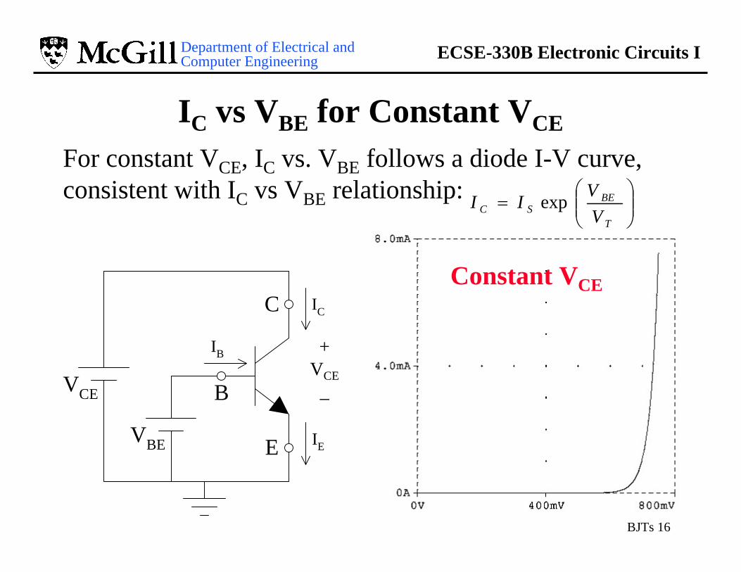
IC vs VBE for Constant VCE
ICC
IB
B
IEE
VCE
VBE
Constant VCE
+VCE
_
For constant VCE, IC vs. VBE follows a diode I-V curve, consistent with IC vs VBE relationship:
⎟⎟⎠
⎞⎜⎜⎝
⎛=
T
BESC V
VII exp
Department of Electrical and Computer Engineering ECSE-330B Electronic Circuits I
BJTs 17
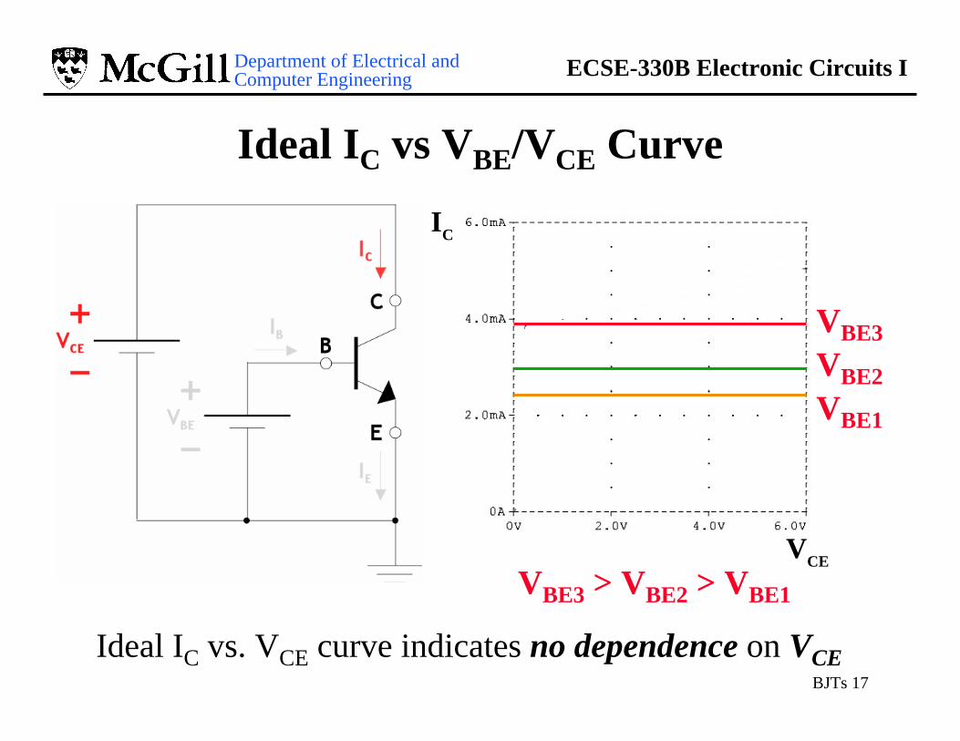
Ideal IC vs VBE/VCE Curve
VCE
IC
VBE1
Ideal IC vs. VCE curve indicates no dependence on VCE
VBE2
VBE3
VBE3 > VBE2 > VBE1
Department of Electrical and Computer Engineering ECSE-330B Electronic Circuits I
BJTs 18
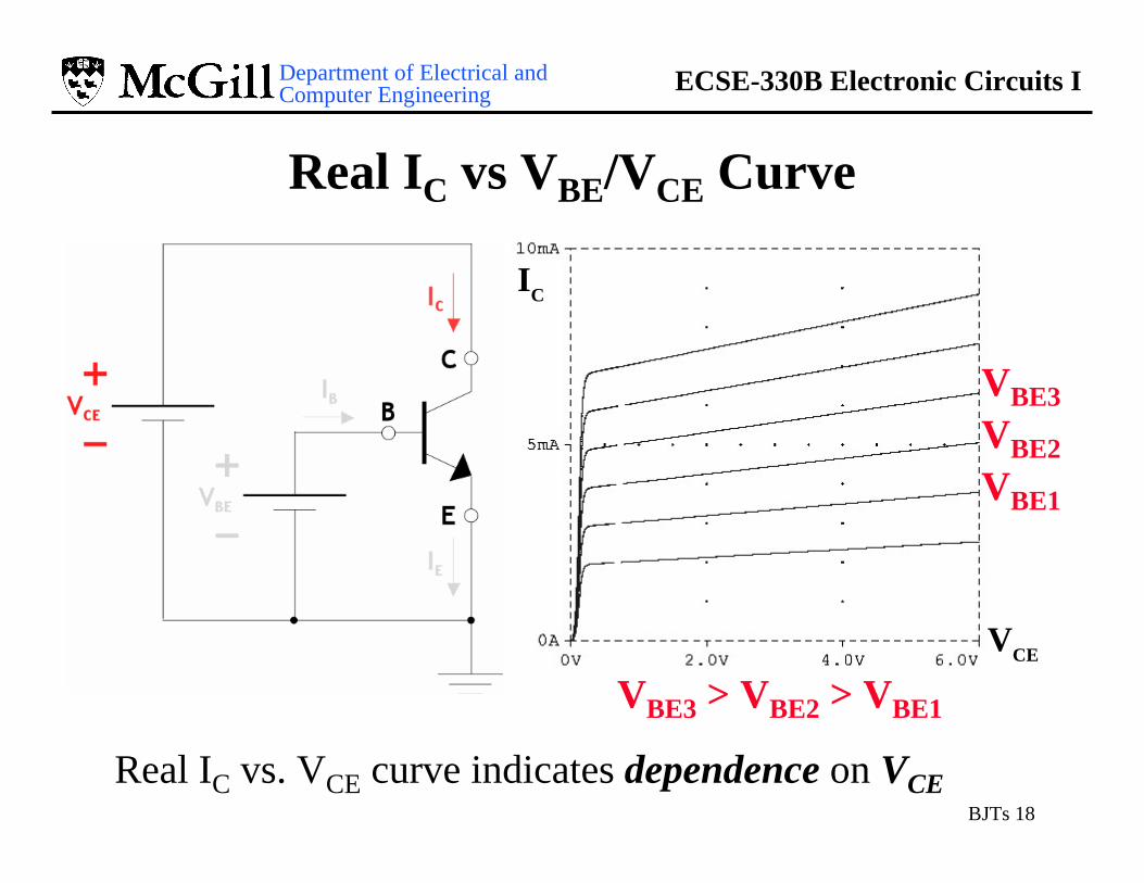
Real IC vs VBE/VCE Curve
VBE1
Real IC vs. VCE curve indicates dependence on VCE
VBE2
VBE3
VBE3 > VBE2 > VBE1
VCE
IC
Department of Electrical and Computer Engineering ECSE-330B Electronic Circuits I
BJTs 19
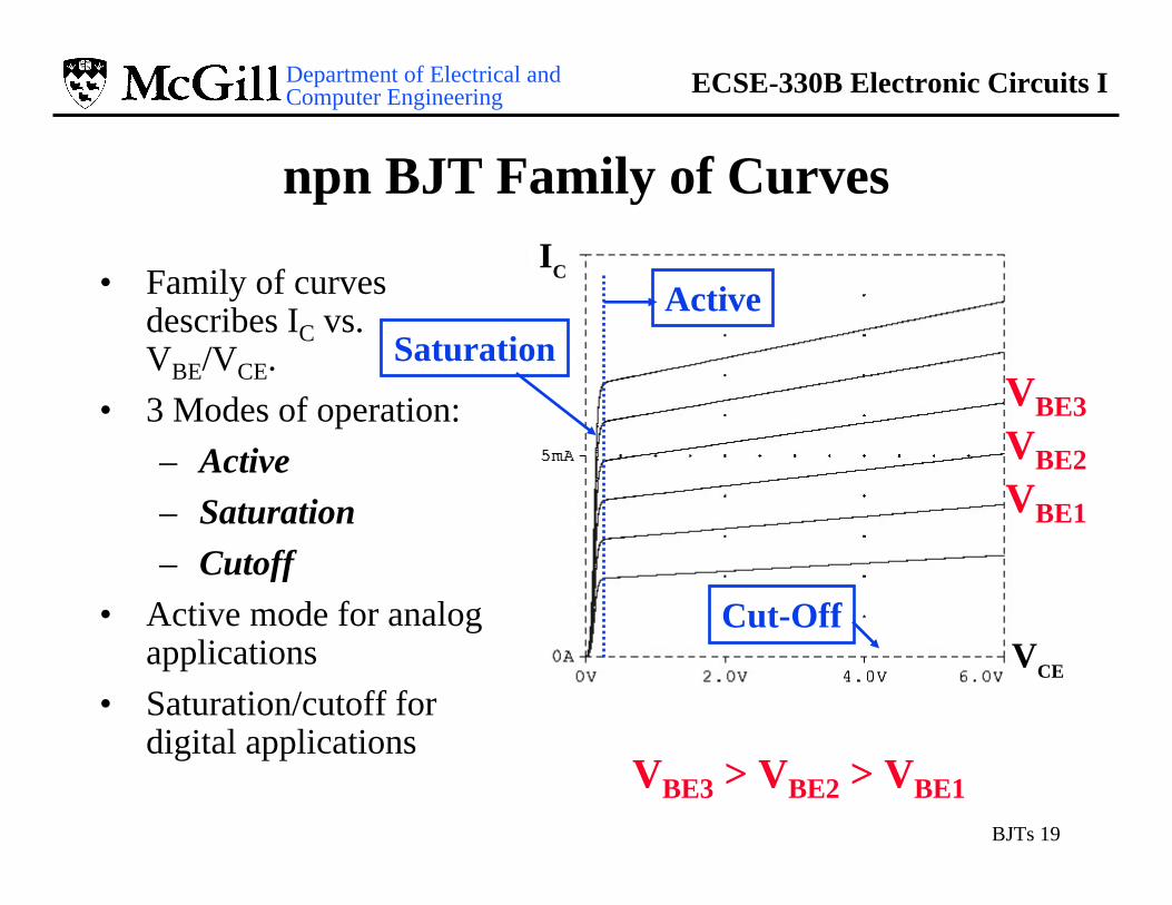
npn BJT Family of Curves
• Family of curves describes IC vs. VBE/VCE.
• 3 Modes of operation:– Active– Saturation– Cutoff
• Active mode for analog applications
• Saturation/cutoff for digital applications
VBE1
VBE2
VBE3
VBE3 > VBE2 > VBE1
VCE
IC
ActiveSaturation
Cut-Off
Department of Electrical and Computer Engineering ECSE-330B Electronic Circuits I
BJTs 20
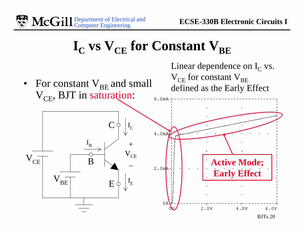
IC vs VCE for Constant VBE
• For constant VBE and small VCE, BJT in saturation:
ICC
IB
B
IEE
VCE
VBE
+VCE
_
Linear dependence on IC vs. VCE for constant VBEdefined as the Early Effect
Active Mode; Early Effect
Department of Electrical and Computer Engineering ECSE-330B Electronic Circuits I
BJTs 21
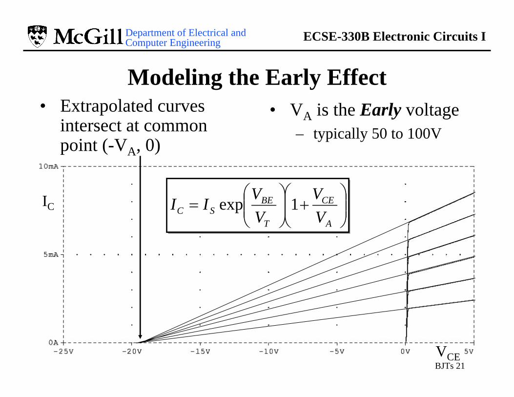
Modeling the Early Effect• Extrapolated curves
intersect at common point (-VA, 0)
• VA is the Early voltage– typically 50 to 100V
⎟⎟⎠
⎞⎜⎜⎝
⎛+⎟⎟
⎠
⎞⎜⎜⎝
⎛=
A
CE
T
BESC V
VVVII 1expIC
VCE
Department of Electrical and Computer Engineering ECSE-330B Electronic Circuits I
BJTs 22
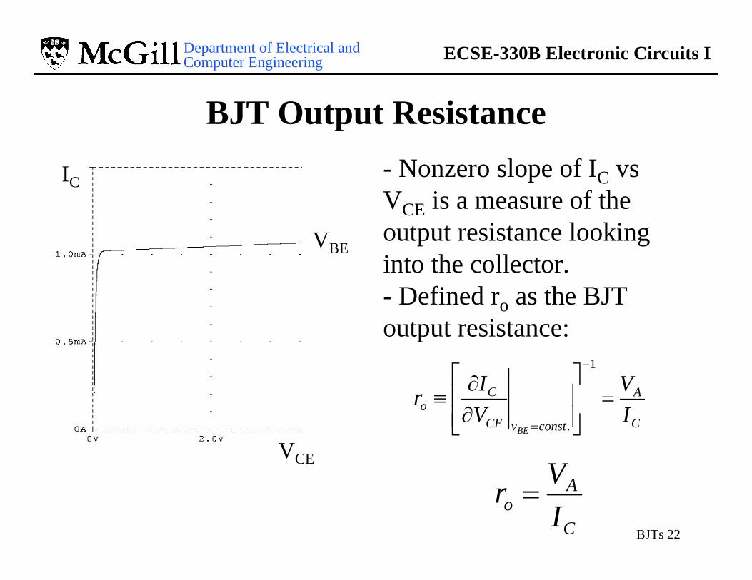
BJT Output Resistance
C
A
constvCE
Co I
VVIr
BE
=⎥⎥⎦
⎤
⎢⎢⎣
⎡
∂∂
≡
−
=
1
.
- Nonzero slope of IC vsVCE is a measure of the output resistance looking into the collector.- Defined ro as the BJT output resistance:
IC
VCE
VBE
C
Ao I
Vr =
Department of Electrical and Computer Engineering ECSE-330B Electronic Circuits I
BJTs 23
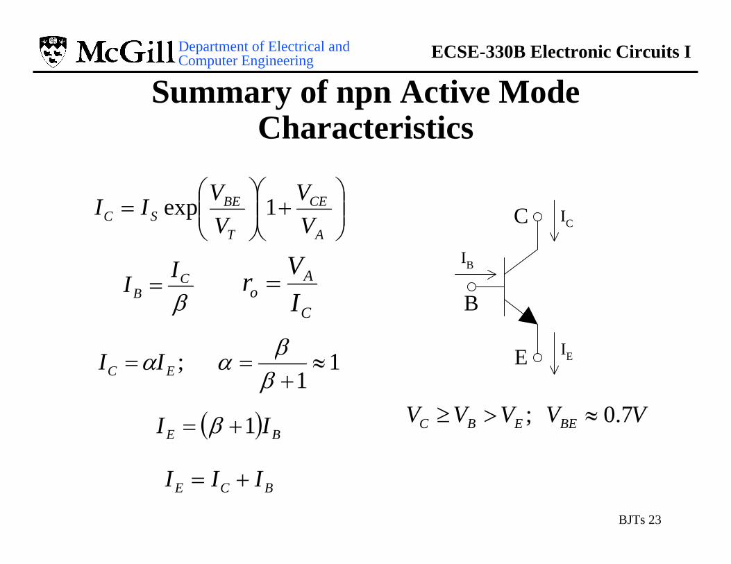
Summary of npn Active Mode Characteristics
⎟⎟⎠
⎞⎜⎜⎝
⎛+⎟⎟
⎠
⎞⎜⎜⎝
⎛=
A
CE
T
BESC V
VVVII 1exp
βC
BII =
( ) BE II 1+= β VVVVV BEEBC 7.0 ; ≈>≥
ICC
IB
B
IEE11
; ≈+
==ββαα EC II
BCE III +=
C
Ao I
Vr =
Department of Electrical and Computer Engineering ECSE-330B Electronic Circuits I
BJTs 24
• 3 terminal device in which the voltage across 2 terminals controls the current flowing in/out of a 3rd terminal:
Bipolar Junction Transistor (BJT)
ICC
IB
B
IEEVBE
VCB
VCE
npn BJT
IEE
IB
B
ICCVBC
VEB
VEC
pnp BJT
Department of Electrical and Computer Engineering ECSE-330B Electronic Circuits I
BJTs 25
The pnp BJT Operational Modes
EMITTER BASE COLLECTOR
B-E Junction B-C JunctionCutoff reverse reverseActive forward reverse
Saturation forward forwardReverse Active reverse forward
4 Modes of operation
Department of Electrical and Computer Engineering ECSE-330B Electronic Circuits I
BJTs 26
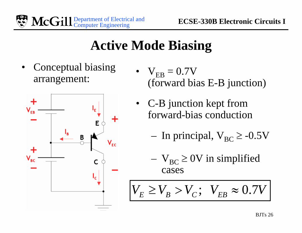
Active Mode Biasing
• VEB = 0.7V (forward bias E-B junction)
• C-B junction kept from forward-bias conduction
VVVVV EBCBE 7.0 ; ≈>≥
– In principal, VBC ≥ -0.5V
– VBC ≥ 0V in simplified cases
• Conceptual biasing arrangement:

Department of Electrical and Computer Engineering ECSE-330B Electronic Circuits I
BJTs 27
Summary of pnp Active Mode Characteristics
⎟⎟⎠
⎞⎜⎜⎝
⎛+⎟⎟
⎠
⎞⎜⎜⎝
⎛=
A
EC
T
EBSC V
VVVII 1exp
VVVVV EBCBE 7.0 ; ≈>≥
IEE
IB
B
ICCβC
BII =
( ) BE II 1+= β
11
; ≈+
==ββαα EC II
BCE III +=
pnp
C
Ao I
Vr =
Department of Electrical and Computer Engineering ECSE-330B Electronic Circuits I
BJTs 28
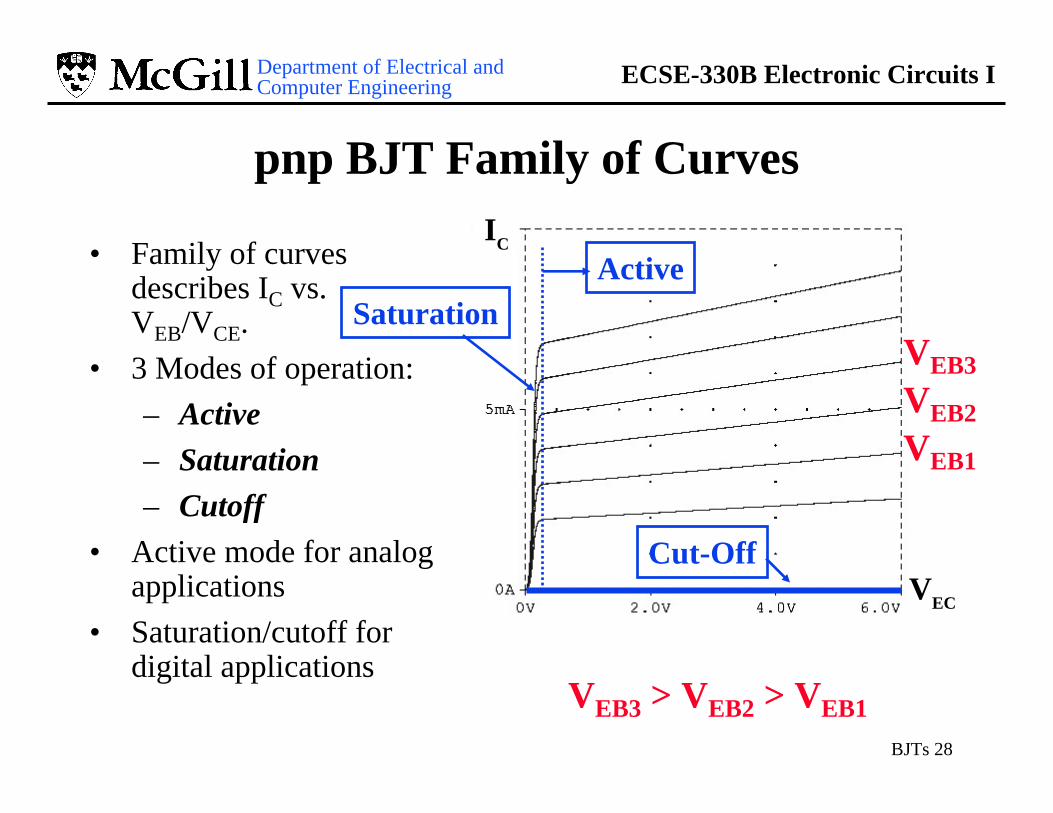
pnp BJT Family of Curves
• Family of curves describes IC vs. VEB/VCE.
• 3 Modes of operation:– Active– Saturation– Cutoff
• Active mode for analog applications
• Saturation/cutoff for digital applications
VEB1
VEB2
VEB3
VEB3 > VEB2 > VEB1
VEC
IC
ActiveSaturation
Cut-Off


![Chapter 4 Introduction to Bipolar Junction Transistors (BJTs)...Introduction to Bipolar Junction Transistors (BJTs) 4.1 Introduction [5] The transistor was invented by a team of three](https://img.dokumen.tips/doc/110x75/5f73167be644cf1b4d346cf2/chapter-4-introduction-to-bipolar-junction-transistors-bjts-introduction-to.jpg)