Embed Size (px)
Citation preview
Introduction to
CMOS VLSI
Design
Delay Calculations
CMOS VLSI Design
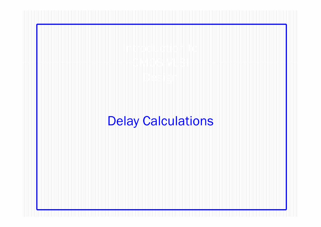
Transient Response
MOS equations
� DC analysis tells us Vout if Vin is constant
� Transient analysis tells us Vout(t) if Vin(t) changes� Requires solving differential equations
� Input is usually considered to be a step or ramp� From 0 to VDD or vice versa
CMOS VLSI Design
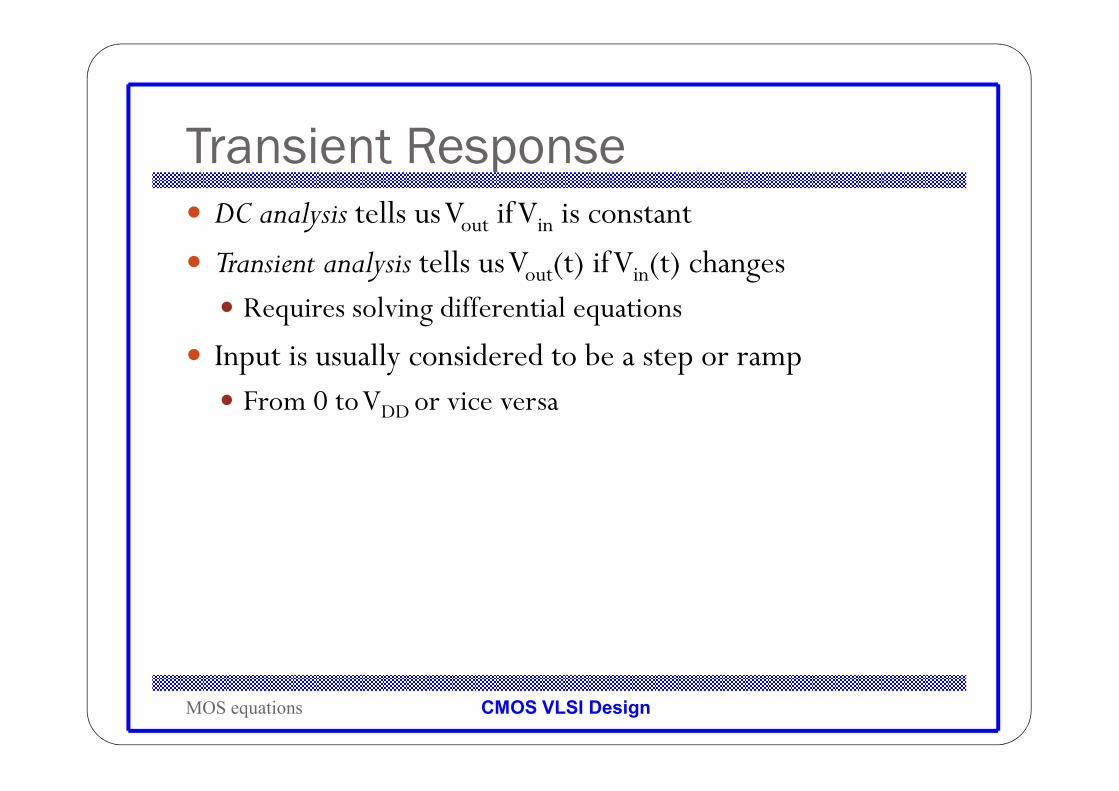
Simulated Inverter Delay
MOS equations
� Solving differential equations by hand is too hard
� SPICE simulator solves the equations numerically� Uses more accurate I-V models too!
� But simulations take time to write
(V)
0.0
0.5
1.0
1.5
2.0
t(s)0.0 200p 400p 600p 800p 1n
tpdf = 66ps t
pdr = 83psV
inVout
CMOS VLSI Design
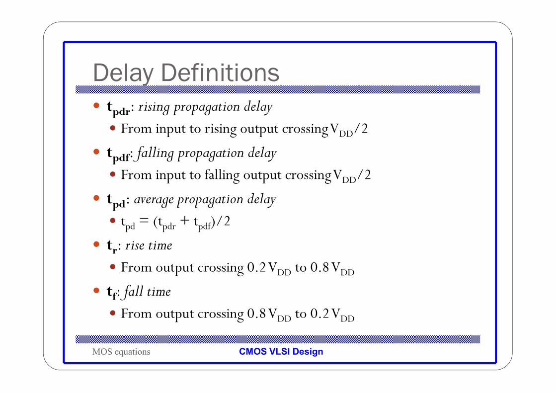
Delay Definitions
MOS equations
� tpdr: rising propagation delay� From input to rising output crossing VDD/2
� tpdf: falling propagation delay� From input to falling output crossing VDD/2
� tpd: average propagation delay� tpd = (tpdr + tpdf)/2
� tr: rise time� From output crossing 0.2 VDD to 0.8 VDD
� tf: fall time� From output crossing 0.8 VDD to 0.2 VDD
CMOS VLSI Design
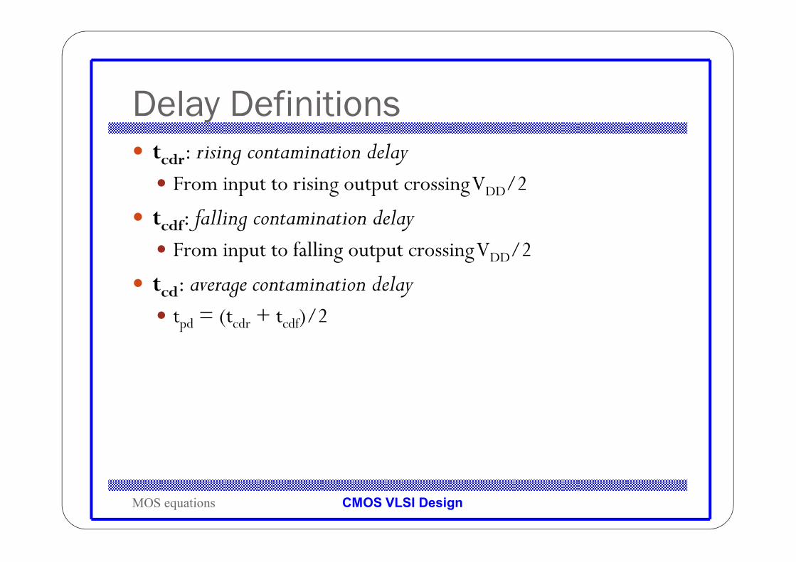
Delay Definitions
MOS equations
� tcdr: rising contamination delay� From input to rising output crossing VDD/2
� tcdf: falling contamination delay� From input to falling output crossing VDD/2
� tcd: average contamination delay� tpd = (tcdr + tcdf)/2
CMOS VLSI Design
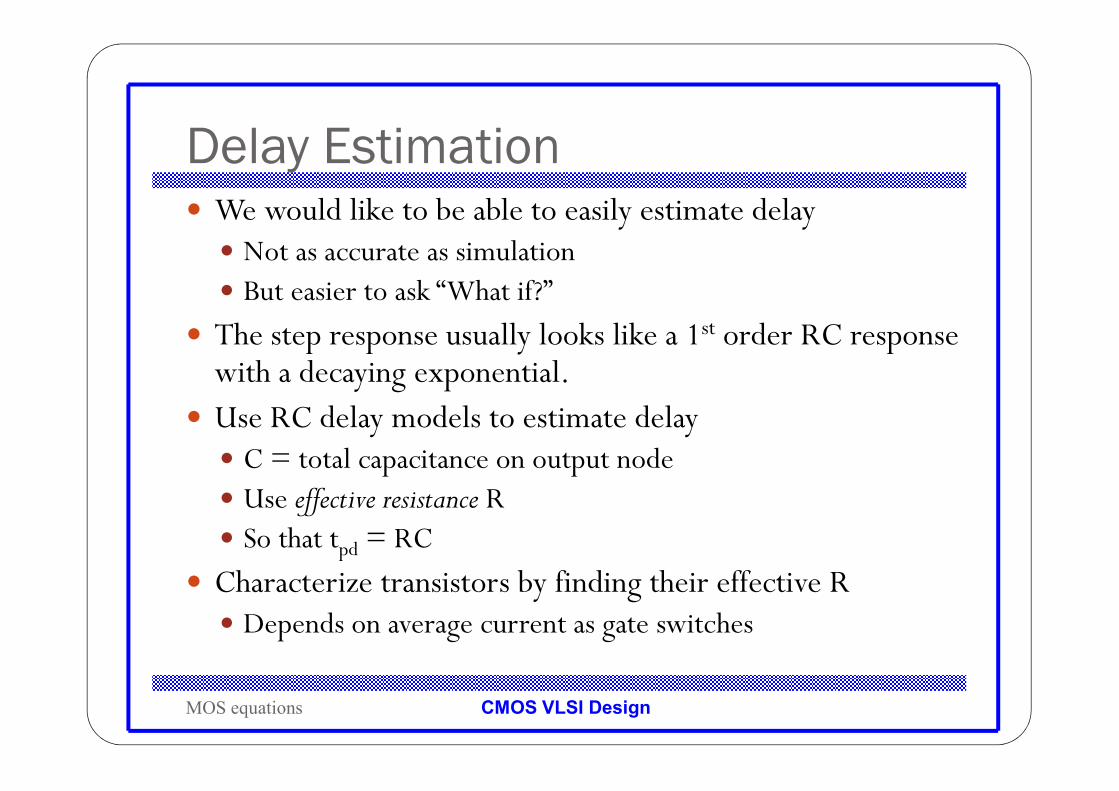
Delay Estimation
MOS equations
� We would like to be able to easily estimate delay� Not as accurate as simulation� But easier to ask “What if?”
� The step response usually looks like a 1st order RC response with a decaying exponential.
� Use RC delay models to estimate delay� C = total capacitance on output node� Use effective resistance R� So that tpd = RC
� Characterize transistors by finding their effective R� Depends on average current as gate switches
CMOS VLSI Design
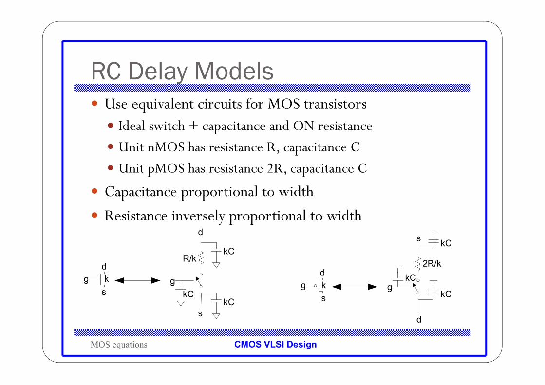
RC Delay Models
MOS equations
� Use equivalent circuits for MOS transistors� Ideal switch + capacitance and ON resistance
� Unit nMOS has resistance R, capacitance C
� Unit pMOS has resistance 2R, capacitance C
� Capacitance proportional to width
� Resistance inversely proportional to width
kg
s
d
g
s
d
kCkC
kCR/k
kg
s
d
g
s
d
kC
kC
kC
2R/k
CMOS VLSI Design
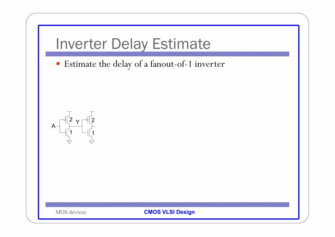
Inverter Delay Estimate
MOS devices
� Estimate the delay of a fanout-of-1 inverter
2
1A
Y 2
1
CMOS VLSI Design
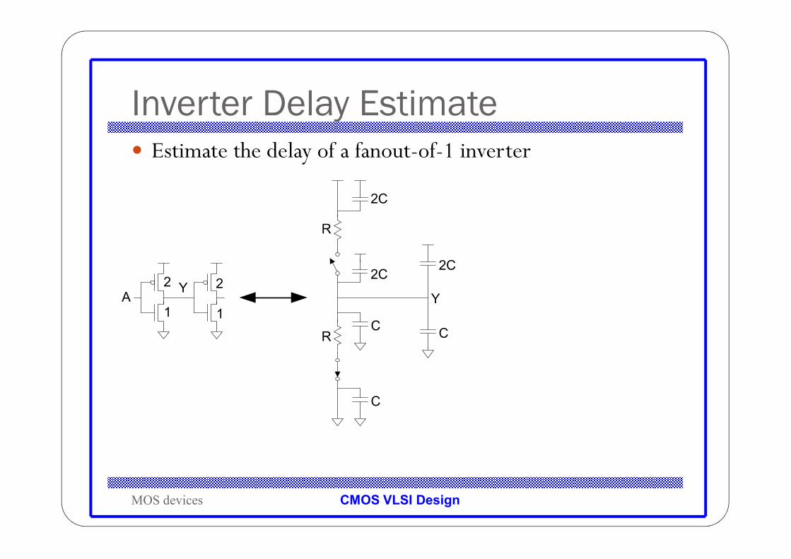
Inverter Delay Estimate
MOS devices
� Estimate the delay of a fanout-of-1 inverter
C
CR
2C
2C
R
2
1A
Y
C
2C
Y2
1
CMOS VLSI Design
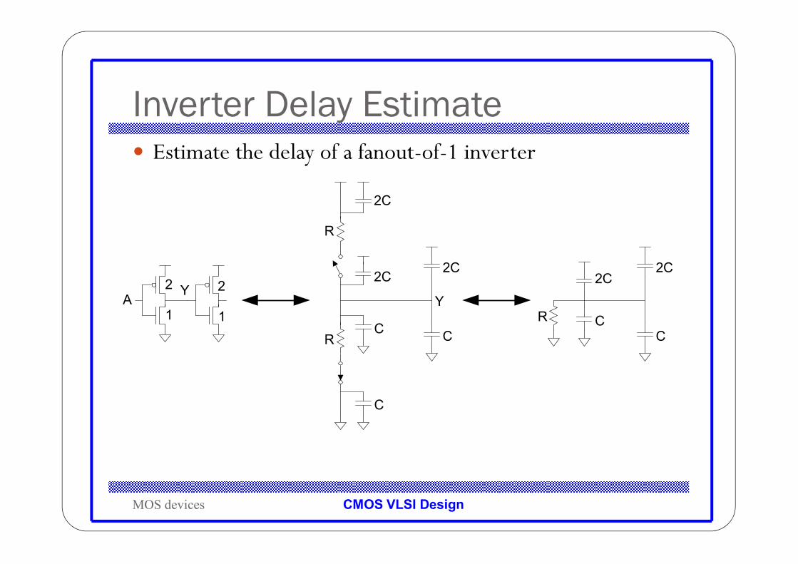
Inverter Delay Estimate
MOS devices
� Estimate the delay of a fanout-of-1 inverter
C
CR
2C
2C
R
2
1A
Y
C
2C
C
2C
C
2C
RY
2
1

CMOS VLSI Design
Inverter Delay Estimate
MOS devices
� Estimate the delay of a fanout-of-1 inverter
C
CR
2C
2C
R
2
1A
Y
C
2C
C
2C
C
2C
RY
2
1
d = 6RC

CMOS VLSI Design
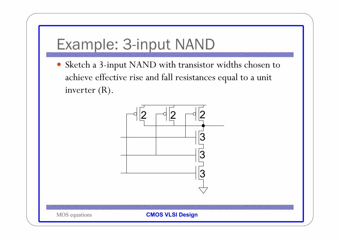
Example: 3-input NAND
MOS equations
� Sketch a 3-input NAND with transistor widths chosen to achieve effective rise and fall resistances equal to a unit inverter (R).

CMOS VLSI Design
Example: 3-input NAND
MOS equations
� Sketch a 3-input NAND with transistor widths chosen to achieve effective rise and fall resistances equal to a unit inverter (R).
CMOS VLSI Design
Example: 3-input NAND
MOS equations
� Sketch a 3-input NAND with transistor widths chosen to achieve effective rise and fall resistances equal to a unit inverter (R).
3
3
222
3

CMOS VLSI Design
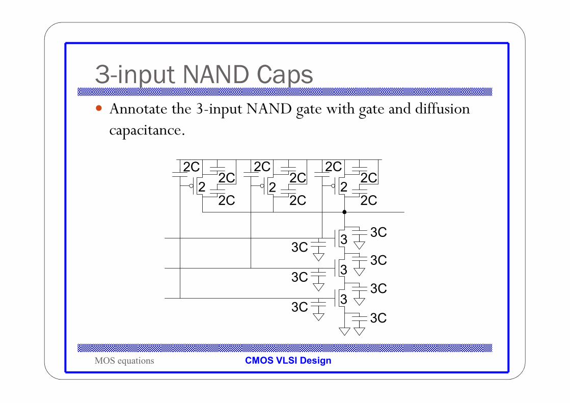
3-input NAND Caps
MOS equations
� Annotate the 3-input NAND gate with gate and diffusion capacitance.
2 2 2
3
3
3
CMOS VLSI Design
3-input NAND Caps
MOS equations
� Annotate the 3-input NAND gate with gate and diffusion capacitance.
2 2 2
3
3
33C
3C
3C
3C
2C
2C
2C
2C
2C
2C
3C
3C
3C
2C 2C 2C
CMOS VLSI Design
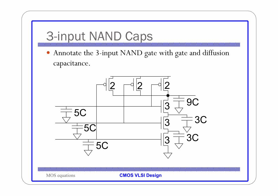
3-input NAND Caps
MOS equations
� Annotate the 3-input NAND gate with gate and diffusion capacitance.
9C
3C
3C3
3
3
222
5C
5C
5C

CMOS VLSI Design
Elmore Delay
MOS equations
� ON transistors look like resistors
� Pullup or pulldown network modeled as RC ladder
� Elmore delay of RC ladder
R1
R2
R3
RN
C1
C2
C3
CN
( ) ( )nodes
1 1 1 2 2 1 2... ...
pd i to source i
i
N N
t R C
RC R R C R R R C
− −≈
= + + + + + + +
∑

CMOS VLSI Design
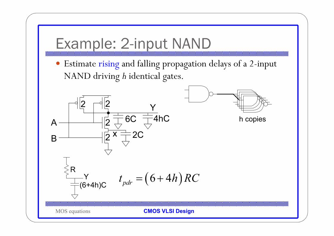
Example: 2-input NAND
MOS equations
� Estimate worst-case rising and falling delay of 2-input NAND driving h identical gates.
h copies
2
2
22
B
A
x
Y
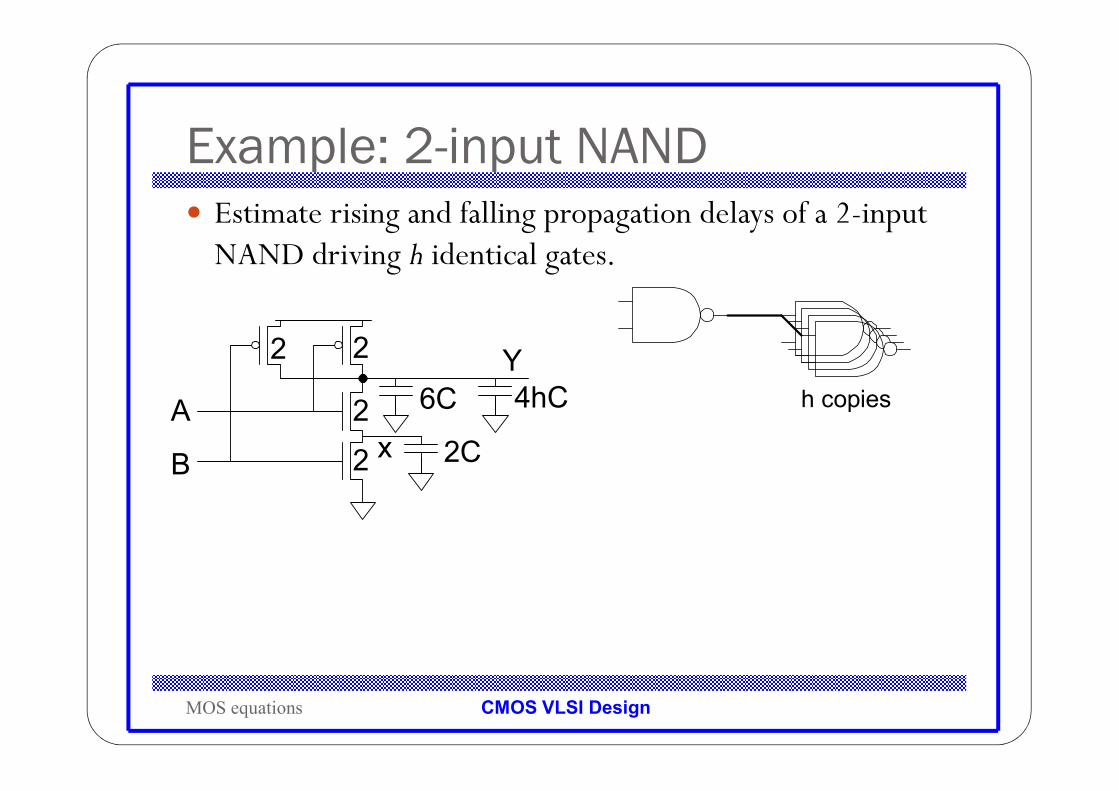
CMOS VLSI Design
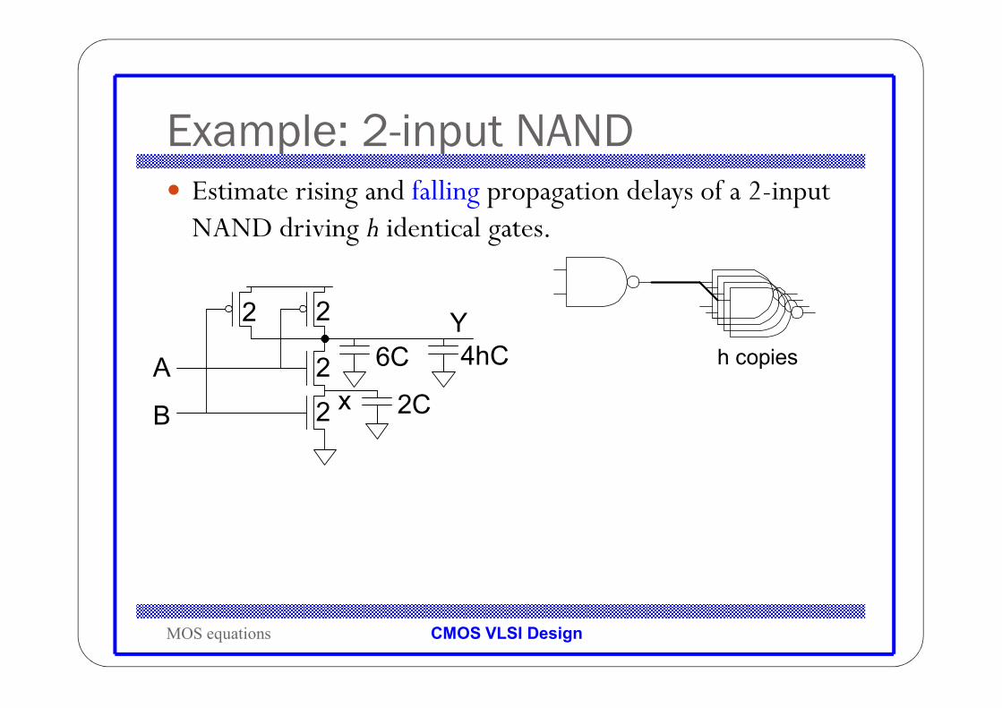
Example: 2-input NAND
MOS equations
� Estimate rising and falling propagation delays of a 2-input NAND driving h identical gates.
h copies6C
2C2
2
22
4hC
B
A
x
Y
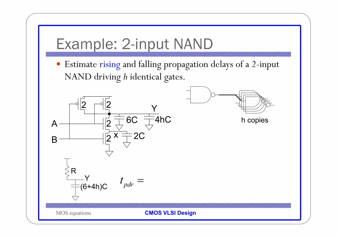
CMOS VLSI Design
Example: 2-input NAND
MOS equations
� Estimate rising and falling propagation delays of a 2-input NAND driving h identical gates.
h copies6C
2C2
2
22
4hC
B
A
x
Y
R
(6+4h)CY
pdrt =
CMOS VLSI Design
Example: 2-input NAND
MOS equations
� Estimate rising and falling propagation delays of a 2-input NAND driving h identical gates.
h copies6C
2C2
2
22
4hC
B
A
x
Y
R
(6+4h)CY ( )6 4pdrt h RC= +
CMOS VLSI Design
Example: 2-input NAND
MOS equations
� Estimate rising and falling propagation delays of a 2-input NAND driving h identical gates.
h copies6C
2C2
2
22
4hC
B
A
x
Y
CMOS VLSI Design
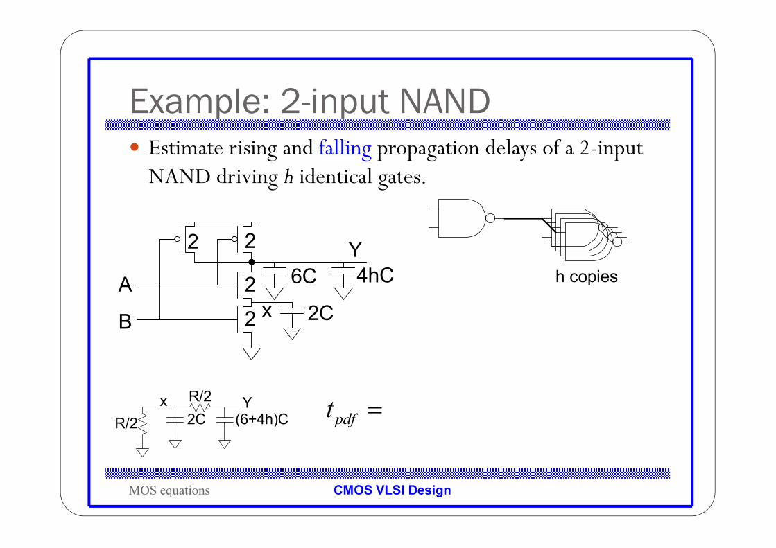
Example: 2-input NAND
MOS equations
� Estimate rising and falling propagation delays of a 2-input NAND driving h identical gates.
h copies6C
2C2
2
22
4hC
B
A
x
Y
pdft =(6+4h)C2CR/2
R/2x Y
CMOS VLSI Design
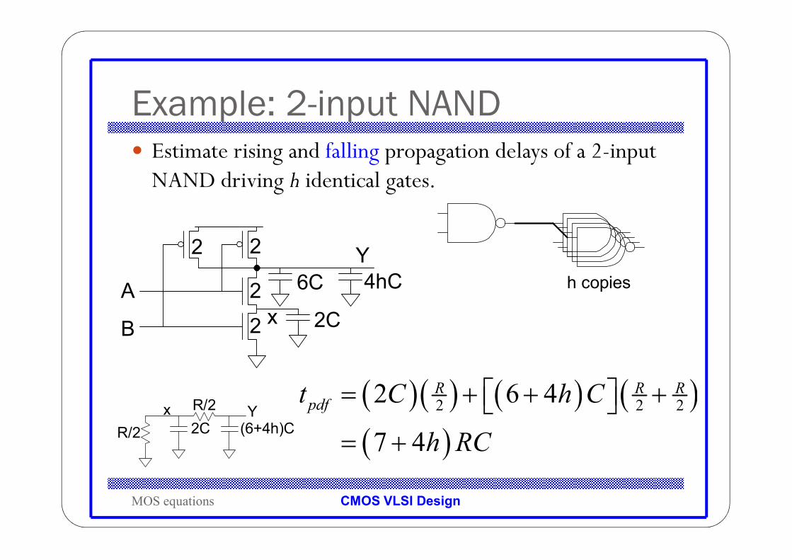
Example: 2-input NAND
MOS equations
� Estimate rising and falling propagation delays of a 2-input NAND driving h identical gates.
h copies6C
2C2
2
22
4hC
B
A
x
Y
( ) ( ) ( ) ( )( )
2 2 22 6 4
7 4
R R Rpdft C h C
h RC
= + + + = +
(6+4h)C2CR/2
R/2x Y
CMOS VLSI Design
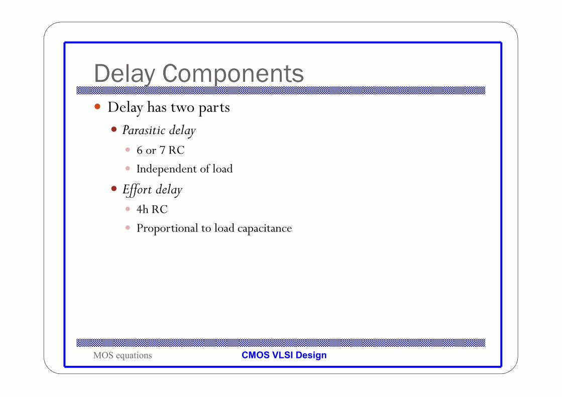
Delay Components
MOS equations
� Delay has two parts� Parasitic delay
� 6 or 7 RC
� Independent of load
� Effort delay� 4h RC
� Proportional to load capacitance

CMOS VLSI Design
Contamination Delay
MOS equations
� Best-case (contamination) delay can be substantially less than propagation delay.
� Ex: If both inputs fall simultaneously
6C
2C2
2
22
4hC
B
A
x
Y
R
(6+4h)CYR
( )3 2cdrt h RC= +