Embed Size (px)
Citation preview
4: DC and Transient Response Slide 1CMOS VLSI Design
EE466: VLSI Design
Lecture 05: DC and transient response – CMOS Inverters
4: DC and Transient Response Slide 2CMOS VLSI Design
Outline DC Response Logic Levels and Noise Margins Transient Response Delay Estimation
4: DC and Transient Response Slide 3CMOS VLSI Design
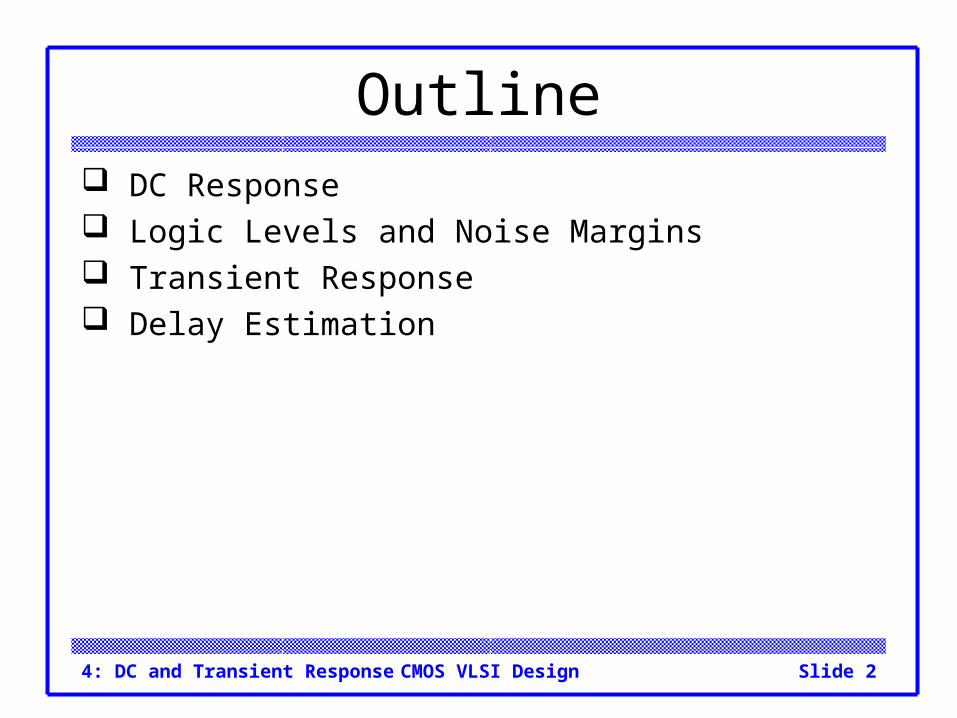
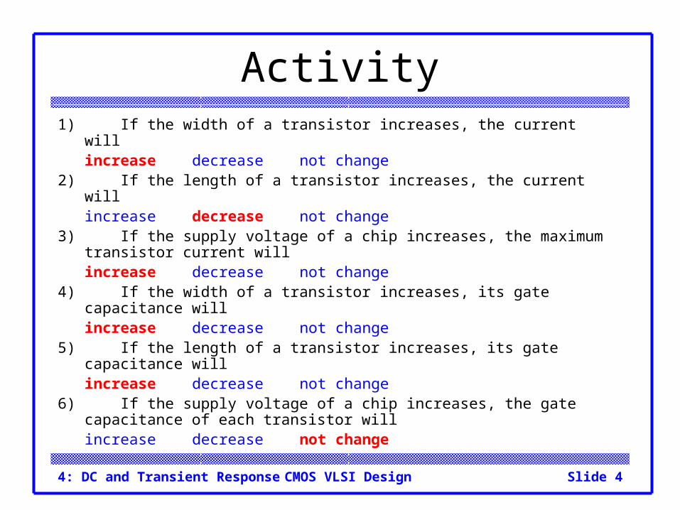
Activity1) If the width of a transistor increases, the current will
increase decrease not change 2) If the length of a transistor increases, the current will
increase decrease not change3) If the supply voltage of a chip increases, the maximum
transistor current willincrease decrease not change
4) If the width of a transistor increases, its gate capacitance willincrease decrease not change
5) If the length of a transistor increases, its gate capacitance willincrease decrease not change
6) If the supply voltage of a chip increases, the gate capacitance of each transistor willincrease decrease not change
4: DC and Transient Response Slide 4CMOS VLSI Design
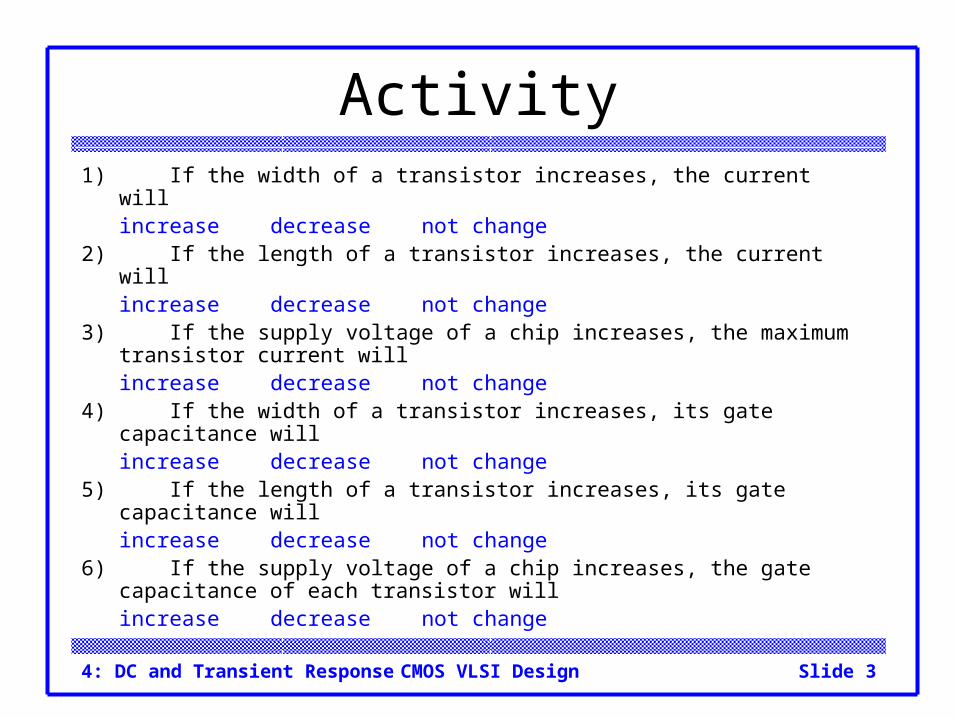
Activity1) If the width of a transistor increases, the current will
increase decrease not change 2) If the length of a transistor increases, the current will
increase decrease not change3) If the supply voltage of a chip increases, the maximum
transistor current willincrease decrease not change
4) If the width of a transistor increases, its gate capacitance willincrease decrease not change
5) If the length of a transistor increases, its gate capacitance willincrease decrease not change
6) If the supply voltage of a chip increases, the gate capacitance of each transistor willincrease decrease not change
4: DC and Transient Response Slide 5CMOS VLSI Design
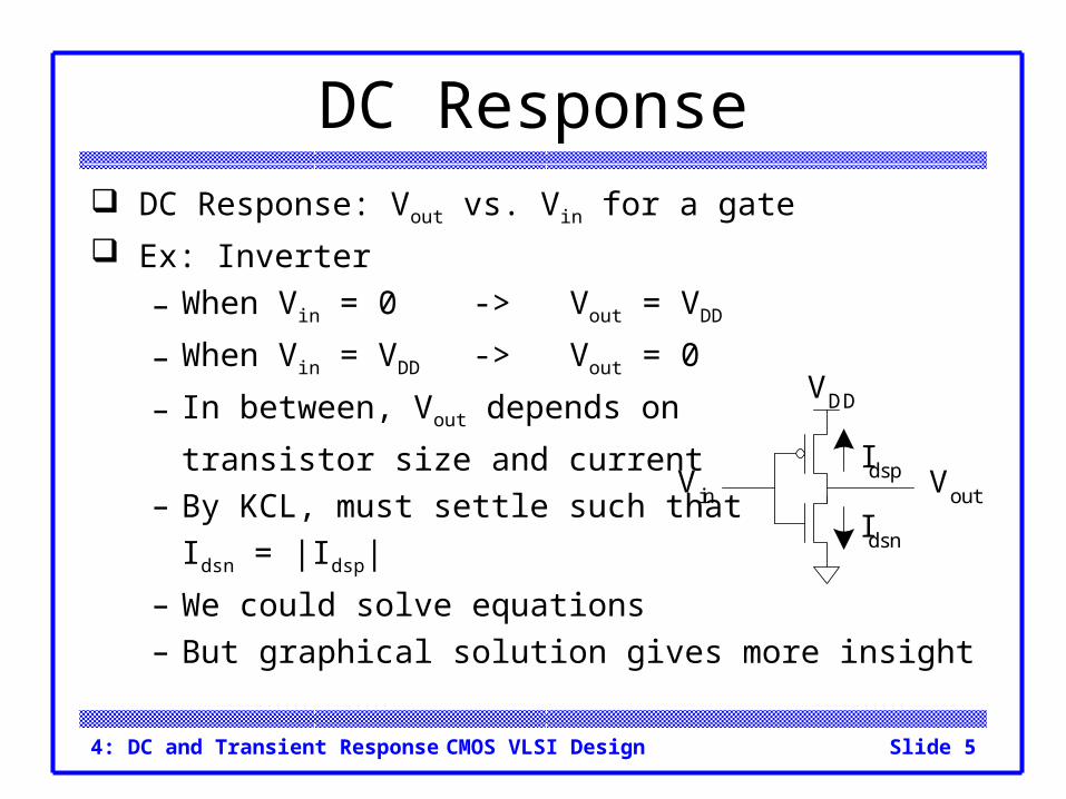
DC Response DC Response: Vout vs. Vin for a gate
Ex: Inverter
– When Vin = 0 -> Vout = VDD
– When Vin = VDD -> Vout = 0
– In between, Vout depends on
transistor size and current– By KCL, must settle such that
Idsn = |Idsp|
– We could solve equations– But graphical solution gives more insight
Idsn
Idsp Vout
VDD
Vin
4: DC and Transient Response Slide 6CMOS VLSI Design
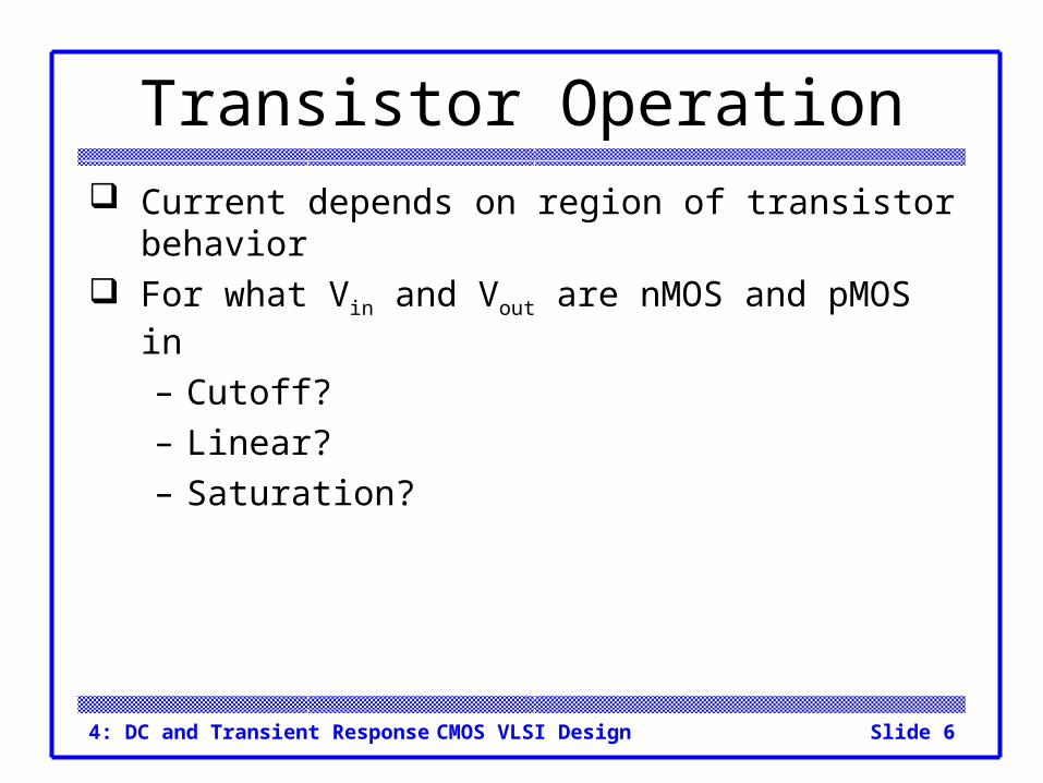
Transistor Operation Current depends on region of transistor behavior For what Vin and Vout are nMOS and pMOS in
– Cutoff?– Linear?– Saturation?
4: DC and Transient Response Slide 7CMOS VLSI Design
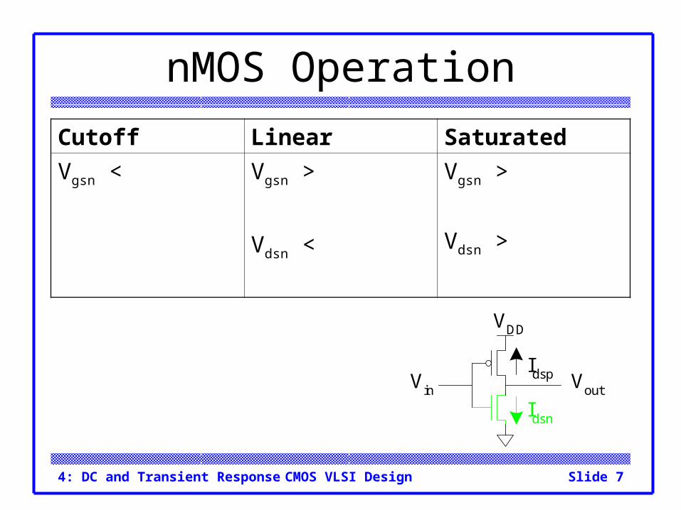
nMOS Operation
Cutoff Linear Saturated
Vgsn < Vgsn >
Vdsn <
Vgsn >
Vdsn >
Idsn
Idsp Vout
VDD
Vin
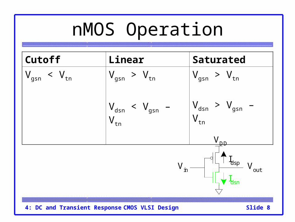
4: DC and Transient Response Slide 8CMOS VLSI Design
nMOS Operation
Cutoff Linear Saturated
Vgsn < Vtn Vgsn > Vtn
Vdsn < Vgsn – Vtn
Vgsn > Vtn
Vdsn > Vgsn – Vtn
Idsn
Idsp Vout
VDD
Vin
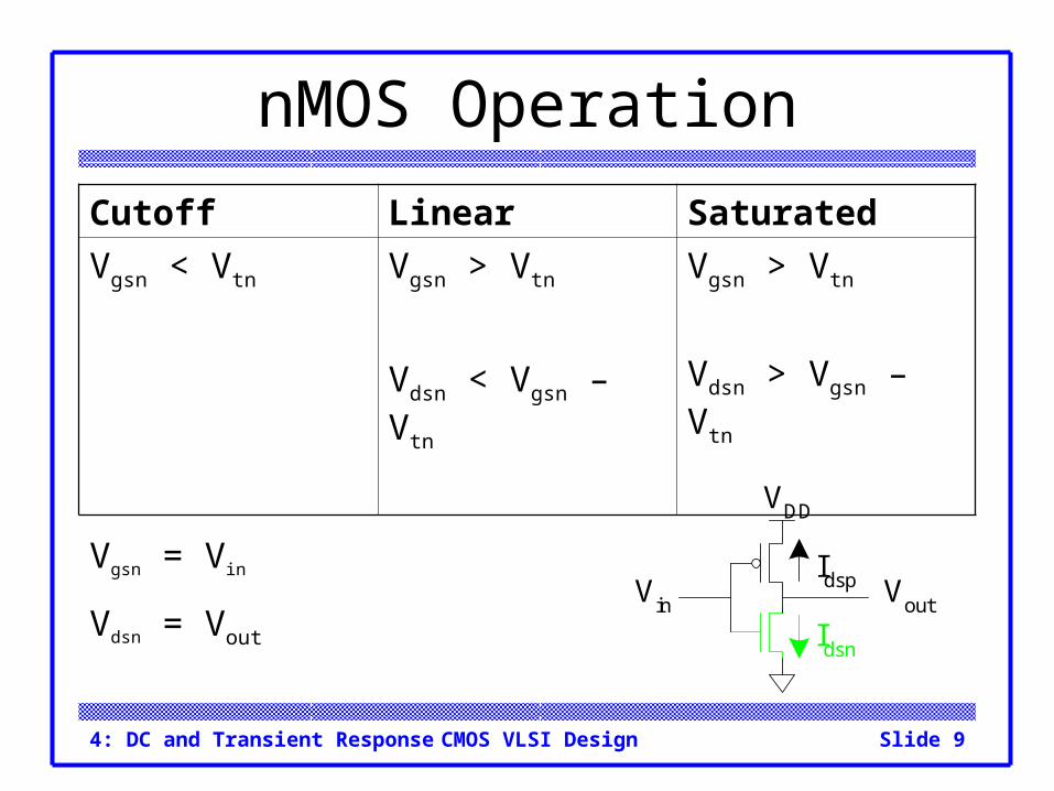
4: DC and Transient Response Slide 9CMOS VLSI Design
nMOS Operation
Cutoff Linear Saturated
Vgsn < Vtn Vgsn > Vtn
Vdsn < Vgsn – Vtn
Vgsn > Vtn
Vdsn > Vgsn – Vtn
Idsn
Idsp Vout
VDD
Vin
Vgsn = Vin
Vdsn = Vout
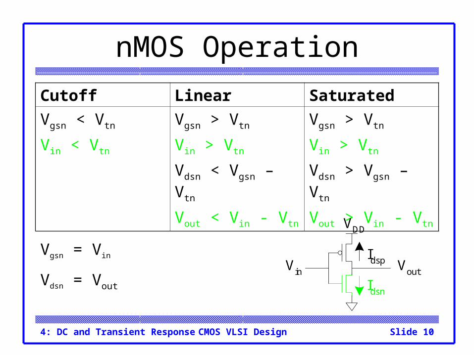
4: DC and Transient Response Slide 10CMOS VLSI Design
nMOS Operation
Cutoff Linear Saturated
Vgsn < Vtn
Vin < Vtn
Vgsn > Vtn
Vin > Vtn
Vdsn < Vgsn – Vtn
Vout < Vin - Vtn
Vgsn > Vtn
Vin > Vtn
Vdsn > Vgsn – Vtn
Vout > Vin - Vtn
Idsn
Idsp Vout
VDD
Vin
Vgsn = Vin
Vdsn = Vout
4: DC and Transient Response Slide 11CMOS VLSI Design
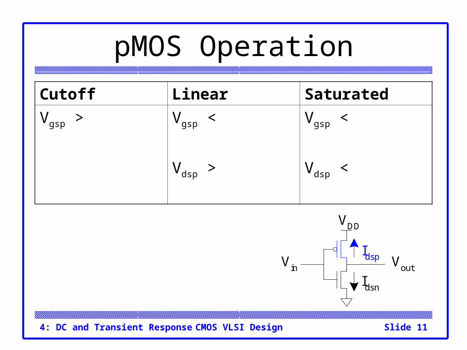
pMOS Operation
Cutoff Linear Saturated
Vgsp > Vgsp <
Vdsp >
Vgsp <
Vdsp <
Idsn
Idsp Vout
VDD
Vin
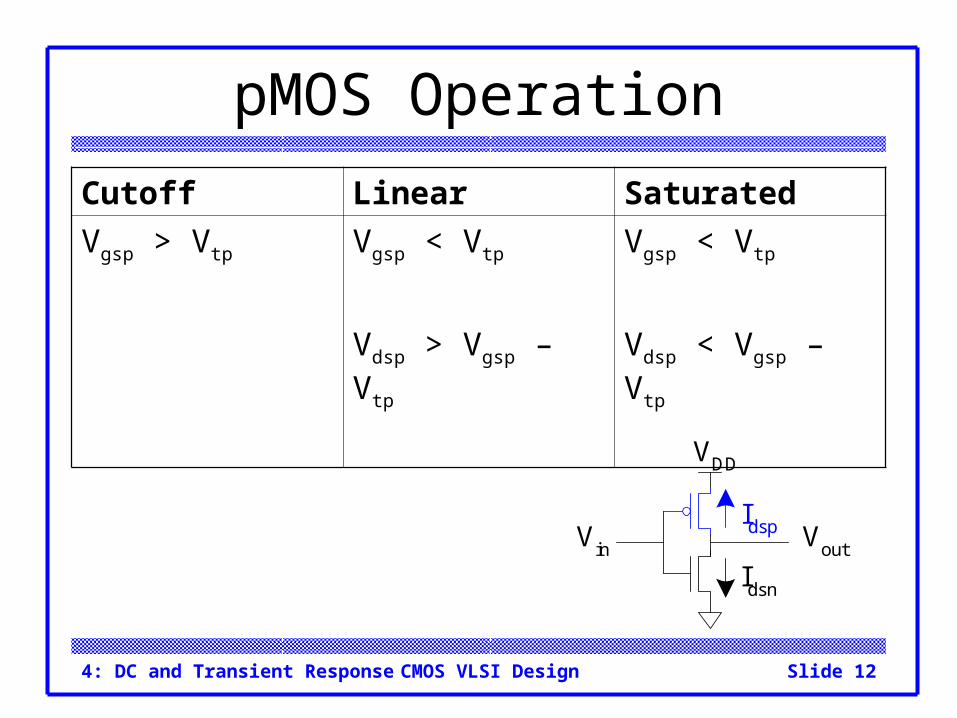
4: DC and Transient Response Slide 12CMOS VLSI Design
pMOS Operation
Cutoff Linear Saturated
Vgsp > Vtp Vgsp < Vtp
Vdsp > Vgsp – Vtp
Vgsp < Vtp
Vdsp < Vgsp – Vtp
Idsn
Idsp Vout
VDD
Vin
4: DC and Transient Response Slide 13CMOS VLSI Design
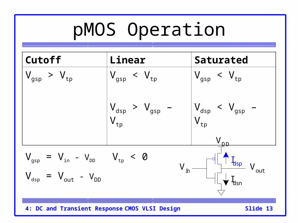
pMOS Operation
Cutoff Linear Saturated
Vgsp > Vtp Vgsp < Vtp
Vdsp > Vgsp – Vtp
Vgsp < Vtp
Vdsp < Vgsp – Vtp
Idsn
Idsp Vout
VDD
Vin
Vgsp = Vin - VDD
Vdsp = Vout - VDD
Vtp < 0
4: DC and Transient Response Slide 14CMOS VLSI Design
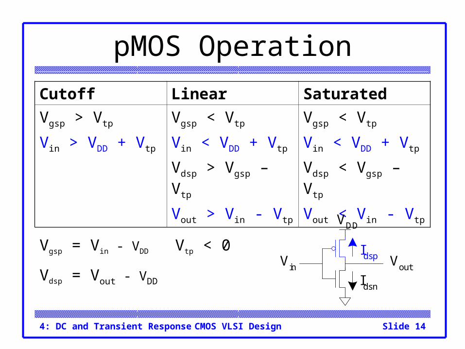
pMOS Operation
Cutoff Linear Saturated
Vgsp > Vtp
Vin > VDD + Vtp
Vgsp < Vtp
Vin < VDD + Vtp
Vdsp > Vgsp – Vtp
Vout > Vin - Vtp
Vgsp < Vtp
Vin < VDD + Vtp
Vdsp < Vgsp – Vtp
Vout < Vin - Vtp
Idsn
Idsp Vout
VDD
Vin
Vgsp = Vin - VDD
Vdsp = Vout - VDD
Vtp < 0
4: DC and Transient Response Slide 15CMOS VLSI Design
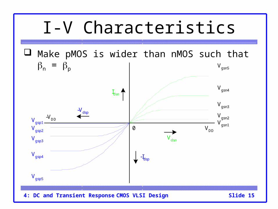
I-V Characteristics Make pMOS is wider than nMOS such that n = p
Vgsn5
Vgsn4
Vgsn3
Vgsn2Vgsn1
Vgsp5
Vgsp4
Vgsp3
Vgsp2
Vgsp1
VDD
-VDD
Vdsn
-Vdsp
-Idsp
Idsn
0
4: DC and Transient Response Slide 16CMOS VLSI Design
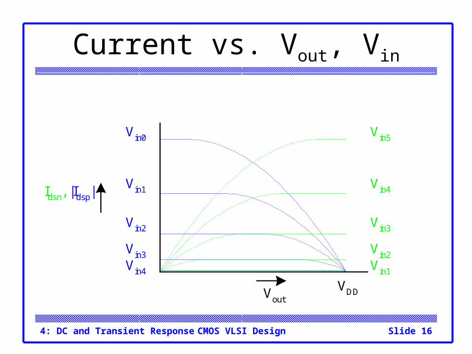
Current vs. Vout, Vin
Vin5
Vin4
Vin3
Vin2Vin1
Vin0
Vin1
Vin2
Vin3Vin4
Idsn, |Idsp|
VoutVDD
4: DC and Transient Response Slide 17CMOS VLSI Design
Load Line Analysis
Vin5
Vin4
Vin3
Vin2Vin1
Vin0
Vin1
Vin2
Vin3Vin4
Idsn, |Idsp|
VoutVDD
For a given Vin:
– Plot Idsn, Idsp vs. Vout
– Vout must be where |currents| are equal in
Idsn
Idsp Vout
VDD
Vin
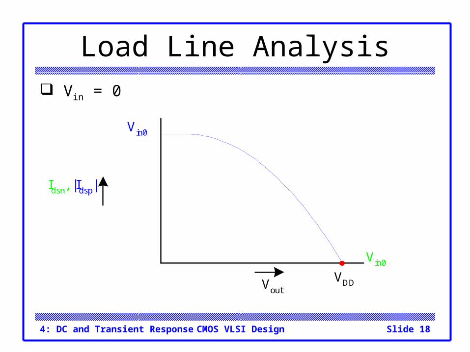
4: DC and Transient Response Slide 18CMOS VLSI Design
Load Line Analysis
Vin0
Vin0
Idsn, |Idsp|
VoutVDD
Vin = 0
4: DC and Transient Response Slide 19CMOS VLSI Design
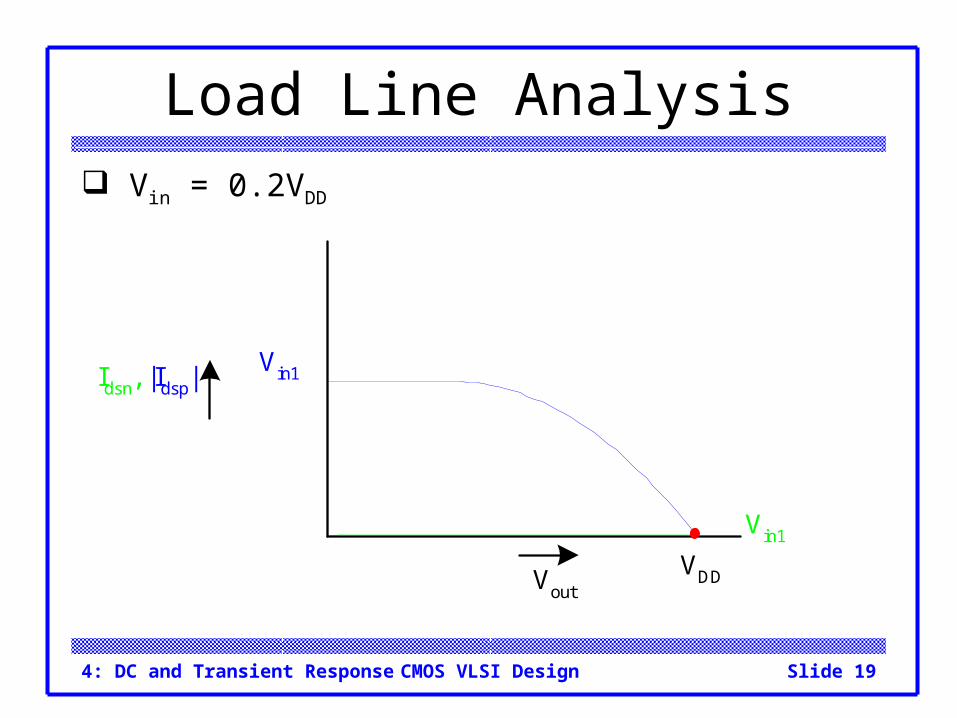
Load Line Analysis
Vin1
Vin1Idsn, |Idsp|
VoutVDD
Vin = 0.2VDD
4: DC and Transient Response Slide 20CMOS VLSI Design
Load Line Analysis
Vin2
Vin2
Idsn, |Idsp|
VoutVDD
Vin = 0.4VDD
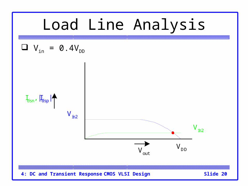
4: DC and Transient Response Slide 21CMOS VLSI Design
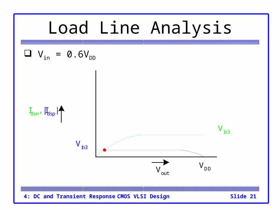
Load Line Analysis
Vin3
Vin3
Idsn, |Idsp|
VoutVDD
Vin = 0.6VDD
4: DC and Transient Response Slide 22CMOS VLSI Design
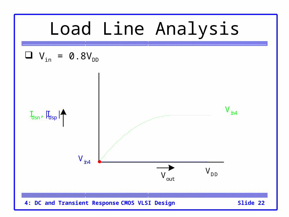
Load Line Analysis
Vin4
Vin4
Idsn, |Idsp|
VoutVDD
Vin = 0.8VDD
4: DC and Transient Response Slide 23CMOS VLSI Design
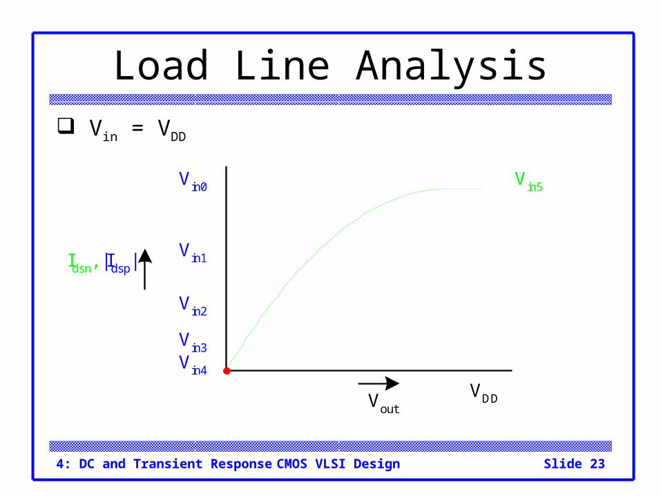
Load Line Analysis
Vin5Vin0
Vin1
Vin2
Vin3Vin4
Idsn, |Idsp|
VoutVDD
Vin = VDD
4: DC and Transient Response Slide 24CMOS VLSI Design
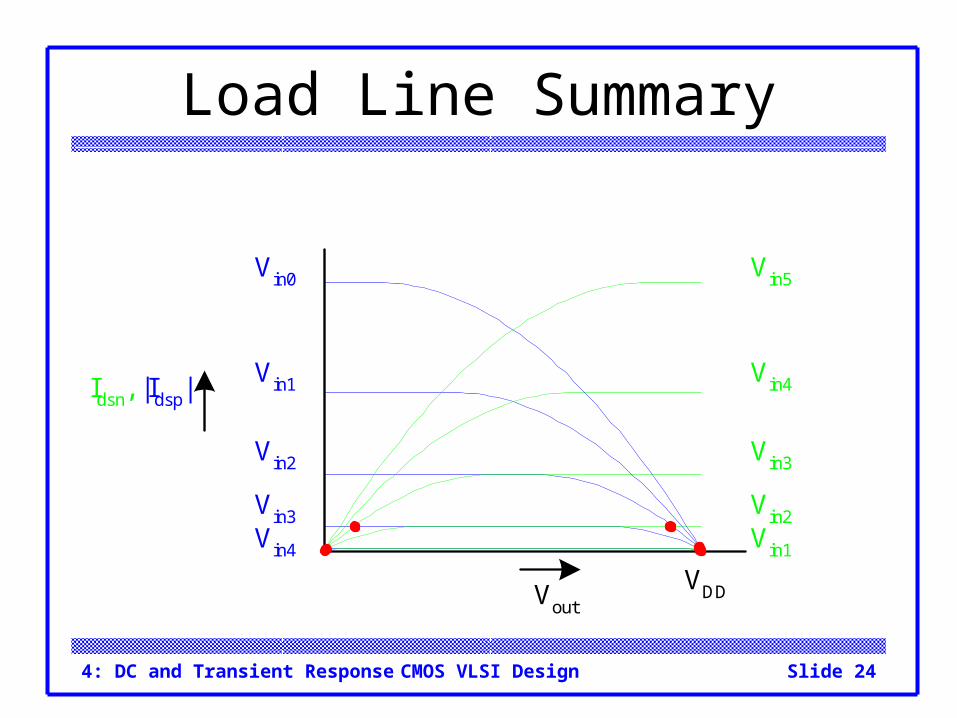
Load Line Summary
Vin5
Vin4
Vin3
Vin2Vin1
Vin0
Vin1
Vin2
Vin3Vin4
Idsn, |Idsp|
VoutVDD
4: DC and Transient Response Slide 25CMOS VLSI Design
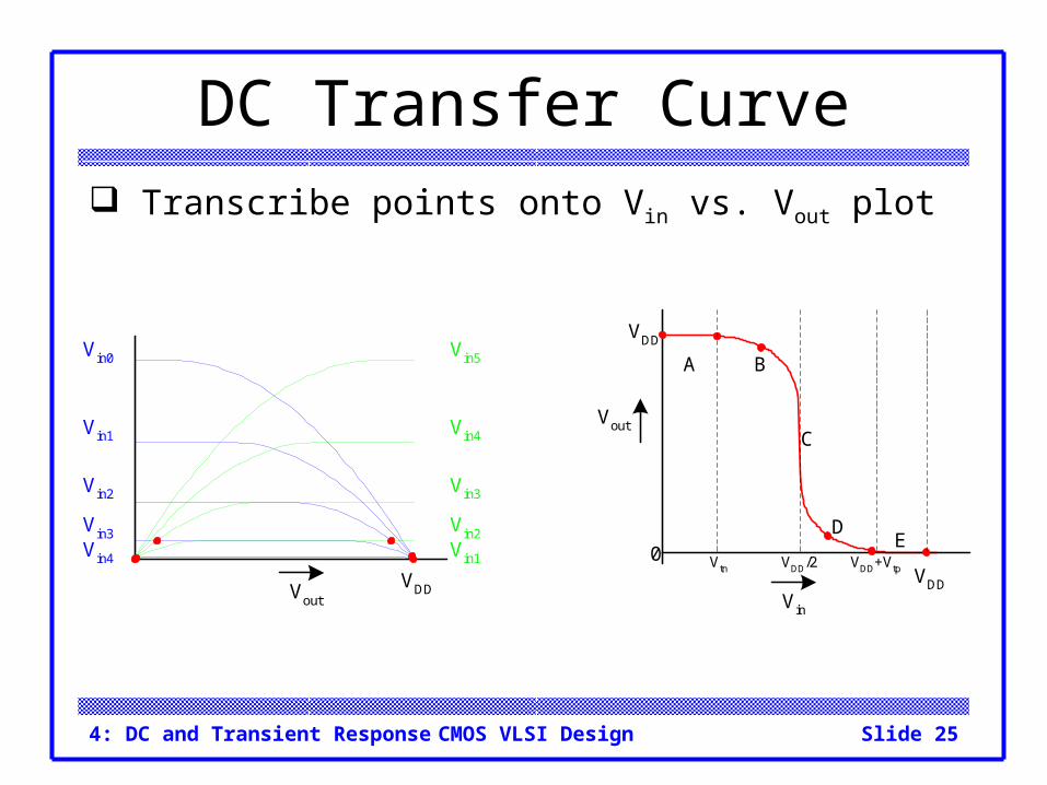
DC Transfer Curve Transcribe points onto Vin vs. Vout plot
Vin5
Vin4
Vin3
Vin2Vin1
Vin0
Vin1
Vin2
Vin3Vin4
VoutVDD
CVout
0
Vin
VDD
VDD
A B
DE
Vtn VDD/2 VDD+Vtp
4: DC and Transient Response Slide 26CMOS VLSI Design
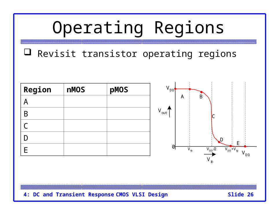
Operating Regions Revisit transistor operating regions
CVout
0
Vin
VDD
VDD
A B
DE
Vtn VDD/2 VDD+Vtp
Region nMOS pMOS
A
B
C
D
E
4: DC and Transient Response Slide 27CMOS VLSI Design
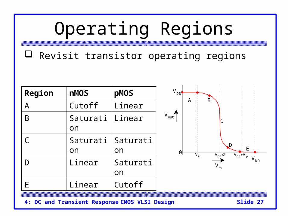
Operating Regions Revisit transistor operating regions
CVout
0
Vin
VDD
VDD
A B
DE
Vtn VDD/2 VDD+Vtp
Region nMOS pMOS
A Cutoff Linear
B Saturation Linear
C Saturation Saturation
D Linear Saturation
E Linear Cutoff
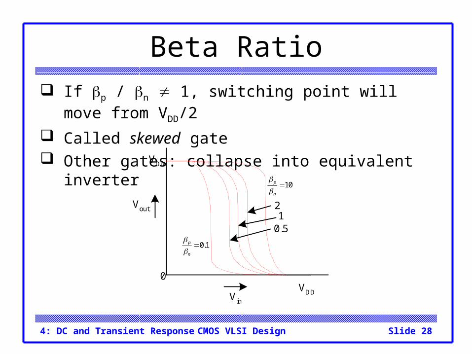
4: DC and Transient Response Slide 28CMOS VLSI Design
Beta Ratio If p / n 1, switching point will move from VDD/2
Called skewed gate Other gates: collapse into equivalent inverter
Vout
0
Vin
VDD
VDD
0.51
2
10p
n
0.1p
n
4: DC and Transient Response Slide 29CMOS VLSI Design
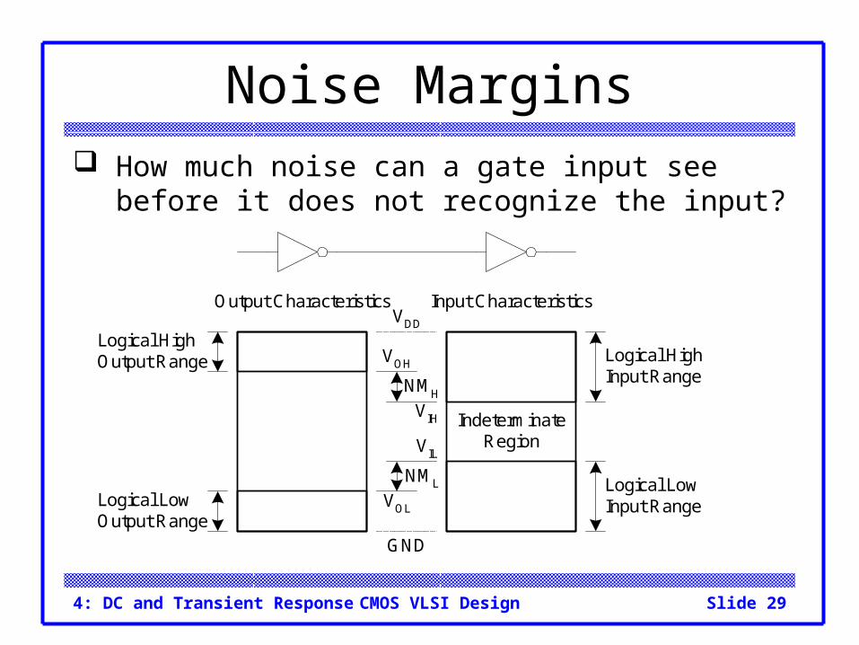
Noise Margins How much noise can a gate input see before it does
not recognize the input?
IndeterminateRegion
NML
NMH
Input CharacteristicsOutput Characteristics
VOH
VDD
VOL
GND
VIH
VIL
Logical HighInput Range
Logical LowInput Range
Logical HighOutput Range
Logical LowOutput Range
4: DC and Transient Response Slide 30CMOS VLSI Design
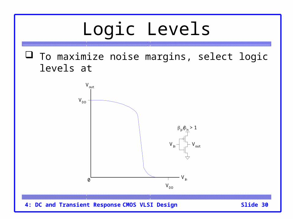
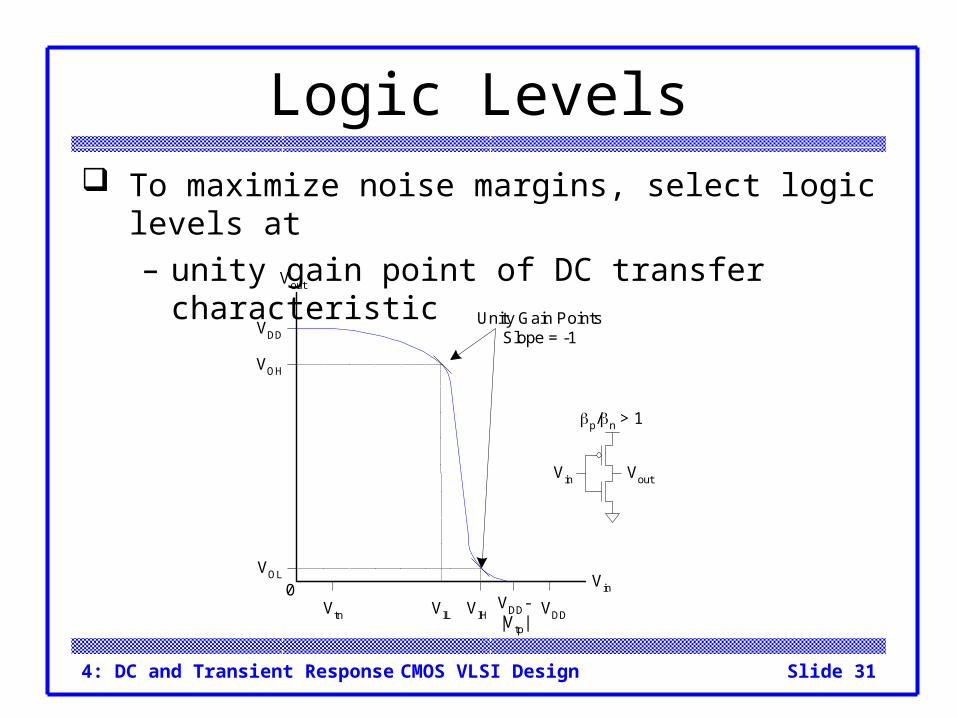
Logic Levels To maximize noise margins, select logic levels at
VDD
Vin
Vout
VDD
p/n > 1
Vin Vout
0
4: DC and Transient Response Slide 31CMOS VLSI Design
Logic Levels To maximize noise margins, select logic levels at
– unity gain point of DC transfer characteristic
VDD
Vin
Vout
VOH
VDD
VOL
VIL VIHVtn
Unity Gain PointsSlope = -1
VDD-|Vtp|
p/n > 1
Vin Vout
0
4: DC and Transient Response Slide 32CMOS VLSI Design
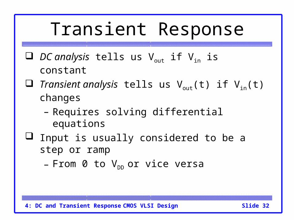
Transient Response DC analysis tells us Vout if Vin is constant
Transient analysis tells us Vout(t) if Vin(t) changes
– Requires solving differential equations Input is usually considered to be a step or ramp
– From 0 to VDD or vice versa
4: DC and Transient Response Slide 33CMOS VLSI Design
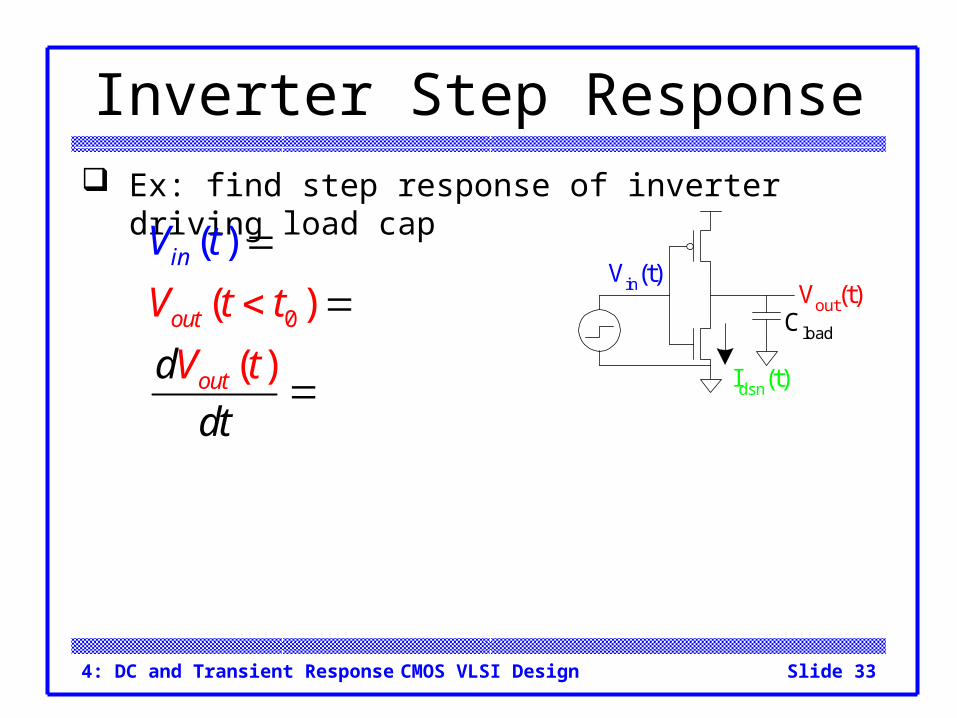
Inverter Step Response Ex: find step response of inverter driving load cap
0( )
(
)
)
(o
i
ut
n
out
V t t
t
V
t
V
d
d
t
Vin(t) Vout(t)Cload
Idsn(t)
4: DC and Transient Response Slide 34CMOS VLSI Design
Inverter Step Response Ex: find step response of inverter driving load cap
0
0
( )
( )
( )
( )
ou
DDin
t
out
u t t V
d
d
t
t t
V t
V
V
t
Vin(t) Vout(t)Cload
Idsn(t)
4: DC and Transient Response Slide 35CMOS VLSI Design
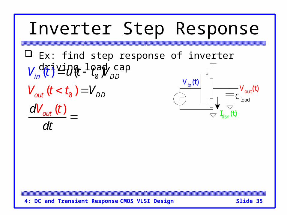
Inverter Step Response Ex: find step response of inverter driving load cap
0
0(
( ))
(
(
)
)
DD
Do
i
D
o t
n
ut
u
V t
u t t V
V
d
d
t
t
V
V
t
t
Vin(t) Vout(t)Cload
Idsn(t)
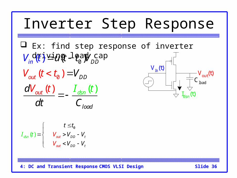
4: DC and Transient Response Slide 36CMOS VLSI Design
Inverter Step Response Ex: find step response of inverter driving load cap
0
0
( )
( )
( )
(
(
)
)
DD
DD
loa
d
ou
i
d
t
o
n
ut sn
V
V
u t t V
t t
V t
V
d
dt C
t
I t
0
( ) DD tout
ou
ds
t DD t
nI t V V
VV V
V
t t
Vin(t) Vout(t)Cload
Idsn(t)
4: DC and Transient Response Slide 37CMOS VLSI Design
Inverter Step Response Ex: find step response of inverter driving load cap
0
0
( )
( )
( )
(
(
)
)
DD
DD
loa
d
ou
i
d
t
o
n
ut sn
V
V
u t t V
t t
V t
V
d
dt C
t
I t
0
2
2
0
2)
)
( ( )
( DD DD t
DD
out
outout out D t
n
t
ds
D
I V
t t
V V V V
V V V VV
t
V t V t
Vin(t) Vout(t)Cload
Idsn(t)
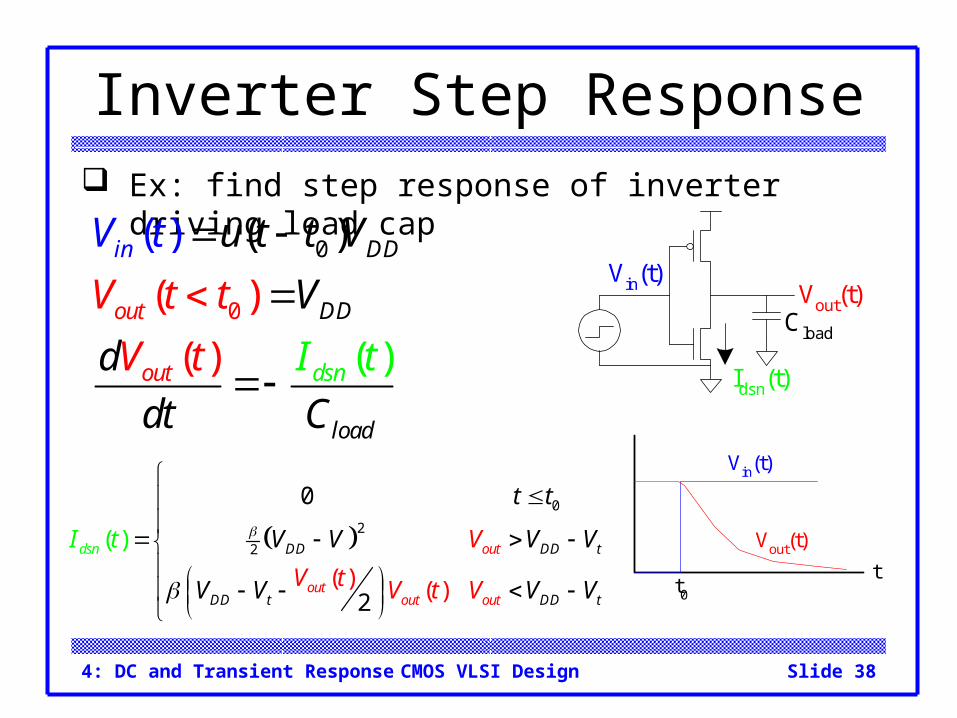
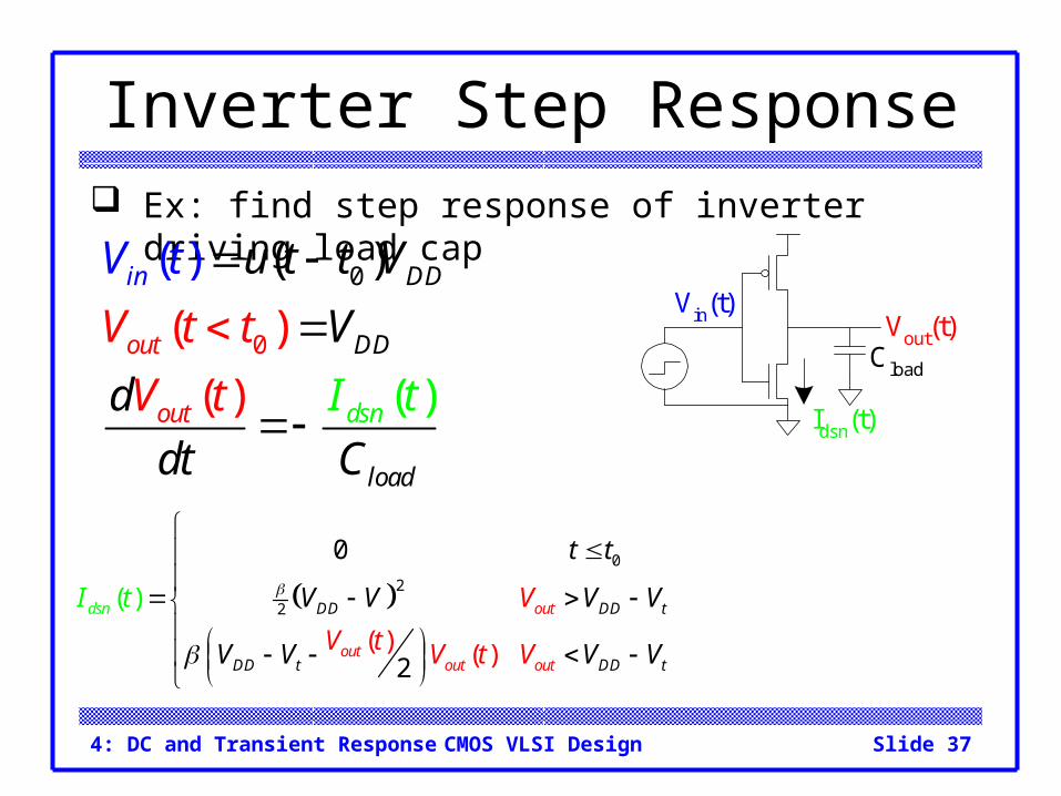
4: DC and Transient Response Slide 38CMOS VLSI Design
Inverter Step Response Ex: find step response of inverter driving load cap
0
0
( )
( )
( )
(
(
)
)
DD
DD
loa
d
ou
i
d
t
o
n
ut sn
V
V
u t t V
t t
V t
V
d
dt C
t
I t
0
2
2
0
2)
)
( ( )
( DD DD t
DD
out
outout out D t
n
t
ds
D
I V
t t
V V V V
V V V VV
t
V t V t
Vout(t)
Vin(t)
t0t
Vin(t) Vout(t)Cload
Idsn(t)
4: DC and Transient Response Slide 39CMOS VLSI Design
Delay Definitions tpdr:
tpdf:
tpd:
tr:
tf: fall time
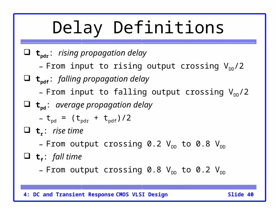
4: DC and Transient Response Slide 40CMOS VLSI Design
Delay Definitions tpdr: rising propagation delay
– From input to rising output crossing VDD/2
tpdf: falling propagation delay
– From input to falling output crossing VDD/2
tpd: average propagation delay
– tpd = (tpdr + tpdf)/2
tr: rise time
– From output crossing 0.2 VDD to 0.8 VDD
tf: fall time
– From output crossing 0.8 VDD to 0.2 VDD
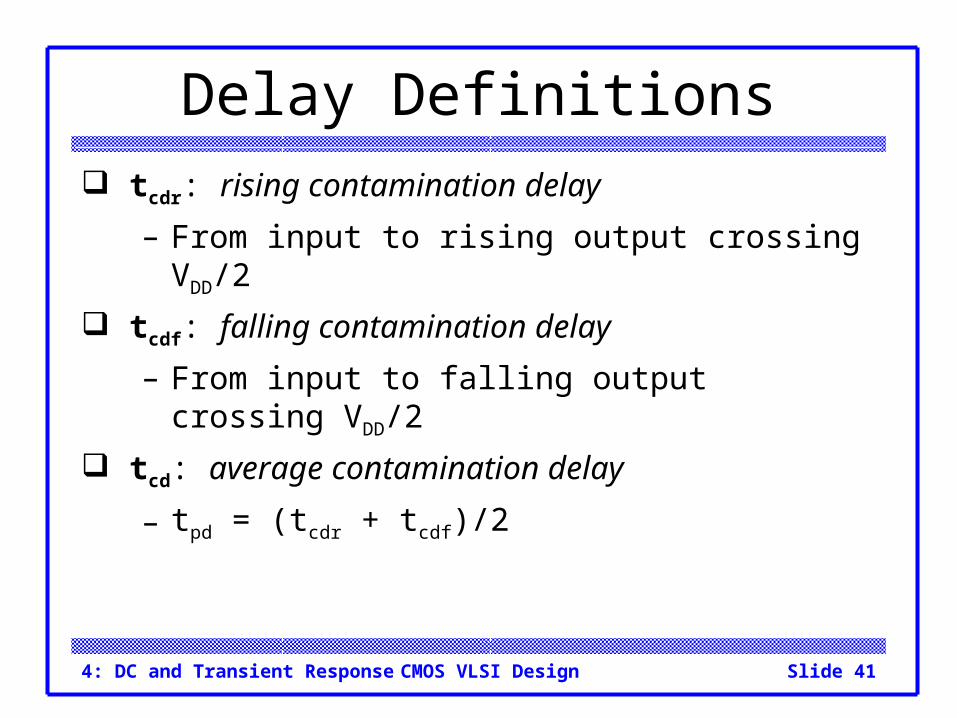
4: DC and Transient Response Slide 41CMOS VLSI Design
Delay Definitions tcdr: rising contamination delay
– From input to rising output crossing VDD/2
tcdf: falling contamination delay
– From input to falling output crossing VDD/2
tcd: average contamination delay
– tpd = (tcdr + tcdf)/2
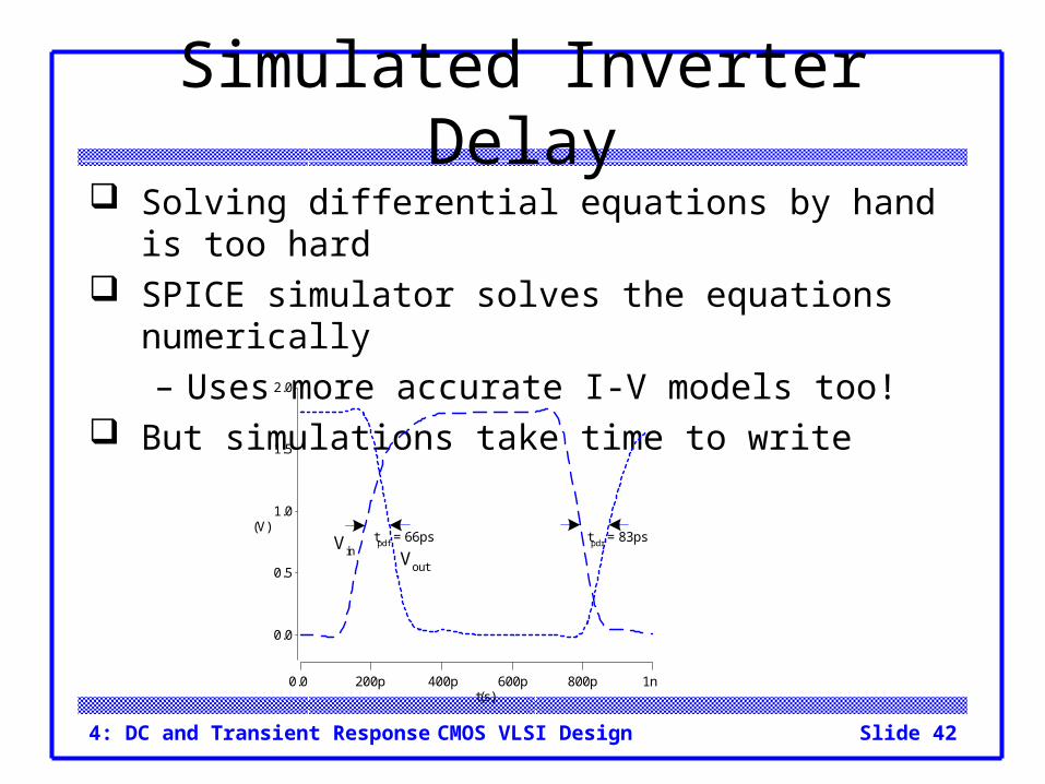
4: DC and Transient Response Slide 42CMOS VLSI Design
Simulated Inverter Delay Solving differential equations by hand is too hard SPICE simulator solves the equations numerically
– Uses more accurate I-V models too! But simulations take time to write
(V)
0.0
0.5
1.0
1.5
2.0
t(s)0.0 200p 400p 600p 800p 1n
tpdf = 66ps tpdr = 83psVin Vout
4: DC and Transient Response Slide 43CMOS VLSI Design
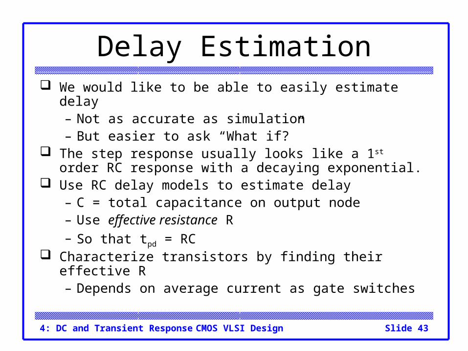
Delay Estimation We would like to be able to easily estimate delay
– Not as accurate as simulation– But easier to ask “What if?”
The step response usually looks like a 1st order RC response with a decaying exponential.
Use RC delay models to estimate delay– C = total capacitance on output node– Use effective resistance R– So that tpd = RC
Characterize transistors by finding their effective R– Depends on average current as gate switches
4: DC and Transient Response Slide 44CMOS VLSI Design
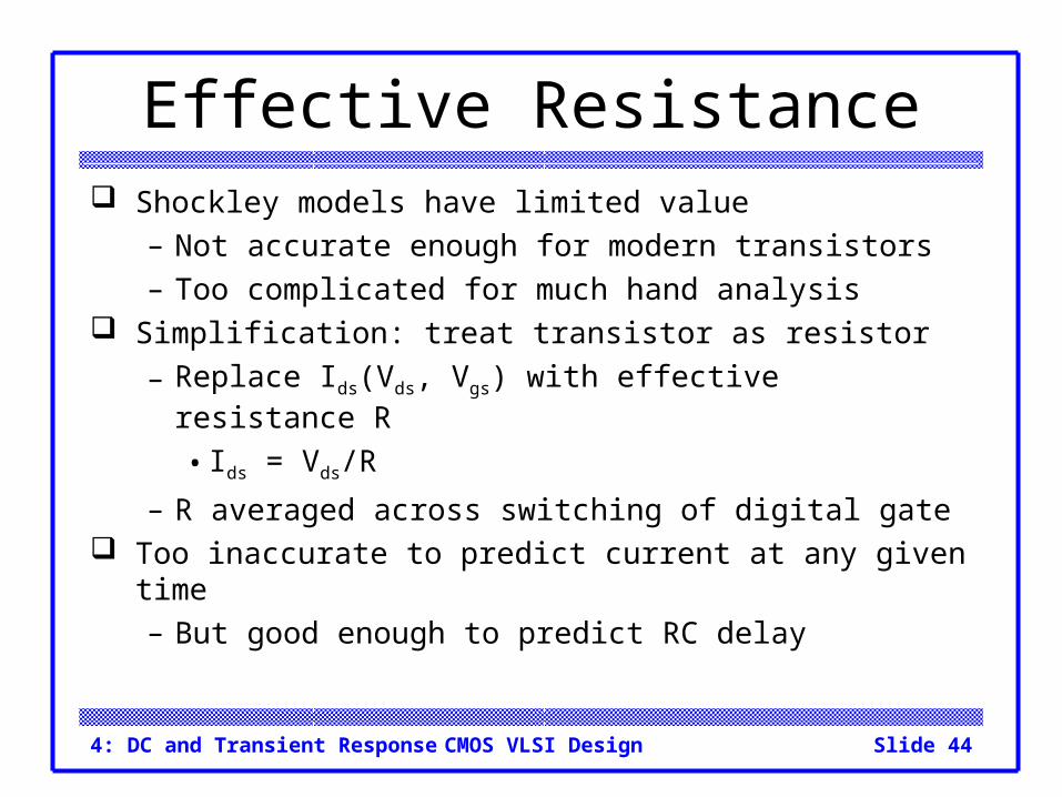
Effective Resistance Shockley models have limited value
– Not accurate enough for modern transistors– Too complicated for much hand analysis
Simplification: treat transistor as resistor
– Replace Ids(Vds, Vgs) with effective resistance R
• Ids = Vds/R
– R averaged across switching of digital gate Too inaccurate to predict current at any given time
– But good enough to predict RC delay
4: DC and Transient Response Slide 45CMOS VLSI Design
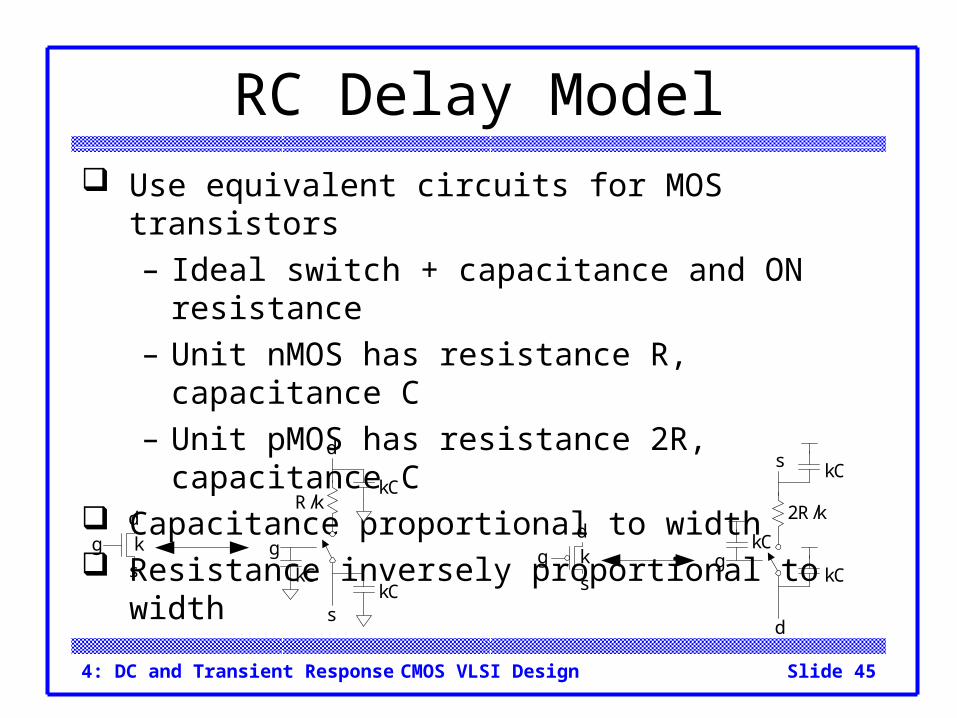
RC Delay Model Use equivalent circuits for MOS transistors
– Ideal switch + capacitance and ON resistance– Unit nMOS has resistance R, capacitance C– Unit pMOS has resistance 2R, capacitance C
Capacitance proportional to width Resistance inversely proportional to width
kg
s
d
g
s
d
kCkC
kCR/k
kg
s
d
g
s
d
kC
kC
kC
2R/k
4: DC and Transient Response Slide 46CMOS VLSI Design
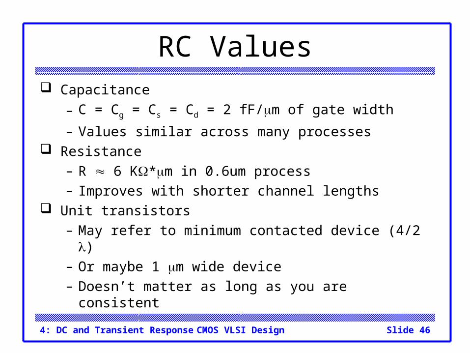
RC Values Capacitance
– C = Cg = Cs = Cd = 2 fF/m of gate width
– Values similar across many processes Resistance
– R 6 K*m in 0.6um process– Improves with shorter channel lengths
Unit transistors– May refer to minimum contacted device (4/2 )– Or maybe 1 m wide device– Doesn’t matter as long as you are consistent
4: DC and Transient Response Slide 47CMOS VLSI Design
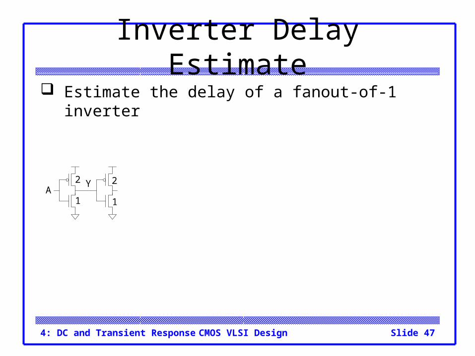
Inverter Delay Estimate Estimate the delay of a fanout-of-1 inverter
2
1A
Y 2
1
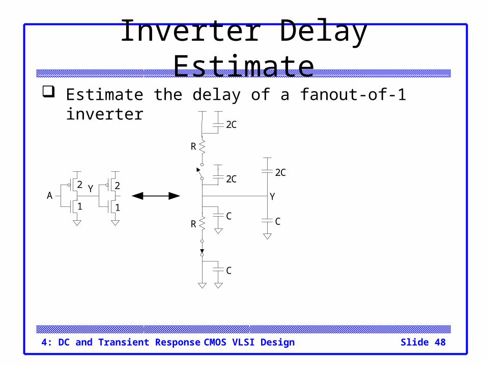
4: DC and Transient Response Slide 48CMOS VLSI Design
Inverter Delay Estimate Estimate the delay of a fanout-of-1 inverter
C
CR
2C
2C
R
2
1A
Y
C
2C
Y2
1
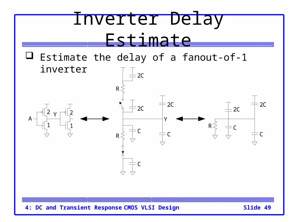
4: DC and Transient Response Slide 49CMOS VLSI Design
Inverter Delay Estimate Estimate the delay of a fanout-of-1 inverter
C
CR
2C
2C
R
2
1A
Y
C
2C
C
2C
C
2C
RY
2
1
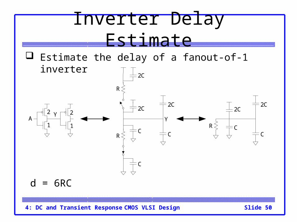
4: DC and Transient Response Slide 50CMOS VLSI Design
Inverter Delay Estimate Estimate the delay of a fanout-of-1 inverter
C
CR
2C
2C
R
2
1A
Y
C
2C
C
2C
C
2C
RY
2
1
d = 6RC

4: DC and Transient Response Slide 51CMOS VLSI Design
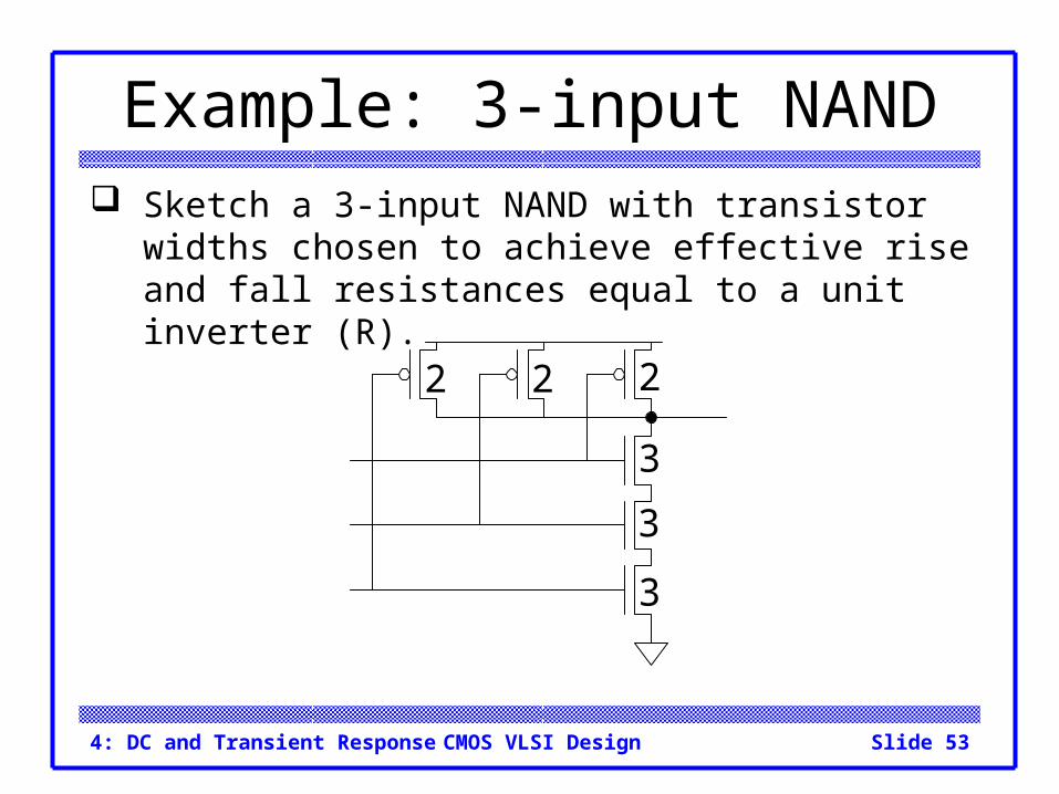
Example: 3-input NAND Sketch a 3-input NAND with transistor widths chosen
to achieve effective rise and fall resistances equal to a unit inverter (R).
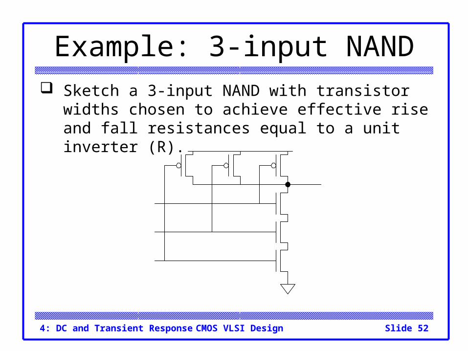
4: DC and Transient Response Slide 52CMOS VLSI Design
Example: 3-input NAND Sketch a 3-input NAND with transistor widths chosen
to achieve effective rise and fall resistances equal to a unit inverter (R).
4: DC and Transient Response Slide 53CMOS VLSI Design
Example: 3-input NAND Sketch a 3-input NAND with transistor widths chosen
to achieve effective rise and fall resistances equal to a unit inverter (R).
3
3
222
3
4: DC and Transient Response Slide 54CMOS VLSI Design
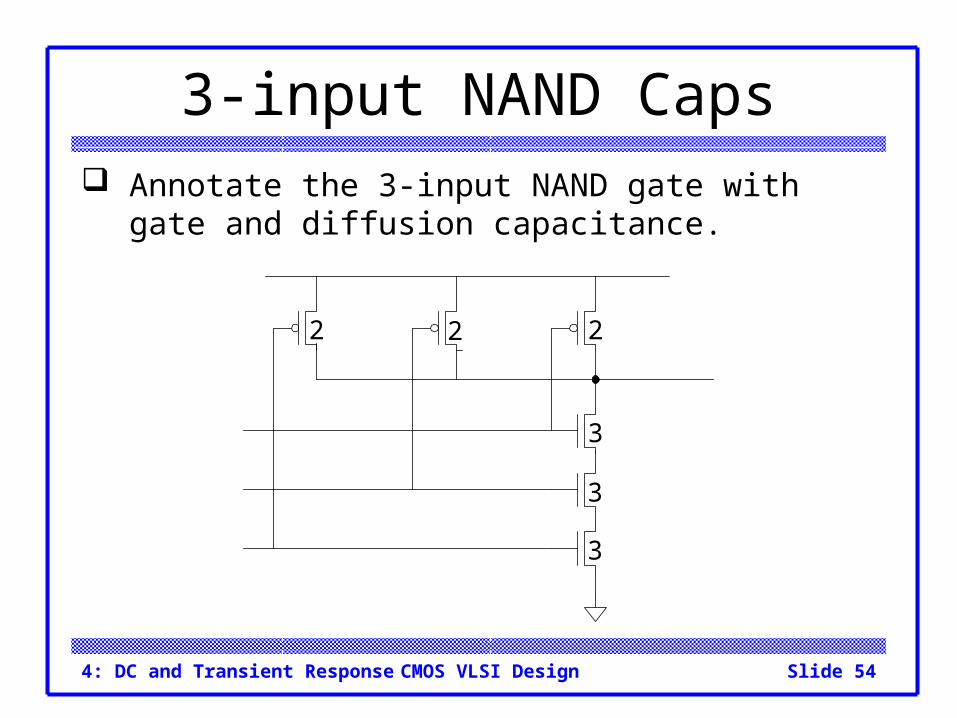
3-input NAND Caps Annotate the 3-input NAND gate with gate and
diffusion capacitance.
2 2 2
3
3
3
4: DC and Transient Response Slide 55CMOS VLSI Design
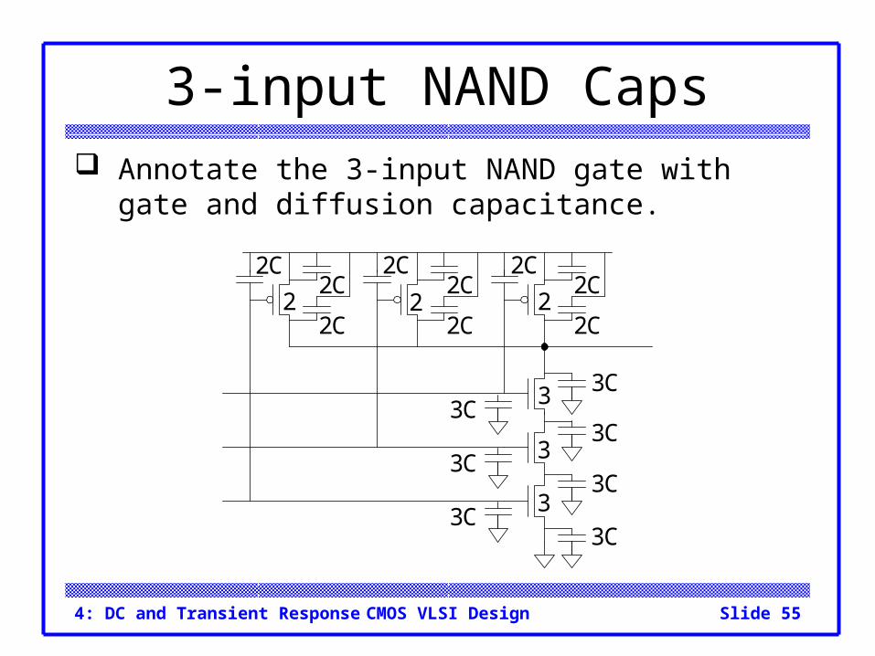
3-input NAND Caps Annotate the 3-input NAND gate with gate and
diffusion capacitance.
2 2 2
3
3
33C
3C
3C
3C
2C
2C
2C
2C
2C
2C
3C
3C
3C
2C 2C 2C
4: DC and Transient Response Slide 56CMOS VLSI Design
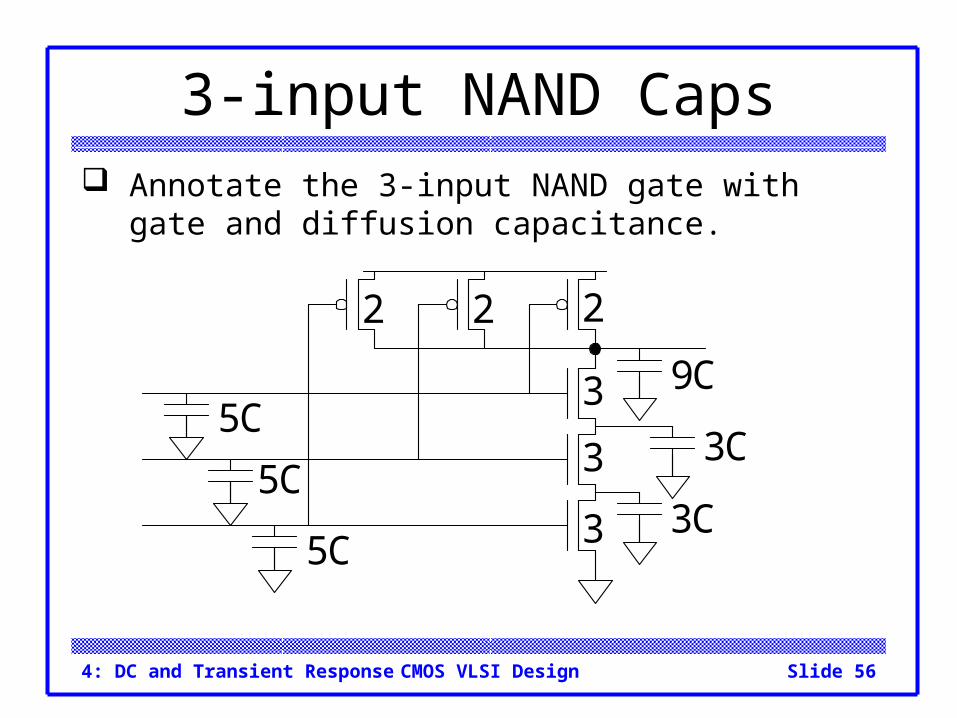
3-input NAND Caps Annotate the 3-input NAND gate with gate and
diffusion capacitance.
9C
3C
3C3
3
3
222
5C
5C
5C
4: DC and Transient Response Slide 57CMOS VLSI Design
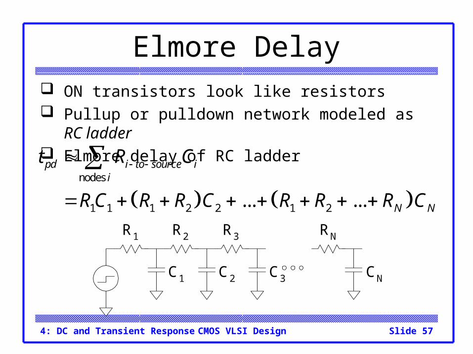
Elmore Delay ON transistors look like resistors Pullup or pulldown network modeled as RC ladder Elmore delay of RC ladder
R1 R2 R3 RN
C1 C2 C3 CN
nodes
1 1 1 2 2 1 2... ...
pd i to source ii
N N
t R C
RC R R C R R R C
4: DC and Transient Response Slide 58CMOS VLSI Design
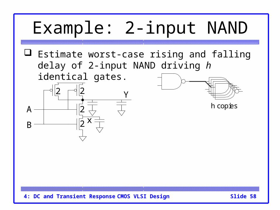
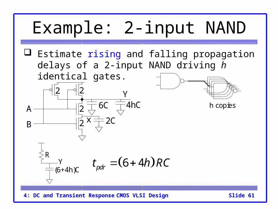
Example: 2-input NAND Estimate worst-case rising and falling delay of 2-
input NAND driving h identical gates.
h copies
2
2
22
B
Ax
Y
4: DC and Transient Response Slide 59CMOS VLSI Design
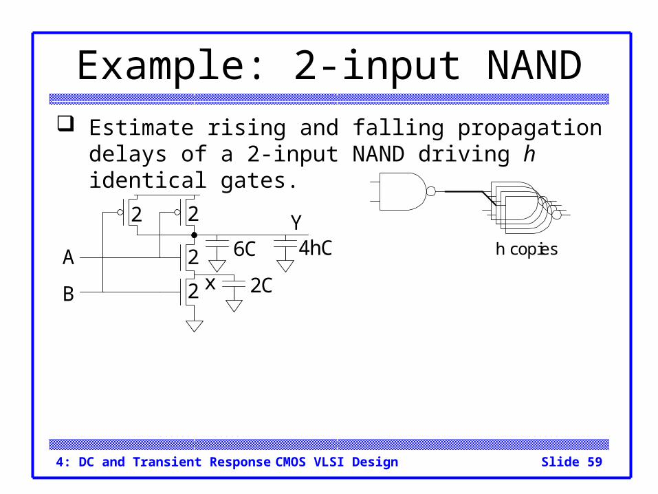
Example: 2-input NAND Estimate rising and falling propagation delays of a 2-
input NAND driving h identical gates.
h copies6C
2C2
2
22
4hC
B
Ax
Y
4: DC and Transient Response Slide 60CMOS VLSI Design
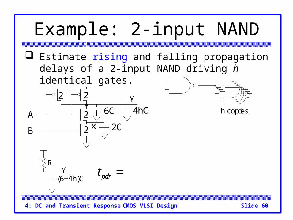
Example: 2-input NAND Estimate rising and falling propagation delays of a 2-
input NAND driving h identical gates.
h copies6C
2C2
2
22
4hC
B
Ax
Y
R
(6+4h)CY
pdrt
4: DC and Transient Response Slide 61CMOS VLSI Design
Example: 2-input NAND Estimate rising and falling propagation delays of a 2-
input NAND driving h identical gates.
h copies6C
2C2
2
22
4hC
B
Ax
Y
R
(6+4h)CY 6 4pdrt h RC
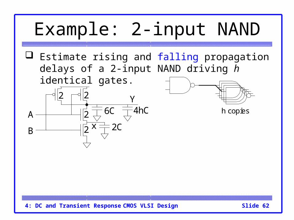
4: DC and Transient Response Slide 62CMOS VLSI Design
Example: 2-input NAND Estimate rising and falling propagation delays of a 2-
input NAND driving h identical gates.
h copies6C
2C2
2
22
4hC
B
Ax
Y
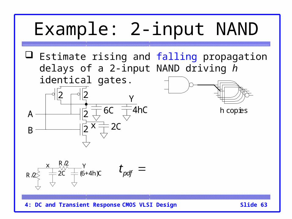
4: DC and Transient Response Slide 63CMOS VLSI Design
Example: 2-input NAND Estimate rising and falling propagation delays of a 2-
input NAND driving h identical gates.
h copies6C
2C2
2
22
4hC
B
Ax
Y
pdft (6+4h)C2CR/2
R/2x Y

4: DC and Transient Response Slide 64CMOS VLSI Design
Example: 2-input NAND Estimate rising and falling propagation delays of a 2-
input NAND driving h identical gates.
h copies6C
2C2
2
22
4hC
B
Ax
Y
2 2 22 6 4
7 4
R R Rpdft C h C
h RC
(6+4h)C2CR/2
R/2x Y
4: DC and Transient Response Slide 65CMOS VLSI Design
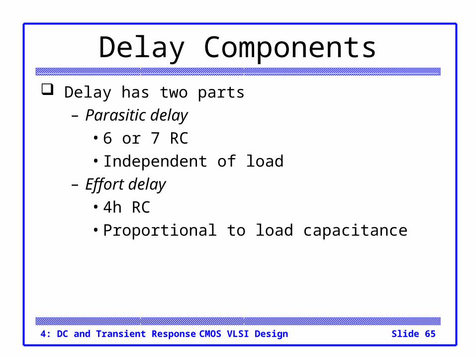
Delay Components Delay has two parts
– Parasitic delay• 6 or 7 RC• Independent of load
– Effort delay• 4h RC• Proportional to load capacitance
4: DC and Transient Response Slide 66CMOS VLSI Design
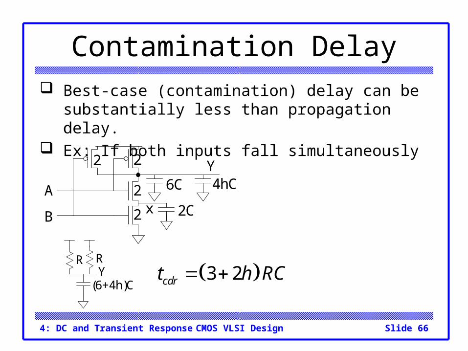
Contamination Delay Best-case (contamination) delay can be substantially
less than propagation delay. Ex: If both inputs fall simultaneously
6C
2C2
2
22
4hC
B
Ax
Y
R
(6+4h)CYR
3 2cdrt h RC
4: DC and Transient Response Slide 67CMOS VLSI Design
7C
3C
3C3
3
3
222
3C
2C2C
3C3C
IsolatedContactedDiffusionMerged
UncontactedDiffusion
SharedContactedDiffusion
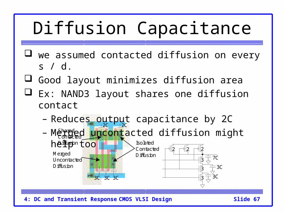
Diffusion Capacitance we assumed contacted diffusion on every s / d. Good layout minimizes diffusion area Ex: NAND3 layout shares one diffusion contact
– Reduces output capacitance by 2C– Merged uncontacted diffusion might help too
4: DC and Transient Response Slide 68CMOS VLSI Design
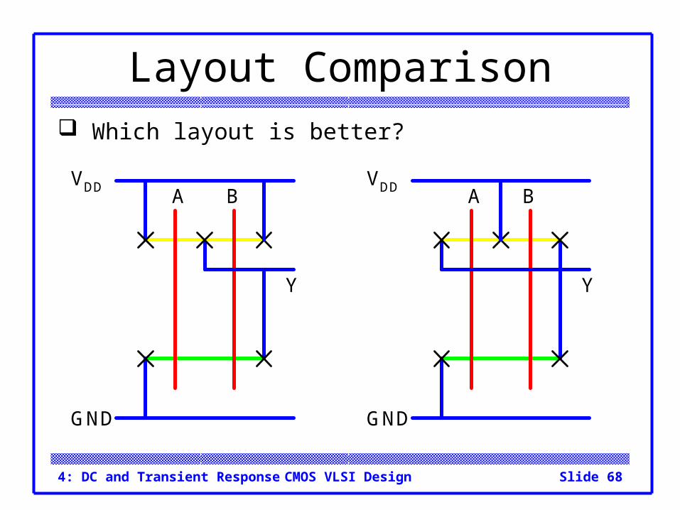
Layout Comparison Which layout is better?
AVDD
GND
B
Y
AVDD
GND
B
Y