Embed Size (px)
Citation preview
Design and FPGA Implementation
of a SISO and a MIMO Wireless System
for Software Defined Radio
Peng Dong
A Thesis
In
The Department
of
Electrical and Computer Engineering
Presented in Partial Fulfillment of the Requirements For the Degree of Master of Applied Science at
Concordia University Montreal, Quebec, Canada
March 2009
© Peng Dong, 2009
1*1 Library and Archives Canada
Published Heritage Branch
395 Wellington Street OttawaONK1A0N4 Canada
Bibliotheque et Archives Canada
Direction du Patrimoine de I'edition
395, rue Wellington Ottawa ON K1A 0N4 Canada
Your file Votre reference ISBN: 978-0-494-63333-5 Our file Notre reference ISBN: 978-0-494-63333-5
NOTICE: AVIS:
The author has granted a nonexclusive license allowing Library and Archives Canada to reproduce, publish, archive, preserve, conserve, communicate to the public by telecommunication or on the Internet, loan, distribute and sell theses worldwide, for commercial or noncommercial purposes, in microform, paper, electronic and/or any other formats.
L'auteur a accorde une licence non exclusive permettant a la Bibliotheque et Archives Canada de reproduire, publier, archiver, sauvegarder, conserver, transmettre au public par telecommunication ou par Nnternet, prefer, distribuer et vendre des theses partout dans le monde, a des fins commerciales ou autres, sur support microforme, papier, electronique et/ou autres formats.
The author retains copyright ownership and moral rights in this thesis. Neither the thesis nor substantial extracts from it may be printed or otherwise reproduced without the author's permission.
L'auteur conserve la propriete du droit d'auteur et des droits moraux qui protege cette these. Ni la these ni des extraits substantiels de celle-ci ne doivent etre imprimes ou autrement reproduits sans son autorisation.
In compliance with the Canadian Privacy Act some supporting forms may have been removed from this thesis.
Conformement a la loi canadienne sur la protection de la vie privee, quelques formulaires secondaires ont ete enleves de cette these.
While these forms may be included in the document page count, their removal does not represent any loss of content from the thesis.
Bien que ces formulaires aient inclus dans la pagination, il n'y aura aucun contenu manquant.
1+1
Canada
ABSTRACT
Design and FPGA Implementation
of a SISO and a MIMO Wireless System
for Software Defined Radio
Peng Dong
MIMO (Multiple-input Multiple-output) technology combined with space time coding techniques
provides significant increase in performance and capacity over an equivalent SISO (Single-input
Single-output) system while maintaining the same bandwidth and transmission power. MIMO has
emerged as the major breakthrough in recent communication technologies. To migrate from SISO
to MIMO system, multiple RF (Radio Frequency) front ends and additional signal processing are
required. Software defined radio (SDR) allows MIMO and other evolving techniques to be added
to current systems through software update instead of hardware replacement. SDR provides a
flexible and economic solution to the system upgrade and migration.
In this thesis, an SDR based SISO system using QPSK modulation scheme is implemented
on FPGA. The system produces signal with an intermediate frequency of 25 MHz and throughput
of 12.5 Mbps. One carrier recovery and two symbol timing recovery algorithms (Gardner and
Maximum Likelihood) are investigated and implemented. A 2x1 MIMO system using Alamouti
scheme and CORDIC based carrier recovery is designed as well. The SDR based SISO system
can be easily incorporated to the MIMO design. Throughout this thesis, detailed design
information is presented along with both computer simulation results and real hardware
performance. The comparisons of different algorithms and component structures are also
provided. Based on these comparisons, the suitable algorithm or structure according to specific
implementation considerations and system requirement can be selected.
The design and implementation are processed based on a system-level design flow. System
modeling and simulation are performed using Xilinx's System Generator for DSP and Simulink.
iii
After it is mapped to HDL (Hardware Description Language) netlist, the design is synthesized
and implemented by Xilinx's ISE tool. The generated bit-stream is then downloaded to target
FPGA to program the device. The hardware performance is measured by BER (Bit Error Rate)
tester, oscilloscope and spectrum analyzer.
This thesis is an initial project for future work of Wireless Design Laboratory at Concordia
University. The system realized in this project can be viewed as a base of future MTMO
implementation with different number of antennas and advanced signal processing techniques.
IV

Acknowledgements
I would like to take this opportunity to express my sincere appreciation to my supervisor, Dr.
Yousef R. Shayan who motivated me in working on this implementation-oriented thesis and also
lead me to the path of practical design of wireless system. His direction and support are critical in
developing this thesis. He has been a constant source of inspiration, and has provided consistent
succors and valuable suggestions throughout this project. Without these help he provided, this
work would not have been possible.
Besides, I am particularly grateful to the manager of Wireless Design Lab, Mr. Nick Ierfino.
As an expert in radio and embedded system design, he shared the precious experience with me.
He also offered helpful assistance during the hardware test of this project. It was a pleasant time
to work with him.
I owe the deepest gratitude to my beloved parents. Their continuous encouragement and
support make it possible for me to pursue a successful study and happy life in Montreal.
Last but never least, I would like to thank my colleagues in the lab and Miss Xuan Liu for
their individual support.
v
Table of Contents
List of Figures ix
List of Tables xiii
List of Acronyms xiv
Chapter 1 Introduction 1
1.1 Background 1
1.2 Motivation and Contribution of the Thesis 3
1.3 Methodology of Design and Implementation 5
1.4 Thesis Organization 7
Chapter 2 Design and Implementation of a SISO System 9
2.1 A Typical Digital Communication System 9
2.2 Overview of a SISO System Design 11
2.3 Baseband QPSK Modulator 12
2.3.1 Background 12
2.3.2 Design and Implementation 14
2.4 Pulse Shaping Filter and Interpolation Filter 14
2.4.1 Pulse Shaping Filter 14
2.4.2 Interpolation Filter 18
2.5 Digital Up and Down Conversion 22
2.5.1 Background 22
2.5.2 Design and Implementation 24
2.6 Decimation Filter and Matched Filter 27
vi
2.6.1 Background 27
2.6.2 Design and Implementation 28
2.7 Baseband QPSK Demodulation 31
Chapter 3 Synchronization for SISO System 33
3.1 Carrier Recovery 34
3.1.1 Background 34
3.1.2 Design and Implementation of CR Loop 36
3.1.3 Simulation and Analysis 43
3.2 Symbol Timing Recovery 46
3.2.1 Background 46
3.2.2 Main Components in STR loop 50
3.2.3 Design and Implementation of STR Loop 55
3.2.4 Simulation and Analysis 59
Chapter 4 Design and Implementation of a MIMO System 65
4.1 Overview of a MIMO System Design 66
4.2 Alamouti Encoding and ML Decoding 67
4.2.1 Introduction of Multipath Fading Channel 67
4.2.2 Introduction of Alamouti Scheme 69
4.2.3 Design and Implementation 70
4.3 Carrier Recovery for MIMO System 73
4.3.1 Background 73
4.3.2 Design and Implementation 75
4.3.3 Simulation and Analysis 79
vii
Chapter 5 Hardware Description and Test Results 83
5.1 Introduction of Test Equipment 83
5.1.1 XtremeDSP Board 83
5.1.2 FB100ABER Tester 85
5.2 Hardware Setup and Connection 86
5.3 Hardware Test Results 87
5.3.1 Signal Observation in Time and Frequency Domain 88
5.3.2 Signal Observation Using Constellation Plot 90
5.3.3 BER Performance 91
5.3.4 Hardware Utilization 93
5.3.5 Work Station Overview 95
Chapter 6 Conclusion and Future Work 97
6.1 Conclusion and Summary of the Thesis 97
6.2 Future Work 98
Bibliography 100
Vlll
List of Figures
Figure 1-1 Digital signal processing in SDR based receiver 2
Figure 1 -2 Design and implementation flow, and related software and hardware 7
Figure 2-1 Basic components of a digital communication system 10
Figure 2-2 Block diagram of proposed SISO system design® IF of 25 MHz 11
Figure 2-3 QPSK constellation 13
Figure 2-4 Theoretical BER performance of QPSK over AWGN channel 13
Figure 2-5 Baseband QPSK modulator 14
Figure 2-6 Impulse (a) and frequency (b) response of a SQRC filter with different roll-off
factors 16
Figure 2-7 Impulse (a) and magnitude (b) response of a 32-tap pulse shaping filter 17
Figure 2-8 Impulse (a) and magnitude (b) response of a 64-tap interpolation filter 17
Figure 2-9 Upsampled signal spectrum and interpolation filter 18
Figure 2-10 Polyphase partition for interpolation filter when L = 4 20
Figure 2-11 Parallel structure for polyphase interpolation filter 21
Figure 2-12 Digital up and down conversion 23
Figure 2-13 Phase to amplitude conversion in DDS 25
Figure 2-14 DDS block diagram 26
Figure 2-15 Downsampled signal spectrum and decimation filter 27
Figure 2-16 Polyphase partition for Decimation filter when M = 4 29
Figure 2-17 Parallel structure for polyphase decimation filter 31
Figure 2-18 QPSK baseband demodulator 32
Figure 3-1 Effect of phase (a) and frequency (b) offset on the QPSK signal constellation 35
ix
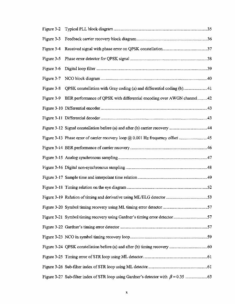
Figure 3-2 Typical PLL block diagram 35
Figure 3-3 Feedback carrier recovery block diagram 36
Figure 3-4 Received signal with phase error on QPSK constellation 37
Figure 3-5 Phase error detector for QPSK signal 38
Figure 3-6 Digital loop filter 39
Figure 3-7 NCO block diagram 40
Figure 3-8 QPSK constellation with Gray coding (a) and differential coding (b) 41
Figure 3-9 BER performance of QPSK with differential encoding over AWGN channel 42
Figure 3-10 Differential encoder 43
Figure 3-11 Differential decoder 43
Figure 3-12 Signal constellation before (a) and after (b) carrier recovery 44
Figure 3-13 Phase error of carrier recovery loop @ 0.001 Hz frequency offset 45
Figure 3-14 BER performance of carrier recovery 46
Figure 3-15 Analog synchronous sampling 47
Figure 3-16 Digital non-synchronous sampling 48
Figure 3-17 Sample time and interpolant time relation 49
Figure 3-18 Timing relation on the eye diagram 52
Figure 3-19 Relation of timing and derivative using ML/ELG detector 53
Figure 3-20 Symbol timing recovery using ML timing error detector 57
Figure 3-21 Symbol timing recovery using Gardner's timing error detector 57
Figure 3-22 Gardner's timing error detector 57
Figure 3-23 NCO in symbol timing recovery loop 59
Figure 3-24 QPSK constellation before (a) and after (b) timing recovery 60
Figure 3-25 Timing error of STR loop using ML detector 61
Figure 3-26 Sub-filter index of STR loop using ML detector 61
Figure 3-27 Sub-filter index of STR loop using Gardner's detector with f3 = 0.35 63
x
Figure 3-28 Sub-filter index of STR loop using Gardner's detector with /? = 0.7 63
Figure 3-29 BER performance of STR using ML detector 64
Figure 3-30 BER comparison between ML detector and Gardner's detector 64
Figure 4-1 Block diagram of proposed MEMO system design 67
Figure 4-2 Alamouti encoding and ML decoding in a 2x1 MIMO system 69
Figure 4-3 Alamouti encoder 71
Figure 4-4 ML decoder 72
Figure 4-5 Alamouti encoded QPSK signal constellation 73
Figure 4-6 Received signal constellation with phase offset 75
Figure 4-7 Signal mapper in carrier recovery 76
Figure 4-8 Quadrant mapper (step 1) in CORDIC algorithm 77
Figure 4-9 i'h iteration stage (step 2) in CORDIC algorithm 78
Figure 4-10 Quadrant de-mapper (step 3) CORDIC algorithm 78
Figure 4-11 BER performance of Alamouti scheme over AWGN and flat fading channel 80
Figure 4-12 Signal constellation before (a) and after (b) carrier recovery 80
Figure 4-13 Phase error of MIMO carrier recovery loop @ 0.001 Hz frequency offset 81
Figure 4-14 BER performance of CORDIC based carrier recovery 82
Figure 5-1 Hardware connection and signal routing path 87
Figure 5-2 Modulated QPSK signal in time domain @ 25 MHz 88
Figure 5-3 Signal spectrum centered @ 25 MHz 89
Figure 5-4 Spectrum showing the first image @ 175 MHz 89
Figure 5-5 Source bits (upper) and detected bits (lower) 90
Figure 5-6 Signal constellation before (a) and after (b) carrier recovery 91
Figure 5-7 BER comparison between software simulation and hardware test (Carrier recovery)
92
XI
Figure 5-8 BER comparison between software simulation and hardware test (Carrier and timing
recovery) 92
Figure 5-9 Virtex-4 FPGA overview 93
Figure 5-10 Workstation Overview 96
Figure 5-11 XtremeDSP board (a) and BER tester (b) 96
Xll
List of Tables
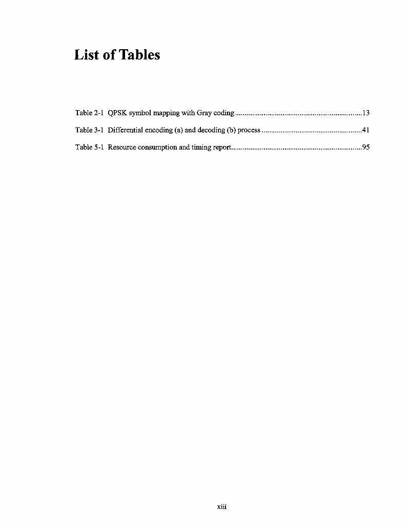
Table 2-1 QPSK symbol mapping with Gray coding 13
Table 3-1 Differential encoding (a) and decoding (b) process 41
Table 5-1 Resource consumption and timing report 95
xui
List of Acronyms
Acronym
ADC
ASICs
ASSPs
BER
BPSK
CDMA
CORDIC
CR
DAC
DDC
DSP
DSPs
DUC
DVB-S
FDM
FPGA
IF
IIR
ISI
LSTC
LTE
LUT
Expansion
Analog to Digital Convertor
Application Specific Integrated Circuits
Application Specific Standard Parts
Bit Error Rate
Binary Phase Shift Keying
Code Division Multiple Access
Coordinate Rotation Digital Computer
Carrier Recovery
Digital to Analog Convertor
Digital Down-Convertor
Digital Signal Processing
Digital Signal Processors
Digital Up-Convertor
Digital Video Broadcasting Satellite
Frequency Division Multiplexing
Field Programmable Gate Array
Intermediate frequency
Infinite Impulse Response
Inter-Symbol Interference
Layered Space-Time Codes
Long Term Evolution
Look-Up Table
MAC
Mbaud
M M O
ML
Msps
NCO
OFDM
PSC
PSF
PSK
QAM
QPSK
QoS
ROM
SDR
SISO
SNR
SPC
SQRC
STBC
STC
STR
STTC
VCO
VHDL
Multiply-and-Accumulate
Mega-Symbol per Second
Multiple-Input Multiple-Output
Maximum Likelihood
Mega-Sample per Second
Numerical-Controlled-Oscillator
Orthogonal Frequency Division Multiplexing
Probability Density Function
Parallel to Serial Convertor
Pulse Shaping Filter
Phase-Shift Keying
Quadrature Amplitude Modulation
Quadrature Phase Shift Keying
Quality of Service
Read Only Memory
Software Defined Radio
Single-Input Single-Output
Signal to Noise Ratio
Serial to Parallel Convertor
Square Root Raised Cosine
Space-Time Block Codes
Space Time Coding
Symbol Timing Recovery
Space-Time Trellis Codes
Voltage-Controlled-Oscillator
Very-High-Speed Integrated Circuits or VHSIC HDL
Chapter 1
Introduction
1.1 Background
With the ever increasing demand of wireless and mobile communication, a system that can
provide high rate data, voice, image, video and other multimedia capabilities is highly required.
As a major breakthrough in recent communications technologies, Multiple-input Multiple-output
(MIMO) technology provides significant increase in system capacity and performance by means
of using multiple antennas at transmitter and/or receiver and space time coding technique. Much
higher data rate, better Quality of Service (QoS) and enhanced transmission reliability can be
achieved in a MIMO system compared with the traditional Single-input Single-output (SISO)
system. MIMO has attracted great interest from academia to industry for the last decade, and has
become the foundation for next-generation wireless communication systems.
However, these benefits are obtained at the expense of multiple RF (Radio Frequency) front-
ends and additional signal processing required for space time coding and decoding. To migrate
from SISO to MIMO system, traditional hardware intervention results in high costs and low
flexibility in supporting multiple waveform standards [1]. A cost effective MIMO system can be
realized by means of software defined radio (SDR) technology. Quoted from SDR forum [2], the
term SDR is defined as "Radio in which some or all of the physical layer functions are software
defined". In other words, most of the signal processing on physical layer is implemented through
1
configurable software or hardware operating on programmable processing technologies. The new
signal processing techniques, air interface protocols and functionalities can be upgraded through
software instead of a complete hardware replacement. As a result, SDR allows the MIMO and
future technology to be added in current systems via simple software update. SDR provides an
inexpensive solution of building multi-mode, multi-band and multifunctional wireless
communication devices [2]. Due to its flexibility and cost-efficiency, this technology brings
considerable benefits to product manufacturers, service providers and users. In the recent years,
SDR has been widely used in the areas of cellular system, satellite communication and defense
application.
As a requirement of SDR, digital signal processing (DSP) has become a preferred choice for
implementation of communication systems, instead of traditional analog signal processing. Thus
the sophisticated signal processing tasks, such as error control coding, synchronization,
equalization, power control, channel estimation and so on, are all performed on the SDR based
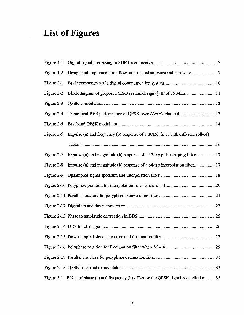
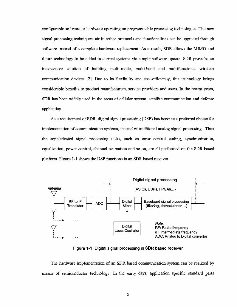
platform. Figure 1-1 shows the DSP functions in an SDR based receiver.
I signal processing •
Is, DSPs, FPGAs...) J
Baseband signal processing i t (filtering, demodulation...)
Note: RF: Radio frequency IF: Intermediate frequency ADC: Analog to Digital converter
Figure 1-1 Digital signal processing in SDR based receiver
The hardware implementation of an SDR based communication system can be realized by
means of semiconductor technology. In the early days, application specific standard parts
Antenna
Y RF to IF
Translator ADC
Digit:
(ASI
Digital Mixer
Digital Local Oscillator
2
(ASSPs), application specific integrated circuits (ASICs), digital signal processors (DSPs) and
general-purpose microcontroller were the main solutions of building an SDR platform [3]. During
the last decade, field programmable gate array (FPGA) that can offer both high performance and
flexibility has become the mainstream among these technology solutions, to meet the design
requirement for ever increasing complexity of communication systems.
FPGA is a general-purpose integrated circuit that is programmed by the designer rather than
the device manufacturer, which means it can be reprogrammed without changing any component
or interconnection at system level even after it has been deployed into a system. Compared with
traditional ASICs and DSPs, FPGA features the following advantages [3] [4]:
• High-performance and high-speed signal processing capability through parallelism
• Low risk due to the flexible architecture
• Low power consumption and cost
• Completely reconfigurable, allowing design migration for changing system protocols
• Fast time-to-market for industry purpose
In addition, with the help of embedded DSP processors and dedicated multipliers, FPGAs are
powerful and suitable for realizing DSP functions.
1.2 Motivation and Contribution of the Thesis
The objective of this thesis is to design and implement an SDR based SISO and MIMO system on
FPGA. The topic on design and implementation of communication system has been explained
broadly in literature. For example, a QAM (Quadrature Amplitude Modulation) based receiver for
SDR is implemented by C. Dick et al [5]. A DVB (Digital Video Broadcasting) receiver is
implemented on FPGA by F. Cardells et al [6][7]. The system design using Xilinx's design tool
for WCDMA and CDMA2000 base station can be found in [8][9]. The design process using
3
Altera's design tool is described in [10][11]. On the other hand, some MIMO based
implementation and testbeds were claimed [12]-[18].
Among the published work, most of them focus on the algorithm explanation and computer
simulation. Few of the work present the detailed design and real hardware performance. The key
feature of our work is implementation of an SDR based SISO wireless system on FPGA. A 2x1
MIMO system using Alamouti scheme is designed as well. The SISO system can be easily
incorporated into the MIMO design to achieve higher throughput. The specifications of the
proposed design are provided along with the real hardware performance. The major contributions
of this thesis include:
• An SDR based SISO system using QPSK (Quadrature Phase Shift Keying) modulation
scheme is successfully implemented on FPGA. The system has an IF of 25 MHz and a
throughput of 12.5 Mbps, which can be up to 15.818 Mbps.
• The specifications of the design and implementation are provided for the proposed SISO
system. This design can be used as a base of a MIMO system. Various modulation schemes
can be applied without changing most of the components including baseband signal
processing and digital up/down conversion. Carrier frequency can be configured as well to
fulfill the specific requirement.
• The parallel polyphase structure for interpolation and decimation filter, which is suitable for
high data rate, is proposed.
• One carrier recovery algorithm and two symbol timing recovery algorithms are investigated,
designed, and implemented. Their performances are also evaluated and compared using both
computer simulations and hardware test.
• A study of a 2x1 MIMO system based on Alamouti scheme is made. Detailed design for
Alamouti encoder, Maximum likelihood decoder, and carrier recovery using CORDIC
algorithm is provided. The SISO system design is flexible and easy to migrate to this MIMO
system and future designs.
4
• The real hardware performance is examined for the proposed SISO system design, and 1.2-
dB implementation loss is presented. The BER (Bit Error Rate) performance and hardware
utilization are also compared for two different timing recovery algorithms. This provides
information to readers of choosing different algorithms based on different design criterion
(performance or resources).
This thesis is an initial project for future work of Wireless Design Lab at Concordia
University. The lab was established in 2008 to improve Research and Development in areas of
digital system design, embedded microcontrollers and wireless technologies. The lab is equipped
with full set of hardware and software for design and implementation of wireless communication
systems. Numbers of industry-level testbeds are available, such as Virtex-5, Virtex-4, and Virtex-
II Pro FPGAs from Xilinx, SignalMaster Quad development platform and dual channel RF
transceiver from Lyrtech, and XtremeDSP board from Nallatech. Besides, full set of test
equipment are available as well, such as fading channel emulator, BER tester, vector signal
generator, vector analyzer, network analyzer, oscilloscope, spectrum analyzer and so forth.
Combined with Xilinx's design suit, Wireless Design Lab provides sufficient resources and ideal
solution for system design and verification.
1.3 Methodology of Design and Implementation
Traditionally, FPGA based DSP design is realized using standard register transfer level (RTL)
flow. At this level, the design is modeled as a combinational circuit separated by registers and a
set of transfer functions which describe the data flow between the registers. In addition, two
distinct sets of design tools are normally required, one for algorithm development and analysis
such as C/C++ and Matlab, and another for hardware synthesis and implementation such as
Hardware Description Language (HDL). After manually converting the high level design with
floating point representation into hardware model with fixed point representation, the design is
5
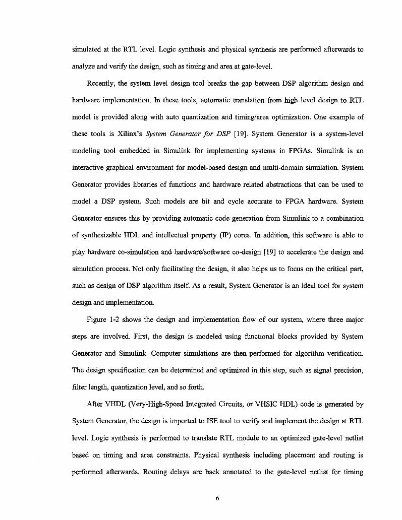
simulated at the RTL level. Logic synthesis and physical synthesis are performed afterwards to
analyze and verify the design, such as timing and area at gate-level.
Recently, the system level design tool breaks the gap between DSP algorithm design and
hardware implementation. In these tools, automatic translation from high level design to RTL
model is provided along with auto quantization and timing/area optimization. One example of
these tools is Xilinx's System Generator for DSP [19]. System Generator is a system-level
modeling tool embedded in Simulink for implementing systems in FPGAs. Simulink is an
interactive graphical environment for model-based design and multi-domain simulation. System
Generator provides libraries of functions and hardware related abstractions that can be used to
model a DSP system. Such models are bit and cycle accurate to FPGA hardware. System
Generator ensures this by providing automatic code generation from Simulink to a combination
of synthesizable HDL and intellectual property (IP) cores. In addition, this software is able to
play hardware co-simulation and hardware/software co-design [19] to accelerate the design and
simulation process. Not only facilitating the design, it also helps us to focus on the critical part,
such as design of DSP algorithm itself. As a result, System Generator is an ideal tool for system
design and implementation.
Figure 1-2 shows the design and implementation flow of our system, where three major
steps are involved. First, the design is modeled using functional blocks provided by System
Generator and Simulink. Computer simulations are then performed for algorithm verification.
The design specification can be determined and optimized in this step, such as signal precision,
filter length, quantization level, and so forth.
After VHDL (Very-High-Speed Integrated Circuits, or VHSIC HDL) code is generated by
System Generator, the design is imported to ISE tool to verify and implement the design at RTL
level. Logic synthesis is performed to translate RTL module to an optimized gate-level netlist
based on timing and area constraints. Physical synthesis including placement and routing is
performed afterwards. Routing delays are back annotated to the gate-level netlist for timing
6
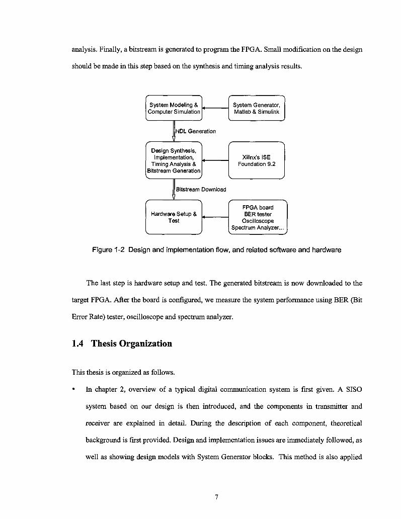
analysis. Finally, a bitstream is generated to program the FPGA. Small modification on the design
should be made in this step based on the synthesis and timing analysis results.
System Modeling & Computer Simulation
' HDL Generation
System Generator, Matlab & Simulink
Design Synthesis, Implementation,
Timing Analysis & Bitstream Generation
Xilinx's ISE Foundation 9.2
Bitstream Download
Hardware Setup & Test
FPGA board BER tester
Oscilloscope Spectrum Analyzer..
Figure 1-2 Design and implementation flow, and related software and hardware
The last step is hardware setup and test. The generated bitstream is now downloaded to the
target FPGA. After the board is configured, we measure the system performance using BER (Bit
Error Rate) tester, oscilloscope and spectrum analyzer.
1.4 Thesis Organization
This thesis is organized as follows.
• In chapter 2, overview of a typical digital communication system is first given. A SISO
system based on our design is then introduced, and the components in transmitter and
receiver are explained in detail. During the description of each component, theoretical
background is first provided. Design and implementation issues are immediately followed, as
well as showing design models with System Generator blocks. This method is also applied
7
to the further chapters. Interpolation and decimation filter design is emphasized in chapter 2,
and two filter architectures based on parallel polyphase structure are proposed.
• In chapter 3, the synchronization issues including carrier recovery and symbol timing
recovery for a SISO system are discussed. Both floating-point and fixed point simulations
are done at this stage to verify and analyze the synchronization algorithm. In symbol timing
recovery design, two algorithms are explained and implemented. Simulation results are also
presented for comparison between them.
• In chapter 4, we focus on the design and implementation of a MIMO system. An overview of
multipath fading channel is first provided. The detail design of Alamouti encoder, Maximum
likelihood decoder and carrier recovery using CORDIC algorithm are then explained.
Simulation of carrier recovery design is also performed and analyzed.
• In chapter 5, the SISO system design is fully implemented on the FPGA, and the hardware
test results including signal observation, BER performance and resource utilization are
presented and analyzed. In addition, we briefly describe the FPGA board and test equipment
we use.
• Chapter 6 concludes this thesis, and provides some recommendations for future work.
8
Chapter 2
Design and Implementation of a SISO System
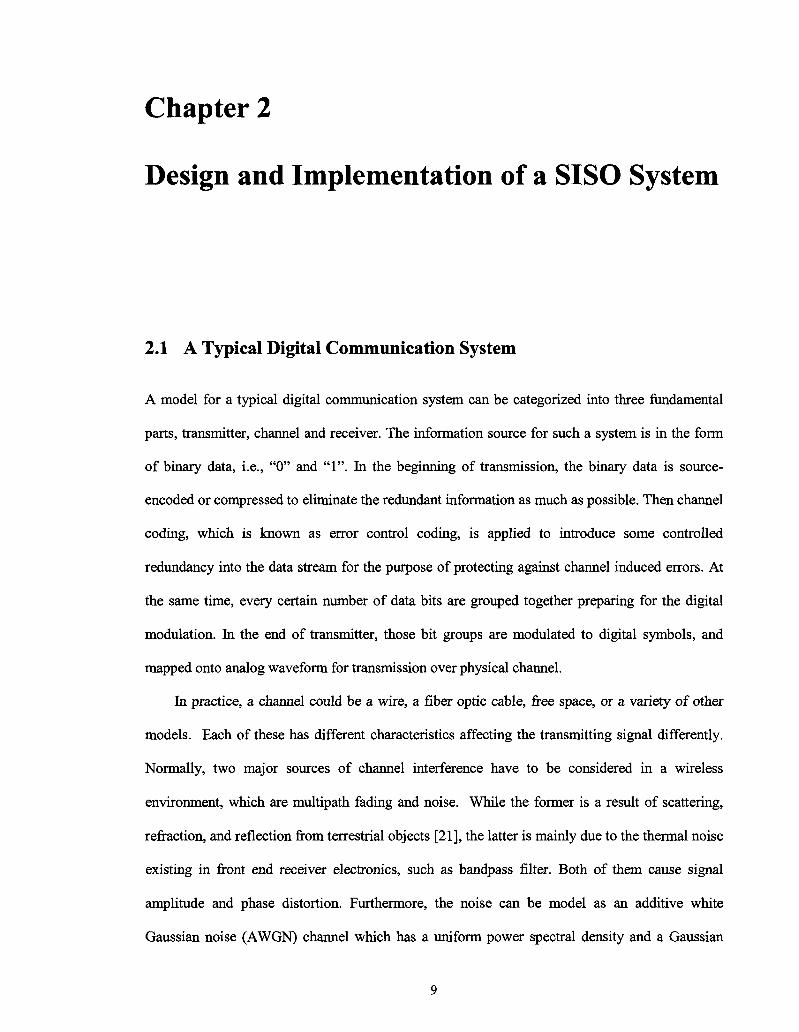
2.1 A Typical Digital Communication System
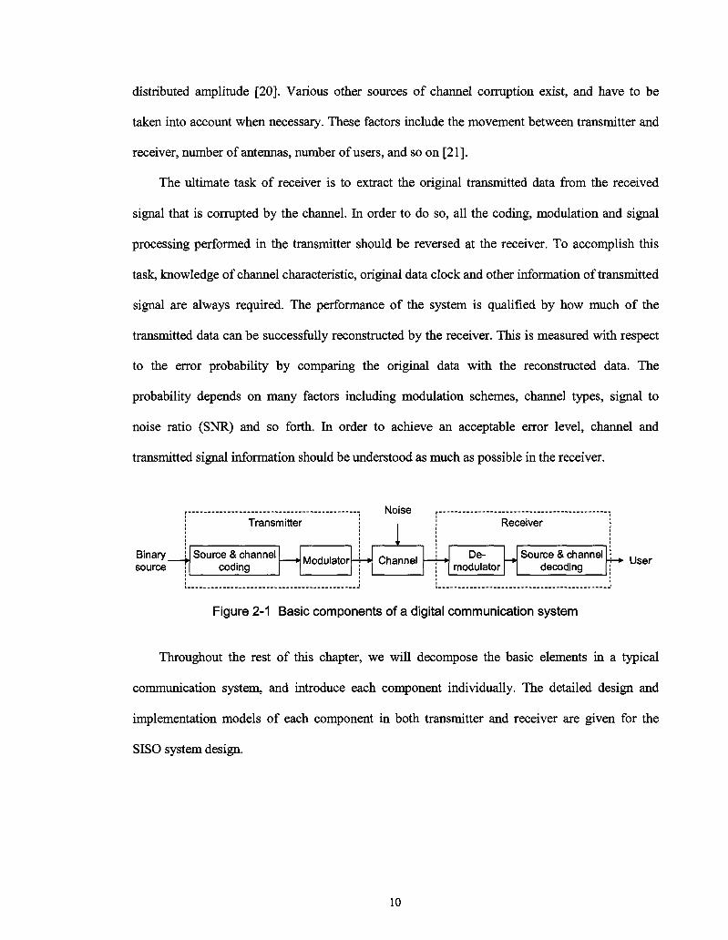
A model for a typical digital communication system can be categorized into three fundamental
parts, transmitter, channel and receiver. The information source for such a system is in the form
of binary data, i.e., "0" and " 1 " . In the beginning of transmission, the binary data is source-
encoded or compressed to eliminate the redundant information as much as possible. Then channel
coding, which is known as error control coding, is applied to introduce some controlled
redundancy into the data stream for the purpose of protecting against channel induced errors. At
the same time, every certain number of data bits are grouped together preparing for the digital
modulation. In the end of transmitter, those bit groups are modulated to digital symbols, and
mapped onto analog waveform for transmission over physical channel.
In practice, a channel could be a wire, a fiber optic cable, free space, or a variety of other
models. Each of these has different characteristics affecting the transmitting signal differently.
Normally, two major sources of channel interference have to be considered in a wireless
environment, which are multipath fading and noise. While the former is a result of scattering,
refraction, and reflection from terrestrial objects [21], the latter is mainly due to the thermal noise
existing in front end receiver electronics, such as bandpass filter. Both of them cause signal
amplitude and phase distortion. Furthermore, the noise can be model as an additive white
Gaussian noise (AWGN) channel which has a uniform power spectral density and a Gaussian
9
distributed amplitude [20]. Various other sources of channel corruption exist, and have to be
taken into account when necessary. These factors include the movement between transmitter and
receiver, number of antennas, number of users, and so on [21].
The ultimate task of receiver is to extract the original transmitted data from the received
signal that is corrupted by the channel. In order to do so, all the coding, modulation and signal
processing performed in the transmitter should be reversed at the receiver. To accomplish this
task, knowledge of channel characteristic, original data clock and other information of transmitted
signal are always required. The performance of the system is qualified by how much of the
transmitted data can be successfully reconstructed by the receiver. This is measured with respect
to the error probability by comparing the original data with the reconstructed data. The
probability depends on many factors including modulation schemes, channel types, signal to
noise ratio (SNR) and so forth. In order to achieve an acceptable error level, channel and
transmitted signal information should be understood as much as possible in the receiver.
Binary ! source [
Transmitte
Source & channel coding
— • Modulator - *
1 Channel
Receiver
Demodulator
Source & channel _ decoding User
Figure 2-1 Basic components of a digital communication system
Throughout the rest of this chapter, we will decompose the basic elements in a typical
communication system, and introduce each component individually. The detailed design and
implementation models of each component in both transmitter and receiver are given for the
SISO system design.
10
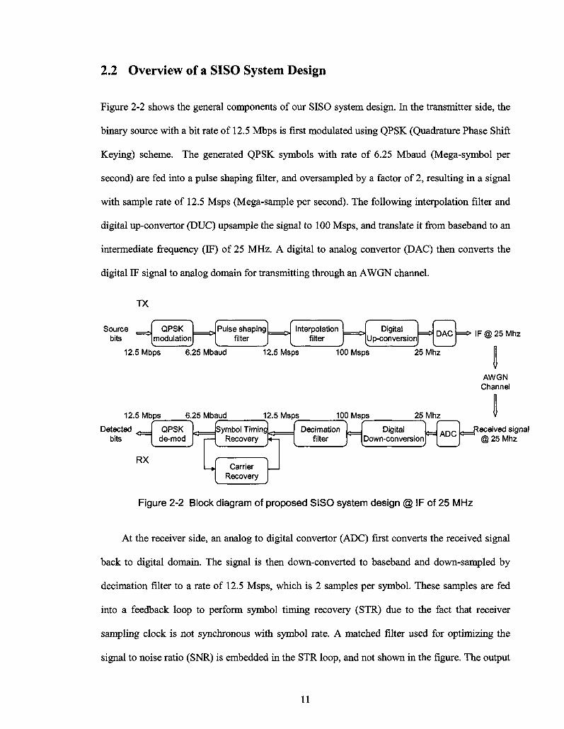
2.2 Overview of a SISO System Design
Figure 2-2 shows the general components of our SISO system design. In the transmitter side, the
binary source with a bit rate of 12.5 Mbps is first modulated using QPSK (Quadrature Phase Shift
Keying) scheme. The generated QPSK symbols with rate of 6.25 Mbaud (Mega-symbol per
second) are fed into a pulse shaping filter, and oversampled by a factor of 2, resulting in a signal
with sample rate of 12.5 Msps (Mega-sample per second). The following interpolation filter and
digital up-convertor (DUC) upsample the signal to 100 Msps, and translate it from baseband to an
intermediate frequency (IF) of 25 MHz. A digital to analog converter (DAC) then converts the
digital IF signal to analog domain for transmitting through an AWGN channel.
TX
Source bits
QPSK modulation
Pulse shaping filter
Interpolation filter
.1 "1 Digital
Up-con version DAC
12.5 Mbps 6.25 Mbaud 12.5 Msps 100 Msps 25Mhz
IF@25Mhz
AWGN Channel
12.5 Mbps 6.25 Mbaud 12.5 Msps 100 Msps 25Mhz
Detected <__ bits
QPSK de-mod
RX
Symbol Timinq Recovery
-Carrier
Recovery
Decimation filter
«= Digital Down-conversion
, n r I. Received signal A D C | ^ @25Mhz
Figure 2-2 Block diagram of proposed SISO system design @ IF of 25 MHz
At the receiver side, an analog to digital convertor (ADC) first converts the received signal
back to digital domain. The signal is then down-converted to baseband and down-sampled by
decimation filter to a rate of 12.5 Msps, which is 2 samples per symbol. These samples are fed
into a feedback loop to perform symbol timing recovery (STR) due to the fact that receiver
sampling clock is not synchronous with symbol rate. A matched filter used for optimizing the
signal to noise ratio (SNR) is embedded in the STR loop, and not shown in the figure. The output
11
of STR loop is fed into carrier recovery (CR) loop to compensate the residue carrier frequency
and phase offset. In the end, QPSK de-modulator detects the recovered symbols, and maps them
back to bits based on the QPSK mapping scheme. The bit error rate (BER) performance then can
be measured by comparing the reconstructed bits with original source bits.
Synchronization including symbol timing and carrier recovery is one of the most challenging
tasks in the system design. In this chapter, we focus on the design and implementation with
perfect timing and carrier matching between transmitter and receiver. Synchronization and
relative design issue will be introduced and discussed in detail in the next chapter.
2.3 Baseband QPSK Modulator
2.3.1 Background
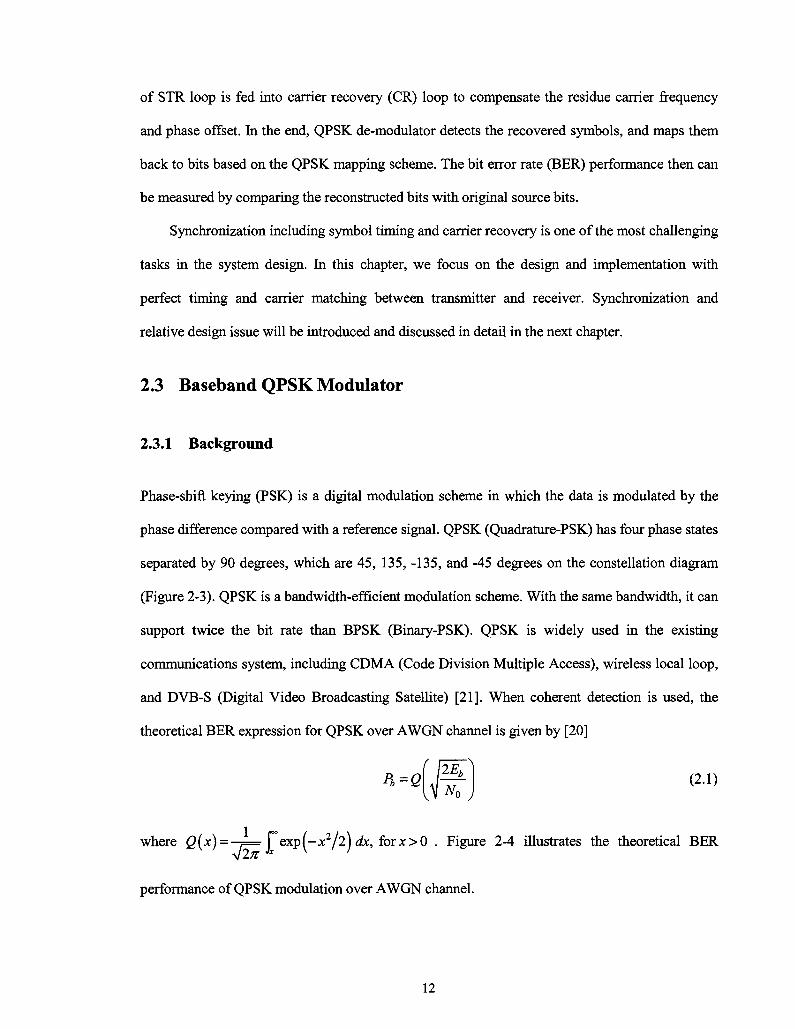
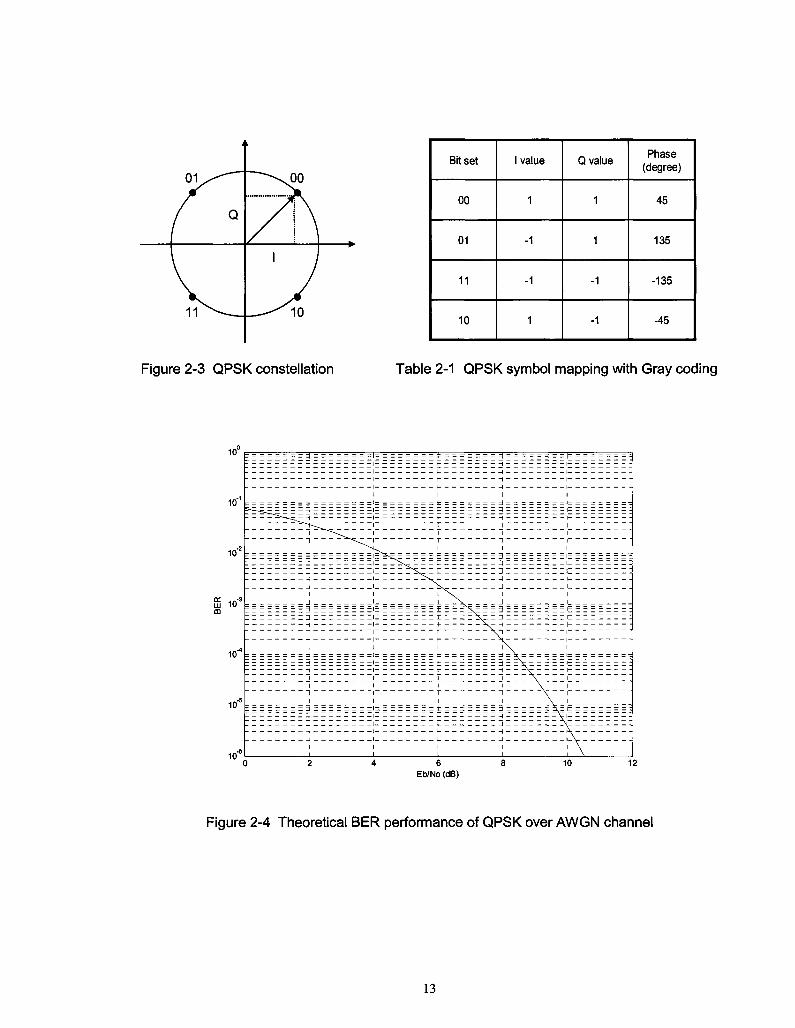
Phase-shift keying (PSK) is a digital modulation scheme in which the data is modulated by the
phase difference compared with a reference signal. QPSK (Quadrature-PSK) has four phase states
separated by 90 degrees, which are 45, 135, -135, and -45 degrees on the constellation diagram
(Figure 2-3). QPSK is a bandwidth-efficient modulation scheme. With the same bandwidth, it can
support twice the bit rate than BPSK (Binary-PSK). QPSK is widely used in the existing
communications system, including CDMA (Code Division Multiple Access), wireless local loop,
and DVB-S (Digital Video Broadcasting Satellite) [21]. When coherent detection is used, the
theoretical BER expression for QPSK over AWGN channel is given by [20]
fl=fi(JFI (zi)
where Q[x) = —j= fexp(-;c2 /2j dx, forx>0 . Figure 2-4 illustrates the theoretical BER
performance of QPSK modulation over AWGN channel.
12
Bit set
00
01
11
10
I value
1
-1
-1
1
Q value
1
1
-1
-1
Phase (degree)
45
135
-135
-45
Figure 2-3 QPSK constellation Table 2-1 QPSK symbol mapping with Gray coding
10
10
1 0 ;
ffi 10"3
CD
10
10'
10
4I-
U
1lt1
MM
1 1 4 - 1 1
1 1 1 1 1
^ ^ " k ^ i r - n i
! III!
I 1 1
MM
1 1 1
MM
1 1 1
MM
1 1
1 lilt 1 1
1
MM
1 1 1
llll 1 1
1 llll 1
1
-1— m
nn
1 M
M 1
1 1
llll 1 1
\ llll 1
1
\ llll 1
1
- I
rrtn r-
l llll 1 1
l
llll 1 1
l llll l 1
1
llll l 1
l llll 1 1
1 1 - ^ H j ' ' "
NT"
Il-I-
—iir
r 1 H \ - -1 | • i i r \ ~ i i
U -
4414-
r -
11 ir
l l l l " \ _ 1 1 1 1 ' \ '
\ 1 i 1 _ V |
j. i j - J i V i i i i i \ i i i i i \
4 6 Eb/No (dB)
10 12
Figure 2-4 Theoretical BER performance of QPSK over AWGN channel
13
2.3.2 Design and Implementation
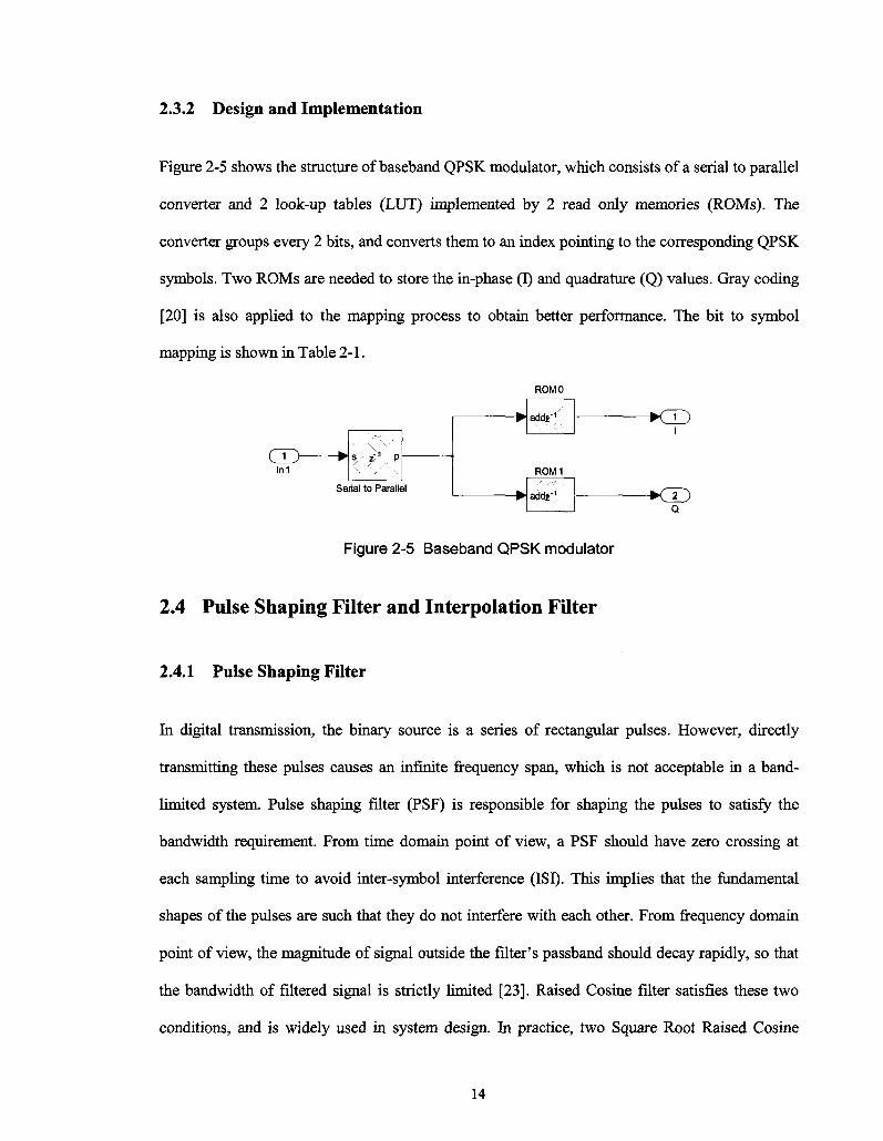
Figure 2-5 shows the structure of baseband QPSK modulator, which consists of a serial to parallel
converter and 2 look-up tables (LUT) implemented by 2 read only memories (ROMs). The
converter groups every 2 bits, and converts them to an index pointing to the corresponding QPSK
symbols. Two ROMs are needed to store the in-phase (I) and quadrature (Q) values. Gray coding
[20] is also applied to the mapping process to obtain better performance. The bit to symbol
mapping is shown in Table 2-1.
ROM0
In1 s z-
n p
Serial to Parallel
w addr1
ROM1
addr1
Figure 2-5 Baseband QPSK modulator
2.4 Pulse Shaping Filter and Interpolation Filter
2.4.1 Pulse Shaping Filter
-KX)
-KID Q
In digital transmission, the binary source is a series of rectangular pulses. However, directly
transmitting these pulses causes an infinite frequency span, which is not acceptable in a band-
limited system. Pulse shaping filter (PSF) is responsible for shaping the pulses to satisfy the
bandwidth requirement. From time domain point of view, a PSF should have zero crossing at
each sampling time to avoid inter-symbol interference (ISI). This implies that the fundamental
shapes of the pulses are such that they do not interfere with each other. From frequency domain
point of view, the magnitude of signal outside the filter's passband should decay rapidly, so that
the bandwidth of filtered signal is strictly limited [23]. Raised Cosine filter satisfies these two
conditions, and is widely used in system design. In practice, two Square Root Raised Cosine
14
(SQRC) filters are placed both in transmitter and receiver in order to have an overall raised cosine
response of the system. The SQRC filter in the transmitter is known as pulse shaping filter,
whereas the one in the receiver is called matched filter (MF). Such a combination guarantees
maximum SNR and minimum ISI for signal detection after matched filtering.
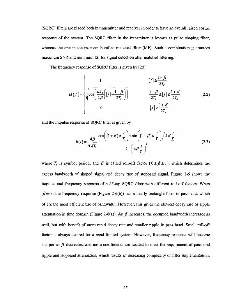
The frequency response of SQRC filter is given by [20]
1-/?
H{f) =
1 l/l*- 27;
cos (nT/
v2/*v 0
l/l-1-J3
IT. s J J 2TS ' ' 2TS
1 + fi
(2.2)
l/l 27;
and the impulse response of SQRC filter is given by
h(t) = A/3 cos (l + /3)„±) + sJ(l-P)x±) 4/3^-
' ! / nJF,
(2.3)
1 -V TsJ
where Ts is symbol period, and /? is called roll-off factor (0 < /? < 1), which determines the
excess bandwidth of shaped signal and decay rate of stopband signal. Figure 2-6 shows the
impulse and frequency response of a 65-tap SQRC filter with different roll-off factors. When
P = 0 , the frequency response (Figure 2-6(b)) has a nearly rectangle form in passband, which
offers the most efficient use of bandwidth. However, this gives the slowest decay rate or ripple
attenuation in time domain (Figure 2-6(a)). As j3 increases, the occupied bandwidth increases as
well, but with benefit of more rapid decay rate and smaller ripple in pass band. Small roll-off
factor is always desired for a band limited system. However, frequency response will become
sharper as /3 decreases, and more coefficients are needed to meet the requirement of passband
ripple and stopband attenuation, which results in increasing complexity of filter implementation.
15
In practice, a roll-off factor in range from 0.15 to 0.5 is chosen as a compromise between
bandwidth efficiency and implementation complexity.
hputse Response Magnitude Response (dB)
I t I I I -eol t L _ _ U U I I ,l III i< Jill III) '111 l M l l i l l 111 IU .A 11./ -32 -16 0 16 32 0 0.05 0.1 0.15 0.2 0.25 0.3 0.35 0.4
TOTB Normaized Frequency (xn rad/sanpte)
(a) (b)
Figure 2-6 impulse (a) and frequency (b) response of a SQRC filter with different roll-off factors
To fulfill the Nyquist sampling criterion, the filter has to operate at a rate of no less than
twice the symbol rate. Oversampling with more than two samples per symbol is desired in
practical design [24]. Since the oversampling can be accomplished by interpolation filter to be
discussed later, we simply increase the symbol rate by a factor of 2 via pulse shaping filter. The
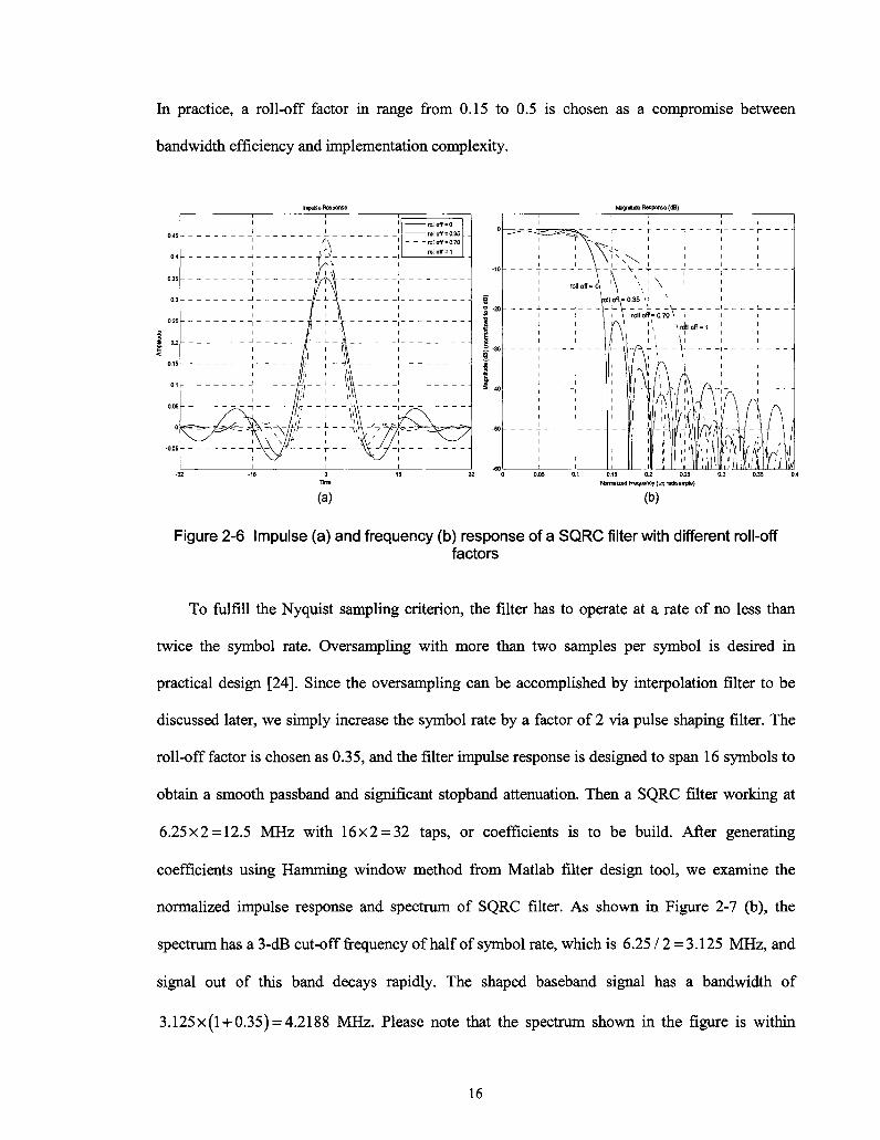
roll-off factor is chosen as 0.35, and the filter impulse response is designed to span 16 symbols to
obtain a smooth passband and significant stopband attenuation. Then a SQRC filter working at
6.25x2 = 12.5 MHz with 16x2 = 32 taps, or coefficients is to be build. After generating
coefficients using Hamming window method from Matlab filter design tool, we examine the
normalized impulse response and spectrum of SQRC filter. As shown in Figure 2-7 (b), the
spectrum has a 3-dB cut-off frequency of half of symbol rate, which is 6.25 / 2 = 3.125 MHz, and
signal out of this band decays rapidly. The shaped baseband signal has a bandwidth of
3.125x(l + 0.35) = 4.2188 MHz. Please note that the spectrum shown in the figure is within
16
single sided frequency range of [0,7^/2], where Fs is filter's sampling frequency, and the
double sided signal bandwidth is 8.4275 MHz. The architecture structure of pulse shaping filter
will be discussed after interpolation filter is introduced.
Impluse Response of 32-tap pulse shaping fil
x 1 1 6 1 1 i-
T ! ! 1J [ ! r
-L I 1 r x f ' ' L
T 1 I ~ T i ' ' r
-L I 1 / — I — \ I I i_
i ! ! 1 ! ! i i
8 12 16 20 24 28 31 Samples
(a)
Magnitude Response of 32-tap pulse shaping filter
3.125 Frequency (MHz)
(b)
Figure 2-7 Impulse (a) and magnitude (b) response of a 32-tap pulse shaping filter
Impulse response of 64-tap interpolation filter Magnitude Response of 64-tap interpolation filter
20 25 30 Frequency (MHz)
Figure 2-8 Impulse (a) and magnitude (b) response of a 64-tap interpolation filter
17
2.4.2 Interpolation Filter
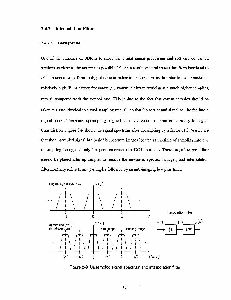
2.4.2.1 Background
One of the purposes of SDR is to move the digital signal processing and software controlled
sections as close to the antenna as possible [2]. As a result, spectral translation from baseband to
IF is intended to perform in digital domain rather in analog domain. In order to accommodate a
relatively high IF, or carrier frequency fc, system is always working at a much higher sampling
rate fs compared with the symbol rate. This is due to the fact that carrier samples should be
taken at a rate identical to signal sampling rate fs, so that the carrier and signal can be fed into a
digital mixer. Therefore, upsampling original data by a certain number is necessary for signal
transmission. Figure 2-9 shows the signal spectrum after upsampling by a factor of 2. We notice
that the upsampled signal has periodic spectrum images located at multiple of sampling rate due
to sampling theory, and only the spectrum centered at DC interests us. Therefore, a low pass filter
should be placed after up-sampler to remove the unwanted spectrum images, and interpolation
filter normally refers to an up-sampler followed by an anti-imaging low pass filter.
Original signal spectrum z(f)
Interpolation filter
z(«) x(n) y(n)
U LPF
-3/2 -1/2 o 1/2 1 3/2 f' = 2f
Figure 2-9 Upsampled signal spectrum and interpolation filter
18
2.4.2.2 Design and Implementation
When it comes to the structure of interpolation filter, polyphase partition [24] is always a good
choice. Since the upsampled signal is actually a signal with zeroes inserted between original
samples, these zeroes obviously do not contribute to the filtering process, i.e., multiplication and
addition. Let us now examine how polyphase can be applied to the interpolation design. First,
recall the digital filter transfer function
N-l
y(n) = x(n)®h{n) = Y,x{n-k)h{k) (2.4) k=0
whereh{n) is the filter's impulse response with N = S-L taps. Here, we assume that the filter
length Ncan be divided to L groups length S, where L is the upsampling factor. If x[n) is an
upsampled version of z(«) , the upsampling process can be modeled as
, x [z(n/L), if n/L is an integer c{n) = <
[ 0, otherwise (2.5)
Now, substitute k = r • L + X in Eq. (2.4), where r and X are both integers, and 0 < X < L -1.
Then we have the following expression,
L-\ 5-1
y(n) = J^x(n-(r • L + X))- h(r • L + X) (2.6) 2=0r=0
Substituting k = r • L + X in Eq. (2.5) results in
\x(n-(rxL + X)) = z(m-r), whenn = mxZ + A
[ 0, otherwise
Using both Eq. (2.6) and (2.7), we can have the expression as
£-1 5-1
y(m) = ^i^z(m-r)-h(r-L + X) Z=0r=0
L-\ 5-1 =ZZz(m - r)'Mm)
A=0 r=0
(2.8)
19
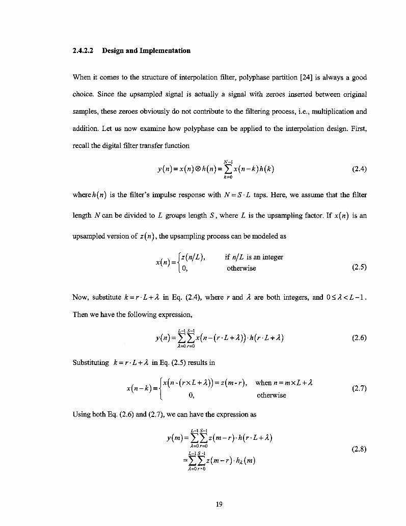
where hA(m) is actually a sub-filter deriving from original filter with a phase index X, and the
interpolation filter is successfully decomposed by polypahse structure.
Input signal-z{n)
\h{n) yo{*)
lk(n) M»J
\h{n) M")
tM") M")
^.Interpolated signal
y(n)
Figure 2-10 Polyphase partition for interpolation filter when L = 4
As shown in Figure 2-10, the polyphase structure splits the original filter into L sub-filters,
each with length of S = N/L, and impulse response of h^(n) = h(n-L + A). Specifically, the
sub-filter /TQ contains the coefficients h(L), h(2L),h(3>L),... the sub-filter hx contains the
coefficients h(L + \), h(2L + l), h(3L + l),... and so forth. These filters filter the incoming
signal in turn at upsampling rate. The results are summed up to form the interpolation output. By
doing this, no unnecessary calculation is performed, and the overall computation savings can
beN-N/L per output compared with traditional filter structure of direct-form and transpose-
form. Any design method for low pass filter can be applied to interpolation design [24]. Here, we
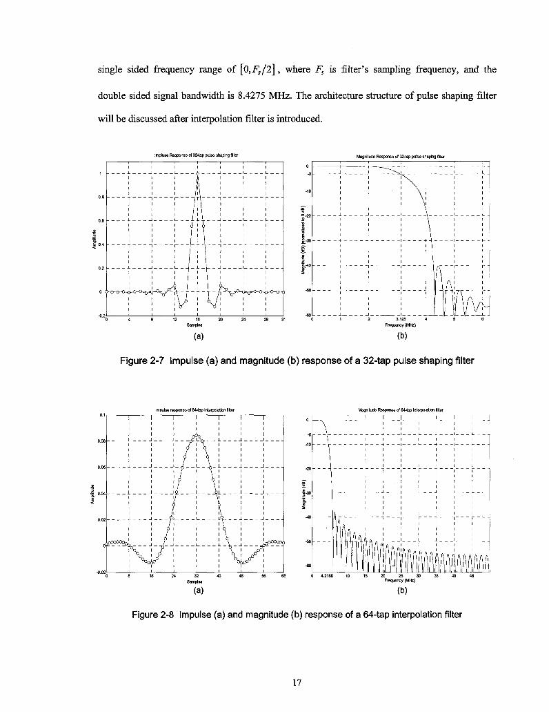
are aiming to build a 64-tap interpolation filter with sampling frequency of 12.5x8 = 100MHz
and 6-dB cut off frequency of 4.2188 MHz, which equals baseband signal bandwidth after pulse
shaping. The filter coefficients are generated using Kaiser Window method from Matlab filter
design tool. The impulse and frequency response of interpolation filter are shown in Figure 2-8.
As seen in Figure 2-8(b), the stopband attenuation is 40 dB, which also meets our requirement.
20
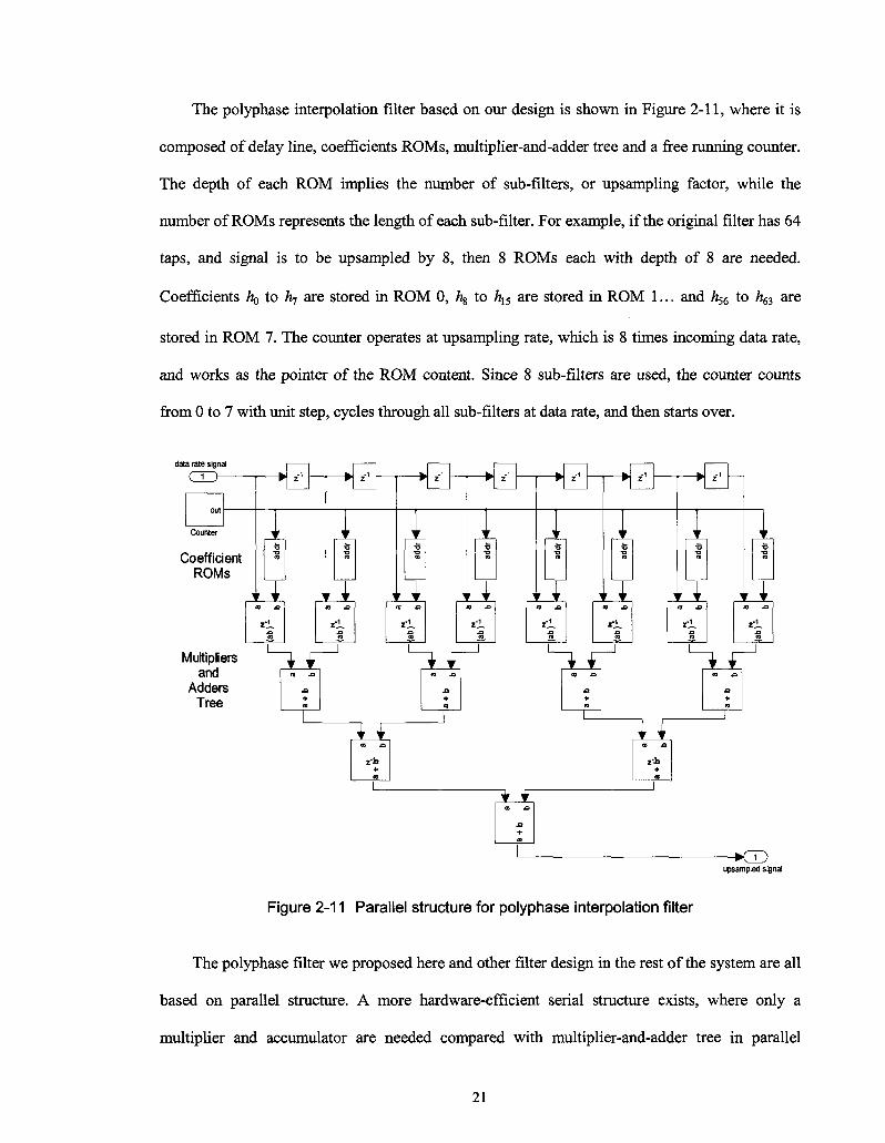
The polyphase interpolation filter based on our design is shown in Figure 2-11, where it is
composed of delay line, coefficients ROMs, multiplier-and-adder tree and a free running counter.
The depth of each ROM implies the number of sub-filters, or upsampling factor, while the
number of ROMs represents the length of each sub-filter. For example, if the original filter has 64
taps, and signal is to be upsampled by 8, then 8 ROMs each with depth of 8 are needed.
Coefficients /ZQ to hj are stored in ROM 0, /% to hX5 are stored in ROM 1... and hs6 to h6i are
stored in ROM 7. The counter operates at upsampling rate, which is 8 times incoming data rate,
and works as the pointer of the ROM content. Since 8 sub-filters are used, the counter counts
from 0 to 7 with unit step, cycles through all sub-filters at data rate, and then starts over.
data rate signal
c
v ! r
out
Counter
/oeffic ROM
ent s
<0
1 1 CO X»
x>
1
W z 1
1 1
.1 CO X I
z i XI flj
1
• z-1 -
• o • o CO
'1 CO X I
z i X I CO
1
z1
v
CO
1 CO X )
z i x>
1
z1 -
V •5 m
r v CO X I
z i XI -2.
1
z1
1 !
1 CO X I
z-1 CO
J
z 1 -
v •5
<0
CO JO
z i X I CO
1
1 -o CO
i CO JQ
z i XI
Multipliers ^ ^ and
Adders Tree
^ r L~u~J L-±TJ
* *
i j £
•XT) upsampled signal
Figure 2-11 Parallel structure for polyphase interpolation filter
The polyphase filter we proposed here and other filter design in the rest of the system are all
based on parallel structure. A more hardware-efficient serial structure exists, where only a
multiplier and accumulator are needed compared with multiplier-and-adder tree in parallel
21
structure. It is also called Multiply-and-Accumulate (MAC) operation [24][36]. However, the
processing rate of MAC depends on the filter length, that is, MAC works at 64 times data rate if
the original filter has 64 taps. Therefore, if the processing speed is limited, only very low
throughput can be tolerant when MAC filter is used. In order to transmit a relatively high rate
data, considering of the clock limitation of the platform, the parallel structure is more suitable for
our application.
The pulse shaping filter is realized by the polyphase structure as well. System Generator
provides many different filter design cores, such as filter compilers, distributed arithmetic FIR,
MAC filter and so on [19]. They can also be applied to our design. However, the use of these
existing cores normally cost more hardware utilization, which should be noticed in an area-saving
design.
2.5 Digital Up and Down Conversion
2.5.1 Background
The up conversion of baseband signal, also called spectral translation, is performed in a
communications system for two main reasons. First of all, transmission at baseband or relatively
low frequency will require extremely large antenna size and signal bandwidth [5], which is
strictly limited by device vendors. Secondly, the radio spectrum, which is at high frequency, can
be shared by multiple users through use of frequency division multiplexing (FDM) [5]. Therefore,
signal's central frequency is usually moved by an independent sinusoid carrier from DC to higher
frequency for radio transmission. In a practical radio transmitter which is shown in Figure 2-12,
the baseband I and Q signals are up-converted by mixing with a sinusoid carrier generated from a
local oscillator (LO) with phase of 0 and 90 degrees, respectively. As a result, the I and Q signals
are orthogonal and do not interfere with each other. When combined, they are summed to a
22
composite output signal. By doing so, two independent signal components are modulated onto a
single carrier wave, which can be split back into the independent components in the receiver.
Denote the baseband I and Q signal as x} (t) and xe (t), respectively. The generated carrier
wave for I and Q branches are cos(2;r/c) and -s in(2; r / c ) , respectively. Then the up-converted
signal can be expressed as
r(t) = xj {t)cos(27tfc)-xQ (r)sin(2/r/c) (2.9)
Eq. (2.9) implies that the baseband signal is modulated onto the carrier. If complex multiplication
is performed for signal xj (t) + xQ (t) j and carrier cos (2nfc) - sin {lnfc) j , only the real part of
the product is taken to form the signal for actual transmission. This process is illustrated in Figure
2-12, which also includes the down conversion in the receiver side. In practice, a frequency
translation from baseband to an IF is performed before transmission on RF. Digital up-convertor
(DUC) is such a circuit to accomplish this baseband to IF translation in digital domain, and also
to ease the rest analog circuit design.
Baseband I
cos(2^/c)
TXDDS
sin(2^/ c)
Baseband Q ,
& Channel
Noise
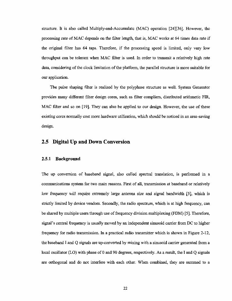
cos(^
RXDDS
• ^
-s in
^
LPF
life)
Baseband 1
{2nfc)
LPF Baseband Q
Figure 2-12 Digital up and down conversion
Before a signal is demodulated, the receiver must remove the complex envelope of the
carrier, and translate the signal spectrum from IF back to baseband for the further digital signal
processing. When this step is realized in digital domain, it is called digital down conversion
(DDC). As shown in Figure 2-12, the received signal is mixed with the reference carrier, which is
23
a coherent replica of transmitter carrier generated from local oscillator with a 90-degree phase
shift. The composite signal is thus split back into I and Q components which are independent and
orthogonal to each other. Recall that in the absence of any channel impairment the received IF
signal is given by Eq. (2.9). After down-conversion, the I (y : (t)) and Q (yQ (t)) signal can be
expressed as
yi(t) = r(t)-cos(27Tfc)
=\_xj (t)cos(2xfc)- xQ(t)sia.(27rfc)~\- cos(2xfc)
= Xj (/) + high frequency components,
yQ{t) = r{t)-sm(-2nfc)
=[xj (t)cos(27rfc) - xQ (t)sm(27tfc)] • sin (-2/r/c)
= xQ (t) + high frequency components.
Since we are only interested with the DC part, the high frequency items and other distortion can
be successfully removed by a proper low pass filter. After that, the original baseband signal is
extracted from the down-converted signal. Furthermore, in order to obtain a precise DC part, the
receiver carrier should be exactly the same as transmitter carrier, which means, same frequency
and same offset. If such a requirement is not satisfied, carrier recovery should be performed in
the receiver side, and will be discussed later.
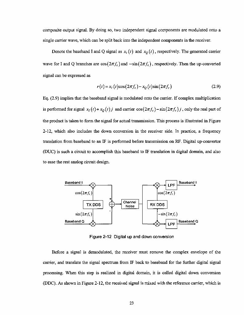
2.5.2 Design and Implementation
In digital system design, local oscillator is realized by a direct digital synthesizer (DDS), and the
DUC is composed of a DDS and a mixer. The mixer consists of 2 multipliers and a subtractor,
which corresponds to transmitter blocks in Figure 2-12. The DDS synthesizes a discrete-time
representation of a sinusoidal waveform, and can be used to generate the sinusoidal carrier with
high frequency resolution and desired spectral purity. By using DDS, the phase, frequency and
amplitude of carrier can be precisely controlled by the DSP algorithm with high speed.
24
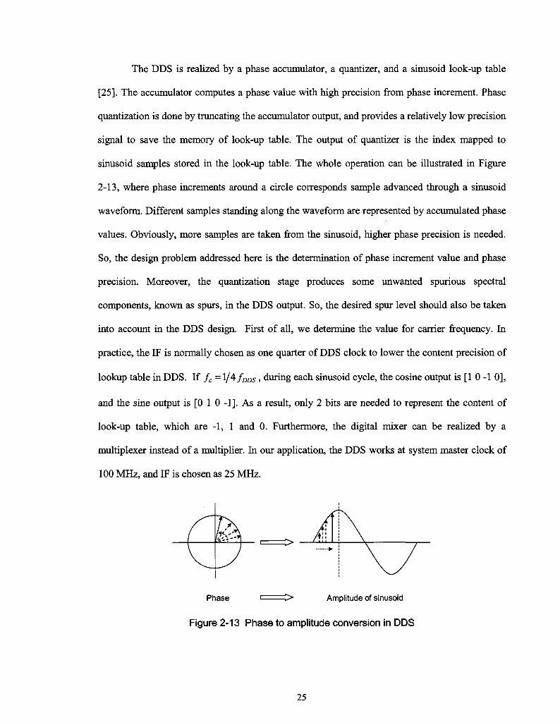
The DDS is realized by a phase accumulator, a quantizer, and a sinusoid look-up table
[25]. The accumulator computes a phase value with high precision from phase increment. Phase
quantization is done by truncating the accumulator output, and provides a relatively low precision
signal to save the memory of look-up table. The output of quantizer is the index mapped to
sinusoid samples stored in the look-up table. The whole operation can be illustrated in Figure
2-13, where phase increments around a circle corresponds sample advanced through a sinusoid
waveform. Different samples standing along the waveform are represented by accumulated phase
values. Obviously, more samples are taken from the sinusoid, higher phase precision is needed.
So, the design problem addressed here is the determination of phase increment value and phase
precision. Moreover, the quantization stage produces some unwanted spurious spectral
components, known as spurs, in the DDS output. So, the desired spur level should also be taken
into account in the DDS design. First of all, we determine the value for carrier frequency. In
practice, the IF is normally chosen as one quarter of DDS clock to lower the content precision of
lookup table in DDS. If fc = l/4fDDS, during each sinusoid cycle, the cosine output is [1 0-1 0],
and the sine output is [0 1 0 -1]. As a result, only 2 bits are needed to represent the content of
look-up table, which are -1, 1 and 0. Furthermore, the digital mixer can be realized by a
multiplexer instead of a multiplier. In our application, the DDS works at system master clock of
100 MHz, and IF is chosen as 25 MHz.
Phase ' i > Amplitude of sinusoid
Figure 2-13 Phase to amplitude conversion in DDS
25
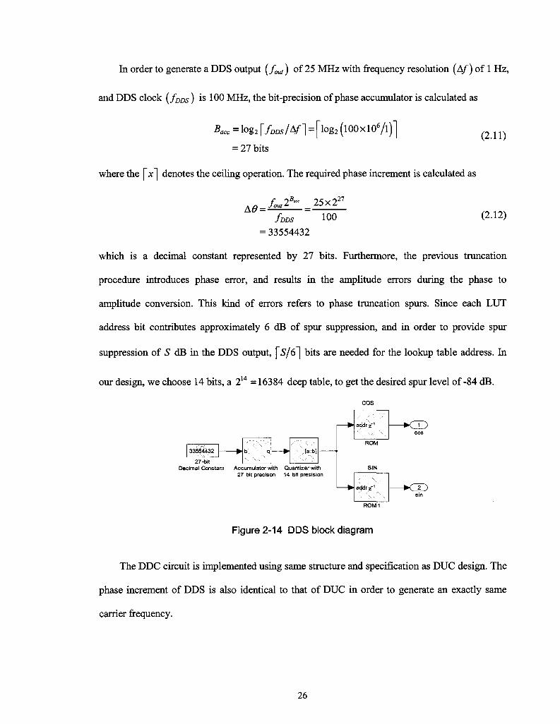
In order to generate a DDS output ( / ^ ) of 25 MHz with frequency resolution (A/-) of 1 Hz,
and DDS clock (fDDS) is 100 MHz, the bit-precision of phase accumulator is calculated as
Bacc = 10g2 [fDDs/¥] = |"lOg2 (100X10 6 /1) '
= 27 bits
where the |"JC~| denotes the ceiling operation. The required phase increment is calculated as
(2.11)
A0 = Jout^ 25x2 27
fDDS 100
= 33554432
(2.12)
which is a decimal constant represented by 27 bits. Furthermore, the previous truncation
procedure introduces phase error, and results in the amplitude errors during the phase to
amplitude conversion. This kind of errors refers to phase truncation spurs. Since each LUT
address bit contributes approximately 6 dB of spur suppression, and in order to provide spur
suppression of S dB in the DDS output, \S/6~] bits are needed for the lookup table address. In
our design, we choose 14 bits, a 214 =16384 deep table, to get the desired spur level of-84 dB.
cos
33554J32
27-bit
•>''• q \-ta;b]
adc5rz"1
ROM
Decimal Constant Accumulator with Quantizer with 27 bit precison 14 bit presision
Figure 2-14 DDS block diagram
The DDC circuit is implemented using same structure and specification as DUC design. The
phase increment of DDS is also identical to that of DUC in order to generate an exactly same
carrier frequency.
26
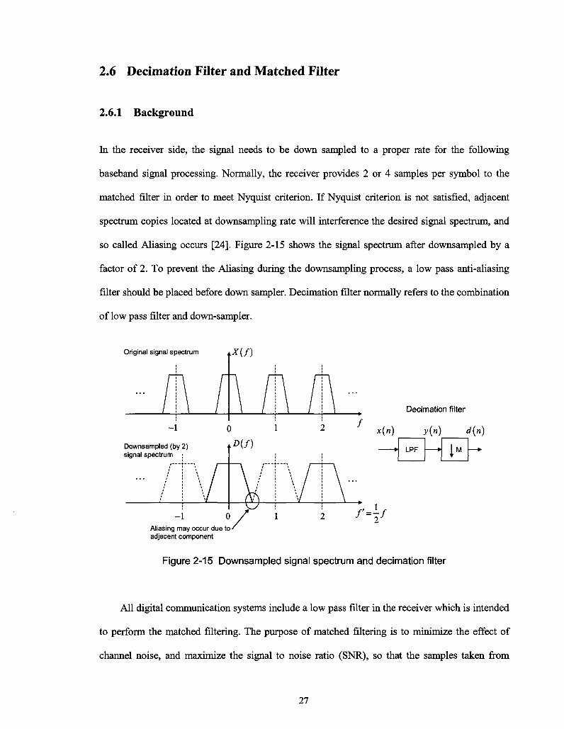
2.6 Decimation Filter and Matched Filter
2.6.1 Background
In the receiver side, the signal needs to be down sampled to a proper rate for the following
baseband signal processing. Normally, the receiver provides 2 or 4 samples per symbol to the
matched filter in order to meet Nyquist criterion. If Nyquist criterion is not satisfied, adjacent
spectrum copies located at downsampling rate will interference the desired signal spectrum, and
so called Aliasing occurs [24]. Figure 2-15 shows the signal spectrum after downsampled by a
factor of 2. To prevent the Aliasing during the downsampling process, a low pass anti-aliasing
filter should be placed before down sampler. Decimation filter normally refers to the combination
of low pass filter and down-sampler.
Original signal spectrum • * ( / )
Decimation filter
y(n) d(n)
Aliasing may occur due to adjacent component
Figure 2-15 Downsampled signal spectrum and decimation filter
All digital communication systems include a low pass filter in the receiver which is intended
to perform the matched filtering. The purpose of matched filtering is to minimize the effect of
channel noise, and maximize the signal to noise ratio (SNR), so that the samples taken from
27
matched filter output are reliable for the detection stage [20] [29]. This is done by shaping the
received signal to obtain a matched waveform of received pluses, which is a distorted version of
transmitted pulses. As mentioned in the previous section, the matched filter is a SQRC filter. If
p(t) is denoted as impulse response of pulse shaping filter, the impulse response of matched
filter is h(t) = p(T-t), where T is the symbol period, and 0 < / < r [20]. Sincep(/) normally
has a symmetric structure, h(t) is identical with p(t). The output of matched filter is sampled at
symbol rate to produce one sample per symbol for the detection path. As long as the sampling
rate, or receiver clock, is synchronous with symbol rate, or transmitter clock, the sampling
instance can reside at peak of signal pulses, where the value is most reliable for the further
processing. The optimum sampling time also corresponds to a clearly-opened eye diagram in the
absence of any channel distortion. If such a requirement is not met, symbol timing recovery is
necessary and will be discussed in detail in chapter 3.
2.6.2 Design and Implementation
To down sample a signal by a factor of M , only every Mth sample will be kept after
downsampling, and all the other samples will be thrown away. As the inserted zeroes in the
interpolation, the discarded samples that do not contribute to the decimation output can be
ignored during filtering process. The polyphase partition is also suitable for decimation filter
structure to reduce the unnecessary computation. First, let us derive the decimation equation, and
see how polyphase is realized. Digital filter transfer function is re-written as
y(n) = x{n)®h(n) = Ydx{n-k)h(k) (2.13) t=o
where h(n) is the filter's impulse response with N = S-M taps. If y(n) is to be down-sampled
by a factor of M, the process can be modeled as
d(n) = y(M-n). (2.14)
28
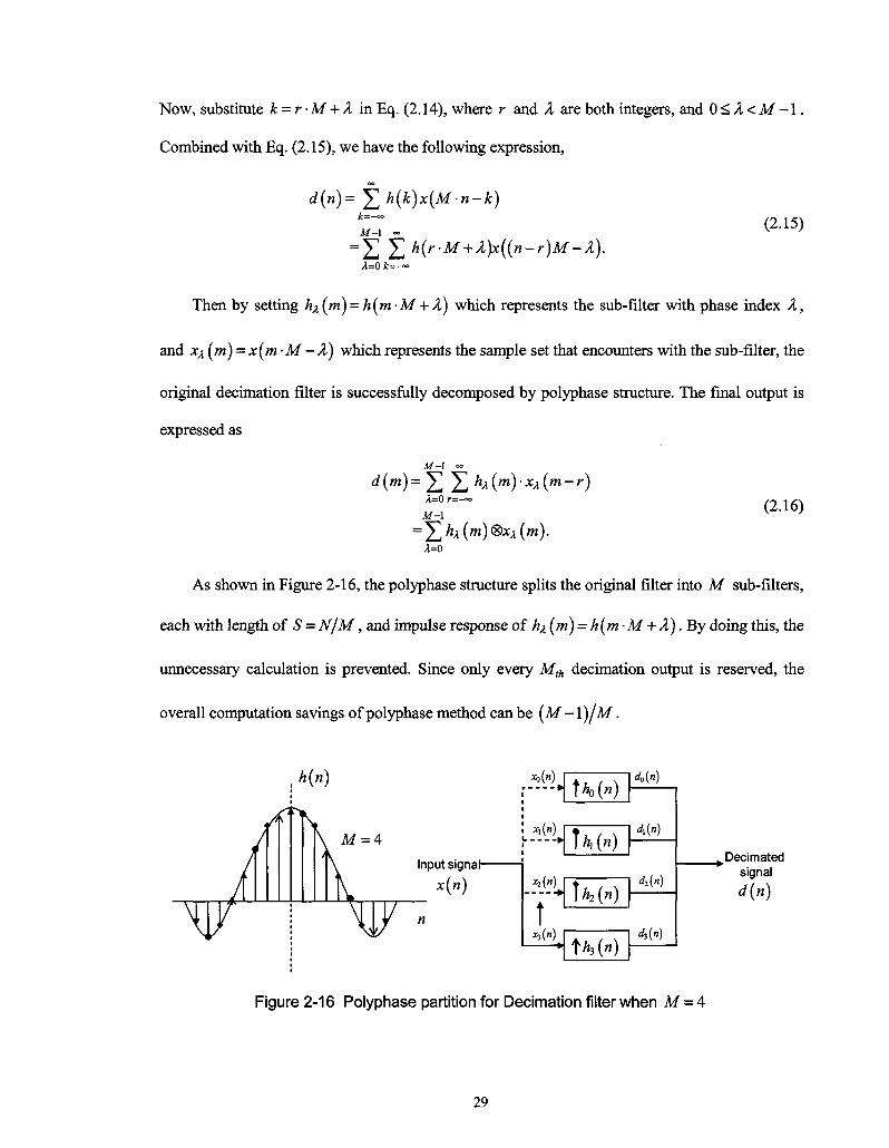
Now, substitute k = r • M + X in Eq. (2.14), where r and X are both integers, and 0 < X < M - 1 .
Combined with Eq. (2.15), we have the following expression,
d(n)= £ h(k)x(M-n-k) k= M-\ ~
(2.15) = Z Z h(r-M + X)x((n-r)M-X).
Then by setting hx(m) = h(m-M + X) which represents the sub-filter with phase index X,
and xx (m) = x(m • M -X) which represents the sample set that encounters with the sub-filter, the
original decimation filter is successfully decomposed by polyphase structure. The final output is
expressed as
M-\ d(m)='YJ X h{™)-xx{m-r)
2=0 r=^» M-\
= YJh{m)®xx{m). (2.16)
x=o
As shown in Figure 2-16, the polyphase structure splits the original filter into M sub-filters,
each with length of S = N/M , and impulse response of hx (m) = h(m • M + X). By doing this, the
unnecessary calculation is prevented. Since only every Mth decimation output is reserved, the
overall computation savings of polyphase method can be (M -\)JM.
. * ( » )
M = 4 Input signal-
x(n)
M")
* i ( « )
»
x3(n)
\k)(n)
U(n)
]h2(n)
fh3(n)
d0(n)
M»)
di(n)
d,(n)
^Decimated signal d\n)
Figure 2-16 Polyphase partition for Decimation filter when M = 4
29
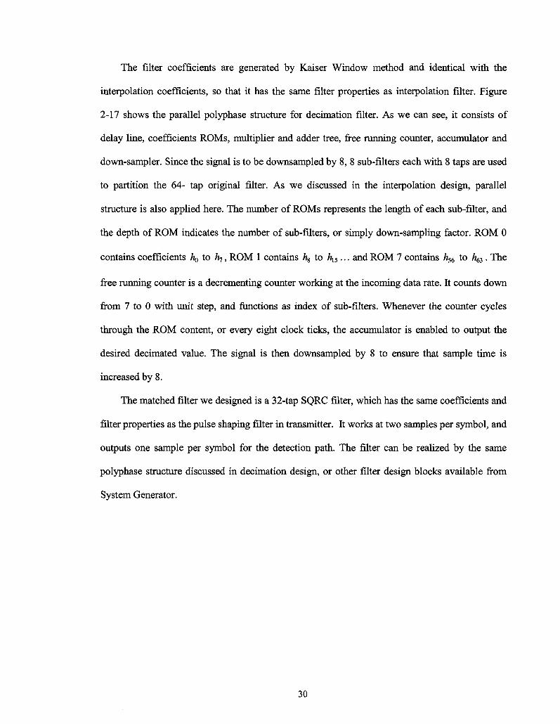
The filter coefficients are generated by Kaiser Window method and identical with the
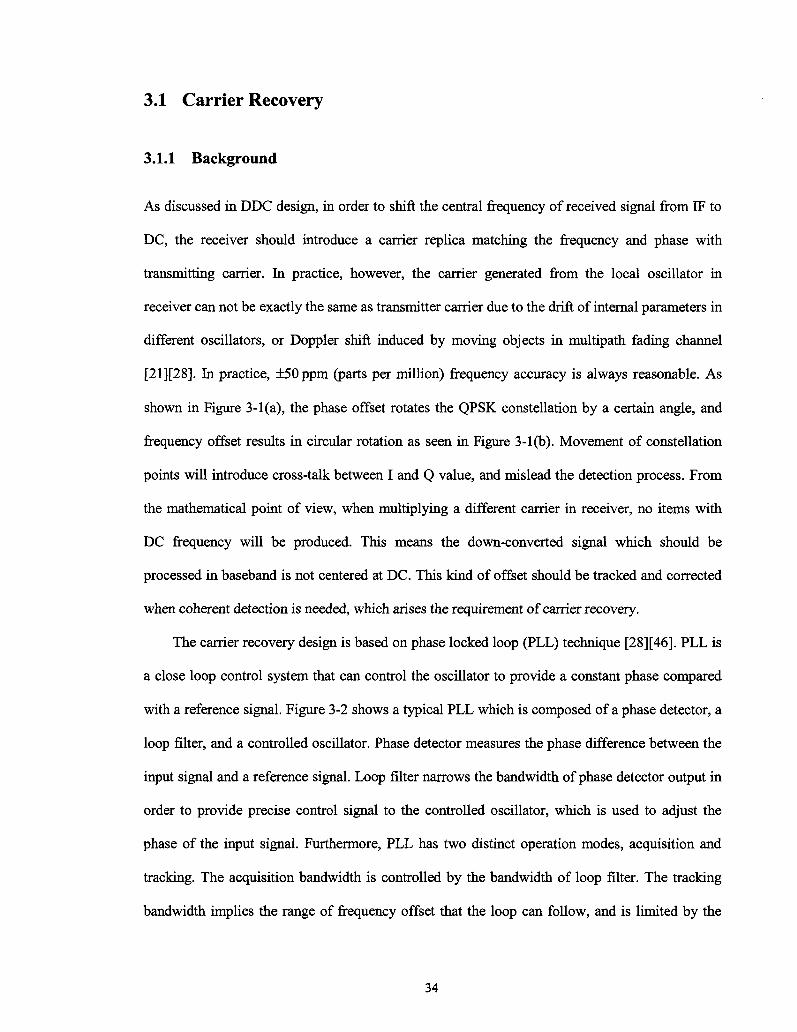
interpolation coefficients, so that it has the same filter properties as interpolation filter. Figure
2-17 shows the parallel polyphase structure for decimation filter. As we can see, it consists of
delay line, coefficients ROMs, multiplier and adder tree, free running counter, accumulator and
down-sampler. Since the signal is to be downsampled by 8, 8 sub-filters each with 8 taps are used
to partition the 64- tap original filter. As we discussed in the interpolation design, parallel
structure is also applied here. The number of ROMs represents the length of each sub-filter, and
the depth of ROM indicates the number of sub-filters, or simply down-sampling factor. ROM 0
contains coefficients h§ to hj, ROM 1 contains h$ to hl5... and ROM 7 contains h56 to h6i. The
free running counter is a decrementing counter working at the incoming data rate. It counts down
from 7 to 0 with unit step, and functions as index of sub-filters. Whenever the counter cycles
through the ROM content, or every eight clock ticks, the accumulator is enabled to output the
desired decimated value. The signal is then downsampled by 8 to ensure that sample time is
increased by 8.
The matched filter we designed is a 32-tap SQRC filter, which has the same coefficients and
filter properties as the pulse shaping filter in transmitter. It works at two samples per symbol, and
outputs one sample per symbol for the detection path. The filter can be realized by the same
polyphase structure discussed in decimation design, or other filter design blocks available from
System Generator.
30
cry Input
with high data rate
Figure 2-17 Parallel structure for polyphase decimation filter
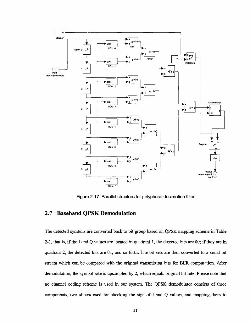
2.7 Baseband QPSK Demodulation
The detected symbols are converted back to bit group based on QPSK mapping scheme in Table
2-1, that is, if the I and Q values are located in quadrant 1, the detected bits are 00; if they are in
quadrant 2, the detected bits are 01, and so forth. The bit sets are then converted to a serial bit
stream which can be compared with the original transmitting bits for BER computation. After
demodulation, the symbol rate is upsampled by 2, which equals original bit rate. Please note that
no channel coding scheme is used in our system. The QPSK demodulator consists of three
components, two slicers used for checking the sign of I and Q values, and mapping them to
31
according decision region (quadrant); a look-up table storing the bit values and a parallel to serial
converter. The structure is shown in Figure 2-18.
d > i
Q
- H :-<[a:bl[-
[a:b]-
addfe"1 f>/ ' s
Out1
ROM Parallel to Serial
Slice 1
Figure 2-18 QPSK baseband demodulator
32
Chapter 3
Synchronization for SISO System
Synchronization is critical in receiver design of a communication system. Two common tasks are
performed for synchronization between transmitter and receiver, which are clock (symbol timing)
recovery and carrier recovery [27] [28].
When coherent demodulation is needed, the baseband signal is derived by convolving the
received signal with a local reference carrier, which has frequency and phase that match the
transmitting carrier. Such an operation performing the carrier matching refers to carrier recovery
(CR). On the other hand, the ultimate task of receiver is to produce an accurate replica of
transmitting symbol sequence from received signal. In a baseband M-PSK or QAM system, the
received signal is passed through a matched filter and then sampled at symbol rate. The optimum
sampling instances correspond to the maximum eyes opening and are located at the peaks of
signal pulses [27]. It is obvious that the reliability of detection depends on the location of
sampling points. Such an operation determining the sample location refers to symbol timing
recovery (STR).
In this chapter, we first introduce the theoretical background of carrier and symbol timing
recovery, respectively. Design and implementation of these two circuits are then explained in
detail. Simulation of one CR algorithm and two STR algorithms are also performed and analyzed,
and the BER performance in AWGN channel is also presented.
33
3.1 Carrier Recovery
3.1.1 Background
As discussed in DDC design, in order to shift the central frequency of received signal from IF to
DC, the receiver should introduce a carrier replica matching the frequency and phase with
transmitting carrier. In practice, however, the carrier generated from the local oscillator in
receiver can not be exactly the same as transmitter carrier due to the drift of internal parameters in
different oscillators, or Doppler shift induced by moving objects in multipath fading channel
[21][28]. In practice, +50ppm (parts per million) frequency accuracy is always reasonable. As
shown in Figure 3-1(a), the phase offset rotates the QPSK constellation by a certain angle, and
frequency offset results in circular rotation as seen in Figure 3-1 (b). Movement of constellation
points will introduce cross-talk between I and Q value, and mislead the detection process. From
the mathematical point of view, when multiplying a different carrier in receiver, no items with
DC frequency will be produced. This means the down-converted signal which should be
processed in baseband is not centered at DC. This kind of offset should be tracked and corrected
when coherent detection is needed, which arises the requirement of carrier recovery.
The carrier recovery design is based on phase locked loop (PLL) technique [28][46]. PLL is
a close loop control system that can control the oscillator to provide a constant phase compared
with a reference signal. Figure 3-2 shows a typical PLL which is composed of a phase detector, a
loop filter, and a controlled oscillator. Phase detector measures the phase difference between the
input signal and a reference signal. Loop filter narrows the bandwidth of phase detector output in
order to provide precise control signal to the controlled oscillator, which is used to adjust the
phase of the input signal. Furthermore, PLL has two distinct operation modes, acquisition and
tracking. The acquisition bandwidth is controlled by the bandwidth of loop filter. The tracking
bandwidth implies the range of frequency offset that the loop can follow, and is limited by the
34
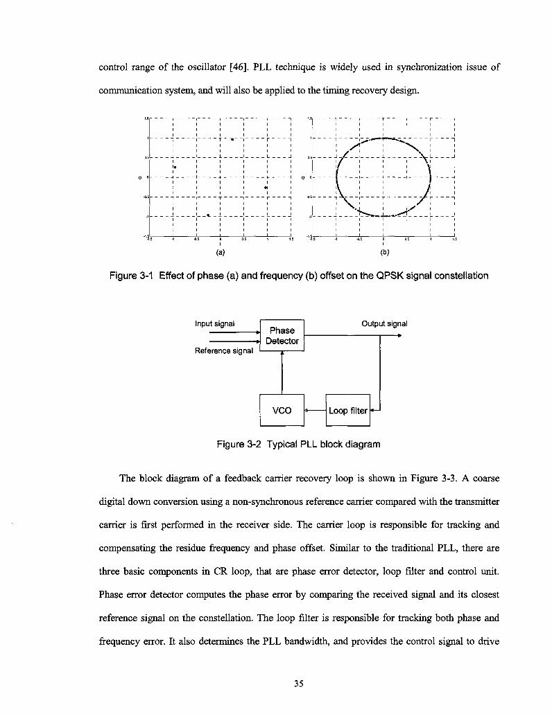
control range of the oscillator [46]. PLL technique is widely used in synchronization issue of
communication system, and will also be applied to the timing recovery design.
1 1
J 1 _ 1 1 _ L J
1* 1 1 1 1 1
1 1 1 1 «l 1
~\ i - T i r I i i i i i i
5 -1 -0.5 0 0.5 1 1.
(a)
Figure 3-1 Effect of phase (a) and frequency (b) offset on the QPSK signal constellation
Input signal »
Reference signal
Phase Detector
, i
vco
Output signal
4 Loop filter
Figure 3-2 Typical PLL block diagram
The block diagram of a feedback carrier recovery loop is shown in Figure 3-3. A coarse
digital down conversion using a non-synchronous reference carrier compared with the transmitter
carrier is first performed in the receiver side. The carrier loop is responsible for tracking and
compensating the residue frequency and phase offset. Similar to the traditional PLL, there are
three basic components in CR loop, that are phase error detector, loop filter and control unit.
Phase error detector computes the phase error by comparing the received signal and its closest
reference signal on the constellation. The loop filter is responsible for tracking both phase and
frequency error. It also determines the PLL bandwidth, and provides the control signal to drive
35
the control unit. By measuring the filtered phase error, the control unit can generate a nearly
constant phase that feedbacks to original data path, and realizes the phase and frequency
adjustment. In analog or hybrid carrier recovery, the control unit is realized by a voltage-
controlled-oscillator (VCO), which can be used to adjust the frequency of local oscillator [28]. On
the FPGA platform, the frequency of reference carrier in the receiver is made fixed, so a fully
digital carrier recovery design is required, and VCO is replaced by a numerical-controlled-
oscillator (NCO).
UL/u
t L
Matched Filter
cos(2xfc- +6)
-jsm(2xfc.+0)
Local Dsci lato r
Kuicuui
t
cos(0)
i i I
-sin(0)
V\\j\J
To detection path
Loop Filter
• >
Phase Error Detector
Figure 3-3 Feedback carrier recovery block diagram
3.1.2 Design and Implementation of CR Loop
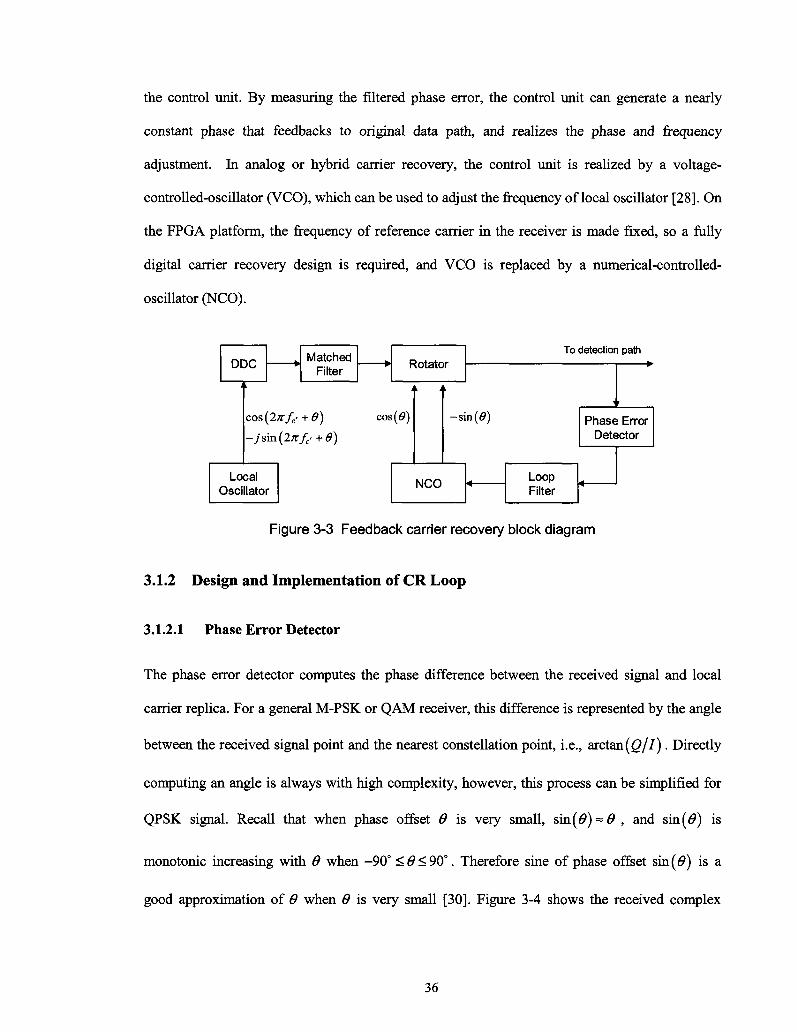
3.1.2.1 Phase Error Detector
The phase error detector computes the phase difference between the received signal and local
carrier replica. For a general M-PSK or QAM receiver, this difference is represented by the angle
between the received signal point and the nearest constellation point, i.e., arctan(g/7). Directly
computing an angle is always with high complexity, however, this process can be simplified for
QPSK signal. Recall that when phase offset 6 is very small, sin(#) = # , and sin(#) is
monotonic increasing with 6 when -90° <#<90° . Therefore sine of phase offset sin(0) is a
good approximation of 6 when 9 is very small [30]. Figure 3-4 shows the received complex
36
signal x + yj and its nearest constellation point m + nj on the QPSK constellation plot. Instead of
calculating the angle 6, we calculate sin(#) which is expressed as following.
sin(0) = sin(or-/?)
= sin a • cos P - cos a • sin fi
_ my — nx
J(x2+y2)(m2
+n2)
(-1,1)
(-1.-1)
i
Q
\ \ \ \ \ \ \
/ /
i
/ /
I/a
x+yj p (1.1)
e£ m + nj • ,
fi\ \ \ \
N S \ \
I
(1.-D
(3.1)
Figure 3-4 Received signal with phase error on QPSK constellation
Since the four constellation points are located at four quadrants, the nearest points are simply
computed by taking the sign of I and Q value of received signal. So the expression can be
modified as
sm (*) = my-nx ^+y%n?W)
_ sign (x)-y — sign(y) • x
" J(x2+y2)(m>+n2)
(3.2)
Based on above equation, the phase error detector can be realized by two sign detectors, two
multipliers and a subtracter. The structure is shown in Figure 3-5. The CR loop with phase error
detector of this structure is normally called Costas loop [20]. This sign-detection based design is
especially suitable for QPSK signal, however, when modulation order goes high, such as 8PSK,
37
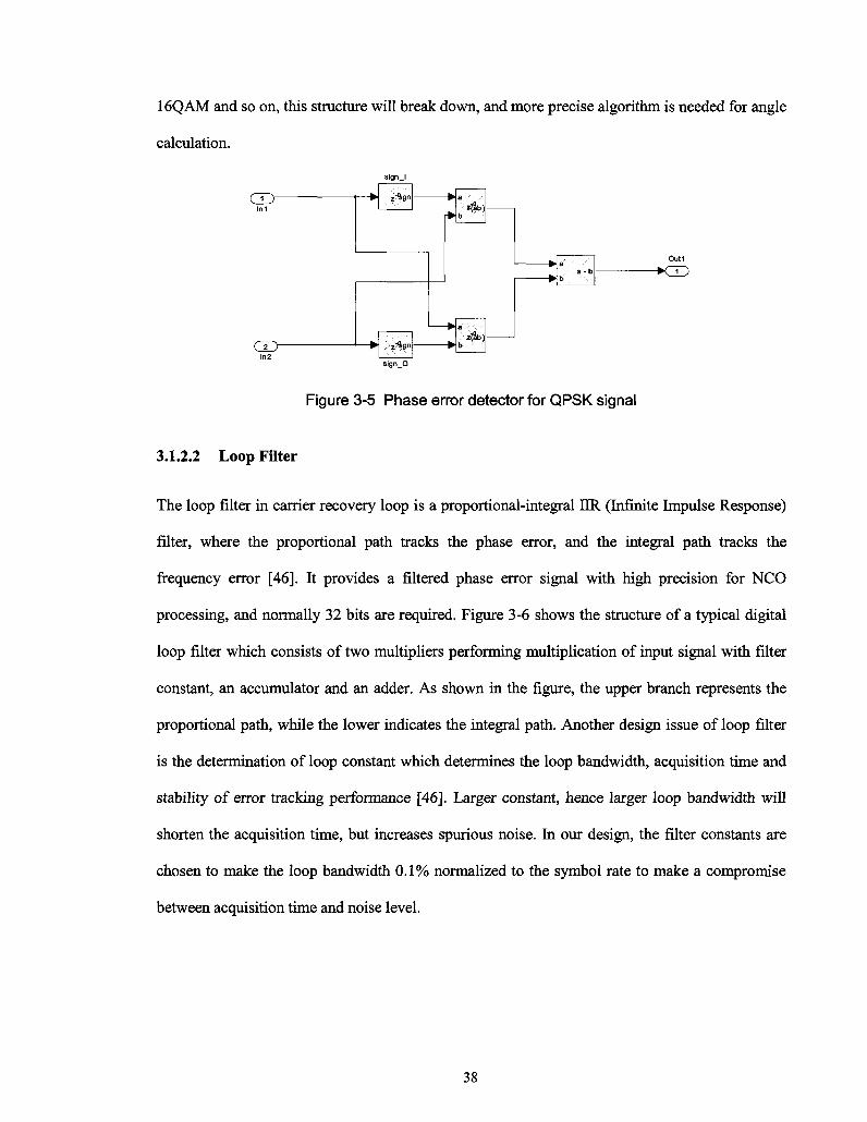
16QAM and so on, this structure will break down, and more precise algorithm is needed for angle
calculation.
_ L - >
V^-J In 2
z;%gn b *
>z"*gn
b 2 ! g b )
a ' / •'- <•
b
i •
a a - b
b •
Out1
kr -! -"! *< - 1 '
sign_Q
Figure 3-5 Phase error detector for QPSK signal
3.1.2.2 Loop FUter
The loop filter in carrier recovery loop is a proportional-integral UR (Infinite Impulse Response)
filter, where the proportional path tracks the phase error, and the integral path tracks the
frequency error [46]. It provides a filtered phase error signal with high precision for NCO
processing, and normally 32 bits are required. Figure 3-6 shows the structure of a typical digital
loop filter which consists of two multipliers performing multiplication of input signal with filter
constant, an accumulator and an adder. As shown in the figure, the upper branch represents the
proportional path, while the lower indicates the integral path. Another design issue of loop filter
is the determination of loop constant which determines the loop bandwidth, acquisition time and
stability of error tracking performance [46]. Larger constant, hence larger loop bandwidth will
shorten the acquisition time, but increases spurious noise. In our design, the filter constants are
chosen to make the loop bandwidth 0.1% normalized to the symbol rate to make a compromise
between acquisition time and noise level.
38
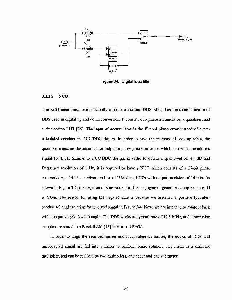
C 1 ) — phase error
3.1.2.3 NCO
fc'0.0.17$
K1
at..b
q z - ' d
register
—•OD Altered ph _err
Figure 3-6 Digital loop filter
The NCO mentioned here is actually a phase truncation DDS which has the same structure of
DDS used in digital up and down conversion. It consists of a phase accumulator, a quantizer, and
a sine/cosine LUT [25]. The input of accumulator is the filtered phase error instead of a pre-
calculated constant in DUC/DDC design. In order to save the memory of look-up table, the
quantizer truncates the accumulator output to a low precision value, which is used as the address
signal for LUT. Similar to DUC/DDC design, in order to obtain a spur level of -84 dB and
frequency resolution of 1 Hz, it is required to have a NCO which consists of a 27-bit phase
accumulator, a 14-bit quantizer, and two 16384-deep LUTs with output precision of 16 bits. As
shown in Figure 3-7, the negation of sine value, i.e., the conjugate of generated complex sinusoid
is taken. The reason for using the negated sine is because we assumed a positive (counter
clockwise) angle rotation for received signal in Figure 3-4. Now, we are intended to rotate it back
with a negative (clockwise) angle. The DDS works at symbol rate of 12.5 MHz, and sine/cosine
samples are stored in a Block RAM [48] in Virtex-4 FPGA.
In order to align the received carrier and local reference carrier, the output of DDS and
unrecovered signal are fed into a mixer to perform phase rotation. The mixer is a complex
multiplier, and can be realized by two multipliers, one adder and one subtracter.
39
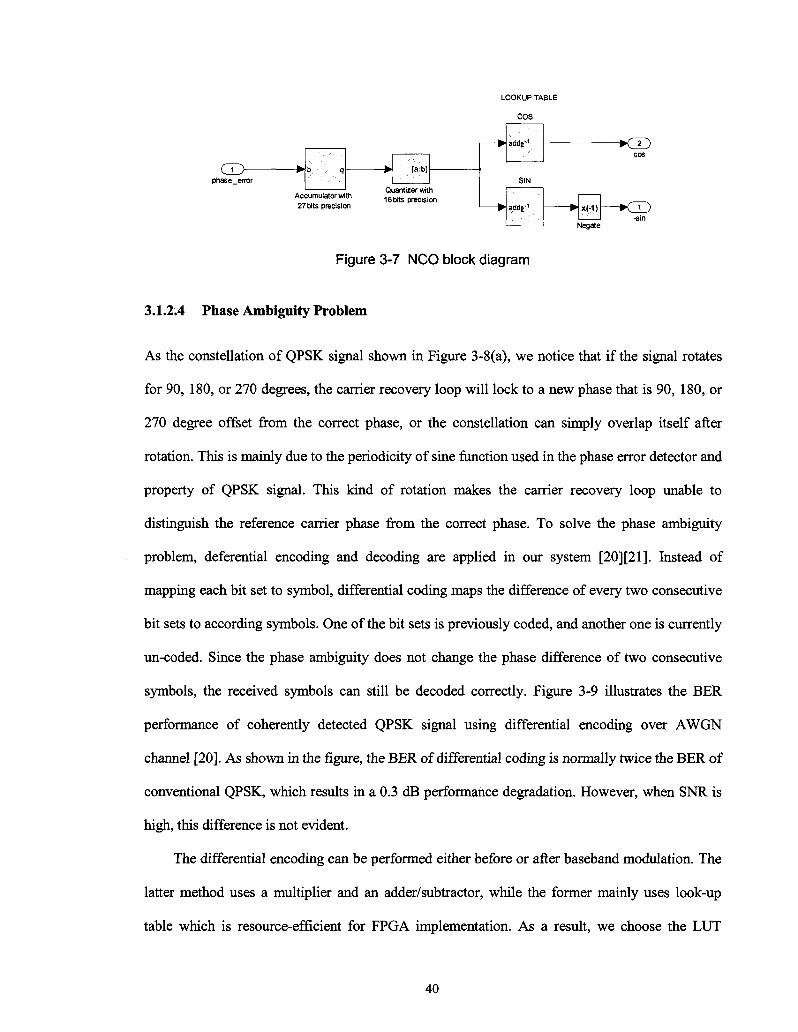
LOOKUP TABLE
COS
r r ^ i phase error
b. \ q
27 bits precision
ta:b]
16 bits precision
addfc'1
SIN
addg-1
r \ *• j
x(-1)
•Janata
-^CD
Figure 3-7 NCO block diagram
3.1.2.4 Phase Ambiguity Problem
As the constellation of QPSK signal shown in Figure 3-8(a), we notice that if the signal rotates
for 90, 180, or 270 degrees, the carrier recovery loop will lock to a new phase that is 90, 180, or
270 degree offset from the correct phase, or the constellation can simply overlap itself after
rotation. This is mainly due to the periodicity of sine function used in the phase error detector and
property of QPSK signal. This kind of rotation makes the carrier recovery loop unable to
distinguish the reference carrier phase from the correct phase. To solve the phase ambiguity
problem, deferential encoding and decoding are applied in our system [20][21]. Instead of
mapping each bit set to symbol, differential coding maps the difference of every two consecutive
bit sets to according symbols. One of the bit sets is previously coded, and another one is currently
un-coded. Since the phase ambiguity does not change the phase difference of two consecutive
symbols, the received symbols can still be decoded correctly. Figure 3-9 illustrates the BER
performance of coherently detected QPSK signal using differential encoding over AWGN
channel [20]. As shown in the figure, the BER of differential coding is normally twice the BER of
conventional QPSK, which results in a 0.3 dB performance degradation. However, when SNR is
high, this difference is not evident.
The differential encoding can be performed either before or after baseband modulation. The
latter method uses a multiplier and an adder/subtractor, while the former mainly uses look-up
table which is resource-efficient for FPGA implementation. As a result, we choose the LUT
40
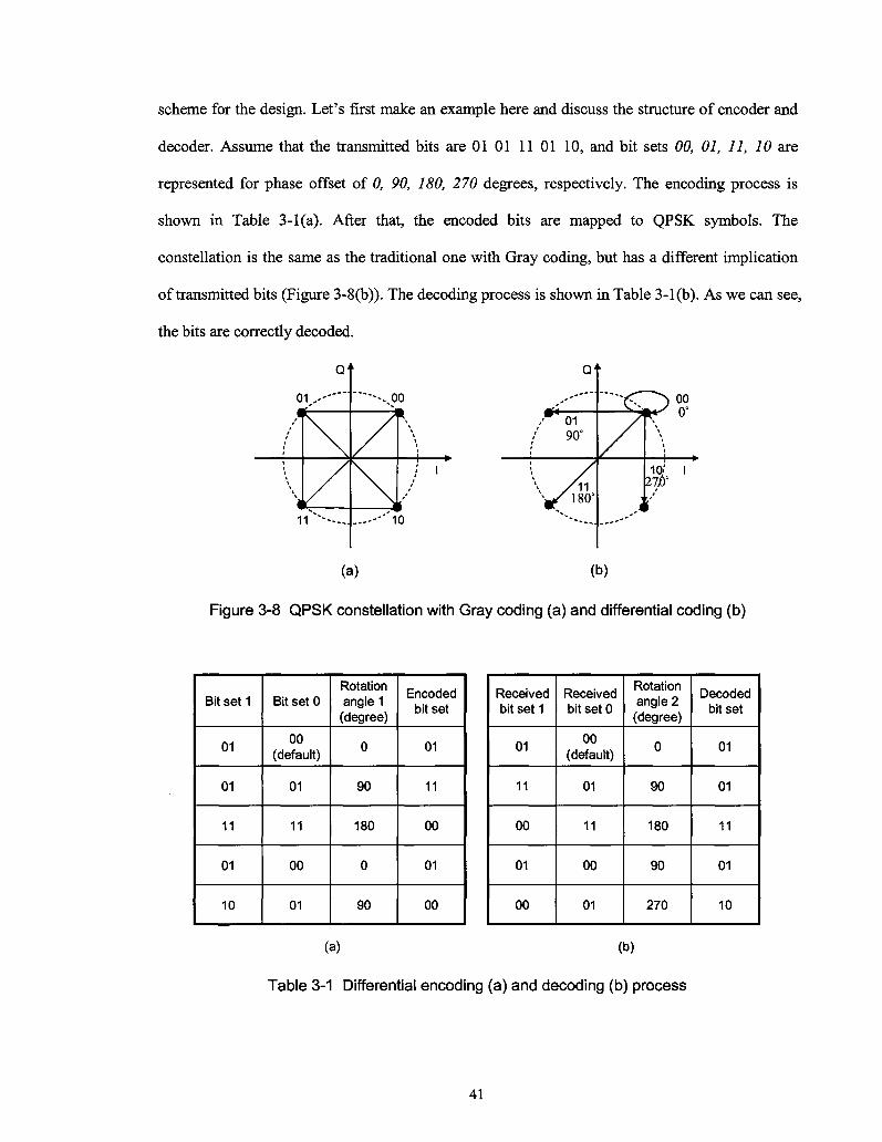
scheme for the design. Let's first make an example here and discuss the structure of encoder and
decoder. Assume that the transmitted bits are 01 01 11 01 10, and bit sets 00, 01, 11, 10 axe
represented for phase offset of 0, 90, 180, 270 degrees, respectively. The encoding process is
shown in Table 3-l(a). After that, the encoded bits are mapped to QPSK symbols. The
constellation is the same as the traditional one with Gray coding, but has a different implication
of transmitted bits (Figure 3-8(b)). The decoding process is shown in Table 3-1 (b). As we can see,
the bits are correctly decoded.
Q '
0 1 , . - - " " '
1
/
> 1
\
/ 1 * • " - - . .
/
\ .—- ' ' 1
0
0
Q
# * •
01 90°
'11 180°
o oo 0°
127,6°
(a) (b)
Figure 3-8 QPSK constellation with Gray coding (a) and differential coding (b)
Bit set 1
01
01
11
01
10
Bit set 0
00 (default)
01
11
00
01
Rotation angle 1 (degree)
0
90
180
0
90
Encoded bit set
01
11
00
01
00
Received bit set 1
01
11
00
01
00
Received bit set 0
00 (default)
01
11
00
01
Rotation angle 2 (degree)
0
90
180
90
270
Decoded bit set
01
01
11
01
10
(a) (b)
Table 3-1 Differential encoding (a) and decoding (b) process
41
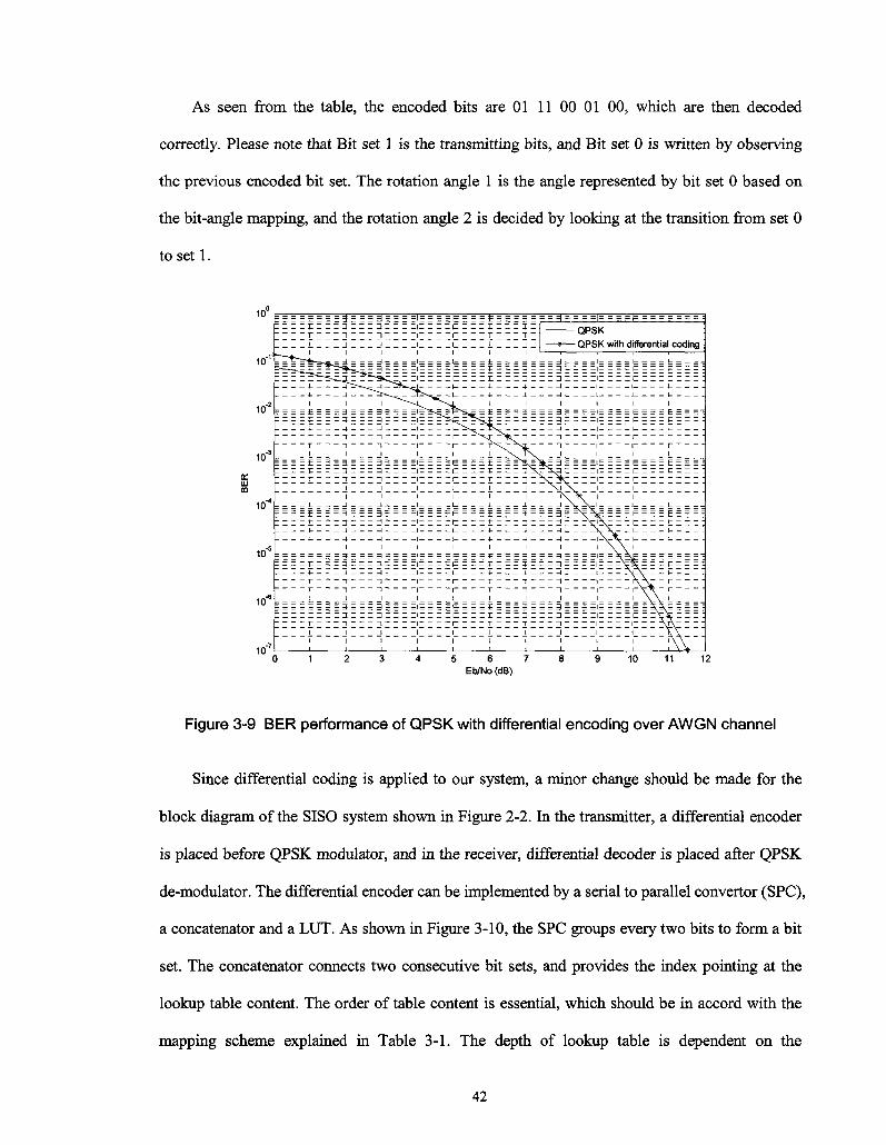
As seen from the table, the encoded bits are 01 11 00 01 00, which are then decoded
correctly. Please note that Bit set 1 is the transmitting bits, and Bit set 0 is written by observing
the previous encoded bit set. The rotation angle 1 is the angle represented by bit set 0 based on
the bit-angle mapping, and the rotation angle 2 is decided by looking at the transition from set 0
to set 1.
10°
10"1'
tr HI CD
10"4
10"5
10"
107
0 1 2 3 4 5 6 7 8 9 10 11 12 Eb/No (dB)
Figure 3-9 BER performance of QPSK with differential encoding over AWGN channel
Since differential coding is applied to our system, a minor change should be made for the
block diagram of the SISO system shown in Figure 2-2. In the transmitter, a differential encoder
is placed before QPSK modulator, and in the receiver, differential decoder is placed after QPSK
de-modulator. The differential encoder can be implemented by a serial to parallel convenor (SPC),
a concatenator and a LUT. As shown in Figure 3-10, the SPC groups every two bits to form a bit
set. The concatenator connects two consecutive bit sets, and provides the index pointing at the
lookup table content. The order of table content is essential, which should be in accord with the
mapping scheme explained in Table 3-1. The depth of lookup table is dependent on the
42
= = = = £ = = = : | = = = : 3 = = = = |= = = = | = z : = = £ = = = =£=: : z -j 3 : 1 - c r~ z~ j -
r i n i i r i
r^Tib"'=r-j!b--^__ _i 1 1 i J 1_
= = ^ = = = =|= = = =|= = = = f = = = :
Annl/
1 1 | J
: ^^"r^^-^^^-sc: t - r r - 2 n - 1 1 r :
r - 1 1 - 1 r ^ \ r 1*. T ~i 1 1 r T r 1 1 1 ^ \ ~ ^ & ' ' ' 1 *
Mil
llll
llll
1 III
h
r-M
WW
m
i 1
in
ULU
llll
mi
MM
HTl
1111
11
11 1 JU
J
"ilT
l llll
1 1 1 1 1 1 1 \ i \ 1 1 1
F =f =1 1 F F =F ^ = -V §|e: 1 F -i r 1 1 1 1 r 1 " \ i \ ' 1
1 1 1 1 1 1 1 1 1 \ \ 1 1 = = = = ^ = = = ^ = = = ^ = = = =l= = = =l= = = = F = = = ^ = = = ^ = = = =l= = \ =M= = = = F = = =T = ^ 3 =1 1 ^p p 5 q 1— -yR F :
E r - = _=r q = 1 =p £_ = _=! q 1 1_ - X A f :
1 1 1 1 1 1 1 1 1 1 V \ 1 1 1 1 1 1 1 1 1 1 i \ \ 1 1 1 1 1 I 1 1 1 1 1 \ i t
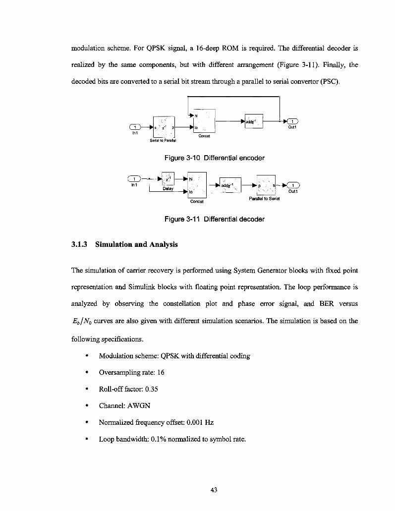
modulation scheme. For QPSK signal, a 16-deep ROM is required. The differential decoder is
realized by the same components, but with different arrangement (Figure 3-11). Finally, the
decoded bits are converted to a serial bit stream through a parallel to serial convertor (PSC).
n~\-In1
V z 1 p k
hi ' v
to •'..•'
Concat
W addf1 • K J D Out1
Serial to Parallel
Figure 3-10 Differential encoder
Q3 In1
N fc :SK Delay
hi -' ' /
add f 1
Concat Parallel to Serial
Figure 3-11 Differential decoder
3.1.3 Simulation and Analysis
1 Out1
The simulation of carrier recovery is performed using System Generator blocks with fixed point
representation and Simulink blocks with floating point representation. The loop performance is
analyzed by observing the constellation plot and phase error signal, and BER versus
Eb/N0 curves are also given with different simulation scenarios. The simulation is based on the
following specifications.
• Modulation scheme: QPSK with differential coding
• Oversampling rate: 16
• Roll-off factor: 0.35
• Channel: AWGN
• Normalized frequency offset: 0.001 Hz
• Loop bandwidth: 0.1% normalized to symbol rate.
43

The received signal constellation before carrier recovery is shown in Figure 3-12(a). As we
can see, the frequency offset causes the constellation to rotate. After carrier recovery is performed,
last 300 of total received 600 symbols are presented in the plot. It is clear that the loop is locked
to a stable status, and four QPSK signal points are presented on the constellation. The phase
ambiguity problem is prevented by using differential coding, so that these points seen on the
constellation are most reliable for the detection stage.
f^ff**W*WHV - -t - - •
f V
1 "V - - r 1 1 - - >«- r
\ : i \y \
0.E
o.e
0.4
0.2
o 0
•02
-0.4
•0.6
•0.8
•1
~ i n T r i - ] T ~ r i n i i i i i i i i i i I J 1 L l J ± 1_ 1 _l
:# v : i - i T r i - i T r i - i
i J x i_ i J i i_ i _i
i i i i i i i i i i 1 1 T 1 1 1 T 1 1 1 1 1 1 1 1 1 1 1 I 1 1 1 — + — 1 1 1 — + — i 1 1
1 1 1 1 1 1 1 1 1 I 1 1 1 1 1 1 1 1 1 1
1 1 4- 1 1 1 4- 1 1 1
: * ! : : : : : : * : : - " i n T r i n T ~ r i "i
i i i i i i i i i i -1 -0.8 -0.6 -0.4 -0.2 0 0.2 0.4 0.6 0.8 1
(a) (b)
Figure 3-12 Signal constellation before (a) and after (b) carrier recovery
A good observation point for watching loop behavior is the phase error as provided into the
NCO [46]. Ideally this term should become zero when the loop reaches a stable locked status. The
phase error signal in the absence of channel distortion is shown in Figure 3-13. After about 300
symbols, the error signal converges to 0, and keeps up and down in a small range due to the
randomness of transmitted signal and spurious noise induced by loop itself. NCO can then
provide a nearly constant signal which represents the frequency and phase offset between the
transmitter carrier and local reference. The 300 symbols is the acquisition time of our carrier
recovery loop. After that, the loop is successfully locked.
44
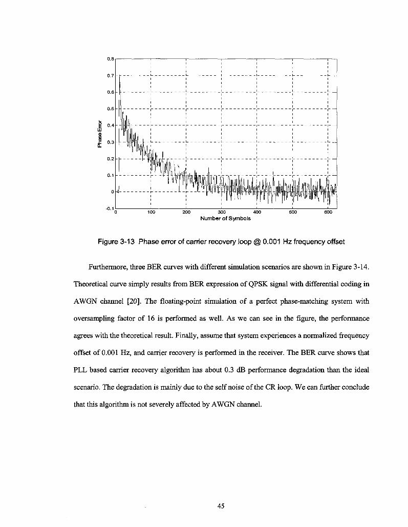
0.8
200 300 400 Number of Symbols
Figure 3-13 Phase error of carrier recovery loop @ 0.001 Hz frequency offset
Furthermore, three BER curves with different simulation scenarios are shown in Figure 3-14.
Theoretical curve simply results from BER expression of QPSK signal with differential coding in
AWGN channel [20]. The floating-point simulation of a perfect phase-matching system with
oversampling factor of 16 is performed as well. As we can see in the figure, the performance
agrees with the theoretical result. Finally, assume that system experiences a normalized frequency
offset of 0.001 Hz, and carrier recovery is performed in the receiver. The BER curve shows that
PLL based carrier recovery algorithm has about 0.3 dB performance degradation than the ideal
scenario. The degradation is mainly due to the self noise of the CR loop. We can further conclude
that this algorithm is not severely affected by AWGN channel.
45
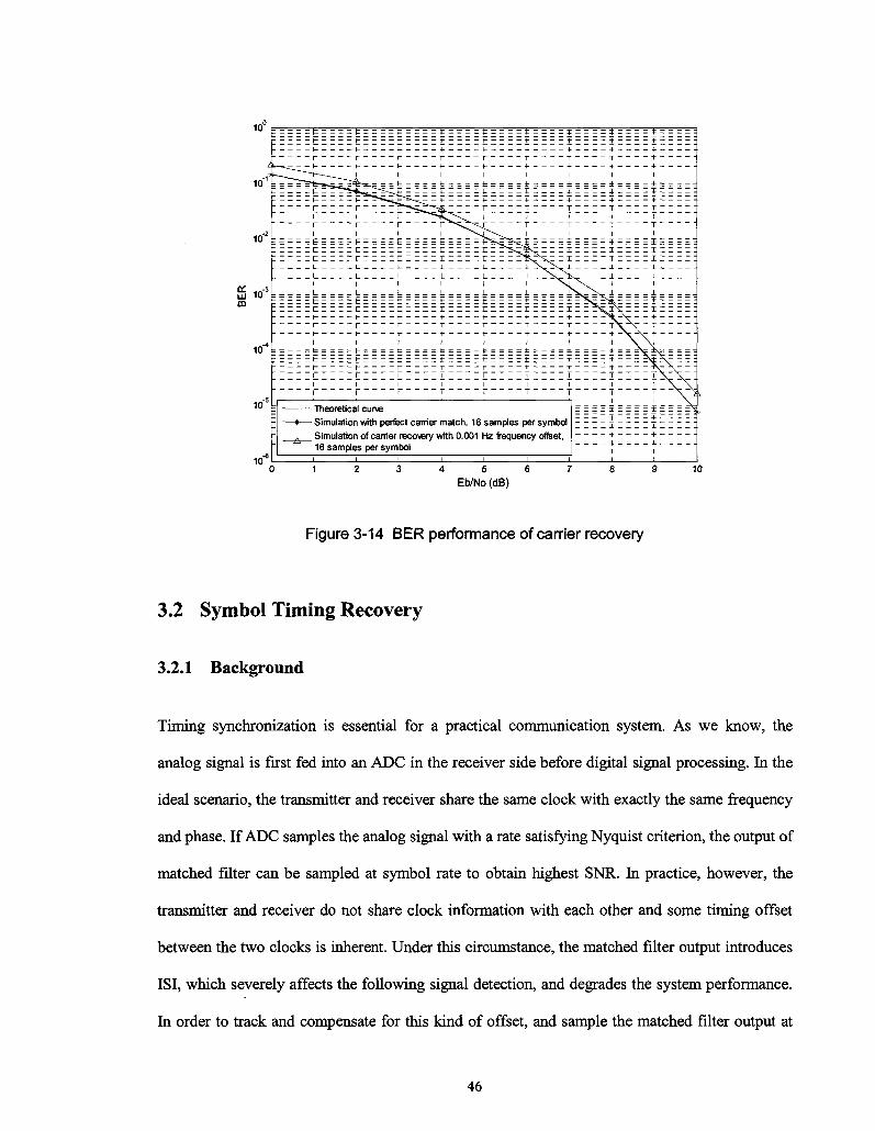
10
10
10
S 10"3
CO
10
10
10
_ £ = t_ £ 1 = t J. 1 1 _ I 1 1 1 1 1- 1- + - T ; 1-
z--- - pT=~!T*5-E|>^^t : : : : j : : : = : f ; : : : j : : : : : i : " : j :
i i i ^ - ^ ^ J T * ^ i i i i i i i ^ " " ^ ^ ^ T ^ ^ i i i i r ~ r r r^*\^^C T ~ T T
+
E E E ± H E E E ^
+ T _ ; T
I | I J J 4- - X ^ N _ 4- 4- -IN
I
Mil
Mil
Mil
Mil
mi—
M
il M
il
mi—
M
il M
il I
III
mi—
MM
H-ll
l+ll
Mil
Mil
Mil
Mil
I I I I I I I I _ fc t fc t fc t ± ±_ I i | i H •{ -t + —
4-
E E E ^ = = E E 1 I _ I
AJL===, S y i s: .
I I I I I 1 I I I \ _ \ 1 1 1 1 1 1 1 1 1 \ _ \ 1 1 1 1 1 1 1
= Theoretical curve
A Simulation of carrier reco\ery with 0.001 Hz frequency offset. 16 samples per symbol
i i i i i i i
i I \
4 _
|
4- .
I
4 5 6 Eb/No (dB)
10
Figure 3-14 BER performance of carrier recovery
3.2 Symbol Timing Recovery
3.2.1 Background
Timing synchronization is essential for a practical communication system. As we know, the
analog signal is first fed into an ADC in the receiver side before digital signal processing. In the
ideal scenario, the transmitter and receiver share the same clock with exactly the same frequency
and phase. If ADC samples the analog signal with a rate satisfying Nyquist criterion, the output of
matched filter can be sampled at symbol rate to obtain highest SNR. In practice, however, the
transmitter and receiver do not share clock information with each other and some timing offset
between the two clocks is inherent. Under this circumstance, the matched filter output introduces
ISI, which severely affects the following signal detection, and degrades the system performance.
In order to track and compensate for this kind of offset, and sample the matched filter output at
46
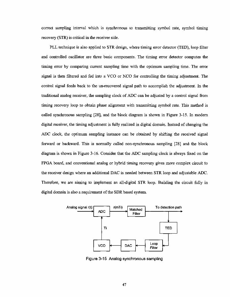
correct sampling interval which is synchronous to transmitting symbol rate, symbol timing
recovery (STR) is critical in the receiver side.
PLL technique is also applied to STR design, where timing error detector (TED), loop filter
and controlled oscillator are three basic components. The timing error detector computes the
timing error by comparing current sampling time with the optimum sampling time. The error
signal is then filtered and fed into a VCO or NCO for controlling the timing adjustment. The
control signal feeds back to the un-recovered signal path to accomplish the adjustment. In the
traditional analog receiver, the sampling clock of ADC can be adjusted by a control signal from
timing recovery loop to obtain phase alignment with transmitting symbol rate. This method is
called synchronous sampling [28], and the block diagram is shown in Figure 3-15. In modern
digital receiver, the timing adjustment is fully realized in digital domain. Instead of changing the
ADC clock, the optimum sampling instance can be obtained by shifting the received signal
forward or backward. This is normally called non-synchronous sampling [28] and the block
diagram is shown in Figure 3-16. Consider that the ADC sampling clock is always fixed on the
FPGA board, and conventional analog or hybrid timing recovery gives more complex circuit to
the receiver design where an additional DAC is needed between STR loop and adjustable ADC.
Therefore, we are aiming to implement an all-digital STR loop. Building the circuit fully in
digital domain is also a requirement of the SDR based system.
signal r(t) A u o
i
Ti
Vv. J\J
r(mTi) Matched Filter
u r\o
To detection path
' '
TED
Loop Filter
Figure 3-15 Analog synchronous sampling
47
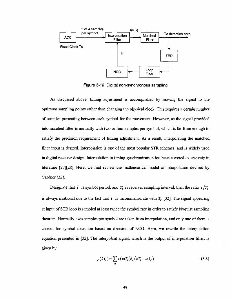
2 or 4 samples r(kTi)
ADC per symbol
Fixed Clock Ts
Interpolation Filter
i .
Matched Filter
Ti
INL.U Loop Filter
To detection path
' '
TED
Figure 3-16 Digital non-synchronous sampling
As discussed above, timing adjustment is accomplished by moving the signal to the
optimum sampling points rather than changing the physical clock. This requires a certain number
of samples presenting between each symbol for the movement. However, as the signal provided
into matched filter is normally with two or four samples per symbol, which is far from enough to
satisfy the precision requirement of timing adjustment. As a result, interpolating the matched
filter input is desired. Interpolation is one of the most popular STR schemes, and is widely used
in digital receiver design. Interpolation in timing synchronization has been covered extensively in
literature [27][28]. Here, we first review the mathematical model of interpolation devised by
Gardner [32].
Designate that T is symbol period, and Ts is receiver sampling interval, then the ratio T/Ts
is always irrational due to the fact that T is incommensurate with 7 [32]. The signal appearing
at input of STR loop is sampled at least twice the symbol rate in order to satisfy Nyquist sampling
theorem. Normally, two samples per symbol are taken from interpolation, and only one of them is
chosen for symbol detection based on decision of NCO. Here, we rewrite the interpolation
equation presented in [32]. The interpolant signal, which is the output of interpolation filter, is
given by
y{kTi) = Ydx{mTs)hI{kTi-mTs) (3.3)
48
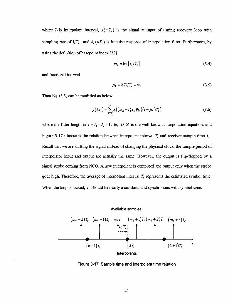
where Tt is interpolant interval, x(mTs) is the signal at input of timing recovery loop with
sampling rate of l/Ts, and hj (nTs) is impulse response of interpolation filter. Furthermore, by
using the definition of basepoint index [32]
mA=int[7]/rs] (3.4)
and fractional interval
{lk=kTi/Ts-mk (3.5)
Then Eq. (3.3) can be modified as below
y(kTi) = jjx{{mk-i)Ts)hI{{i + fik)Ts) (3.6) <=/„
where the filter length is I = Ix -I0 +1 . Eq. (3.6) is the well known interpolation equation, and
Figure 3-17 illustrates the relation between interpolant interval 7) and receiver sample time Ts.
Recall that we are shifting the signal instead of changing the physical clock, the sample period of
interpolator input and output are actually the same. However, the output is flip-flopped by a
signal strobe coming from NCO. A new interpolant is computed and output only when the strobe
goes high. Therefore, the average of interpolant interval 7] represents the estimated symbol time.
When the loop is locked, 7J should be nearly a constant, and synchronous with symbol time.
Available samples
(mk-2)Ts {mk-\)Ts mkTs (mk+l)Ts(mk+2)Ts (mk+3)Ts
VMkTs
(k-l)T, \kTt
Interpolants
(*+i)r,
Figure 3-17 Sample time and interpolant time relation
49
3.2.2 Main Components in STR loop
In a PLL based STR design using interpolation technique, interpolator/matched filter, timing error
detector, loop filter and NCO are the key components of STR loop. In this section, these
components are discussed except for loop filter, which has been introduced in carrier recovery
design. Moreover, two different algorithms for timing error detection are emphasized. The
detailed design and implementation of STR loop will be introduced in the next section.
3.2.2.1 Interpolator
In the widely proposed STR schemes using interpolation technique, the matched filter is placed
either inside or outside the loop, and different methods for interpolation filter design are also well
introduced [27][28][33][41]. In our design, the matched filter and interpolation filter are rolled
into a same stage where a so called interpolated matched filter is used for the timing adjustment
[35][42]. The new matched filter is actually an upsampled version of original matched filter, and
each interpolant between each sample can represent a different timing offset with respect to
symbol interval. When polyphase structure is further applied to the filter design, each sub filter
corresponds to a different timing offset. In other words, selecting the correct sub filter means
making the correct timing adjustment.
Let us now examine how polyphase can be applied to the timing recovery design. Recall the
polyphase issue we discussed in interpolation filter design, the impulse response of sub-filter is
expressed as
hx(n) = h{n-L + X) (3.7)
whereL is upsampling factor, and X is an integer with 0 < 2 < Z, - 1 . As we can see, sub-filter
can be derived from original filter with a phase index X. If L sub-filters are used for polyphase
50
structure of timing recovery, the impulse response of mth (0 < m < Z) sub-filter can be expressed
as
hm(nTs) = hI(nTs+({m/L)Ts)) (3.8)
where hj (nTs) is impulse response of original interpolation filter. Then the output of the mth
sub-filter is given by
ym(kTi)= 5X(»-i)r,)fe/ i=-2P
'• y
f A ( 3 - 9 )
nTs+—T. L
where P is the symbol span of original interpolation filter, and oversampling factor is 2. Since
the interpolants are computed and output at time kTt = (mk + juk )TS, we can conclude that as long
as n = mk, the following equation is established
ym{kTi)= y(mkTs +{m/L)Ts)
= y(mkTs+/lkTs)
Eq. (3.10) clearly shows that the ratio m/L plays the same role as juk . Furthermore, instead
of computing explicitly, basepoint mkis indicated by the signal strobe of NCO in order to align
the correct input sample set with the filter coefficients set.
3.2.2.2 Timing Error Detector
Timing error detector (TED) computes the timing error based on the comparison of current
sample timing and estimated symbol timing. Two common structures exist for timing detection
using PLL technique, that are Decision Directed (DD) structure which uses the data decision to
perform detection, and Non-data Aided (NDA) structure, where the detection is independent of
the data decision [28]. Different types of TED designs are introduced broadly in literature. Here,
we discuss and analyze two algorithms mostly used in hardware implementation for timing error
51
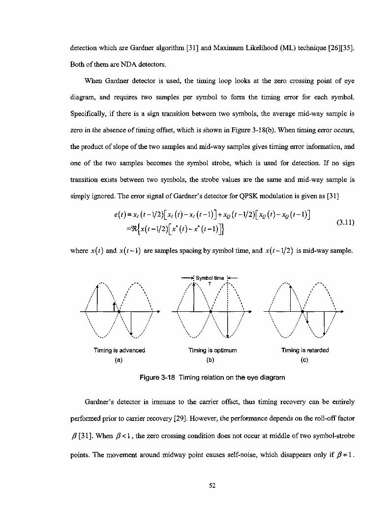
detection which are Gardner algorithm [31] and Maximum Likelihood (ML) technique [26] [35].
Both of them are NDA detectors.
When Gardner detector is used, the timing loop looks at the zero crossing point of eye
diagram, and requires two samples per symbol to form the timing error for each symbol.
Specifically, if there is a sign transition between two symbols, the average mid-way sample is
zero in the absence of timing offset, which is shown in Figure 3-18(b). When timing error occurs,
the product of slope of the two samples and mid-way samples gives timing error information, and
one of the two samples becomes the symbol strobe, which is used for detection. If no sign
transition exists between two symbols, the strobe values are the same and mid-way sample is
simply ignored. The error signal of Gardner's detector for QPSK modulation is given as [31]
e(t) = xI{t-l/2)[xI(t)-xI(t-l)] + xe(t-l/2)[xQ(t)-xQ(t-l)]
=9t{jc(f-l/2)[y(0-**('-!)]} (3.11)
where x(t) and x(t-\) are samples spacing by symbol time, and x(t-l/2) is mid-way sample.
1
/
f"\ \ ' I
1 V > !*
/ '*
/
' /
Timing is advanced
(a)
S\
1
Symbol time
\ ' ! * > ' ! »
' F
V.*' ' V ;.''
Timing is optimum
(b)
/ > ' » / > ' >
v »
\ A /
\./ \y Timing is retarded
(c)
Figure 3-18 Timing relation on the eye diagram
Gardner's detector is immune to the carrier offset, thus timing recovery can be entirely
performed prior to carrier recovery [29]. However, the performance depends on the roll-off factor
/? [31]. When / ? < 1 , the zero crossing condition does not occur at middle of two symbol-strobe
points. The movement around midway point causes self-noise, which disappears only if /? = 1.
52
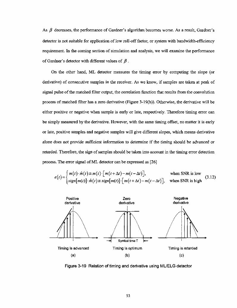
As /? decreases, the performance of Gardner's algorithm becomes worse. As a result, Gardner's
detector is not suitable for application of low roll-off factor, or system with bandwidth-efficiency
requirement. In the coming section of simulation and analysis, we will examine the performance
of Gardner's detector with different values of fi .
On the other hand, ML detector measures the timing error by computing the slope (or
derivative) of consecutive samples in the receiver. As we know, if samples are taken at peak of
signal pulse of the matched filter output, the correlation function that results from the convolution
process of matched filter has a zero derivative (Figure 3-19(b)). Otherwise, the derivative will be
either positive or negative when sample is early or late, respectively. Therefore timing error can
be simply measured by the derivative. However, with the same timing offset, no matter it is early
or late, positive samples and negative samples will give different slopes, which means derivative
alone does not provide sufficient information to determine if the timing should be advanced or
retarded. Therefore, the sign of samples should be taken into account in the timing error detection
process. The error signal of ML detector can be expressed as [26]
f m(t)-m(t)Bm(t)-\m(t + At)-m(t-At)~\, whenSNRislow e[t) = < r (3.12)
I sign[m(t)] -m(t) = sign\m(f)\ • \jn{t + At)-m{t- At)], when SNR is high
Positive derivative
Timing is advanced
(a)
Zero derivative
Symbol time T
Timing is optimum
(b)
Negative derivative
Timing is retarded
(c)
Figure 3-19 Relation of timing and derivative using ML/ELG detector
53
The ML timing recovery process minimizes the above error, which is the product of matched
filter output m(t) and its derivative m(t). We also note that when SNR is very low, the sample
itself is more reliable rather than its sign. In practical design, we do not bother the switching and
simply take the sign value for the whole SNR range [26]. The early-late-gate (ELG) algorithm
gives approximation of ML approach and is widely used in the early days. It normally operates
with three samples per symbol time, where two of them are time advanced and delayed
respectively to an intermediate sample point. By comparing the difference between the 'early'
and 'late' samples, this algorithm can form the first central difference of matched filter output
[26] [29]. In modern receiver design, instead of using two additional sub filters to form the early
and late sample, a single filter whose impulse response is given by the derivative of matched
filter's impulse response is used [26]. As a result, three filter stages are replaced by two filters
which are matched filter and its derivative filter, for each timing error calculation. These two
filters are both working at two samples per symbol, and the product of their output forms the
timing error during each symbol time. Compared with Gardner's detector, ML detector is not
independent with carrier offset but gives better SNR and BER performance. When ML timing
error detector is applied in the receiver, carrier recovery loop should be placed inside the timing
recovery loop, which is shown in Figure 2-2.
3.2.2.3 NCO
The task of NCO is to determine basepoint index mk and fractional interval juk . As mentioned
before, the former represents the correct set of signal samples, and the latter indicates the correct
set of filter coefficients. The NCO is actually a decrementing modulo-1 counter. The NCO
output can be written as
c(#i + l) = [c(#i)-w(n)]modl (3.13)
54
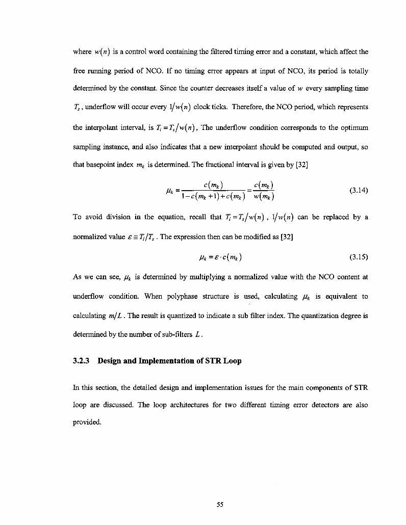
where w(n) is a control word containing the filtered timing error and a constant, which affect the
free running period of NCO. If no timing error appears at input of NCO, its period is totally
determined by the constant. Since the counter decreases itself a value of w every sampling time
7^, underflow will occur every l/w(n) clock ticks. Therefore, the NCO period, which represents
the interpolant interval, is 7] =Ts/w(n), The underflow condition corresponds to the optimum
sampling instance, and also indicates that a new interpolant should be computed and output, so
that basepoint index mk is determined. The fractional interval is given by [32]
l-c{mk+\) + c{mk) w{mk)
To avoid division in the equation, recall that Ti=Tsjw{n) , \/w(n) can be replaced by a
normalized value e = Tt/Ts. The expression then can be modified as [32]
juk=e-c(mk) (3.15)
As we can see, juk is determined by multiplying a normalized value with the NCO content at
underflow condition. When polyphase structure is used, calculating juk is equivalent to
calculating m/L . The result is quantized to indicate a sub filter index. The quantization degree is
determined by the number of sub-filters L.
3.2.3 Design and Implementation of STR Loop
In this section, the detailed design and implementation issues for the main components of STR
loop are discussed. The loop architectures for two different timing error detectors are also
provided.
55

3.2.3.1 Interpolated Matched Filter
The parallel polyphase structure is applied to interpolated matched filter design. The sub filter
index is provided by NCO instead of a free running counter, and the filter output is enabled by a
strobe signal indicating underflow condition of NCO content. As mentioned in [40], in order to
obtain an acceptable implementation loss of 0.12 dB, which is due to timing quantization in NCO,
the desired normalized timing resolution is 1/33 for 4-QAM modulation with a roll off factor of
0.3. Since our system is based on QPSK with a roll off factor of 0.35, we choose 32 sub filters for
the implementation. Note that increasing the timing resolution can not compensate other kinds of
implementation loss. The original 32-tap matched filter is then upsampled by 32 to produce an
interpolated matched filter with 1024 coefficients. The coefficients are generated by Matlab filter
design tool, and stored in 32 LUTs each with depth of 32.
3.2.3.2 Timing Error Detector
We designed two timing error detectors as previously discussed. When ML detector is used, a
derivative matched filter realized by the same parallel polyphase structure is required, and the
coefficients are obtained by convolving the matched filter coefficients with sequence [-1 0 l ] .
Both of these two filters are working at two samples per symbol, and the product of their output
gives the estimated timing error. The sign of matched filter output is taken for large SNR
approximation. Figure 3-20 shows the structure of STR loop using ML detector. On the other
hand, the use of Gardner's detector reduces hardware utilization since only a single matched filter
is necessary as compared to two in ML detector. Figure 3-21 shows the structure of STR loop
using Gardner's detector. Based on Eq. (3.11), the implementation of Gardner's detector is
relatively easy, where delay blocks, 2 multipliers, and 3 adders/subtractors can realize the
function. The circuit is shown in Figure 3-22.
56
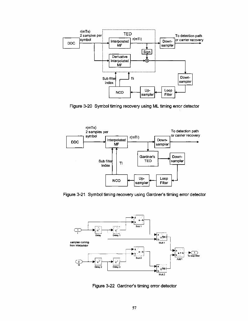
DDC
r(mTs) j 2 samples per'; symbol j
TED
Interpolated MF
Derivative Interpolated
MF
r(mTi) |
Sign
_/&
Down-sampler
To detection path or carrier recovery
Sub filte Index
1
I I O U
Ti
Up-sampler
4 Loop Filter
Down-sampler
Figure 3-20 Symbol timing recovery using ML timing error detector
DDC
r(mTs) 2 samples per
symbol Interpolated MF
i
Sub filtei lnd°*
L i
Ti
NCO
r(mTi)
4
1
Gardner's TED
Up-sampler
4
Down-sampler
Loop Filter
To detection path or carrier recovery
Down-sampler
4—
Figure 3-21 Symbol timing recovery using Gardner's timing error detector
samples coming from interpolator
>i\ Delay
>*:(
a \ ' •'' a - b
e . .
Delay 1 /z'feb) b, - < \
• ^
-±_J <•£' Delay 2
•i'\
a\ '.. -a - b
b
e . _
Delay 3 ' — • a-' v '- ' z-^b)
b
' a + b b ,- To loop filter
Figure 3-22 Gardner's timing error detector
57
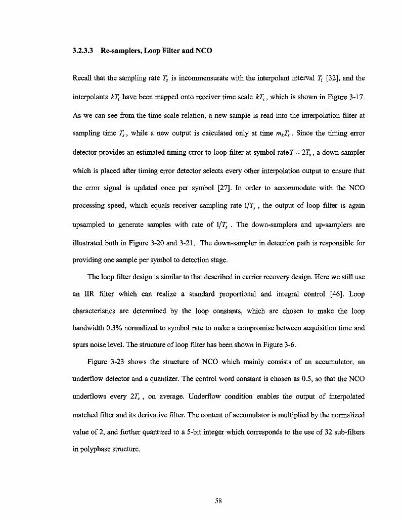
3.2.3.3 Re-samplers, Loop Filter and NCO
Recall that the sampling rate Ts is incommensurate with the interpolant interval Tt [32], and the
interpolants kTt have been mapped onto receiver time scale kTs, which is shown in Figure 3-17.
As we can see from the time scale relation, a new sample is read into the interpolation filter at
sampling time Ts, while a new output is calculated only at time mkTs. Since the timing error
detector provides an estimated timing error to loop filter at symbol rater ~ 2TS, a down-sampler
which is placed after timing error detector selects every other interpolation output to ensure that
the error signal is updated once per symbol [27]. In order to accommodate with the NCO
processing speed, which equals receiver sampling rate 1/7 , the output of loop filter is again
upsampled to generate samples with rate of l/Ts . The down-samplers and up-samplers are
illustrated both in Figure 3-20 and 3-21. The down-sampler in detection path is responsible for
providing one sample per symbol to detection stage.
The loop filter design is similar to that described in carrier recovery design. Here we still use
an IIR filter which can realize a standard proportional and integral control [46]. Loop
characteristics are determined by the loop constants, which are chosen to make the loop
bandwidth 0.3% normalized to symbol rate to make a compromise between acquisition time and
spurs noise level. The structure of loop filter has been shown in Figure 3-6.
Figure 3-23 shows the structure of NCO which mainly consists of an accumulator, an
underflow detector and a quantizer. The control word constant is chosen as 0.5, so that the NCO
underflows every 2TS , on average. Underflow condition enables the output of interpolated
matched filter and its derivative filter. The content of accumulator is multiplied by the normalized
value of 2, and further quantized to a 5-bit integer which corresponds to the use of 32 sub-filters
in polyphase structure.
58
crx-out_en
ax-poly_index
Slice
[3*1
'\/i
Relational
Vi
CMult
Sub
d z - 1 q
Register
Constant
Add
1 ' t b ,
timing _en
Figure 3-23 NCO in symbol timing recovery loop
3.2.4 Simulation and Analysis
In this section, simulation results of timing recovery using two different TED designs are
presented. Comparison of Gardner's detector with different roll-off factors is also made. The loop
performance is analyzed by observing the constellation plot and timing error signal, and BER
versus Eb/N0 curves are also given for various simulation scenarios. The simulation is based on
the following specifications.
• Modulation scheme: QPSK with differential coding
• Oversampling factor: 16
• Roll-off factor: 0.35 and 0.7
• Channel: AWGN
• Normalized timing offset: 25% of symbol time, i.e., 0.25T
• Loop bandwidth: 0.3% normalized to symbol rate.
Figure 3-24(a) illustrates the constellation of detected symbols with timing offset of 0.25T
where timing recovery is not performed. The symbol points are messed up and drift into other
quadrants, and four QPSK symbol points can not be clearly seen in the plot. As a result, detection
errors will occur with high probability. After symbol timing recovery is performed, last 500 of
59
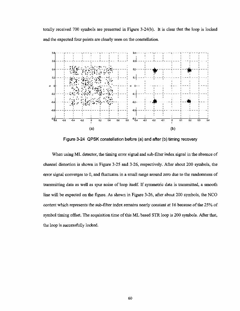
totally received 700 symbols are presented in Figure 3-24(b). It is clear that the loop is locked
and the expected four points are clearly seen on the constellation.
0.8
02
o 0
•02
-0.4-
•0.6
! ! ! ! T T j I I I I I I I
1 I I I L J. 1
,_ _ j ^ ju :, - : -;-,._:_,-% . _ - y £ - - r — i . . j-.v U-. » • ! • i • , i ; i . ' s i . • i
I I • • • • •! * . . l \ • • ! • I I
- - - - - - - V ' j ' - H ^ ' - ^ 7 ... - - - V - -
I > I • *l " • I . . .J . • . • • • ! • I
L - ' ^ ..- £T-1.*.*-! v~ v*.- *• H**-:- - •- — i i i i i i i i i i i i i i 1 1 1 1 T T 1
~ l
• - > - -
1
1
--M--t i
i
i 1
i 1
i i * i
—| — r — - j - — i — i i i i i i i i
— - — - - - * t — - — i i i t
"i T T r
i i i i
-0.6 -0.4 -0.2
0.3
02
0.1
o 0
-0.1
•02
•0.3
02 0.4 0.6 0.8 4.4 -0.3 -02 -0.1 0 0.1 02 0.3 0.4
(a) (b)
Figure 3-24 QPSK constellation before (a) and after (b) timing recovery
When using ML detector, the timing error signal and sub-filter index signal in the absence of
channel distortion is shown in Figure 3-25 and 3-26, respectively. After about 200 symbols, the
error signal converges to 0, and fluctuates in a small range around zero due to the randomness of
transmitting data as well as spur noise of loop itself. If symmetric data is transmitted, a smooth
line will be expected on the figure. As shown in Figure 3-26, after about 200 symbols, the NCO
content which represents the sub-filter index remains nearly constant at 16 because of the 25% of
symbol timing offset. The acquisition time of this ML based STR loop is 200 symbols. After that,
the loop is successfully locked.
60
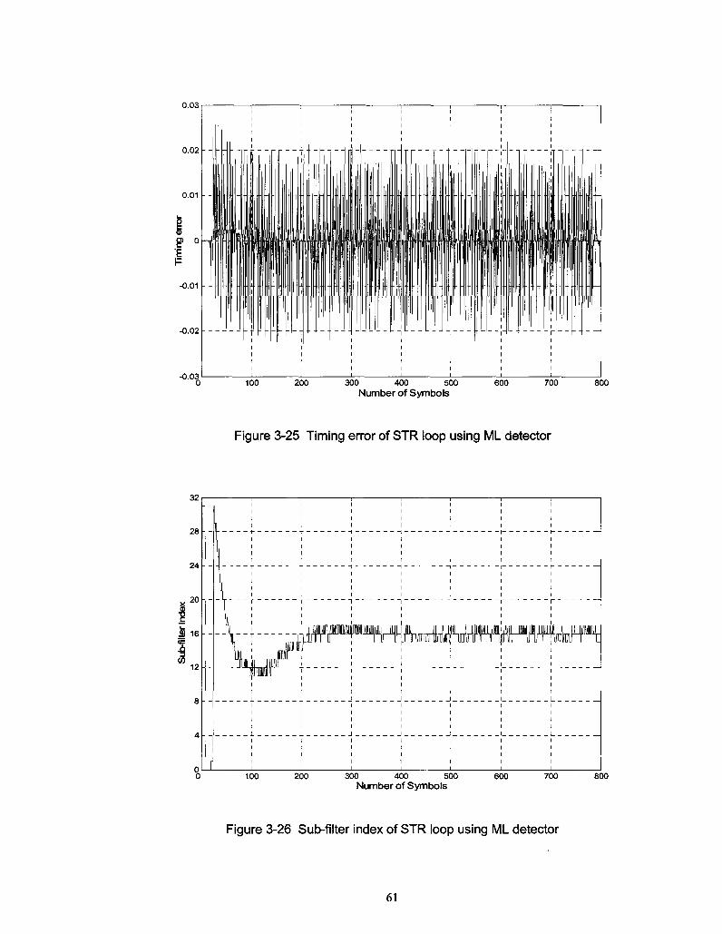
0.03
300 400 500 Number of Symbols
800
Figure 3-25 Timing error of STR loop using ML detector
32
28
24
20
16
i 12
]
[
I I ! I I I I
S i ! ! ! ! t i l l ! i \ I l ™ ^ IL-H jfflf"^^
i i i i i i i
i i i i i i i i i i i i i i
100 200 300 400 500
Number of Symbols 600 700 800
Figure 3-26 Sub-filter index of STR loop using ML detector
61
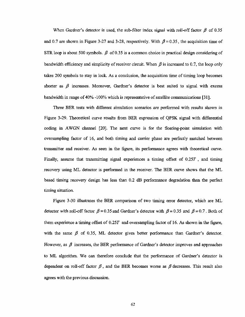
When Gardner's detector is used, the sub-filter index signal with roll-off factor J3 of 0.35
and 0.7 are shown in Figure 3-27 and 3-28, respectively. With /? = 0.35, the acquisition time of
STR loop is about 500 symbols. P of 0.35 is a common choice in practical design considering of
bandwidth efficiency and simplicity of receiver circuit. When (5 is increased to 0.7, the loop only
takes 200 symbols to stay in lock. As a conclusion, the acquisition time of timing loop becomes
shorter as f3 increases. Moreover, Gardner's detector is best suited to signal with excess
bandwidth in range of 40% -100% which is representative of satellite communications [31].
Three BER tests with different simulation scenarios are performed with results shown in
Figure 3-29. Theoretical curve results from BER expression of QPSK signal with differential
coding in AWGN channel [20]. The next curve is for the floating-point simulation with
oversampling factor of 16, and both timing and carrier phase are perfectly matched between
transmitter and receiver. As seen in the figure, its performance agrees with theoretical curve.
Finally, assume that transmitting signal experiences a timing offset of 0.2577 , and timing
recovery using ML detector is performed in the receiver. The BER curve shows that the ML
based timing recovery design has less than 0.2 dB performance degradation than the perfect
timing situation.
Figure 3-30 illustrates the BER comparison of two timing error detector, which are ML
detector with roll-off factor /3 = 0.35 and Gardner's detector with /? = 0.35 and J3 = 0.7. Both of
them experience a timing offset of 0.25T and oversampling factor of 16. As shown in the figure,
with the same f5 of 0.35, ML detector gives better performance than Gardner's detector.
However, as /5 increases, the BER performance of Gardner's detector improves and approaches
to ML algorithm. We can therefore conclude that the performance of Gardner's detector is
dependent on roll-off factor P, and the BER becomes worse as /? decreases. This result also
agrees with the previous discussion.
62
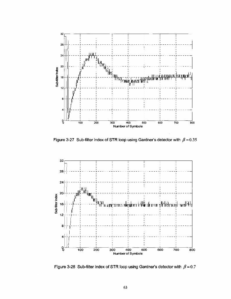
W
300 400 500 Number of Symbols
800
Figure 3-27 Sub-filter index of STR loop using Gardner's detector with fi = 0.35
32
28
24
20
J| 16
I 12
%
-
I I I I I I I I I I I I I I
I I I I I I I
L
L
=
1 1 -J
r -r i
r r i
j ! j i i u ju i i i i u j rininijUMUu uwii|iu ut i i l i ra lynu wiuu m i i ny i
J 1 1 1 1 1 1 1
l 1 i 1 1 1 1 1
100 200 300 400 500 Number of Symbols
600 700 800
Figure 3-28 Sub-filter index of STR loop using Gardner's detector with ft = 0.7
63
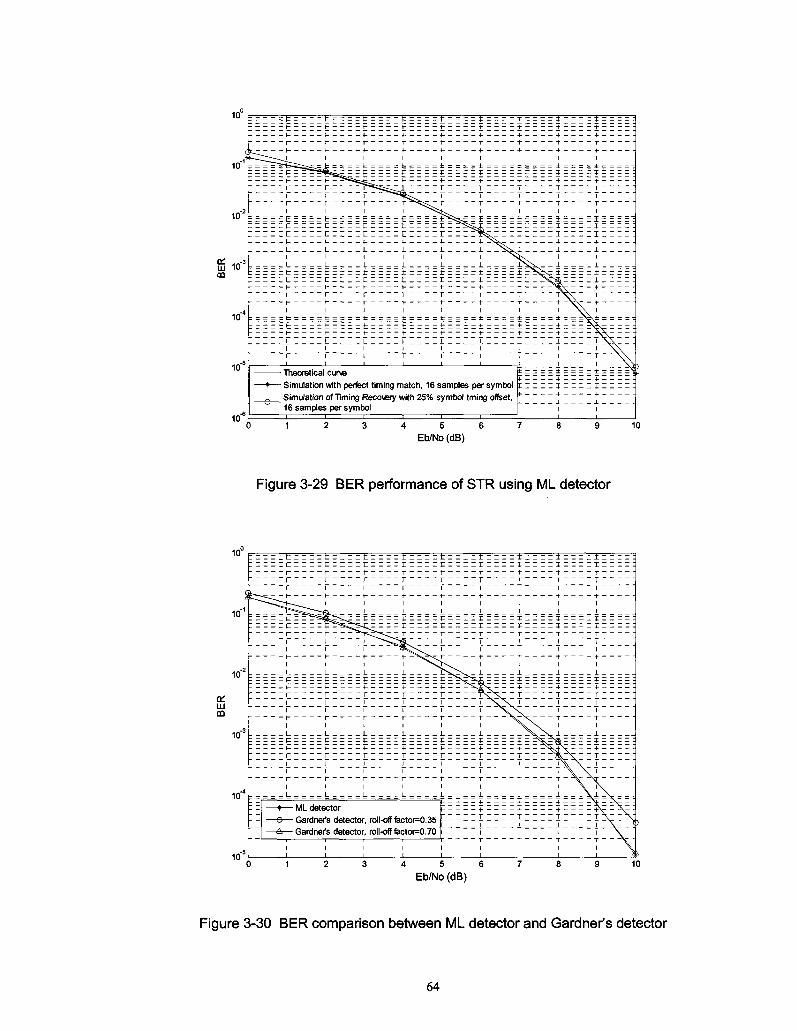
10
10
10 -.-
E io-3
CO
10
10
10
z - - - ^ ^ - - - - t - ~ ~ - - t - - ~ - t - ^ - - - t - - - ~ - V - ~ ~ - ' ^ ~ - - - ' t -I , , 1 i 1 ^ -r _
= = r t ~ - - - : 1-
r p ^ - = = s s ^ _ - ^ _ | j r _ _ r _ T T T _
+ T
I I I ^""^fet-- I I I I I
I I I I ^ ^ t - ^ ' ' ' i = = = = c = = = = c = = = = n = = = = c = = = = E = ^ ^ = ^ = = = = r = = = = ; r =
: - c n _ c E r _ ^ ^ r - J-L L L L I I ^ N . 1 1 —
11+ 114-
114
114-
114-
111
1 1 1 1 1 1 1 1 = t= fc fc fc fc £ fc ± ~
i \ j i H ^ H (._
: _ i :
i
_ !s\ I — ^vK
i I i i i i i i i \ X
I I I I I I I I I \ \
Simulation of Timing Recovery with 25% symbol tming offset, ^ 16 samples per symbol
t ± -i + -L 4-I 4 -
± ^ + j .
| 4 5 6
Eb/No (dB) 10
Figure 3-29 BER performance of STR using ML detector
10
10
10
00
10"-
10 ;
10
III 4-1 W
4-1 Ul
1 1 1 LIU
III
1 1 1
HI
44
H
4-1 l-l
4-IU : - - ± ± :
1 1 1 1 1 1 1 1 1
1 II
1 II
1 II
-4-
IK
1 II
- 4. _
-IUI
1 II
1 H
1 | ! ^ H i = ^ ^ - 4-
1 1 1 H + • - -
1 1 1
J 4- 4 4 4
1 1 1 ^ ^ " • ^ S ® - . 1 1 1 1 1 1 1 1 ^ ^ ^ > -
1 1 1 1 ^ " s ,
: c c c c
i + - -
S ^ \ ^ 1 1 c r ^ y S j . i _ :
- - - ; ; : _ _ T X :
+ 4.
1 1 1 1 1 1 ~ \ \ ^ 1 1 1
1 1 1 1
III 111 II II
1 114
III 1
ILL
II II II
1 IU
M
l
II 1
IU
III III
1 i t + .
i \ ~ \
J 1 l \ t : : - f - : : : r :
f 1- '
- - ^ i \ + 1 1 1 1 1 1 1 l^.~\. ' 1 1 1 1 1 1 1 1 ~ \ ~ \ 1
" ~ L L L L
— * — ML detector
—A— Gardner's detector, roll-off fector=0.70
i i i i
i i
J_ J. l _ | 4 +. _ . 1 H + .__
T T ~
1 X 1 X 1- \ ^ — —\- —
T T \ \ " 1 1 1 1 1 \ * 1 1 1 1 1 \
1 1 i i
1 ' \ 4 5 6
Eb/No (dB) 10
Figure 3-30 BER comparison between ML detector and Gardner's detector
64
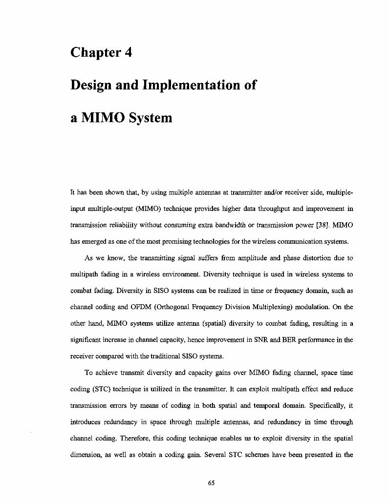
Chapter 4
Design and Implementation of
a MEMO System
It has been shown that, by using multiple antennas at transmitter and/or receiver side, multiple-
input multiple-output (MIMO) technique provides higher data throughput and improvement in
transmission reliability without consuming extra bandwidth or transmission power [38]. MIMO
has emerged as one of the most promising technologies for the wireless communication systems.
As we know, the transmitting signal suffers from amplitude and phase distortion due to
multipath fading in a wireless environment. Diversity technique is used in wireless systems to
combat fading. Diversity in SISO systems can be realized in time or frequency domain, such as
channel coding and OFDM (Orthogonal Frequency Division Multiplexing) modulation. On the
other hand, MIMO systems utilize antenna (spatial) diversity to combat fading, resulting in a
significant increase in channel capacity, hence improvement in SNR and BER performance in the
receiver compared with the traditional SISO systems.
To achieve transmit diversity and capacity gains over MIMO fading channel, space time
coding (STC) technique is utilized in the transmitter. It can exploit multipath effect and reduce
transmission errors by means of coding in both spatial and temporal domain. Specifically, it
introduces redundancy in space through multiple antennas, and redundancy in time through
channel coding. Therefore, this coding technique enables us to exploit diversity in the spatial
dimension, as well as obtain a coding gain. Several STC schemes have been presented in the
65
literature, including space-time block codes (STBC), space-time trellis codes (STTC), layered
space-time codes (LSTC) and some concatenated, unitary and differential space-time codes [38].
Alamouti scheme is the first but efficient example of STBC. It can achieve full diversity gain
with maximum-likelihood decoding (MLD) in a 2-transmitter 1-receiver system [37]. In this
chapter, we will explain the design and implementation of a 2x1 MIMO system using Alamouti
scheme.
4.1 Overview of a MIMO System Design
Figure 4-1 shows the general structure of the 2x1 MIMO system based on our design. In the
transmitter side, the binary source is first differentially encoded and modulated using QPSK
scheme. The generated QPSK symbols are fed into Alamouti encoder with output split into two
branches. The coded symbols go through a PSF, and are oversampled by a factor of 2. The PSF is
a 32-tap SQRC filter with roll-off factor of 0.35. The following interpolation filter and DUC
upsample the signal by a factor of 8, and translate it from baseband to an IF. The IF signal is then
converted to analog domain via a DAC for transmission through a multipath fading channel with
AWGN. The transmitter structure is almost the same as SISO system, except that two processing
branches are needed for the purpose of using two transmitters. In addition, we assume that there is
no frequency or phase offset between the two transmitter chains. Therefore, the local oscillators
of two transmitters share the same clock and generate the same carriers.
In the receiver side, an ADC first converts the received signal back to digital domain. The IF
signal is then down-converted to baseband and down-sampled by a decimation filter with a factor
of 8. Symbol timing recovery and carrier recovery are performed afterwards in order to track and
compensate the timing and carrier offset, respectively. The rest of the stages are ML decoding,
QPSK demodulation, and differential decoding. The channel state information (CSI) is assumed
to be known in the receiver, hence simplify the design. The receiver structure is also similar to
66
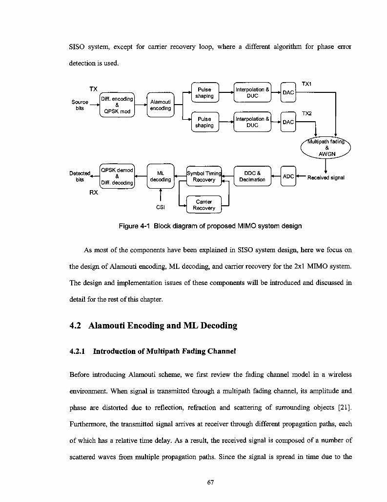
SISO system, except for carrier recovery loop, where a different algorithm for phase error
detection is used.
TX
Source bits
Diff. encoding &
QPSK mod
r > Alamouti encoding
V J
Pulse shaping
( ^ Pulse
shaping
TX1
Detected^ bits
QPSK demod &
Diff. decoding
ML decoding
RX
CSI
Symbol TimingL Recovery
Carrier Recovery
DDC& Decimation Received signal
Figure 4-1 Block diagram of proposed MIMO system design
As most of the components have been explained in SISO system design, here we focus on
the design of Alamouti encoding, ML decoding, and carrier recovery for the 2x1 MIMO system.
The design and implementation issues of these components will be introduced and discussed in
detail for the rest of this chapter.
4.2 Alamouti Encoding and ML Decoding
4.2.1 Introduction of Multipath Fading Channel
Before introducing Alamouti scheme, we first review the fading channel model in a wireless
environment. When signal is transmitted through a multipath fading channel, its amplitude and
phase are distorted due to reflection, refraction and scattering of surrounding objects [21].
Furthermore, the transmitted signal arrives at receiver through different propagation paths, each
of which has a relative time delay. As a result, the received signal is composed of a number of
scattered waves from multiple propagation paths. Since the signal is spread in time due to the
67
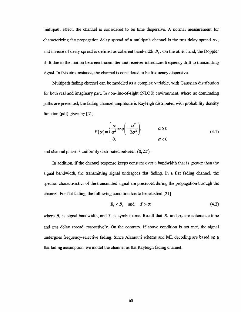
multipath effect, the channel is considered to be time dispersive. A normal measurement for
characterizing the propagation delay spread of a multipath channel is the rms delay spread ax,
and inverse of delay spread is defined as coherent bandwidth Bc. On the other hand, the Doppler
shift due to the motion between transmitter and receiver introduces frequency drift to transmitting
signal. In this circumstance, the channel is considered to be frequency dispersive.
Multipath fading channel can be modeled as a complex variable, with Gaussian distribution
for both real and imaginary part. In non-line-of-sight (NLOS) environment, where no dominating
paths are presented, the fading channel amplitude is Rayleigh distributed with probability density
function (pdf) given by [21]
f a 2 ^ P(or) =
a ^ e x p V 2s-2 J
or>0 (4.1)
0, « < 0
and channel phase is uniformly distributed between (0,2;r).
In addition, if the channel response keeps constant over a bandwidth that is greater than the
signal bandwidth, the transmitting signal undergoes flat fading. In a flat fading channel, the
spectral characteristics of the transmitted signal are preserved during the propagation through the
channel. For flat fading, the following condition has to be satisfied [21]
BS<BC and T>aT (4.2)
where Bs is signal bandwidth, and T is symbol time. Recall that Bc and <yT are coherence time
and rms delay spread, respectively. On the contrary, if above condition is not met, the signal
undergoes frequency-selective fading. Since Alamouti scheme and ML decoding are based on a
flat fading assumption, we model the channel as flat Rayleigh fading channel.
68

4.2.2 Introduction of Alamouti Scheme
Alamouti is a simple but efficient STBC scheme. It allows the transmission simultaneously from
two antennas with the same data rate as in a SISO system, but increases the transmit diversity
from one to two in a flat fading channel. Figure 4-2 illustrates a simplified 2x1 MIMO system
using Alamouti scheme. As shown in the figure, two consecutive symbols (xux2) are first fed
into encoder and sequence (xu-x2) and (x2,xl\ are then transmitted from antenna 1 and
antenna 2 respectively, during two consecutive symbol times, where x* denotes complex
conjugate of symbol x and T is symbol period. After that, the symbols are encoded both in space
and time domain, and the transmitting sequences from two antennas are orthogonal to each other.
Transmission period
t+T t Tx1
Symbol pair
( * 1 J *2 ) Alamouti encoder
*! ~ * 2 ;
* ! *1 i
j Xx
! X2
T 7x2
Y
Rx
Y-(r"r2) h.
-e-AWGN
(nx,n2)
ML decoder
& Channel estimator
\sXis2)
Figure 4-2 Alamouti encoding and ML decoding in a 2x1 MIMO system
Assume that the signal experiences a flat Rayleigh fading channel, and the channel response
keeps constant during 2 consecutive symbol times. So the received signal during these 2 symbol
periods is given by
rx = hxxi + h^x2 + "i
r2 = —l\x\ + hqx[ + «2
(4.3)
where hx and h^ are the fading channel response from two transmitter antennas, and^ , n2 are
independent complex additive noise with zero mean and power spectral density of N0/2 per
dimension. If the channel state information (CSI) is perfectly known at the receiver, maximum
69
likelihood decoding amounts to minimizing the following decision metric [38]
|?i - hiXi - h2x2 | + \r2 + hxx*2 - hix\ (4.4)
over all possible values of xx andx2 . The above function can be further decomposed into 2 parts
l*iI (W +\^2\ )~{r\h*xi +f\hxi +r2h2txl +r2*/j2x1*l
2 (4-5) IX2 f (|^l f +1^2f ) - (1*2*2 + 1**2*2 - *2*1**2 ~ *2**1*2 )
In expression (4.5), the upper part is only a function of xx, while the lower one is only a
function of x2 . As a conclusion, the 2x1 MIMO system is therefore decoupled into two
independent SISO channels, with channel gain of [Ih^ +\h2\ I. Furthermore, For M-PSK signals,
all the constellation points have equal energies, and the first item of Eq. (4.5) \x\ (\hx\ +|/^| lean
|
|2 *1 ~r\K _r2**2 tO
|
|2 *2 - 1*2 + r2**i to decode X2. Therefore, the ML decoding for
MPSK signal can be expressed as searching for the closest symbol point to sx and s2 on the
constellation, where
sl=hlr[+h2r2
s2=h2rl -hxr2
For QPSK modulation, decoding sx and s2 can be further simplified by detecting their sign
and allocating them to according quadrant. In the section of simulation and analysis, we will
examine the performance of Alamouti scheme in a flat fading channel.
4.2.3 Design and Implementation
4.2.3.1 Alamouti Encoder
Let's denote the 2 consecutive QPSK symbol as x1=a + bj, x2=c + dj, respectively. Based on
the mapping scheme in figure 4-2, the encoded symbols transmitted via antenna 1 in two symbol
70
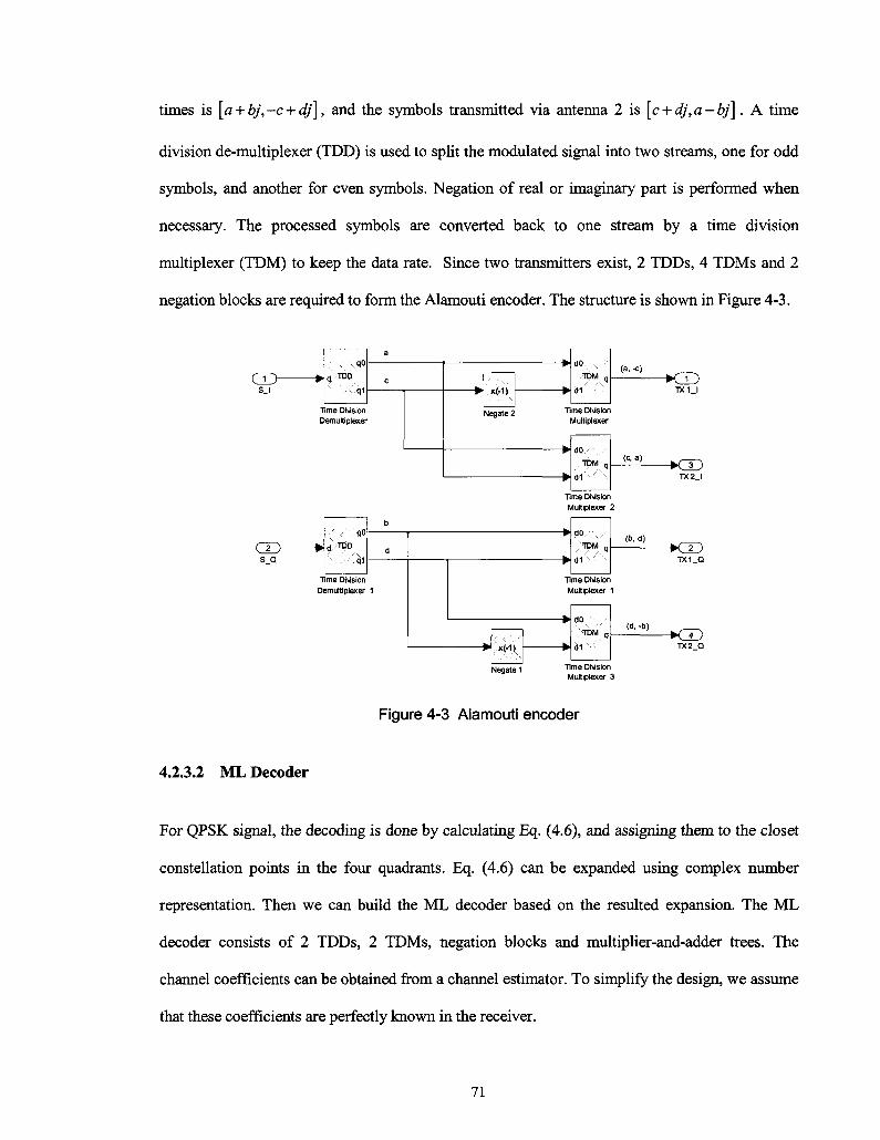
times is [a + bj,-c + dj], and the symbols transmitted via antenna 2 is [c + dj,a-bj]. A time
division de-multiplexer (TDD) is used to split the modulated signal into two streams, one for odd
symbols, and another for even symbols. Negation of real or imaginary part is performed when
necessary. The processed symbols are converted back to one stream by a time division
multiplexer (TDM) to keep the data rate. Since two transmitters exist, 2 TDDs, 4 TDMs and 2
negation blocks are required to form the Alamouti encoder. The structure is shown in Figure 4-3.
r 1 ^ s_i
7 c
q1
me Division emultiplexer
a
c x(-1)
Negate 2
dO TDM q
Time Diusion Multiplexer
dO - '•;./ TDM q
<H - < \
(a.-c)
(ca)
±r *{.
( 2 y-S Q
Time Diusion Multiplexer 2
,qO
d/TOD
Time Di\ision Demultiplexer 1
* d o : (b, d)
Time DiMSion Multiplexer 1
HdO.
x(-1) H<I1
(d. -b)
Negate 1 Time Dhrision Multiplexer 3
Figure 4-3 Alamouti encoder
4.2.3.2 ML Decoder
-KZ3
-KT>
For QPSK signal, the decoding is done by calculating Eq. (4.6), and assigning them to the closet
constellation points in the four quadrants. Eq. (4.6) can be expanded using complex number
representation. Then we can build the ML decoder based on the resulted expansion. The ML
decoder consists of 2 TDDs, 2 TDMs, negation blocks and multiplier-and-adder trees. The
channel coefficients can be obtained from a channel estimator. To simplify the design, we assume
that these coefficients are perfectly known in the receiver.
71
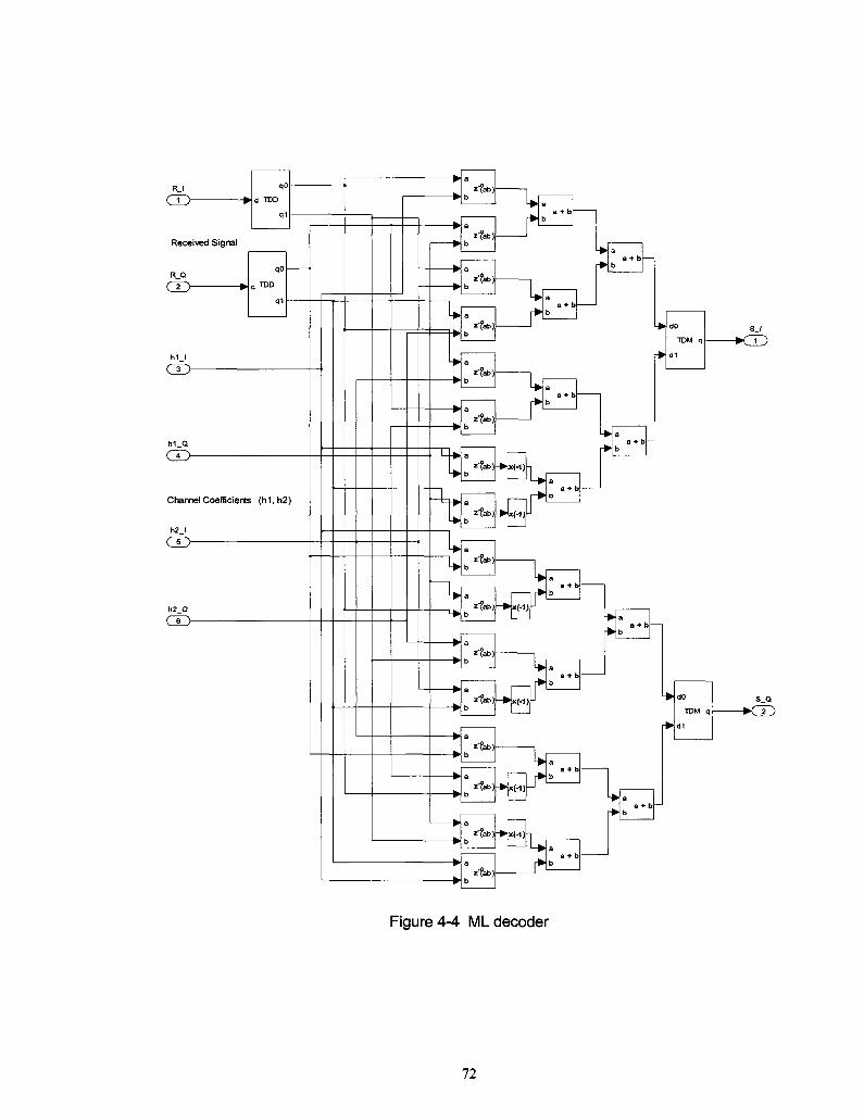
RJ
Received Signal
qO-
R_Q
d>
h1_l ( 3 y-
h1_Q
Channel Coefficients (h1,h2)
h2_l
(JD
h2_Q ( e y-
I i " fab)>x(-1) J
*1abf
•"M Mi
I'fab)
V '"fab)
TDM qf-
'•fab)
'"fab) J "
4ab) x(-1)
a a + b
b
u* fab)
lw ffab) R1>
'Tab)
cf 'Tab)
*7ab) x(-1)
4ab) x(-1)
lUt i tab)
a a + b
b
TDM qf-
a a + b
b
S_l - » ( 1 )
S_Q
-K5D
Figure 4-4 ML decoder
72
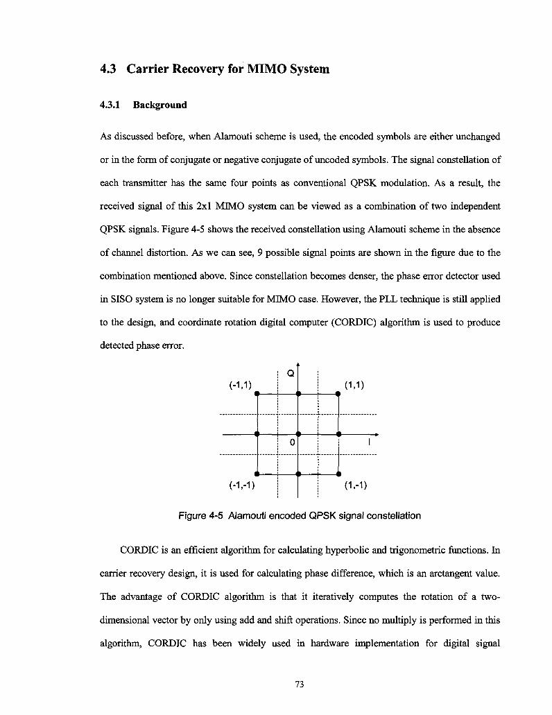
4.3 Carrier Recovery for MIMO System
4.3.1 Background
As discussed before, when Alamouti scheme is used, the encoded symbols are either unchanged
or in the form of conjugate or negative conjugate of uncoded symbols. The signal constellation of
each transmitter has the same four points as conventional QPSK modulation. As a result, the
received signal of this 2x1 MIMO system can be viewed as a combination of two independent
QPSK signals. Figure 4-5 shows the received constellation using Alamouti scheme in the absence
of channel distortion. As we can see, 9 possible signal points are shown in the figure due to the
combination mentioned above. Since constellation becomes denser, the phase error detector used
in SISO system is no longer suitable for MIMO case. However, the PLL technique is still applied
to the design, and coordinate rotation digital computer (CORDIC) algorithm is used to produce
detected phase error.
(-1.1) 1
1
1
(-1.-1)
i Q
1 1
t i i
: 0
i ' t
i i
i i
(1.1)
i
i
(1.-1)
Figure 4-5 Alamouti encoded QPSK signal constellation
CORDIC is an efficient algorithm for calculating hyperbolic and trigonometric functions. In
carrier recovery design, it is used for calculating phase difference, which is an arctangent value.
The advantage of CORDIC algorithm is that it iteratively computes the rotation of a two-
dimensional vector by only using add and shift operations. Since no multiply is performed in this
algorithm, CORDIC has been widely used in hardware implementation for digital signal
73
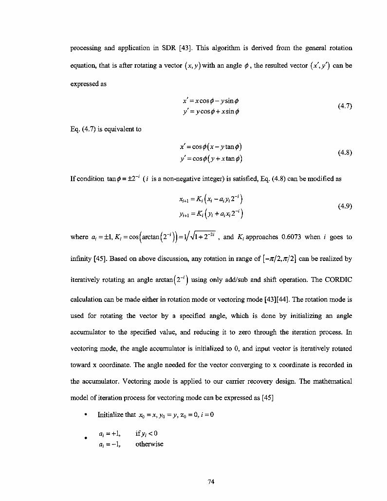
processing and application in SDR [43]. This algorithm is derived from the general rotation
equation, that is after rotating a vector (x,y) with an angle <f>, the resulted vector (x',y') can be
expressed as
x =xcosd) — ysm.0 (4.7)
y = j>cos0 + xsin0
Eq. (4.7) is equivalent to
x' = cos^fx - y tand>) , (4-8)
y '= cos0(.y + xtan^)
If condition tan <f> = ±2~' (i is a non-negative integer) is satisfied, Eq. (4.8) can be modified as
; ' (4-9) yM=Ki[yi + aixi2 ' )
where a, =±1, JT, =cos(arctan(2_i )j = l/Vl + 2_2i , and AT,-approaches 0.6073 when i goes to
infinity [45]. Based on above discussion, any rotation in range of \-KJ2,KJ2\ can be realized by
iteratively rotating an angle arctan(2-') using only add/sub and shift operation. The CORDIC
calculation can be made either in rotation mode or vectoring mode [43] [44]. The rotation mode is
used for rotating the vector by a specified angle, which is done by initializing an angle
accumulator to the specified value, and reducing it to zero through the iteration process. In
vectoring mode, the angle accumulator is initialized to 0, and input vector is iteratively rotated
toward x coordinate. The angle needed for the vector converging to x coordinate is recorded in
the accumulator. Vectoring mode is applied to our carrier recovery design. The mathematical
model of iteration process for vectoring mode can be expressed as [45]
• Initialize that JC0 = x, y0 = y, z0=0,i = 0
at = +1, if y{ < 0
at = - 1 , otherwise
74
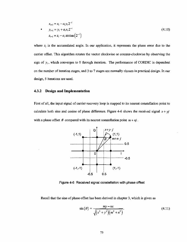
•"i'+l — Xi ~ aiyi 2
yM=yi+aixi2~' zi+\ = zt - at arctanf 2"' 1
(4.10)
where z, is the accumulated angle. In our application, it represents the phase error due to the
carrier offset. This algorithm rotates the vector clockwise or counter-clockwise by observing the
sign of v,-, which converges to 0 through iteration. The performance of CORDIC is dependent
on the number of iteration stages, and 3 to 7 stages are normally chosen in practical design. In our
design, 5 iterations are used.
4.3.2 Design and Implementation
First of all, the input signal of carrier recovery loop is mapped to its nearest constellation point to
calculate both sine and cosine of phase difference. Figure 4-6 shows the received signal x + yj
with a phase offset 6 compared with its nearest constellation point m + nj.
(-1.1) i
1
4
(-1.-1)
i Q
i o
;X+y
jr n . •j
. (1.1) ' m+n-j
I
(1.-1)
0.5
-0.5
-0.5 0.5
Figure 4-6 Received signal constellation with phase offset
Recall that the sine of phase offset has been derived in chapter 3, which is given as
sin (*) my-nx
J(x2+y2)(m>W)
(4.11)
75
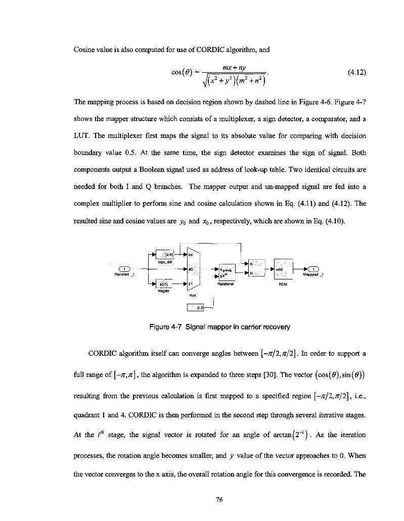
Cosine value is also computed for use of CORDIC algorithm, and
mx + ny cos (9)
^ 2+ / ) ( m 2
+ n 2 ) ' (4.12)
The mapping process is based on decision region shown by dashed line in Figure 4-6. Figure 4-7
shows the mapper structure which consists of a multiplexer, a sign detector, a comparator, and a
LUT. The multiplexer first maps the signal to its absolute value for comparing with decision
boundary value 0.5. At the same time, the sign detector examines the sign of signal. Both
components output a Boolean signal used as address of look-up table. Two identical circuits are
needed for both I and Q branches. The mapper output and un-mapped signal are fed into a
complex multiplier to perform sine and cosine calculation shown in Eq. (4.11) and (4.12). The
resulted sine and cosine values are y0 and x0, respectively, which are shown in Eq. (4.10).
^T~^ L_U Received 1
- * V0[a:b
sign del
}\— L>
-> x(-1)
Negate
sel
a i ^
mux
[<•'$ , H
aa<=b
*6\
—ta* hi -,"'\-"'
—• addr fciT^
*L±J Mappped I
Figure 4-7 Signal mapper in carrier recovery
CORDIC algorithm itself can converge angles between [-7r/2,n/2\. In order to support a
full range of \-n,7t\, the algorithm is expanded to three steps [30]. The vector (cos(0),sin(#))
resulting from the previous calculation is first mapped to a specified region [-;r/2,;r/2], i.e.,
quadrant 1 and 4. CORDIC is then performed in the second step through several iterative stages.
At the /'* stage, the signal vector is rotated for an angle of arctan(2~') . As the iteration
processes, the rotation angle becomes smaller, and v value of the vector approaches to 0. When
the vector converges to the x axis, the overall rotation angle for this convergence is recorded. The
76
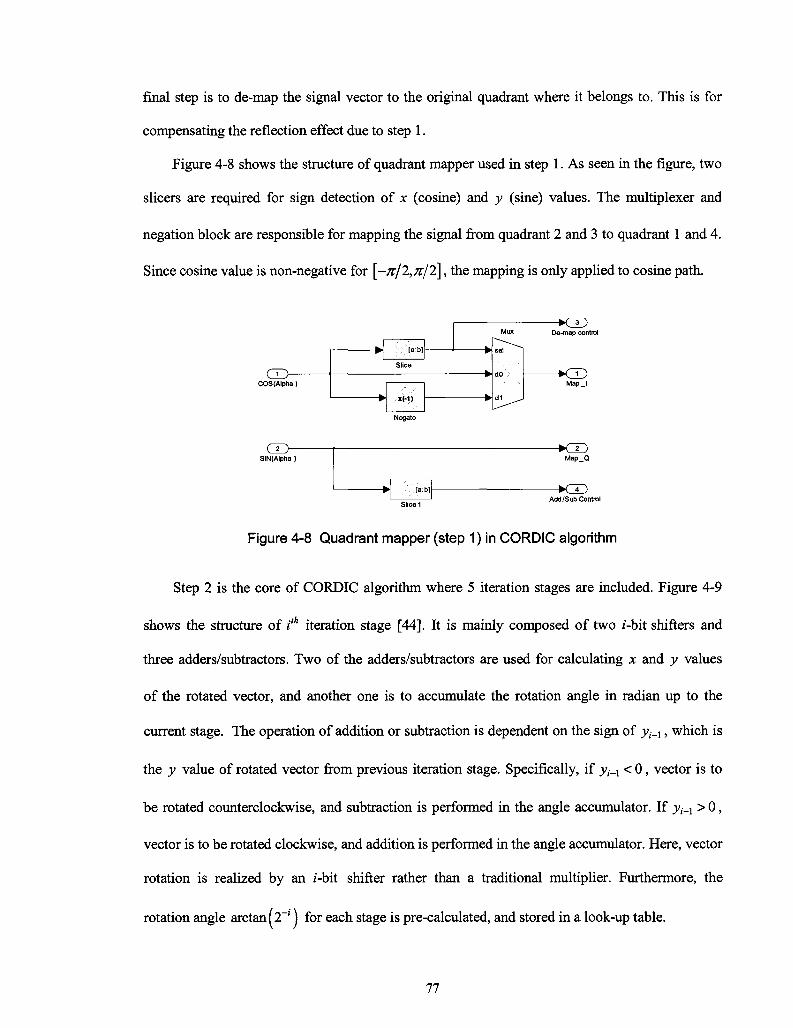
final step is to de-map the signal vector to the original quadrant where it belongs to. This is for
compensating the reflection effect due to step 1.
Figure 4-8 shows the structure of quadrant mapper used in step 1. As seen in the figure, two
slicers are required for sign detection of x (cosine) and y (sine) values. The multiplexer and
negation block are responsible for mapping the signal from quadrant 2 and 3 to quadrant 1 and 4.
Since cosine value is non-negative for [-7r/2,n/2], the mapping is only applied to cosine path.
r~r^\ LJ_J
r - ^ L_£_J SIN (Alpha )
U>>:b]
Slice
x(-1)
Negate
Mux
sel
dO )
d1 ^
De-map control
fcfl-^ *KJLJ
Map_Q
Add /Sub Control
Figure 4-8 Quadrant mapper (step 1) in CORDIC algorithm
Step 2 is the core of CORDIC algorithm where 5 iteration stages are included. Figure 4-9
shows the structure of /"" iteration stage [44]. It is mainly composed of two /-bit shifters and
three adders/subtractors. Two of the adders/subtractors are used for calculating x and y values
of the rotated vector, and another one is to accumulate the rotation angle in radian up to the
current stage. The operation of addition or subtraction is dependent on the sign of _yM, which is
the v value of rotated vector from previous iteration stage. Specifically, if y,_i < 0 , vector is to
be rotated counterclockwise, and subtraction is performed in the angle accumulator. If y^ > 0,
vector is to be rotated clockwise, and addition is performed in the angle accumulator. Here, vector
rotation is realized by an /-bit shifter rather than a traditional multiplier. Furthermore, the
rotation angle arctan(2"') for each stage is pre-calculated, and stored in a look-up table.
77
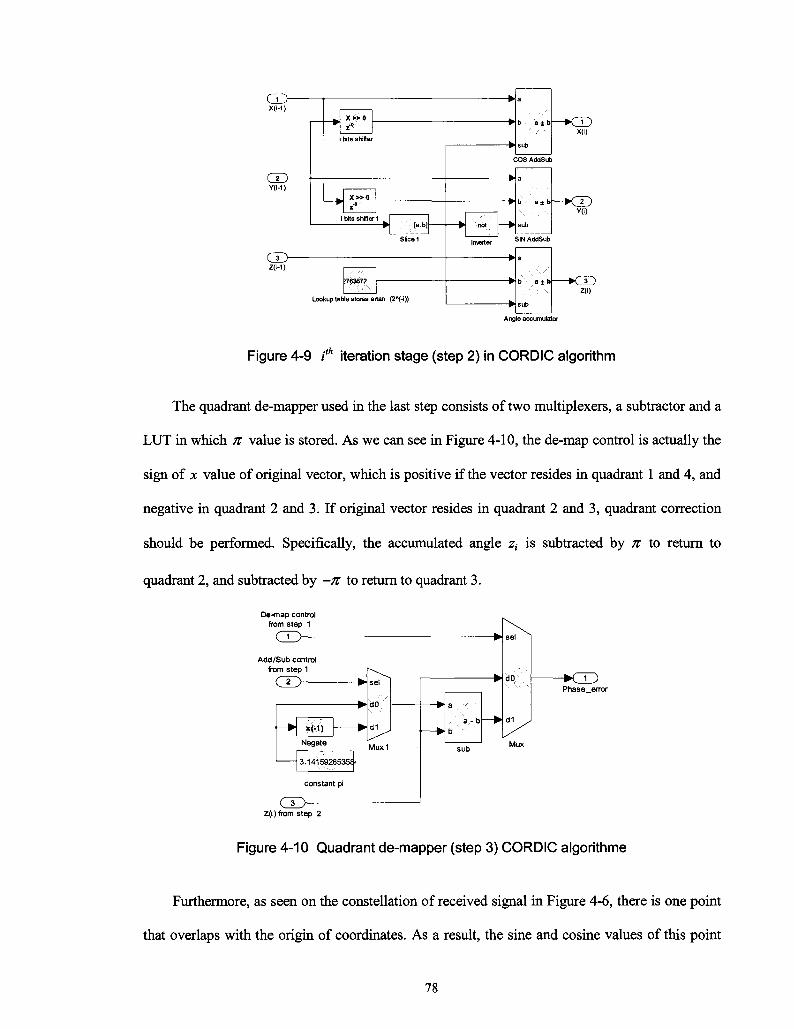
fT"1 X(i-1)
r~r I 2 > YO-1)
rv> Z(l-1)
i
X » > 0
aits shifter
X » 0
bits shifter 1 ; Ea:b]
Slice 1
763872
Lookup table stores aitan (2A(-i))
a
b a ± b
Sift)
COS AddSub
not
Inverter
- •
a
b a ± b
sub
SIN AddSub
a
b a ± b
sub
X(i)
Y(i)
Z(i)
Angle accumulator
Figure 4-9 i'h iteration stage (step 2) in CORDIC algorithm
The quadrant de-mapper used in the last step consists of two multiplexers, a subtracter and a
LUT in which n value is stored. As we can see in Figure 4-10, the de-map control is actually the
sign of x value of original vector, which is positive if the vector resides in quadrant 1 and 4, and
negative in quadrant 2 and 3. If original vector resides in quadrant 2 and 3, quadrant correction
should be performed. Specifically, the accumulated angle z, is subtracted by n to return to
quadrant 2, and subtracted by -n to return to quadrant 3.
De-mapc
from ste
GZ Add/Sub c
from ste
ontrol
P 1
J
ontrol
p1 •N h i J *
— •
d Z(i)trom
xfril) h i
3.14159265358
constant pi
step 2
set
dp
d1
^^ Mux1
a - b
b
— •
sel
dq,x
d1 ,
M U X
i , r n Phase enor
Figure 4-10 Quadrant de-mapper (step 3) CORDIC algorithme
Furthermore, as seen on the constellation of received signal in Figure 4-6, there is one point
that overlaps with the origin of coordinates. As a result, the sine and cosine values of this point
78
run to infinity. In this case, the received signal located in the decision region of this point should
not be processed to phase error detection in order to prevent the self-error of the algorithm. In
addition, phase ambiguity problem can be solved by differential encoding.
The output of CORDIC block is the detected phase error, which is then fed to loop filter and
NCO to accomplish phase adjustment. The design and implementation issue of loop filter and
NCO has been discussed in detail in SISO system design. Since theses components in our MIMO
system have same structure and specification, they are not emphasized here.
4.3.3 Simulation and Analysis
The carrier recovery of MIMO system is simulated using both system generator blocks and
Simulink blocks. The loop performance is analyzed by observing the constellation plot and phase
error signal. The BER performance in AWGN channel is also given. The simulation is based on
the following specifications.
• Modulation scheme: QPSK with differential coding
• Oversampling rate: 16
• Roll-off factor: 0.35
• Channel: Flat Rayleigh fading channel, AWGN
• Normalized frequency offset: 0.001 Hz
• Loop bandwidth: 0.1% normalized to symbol rate.
We first consider the case that receiver carrier is perfectly coherent with transmitter carrier,
and a simulation of 2x1 MIMO system using Alamouti scheme is performed. The BER
performance is shown in Figure 4-11. In a flat Rayleigh fading channel, where the channel
response keeps constant for every 2 symbols, the Alamouti scheme with QPSK modulation
performs much better than conventional SISO channel when CSI is known at the receiver. It
needs about 10 dB SNR less than SISO to obtain a BER of 10"3. However, two systems have the
same BER over AWGN channel, where the channel response keeps constant all the time.
79
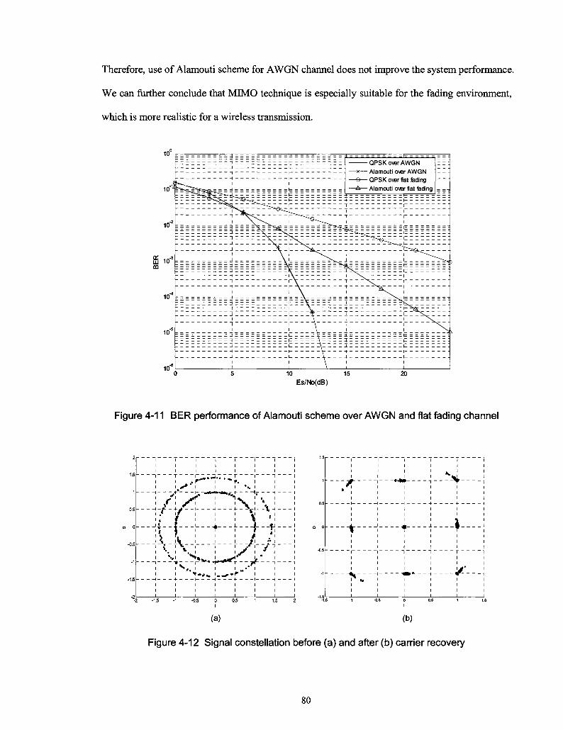
Therefore, use of Alamouti scheme for AWGN channel does not improve the system performance.
We can further conclude that MIMO technique is especially suitable for the fading environment,
which is more realistic for a wireless transmission.
10 QPSK over AWGN
—*— Alamouti over AWGN - e — QPSK over flat fading -A— Alamouti over flat fading
10 15 Es/No(dB)
Figure 4-11 BER performance of Alamouti scheme over AWGN and flat fading channel
2 -1
I I I I I I I
_J_ _ 4 y - - 1 1 1- _ 3^.1- - \ 4 1
i-|-;4-l-4-ii-! \ _ A - -L - - J - - - i. - _/'- -:•.!___) f- ! * 1 ! \s\ * \ \ --H- V x . ' - . J t * ' '
i * » i I i • " i I I
; _ _ J*-** _|«-r*f ; \ ] i i < i i i i i i i i i i i
5 -1 -0.5 0 0.5 1 1.5 2
-----jt----
—-i- — i
— - * — 1 »#
i i i i i i
^ _[ ^
i i i i i i l
— ^ . — - I — i « " — 1 i ! 1 1 1
-1 -0.5
(a) (b)
Figure 4-12 Signal constellation before (a) and after (b) carrier recovery
80
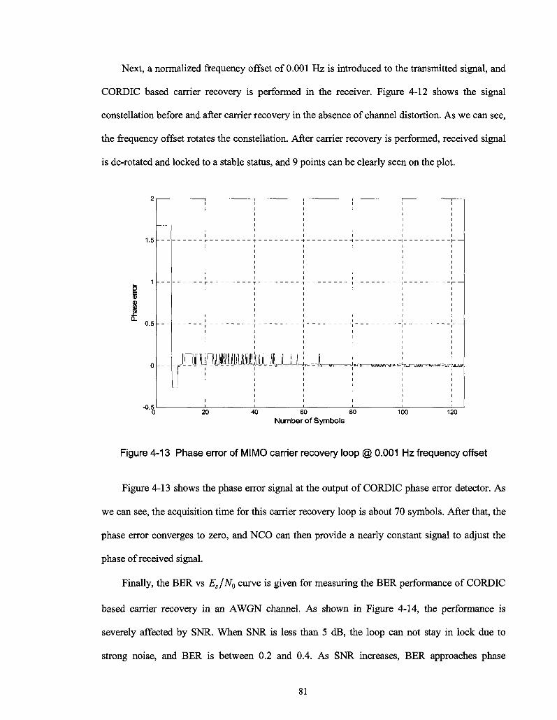
Next, a normalized frequency offset of 0.001 Hz is introduced to the transmitted signal, and
CORDIC based carrier recovery is performed in the receiver. Figure 4-12 shows the signal
constellation before and after carrier recovery in the absence of channel distortion. As we can see,
the frequency offset rotates the constellation. After carrier recovery is performed, received signal
is de-rotated and locked to a stable status, and 9 points can be clearly seen on the plot.
1.5
0.5
-0.5 0
iritiiM
20 40 60 80 Number of Symbols
100 120
Figure 4-13 Phase error of MIMO carrier recovery loop @ 0.001 Hz frequency offset
Figure 4-13 shows the phase error signal at the output of CORDIC phase error detector. As
we can see, the acquisition time for this carrier recovery loop is about 70 symbols. After that, the
phase error converges to zero, and NCO can then provide a nearly constant signal to adjust the
phase of received signal.
Finally, the BER vs Es/N0 curve is given for measuring the BER performance of CORDIC
based carrier recovery in an AWGN channel. As shown in Figure 4-14, the performance is
severely affected by SNR. When SNR is less than 5 dB, the loop can not stay in lock due to
strong noise, and BER is between 0.2 and 0.4. As SNR increases, BER approaches phase
81
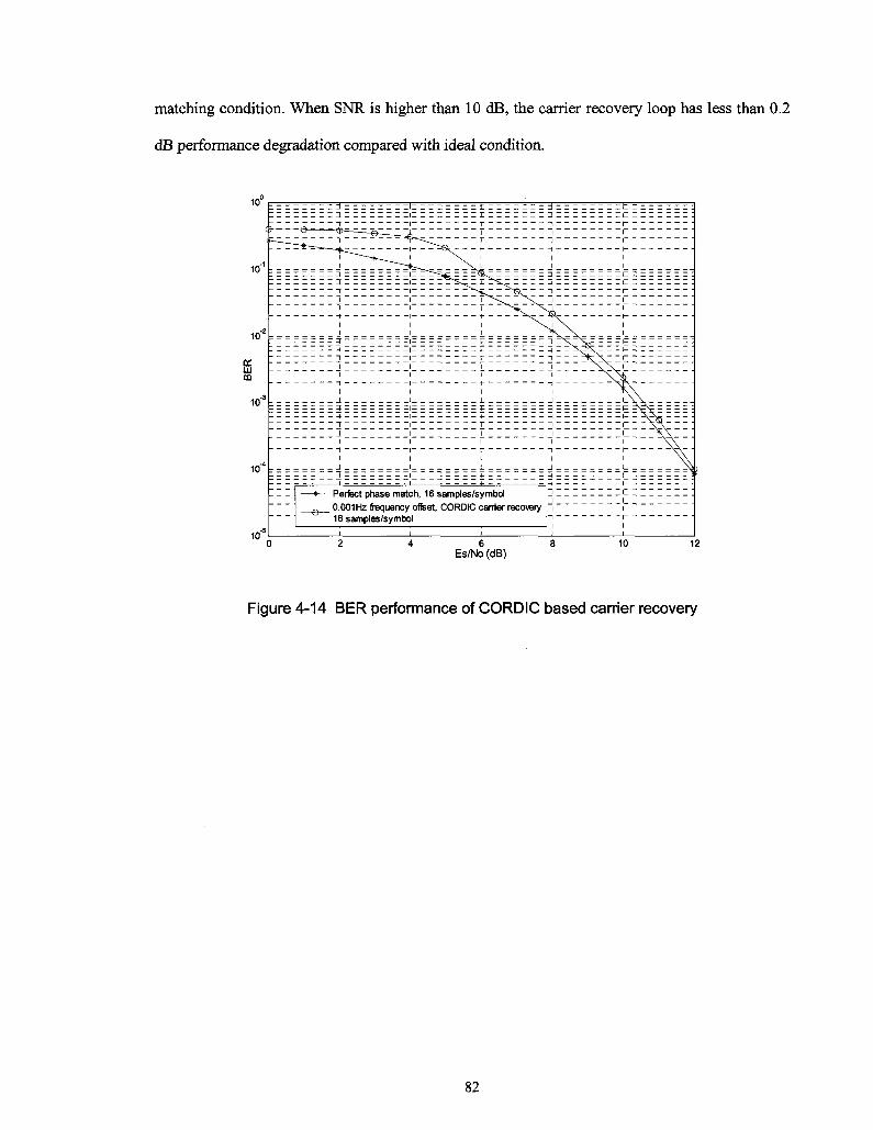
matching condition. When SNR is higher than 10 dB, the carrier recovery loop has less than 0.2
dB performance degradation compared with ideal condition.
10
10
10
UJ m
10
10
10
i 1 t d 1 •
7~~——~-*-__ ' ~*ir~~~~~"~~~~-^ ' ' '
l 1 1 ^ ^ . ^ v 1 1
1 i 1 ^K \ j i '
1 1 1 ^ r v \ 1 E 3 i - c q \ \ ^ i 3
i i i t \ \ i
1 1 1 1 ^^v^;
1 1 H 1 |_ - AS_
i i i i i XA 1 1 1 1 1 \ \
i—i
i—i
i i
i—
1. 1 i 1 i 3
: : : 1 | A 1 i .
— * — Perfect phase match, 16 samples/symbol
Q 0.001Hz frequency offset, CORDIC carrier reco\ery 16 samples/symbol
i i i
~i i i i i i
~i i
Es/No (dB) 10 12
Figure 4-14 BER performance of CORDIC based carrier recovery
82
Chapter 5
Hardware Description and Test Results
In chapter 2 & 3, we talked about the design and implementation issues of an SDR based SISO
system. After modeling using System Generator, and synthesizing and implementing the design
using ISE software, a bitstream performing low-level execution of high-level abstraction is
generated, and then downloaded to target FPGA. We can thus realize the design on hardware and
test its performance. In this chapter, the experimental platform and other test equipment are first
introduced. The test results of our SISO system design are then given and analyzed.
5.1 Introduction of Test Equipment
5.1.1 XtremeDSP Board
The testbed on which we implement the design is Nallatech XtremeDSP board. It is a
development platform providing FPGA technology, as well as high performance DACs and
ADCs. The board mainly contains three Xilinx's FPGAs, which are [49]
• A Virtex-4 user FPGA used as the main part of the design.
• A Virtex-2 clock FPGA for clock management. It controls and routes the clock to different
components on the board.
• A Spartan-II interface FPGA which is responsible for interface control between FPGAs, or
board and PC through USB/PCI interface.
83
The XtremeDSP board provides two ADCs with resolution of 14 bits and maximum
sampling frequency of 105 MHz, and two 14-bit DACs with sampling frequency of 160 MHz.
The DAC also features [49]:
• A half band symmetric interpolation filter with oversampling factor of 2.
It can be configured for low pass or high pass response. With low pass response, the
interpolation filter works at 2 times the input data rate to DAC, and significantly reduce the
magnitude of the first spectrum image of original signal. In our application, the first image of
the up-converted signal is moved from 75 MHz to 175 MHz by interpolation filtering. The
images centered at multiple of sampling rate because of sampling theory will be further
attenuated by the DACs siD.(x)/x response.
• A PLL clock multiplier that can provides synchronous clock for edge trigger latches,
interpolation filter and DAC.
On the other hand, the ADC also features:
• An anti-aliasing filter with cutoff frequency of 58 MHz, which can successfully exact high
frequency component for our application.
Furthermore, 4 clock resources are available for the board, which are:
• An on board fixed oscillator of 105 MHz.
• A programmable oscillator working up to 120 MHz.
• A user-provided oscillator socket.
• An external clock input via MCX connector or some user pins.
In addition, the board has some other important features:
• PCI/USB interface used for communication between FPGAs and host PC
• JTAG chains used for hardware test and configuration
• Two banks of ZBT-SRAM used for data storage. Each bank has 16 MB capacity with
working frequency of 133 MHz.
84
Besides the sufficient hardware resources and configuration flexibility, the XtremeDSP platform
provides easy and fast transition from algorithm simulation to hardware verification when
combined with System Generator. This platform is therefore ideal for signal processing
application such as SDR, HDTV, and so on. It is also suitable for our SISO system
implementation.
5.1.2 FB100A BER Tester
The BER performance of the design is measured by Aeroflex FB100A BER test system [51]. The
BER tester can generate user defined word pattern and pseudo random binary sequence (PRBS)
with selectable length up to 223 - 1 . The operating bit rate ranges from DC to 100 Mbps. Both
internal clock and external clock are available for bit generation. In our application, an external
clock of 12.5 MHz is required to generate a PRBS with rate of 12.5 Mbps. During each
transmission block, the machine adds a certain number of preambles to the binary sequence.
These preambles are monitored in the received sequence. If they are correctly detected, the tester
is considered in synchronization. If not, the machine is considered out of sync.
Aside from ability to calculate BER, the tester also functions as an AWGN channel emulator,
which can add bandpass white Gaussian noise to carrier wave from 5 MHz to 2.4 GHz. The noise
power can be controlled by the desired carrier to noise ratio, and carrier signal power is tracked
and measured by the machine. During BER calculation, the tester can generate plot of BER vs
SNR automatically. In addition, the machine supports testing with various signal modes, such as
continuous, TDMA, and burst mode. Based on properties introduced above, FBI00A can satisfy
our application requirement, and ease the test process.
The other test equipment includes digital oscilloscope and spectrum analyzer.
85
5.2 Hardware Setup and Connection
After introducing the hardware properties, we now explain how these equipments are correctly
setup and connected to accomplish the implementation and testing. Figure 5-1 illustrates the
hardware connection and signal routing path. First of all, we use the programmable oscillator as
the clock resource, and set master clock as 100 MHz for XtremeDSP board. This choice also
makes it convenient to transfer the design to other clock frequency. In order to generate a binary
data with rate of 12.5 Mbps which is synchronous with master clock, the 100 MHz is divided by 8
to obtain a synchronous 12.5 MHz clock. This is done by Digital Clock Manager (DCM) of
Virtex-4 chip [48]. DCM provides a wide range of powerful clock management features. It also
performs on-board clock de-skewing and clock forwarding in our application. The DCM contains
a delay-locked loop (DLL), and clock distribution delays can be completely eliminated by de
skewing the DCM's output clock with respect to the input clock. In addition, DCM provides
precise frequency synthesis, which can realize synchronous frequency division and multiplication.
It also allows coarse and fine phase shifting compared with input clock [48]. In our design, the
generated 12.5 MHz clock is forwarded to a double data rate (DDR) register, and then taken out
of the board from a user pin to drive the PRBS generator (BER tester). The propagation delay of
master clock signal distributed throughout the whole FPGA is also eliminated due to the on board
de-skew feature of DCM.
Figure 5.1 illustrates the connection between FPGA and BER tester, along with the
numbered signal routing path. The PRBS length is chosen as 223 - 1 with distribution sufficiently
close to the ideal uniform distribution. The generated bits are fed into the XtremeDSP board
through a user pin (Figure 5-1-1), and the baseband signal processing and digital up-conversion
are performed using the FPGAs. After going through DAC, an analog signal of 25 MHz is
generated (Figure 5-1-2). It is then connected with the AWGN channel emulator (BER tester) via
75 ohm port. The bandpass noise with bandwidth of approximately 8.37 MHz centered at 25
86
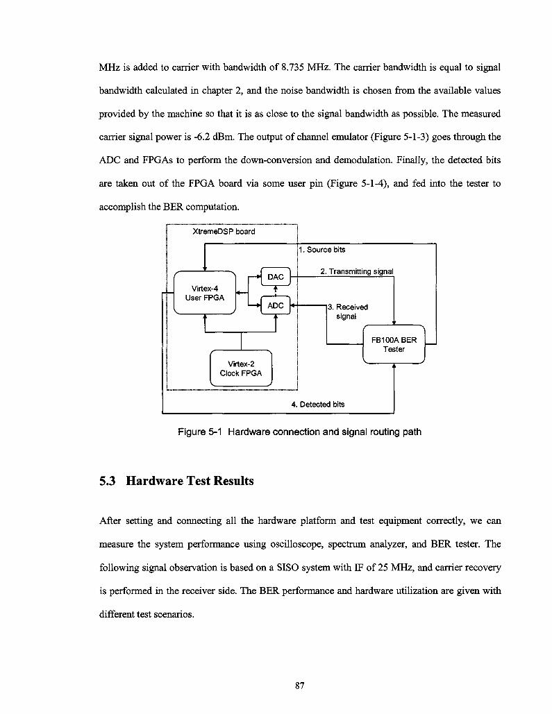
MHz is added to carrier with bandwidth of 8.735 MHz. The carrier bandwidth is equal to signal
bandwidth calculated in chapter 2, and the noise bandwidth is chosen from the available values
provided by the machine so that it is as close to the signal bandwidth as possible. The measured
carrier signal power is -6.2 dBm. The output of channel emulator (Figure 5-1-3) goes through the
ADC and FPGAs to perform the down-conversion and demodulation. Finally, the detected bits
are taken out of the FPGA board via some user pin (Figure 5-1-4), and fed into the tester to
accomplish the BER computation.
XtremeDSP board
( > Virtex-4
User FPGA
^ J <
„ •
DAC
+ •
ADC
C \ Virtex-2
Clock FPGA v J
i L
4.
1. Source bits
3. Received signal ' -
f "\ FB100ABER
Tester
t k
Detecte d bits
Figure 5-1 Hardware connection and signal routing path
5.3 Hardware Test Results
After setting and connecting all the hardware platform and test equipment correctly, we can
measure the system performance using oscilloscope, spectrum analyzer, and BER tester. The
following signal observation is based on a SISO system with IF of 25 MHz, and carrier recovery
is performed in the receiver side. The BER performance and hardware utilization are given with
different test scenarios.
87
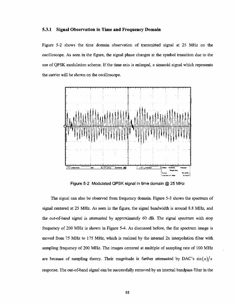
5.3.1 Signal Observation in Time and Frequency Domain
Figure 5-2 shows the time domain observation of transmitted signal at 25 MHz on the
oscilloscope. As seen in the figure, the signal phase changes at the symbol transition due to the
use of QPSK modulation scheme. If the time axis is enlarged, a sinusoid signal which represents
the carrier will be shown on the oscilloscope.
200fiB 10.0GS/B 10QpsJpt
Sin BID Soq
0 acqs RL;20.0V
Fobruarv 11. 2009 15:16:4
Figure 5-2 Modulated QPSK signal in time domain @ 25 MHz
The signal can also be observed from frequency domain. Figure 5-3 shows the spectrum of
signal centered at 25 MHz. As seen in the figure, the signal bandwidth is around 8.8 MHz, and
the out-of-band signal is attenuated by approximately 60 dB. The signal spectrum with stop
frequency of 200 MHz is shown in Figure 5-4. As discussed before, the fist spectrum image is
moved from 75 MHz to 175 MHz, which is realized by the internal 2x interpolation filter with
sampling frequency of 200 MHz. The images centered at multiple of sampling rate of 100 MHz
are because of sampling theory. Their magnitude is further attenuated by DAC's sin(x)/x
response. The out-of-band signal can be successfully removed by an internal bandpass filter in the
88
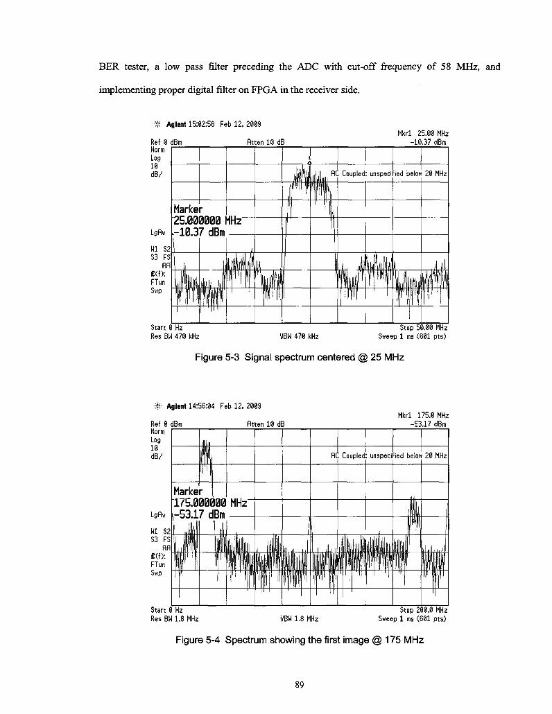
BER tester, a low pass filter preceding the ADC with cut-off frequency of 58 MHz, and
implementing proper digital filter on FPGA in the receiver side.
« Agilent 15:82:56 Feb 12, 2009
Ref 0 dBm fitten 10 dB Norm Log 10 dB/
Mkrl 25.00 MHz -10.37 dBm
Lgflv
HI S2 S3 FS
Rfl £( f ) : FTun Swp
Msrksr 25.000000 MHz~ -10.37 dBm
1 Start 0 Hz Res BW 470 kHz
RC Coupled: unspecified below 20 MHz
VBW 470 kHz Stop 50.00 MHz
Sweep 1 ms (601 pts)
Figure 5-3 Signal spectrum centered @ 25 MHz
* Agilent 14:56:04 Feb 12, 2009
Ref 0 dBm fltten 10 dB Norm Log 10 dB/
Mkrl 175.0 MHz -53.17 dBm
FlC Coupled: unspecified below 20 MHz
Lgflv
Wl S2 S3 FS
flfl £ ( f ) : FTun Swp
Msrker 175.000000 MHz -53.17 dBm
Start 0 Hz Res BH 1.8 MHz
Stop 200.0 MHz Sweep 1 ms (601 pts) VBW 1.8 MHz
Figure 5-4 Spectrum showing the first image @ 175 MHz
89
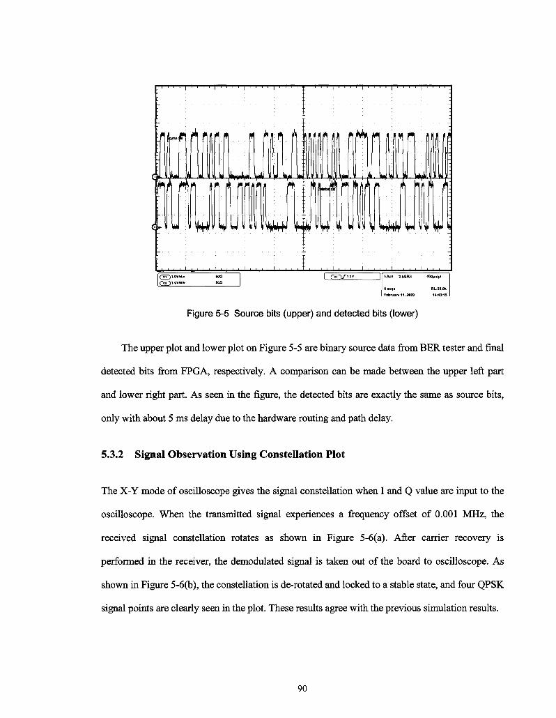
Figure 5-5 Source bits (upper) and detected bits (lower)
The upper plot and lower plot on Figure 5-5 are binary source data from BER tester and final
detected bits from FPGA, respectively. A comparison can be made between the upper left part
and lower right part. As seen in the figure, the detected bits are exactly the same as source bits,
only with about 5 ms delay due to the hardware routing and path delay.
5.3.2 Signal Observation Using Constellation Plot
The X-Y mode of oscilloscope gives the signal constellation when I and Q value are input to the
oscilloscope. When the transmitted signal experiences a frequency offset of 0.001 MHz, the
received signal constellation rotates as shown in Figure 5-6(a). After carrier recovery is
performed in the receiver, the demodulated signal is taken out of the board to oscilloscope. As
shown in Figure 5-6(b), the constellation is de-rotated and locked to a stable state, and four QPSK
signal points are clearly seen in the plot. These results agree with the previous simulation results.
90

$ — + .
.luavwf son |fo)lOOmV«v
i i i I I I I i i | i i i i | i i i i | i i i i | i i
1 i - v « " II
(a)
lOtyt n i V U SftBraJp
( > l I I • I I • I I I I • I I . I •
((jTJlOOmV.'Si
|(cT)100mWi»n
• J ' ' • H - « • • ' I * — H - . ) . ,
• ! • • • • • • . . . I . . . . I •
(b)
Run Staple
U ) H ) i Rl i lMt
FiDnmll .a iB 1S«:«i
Figure 5-6 Signal constellation before (a) and after (b) carrier recovery
5.3.3 BER Performance
The BER calculation is performed using BER tester. The BER vs Eb/N0 curves are given with
five different test points (Eb/N0 values). A total of 7.5xl09 bits were sent for every test point.
Figure 5-7 compares the BER performance between software simulation and hardware test of a
SISO system, where signal experiences frequency offset of 0.001 MHz and carrier recovery is
performed in the receiver. As seen in the figure, the hardware test shows approximately 1.2 dB
implementation loss compared with simulation result. Since a number of factors affect the
performance of a real hardware implementation rather than software simulation, such as
quantization noise, inaccuracy of AWGN bandwidth, self noise of equipment and so on, this 1.2
dB loss is considered as acceptable in a practical design. The BER comparison of a SISO system
with both carrier and timing recovery is shown in Figure 5-8, and a 25% symbol timing offset is
manually set between transmitter and receiver. As seen in the figure, when roll-off factor
/3 = 0.35, the ML detector has better performance than Gardner's detector. This also agrees with
the previous simulation results. The implementation loss is still 1.2 dB in this scenario.
91
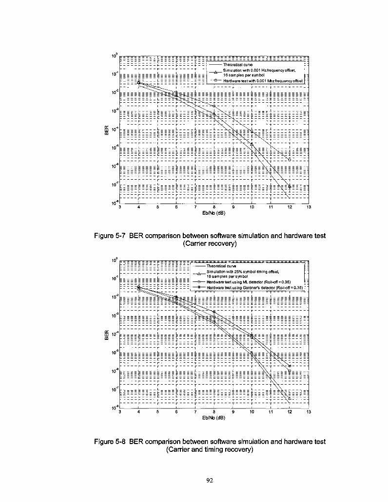
10 er
10
10%
10'
10
10'
10
10
10"
= - = = - E E = E E = = E -i , , 1
i i i i
= = = = = £ = = = = t ^ i T | ^ ^ § ^ ^ E E = =
— A -
° — 1 —
= = £ =
1 ( r^^^£^-^^ -= = = = = p = = = = C = = = = I= = = = = S = ^
z ^ "
£ = = = - £ ~i 5 = :
-Theoretical curve Simulation with 0.001 Hzfrequencyoffset, 16 samples per symbol Hardware testwith 0.001 Mizfrequency offset
!]
r r T T
= X = T = = = = ^ = = = = q: = = = = T= : = = = :
i i i i r -L L L i- L
z = = = = p= = = = = l= = = = = J= = = = = E = = := = J= = E C E E E E
L L L L L = = F F F £ F -z z c E n r E
r r r r r L L L L L
z E E E E E -
\ \ T > b \ T ~ T T
X ^ s : "igs- * T :
r rV X_ ~ i ^ . i q T T \ \ T T J- J- \ \ 1 E £ \ 2 X £ z ;
r r r r r r r - T \ -N. T
i i i i i
10 12 13
Eb/No (dB)
Figure 5-7 BER comparison between software simulation and hardware test (Carrier recovery)
10
10
10'
10'
10
10
10
: = f= = =
: = £ = = r m : * - - - = =~E~S : - * - - = = ± : - Theoretical curve
Simulation with 25% symbol timing offset, 16 samples persymbol
- Hardware test using twL detector (Roll-off = 0.35) - Hardware test using Gardner's detector (Roll-off = 0.35)
ffi 10 "U B . . .
10
10 11 12 13
Eb/No (dB)
Figure 5-8 BER comparison between software simulation and hardware test (Carrier and timing recovery)
92
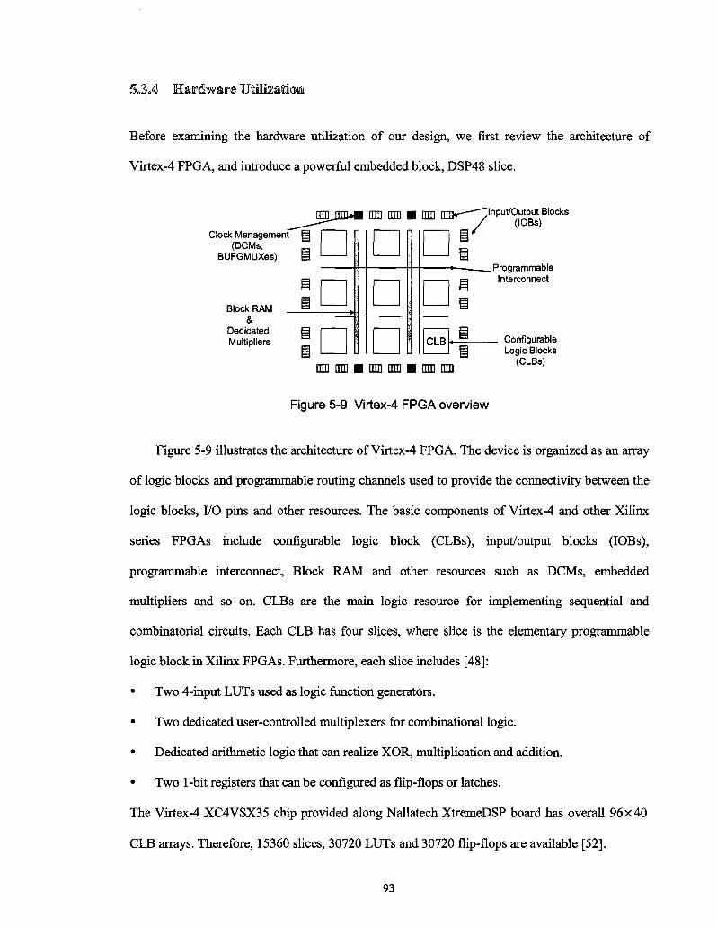
5.3.4 Hardware Utilization!
Before examining the hardware utilization of our design, we first review the architecture of
Virtex-4 FPGA, and introduce a powerful embedded block, DSP48 slice.
Clock Management (DCMs,
BUFGMUXes)
Block RAM &
Dedicated Multipliers
mss^m m m • am am*—-" input/output Blocks - ^ / (lOBs)
. Programmable Interconnect
CLBk- Configurable Logic Blocks
(CLBs) mn QUI • DID EUD • mn IHD
Figure 5-9 Virtex-4 FPGA overview
Figure 5-9 illustrates the architecture of Virtex-4 FPGA. The device is organized as an array
of logic blocks and programmable routing channels used to provide the connectivity between the
logic blocks, I/O pins and other resources. The basic components of Virtex-4 and other Xilinx
series FPGAs include configurable logic block (CLBs), input/output blocks (IOBs),
programmable interconnect, Block RAM and other resources such as DCMs, embedded
multipliers and so on. CLBs are the main logic resource for implementing sequential and
combinatorial circuits. Each CLB has four slices, where slice is the elementary programmable
logic block in Xilinx FPGAs. Furthermore, each slice includes [48]:
• Two 4-input LUTs used as logic function generators.
• Two dedicated user-controlled multiplexers for combinational logic.
• Dedicated arithmetic logic that can realize XOR, multiplication and addition.
• Two 1-bit registers that can be configured as flip-flops or latches.
The Virtex-4 XC4VSX35 chip provided along Nallatech XtremeDSP board has overall 96x40
CLB arrays. Therefore, 15360 slices, 30720 LUTs and 30720 flip-flops are available [52].
93
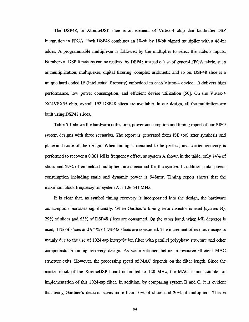
The DSP48, or XtremeDSP slice is an element of Virtex-4 chip that facilitates DSP
integration in FPGA. Each DSP48 combines an 18-bit by 18-bit signed multiplier with a 48-bit
adder. A programmable multiplexer is followed by the multiplier to select the adder's inputs.
Numbers of DSP functions can be realized by DSP48 instead of use of general FPGA fabric, such
as multiplication, multiplexer, digital filtering, complex arithmetic and so on. DSP48 slice is a
unique hard coded IP (Intellectual Property) embedded in each Virtex-4 device. It delivers high
performance, low power consumption, and efficient device utilization [50]. On the Virtex-4
XC4VSX35 chip, overall 192 DSP48 slices are available. In our design, all the multipliers are
built using DSP48 slices.
Table 5-1 shows the hardware utilization, power consumption and timing report of our SISO
system designs with three scenarios. The report is generated from ISE tool after synthesis and
place-and-route of the design. When timing is assumed to be perfect, and carrier recovery is
performed to recover a 0.001 MHz frequency offset, as system A shown in the table, only 14% of
slices and 29% of embedded multipliers are consumed for the system. In addition, total power
consumption including static and dynamic power is 948mw. Timing report shows that the
maximum clock frequency for system A is 126.541 MHz.
It is clear that, as symbol timing recovery is incorporated into the design, the hardware
consumption increases significantly. When Gardner's timing error detector is used (system B),
29% of slices and 63% of DSP48 slices are consumed. On the other hand, when ML detector is
used, 41% of slices and 94 % of DSP48 slices are consumed. The increment of resource usage is
mainly due to the use of 1024-tap interpolation filter with parallel polyphase structure and other
components in timing recovery design. As we mentioned before, a resource-efficient MAC
structure exits. However, the processing speed of MAC depends on the filter length. Since the
master clock of the XtremeDSP board is limited to 120 MHz, the MAC is not suitable for
implementation of this 1024-tap filter. In addition, by comparing system B and C, it is evident
that using Gardner's detector saves more than 10% of slices and 30% of multipliers. This is
94
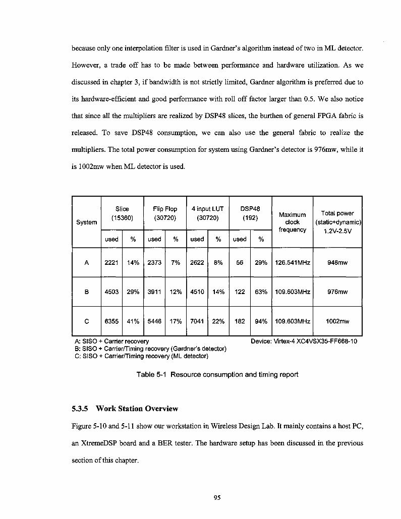
because only one interpolation filter is used in Gardner's algorithm instead of two in ML detector.
However, a trade off has to be made between performance and hardware utilization. As we
discussed in chapter 3, if bandwidth is not strictly limited, Gardner algorithm is preferred due to
its hardware-efficient and good performance with roll off factor larger than 0.5. We also notice
that since all the multipliers are realized by DSP48 slices, the burthen of general FPGA fabric is
released. To save DSP48 consumption, we can also use the general fabric to realize the
multipliers. The total power consumption for system using Gardner's detector is 976mw, while it
is 1002mw when ML detector is used.
System
A
B
C
Slice (15360)
used
2221
4503
6355
%
14%
29%
41%
Flip Flop (30720)
used
2373
3911
5446
%
7%
12%
17%
4 input LUT (30720)
used
2622
4510
7041
%
8%
14%
22%
DSP48 (192)
used
56
122
182
%
29%
63%
94%
Maximum clock
frequency
126.541MHz
109.603MHz
109.603MHz
Total power (static+dynamic)
1.2V-2.5V
948mw
976mw
1002mw
A: SISO + Carrier recovery Device: Virtex-4 XC4VSX35-FF668-10 B: SISO + Carrier/Timing recovery (Gardner's detector) C: SISO + Carrier/Timing recovery (ML detector)
Table 5-1 Resource consumption and timing report
5.3.5 Work Station Overview
Figure 5-10 and 5-11 show our workstation in Wireless Design Lab. It mainly contains a host PC,
an XtremeDSP board and a BER tester. The hardware setup has been discussed in the previous
section of this chapter.
95
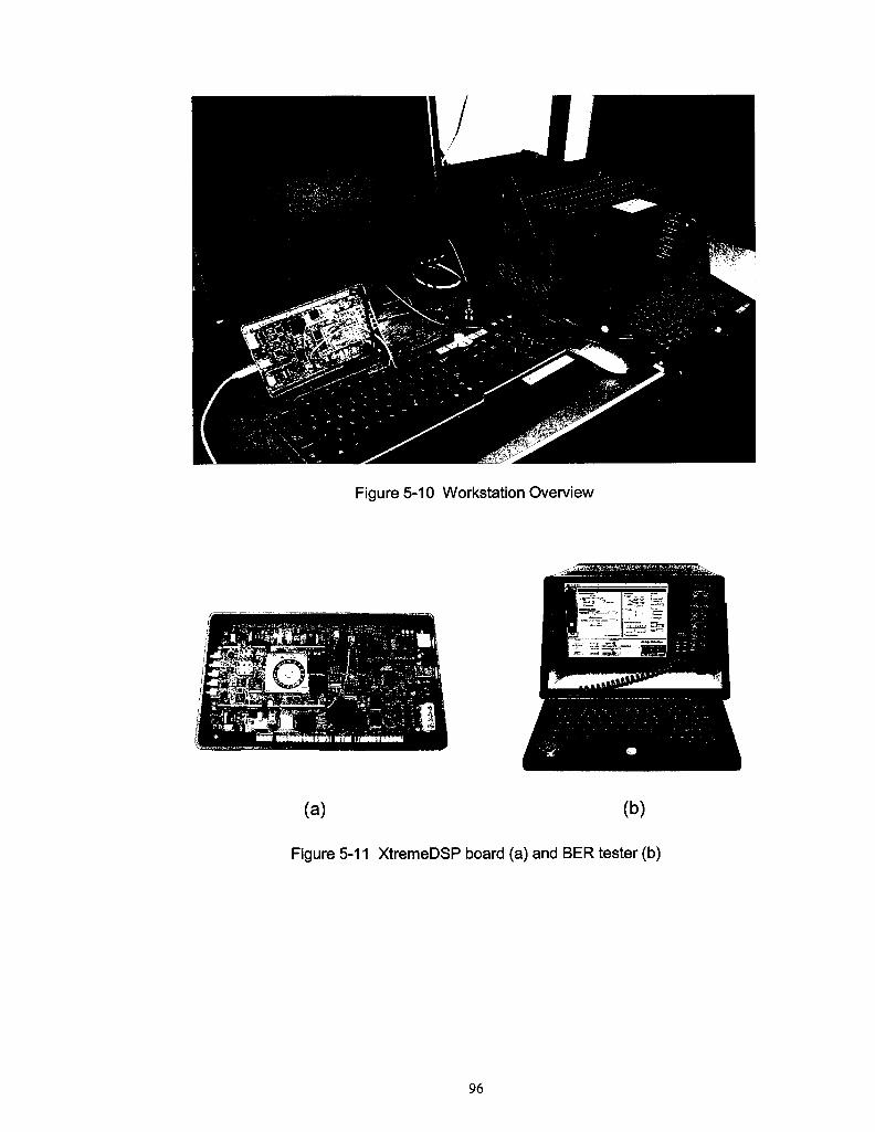
Figure 5-10 Workstation Overview
(a) (b)
Figure 5-11 XtremeDSP board (a) and BER tester (b)
96
Chapter 6
Conclusion and Future Work
6.1 Conclusion and Summary of the Thesis
In this thesis, an SDR based SISO system using QPSK modulation scheme is implemented on
FPGA. This system produces signal with an IF of 25 MHz and throughput of 12.5 Mbps. One
carrier recovery and two symbol timing recovery algorithms (Gardner and ML) are investigated
and implemented. A 2x1 MIMO system using Alamouti scheme and CORDIC based carrier
recovery is designed as well. The SDR based SISO system can be easily incorporated to the
MIMO design. Throughout this thesis, detailed design information of major components such as
baseband signal processing, synchronization, and digital up/down conversion is presented along
with both computer simulation results and real hardware performance. The comparisons of
different algorithms and component structures also provide information of choosing the suitable
algorithm or structure according to specific implementation considerations and system
requirement. The thesis is summarized as below.
In chapter 2, we explained the design and implementation of a SISO system with QPSK
modulation. The background and detailed design process are provided for each component. In
addition, the parallel polyphase structure for interpolation and decimation filter is proposed.
Compared with the MAC method, this structure is suitable for hardware with limited processing
speed but requiring high data rate.
97
The synchronization issues for SISO system are discussed in chapter 3. One carrier recovery
algorithm and two symbol timing recovery algorithms are investigated and designed. Simulation
results show that BER performance of proposed CR loop has 0.3 dB degradation compared with
ideal situation in an AWGN channel. On the other hand, in STR loop design, ML detector
performs better than Gardner's detector when the roll-off factor J3 is small. As ft increases, the
acquisition time of Gardner based design becomes shorter, and the BER performance approaches
ML based design.
In chapter 4, we discussed the design and implementation of a 2x1 MIMO system using
Alamouti scheme. The carrier recovery design using extended CORDIC algorithm is emphasized.
The simulation results show that the acquisition time of this CORDIC based design is 70 symbols,
and has less than 0.2 dB performance degradation in an AWGN channel in large SNR.
In chapter 5, the hardware test results of the SISO system design are presented. It shows that
the system with carrier and timing recovery implemented in the receiver has 1.2 dB
implementation losses. Furthermore, use of ML detector is hardware-cost, but provides better
performance than Gardner's detector when roll-off factor is small. However, if bandwidth is not
strictly limited, Gardner's detector is preferred due to its resources-efficiency and good
performance when roll-off factor is large.
6.2 Future Work
This thesis provides detailed information of FPGA based system design. It can be used as a base
for the ongoing and future projects conducted in Wireless Design Lab. The following is
recommended for future work:
• Most of the basic components in a practical system such as baseband signal processing,
synchronization, digital up and down conversion are successfully implemented in this thesis.
As a future work, a more complex and practical system design is to be designed and
98
implemented. The tasks include channel coding, space time coding, equalization, channel
estimation, power control and so forth.
• Due to the lack of a MIMO channel emulator, the MIMO system can not be tested at this
stage. However, this equipment will be available soon, and more complex MIMO system
design can be tested. As a future work, by using the powerful SignalMaster Quad platform
which consists of 4 high speed DSPs, 2 Virtex-4 FPGAs, totally 16 ADCs and DACs, 8
Gbps inter-FPGA channel and other impressive features, a MIMO system with up to 4
transmitters and 4 receivers can be implemented. Furthermore, with the help of the dual band
RF transceiver, the test of MIMO system in the real physical channel is also possible and
desired.
• FPGA is becoming a preferred choice for digital system implementation. The latest Virtex-6
devices use up to 759K logic cells with 6-LUT (64-bit ROM) technology, and supports up to
2016 XtremeDSP Slices with 25-bit by 18-bit multipliers. Mixed-mode clock managers are
also provided [53]. Due to the state-of-art hardware and software resources available in the
lab, more advanced signal processing techniques and various wireless protocols could be
implemented and tested. The recent techniques attracting both academia and industry include
3GPP LTE (Long term evolution), Wimax and combination of MIMO and OFDM, and so
forth.
99
Bibliography
[1] L. Pucker, "Finding MMO: A Proposed Model for Incorporating Multiple Input, Multiple
Output Technology Into Software Defined Radios", Proceedings of the SDR Forum SDR '05
Technical Conference, Nov. 2005
[2] SDR Forum, www, sdrforum.org
[3] C. Dick, "Design and implementation of high-performance FPGA signal processing
datapaths for software-defined radios" VMEbus Systems, August 2001
[4] M. Cummings, S. Haruyama, "FPGA in the Software Radio," IEEE Communications
Magazine, vol. 37, no. 2, pp. 108-112, Feb. 1999
[5] C. Dick and F. Harris, "FPGA QAM Demodulator Design," 12th international Conference
on Field Programmable Logic and Applications, Montpellier, France, Sept., 2002.
[6] F. Cardells et al., "Design of a DVB-S receiver in FPGA", 2003 IEEE Workshop on Signal
Processing Systems (SiPS 2003), Seoul Korea, Aug. 2003.
[7] F. Cardells et al, "Efficient FPGA-based QPSK Demodulation Loops: Application to the
DVB standard", 12th international Conference on Field Programmable Logic and
Applications, Montpellier, France, Sept, 2002.
[8] H. Tarn et al, "Designing Efficient Wireless Digital Up and Down Converters Leveraging
CORE Generator and System Generator," Xilinx Application Note, XAPP1018, Xilinx. Inc.,
Oct. 2007
[9] S. Creaney and I. Kostarnov, "Designing Efficient Digital Up and Down Converters for
Narrowband Systems," Xilinx Application notes, XAPP1113, Xilinx Inc. Nov. 2008
100
[10] Rob Pelt, "Wideband Modem Design Using FPGAs," in Proceeding of the SDR 04
Technical Conference and Product Exposition, 2004.
[11] S. W. Cox, J. A. Seely, "Rapid FPGA Modem Design Techniques For SDRs Using Altera
DSP Builder," Global signal processing conference & expos for the industry, 2004
[12] P. Murphy, F. Lou, and J. Patrick Frantz, "A hardware testbed for the implementation and
evaluation of MIMO algorithms," in Proceedings of the 2003 Conference On Mobile and
Wireless Communications Networks, Oct. 2003.
[13] A. van Zelst and T.C.W. Schenk, "Implementation of a MIMO OFDM-based wireless LAN
system," IEEE Trans. Signal Processing, vol.52, no.2, pp.483-494, Feb. 2004.
[14] W. Xiang, P. Richardson, B. Walkenhorst, X. Wang, and T. Pratt, "A High-Speed Four-
Transmitter Four-Receiver MIMO OFDM Testbed: Experimental Results and Analyses,"
EURASIP Journal on Applied Signal Processing, vol. 2006, pp. 1-10, 2006.
[15] K. Bialkowski, P. Uthansakul, M. Bialkowski, and A. Postula, "Design of MIMO Testbed
with an FPGA Board for Fast Signal Processing," 2006 Auswireless Conference, 2006.
[16] S. Caban, C. Mehlfhrer, R. Langwieser, A. L. Scholtz, and M. Rupp, "Vienna MIMO
testbed," EURASIP Journal on Applied Signal Processing, vol. 2006, pp. 1451-1458, 2006.
[17] K. Bialkowski et al, "2x2 MIMO testbed for dual 2.4GHz/5GHz band," International
Conference on Electromagnetics in Advanced Applications ICEAA, Italy, 2007
[18] D. Bates et al, "A 4x4 FPGA-based wireless testbed for LTE applications," IEEE 19th
International Symposium on Personal, Indoor and Mobile Radio Communications (PIMRC
2008) Sept. 2008.
[19] Xilinx System Generator for DSP, v 9.2 User Guide, Xilinx Inc., 2007
[20] B. Sklar, Digital Communications: Fundamentals and Applications, Second Edition,
Prentice Hall, PTR, 2001
[21] T, S. Rappaport, Wireless Communications: Principles and Practice, Prentice Hall,
New Jersey, 1996.
101
[22] J.G. Proakis, Digital Communications, Fourth Edition, New York: McGraw Hill, 2001
[23] K. Gentile, "The Care and Feeding of Digital, Pulse-Shaping Filters," RF Design magazine,
pp. 50-61, April 2002.
[24] Fliege, N. J. Multirate Digital Signal Processing: Multirate Systems, Filter Banks,
Wavelets, West Sussex, England: John Wiley & Sons, 1994.
[25] DDS v5.0 data sheet, Xilinx Product Specification, ds246, April, 2005
[26] C. Dick, Multirate Signal Processing, Prentice Hall PTR, 2001
[27] H. Meyr, M. Moeneclaey, and S. A. Fechtel, Digital Communication Receivers:
Synchronization, Channel Estimation, and Signal Processing. New York: Wiley, 1998.
[28] U. Mengali and A. N. D'Andrea, Synchronization Techniques for Digital Receivers. New
York: Plenum Press, 1997.
[29] L. Litwin, "Matched Filtering and Timing Recovery in Digital Receivers," RF Design
magazine, pp. 32-48, Sept. 2001
[30] C. Dick, F. Harris, and M. Rice, "FPGA Implementation of Carrier Synchronization for
QAM Receivers," Journal of VLSI Signal Processing, Kluwer, vol. 36, issue 1, pp. 57-71,
Jan. 2004.
[31] F. M. Gardner, "A BPSK/QPSK timing-error detector for sampled receivers," IEEE Trans.
Comm., vol. COM-34, no. 5, pp. 423^29, May. 1986.
[32] F. M. Gardner, "Interpolation in Digital Modems - Part I: Fundamentals," IEEE Trans.
Comm., vol. COM-41, pp. 501-507, Mar. 1993.
[33] F. M. Gardner, L. Eurp, and R. A. Harris, "Interpolation in Digital Modems - Part II:
Implementation and Performance," IEEE Transaction on Communications, vol. COM-41,
pp. 998-1008, Jun. 1993.
[34] C. Dick, F. Harris, and M. Rice, "Synchronization in software radios - carrier and timing
recovery using FPGAs," in Proceedings of 2000 IEEE Symposium on Field-Programmable
Custom Computing Machines, pp. 195-204, April 2000.
102
[35] F. Harris and M. Rice, "Multirate digital filters for symbol timing synchronization in
software defined radios," IEEE Journal on Select Areas in Communications, vol.19, pp.
2346-2357, Dec. 2001.
[36] Hwang and J. Ballagh, "Building Custom FIR Filters Using System Generator," 12th
international Conference on Field Programmable Logic and Applications, Montpellier,
France, Sept, 2002.
[37] S. M. Alamouti, "A simple transmit diversity technique for wireless communications," IEEE
Journal on Select Areas in Communications, vol. 16, pp. 1451-1458, Oct. 1998.
[38] B. Vucetic and J. Yuan, Space-Time Coding, John Wiley, 2003.
[39] D. Gesbert, M. Shafi, D. Shiu, P. Smith," From theory to practice: An overview of space-
time coded MIMO wireless systems ", IEEE Journal on Selected Areas on Communications
(JSAC). special issue on MIMO systems, April 2003
[40] F. Harris, C. Dick, and M. Rice, "Digital Receivers and Transmitters Using Polyphase Filter
Banks for Wireless Communications," IEEE Transactions on Microwave Theory and
Techniques, vol 51, no. 4, pp. 1395 -1412, April 2003.
[41] C. W. Farrow. "A Continuously Variable Digital Delay Element," In Proc. IEEE
International Symposium on Circuits and Systems (ISCAS '88), pp. 2641-2645, June 1988.
[42] M. Henker and G. Fettweis, "Combined Filter for Sample Rate Conversion, Matched
Filtering, and Symbol Synchronization in Software Radio Terminals," Proceedings of the
European Wireless, pp. 61-66, Sept. 2000.
[43] J. Vails and et al., "The use of CORDIC in software defined radios: A tutorial," IEEE
Communications Magazine, vol. 44, no. 9, pp. 46-50, Oct. 2006.
[44] Y.H. Hu, "CORDIC-Based VLSI Architectures for Digital Signal Processing," IEEE Signal
Processing Magazine, pp. 16-35, July 1992.
103

[45] A. shoari, M. kamarei, and A. Radmand, "Implementation of Costas loop using CORDIC
algorithm for software radio applications," in Proceedings of IEEE Communications, Vol.
152, No. 1, pp. 113-118,2005.
[46] D. R. Stephens, Phase-Locked Loops for Wireless Communications - Digital, Analog and
Optical Implementations, second edition, Kluwer Academic Publishers, 2002.
[47] V. Tarokh, H. Jafarkhani, and A.R. Calderbank, "Space-time block codes from orthogonal
designs," IEEE Transactions on Information Theory, vol. 45, pp. 1456-1467, July 1999.
[48] Virtex-4 FPGAs User Guide, v2.6, Xilinx Inc., Dec. 2008
[49] XtremeDSP Development Kit-IV User Guide, Issue 2, Xilinx Inc., 2005.
[50] XtremeDSP for Virtex-4 FPGAs User Guide, Xilinx Inc., 2005.
[51] FB100A BER Test System User Manual, FastBit Tech, Aeroflex Test Solutions, 2004.
[52] Virtex-4 Family Overview, Xilinx Inc., 2004
[53] Virtex-6 Family Overview, Xilinx Inc., 2009
104